Page 1
Transparent and Flexible Radio
Frequency (RF) Structures
by
Taehee Jang
A dissertation submitted in partial fulfillment
of the requirements for the degree of
Doctor of Philosophy
(Electrical Engineering)
in the University of Michigan
2017
Doctoral Committee:
Professor L. Jay Guo, Chair
Assistant Professor Neil Dasgupta
Associate Professor Anthony Grbic
Professor Kamal Sarabandi
Page 2
© Taehee Jang 2017
All Rights Reserved
Page 3
ii
To my father Dong Won Jang and my mother Kyeong Ja Kim
To my wife Myunghye Yoo and my daughter Yuna Jang
For their love, support, and dedication
Page 4
iii
ACKNOWLEDGEMENTS
First and foremost, I would like to sincerely express my gratitude to my advisor
Professor L. Jay Guo. He has been providing invaluable guidance and full support during
the whole process of my research. I have been learned many things from him including
technical knowledge, research methodologies, and communication skills. I truly appreciate
his patience, wisdom, encouragement and understanding which help me to get through
many difficult times during my research. I could not have achieved any of the
accomplishments without his support.
I would like to extend my sincere gratitude to my other committee members, Prof.
Kamal Sarabandi, Prof. Anthony Grbic, and Prof. Neil Dasgupta for devoting their time to
review this thesis and advising me with valuable suggestions. I also grateful that Dr. Adib
Nashashibi spent time discussing with me about measurements.
I would like to thank my colleagues and friends at Guo group, Radiation Laboratory
and EECS for constructive and insightful discussions. Many thanks to former members,
Prof. Hui Joon Park, Prof. Moon Kyu Kwak, Prof. Hongseok Youn, Dr. Jing Zhou, Dr.
Young Jae Shin, Dr. Yi-Kuei, Dr. Alex Kaplan, Dr. Jae Yong Lee, Dr. Kyu-tae Lee, Dr.
Taehwa Lee, Dr. Ashin Panday, and Andrew Hollowell. I am thankful to current members,
Sangeon Lee, Cheng Zhang, Long Chen, Chengang Ji, Qiaochu Li, Xi Chen, Suneel
Joglekar, Qingyu Cui for sharing their experiences and time with me. I also appreciate Dr.
Kyusang Lee, Hyunsoo Kim, Seungku Lee, Kyungun Jung, Jihun Choi, and Hyeongseok
Kim for their great help.
Page 5
iv
Last, but most importantly, I would like to express my deep appreciation to my dear
wife, Myunghye Yoo, and my family, including my parents, younger brother, for their
constant encouragement, unconditional love, and unfailing support. Especially, my special
thanks go to my beloved wife, Myunghye Yoo, for support and dedication. I couldn’t have
done this without the support of my wife. Thank you to my great and adorable daughter
Yuna Jang. I am truly blessed to have you in my life.
Page 6
v
TABLE OF CONTENTS
DEDICATION . . . . . . . . . . . . . . . . . . . . . . . . . . . . . . . . . . . . . . . . ... . . . . . . . . . . . . . . . ii
ACKNOWLEDGEMENTS . . . . . . . . . . . . . . . . . . . . . . . . . . . . . . . . . . . . . . . . . . . . . . iii
LIST OF FIGURES . . . . . . . . . . . . . . . . . . . . . . . . . . . . . . . . . . . . . . . . . . . . .. . . . . . . viii
LIST OF TABLES . . . . . . . . . . . . . . . . . . . . . . . . . . . . . . . . . . . . . . . . . . . . . . . . . . . . .xiv
ABSTRACT . . . . . . . . . . . . . . . . . . . . . . . . . . . . . . . . . . . . . . . . . . . . . . . . . . . . . . . . . ...xv
CHAPTER
1. Introduction……………………………...…………………………………….1
1.1 Background and Motivation……...……...……………………….……1
1.2 Thesis Outline …………..…………………...……………………...…4
2. Transparent and Flexible Polarization-Independent Microwave Broadband
Absorber ................................................................................................................7
2.1 Introduction............................................................................................7
2.2 Principle of Double Resonance...............................................................9
2.3 The design of Broadband Absorber .………………………...……….11
2.4 Absorber Simulation ………….……………………………………...14
2.5 Bi-static Scattering from Absorber…………………………………...17
2.6 Realization of the Transparent and Flexible Structure………………..21
2.7 Multi-layered Ultra Broadband Absorber……………………...……..27
2.8 Conclusion…………………………………………………..……….29
3. Semi-Transparet and Stretchable Mechanically Reconfigurable
Electrically Small Antennas Based on Tortuous Metallic Micromesh……...30
3.1 Introduction……………………………………………………….….30
3.2 Mechanically Reconfigurable Antenna Design…………………..…..33
Page 7
vi
3.2.1 Zeroth-order Resoannt Antenna Theory Based on Composite Right-
handed/Left-handed (CRLH) Transmission Line (TL)…………………..34
3.2.2 CPW-Fed Inductor-Loaded Zeroth-Order Resonant Antenna……...37
3.2.3 Analysis of Symmetric and Asymmetric CPW-fed ZOW Antennas..41
3.3 The Orientation of Meander Line…………………………………….43
3.4 The Design of Tortuous Micromesh……………………………...…..47
3.5 Antenna Fabrication and Measurement……………………...…….…52
3.6 Conclusion……………….…………….………………………….....60
4. Ultra-Low Profile Flexible Triple-polarized Antenna Using Flexible Silver
Nanowires and Substrate with High Isolation……………….…………….....61
4.1 Introduction..........................................................................................61
4.2 The Configuration of the Low-profile Tri-polarization Antenna.........63
4.2.1 The Comparison between Monopole Antenna and ZOR Array
Antenna…………………………………………………………………..67
4.3 Flexible Metallic Via Based on AgNWs……………….……………..69
4.4 Simulation and Measurement Results………………………………...71
4.5 Conclusion…………………………………………………………...74
5. Dual-Band/Tri-Polarized Metamaterial Antenna Based on Half-Mode
Hexagonal (HMH) Substrate Integrated Waveguide (SIW) Using Flexible
Substrate and Vias for WBAN Communications …………………………....75
5.1 Introduction…………………………………………………………..75
5.2 Half-Mode Hexagonal Substrate Integrated Waveguide……………..77
5.3 The Configuration of the Dual-band/Tri-polarization antenna Based on
Half-mode Hexagonal SIW………………………………………...…….82
5.4 Simulation and Measurement Results………………………………...86
5.5 Conclusion…………………………………………………………...90
6. Conclusions and Future Work……………………………………..………………..91
6.1 Summary of Achievements………………………......………………91
Page 8
vii
6.2 Future Works………………………………………………………....92
Bibliography…………………………………………………………...............………..96
Page 9
viii
LIST OF FIGURES
Figure
1.1. Landscape of electronics…………………………………………………………..2
1.2. Flexible electronics (a) on paper (b) on textile (c) on PET…………………………3
1.3. Transparent electronics (a) skin-like pressure and strain sensors (b) slot antenna
using AgHT-4 (c) neural micro-electrode arrays……………………………….....4
2.1. (a) Unit cell of absorber structure (b) Equivalent circuit model……………..……9
2.2. (a) Equivalent circuit at low frequency (b) Equivalent circuit at high frequency…10
2.3. Schematic of broadband absorber (perspective view)…………………………..…11
2.4. The design of unit cell (a) top view (design parameters: w1=4mm, w2=1mm,
l1=4.2mm, l=10mm). (b) Calculated real and imaginary part of impedance……..12
2.5. Simulated and measured absorption according to the frequency………………….14
2.6. (a), (b) represent the electrical amplitude on the top view at 7.4GHz and 10.1GHz
and power flow at 7.4GHz and 10.1GHz, respectively. (c), (d) The color represent
the amplitude of the electric field and the arrows represent the direction of the
electric field on the central cross section of unit cell at 7.4GHz and 10.1GHz,
respectively. (e), (f) The color represent the amplitude of the power flow and the
arrows represent the direction of the power flow on the central cross section of unit
cell at 7.4GHz and 10.1GHz, respectively…………………………........………..16
2.7. (a) Schematic of electric field and poynting vector localized in the gap between the
two bow-tie structures at the low resonant frequency. (b) Schematic of electric field
Page 10
ix
and pointing vector localized around the edges of the bow-tie structure at high
resonant frequency……………………………………………………………….17
2.8. (a) Model construction for the bistatic scattering calculation. (b) Field Calculator for
post-processing in Ansys HFSS………………………………………….………18
2.9. (a) Reflection at normal incidence (b) Reflection with and without bistatic scattering
calculation……………………………………………………………….……….20
2.10. (a) Simulated absorption at the different width of bow-tie (w1) (the 90% absorption
bandwidth at w1=1mm : 50.4%, at w1=2mm : 61.6%, at w1=3mm : 68.2%, at
w1=4mm : 72%) (b) Simulated absorption at the different width of bow-tie (t) The
inset shows the equivalent circuit model of the proposed absorber according to the
frequency………………………….……………………………………………...22
2.11. (a) Fabricated metallic bow-tie array on top of a flexible and transparent PET layer
(Scale bar = 100um) (b) Optical transmittance…………………………………...23
2.12. (a) Measurement set-up (b) Time gating in vector network analyzer……………..25
2.13. Measured absorptions at different polarization angle Φ.(0, 30, and 45 deg)……..26
2.14. (a) Ansys HFSS simulation model of two unit cells. (b) Absorption according to
the different incident angles (0˚, 20˚, 50˚, 60˚, and 70˚)…………………..….…27
2.15. Configuration of the multi-layer absorber structure (a) Perspective view (b) Top
view………………………………………………………………………..……28
2.16. Simulated absorption. (Wm1=1.6m, Wm2=2.2mm, Wm3=2.8mm, lm1=5.1mm,
lm2=10.8mm, lm3=19.4mm, t1=2.4mm, t2=2.2mm, and t3=4mm)…………………29
3.1. The configuration of transparent and mechanically reconfigurable antenna..........33
3.2. (a) Equivalent circuit model of the CRLH unit cell (b) Dispersion curve of the CRLH
unit cell..................................................................................................................34
Page 11
x
3.3. (a) The unit cell of epsilon negative (ENG) meta-structured transmission line (MTL)
(b) Equivalent circuit model of ZOR antenna.........................................................37
3.4. Dispersion disagram of the unit cell.........................................................................38
3.5. Electric field (a) Vector distribution on the antenna (b) The magnitude of electric
field at zeroth-order mode………………………………………………………...40
3.6. The relationship between frequency and the number of unit cells…………………41
3.7. CPW-fed ZOR antennas using (a) one symmetric unit cell (b) two asymmetric unit
cell (c) two symmetric unit cells…………………………………………………..42
3.8. Return losses for (a) one symmetric unit cell (b) two asymmetric unit cell (c) two
symmetric unit cells………………………………………………………………42
3.9. (a) CPW-fed ZOR antenna with larger ground planes (b) Measured return loss for
the CPW-fed ZOR antenna with and without larger ground planes……………….43
3.10. Simulated and measured transmission spectra of individual colors (blue, green, and
red) at normal incidence………………………………………………………….44
3.11. The change of vertical-oriented and horizontal-oriented meander lines with the
different tensile strains……………………………………………………………45
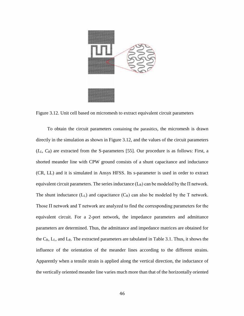
3.12. Unit cell based on micromesh to extract equivalent circuit parameters…………..46
3.13. Topology modification for transparent and stretchable micromesh.......................47
3.14. Mechanical simulation of micromesh....................................................................49
3.15. (a) Unit cell of micromesh using both tortuous wires in horizontal and longitudinal
direction (tortuous micromesh design 1) (b) Unit cell of micromesh using tortuous
wire in horizontal direction and straight wire in longitudinal direction one tortuous
(tortuous micromesh design 2)...............................................................................50
3.16. The schematic of the fabrication for micromesh………………………………..52
Page 12
xi
3.17. The fabricated transparent and stretchable antenna...............................................53
3.18. The resonant frequency according to the increase of strains (a) for antenna with
both tortuous lines (b) for antenna with only horizontal tortuous line (Solid line :
Simulated results, Dashed lines : Measured results)…………………………….54
3.19. The measured optical transmission of the stretchable antenna embedded in
PDMS…………………………………………………………………………..56
3.20. The radiation patterns (a) E-plane (xz-plane) (b) H-plane (xy-plane)……………57
3.21. A mechanically stretchable device …………………..…..………………...…….58
3.22. The radiation patterns in response to different tensile strains (0%, 20%, and
40%)…………………………………………………………………………….59
4.1. The configuration of Triple-polarized antenna system …………………………….62
4.2. (a) Perspective view of the antenna (shows port assignments and polarization
orientation) (b) top view of tri-polarized antenna. (Dimension [mm] of the antenna
are: w1 = 1.88, w2= 0.8, ws = 1, l1 = 3, lS = 45.72)………………………………….63
4.3. Simulated surface current distribution with different ports being excited: (a) at port1,
(b) at port 2……………………………………………………………………….64
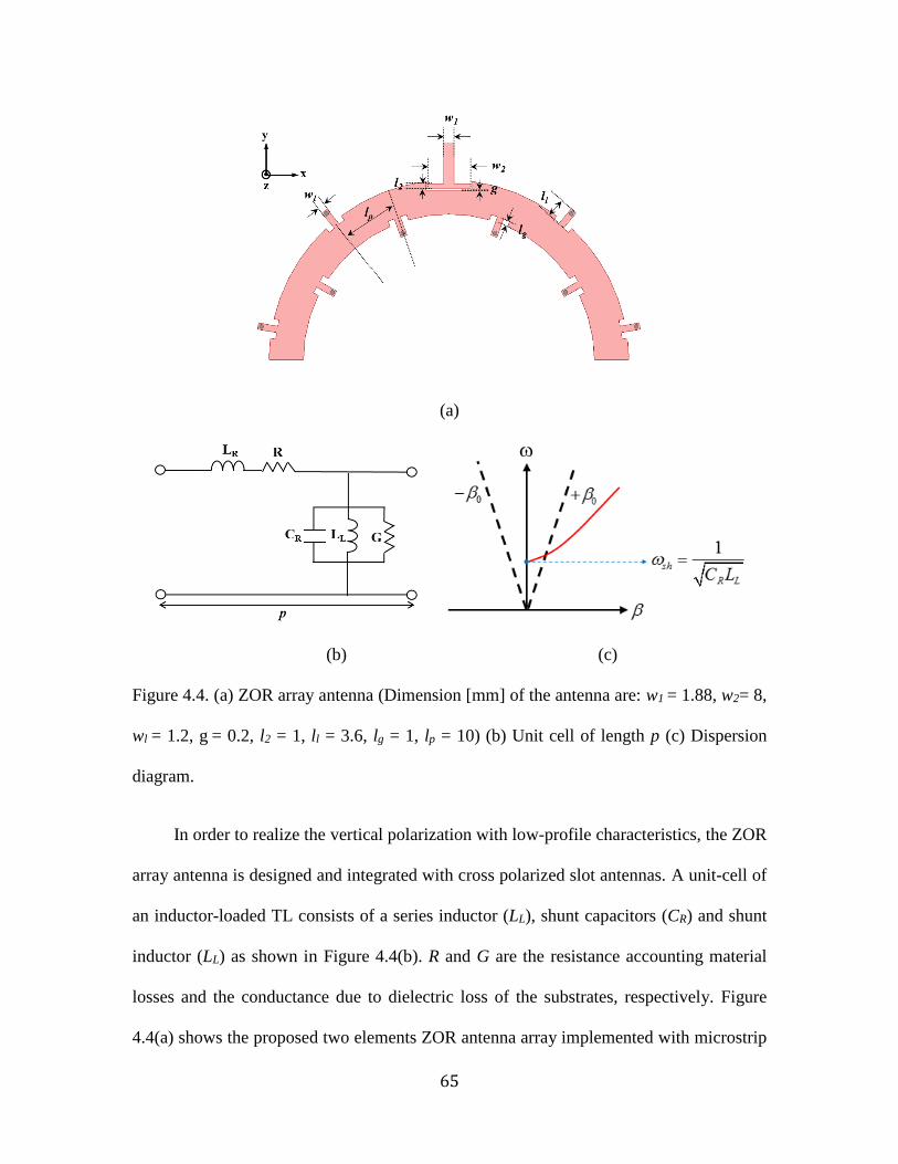
4.4. (a) ZOR array antenna (Dimension [mm] of the antenna are: w1 = 1.88, w2= 8, wl =
1.2, g = 0.2, l2 = 1, ll = 3.6, lg = 1, lp = 10) (b) Unit cell of length p (c) Dispersion
diagram.……………………………………………………………………….65
4.5. Simulated electric field vector distribution on the ZOR array antenna …………..67
4.6. (a) Configuration of monopole array antenna (Dimension: W=60mm, L=240mm,
H=41mm) (b) Return loss (c) Radiation patterns in terms of phase progression….67
4.7. (a) Configuration of ZOR array antenna (b) Radiation pattern……………………68
Page 13
xii
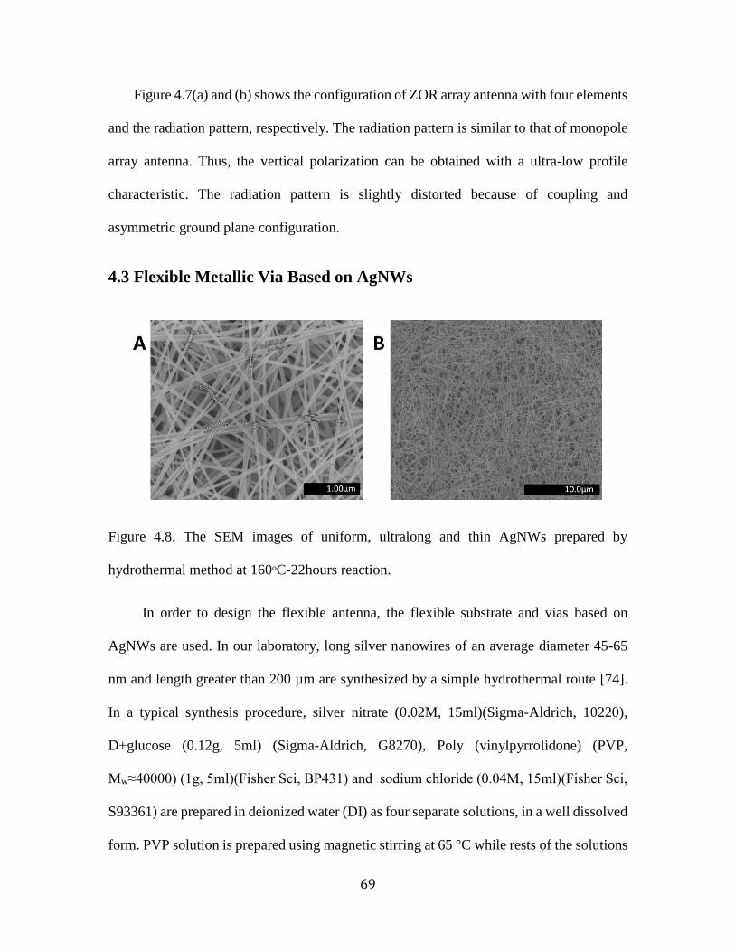
4.8. The SEM images of uniform, ultralong and thin AgNWs prepared by hydrothermal
method at 160ᵒC-22hours reaction. ……………………………………………....69
4.9. (a) Side view of AgNW via. (b) Fabricated AgNW via on the PCB substrate..........70
4.10. Fabricated the low-profile, flexible tri-polarized antenna using AgNW vias (a) Top
view (b) Bottom view………………………...........………………………………71
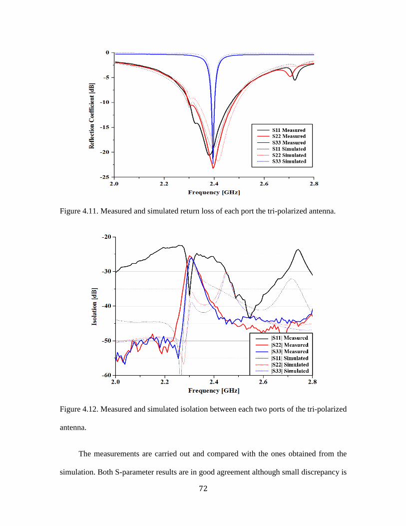
4.11. Measured and simulated return loss of each port the tri-polarized antenna.……..72
4.12. Measured and simulated isolation between each two ports of the tri-polarized
antenna…………………………………………………………………..……….72
4.13. Radiation patterns of the tri-polarized antenna (a) E-plane (+45 deg cut) at Port 1
(b) H-plane (-45 deg cut) at Port 1 (c) E-plane (-45 deg cut) at Port 2 (d)
H-plane (+45 deg cut) at Port 2 (e) E-plane (XZ-plane) at Port 3 (f) H-plane (XY-
plane) at Port 3……………………………………………………………………73
5.1. On-body communication and off-body communication in wireless body area
network (WBANs)………………..……………………………………………...76
5.2. Configuration of SIW structure ……………………………………………………78
5.3. Simulated magnitude of the total E-field distributions of (a) full-mode SIW, (b)
HMSIW, (c) triangular SIW, (d) hexagonal SIW (e) half-mode hexagonal SIW at
their dominant resonant frequencies (w=l=38mm).……………………………...…80
5.4. Simulated magnitude of the total E-field distributions of (a) full-mode SIW, (b)
HMSIW, (c) triangular SIW, (d) hexagonal SIW at their higher-order resonant
frequencies (w=l=38mm).……………………………………………………….…81
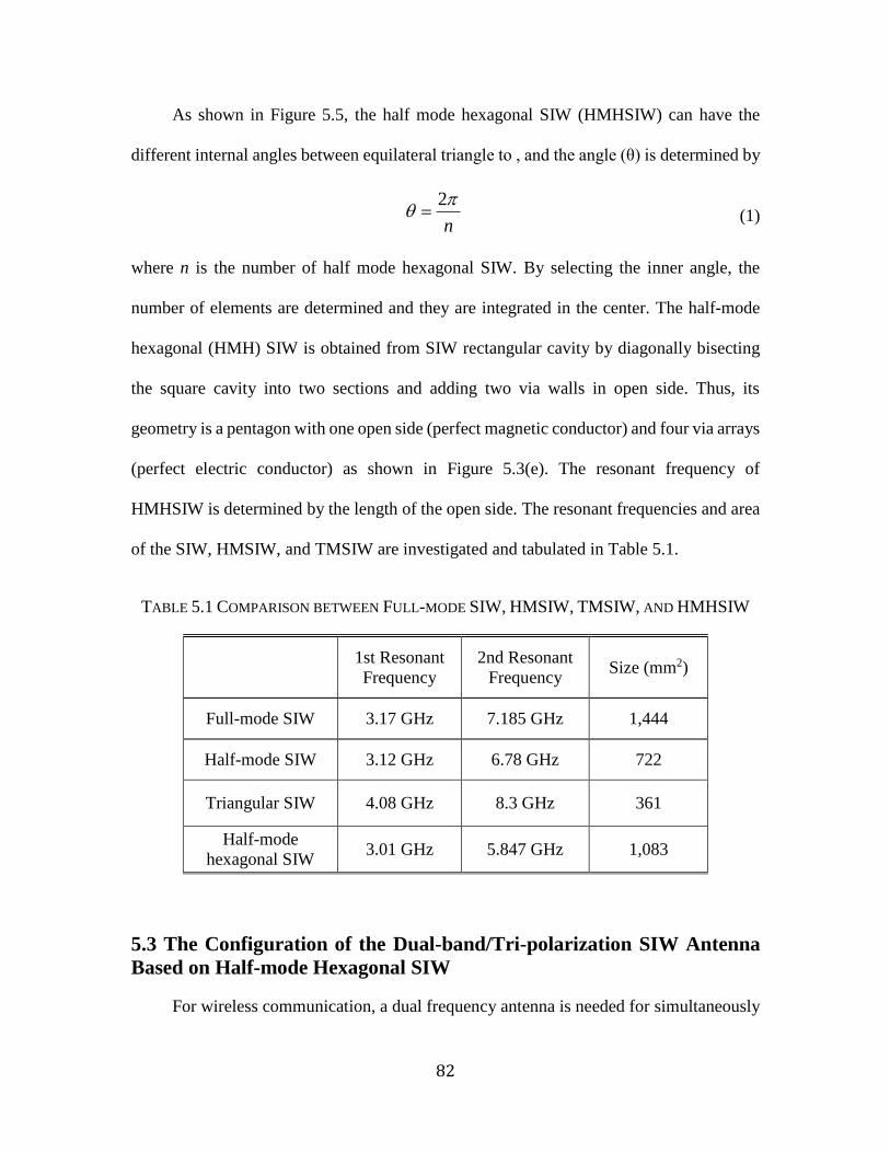
5.5. The configuration of the use of half-mode hexagonal SIW with the arbitrary internal
angle……………………………………………………………………………….81
Page 14
xiii
5.6. (a) Equivalent circuit model of a CRLH SIW unit cell. (b) General Dispersion
comparison between conventional half wavelength antenna and metamaterial
antenna.…………………………………………………………………………...83
5.7. (a) Perspective view of the dual-band tri-polarized antenna (a) Dual-band cross-
polarized CRLH HMHSIW antenna (b) Dual-band ZOR HMHSIW antenna.
(Dimension [mm] of the antenna are: wm1 = wz1 =1.87, wz2 =1.19, wz3 =0.3, wz4 =1.5,
wm2 = 1.5, lm2 = 6, ls = 6, ls1 = 3.5, gm1 = gm2 = gz1 = 0.2, rz1 =
0.7)……………………………………………………………..………………….85
5.8. The fabricated dual-band tri-polarized antenna based on half-mode hexagonal SIW
structure ………………………………………………………………………….87
5.9. Measured and simulated return loss of each port of the of the tri-polarized SIW
metamaterial antenna.…………………………………………………………….88
5.10. Measured and simulated isolation between each two ports of the of the tri-polarized
SIW metamaterial antenna.……………………………………………………….88
5.11. Measured and simulated radiation patterns of the proposed HMHSIW at both
frequencies (a) & (c) E-planes at n=-1st mode (b) & (d) E-planes at n=+1st mode
(e) 0th mode at lower frequency (f) 0th mode at higher frequency……………….89
6.1. (a) Pure Cyclic Olefin Copolymer (COC) grains (b) Heat-Pressure Imprinting
Process…………………………………………………………………….……..94
6.2. (a) COC-based SIW slot antenna (b) S-parameter………………………………..95
Page 15
xiv
LIST OF TABLES
Table
3.1. Inductance of meander line according to the orientations and tensile strains……..47
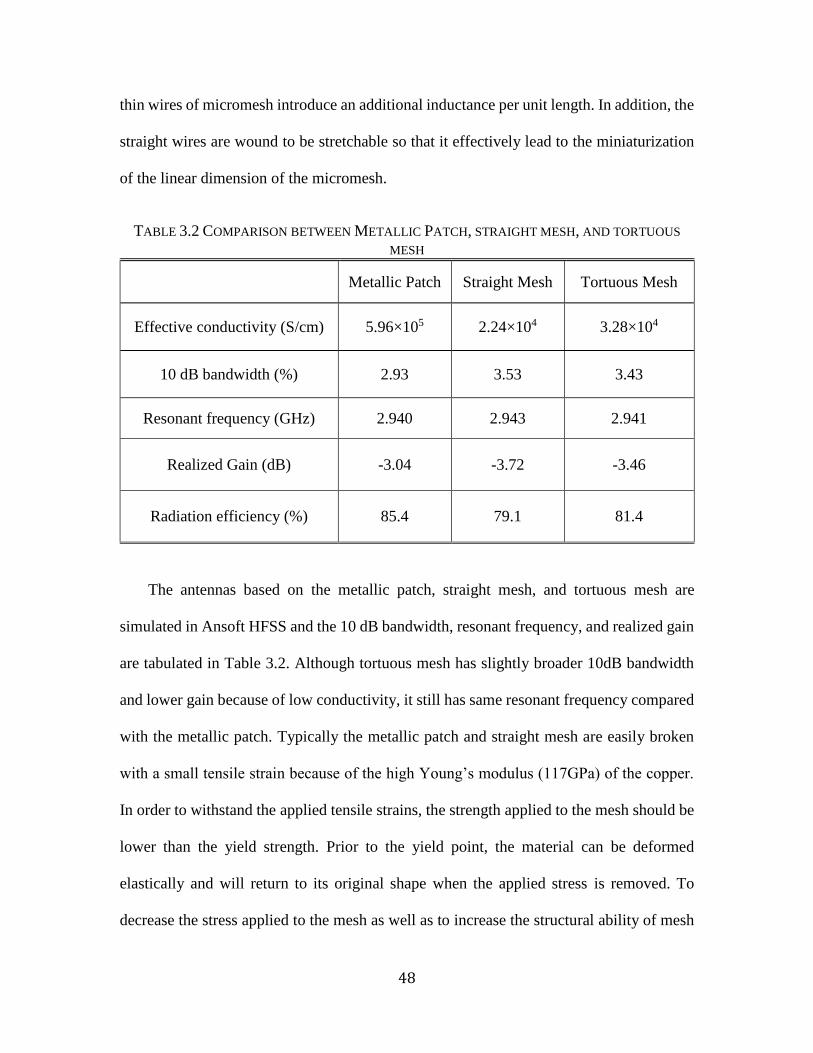
3.2. Comparison between metallic patch, straight mesh, and tortuous mesh…………...48
3.3. Relationship between optical transparency and electrical conductivity in terms of
the design of micromesh………………………………………………………….51
3.4. Bandwidth of proposed antenna……………………………………………….…56
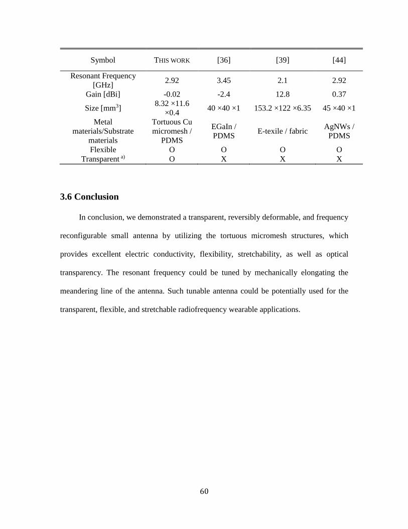
3.5. Antenna summary and comparison results for proposed and reference antennas….60
5.1. Comparison between full-mode SIW, HMSIW, TMSIW, and HMHSIW………...82
6.1. Properties of cyclic olefin copolymer………………………………………………94
Page 16
xv
ABSTRACT
Transparent and Flexible Radio Frequency (RF) Electronics
by
Taehee Jang
Chair: L. Jay Guo
With increasing demand for a wearable devices, medical devices, RFID, and small
devices, there is a growing interest in the field of transparent and flexible electronics. In
order to realize optically transparent and flexible microwave components, novel materials
can be used. The combination of new materials and radio frequency (RF) structures can
open interesting perspectives for the implementation of cost effective wireless
communication system and wearable device design. The transparent and flexible RF
structures can facilitate its application in the transparent and curved surfaces.
In this dissertation, we present several demonstrations, all based on optically
transparent and flexible materials and structures. We firstly demonstrate an optically
transparent, flexible, polarization-independent, and broadband microwave absorber. The
bow-tie shaped array which possesses double resonances is designed and measured. The
combined resonances lead to more than 90% total absorption covering a wide frequency
range from 5.8 to 12.2 GHz. Due to the use of thin metal and PDMS, the whole structure
is optically transparent and flexible. Secondly, we demonstrate a new method for
Page 17
xvi
fabricating transparent and stretchable radiofrequency small antennas by using stretchable
micromesh structures. Size reduction is achieved by using the zeroth-order resonant (ZOR)
property. The antennas consist of a series of tortuous micromesh structures, which provides
a high degree of freedom for stretching when encapsulated in elastomeric polymers and is
optically transparent. Accordingly, these antennas can be stretched up to 40% in size
without breaking. The resonant frequency of the antennas is linearly reconfigurable from
2.94 GHz to 2.46 GHz upon stretching. Next, we describe an ultra-low profile and flexible
triple-polarization antenna. It is realized by using ZOR array antenna with high port-to-
port isolation. This flexible antenna is fabricated with a flexible substrate and silver
nanowire vias to be used in various wearable applications. Lastly, we demonstrate a dual-
band tri-polarized antenna based on half-mode hexagonal (HMH) SIW structure. CRLH
HMHSIW antenna and ZOR HMHSIW antenna are designed to have dual-band operating
frequencies. This novel antenna can provide much improved wireless communication
efficiency for the WBAN system under various incident field angles and polarizations.
Page 18
1
Chapter 1
Introduction
1.1 Background and Motivation
With increasing demand for a wearable devices, medical devices, RFID, and small
devices, there is a growing interest in the field of transparent and flexible electronics. In
order to realize the optically transparenft and flexible microwave components, the use of
novel materials can open up new possibilities for implementation of microwave design and
applications.
Flexible electronics is a technology applied in electronic circuits by mounting
electronic devices on a flexible substrate. Flexible electronics have been integrated with a
variety of applications such as flexible circuits, flexible displays, flexible solar cells, skin-
like pressure sensors, and conformable radio frequency identification (RFID) tags. In
addition, the transparent electronics are a technology for realizing electronic circuits by
replacing with transparent structures or materials. Transparent electronics have been used
in a variety of applications such as transparent circuits, transparent display, transparent
solar cells, and transparent sensors. Given the benefits of these two kinds of technology, if
they could be combined in novel ways in such areas as radiofrequency electronics, it could
be possible to develop optically transparent and mechanically flexible radio frequency (RF)
electronics have opened a gate to next-generation technologies for the RF electronics that
Page 19
2
can be seen through and can be applied to a transparent or conformal object. Some work in
this area having done leading to advancements in RF electronics that have focused on
producing light weight, high performance RF electronics. Figure 1.1 shows the landscape
of electronics. The optical transparency and structural flexibility add another level of
complexity for designing radio frequency (RF) electronics because they are required to
have the similar performance of rigid and opaque electronics in spite of the use of
transparent and flexible materials.
Figure 1.1. Landscape of electronics
Many studies have already been conducted on the transparent and flexible
electronics. In the flexible electronics, flexible substrates such as paper, textiles, and PET
provides many properties that differ from those of polymide plastics used in conventional
flexible PCB technology [1-3]. Flexible electronics based on paper substrates with high
flexibility can be folded, easily disposed of, and trimmed with scissors. Paper substrates
also have other advantages such as low production costs and light weight. In the production
of paper substrate, the metallic patterns are printed onto the paper by evaporation, sputter
deposition, or spray deposition as shown in Figure 1.2(a) [4]. Electronic textiles (E-textiles)
Page 20
3
are fabrics that can communicate with other devices, transform signals, and conduct energy
which are impossible with traditional fabrics. To realize flexible electronics, the electronic
elements are integrated with E-textile. In [5], textile-based antenna to create a body area
network was used because it is bendable and comfortable enough to be easily inserted into
garments in Figure 1.2(b). Even when bent, this antenna could still have excellent
performance as well as be connected with radio module. Plastics have also been widely
used because they are very cheap and easily controllable materials. In Figure 1.2(c), the
mechanically flexible device was fabricated on the polyimide (PI) substrate. The ultrathin
molecular-monolayer-based devices can operate reliably when bent, twisted or deformed
into helical structures [6].
(a) (b) (c)
Figure 1.2. Flexible electronics (a) on paper (b) on textile (c) on PET
Many transparent materials such as glass, PET, and transparent film have been
exploited, all of which show promising characteristics. The optical transparency of
electronic devices can be obtained from the material properties or structural properties [7,
8]. In Figure 1.3(a), the pressure and strain sensors are realized by spray-depositing the
single-walled carbon nanotubes on PDMS substrate, so that it can be rendered stretchable
by applying strain along each axis [9]. The transparent antenna was fabricated on the glass
substrate by using the AgHT-4 film, with an operating frequency of 2.3GHz as shown in
Figure 1.3(b) [10]. Although AgHT-4 has lower gain compared to their copper
Page 21
4
counterparts, it allow the transmission of electric current while still retaining the optical
transparency. Figure 1.3(c) shows the transparent optogenetic brain implants that were
realized with gold pattern and four stacked single-atom-thick grapheme layers [11]. Thus,
it could remain reliable in various bending configurations, including the twisted and helical
structure.
(a) (b) (c)
Figure 1.3. Transparent electronics (a) skin-like pressure and strain sensors (b) slot antenna
using AgHT-4 (c) neural micro-electrode arrays
The combination of new materials and radio frequency (RF) electronics can open
interesting avenues for the implementation of cost effective wireless communication
system and wearable device design. The transparent and flexible radio RF electronics can
facilitate its application in the transparent and curved surfaces. Thus, my research focuses
on investigation of transparent and flexible RF devices, with an aim of new materials and
fabrication techniques.
1.2 Thesis outline
This thesis explores the optically transparent and structurally flexible radio frequency
electronics which can be applied to the transparent and curved surfaces. In the sections that
follow, the design objectives and principles of operation are presented.
Page 22
5
Chapter 2: Transparent and Flexible Polarization-Independent Microwave
Broadband Absorber
A polarization-independent broadband absorber with optical transparency and
structural flexibility is introduced and discussed in this chapter. These are the highly
desired properties for a wide variety of applications such as stealth ship and airplane. In
this chapter, we will also discuss how the absorption bandwidth can be improved. The
absorber is designed to have the double resonance, so that it can have broader bandwidth
by merging the double resonance.
Chapter 3: Semi-transparent and Stretchable Mechanically Reconfigurable
Electrically Small Antennas Based on Tortuous Metallic Micromesh
Chapter 3 describes the optically transparent and mechanically reconfigurable small
antenna based on the use of micromesh. Due to the transparency and flexibility, it can be
smoothly integrated with interiors and exteriors of electronic devices, such as cell phones,
laptops, and tablets. This mechanical tenability enables the broadband operation of the
small antenna to be efficiently utilized.
Chapter 4: Ultra-Low Profile Flexible Triple-Polarized Antenna Using Flexible Silver
Nanowires and Substrate with High Isolation
Chapter 4 presents a flexible triple-polarization antenna and discusses its great
potential applications such as WBAN network and MIMO. The omni-directional
horizontal polarization and conical vertical radiation patterns are obtained by using cross-
Page 23
6
polarized slot antennas and ZOR array antenna. A silver nanowires are used to realize the
flexible vias in the design.
Chapter 5: Dual-Band/Tri-Polarized Metamaterial Antenna Based on Polagon-Mode
(PM) Substrate Integrated Waveguide (SIW) Using Flexible Substrate and Vias for
WBAN communications
Chapter 5 describes a half-mode hexagonal substrate integrated waveguide (HMHSIW)
structure which can to reduce the size and efficiently integrate with other SIW structures
in a single elements. Since it operates at dual frequency bands, it can be used for
simultaneously transmitting and receiving these two bands. The dual-band tri-polarized
HMHSIW structure which four HMHSIW can be closely placed is designed, fabricated,
and analyzed.
Chapter 6 summarizes the main findings of each chapter, followed by future plans.
Page 24
7
Chapter 2
Transparent and Flexible Polarization-Independent
Microwave Broadband Absorber
2.1 Introduction
Broadband absorbers can reduce the reflection and scattering of electromagnetic (EM)
waves from the structures over a wide frequency range. Because of these characteristic,
they can be exploited to enhance the efficiency of photovoltaic devices [12, 13] and thermal
detectors [14], and can also render objects undetectable by EM waves [15]. Absorbers can
be designed by using classical electromagnetic wave theory or by engineered metamaterials.
Metamaterial absorbers have been designed by manipulating the effective permittivity ε(ω)
and permeability μ(ω) to match the impedance to free space [16-20]. Due to the lossy
components of permittivity and permeability, the structure is then able to the transmitted
power. Although metamaterial based absorbers offer the potential advantages of perfect
absorption and thin thickness, their use in practical applications is limited due to their very
narrow bandwidths. In order to improve the bandwidth, multi-band absorbers have been
introduced that utilize multiple layered structures [21, 22]. However, significant challenges
rise because these multilayered structures are thick and require a complicated fabrication
process. Another approach is classical electromagnetic absorbers, which can be realized by
Page 25
8
placing one or more additional resistive sheets in the structure to generate losses to the
incident field. One of the classic electromagnetic absorbers is Salisbury screen, which have
a resistive sheet placed at over a ground plane [23]. This absorber also has some
drawbacks similar to other structures such as narrow bandwidth and relatively large
thickness. Another classical absorber is the Jaumann absorber, which utilizes a multi-layer
structure to increase the bandwidth [24, 25]. However, to obtain the broad bandwidth, the
structure becomes very thick and bulky. A further weakness is that the absorbers
constructed from the conventional materials are typically rigid and optically opaque. If the
absorber can be made optically transparent and structurally flexible, it can provide high
design freedom for practical applications [26, 27]. For example, optically transparent and
flexible absorber can be applied to applications such as window glass and curved surfaces.
In this chapter, we propose and demonstrate an optically transparent, flexible,
polarization-independent, and broadband microwave absorber. The absorber is based on
two principles: 1) it utilizes resonant structure to provide the impedance match to the air,
such that EM energy can be coupled into the structure with little reflection; 2) the resonator
is made of Al wire grid to induce ohmic loss and effectively dissipates the coupled EM
energy to heat. We found that a bow-tie shaped resonator provides easy tunability of the
resonance bandwidth. The new structure is designed to possess two resonances resulting
from the symmetric bow-tie structures as well as the coupling between the neighboring
bow-tie structures. Therefore, the bow-tie array collectively provides a broadband
response. The symmetric bow-tie structure also provides a polarization-independent
property. The proposed structure is realized using an Al wire grid, transparent and flexible
Polyethylene terephtalate (PET) film, and Polydimethylsiloxane (PDMS) layers. The
4/
Page 26
9
overall structure is transparent and flexible, facilitating its application in curved surfaces.
The fabricated absorber structure produces the absorption above 90% in the frequency
range of 5.8-12.2GHz, and the bandwidth is 71.1% of the center frequency.
2.2 Principle of Double Resonance
(a) (b)
Figure 2.1. (a) Unit cell of absorber structure (b) Equivalent circuit model
Figure 2.1(a) shows the structure for achieving broadband absorption. Based on the
equivalent circuit as shown in Figure 2.1(b), the total impedance of the structure is
composed of the impedances of metallic resonator and dielectric layer with the ground
plane. The metallic resonator can be regarded as the series resonant circuit, so that its
impedance (Zs) is given by
1sZ R j L
j C
(2.1)
where C and L represent the capacitance and the inductance of resonant structure
respectively, and R is the resistivity from the ohmic loss of the metal.
Page 27
10
(a) (b)
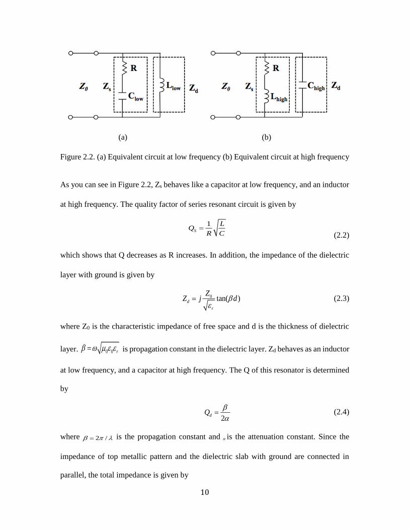
Figure 2.2. (a) Equivalent circuit at low frequency (b) Equivalent circuit at high frequency
As you can see in Figure 2.2, Zs behaves like a capacitor at low frequency, and an inductor
at high frequency. The quality factor of series resonant circuit is given by
1S
LQ
R C
(2.2)
which shows that Q decreases as R increases. In addition, the impedance of the dielectric
layer with ground is given by
0 tan( )d
r
ZZ j d
(2.3)
where Z0 is the characteristic impedance of free space and d is the thickness of dielectric
layer. 0 0 r is propagation constant in the dielectric layer. Zd behaves as an inductor
at low frequency, and a capacitor at high frequency. The Q of this resonator is determined
by
2dQ
(2.4)
where 2 / is the propagation constant and is the attenuation constant. Since the
impedance of top metallic pattern and the dielectric slab with ground are connected in
parallel, the total impedance is given by
Page 28
11
s d
total s d
s d
Z ZZ Z Z
Z Z
(2.5)
The resonance for the equivalent circuit occurs when Ztotal is matched to the free space
impedance. According to the change of frequency, Zs and Zd are changed and can have the
two kinds of equivalent circuit. Since the resonances occur when Ztotal matches the free
space impedance, the double resonance can occur as shown in Figure 2(c). Then, the two
resonances are merged to have a broad bandwidth. The total Q-factor is determined by the
parallel combination of Qs and Qd. High Q factor naturally leads to narrow band operation.
To achieve broadband absorption, we want to lower the total Q factor by increasing the
resistance R in the equivalent circuit model, and the increased resistance also has the
additional benefit of dissipating the energy, therefore result in minimized reflection. This
can be accomplished by using a very thin metal film to construct the resonant structure.
2.3 The Design of Broadband Absorber
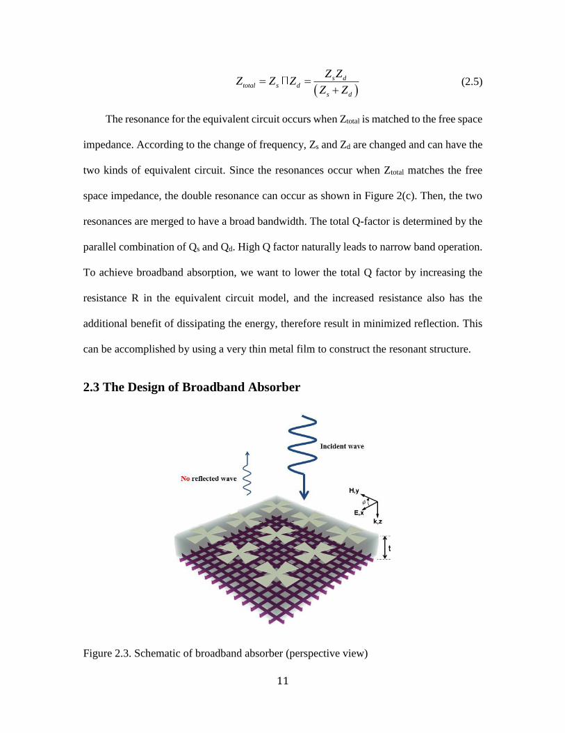
Figure 2.3. Schematic of broadband absorber (perspective view)
Page 29
12
In order to achieve perfect absorption, the impedance of the absorber is matched to
the air and then the transmitted waves are dissipated due to the loss components of the
structure. The previously reported experiment of concealing an object by a carbon nanotube
(CNT) coating across the entire visible band follows the same principle [18], where the
aligned CNTs with low fill ratio provided the index/impedance match to air; and also
absorb the light energy coupled into the CNT layer. However, if we attempted to extend
the approach to the microwave range, the required CNT thickness would be impractically
thick. To avoid this problem, we used an array of resonant structure to achieve the
impedance matching function.
(a) (b)
Figure 2.4. The design of unit cell (a) top view (design parameters: w1=4mm, w2=1mm,
l1=4.2mm, l=10mm). (b) Calculated real and imaginary part of impedance.
Figure 2.3 shows the structure used to achieve broadband absorption. The total
impedance of the structure is obtained from the combination of the impedances of the
metallic resonator and dielectric layer with the ground plane. The effective impedance of
the structure can be obtained from [19]
Page 30
13
2 2
11 21
2 2
11 21
( ) (1 )( )
( ) (1 )
eff
eff
eff
S SZ
S S
(2.2.1)
where ( )eff and ( )eff are the effective permittivity and permeability, respectively. The
real and imaginary part of the impedance are calculated from the simulated complex S-
parameters and plotted in Figure 2.4(b). The effective impedance of the structure has two
matched bands that result from the change of the electric and magnetic response
corresponding to the change of permittivity and permeability. This impedance matching
condition causes the reflected wave to be minimized.
The resonant structure having a high Q factor can be utilized in applications such as
narrow band filters and oscillators that require the high selectivity and low loss. In such
applications, broadband absorption can be achieved by reducing the Q factor of the
structure, which can be accomplished by increasing the resistance. This increased
resistance has the additional benefit of dissipating the energy, resulting in minimized
reflection over a broad frequency range. To increase the resistance, Al wire grid in a bow-
tie pattern is used to construct the resonant structure. For our design, we used bow-tie
shaped resonator, which has a symmetric configuration that is less sensitive to the
polarization of the incident wave. More importantly, we will show that the bow-tie shape
can offer a broader response range by exploiting not only its own resonance, but also the
coupling between the neighboring unit cells in a periodic array via the side of the bow-ties.
Regardless of the number of unit cells, the resonant frequency of the cascaded circuit is
determined by the resonant frequency originating from the two kinds of equivalent circuit.
By merging the two resonances, we achieved a broad bandwidth 71.1% of the center
frequency.
Page 31
14
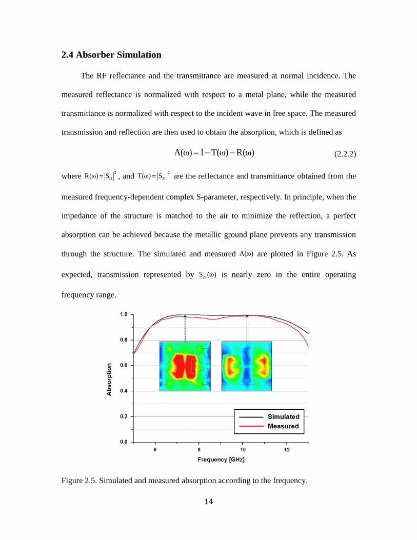
2.4 Absorber Simulation
The RF reflectance and the transmittance are measured at normal incidence. The
measured reflectance is normalized with respect to a metal plane, while the measured
transmittance is normalized with respect to the incident wave in free space. The measured
transmission and reflection are then used to obtain the absorption, which is defined as
(2.2.2)
where , and are the reflectance and transmittance obtained from the
measured frequency-dependent complex S-parameter, respectively. In principle, when the
impedance of the structure is matched to the air to minimize the reflection, a perfect
absorption can be achieved because the metallic ground plane prevents any transmission
through the structure. The simulated and measured are plotted in Figure 2.5. As
expected, transmission represented by is nearly zero in the entire operating
frequency range.
Figure 2.5. Simulated and measured absorption according to the frequency.
A( ) 1 T( ) R( )
2
11R( ) S 2
21T( ) S
A( )
21S ( )
Page 32
15
As can be seen in Figure 2.5, there are two absorption peaks; the low frequency is
mainly attributable to the coupling field between bow-tie structures and the high frequency
resonance is due to the fundamental resonant mode of bow-tie structure, as discussed
below. To understand the origin of these two absorption peaks, the electrical field
distribution and power flow are simulated and analyzed by using Ansys high frequency
structure simulator (HFSS) software. In the simulations, the top metallic wire grid bow-tie
resonators are modeled as an impedance sheet with a sheet resistance of 30 sq and the
dielectric constant and loss tangent of the dielectric spacer are 2.25 and 0.01, respectively.
A unit cell of the structure is simulated using periodic boundary conditions along the x and
y directions. The proposed absorber with w1 = 4mm has two resonances, one at 7.4GHz
and the other at 10.1GHz. Besides the simulation, as can be seen in Figure 2.4(b), we
calculated real and imaginary parts of impedance. The real part of impedance is almost
unity and the imaginary part of impedance is nearly zero between 7.4 GHz and 10.1GHz.
Therefore impedance matching with air was achieved, which minimizes the reflection from
the absorber. Figure 2.6(a) and (b) show the top view of the simulated electrical field
distribution of the absorber structure at the two absorption peak frequencies (f1=7.4GHz
and f2=10.1GHz), while Figure 2.6(c) and (d) show the simulated electrical field
distribution at the central cross section. The electric fields are strongly localized in the gap
between the two bow-tie structures at the low resonant frequency, and are localized around
the edges of the bow-tie structure at high resonant frequency. Figure 2.7(e) and (f) show
the power flow of the absorber at two absorption peak frequencies. Figure 2.7(a) and (b)
show the schematic of the electrical fields and power flows localized at low and high
resonant frequencies, respectively. The behavior is similar to that of magnetostatic
Page 33
16
interference [28] in metallic slit structures, where the polarized electric charge produces a
strong localized E-field, which guide the poynting energy flow, as shown in Figure 2.7(a)
and (b). At low resonant frequency, most incident power flows through the gap between
the bow-tie structures; while at high resonant frequency, the power flow is toward the
center of bow-tie resonator. In both cases, the energy flowing into the bow-tie eventually
dissipates in response to the high ohmic loss of the Al wire grid that is used to form the
bow-tie structure. These results verify that the two absorption peaks are a product of the
fundamental resonance of the bow-tie structure and the coupling between bow-tie
structures, respectively. The merging of the two resonances with overlap spectra ensures
the broadband performance of the proposed absorber.
(a) (b)
(c) (d)
(e) (f)
Page 34
17
Figure 2.6. (a), (b) represent the electrical amplitude on the top view at 7.4GHz and
10.1GHz and power flow at 7.4GHz and 10.1GHz, respectively. (c), (d) The color represent
the amplitude of the electric field and the arrows represent the direction of the electric field
on the central cross section of unit cell at 7.4GHz and 10.1GHz, respectively. (e), (f) The
color represent the amplitude of the power flow and the arrows represent the direction of
the power flow on the central cross section of unit cell at 7.4GHz and 10.1GHz,
respectively.
(a) (b)
Figure 2.7. (a) Schematic of electric field and poynting vector localized in the gap between
the two bow-tie structures at the low resonant frequency. (b) Schematic of electric field
and pointing vector localized around the edges of the bow-tie structure at high resonant
frequency.
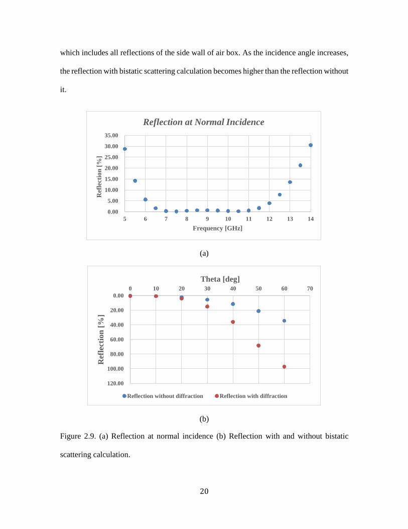
2.5 Bistatic Scattering from Absorber
Page 35
18
(a) (b)
Figure 2.8. (a) Model construction for the bistatic scattering calculation. (b) Field
Calculator for post-processing in Ansys HFSS.
A large filed is scattered in the specular direction; i.e., the angle of reflection is equal
to the angle of incidence. On the other hand, the reflected wave can be scattered to the other
directions because of the structural properties. Thus, the absorber scattering model is used
to examine the biscattering properties of our design in this section. Ansys HFSS is capable
of computing plane-wave scattering solutions. For a normal incidence, scattering solution
can be calculated using a waveguide simulation approach with port excitations. However,
since the off-normal incidence requires field post-processing for the data extraction from
plnae-wave excited solutions, the field post-processing for data extraction from plane-wave
excited solutions is used. The Ansys HFSS model for bistatic scattering measurement is
constructed as shown in Figure 2. 8(a). For incidence angle of arrival (0, θ), where θ=0-
60˚, Master/Slave phase relation is set to (180, θ) to correspond to the specular angle. The
Page 36
19
same variables are used in master/slave boundary setting. Thus, the incident wave varies
from normal to 60˚ incidence angles. The height of air on each side of the absorber is
considered as the necessary evaluation planes for the field calculator, and PML slabs are
added on the top and bottom of the air box. The linked boundary phase setting is changed
with the incidence angle.
Since minimum height to clear 60˚ angled plane is 2×tan(60˚)+λ/10, the height of the
air should be higher than 25 mm. The cut planes for the calculation are generated from the
geometry menu, and those are created normal to both the incident and the scattered ray
directions. The height of air on each side of the dielectric must consider the necessary
evaluation planes for post-processing. The cut plane for magnitude (or phase) integration
data cannot intersect the dielectric itself because of the very high reactive near fields. For
the post-processing, the field calculator is used to extract two quantities, incident
magnitude (Pinc) and reflected magnitude (Pref). Then these quantities are used to compute
reflection coefficient.
1( ) ( )( ) 2( )
1( )( ) ( )
2
ref refSref
incinc inc
S
E H dSP
PE H dS
(2.5.1)
Because the field calculator provides the RMS Poynting vector, the desired surface is
selected directly and integrated. The Poynting vector is calculated using only the E and H
field components of interest for the reflection. The calculated reflection at normal incidence
is plotted in Figure 2.9(a). The reflections with and without bistatic scattering calculation
are plotted in Figure 2.9(b), respectively. Blue dots shows the reflection magnitude when
the angle of reflection is equal to the angle of incidence. Red dots represent the reflection
Page 37
20
which includes all reflections of the side wall of air box. As the incidence angle increases,
the reflection with bistatic scattering calculation becomes higher than the reflection without
it.
(a)
(b)
Figure 2.9. (a) Reflection at normal incidence (b) Reflection with and without bistatic
scattering calculation.
0.00
5.00
10.00
15.00
20.00
25.00
30.00
35.00
5 6 7 8 9 10 11 12 13 14
Ref
lect
ion
[%
]
Frequency [GHz]
Reflection at Normal Incidence
0.00
20.00
40.00
60.00
80.00
100.00
120.00
0 10 20 30 40 50 60 70
Ref
lect
ion
[%
]
Theta [deg]
Reflection without diffraction Reflection with diffraction
Page 38
21
2.6. Realization of the Transparent and Flexible Structure
The proposed absorber is composed of top Al wire grid metallic patterned patches,
PET, PDMS, and metallic wire grid ground. Figure 2.3(a) shows the schematic of the
proposed absorber consisting of an array of Al wire grid metallic bow-tie resonators on a
PDMS dielectric layer backed by a metallic wire grid mesh ground plane. Figure 2.3(a)
shows the proposed absorber arranged in a periodic array, and figure 2.4(b) shows the unit
cell with the design parameters. A flexible and transparent PET and PDMS layer separate
the two metallic layers. Such flexible polymer layers with patterned bow-tie structures are
optically transparent, and can be applied to any metallic surface to provide the broadband
absorption property.
(a)
Page 39
22
(b)
Figure 2.10. (a) Simulated absorption at the different width of bow-tie (w1) (the 90%
absorption bandwidth at w1=1mm : 50.4%, at w1=2mm : 61.6%, at w1=3mm : 68.2%, at
w1=4mm : 72%) (b) Simulated absorption at the different width of bow-tie (t) The inset
shows the equivalent circuit model of the proposed absorber according to the frequency.
In designing the broadband absorber, the geometric parameters, including the
thickness of metallic patterns, are chosen to obtain the desired wave absorptions at two
resonance frequencies; and these parameters are further optimized so that the two
resonances are spectrally merged together to provide broadband characteristics. As an
example, Figure 2.10(a) shows that as base (w1) of the bow-tie increases, the absorption
band extends to lower frequency range. Here, the length of bow-tie and the spacing are
fixed to l =10mm and t = 5mm, respectively. In Figure 2.10(b), the thickness of the
substrate is changed from 3mm to 5mm. As the thickness decreases, the higher operating
spectrum is shifted into the higher band and the absorption became lower at the lower
Page 40
23
frequencies. To reduce the reflection from the absorber structure, good impedance
matching to air is required.
(a)
(b)
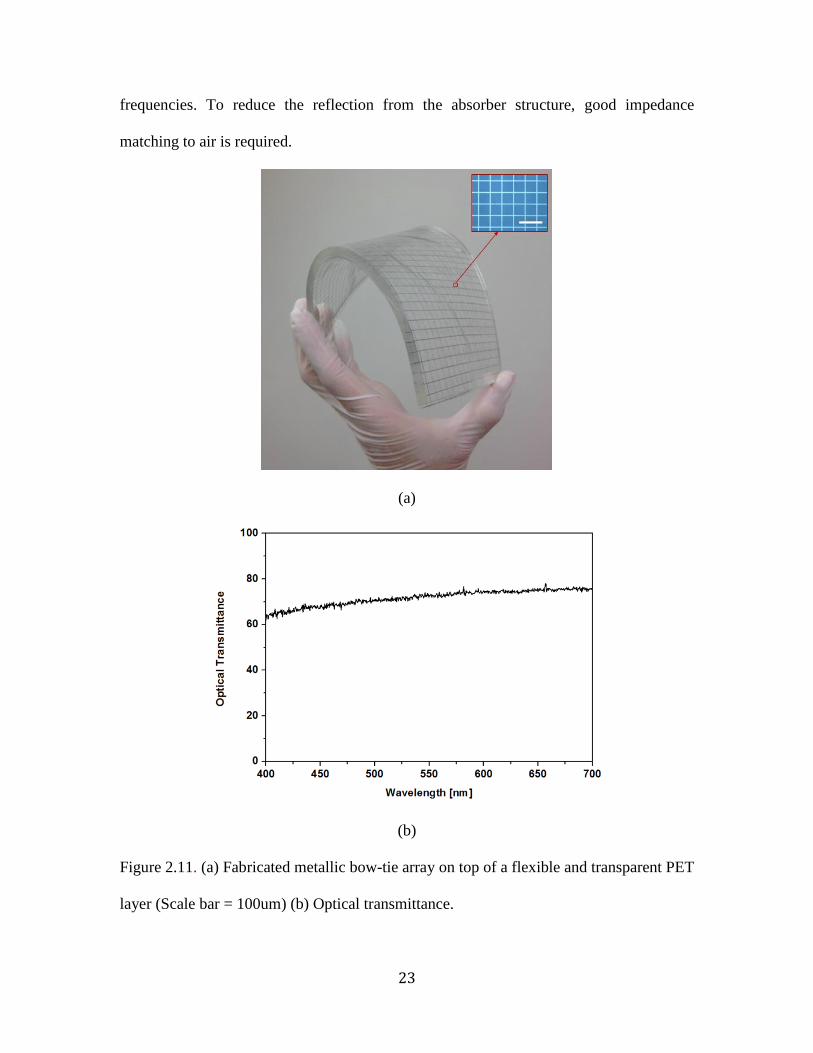
Figure 2.11. (a) Fabricated metallic bow-tie array on top of a flexible and transparent PET
layer (Scale bar = 100um) (b) Optical transmittance.
Page 41
24
This can be achieved by varying the spacing between bow-tie structure and dielectric
spacer layer thickness as well as using the optimized metal thickness. In order to obtain
greater than 90% absorption over the desired bands, the absorption magnitudes and
frequencies at the two resonances are optimized by adjusting the thicknesses of the
dielectric layer (PDMS) and the surface impedance of metallic wire grid bow-tie resonator
(Aluminum). For the bow-tie shaped resonator made of Al mesh with surface resistance of
30 sq , the optimized Al thickness is 62nm, while the PDMS layer with dielectric
constant 2.25 and thickness of 4.9mm is utilized for a spacer. The surface resistivity of the
deposited metal film was measured using a standard four-point probe configuration.
Furthermore, a transparent metal mesh ground plane that provides optical transparency
greater than 90% [29] is employed.
To fabricate the absorber structure having an area of 300mm 200mm, a 62nm-thick
aluminum was first deposited on a 50um-thick PET film by sputtering. The aluminum wire
grid mesh was then patterned in the shape of the bow-tie by optical lithography and etching.
Then the PET film with patterned Al structure is attached to a thicker and more flexible
PDMS layer. A picture of the fabricated bow-tie array on top of PET is shown in Figure
2.11(a). The inset in Figure 2.11(a) shows the zoomed view of bow-tie of Al wire grid
mesh. The fabricated structure is optically transparent, and when attached to a wire grid
metallic ground plane, forms a complete absorber structure.
Page 42
25
(a) (b)
Figure 2.12. (a) Measurement set-up (b) Time gating in vector network analyzer.
The absorber was measured by using a HP 8720B network analyzer that covers the
range of 0.13–20 GHz, and two broadband horn antennas in a microwave anechoic
chamber, as shown in Figure 2.12. As shown in Figure 2.12(b), the peak reflection is
obtained, and then the maximum peak is remained by using bandpass time gating in vector
network analyzer. The wire grid mesh ground plane can act as the metal plane at the
microwaves. The fabricated structure shows absorption greater than 90% is in the
frequency range of 5.8-12.2GHz and the bandwidth is 71.1% of center frequency. Figure
2.13 shows the measured absorptions for different polarizations of the incident wave. The
optical transmittance of total structure is more than 62% as shown in Figure 2.11(b). Due
to the symmetric pattern of bow-tie structure, the absorption is almost polarization-
Page 43
26
independent. The polarization angle ( ) is defined as the angle between the electric field
and x-axis.
Figure 2.13. Measured absorptions at different polarization angle Φ.(0, 30, and 45 deg).
Figure 2.13 shows the measured absorption according to the polarization. As the
increases, the absorption magnitudes and resonance frequencies of the absorber are nearly
unchanged for different polarizations (0, 30, 45 deg) of the normal incident wave,
demonstrating polarization-independence of the absorber structure. Figure 2.14(a) shows
the HFSS model of two unit cells based on bow-tie structures. Due to the Master/Slave
boundary pairs, the model represents infinitely periodic structure. Figure 2.14(b) shows the
simulated absorption according to the different incident angles (0˚, 20˚, 50˚, 60˚, and 70˚).
As the incident angle increases, the absorption peak at high frequency is shifted. The
absorption above 90% is achieved up to 54˚ of the incident angle as shown in Figure 2.14(b).
Page 44
27
(a) (b)
Figure 2.14. (a) Ansys HFSS simulation model of two unit cells. (b) Absorption according
to the different incident angles (0˚, 20˚, 50˚, 60˚, and 70˚).
2.7 Multi-layered Ultra Broadband Absorber
Finally we discuss methods to further increase the absorption bandwidth. Based on
the principle discussed above, even greater bandwidth can be obtained by merging multiple
resonances with overlap spectra. In order to achieve new resonances, bow-tie resonators
having different geometric parameters can be inserted in the dielectric spacer as
intermediate layers. In such a structure, each layer generates two resonant frequencies by
the similar principle. By adding patterned structures having the different lengths at
thickness of t1, t1+t2, and t1+t2+t3 respectively, different resonances can be obtained to
increase the bandwidth. For example, a 3 layer absorber is designed as shown in Figure
2.15(a). This structure avoids the alignment of the patterned bow-tie structures in each
layer as shown in Figure 2.15(b). As shown in Figure 2.15, the resonant fields are less
affected by the presence of the neighboring layers. In the simulation, the bow-tie resonators
Page 45
28
in the 1st, 2nd, and 3rd layers from the ground plane are modeled with the sheet resistances
of 20 sq , 20 sq , and 25 sq respectively.
(a) (b)
Figure 2.15. Configuration of the multi-layer absorber structure (a) Perspective view (b)
Top view.
Since the absorption peaks are located close to each other, the frequency range
needed to achieve absorption above 90% is 3.8-19.2GHz and, therefore the bandwidth of
the 3 layer absorber is enhanced to 133.9% of the center frequency, as shown in Figure
2.16. The metal mesh structure used in our structure not only provides optical transparency
but also increased resistance that is needed for the broadband application. To reduce
fabrication costs and time of our structure, large area of such flexible absorbers can be
fabricated in roll-to-roll platform using the recently developed photo roll lithography [29,
30], facilitating practical applications. With further development, we anticipate numerous
applications of such transparent and broadband absorbers in the future, e.g. zero-reflected
power over a wide bandwidth for better aircraft stealth performance.
Page 46
29
Figure 2.16. Simulated absorption. (Wm1=1.6m, Wm2=2.2mm, Wm3=2.8mm, lm1=5.1mm,
lm2=10.8mm, lm3=19.4mm, t1=2.4mm, t2=2.2mm, and t3=4mm).
2.8 Conclusion
In conclusion, the two absorption peaks are the result of energy flow and loss in
different positions of the absorber. Importantly, these peaks can be adjusted by changing
the width and length of the bow-tie structure respectively. Figure 2.6 shows that as the
width of bow-tie increases from 1mm to 4mm, the absorption peak at low frequency is
shifted to the lower frequency range in response to the increased coupling between the
neighboring bow-tie structures. Thus, the bandwidth needed to achieve more than 90%
absorption can be extended by increasing the w1. The spectral overlap of the two selected
absorption bands broadens the absorption bandwidth. In addition, owing to simple
periodically symmetric patterned structures, the absorber is independent to the
polarizations of the incident wave.
Page 47
30
Chapter 3
Semi-Transparent and Flexible Mechanically Reconfigurable
Electrically Small Antennas Based on Tortuous Metallic
Micromesh
3.1 Introduction
Recently, wearable technologies that aim to monitor person’s wellness or assist
people with diseases have attracted considerable interest. For wearable applications, a
variety of sensors, antennas, electronic circuits, and storage systems have been developed.
Not only should the wearable devices be small and light, but they should also be able to
communicate with other electronic devices. However, the antennas and battery are heavy
and take up a large amount of space in the system. In order to produce more compact and
lighter system, antenna integrated with a rectifying circuit can be employed to harvest RF
energy eliminating the need for the battery. Thus, a radio frequency antenna plays a
significant role in the wearable system.
The antennas for wearable applications should be able to be stretched, folded, and twisted.
A lot of flexible antennas, which are fabricated on a flexible copper-clad laminate, have
been researched [31, 32]. One challenge with using a flexible substrate is that the
Page 48
31
mechanical stability of the metal pattern and rigidity of the substrate are not sufficient for
wearable gadgets. To address this issue, stretchable antennas have been developed that use
a liquid metal such as mercury and eutectic gallium indium alloy (EGaIn) [33-37].
Although liquid metal antennas are mechanically tunable and have high degrees of
stretchability, the use of the liquid metal presents a challenge with regard to integration
with other system components (e.g. rectifying circuit and RF amplifier). A further
challenge is that the antenna may fail to operate properly due to the leakage of the liquid
metal if the sealing layer for the liquid metal is even slightly torn or has small holes.
Alternative to using liquid metal antennas is the textile-based antenna using metal-coated
polymer fibers (e-fibers) [38, 39]. To create such antenna, the conductive textile surface
was embroidered to form the antenna. However, because the e-fiber used in these antennas
is not stretchable, they are difficult to use for frequency-tunable applications. A further
drawback is that the efficiency of this antenna tends to be lower because of electrical
contact loss between the e-fibers and the high roughness of the textile.
In order to realize reconfigurable antenna, various mechanisms such as a switch and
varactor diode have been employed. Many reconfigurable antennas with electrical switches
(e.g. RF MEMs switch, pin diode, MEMs capacitor, and varactor diode) have been
developed by interconnecting the adjacent segments of the antenna elements [40]. For RF-
MEMs switch and pin diode, the reconfigurability is limited due to the discrete nature of
the switch [41-43]. In addition, since varactor diodes and MEMs capacitor provide variable
capacitance according to the voltage bias, continuous ranges of frequency reconfigurability
of the antenna are obtained [44, 45]. However, in order to operate the switches, a large RF
bias network is needed and the switches suffer from nonlinear effect and parasitic
Page 49
32
parameters. On the other hand, mechanical tunability could be exploited because it is
linearly tunable over a wide range of frequency band and does not require a bias network
[46-48]. Furthermore, optical transparency is desirable to meet the space requirement of
the wearable devices for practical applications (e.g. transparent smartphone and contact
lens display) [49]. Thus, the transparent antenna is intended for the wearable electronics or
implantable medical devices where it can be easily camouflaged. In order to provide the
optical transparency and electrical conductivity, graphene, nano-particle based electrodes
and ITO films have been studied for decades. However, studies have shown that due to the
low conductivity, relatively thick layers are needed in order to operate efficiently in the
desired radio frequency range. In addition, ITO film is rigid and brittle and therefore not
suitable for wearable applications.
This chapter describes a new method for fabricating transparent and stretchable
radiofrequency small antennas by using stretchable micromesh structures. These antennas
are smaller and lighter than the conventional antennas. Size reduction is achieved by using
the zeroth-order resonant (ZOR) property [50]. The antennas consist of a series of tortuous
micromesh structures, which provides a high degree of freedom for stretching when
encapsulated in elastomeric polymers and is optically transparent. Accordingly, the
structure can undergo mechanical deformation such as stretching, folding, or twisting
without breakage. These antennas can be stretched up to 40% in size without breaking and
easily return to their original shape after the force is removed. According to the increase in
the tensile strain, the resonant frequency of the antennas is almost linearly reconfigurable
from 2.94 GHz to 2.46 GHz. In addition, they are optically transparent due to the large
openings in the mesh and the optical transmittance have increased under high strains.
Page 50
33
Therefore, the proposed antennas could be used for the applications such as reconfigurable
antennas, antennas for transparent and curved spaces, and wearable sensors.
3.2 Mechanically Reconfigurable Antenna Design
Figure 3.1. The configuration of transparent and mechanically reconfigurable antenna.
Figure 3.1 shows a transparent and stretchable compact zeroth-order resonant (ZOR)
coplanar waveguide (CPW)-fed antenna. The antenna consists of the metallic patch,
shorted meander line, interdigital slot, and CPW ground. In order to be stretchable and
optically transparent, we replace the uniform metallic patches in the traditional antenna
configuration with a tortuous wire micromesh design. It can be replaced without loss of
Page 51
34
performance since the period of the mesh are roughly smaller than 0 /1100 [51], where
0
is free space wavelength.
3.2.1 Zeroth-order Resonant Antenna Theory Based on Composite Right-
handed/Left-handed(CRLH) Transmission Line(TL)
(a) (b)
Figure 3.2. (a) Equivalent circuit model of the CRLH unit cell (b) Dispersion curve of the
CRLH unit cell
A general CRLH TL is composed of series capacitance (CL) and inductance (LR) as
well as a shunt capacitance (CR) and inductance (LL), as shown in Figure 3.2. It is designed
in a periodic configuration by cascading N unit cells. The immittances of a lossy CRLH
TL are given by
1'series R
L
Z R j LC
(3.1)
1'shunt R
L
Y G j CL
(3.2)
Page 52
35
where R and G are the series resistance and shunt conductance of the lossy CRLH TL,
respectively. The series and shunt resonant frequencies are given by
1/se
R L
rad sL C
(3.3)
1/sh
L R
rad sL C
(3.4)
Thus, the complex propagation constant (γ) and characteristic impedance (ZC) are
' 'series shuntj Z Y (3.5)
2
2
' ( / ) 1
' ( / ) 1
series seL
C
shunt L sh
Z LZ
Y C
(3.6)
Because the CRLH TLs have periodic boundary conditions, the Bloch-Floquet
theorem can be applied and its dispersion relation is determined by
2
2
( ) 1( ) R L L R
R R
L LL L
L C L CsL C
Z L CL C
(3.7)
where s(ω) and ΔZ are a sign function and the differential length, respectively.
ωse and ωsh can be unequal in the dispersion diagram of the unbalanced LC-based
CRLH TL, as shown in Fig. 3.2(b). At these resonant frequencies, where β = 0, an infinite
wavelength can be supported. According to the theory of the open-ended resonator with
the CRLH TL, its resonance occurs when
( 0, 1,..., ( 1))n
n Nnl
(3.8)
Page 53
36
where l, n and N are the physical length of the resonator, mode number, and number of unit
cells, respectively. When n is zero, the wavelength becomes infinite and the resonant
frequency of the zeroth-order mode becomes independent of the size of the antenna, while
the shortest length of the open-ended resonator is one half of the wavelength. Thus, an
antenna with a more compact size can be realized.
As shown in Fig. 3.2(b), two resonant frequencies, ωse and ωsh, with β = 0 for the
unbalanced CRLH TL are observed with a matched load. Considering the open-ended TL,
where ZL = ∞, the input impedance (Zin) seen from one end of the resonator toward the
other end is given by
0 1cot( )open
in c cZ jZ jZ
' 1 1 1
' '' '
series
shunt shuntseries shunt
Zj
Y Yj Z Y
1
' ( )shuntY N z
(3.9)
where Y'shunt is the admittance of the CRLH unit cell.
Since, from Eq. (3.9), the input impedance of the open-ended resonator is equal to
1/N times 1/Y'shunt of the unit cell, the equivalent L, C, G values are equal to LL/N, NCR, and
1/NG, respectively. Regardless of N, the resonant frequency of the N cascaded open-ended
ZOR circuit is determined by the resonant frequency originating from the shunt LC tank
(Y'shunt). Thus, the open ended ZOR antenna's resonant frequency is given by Eq. (3.4),
resulting in depending only on the shunt parameters of the unit cell.
Considering that the open ended resonator is only dependent on Y'shunt of the unit cell,
the average electric energy stored in the shunt capacitor, CR, is given by
Page 54
37
21
4e RW V NC
(3.10)
and the average magnetic energy stored in the shunt inductor, LL, is
2 2
2
1 1
4 4
L
m L
L
L NW I V
N L
(3.11)
where IL is the current through the inductor.
Because resonance occurs when Wm is equal to We, the quality factor can be calculated
as follows:
( )
( / sec )
average energy storedQ
energy loss ond
2 1/ 1/
( / )
m
sh
loss sh L sh L
W NG G
P L N L
(1/ ) (1/ )sh R sh RNG NC G C
1 R
L
C
G L (3.12)
3.2.2 CPW-fed Inductor-Loaded Zeroth-Order Resonant Antenna
(a) (b)
Page 55
38
Figure 3.3. (a) The unit cell of epsilon negative (ENG) meta-structured transmission line
(MTL) (b) Equivalent circuit model of ZOR antenna
Figure 3.4. Dispersion disagram of the unit cell
Figure 3.3(b) depicts an infinitesimal circuit model for the lossless unit cell of ENG
MTL model which is represented as the combination of a per-unit length series inductance
(LR), and a shunt capacitance (CR), and a per-unit length shunt inductance (LL). The shunt
components of the unit cell are obtained from the shunt capacitance between the top patch
and CPW ground, and a shunt inductance of the shorted meander lines as shown in Figure
3.3(a). In addition, the LL and CR include additional inductance and capacitance formed by
the tortuous metal micromesh. The coupling capacitance (Cc) created by an interdigital
capacitance in the equivalent circuit model of ZOR antenna is introduced and responsible
for only impedance matching. Given that only shunt components (YENG) of the unit cell
determine the resonant frequency of the open-ended resonator, the average electric energy
and the average magnetic energy are stored in the shunt capacitor (CR) and the shunt
inductor (LL), respectively. From an infinitesimal circuit model for the lossless unit cell of
Page 56
39
epsilon negative (ENG) meta-structured transmission line (MTL) model, the effective
permeability and permittivity of the MTL materials are obtained as
2
1ENG
ENG R
L
YC
j L
(3.13)
ENG
ENG R
ZL
j
(3.14)
where Z and Y are the per-unit length impedance and admittance, respectively [50, 52, 53].
If the frequency band (ω) is smaller than 1/ L RL C , the ENG MTL has positive permeability
and negative permittivity so that it has single negative stopband. The ENG has the unique
characteristic of an infinite-wavelength wave at the boundary of passband and stopband.
Therefore, zeroth-order resonance occurs when the MTL has zero permittivity. Based on
the open-ended structure, the resonant frequency of the mechanically reconfigurable
antenna based on ENG MTL is determined by
1[1 ]
L R
sL C
(3.15)
where LL is the inductance of shorted meander line and CR is the capacitance between the
metallic patch and CPW ground respectively as shown in Figure 3.3(a). It indicates that the
ZOR frequency is determined only by the shunt inductance and capacitance and therefore
independent of the physical length of the resonator. Thus, a small antenna based on the
zeroth-order condition is implemented and the resonant frequency of the antenna can be
controlled with applied mechanical force. Figure 3.4 illustrates the dispersion diagram for
the proposed unit cell. It is based on the S-parameters obtained from the driven mode
simulation results. Since this antenna is realized by the inductor-loaded unit cells, the
Page 57
40
dispersion diagram only shows the phase delay characteristic. Therefore, the negatice
resonance is effectively eliminated while maintaining the zeroth-order resonance.
(a) (b)
Figure 3.5. Electric field (a) Vector distribution on the antenna (b) The magnitude of
electric field at zeroth-order mode
The structure based on the CPW-fed zeroth order resonant property had been verified.
As shown in Figure 3.5(a), the electric field distribution of the zeroth-order resonant
antenna is in-phase. At the zeroth-order resonant frequency, the resonant condition is
independent of the aperture dimension. Figure 3.6 shows the magnitude of electric field at
zeroth-order mode. Since the magnitude of the electric field in the interdigital slot is more
dominant than others, the interdigital slot makes the main contribution ot the antenna
radiation pattern. In general, both microstrip and CPW resonant antennas radiate from slots.
In Ref. [52], the microstrip ZOR antenna’s radiation mechanism is same as well. The
constant magnetic loop current source is generated by the constant E-field distribution in
four slots. Although the proposed CPW ZOR antenna is similarly radiating from slots, the
dominant magnetic current source is one slot which is located at the feeding line. The other
magnetic current sources from three slots are weaker because the signal and ground planes
are far away. Accordingly, this antenna looks like an ideal magnetic dipole rather than a
Page 58
41
magnetic loop. As a result, the E-plane and H-plane of the proposed antennas become yz-
plane and xz-plane by duality, respectively. Generally, the discontinuity in CPW structure
makes less radiation than the microstrip. The asymmetric antenna has more discontinuity
than symmetric antenna. Therefore, the efficiency of asymmetric antenna is lower because
of the coupled slot mode as well as the small electrical size.
Figure 3.6 clearly demonstrates that the resonant frequencies remain almost constant
as the aperture dimension is increased. In conventional resonant antenna, it is obvious that
the resonant frequency is decreased as its size is increased.
Figure 3.6. The relationship between frequency and the number of unit cells
3.2.3 Analysis of Symmetric and Asymmetric CPW-Fed ZOR Antennas
Since our proposed antenna has electrically finite ground plane and an unbalanced
structure, CPW-fed ZOR antennas that consist of asymmetric and symmetric structures as
shown in Figure 3.7 are studied for the effects of finite ground plane and unbalanced
structure in this Chapter. Figure 3.7(a) represents the one unit cell of symmetric antenna.
Figure 3.7(b) and 3.7(c) show the CPW-fed ZOR antenna using two asymmetric and
Page 59
42
symmetric unit cells, respectively. Since the resonant frequency are determined from the
shunt inductance and capacitance, three antennas have the different operating frequencies.
The measured return loss are plotted in Figure 3.8.
(a) (b) (c)
Figure 3.7. CPW-fed ZOR antennas using (a) one symmetric unit cell (b) two asymmetric
unit cell (c) two symmetric unit cells
Figure 3.8. Return losses for (a) one symmetric unit cell (b) two asymmetric unit cell (c)
two symmetric unit cells
The proposed design is validated using a large ground plane and balanced structures
as shown in Figure 3.9(a) [54]. First of all, a large ground plane is added on the CPW
ground of the proposed antenna and measured by a vector network analyzer. The resonant
Page 60
43
frequency of the antenna with a large ground plane are slightly different from those of the
same antenna on a finite ground plane. Figure 3.9(b) shows the measured reflection
coefficient for the CPW-fed ZOR antenna with and without larger ground planes. As the
ground size becomes larger, the effect from the cable is reduced.
(a)
(b)
Figure 3.9. (a) CPW-fed ZOR antenna with larger ground planes (b) Measured return loss
for the CPW-fed ZOR antenna with and without larger ground planes.
3.3 The Orientation of Meander Line
Page 61
44
In addition, to obtain the change the inductance (LL) by applying mechanical means,
the vertically oriented meander line is used than the horizontally oriented meander line in
our antenna as shown in Figure 3.3(a)
(a) (b)
Figure 3.10. Simulated and measured transmission spectra of individual colors (blue, green,
and red) at normal incidence.
Figure 3.10(a) and (b) show the meander-shape inductors positioned in a vertical and
a horizontal orientations, respectively. The meander line is connected between the metallic
patch and CPW ground as shown in Figure 3.3(a). It can be modeled as an equivalent
inductor because it is considered as shorted transmission line. In order to realize the
meander line, the tortuous meshed conductors are orthogonally placed. The vertically-
oriented meander line has longer conductors with length 1vl and width
1vw in the direction of
force and shorter conductors with length 2vl and width
2vw in the perpendicular direction of
force as shown in Figure 3.6(a). Appropriate self and mutual inductance values are
determined by the optimal arrangement of the size parameters. According to the applied
tensile strains, the parameters of the vertically-oriented meander line are changed. The 1vl
Page 62
45
and 2vw increases, and
2vl and 1vw decreases. The horizontally-oriented meander line
consists of shorter conductors with length 2hl and width
1hw in the direction of force and
longer conductors with length 1hl and width
2hw in the perpendicular direction of force as
shown in Figure 3.10(b).
When the tensile strain is applied in the vertical direction as shown in Figure 3.11,
the 2hl and
2hw of the horizontally-oriented meander line increases, but 1hl and
1hw decreases.
The inductances and capacitances are extracted from a circuit (Advanced Design System
2015) and full wave (Ansoft HFSS 15) simulator regarding the meander line shapes and
applied tensile strains.
Figure 3.11. The change of vertical-oriented and horizontal-oriented meander lines with
the different tensile strains.
Page 63
46
Figure 3.12. Unit cell based on micromesh to extract equivalent circuit parameters
To obtain the circuit parameters containing the parasitics, the micromesh is drawn
directly in the simulation as shown in Figure 3.12, and the values of the circuit parameters
(LL, CR) are extracted from the S-parameters [55]. Our procedure is as follows: First, a
shorted meander line with CPW ground consists of a shunt capacitance and inductance
(CR, LL) and it is simulated in Ansys HFSS. Its s-parameter is used in order to extract
equivalent circuit parameters. The series inductance (LR) can be modeled by the Π network.
The shunt inductance (LL) and capacitance (CR) can also be modeled by the Τ network.
Those Π network and Τ network are analyzed to find the corresponding parameters for the
equivalent circuit. For a 2-port network, the impedance parameters and admittance
parameters are determined. Thus, the admittance and impedance matrices are obtained for
the CR, LL, and LR. The extracted parameters are tabulated in Table 3.1. Thus, it shows the
influence of the orientation of the meander lines according to the different strains.
Apparently when a tensile strain is applied along the vertical direction, the inductance of
the vertically oriented meander line varies much more than that of the horizontally oriented
Page 64
47
meander line. Thus, the vertically oriented meander line is preferred to obtain widely
mechanically tunable resonances.
TABLE 3.1 INDUCTANCE OF MEANDER LINE ACCORDING TO THE ORIENTATIONS AND
TENSILE STRAINS
TENSILE STRAIN (%) 0% 20% 40%
MTL with
vertically oriented
meander line
Inductance (nH) 6.323 7.519 8.271
Capacitance (pF) 0.451 0.434 0.493
Resonant frequency (GHz) 2.98 2.78 2.49
MTL with
horizontally
oriented meander
line
Inductance (nH) 6.198 6.287 6.497
Capacitance (pF) 0.452 0.463 0.456
Resonant frequency (GHz) 3.01 2.95 2.92
3.4 The Design of Tortuous Micromesh
Figure 3.13. Topology modification for transparent and stretchable micromesh.
The metallic patch of the antenna in Figure 3.13 can be replaced with micromesh to
be optically transparent as well as to have good electric conductivity. The electric current
distribution on an ordinary metallic patch at the zeroth-order mode is not changed, but the
Page 65
48
thin wires of micromesh introduce an additional inductance per unit length. In addition, the
straight wires are wound to be stretchable so that it effectively lead to the miniaturization
of the linear dimension of the micromesh.
TABLE 3.2 COMPARISON BETWEEN METALLIC PATCH, STRAIGHT MESH, AND TORTUOUS
MESH
Metallic Patch Straight Mesh Tortuous Mesh
Effective conductivity (S/cm) 5.96×10⁵ 2.24×10⁴ 3.28×10⁴
10 dB bandwidth (%) 2.93 3.53 3.43
Resonant frequency (GHz) 2.940 2.943 2.941
Realized Gain (dB) -3.04 -3.72 -3.46
Radiation efficiency (%) 85.4 79.1 81.4
The antennas based on the metallic patch, straight mesh, and tortuous mesh are
simulated in Ansoft HFSS and the 10 dB bandwidth, resonant frequency, and realized gain
are tabulated in Table 3.2. Although tortuous mesh has slightly broader 10dB bandwidth
and lower gain because of low conductivity, it still has same resonant frequency compared
with the metallic patch. Typically the metallic patch and straight mesh are easily broken
with a small tensile strain because of the high Young’s modulus (117GPa) of the copper.
In order to withstand the applied tensile strains, the strength applied to the mesh should be
lower than the yield strength. Prior to the yield point, the material can be deformed
elastically and will return to its original shape when the applied stress is removed. To
decrease the stress applied to the mesh as well as to increase the structural ability of mesh
Page 66
49
to be elongated, the straight lines of straight mesh are wound [56]. Thus we used a tortuous
metallic mesh rather than the straight wire mesh. Specifically, we designed two types of
tortuous meshes which we then used to fabricate our structurally stretchable and optically
transparent antenna.
Figure 3.14. Mechanical simulation of micromesh
Figure 3.14 shows the mechanical simulation of meshes with Comsol 4.4. The results
are based on finite element method (FEM) and it presents the calculated stress localized in
the stretched mesh. In our designed tortuous micromesh the maximum stress is 44.14 MPa
with 50% of tensile strain. Because of this characteristic, our tortuous micromesh is more
durable than straight line mesh in terms of the tensile strain. To make the tortuous wire
micromesh structure, it is worth noting that the narrower wires tend to be more stretchable
than the wider ones. Thus, to withstand the applied tensile strains, the geometrical
parameters of the unit cells of the micromesh are optimized and determined.
Page 67
50
(a) (b)
Figure 3.15. (a) Unit cell of micromesh using both tortuous wires in horizontal and
longitudinal direction (tortuous micromesh design 1) (b) Unit cell of micromesh using
tortuous wire in horizontal direction and straight wire in longitudinal direction one tortuous
(tortuous micromesh design 2).
Figure 3.15(a) and (b) show the zoom-in view of the unit cells of our two tortuous
wire micromesh designs. In order to avoid multiple contacts at the intersection of the wires,
the first tortuous mesh is designed by mixing tortuous wires with tortuous lines with a
period of 78.25μm in the horizontal direction and a period of 63.18μm in the longitudinal
direction, respectively, as shown in Figure 3.15(a). Between the intersections in the
horizontal direction, the wires with a high undulation amplitude and a short period are
connected to increase the ability of wires to elongate. The second tortuous mesh is designed
with a tortuous line with a period of 78.25μm in the horizontal direction and the straight
line with a period of 60μm in the longitudinal direction, as shown in Figure 3.15(b). In
addition to the elongation, another advantage of using the tortuous mesh is that the linear
dimension along the current path of the antenna is reduced while at the same time
maintaining good optical transparency and electrical conductivity.
Page 68
51
TABLE 3.3 RELATIONSHIP BETWEEN OPTICAL TRANSPARENCY AND ELECTRICAL
CONDUCTIVITY IN TERMS OF THE DESIGN OF MICROMESH
# OF WAVY LINE 2 4 6 8
Micromesh Design
&
Size
Optical Transparency 58 % 74% 81% 88%
Electrical Conductivity 3.28×10⁴ 1.56×10⁴ 1.13×10⁴ 8.29×10³
Table 3.3 shows the ratios of opening area to total area of micromesh unit cells.
Generally optical transparency and electrical conductivity change in opposite directions.
In addition, 400μm-thick PDMS has 8% of an additional reflection, and high aspect ratio
of metal may make additional scattering. If we use larger period micromesh structure as
shown in Table 3.3, the higher optical transmittance can be obtained. Thus, the size of the
opening of micromesh can be selected to determine the optical transparency and electrical
conductivity requiring to the practical applications.
The figure of merit has been widely used to evaluate the overall performance of
transparent conductive electrodes [57-59]. The figure of merit (FoM) is defined as the ratio
of the electrical conductivity to optical conductivity (σdc/σop) where σdc is the electrical
conductivity at DC and σop is the sheet conductivity in the optical frequency range. The
larger FoM represents the better performance, and the optical transparency (T) is
determined by
Page 69
52
0
1
12
op
S dc
TZ
R
(2)
where Z0 is the free space impedance (377Ω) and RS is the sheet resistance of the metallic
tortuous micromesh. T is typically measured at a wavelength λ=550nm which is the
maximum of the human eye luminosity. The FoM of our tortuous micromesh is more than
5k which is much higher than other transparent conductive electrodes [60-63].
3.5 Antenna Fabrication and Measurements
Figure 3.16. The schematic of the fabrication for micromesh.
Figure 3.16 shows the schematic of the fabrication process used to produce the
tortuous micromesh antenna. Copper is employed for the antenna because of its excellent
conductivity (59.6×10⁶ S/m), ductility, low cost, and light weight. A fused silica substrate
is first coated with a 150 nm thick a-Si layer deposited by PECVD, which works as a
sacrificial layer that is removed later in the fabrication process. A 40 nm Cu film is then
Page 70
53
deposited on the substrate to serve as the seed layer for the subsequent Cu electro-plating.
The antenna of tortuous micromesh is defined by photo-lithography process. A patterned
resist is used as the mask for the Cu plating, which produces a 4.7 μm thick tortuous Cu
mesh pattern. After the resist is removed, the Cu mesh is encapsulated by a polydimethyl-
siloxane (PDMS) layer, which is flexible and optically transparent. This step also maintains
the shape of micromesh as well as protects the metal wire from mechanical damage when
the micromesh is stretched. The PDMS and the Cu mesh embedded in it are then separated
from the substrate by removing the a-Si layer by applying xenon di-fluoride (XeF2) gas
[64]. Finally, another PDMS layer is laminated onto the Cu mesh side to conclude the
flexible antenna fabrication, resulting in a total thickness of the PDMS of about 400 μm.
Figure 3.17. The fabricated antenna.
The proposed antenna is fabricated and embedded in a commonly used elastomer
PDMS with a relative permittivity of εr=2.80 and loss tangent of tan δ= 0.02, as shown in
Figure 3.17. The fabricated antenna is connected to a SMA connector. The impedance of
the antenna is matched to 50 Ohm. The antenna is measured using a vector network
analyzer (Agilent E5071B).
Page 71
54
(a)
(b)
Figure 3.18. The resonant frequency according to the increase of strains (a) for antenna
with both tortuous lines (b) for antenna with only horizontal tortuous line (Solid line :
Simulated results, Dashed lines : Measured results).
Page 72
55
The actual conductivities of the micromeshes are measured by 4 points probe, and
the measured conductivities are used as the effective conductivities in a full wave
simulation. Figure 3.18(a) and (b) show the simulated and measured return loss (S11) along
with the increases in the tensile strains (0%, 20%, and 40%). As the tensile strains are
increased, the resonant frequencies of antennas decrease from 2.94 GHz to 2.46 GHz,
which shows good agreement between the simulated and measured results. To obtain the
different stretchability in the measurement, the mechanical stretching device which
consists of the plastic nuts, bolts, and acrylic is used. The bandwidths of the antennas are
tabulated in Table 3.4. Although Eq. 3.12 does not consider the impedance matching at the
input terminals, it provides an intuitive concept by means of which the bandwidth can be
efficiently increased. Generally, ZOR antennas are known to have a narrow bandwidth
problem compared to conventional resonant antennas. This is because the Q-factor of a
ZOR antenna is only related to CR and LL. For example, in a microstrip structure, LL and
CR are realized by the shorting pin (via) and parallel plate between the top patch and bottom
ground. Since LL in a microstrip line (MSL) depends on the length of the via, the microstrip
structure limits the value of LL. In addition, since the thickness and size of the substrate
determine the capacitance of the parallel plate, the MSL has a large CR. According to Eq.
3.12, the narrow bandwidth is originated from the small LL and large CR. Therefore, the
ZOR antenna in microstrip technology has a narrow bandwidth due to the structural
problem. In order to extend the bandwidth of the microstrip structure, a thick substrate with
low permittivity is generally utilized. However, this causes fabrication difficulties and
reduces the design freedom. Our antennas result in improved bandwidth with degrading
the efficiency due to the shunt conductance (G).
Page 73
56
TABLE 3.4 BANDWIDTH OF PROPOSED ANTENNA
Simulated Results Measured Results
Applied Tensile
Strain 0% 20% 40% 0% 20% 40%
10dB Bandwidth
(Design 1) 4.13% 4.44% 4.01% 4.43% 4.03% 0.03%
10dB Bandwidth
(Design 2) 4.17% 4.07% 4.06% 3.78% 2.19% 1.61%
The measured conductivity and thickness of the fabricated micromesh are used to
simulate the antenna. The overall area of the radiating aperture is very small and
approximately 0.08λ0 × 0.11λ0 × 0.004λ0 (8.32 mm × 11.6 mm × 0.4 mm) at 2.92 GHz.
The optical transmittances of the tortuous micromesh structure increase with increased
stretching because of the large opening ratio of the mesh, which measures 32-44% in the
wavelength range of 400-800nm depending on the level of stretching (i.e. strain ratio) as
shown in Figure 3.19.
Page 74
57
Figure 3.19. The measured optical transmission of the stretchable antenna embedded in
PDMS.
(a) (b)
Figure 3.20. The radiation patterns (a) E-plane (xz-plane) (b) H-plane (xy-plane).
The radiation patterns of the fabricated antenna were measured with the mechanically
stretchable device in the anechoic chamber. The stretchability of the antenna is controlled
with a mechanically stretchable devices as shown in Figure 3. 21. One side of the
mechanically stretchable device is fixed, and the other side is moving to stretch the antenna
from 0% to 40%. In order to reduce the unwanted reflections, non-conductive plastic is
used to design the mechanically stretchable device. The antenna under test (AUT) is placed
on a rotating styrofoam platform in the chamber. The AUT is then connected to a signal
generator (Agilent N5183A). A standard horn antenna is connected to a spectrum analyzer
(Hewlett Packard 8529L) to measure the received power by using a data acquisition
program. By rotating the AUT, the received power is measured by the horn antenna which
Page 75
58
allows the radiation patterns to be measured. Combined with the measured values, the
antenna gain is calculated using the gain comparison method [65]. In this method, the Friis
Transmission formula is utilized to calculate the unknown antenna gains. In this process,
the AUT is replaced with a reference horn antenna with a known gain. By comparing the
received power of the AUT and the reference antenna, the gain can be calculated.
Figure 3.20(a) and (b) shows the measured radiation patterns on the xz-plane (E-
plane) and yz-plane (H-plane) at 2.92GHz. As the tensile strains are increased from 0% to
40%, the measured gains slightly decrease because their effective conductivity are
decreased. According to the increase of the tensile strians, the measured gains of the
antenna for design 1 have the -0.21dBi, -0.39dBi, and -0.53dBi, respectively. In addition,
the measured gains of the antenna for design 2 has the -0.02dBi, -0.14dBi, and -0.29dBi,
respectively. As the tensile strain is increased from 0% to 40%, the antenna gain is slightly
decreased because the effective conductivity slightly varies from 3.28×10⁴ S/cm to
3.12×10⁴ S/cm.
Figure 3.21. A mechanically stretchable device
Page 76
59
Figure 3.22 shows the measured radiation patterns at their resonant frequencies
(2.46GH, 2.73GHz, and 2.94GHz) in response to the increase of the tensile strain. The
radiation patterns of the antenna are not significantly changed by the applied tensile strains.
The measured gain of the antennas has the maximum values of -0.21dBi and -0.02dBi,
respectively. The overall antenna performances of our antennas are compared with those
of previously reported flexible antennas in Table 3.5. Although other antennas in Table 3.4
are flexible, they are not transparent or stretchable. Unlike these other antennas, since our
antennas are realized based on the tortuous micromesh, they provide optical transparency
as well as structural stretchability. In addition, they can be a smaller size than other flexible
antennas because of the use of the zeroth-order mode.
Figure 3.22. The radiation patterns at the resonant frequencies (2.46GH, 2.73GHz, and
2.94GHz) in response to different tensile strains (0%, 20%, and 40%).
Table 3.5. Antenna summary and comparison results for proposed and reference antennas.
Page 77
60
Symbol THIS WORK [36] [39] [44]
Resonant Frequency
[GHz] 2.92 3.45 2.1 2.92
Gain [dBi] -0.02 -2.4 12.8 0.37
Size [mm3] 8.32 ×11.6
×0.4 40 ×40 ×1 153.2 ×122 ×6.35 45 ×40 ×1
Metal
materials/Substrate
materials
Tortuous Cu
micromesh /
PDMS
EGaIn /
PDMS E-texile / fabric
AgNWs /
PDMS
Flexible O O O O
Transparent a) O X X X
3.6 Conclusion
In conclusion, we demonstrated a transparent, reversibly deformable, and frequency
reconfigurable small antenna by utilizing the tortuous micromesh structures, which
provides excellent electric conductivity, flexibility, stretchability, as well as optical
transparency. The resonant frequency could be tuned by mechanically elongating the
meandering line of the antenna. Such tunable antenna could be potentially used for the
transparent, flexible, and stretchable radiofrequency wearable applications.
Page 78
61
Chapter 4
Ultra-Low Profile Flexible Triple-Polarized Antenna Using
Flexible Silver Nanowires and Substrate with High Isolation
4.1 Introduction
Wireless communication systems have been developed rapidly in the past decades.
Multiple-input–multiple-output (MIMO) technology has been intensively used in modern
wireless communication systems to improve system performance. Polarization diversity
plays an important role in the MIMO system for mitigating signal impairments caused by
the multipath propagation or enhancing performance of wireless communication system
[66, 67]. The scatterings or multiple reflections cause multipath interference, where radio
signals travel in multiple complicated paths from the transmitter to the receiver, arriving at
slightly different time. In addition, the polarization of the propagating radio wave may
become diversified. Thus, in order to enhance performance, an antenna requires
polarization diversity.
To satisfy such a requirement, various dual-polarized antennas have been studied
[68-70]. Dual polarizations is obtained by using two pairs of orthogonal slots which are
placed under the radiating patch to excite two orthogonal modes [70]. Patch antenna using
cross-shaped slots were used to obtain two orthogonal linear polarization [69]. Moreover,
Page 79
62
the bowtie patch antenna with electric dipoles for dual polarizations were designed to
produce equal +45 and -45 radiation pattern with low back-radiation [68]. However, those
structure becomes thicker due to the use of the air gap and multi-layer structure.
Figure 4.1. The configuration of Triple-polarized antenna system
In order to fully use the polarization diversity characteristic, a single triple-polarized
antenna system as shown in Figure 4.1 has been achieved for the triple-polarized MIMO.
In [71], the dipole antennas and half-slot antennas are adopted for three port orthogonally
polarized antennas. Three mutually perpendicular radiating elements were achieved good
isolation and low signal correlation between ports. In order to reduce the profile of the tri-
polarized antenna, a disk-loaded monopole was used for the vertical polarization instead
of a single monopole [72, 73]. The circular patch antenna for two orthogonal polarizations
and a monopole for the third polarization are proposed in [73]. In addition, the slot-coupled
microstrip antennas for two orthogonal polarization and the disk-loaded monopole for the
third polarization are integrated into one structure so that it reduces the profile of the
antenna [72]. In their designs, two orthogonal patch modes were used to realize the
broadside pattern, and the monopole mode was used to radiate conical pattern. Although
these designs effectively reduce the profile of the antennas, those are not sufficient to be
used for the wearable devices.
Page 80
63
This chapter proposes an ultra-low profile flexible antenna with tri-polarization
characteristic for wearable or MIMO application. To achieve a good impedance matching
while maintaining good isolations among the antenna ports, perpendicularly radiating
cross-slot antennas and ZOR array antenna are used in the proposed design. Due to the use
of ZOR antenna, the vertical polarization is obtained with an ultra-low profile. Since it is
designed on the flexible substrate and the silver nanowire is used to realize the metallic
vias, the proposed antenna is flexible. A prototype antenna was fabricated and measured.
The antenna has an ultra-low profile, high isolation, and the measured results can validate
the theoretical simulation.
4.2 The Configuration of the Low-profile Tri-polarization Antenna
(a) (b)
Figure 4.2. (a) Perspective view of the antenna (shows port assignments and polarization
orientation) (b) top view of tri-polarized antenna. (Dimension [mm] of the antenna are: w1
= 1.88, w2= 0.8, ws = 1, l1 = 3, lS = 45.72)
A low profile tri-polarization antenna is designed by integrating the cross polarized
slot antennas and zeroth-order resonant (ZOR) antenna. The proposed antenna provides
Page 81
64
three orthogonal polarizations with good ports isolation, and ZOR antenna is employed for
a vertical polarization. The 2 ports orthogonal feed network is used to realize dual linear
polarizations, and ports 1 and 2 are fed into the quasi-cross-shaped slot etched on the
ground. The cross-shaped slots radiate according to the excitation ports. Since there is a
crossing position between microstrip feed lines, the air bridge for feed line is used to
provide the isolation between crossed microstrip lines.
(a) (b)
Figure 4.3. Simulated surface current distribution with different ports being excited: (a) at
port1, (b) at port 2
The current distributions are shown in Figure 4.3 when ports 1 and 2 are excited,
respectively. The surface currents with port 1 that has been excited is along +45 deg, while
it is along -45 deg when port 2 is excited. Thus, two orthogonal polarizations are obtained
at the crossed slots and the omni-directional radiation patterns are observed for the same
direction at the slot.
Page 82
65
(a)
(b) (c)
Figure 4.4. (a) ZOR array antenna (Dimension [mm] of the antenna are: w1 = 1.88, w2= 8,
wl = 1.2, g = 0.2, l2 = 1, ll = 3.6, lg = 1, lp = 10) (b) Unit cell of length p (c) Dispersion
diagram.
In order to realize the vertical polarization with low-profile characteristics, the ZOR
array antenna is designed and integrated with cross polarized slot antennas. A unit-cell of
an inductor-loaded TL consists of a series inductor (LL), shunt capacitors (CR) and shunt
inductor (LL) as shown in Figure 4.4(b). R and G are the resistance accounting material
losses and the conductance due to dielectric loss of the substrates, respectively. Figure
4.4(a) shows the proposed two elements ZOR antenna array implemented with microstrip
Page 83
66
technology. Each of the ZOR elements consists of sequential connected unit cells each of
which has inductor-loaded structures to remove the negative modes. For an inductor-
loaded unit cell, the propagation constant is given by
2
1
2 2
1 1cos 1
2
R
L R R
L
p L C L
(4.1)
where p is the period of the unit cell. The dispersion diagram of the inductor-loaded TL is
plotted in Figure 4.4(c). The only phase delay can occur for the inductor-loaded TL, while
the CRLH TL supports both phase advance or phase delay. The input impedance of the
antenna is dependent on the number of unit cells and is given by
0
0
1cos
1in
R L
Z jZ ljN C L
(4.2)
where N is the number of unit cells in the resonator and N=l/p. As shown in Figure 4.4(a),
a ZOR array antenna with two 4 unit cells is designed due to the enhancement of antenna
gain. The resonant frequency of the ZOR antenna array is determined by
1[1 ]
L R
sL C
(4.3)
where LL is the inductance of shorted via and CR is the capacitance between the metallic
patch and ground respectively. The electric field distribution of the zeroth-order resonant
antenna is in-phase as shown in Figure 4.5. Since the slot antennas has the horizontal
electric fields and ZOR antenna has the vertical electric field, they has a good isolation
while integrating them closely.
Page 84
67
(a) (b)
Figure 4.5. (a) Simulated electric field vector distribution on the ZOR array antenna (b)
Simulated 3D radiation patterns
4.2.1 The Comparison between Monopole Antenna and ZOR Array
Antenna
(a)
(b)
Page 85
68
(c)
Figure 4.6. (a) Configuration of monopole array antenna (Dimension: W=60mm,
L=240mm, H=41mm) (b) Return loss (c) Radiation patterns in terms of phase progression
This chapter shows the comparison between quarter wave monopole array antenna and
ZOR array antenna. In order to realize the monopole array antenna, the four quarter-wave
monopole antennas are mounted on a dielectric substrate as shown in Figure 4.6(a). Figure
4.6(b) shows the return loss at four each port. The distance between the antenna elements
is 0.47 wavelength in free space compromising a relatively high gain and low side lobes as
well as preventing unwanted grating lobes. The direction of maximum radiation is normal
to the equi-phase plane. By changing the phase progression among the monopole antennas,
the radiating beam can be scanned as shown in Figure 4.6(c).
(a) (b)
Figure 4.7. (a) Configuration of ZOR array antenna (b) Radiation pattern
Page 86
69
Figure 4.7(a) and (b) shows the configuration of ZOR array antenna with four elements
and the radiation pattern, respectively. The radiation pattern is similar to that of monopole
array antenna. Thus, the vertical polarization can be obtained with a ultra-low profile
characteristic. The radiation pattern is slightly distorted because of coupling and
asymmetric ground plane configuration.
4.3 Flexible Metallic Via Based on AgNWs
Figure 4.8. The SEM images of uniform, ultralong and thin AgNWs prepared by
hydrothermal method at 160ᵒC-22hours reaction.
In order to design the flexible antenna, the flexible substrate and vias based on
AgNWs are used. In our laboratory, long silver nanowires of an average diameter 45-65
nm and length greater than 200 µm are synthesized by a simple hydrothermal route [74].
In a typical synthesis procedure, silver nitrate (0.02M, 15ml)(Sigma-Aldrich, 10220),
D+glucose (0.12g, 5ml) (Sigma-Aldrich, G8270), Poly (vinylpyrrolidone) (PVP,
Mw≈40000) (1g, 5ml)(Fisher Sci, BP431) and sodium chloride (0.04M, 15ml)(Fisher Sci,
S93361) are prepared in deionized water (DI) as four separate solutions, in a well dissolved
form. PVP solution is prepared using magnetic stirring at 65 °C while rests of the solutions
Page 87
70
are prepared at normal room temperature. Glucose solution is added to Silver nitrate
solution with continuous stirring. After 5 to 10 minutes, PVP solution is added and stirred
for 20 minutes until mixed well. Afterwards, sodium chloride solution is injected drop-
wise to the above solution with continues stirring until fully dissolved. This turbid hydrosol
is added to 50 ml Teflon-lined stainless steel autoclave and heated in oven at 160 ⁰C for
22 hours. After that the autoclave is air cooled to room temperature unaided and final
product in the form of fluffy gray white precipitate is collected by centrifugation at a speed
of 2500 rpm for 60 minutes and washed thrice with distilled water and 3 to 4 times with
isopropanol. Final product is dispersed in isopropanol for further use. Every time before
centrifugation to remove PVP layer, wires are shaken gently to prevent them from breaking
down. SEM images obtained from the as prepared product are shown in Figure 4.8. These
images indicate that the sample is composed of almost uniform wires of average diameter
45-65 nm and lengths greater than 200 μm.
(a) (b)
Figure 4.9. (a) Side view of AgNW via. (b) Fabricated AgNW via on the PCB substrate
In order to build the flexible metallic vias, we drilled holes on the flexible substrate
(RT/duroid RO3003) substrate and then inserted the silver nanowires inside the holes as
Page 88
71
shown in Figure 4.9(a). Figure 4.9(b) shows the fabricated silver nanowire vias with PCB
substrate.
4.4 Simulation and Measurement Results
(a) (b)
Figure 4.10. Fabricated the low-profile, flexible tri-polarized antenna using AgNW vias
(a) Top view (b) Bottom view
Full wave EM simulation of the tri-polarization antenna with dimension provided in
Figure 4.2(a) is carried out. In order to validate our concept a prototype of the antenna is
fabricated using a high resolution LPKF milling machine (ProtoMat S103) which ensures
the accuracy of the drillings and ultra-fine milling of the design. Moreover, the silver
nanowires are used to realize the flexible metallic vias. It is realized on 0.762 mm thickness
RT/duroid RO3003 substrate, and we drilled holes on the substrate to build the vias and
then inserted the silver nanowires inside the holes. Figure 4.10(a) and (b) show the top
view and bottom view for the fabricated the low-profile, flexible tri-polarized antenna
using AgNW vias.
Page 89
72
Figure 4.11. Measured and simulated return loss of each port the tri-polarized antenna.
Figure 4.12. Measured and simulated isolation between each two ports of the tri-polarized
antenna.
The measurements are carried out and compared with the ones obtained from the
simulation. Both S-parameter results are in good agreement although small discrepancy is
Page 90
73
observed and can be due to fabrication errors as shown in Figure 4.11 and 4.12. Good
impedance matching less than -10dB is achieved and high port-to-port isolations are
observed at the resonant frequency. Excellent cross-polarization levels less than 20dB is
obtained. The measured and simulated radiation patterns results in the two orthogonal
cutting planes (+45deg and -45deg planes) are also illustrated in Figure 4.13. For ports 1
and 2, the good omni-directional patterns are obtained for cross-slot antenna radiation.
(a) (b)
(c) (d)
Page 91
74
(e) (f)
Figure 4.13. Radiation patterns of the tri-polarized antenna (a) E-plane (+45 deg cut) at
Port 1 (b) H-plane (-45 deg cut) at Port 1 (c) E-plane (-45 deg cut) at Port 2 (d)
H-plane (+45 deg cut) at Port 2 (e) E-plane (XZ-plane) at Port 3 (f) H-plane (XY-plane) at
Port 3
4.5 Conclusion
A flexible tri-polarized antenna with three feeding ports providing the three different
polarizations has been demonstrated by using a cross-polarized antenna and ZOR array
antenna. By using the ZOR array antenna for the vertical polarization, our proposed
antenna can be ultra-low profile in the design. The proposed flexible tri-polarized antenna
is very advantageous for example in wearable MIMO systems. Operating frequencies can
also be easily scaled to desired spectrums. A good isolation performances (better than -
20dB) have been obtained.
Page 92
75
Chapter 5
Dual-Band/Tri-Polarized Metamaterial Antenna Based on
Half-mode Hexagonal (HMH)) Substrate Integrated
Waveguide (SIW) Using Flexible Substrate and Vias for
WBAN communications
5.1 Introduction
Wireless body area networks (WBAN), which is a network of wearable computing
devices, can be used for a range of applications such as health monitoring, emergency
rescue service, physical training, and care for the elderly and children which can contribute
to a better quality of life and improve people’s health by providing useful information. In
order to collect and analyze a large amount of information on health conditions, WBAN is
designed to connect the network sensors to the human body, many of which can be read by
one reader at the same time. The sensors can be implanted inside the body or surface-
mounted on the body of a person to measure physiological changes, and WBAN connects
independent nodes or sensors.
These system requires comfort, flexible materials in order to use in the human body.
Since there is the limited space on a human body, the diversity such as space diversity,
pattern diversity, and polarization diversity play an important role in WBANs. For off-
Page 93
76
body communication, wearable systems usually require a low-profile dual-polarized
antenna to improve the communication quality. It is used to communicate from on-body
device to off-body devices or embedded devices. By adding the vertical polarization, the
antenna can be employed for the on-body communication. The vertical polarized antenna
over the body surface communicate efficiently with other co-located body worn devices.
Antenna radiation pattern and polarization influence the on/off-body radio channels
performance. Antenna with omnidirectional radiation pattern over the body surface
improves the path for the on-body links while antenna with broadside polarization for off-
body radiation pattern improves the path gain for off-body channels.
Figure 5.1. On-body communication and off-body communication in wireless body area
network (WBANs)
Waveguide components are widely used in various microwave communication
system, satellites, and wireless baseband station due to the high power capacity and low
loss. However, waveguides are difficult to integrate with other components and they are
Page 94
77
bulky. Recently, substrate integrated waveguides (SIW) represent an emerging approach
for the implementation of waveguide-like components. The advantage of SIW is that can
provide low cost, size reduction, complete shielding, and easy integration of planar circuits
[75, 76]. The conventional SIW structure is designed by properly arranging the metallic
vias on the substrate. These vias act as electrical walls resulting in the realization of
waveguide structure in many applications such as filters and antennas. In order to reduce
the size and efficiently integrate with other SIW structures, the shape of SIW structure
plays an important role in designing the devices.
In this chapter, a dual band and diverse radiation pattern antenna is proposed for
efficient and reliable on-body and off-body communications. A half mode hexagonal
(HMH) SIW structure with the different internal angle is proposed to provide more design
freedom which can design in a single structure and operate independently. In order to
validate our concept, dual-band tri-polarized antenna is realized based on HMHSIW
structure. The four HMHSIW can be closely placed so that four HMHSIW having different
operations can efficiently be integrated. Thus, the antenna with dual band and diverse
radiation patterns is designed and fabricated. In a single area, three different antennas are
placed and operate at dual frequencies f1 ≈ 3.2 GHz and f2 ≈ 5.78 GHz.
5.2 Half-Mode Hexagonal Substrate Integrated Waveguide
Figure 5.2 shows an SIW structure which exhibits propagation characteristics similar
to those of rectangular wave guide. It is designed by properly arranging on the substrate,
the metallic vias that act as the electrical walls resulting in the realization of waveguide
structure. In order to design the SIW structure, the effective width, weff, of SIW is obtained
by
Page 95
78
2 2
1.08 0.1eff
d dw w
s w (5.1)
where d is the diameter of the metallic via. w and s represent spacing between the via arrays
and spacing between the vias, respectively. In addition, d and s are selected to reduce the
radiation loss due to EM field leakage in the SIW as well as enhance the return loss. The
weff also is calculated by
2eff
c r
cw
f (5.2)
where c is the speed of light in free space and fc is the lowest cutoff frequency of the TE10
mode. Therefore, the distance between two via arrays determines the propagation constant
of the fundamental mode. Since generally the dielectric losses are predominant at higher
frequencies, it is important to use a dielectric substrate with the low loss to design SIW
structures at mm-wave frequencies.
Figure 5.2. Configuration of a conventional SIW structure
SIW rectangular cavity is obtained by holding a part of a substrate using four sides
of metallic vias which react as equivalent electrical walls (E=0). When the width (w) and
length (l) of the SIW cavity are the same, the electric and magnetic fields for the dominant
TE110 mode can be expressed by
Page 96
79
0 sin sinz
x yE E
a a
(5.3)
0 sin cosx
j E x yH
k a a a
(5.4)
0 cos sinz
y
j E x yH
k a a
(5.5)
0x y zE E H (5.6)
where η is the intrinsic impedance of a dielectric material inside the cavity and k
is the wavenumber. The phase constant is given by
2
2
110 2z ka
(5.7)
where w=l=a. The lowest mode of the SIW cavity is TE110 mode, and the resonant
frequency of TE110 mode is given by
2 2
110
1
2f
w l
(5.8)
The magnitude of the E-field distribution of a conventional SIW cavity is plotted in
Figure 5.3(a). The electric field for the dominant mode of the SIW is perpendicular to the
sidewalls, while the direction of the magnetic field is parallel to the waveguide surface.
When the SIW cavity is cut on A-A' along the perfect magnetic wall, the Half mode SIW
(HMSIW) cavity which keeps half of the field distribution of the dominant mode TE110 is
obtained as shown in Figure 5.3(b). Thus, the HMSIW can reduce the size of the SIW by
half.
Page 97
80
(a) (b)
(c) (d) (e)
Figure 5.3. Simulated magnitude of the total E-field distributions of (a) full-mode SIW, (b)
HMSIW, (c) triangular SIW, (d) hexagonal SIW (e) half-mode hexagonal SIW at their
dominant resonant frequencies (w=l=38mm).
The triangular mode SIW (TMSIW) is obtained from SIW cavity by diagonally
bisecting it into two sections, so that its geometry is an isosceles triangle with one open
side (perfect magnetic conductor) and three via arrays (perfect electric conductor). The
difference between the two electric fields distributions in SIW and TMSIW is shown in
Figure 5.3(c). The resonant frequency of TMSIW is determined by the length of leg of a
right triangles as you can see in Table I. Hexagonal SIW can combine flexibility of
rectangular cavity and performance of circular cavity. The configurations and the electric
field distributions of fundamental mode of a hexagonal SIW cavity are shown in Figure
5.3(d).
Page 98
81
(a) (b)
(c) (d)
Figure 5.4. Simulated magnitude of the total E-field distributions of (a) full-mode SIW, (b)
HMSIW, (c) triangular SIW, (d) hexagonal SIW at their higher-order resonant frequencies
(w=l=38mm).
Figure 5.5. The configuration of the use of half-mode hexagonal SIW with the arbitrary
internal angle
Page 99
82
As shown in Figure 5.5, the half mode hexagonal SIW (HMHSIW) can have the
different internal angles between equilateral triangle to , and the angle (θ) is determined by
2
n
(1)
where n is the number of half mode hexagonal SIW. By selecting the inner angle, the
number of elements are determined and they are integrated in the center. The half-mode
hexagonal (HMH) SIW is obtained from SIW rectangular cavity by diagonally bisecting
the square cavity into two sections and adding two via walls in open side. Thus, its
geometry is a pentagon with one open side (perfect magnetic conductor) and four via arrays
(perfect electric conductor) as shown in Figure 5.3(e). The resonant frequency of
HMHSIW is determined by the length of the open side. The resonant frequencies and area
of the SIW, HMSIW, and TMSIW are investigated and tabulated in Table 5.1.
TABLE 5.1 COMPARISON BETWEEN FULL-MODE SIW, HMSIW, TMSIW, AND HMHSIW
1st Resonant
Frequency
2nd Resonant
Frequency Size (mm2)
Full-mode SIW 3.17 GHz 7.185 GHz 1,444
Half-mode SIW 3.12 GHz 6.78 GHz 722
Triangular SIW 4.08 GHz 8.3 GHz 361
Half-mode
hexagonal SIW 3.01 GHz 5.847 GHz 1,083
5.3 The Configuration of the Dual-band/Tri-polarization SIW Antenna
Based on Half-mode Hexagonal SIW
For wireless communication, a dual frequency antenna is needed for simultaneously
Page 100
83
transmitting and receiving these two bands [77, 78]. In order to verify our proposed
HMHSIW, dual-band tri-polarized antenna is realized with the composite right/left-handed
transmission lines (CRLH TLs) and half mode hexagonal SIW. The CRLH TLs behave as
metamaterial, producing simultaneous negative permittivity (εr) and permeability (μr)
properties [55]. A unit-cell of a CRLH-TL consists of a conventional right-handed (RH)
TL and a left-handed (LH) TL as shown in Figure 5.6(a). RH TL has shunt inductor (LR)
and series capacitors (CR), and LH TL has series capacitors (CL) and shunt inductor (LL). R
is the resistance accounting both radiative and material losses, and G is the conductance
due to dielectric loss of the substrates.
(a) (b)
Figure 5. 6. (a) Equivalent circuit model of a CRLH SIW unit cell. (b) General Dispersion
comparison between conventional half wavelength antenna and metamaterial antenna.
According to the theory of open-ended or short-ended resonators with a CRLH TL,
the resonant frequencies of different order modes for an N-stage CRLH TL can be found
on the dispersion curve when the electrical length, θ=βl satisfies. The phase constant (β) is
determined by
Page 101
84
2
2
( ) 1( ) R L L R
R R
L LL L
L C L CsL C
l L CL C
(5.1)
where s(ω) and Δl are the sign function and the differential length, respectively. In order
to realize CL and LL in HMHSIW, the interdigital capacitor slots etched on the top of the
metallic surface serve as a series capacitance (CL), and the 0.8-mm diameter metallic vias
connecting between the top layer and ground plane behave as shunt inductance (LL).
The proposed dual-band tri-polarization antenna consists of two parts of cross-
polarized CRLH SIW antenna and ZOR antennas as shown in Figure 5.7(a). Since each
HMHSIW has 90deg internal angle, four HMSIW can be efficiently integrated in the center.
First of all, the design process for cross-polarized CRLH resonant antennas is similar to
that of the conventional resonant antennas requiring proper coupling and terminations
(either open or short). In general, the conventional resonant antennas have the resonant
modes when length d is equal to (n·λg)/2 with the resonant mode index (n) = positive
integer. However, n for CRLH resonant antennas can be both positive and negative integer,
even zero. The comparison between the dispersion relations of the conventional antenna
and the CRLH antenna can be seen from the simplified dispersion diagram as shown in
Figure 5.6(b). The n = +1 resonant mode is similar to that of conventional λg /2 resonant
antenna such as patch antenna (λg is the guided wavelength). However, CRLH structure
has n = -1 mode which also resonates with half wavelength field distribution but at much
lower frequency. The operating frequency at n = -1 mode is lowered without the change of
the structural dimension, so that the antenna behaves as electrically-small radiator. The
cross-polarized CRLH resonant antenna is realized on the HMSSIW as shown in Figure
5.7(b). Since both -1 and +1 modes exhibit half-wavelength field distribution with the field
Page 102
85
null at the center of the SIW antenna, a second port can be connected at this location to
generate dual-polarization with high port-to-port isolation at both frequencies. Thus, dual
polarization is realized by placing the two feed lines along the orthogonal directions with
respect to each other. In addition, n = 0 mode can be suppressed by placing via wall at the
center of the antenna. The direction of interdigital slots determines the polarization of
CRLH resonant SIW antenna.
(a)
(b) (c)
Figure 5.7. (a) Perspective view of the dual-band tri-polarized antenna (a) Dual-band cross-
polarized CRLH HMHSIW antenna (b) Dual-band ZOR HMHSIW antenna. (Dimension
Page 103
86
[mm] of the antenna are: wm1 = wz1 =1.87, wz2 =1.19, wz3 =0.3, wz4 =1.5, wm2 = 1.5, lm2 = 6,
ls = 6, ls1 = 3.5, gm1 = gm2 = gz1 = 0.2, rz1 = 0.7)
Dispersion characteristics of the CRLH structure can be manipulated to adjust the
spectral separation between the two operating frequencies. Two cross-polarized CRLH
SIW unit cells with its dual counterpart rotated 90 from each other are cascaded together,
and this arrangement are fed by a 50 Ω transmission line as shown in Figure 5.7. A gap
feeding line is used to match a 50 Ω transmission line at the -1st and +1st modes in
HMHSIW antennas, and via walls of the SIW cavity are used to provide high isolation
between the two orthogonal port and low cross polarization radiation. The high isolation
and low cross polarization are two very important factors for any dual-polarized antenna.
Secondly, dual-band ZOR antenna based on HMHSIW configuration is also designed
to integrate with cross-polarized CRLH HMHSIW antenna. Via wall shorts the end of the
SIW to obtain a SIW cavity resonator so that it can be modeled as a short-ended CRLH
resonator. Thus, zeroth-order resonance (ZOR) frequency is determined by
1se
R LL C (5.1)
This frequency is called the zeroth-order resonance (ZOR) frequency. In order to
make the vertical polarization, the slots are added on the HMHSIW structure and a via is
centered.
5.4 Simulation and Measurement Results
Page 104
87
Figure 5.8. The fabricated dual-band tri-polarized antenna based on half-mode hexagonal
SIW structure
The dual-band tri-polarized HMHSIW antenna in Figure 5.8 is fabricated using 0.762
mm thickness RT/duroid RO3003 substrate. As shown in Figure 5.9 and 5.10, simulated
and measured S-parameter results show the feasibility of designing planar single radiator
that can provide both dual-frequency and tri-polarized operation by placing HMHSIW
antennas closely. Our dual-band antenna operates at frequencies f1 ≈ 3.2 GHz and f2 ≈ 5.78
GHz. The n = -1st mode resonance frequency is located around 3.2 GHz while n = +1st
mode resonated around 5.78 GHz. The dual -band ZOR antenna is also designed to operate
at both 3.2 GHz and 5.78 GHz. The size of fabricated antenna is 0.17 λ1 × 0.28 λ1 at f1 and
0.34 λ2 ×0.48 λ2 at f2 where λ1 and λ2 are the free space wavelengths. Return loss higher
than 10dB is achieved at both frequencies, and port-to-port isolations higher than 15dB are
observed for both operating frequencies as shown in Figure 5.9 and 5.10. In order to
validate our concept, a prototype of the antenna is fabricated using a high resolution LPKF
milling machine (ProtoMat S103) which ensures the accuracy of the drillings and ultra-
Page 105
88
fine milling of the design. The antenna design pattern is printed on Roger RO3003
laminated with 1 oz. copper which have relative permittivity value of εr =3.0 and loss
tangent of tan δ = 0.001. Although small discrepancy is observed and can be due to
fabrication errors, both S-parameter results are in good agreement.
Figure 5.9. Measured and simulated return loss of each port of the of the tri-polarized SIW
metamaterial antenna.
Figure 5.10. Measured and simulated isolation between each two ports of the of the tri-
Page 106
89
polarized SIW metamaterial antenna.
The simulated normalized-radiation patterns are also illustrated in Figure 5.11. A
broadside radiation patterns at port 1 and 2 are achieved at both frequencies due to their
half wavelength field distribution characteristics, and vertical electric field is obtained from
dual-band ZOR design at both frequencies.
(a) (b)
(c) (d)
Page 107
90
(e) (f)
Figure 5.11. Measured and simulated radiation patterns of the proposed HMHSIW at both
frequencies (a) & (c) E-planes at n=-1st mode (b) & (d) E-planes at n=+1st mode (e) 0th
mode at lower frequency (f) 0th mode at higher frequency
5.5 Conclusion
A planar, low-profile, and flexible tripolarized antenna is proposed with three feeding
ports for polarization diversity applications. By placing HMHSIW structure in the center,
CRLH SIW antenna and ZOR SIW antenna are used with three feeding ports providing the
three different polarizations in a single electrically-small element. By using -1, 0, and +1
modes, good isolation performances have been obtained. The half-mode hexagonal SIW
can be designed with the different angles, so that the several structures can be integrated in
a single element. Each HMHSIW can have different structures such as filters and antennas.
The dual-band operating frequencies of the proposed antenna can also be easily scaled to
desired spectrums. This novel antenna can provide much improved wireless
communication efficiency for the WBAN system under various incident field angles and
polarizations.
Page 108
91
Chapter 6
Conclusions and Future Work
6.1 Summary of Achievements
In this dissertation, we have proposed and experimentally demonstrated an optically
transparent, flexible, and polarization-independent broadband microwave absorber. It is
designed to possess two spectrally overlapped resonances of a bow-tie array, which
originates from the fundamental resonance mode and the coupling between the neighboring
units. Al Wire gird is used to construct the bow-tie array to induce high ohmic loss and
broaden the bandwidth of the resonances. As a result, the combined resonances lead to
more than 90% total absorption cover a wide frequency range from 5.8 to 12.2GHz. The
transparent and flexible properties provide more flexibility for absorber applications. The
optical transmittance of the whole structure is more than 62%.
In Chapter 3, we have presented the optically semi-transparent, flexible and
mechanically reconfigurable zeroth-order resonant (ZOR) antenna using stretchable
micromesh structure. The size reduction of the antenna is achieved by using the ZOR
property, and the uniform metallic patches of the antenna are replaced with the tortuous
micromesh. The tortuous micromesh structures provide a high degree of freedom for
stretching when encapsulated in elastomeric polymers, as well as optical transparency.
Page 109
92
Accordingly, the structure can undergo mechanical deformation such as stretching (up to
40%), folding, or twisting without breakage. The resonant frequency of the antennas is
linearly reconfigurable from 2.94 GHz to 2.46 GHz upon stretching. Such tunable antenna
could be potentially used for the transparent, flexible, and stretchable radiofrequency
wearable applications.
In Chapter 4, a flexible and low-profile triple-polarization antenna fabricated with
flexible substrate and silver nanowire (AgNW) vias was presented. Highly conductive
AgNWs that are ~200um long enables to realize the flexible metallic vias. Since the
metamaterial-inspired array antenna is used to obtain the vertical polarization, the proposed
flexible tri-polarized antenna could be realized with ultra-low profile characteristic
compared with other tri-polarized antennas. Thus, it can be employed for WBAN or MIMO
applications.
In Chapter 5, a dual-band and diverse radiation pattern antenna was proposed for
efficient and reliable on-body and off-body communications. A half mode hexagonal
(HMH) SIW structure with the different internal angle was proposed to design and integrate
the several independent structures in a single structure. In order to validate our concept,
dual-band tri-polarized antenna was realized by using four HMHSIW structures. The four
HMHSIWs which use the -1th mode, 0th mode, and +1th mode were closely placed so that
the dual-band antenna with diverse radiation patterns was designed and fabricated. In a
single area, three different antennas are placed and operate at dual frequencies f1 ≈ 3.2 GHz
and f2 ≈ 5.78 GHz.
6.2 Future works
Page 110
93
While the main contribution of this thesis is on the design of RF devices using the
novel materials and fabrication techniques, the direction of the future works will entail an
increase of the transparency and improved their performance with low loss at mm-meter
wave range.
We have demonstrated a new method for fabricating transparent and stretchable
radiofrequency small antennas by using stretchable micromesh structure in Chapter 3.
Micromesh have designed and fabricated to be optically transparent and mechanically
stretchable. The increase in the tensile strain results in the change of the resonant frequency
of the antenna. However, the optical transparency is not enough to apply to the transparent
applications. The optical transparency and electrical conductivity change in opposite
directions. Human eye cannot see the line which the width is less than 1μm. Thus, instead
of dense micromesh, the highly optically transparent antenna can be achieved by using
thinner micromesh or large opening.
As discussed in Chapter 4, a low-profile flexible triple-polarized antenna can be used
for WBAN network or wearable applications. It can also be realized on the Cyclic Olefin
Copolymer (COC) material and silver nanowires (AgNWs) ink to be optically transparent
and structurally flexible because COC has high optical transparency and very low loss.
Cyclic olefin copolymer (COC) possesses high optical transparency, excellent electrical
properties, and high rigidity. The COC substrates with a relative permittivity of εr=2.35
and a loss tangent of tan δ= 0.00007 at 100MHz is obtained from Dow Corning. COC has
properties similar to PDMS, but has a higher endurance. Since COC has low loss, it is well-
suited for applications to microwave range devices. COC has glass-like transparency, low
Page 111
94
density, high heat-deflection temperature, and excellent electrical properties, as shown in
Table 6.1.
(a) (b)
Figure 6.1. (a) Pure Cyclic Olefin Copolymer (COC) grains (b) Heat-Pressure Imprinting
Process
Table 6.1. Properties of cyclic olefin copolymer
Value
Dielectric constant 2.35
Dielectric loss tangent 0.00007
Dielectric loss tangent (@0.1-10THz) [78] 0.00094
Dielectric loss tangent (@2.5THz) [77] 0.0023
Density (g/cc) 1.02
Optical transmission (%) 92
Dielectric breakdown 30kV/mm
Another future work can be COC-based SIW antenna as shown in Figure 6.1. At high
frequency, the dielectric loss of the substrate is increased. However, the COC substrate has
very low loss tangent at 0.1-100THz. Although the SIW based on COC and silver nanowire
Page 112
95
ink is flexible, it is not optically transparent. Thus, the SIW antenna based on COC
substrate can be designed by using embedded metal mesh transparent electrode (EMTEs)
in order to be optically transparent as well as to be flexible.
(a) (b)
Figure 6.2. (a) COC-based SIW slot antenna (b) S-parameter
Page 113
96
Bibliography
[1] H. Kanaya, S. Tsukamaoto, T. Hirabaru, D. Kanemoto, R. K. Pokharel, and K.
Yoshida, "Energy Harvesting Circuit on a One-Sided Directional Flexible
Antenna," vol. 23, pp. 164-166, 2013.
[2] C. Lin, C. Chang, Y. T. Cheng, and C. F. Jou "Development of a Flexible SU-
8/PDMS-Based Antenna," vol. 10, pp. 1108-1111, 2011.
[3] M. L. Scarpello, D. Kurup, H. Rogier, D. V. Ginste, F. Axisa, J. Vanfleteren, W.
Joseph, L. Martens, G. Vermeeren, "Design of an Implantable Slot Dipole
Conformal Flexible Antenna for Biomedical Applications," vol. 59, pp. 3556-3564,
2011.
[4] A. C. Siegel, S. T. Phillips, M. D. Dickey, N. Lu, Z. Suo, and G. M. Whitesides,
"Foldable Printed Circuit Boards on Paper Substrates," vol. 20, pp. 28-35, 2010.
[5] M. Hirvonen, C. Bohme, D. Severac, and M. Maman, "On-Body Propagation
Performance With Textile Antennas at 867 MHz," vol. 61, pp. 2195-2199, 2013.
[6] S. Park, G. Wang, B. Cho, Y. Kim, S. Song, Y. Ji, et al., "Flexible molecular-scale
electronic devices," vol. 7, pp. 438-442, 2012.
[7] E. M. Cruz, F. Colombel, M. Himdi, G. Legeay, X. Castel, and S. Vigneron,
"Ultrathin metal layer, ITO film and ITO/Cu/ITO multilayer towards transparent
antenna," vol. 3, pp. 229-234, 2009.
[8] J. Hautcoeur, F. Colombel, X. Castel, M. Himdi, and E. M. Cruz, "Optically
transparent monopole antenna with high radiation efficiency manufactured with
silver grid layer (AgGL)," vol. 45, p. 1014, 2009.
[9] D. J. Lipomi, M. Vosgueritchian, B. C. Tee, S. L. Hellstrom, J. A. Lee, C. H. Fox,
et al., "Skin-like pressure and strain sensors based on transparent elastic films of
carbon nanotubes," vol. 6, pp. 788-792, 2011.
[10] H. J. Song, T. Y. Hsu, D. F. Sievenpiper, H. P. Hsu, J. Schaffner, and E. Yasan, "A
Method for Improving the Efficiency of Transparent Film Antennas," vol. 7, pp.
753-756, 2008.
[11] D. Park, A. A. Schendel, S. Mikael, S. K. Brodnick, T. J. Richner, J. P. Ness, et al.,
"Graphene-based carbon-layered electrode array technology for neural imaging and
optogenetic applications," vol. 5, p. 5258, 2014.
[12] H. Atwater and A. Polman, "Plasmonics for improved photovoltaic devices," vol.
9, pp. 205-213, March 2010.
[13] K. Aydin, V. Ferry, R. Briggs, and H. Atwater, "Broadband polarization-
independent resonant light absorption using ultrathin plasmonic super absorbers,"
vol. 2, p. 517, December 2011.
[14] H. Zhu, F. Yi, and E. Cubukcu, "Nanoantenna Absorbers for Thermal Detectors,"
vol. 24, pp. 1194-1196, August 2012.
Page 114
97
[15] W. H. Emerson, "Electromagnetic Wave Absorbers and Anechoic Chambers
through the Years," IEEE Trans. Antennas Propagation, pp. 484-490, 1973.
[16] S. Bhattacharyya, S. Ghosh, and K. Srivastava, "Triple band polarization-
independent metamaterial absorber with bandwidth enhancement at X-band," vol.
114, p. 094514, February 2013.
[17] F. Dincer, M. Karaaslan, E. Unal, and C. Sabah, "Dual-band polarization-
independent metamaterial absorber based on omega resonator and octa-star strip
configuration," vol. 141, pp. 219-231, February 2013.
[18] N. Landy, S. Sajuyigbe, J. Mock, Smith, and W. Ailla, "Perfect metamaterial
absorber," pp. 1-4, February 2008.
[19] Smith, D. Vier, T. Koschny, and C. Soukoulis, "Electromagnetic parameter
retrieval from inhomogeneous metamaterials," pp. 1-11, February 2005.
[20] H. Tao, N. Landy, C. Bingham, and X. Zhang, "A metamaterial absorber for the
terahertz regime: Design, fabrication and characterization," pp. 1-8, February 2008.
[21] J. Grant, Y. Ma, S. Saha, A. Khalid, and D. Cumming, "Polarization insensitive,
broadband terahertz metamaterial absorber," February 2011.
[22] Y. Ye, Y. Jin, and S. He, "Omnidirectional, polarization-insensitive and broadband
thin absorber in the terahertz regime," February 2010.
[23] W. W. Salisbury, U.S. Patent 2599944, 1952.
[24] G. T. Ruck, D. E. Barrick, and W. D. Stuart, Radar Cross Section Handbook, New
York, vol. 2, 1970.
[25] E. Knott, J. F. Shaeffer, and M. T. Tuley, Radar Cross Section, 2nd edition,
Raleigh, 2004.
[26] Y. Okano, S. Ogino, and K. Ishikawa, "Development of Optically Transparent
Ultrathin Microwave Absorber for Ultrahigh-Frequency RF Identification System,"
vol. 60, pp. 2456-2464, September 2012.
[27] P. Singh, K. Korolev, M. Afsar, and S. Sonkusale, "Single and dual band
77/95/110 GHz metamaterial absorbers on flexible polyimide substrate," vol. 99, p.
264101, February 2011.
[28] F. Pardo, P. Bouchon, R. Haïdar, and J. Pelouard, "Light funneling mechanism
explained by magnetoelectric interference," pp. 1-4, February 2011.
[29] M. Kwak, J. Ok, J. Lee, and L. Guo, "Continuous phase-shift lithography with a
roll-type mask and application to transparent conductor fabrication," vol. 23, p.
344008, September 2012.
[30] J. Ok, M. Kwak, C. Huard, H. Youn, and L. Guo, "Photo-Roll Lithography (PRL)
for Continuous and Scalable Patterning with Application in Flexible Electronics,"
vol. 25, pp. 6554-6561, 2013.
[31] T. J. Jung, J. H. Kwon, and S. Lim, "Flexible zeroth-order resonant antenna
independent of substrate deformation," Electronics Letters, vol. 46, p. 740, May
2010.
[32] C.-P. Lin, C.-H. Chang, Y. T. Cheng, and C. F. Jou, "Development of a Flexible
SU-8/PDMS-Based Antenna," IEEE Antennas and Wireless Propagation Letters,
vol. 10, pp. 1108-1111, Oct. 2011.
[33] B. Aissa, M. Nedil, M. A. Habib, E. Haddad, W. Jamroz, D. Therriault, et al.,
"Fluidic patch antenna based on liquid metal alloy/single-wall carbon-nanotubes
Page 115
98
operating at the S-band frequency," Applied Physics Letters, vol. 103, p. 063101,
Aug. 2013.
[34] S. Cheng, A. Rydberg, K. Hjort, and Z. Wu, "Liquid metal stretchable unbalanced
loop antenna," Applied Physics Letters, vol. 94, p. 144103, Apr. 2009.
[35] S. Cheng and Z. Wu, "A Microfluidic, Reversibly Stretchable, Large-Area Wireless
Strain Sensor," Advanced Functional Materials, vol. 21, pp. 2282-2290, Mar. 2011.
[36] G. J. Hayes, J.-H. So, A. Qusba, M. D. Dickey, and G. Lazzi, "Flexible Liquid
Metal Alloy (EGaIn) Microstrip Patch Antenna," IEEE Transactions on Antennas
and Propagation, vol. 60, pp. 2151-2156, Jun. 2012.
[37] M. Kubo, X. Li, C. Kim, M. Hashimoto, B. J. Wiley, D. Ham, et al., "Stretchable
microfluidic radiofrequency antennas," Advanced Materials, vol. 22, pp. 2749-52,
Jul. 2010.
[38] Z. Wang, L. Lee, D. Psychoudakis, and J. Volakis, "Embroidered Multiband Body-
Worn Antenna for GSM/PCS/WLAN Communications," IEEE Transactions on
Antennas and Propagation, vol. PP, pp. 1-1, Jun. 2014.
[39] T. F. Kennedy, P. W. Fink, A. W. Chu, N. J. Champagne, G. Y. Lin, and M. A.
Khayat, "Body-Worn E-Textile Antennas: The Good, the Low-Mass, and the
Conformal," IEEE Transactions on Antennas and Propagation, vol. 57, pp. 910-
918, Apr. 2009.
[40] L. Huang and P. Russer, "Electrically Tunable Antenna Design Procedure for
Mobile Applications," IEEE Transactions on Microwave Theory and Techniques,
vol. 56, pp. 2789-2797, Dec. 2008.
[41] C. Jung, M. Lee, G. P. Li, and F. DeFlaviis, "Reconfigurable Scan-Beam Single-
Arm Spiral Antenna Integrated With RF-MEMS Switches," IEEE Transactions on
Antennas and Propagation, vol. 54, pp. 455-463, Mar. 2006.
[42] N. C. Karmakar, "Shorting strap tunable single feed dual-band stacked patch
PIFA," IEEE Antennas and Wireless Propagation Letters, vol. 2, pp. 68-71, 2003.
[43] S. Hwang, Y. Bang, J. Kim, and T. Jang, "Switchable composite right/left-handed
(S-CRLH) transmission line using MEMS switches," Microwave and, February 1
2009.
[44] T. Jang, S. Lim, and T. Itoh, "Tunable Compact Asymmetric Coplanar Waveguide
Zeroth-Order Resonant Antenna," Journal of Electromagnetic Waves and
Applications, vol. 25, pp. 2379-2388, Dec. 2011.
[45] S. C. D. Barrio and G. F. Pedersen, "Antenna Design Exploiting Duplex Isolation
for 4G Application on Handsets," Electronics Letters, vol. 49, pp. 1197-1198, Sep.
2013.
[46] L. Song, A. C. Myers, J. J. Adams, and Y. Zhu, "Stretchable and Reversibly
Deformable Radio Frequency Antennas Based on Silver Nanowires," ACS Applied
Materials & Interfaces, vol. 6, pp. 4248-4253, Apr. 2014.
[47] J.-H. So, J. Thelen, A. Qusba, G. J. Hayes, G. Lazzi, and M. D. Dickey, "Reversibly
Deformable and Mechanically Tunable Fluidic Antennas," Advanced Functional
Materials, vol. 19, pp. 3632-3637, Nov. 2009.
[48] C. W. Trueman, A.-R. Sebak, T. A. Denidni, S. V. Hoa, A. Mehdipour, and I. D.
Rosca, "Mechanically reconfigurable antennas using an anisotropic carbon-fibre
composite ground," IET Microwaves, Antennas & Propagation, vol. 7, pp.
1055-1063, Oct. 2013.
Page 116
99
[49] T. Jang, H. S. Youn, Y. J. Shin, and L. J. Guo, "Transparent and Flexible
Polarization-Independent Microwave Broadband Absorber," ACS Photonics, vol.
1, pp. 279-284, Feb. 2014.
[50] T. Jang, J. Choi, and S. Lim, "Compact Coplanar Waveguide (CPW)-Fed Zeroth-
Order Resonant Antennas With Extended Bandwidth and High Efficiency on
Vialess Single Layer," IEEE Transactions on Antennas and Propagation, vol. 59,
pp. 363-372, Mar. 2011.
[51] J. Oh and K. Sarabandi, "A Topology-Based Miniaturization of Circularly
Polarized Patch Antennas," IEEE Transactions on Antennas and Propagation, vol.
61, pp. 1422-1426, Mar. 2013.
[52] A. Lai, K. M. K. H. Leong, and T. Itoh, "Infinite Wavelength Resonant Antennas
With Monopolar Radiation Pattern Based on Periodic Structures," IEEE
Transactions on Antennas and Propagation, vol. 55, pp. 868-876, Mar. 2007.
[53] J.-H. Park, Y.-H. Ryu, J.-G. Lee, and J.-H. Lee, "Epsilon Negative Zeroth-Order
Resonator Antenna," IEEE Transactions on Antennas and Propagation, vol. 55,
pp. 3710-3712.
[54] J. Oh and K. Sarabandi, "Low Profile, Miniaturized, Inductively Coupled
Capacitively Loaded Monopole Antenna," IEEE Trans. Antennas Propagation,
vol. 60, pp. 1206-1213, March 2012.
[55] C. Caloz and T. Itoh, Electromagnetic Metamaterials: John Wiley & Sons,
2005.
[56] D. S. Gray, J. Tien, and C. S. Chen, "High-Conductivity Elastomeric Electronics,"
Advanced Materials, vol. 16, pp. 393-397, Apr. 2004.
[57] K. Ellmer, "Past achievements and future challenges in the development of
optically transparent electrodes," Nature Photonics, vol. 6, pp. 809-817, Nov. 2012.
[58] R. E. Glover and M. Tinkham, "Conductivity of Superconducting Films for Photon
Energies between 0.3 and 40kTc," Physics Review, vol. 108, pp. 243-256, Oct.
1957.
[59] A. Khan, S. Lee, T. Jang, Z. Xiong, C. Zhang, J. Tang, et al., "High‐Performance
Flexible Transparent Electrode with an Embedded Metal Mesh Fabricated by Cost‐Effective Solution Process," Small, vol. 12, pp. 3021-3030, June 2016.
[60] S. Lee, J. Lee, E. Lee, J. Choi, J. Jung, J. Jung, et al., "High Durable AgNi
Nanomesh Film for a Transparent Conducting Electrode," Small, vol. 10, pp. 3767-
3774, Sep. 2014.
[61] B. Han, K. Pei, Y. Huang, X. Zhang, Q. Rong, Q. Lin, et al., "Uniform Self Forming
Metallic Network as a High Performance Transparent Conductive Electrode,"
Advanced Materials, vol. 26, pp. 873-877, Feb. 2014.
[62] M. Vosgueritchian, D. J. Lipomi, and Z. Bao, "Highly Conductive and Transparent
PEDOT:PSS Films with a Fluorosurfactant for Stretchable and Flexible
Transparent Electrodes," Advanced Functional Materials, vol. 22, pp. 421-428,
Nov. 2012.
[63] J. Groep, P. Spinelli, and A. Polman, "Transparent Conducting Silver Nanowire
Networks," Nano Letters, vol. 12, pp. 3138-3144, May 2012.
[64] A. E. Hollowell and L. J. Guo, "Nanowire Grid Polarizers Integrated into Flexible,
Gas Permeable, Biocompatible Materials and Contact Lenses," Advanced Optical
Materials, vol. 1, pp. 343-348, Apr. 2013.
Page 117
100
[65] C. A. Balanis, Antenna Theory: John Wiley & Sons, 2012.
[66] N. K. Das, T. Inoue, T. Taniguchi, and Y. Karasawa, "An Experiment on MIMO
System Having Three Orthogonal Polarization Diversity Branches in Multipath-
Rich Environment," Proc. 60th IEEE Veh. Technol Conf., vol. 2, pp. 1528–1532,
September 2004.
[67] E. R. Iglesias, O. Q. Teruel, and M. S. Ferflifldez, "Compact Multi mode Patch
Antennas for MIMO Applications," IEEE Antennas Propag. Mag., vol. 50, pp.
197–205, April 2008.
[68] K.-M. Mak, H. Wong, and K.-M. Luk, "A Shorted Bowtie Patch Antenna With a
Cross Dipole for Dual Polarization," IEEE Antennas and Wireless Propagation
Letters, vol. 6, pp. 126-129, April 2007.
[69] M. Barba, "A high-isolation, wideband and dual-liear polarization patch antenna,"
IEEE Trans. Antennas Propagation, vol. 56, pp. 1472-1476, May 2008.
[70] A. Adrian and D. H. Schaubert, "Dual aperture-coupled microstrip antenna for dual
or circular polarization," Electronics Letters, vol. 23, pp. 1226-1228, November
1987.
[71] C.-Y. Chiu, J.-B. Yan, and R. D. Murch, "Compact Three-Port Orthogonally
Polarized MIMO Antennas," IEEE Antennas and Wireless Propagation Letters,
vol. 6, pp. 619-622, January 2007.
[72] X. Gao, H. Zhong, Z. Zhang, Z. Feng, and M. F. Iskander, "Low-Profile Planar
Tripolarization Antenna for WLAN Communications," IEEE Antennas and
Wireless Propagation Letters, vol. 9, pp. 83-86, February 2010.
[73] H. Zhong, Z. Zhang, W. Chen, Z. Feng, and M. F. Iskander, "A Tripolarization
Antenna Fed by Proximity Coupling and Probe," IEEE Antennas and Wireless
Propagation Letters, vol. 8, p. 2009, April 2009.
[74] B. Bari, J. Lee, T. Jang, P. Won, S. H. Ko, K. Alamgir, et al., "Simple hydrothermal
synthesis of very-long and thin silver nanowires and their application in high
quality transparent electrodes," Journal of Materials Chemistry A, vol. 4, pp.
11365-11371, 2016.
[75] D. Deslandes and K. Wu, "Integrated microstrip and rectangular waveguide in
planar form - IEEE Microwave and Wireless Components Letters [see also IEEE
Microwave and Guided Wave Letters]," pp. 1-3, April 30 2001.
[76] M. Bozzi, A. Georgiadis, and K. Wu, "Review of substrate-integrated waveguide
circuits and antennas," IET Microwaves, Antennas & Propagation, vol. 5, p. 909,
February 1 2011.
[77] D. M. Pozar and S. M. Duffy, "A Dual-Band Circularly Polarized Aperture-
Coupled Stacked Microstrip Antenna for Global Positioning Satellite," IEEE Trans.
Antennas Propagation, vol. 45, pp. 1618-1625, November 1997.
[78] J. Granholm and N. Skou, "Dual-frequency, dual-polarization microstrip antenna
array devel-opment for high-resolution, airborne SAR," in Proc. Asia-Pacific
Microwave Conf., Sydney, Australia, pp. 17-20, 2000.