Trend on Silicon Technologies for Millimetre-Wave Applications up to 220 GHz 1 X Trend on Silicon Technologies for Millimetre-Wave Applications up to 220 GHz Gaëtan Prigent 1 , Thanh Mai Vu 2 , Eric Rius 3 , Robert Plana 2 1 Université de Toulouse; INPT, UPS ; CNRS LAPLACE ; France 2 Université de Toulouse ; UPS, INSA, INPT, ISAE ; CNRS LAAS ; France 3 Université Européenne de Bretagne ; Université de Brest ; CNRS Lab-STICC ; France 1. Introduction Largely reserved for military applications at the origin, the field of transmissions by electromagnetic waves is strongly prevalent in recent years with the emergence of new applications. Recent evolutions in modern civilian millimetre-wave applications, such as collision-avoidance radar sensor, inter-satellite communications, pico-cell networks, and microwave imaging have led to hardened constraints in terms of selectivity, performances, and bulk reduction. In this frequency range, a high level technological resolution is needed at low wavelength. This means that millimetre-wave monolithic integrated circuits (MWMICs) are generally preferred to hybrid technology. Moreover, with the constant evolution of systems in millimetre wave frequency range, the ever growing mass market forced the technological to reduce their costs of production. Thereby, technologies usually reserved to millimetre-wave applications, such as III-V technologies (InP or GaAs), have reduced their use for the benefit of silicon clusters. Indeed, III-V technologies have been for a long time the unique ones able to address millimetre- wave applications. One of the major advantages of III-V technologies is their low loss level; nevertheless their cost is prohibitive for general public applications and limited to a small series production. Conversely, silicon technologies which are more economics, present level of losses too high to meet drastic specifications of actual systems, especially for passive functions. Thereby, recently many studies were led to take advantage of silicon technology for the integration of passive functions on active chip. The trend was reversed since Si-based technologies now offer competing performances. Si-based technologies are indeed cheaper, which is reinforced by their high integration capabilities. Then increasing efforts have been carried out during the past years to evaluate the potential of silicon technologies to address millimetre-wave applications. For instance, the 7 GHz unlicensed bandwidth around 60 GHz and 77 GHz for automotive radar applications has focussed many attention since large volumes can be expected for those applications. Due to its cost advantage, improved millimetre-wave transistor characteristics, and ease of integration of high performance digital and high speed analog/RF circuits, silicon has emerged as the favourite solution satisfying the needs of rapidly growing communications market, and is now a competitive 1 www.intechopen.com
Transcript
Trend on Silicon Technologies for Millimetre-Wave Applications up to 220 GHz 1
Trend on Silicon Technologies for Millimetre-Wave Applications up to 220 GHz
Gaëtan Prigent, Thanh Mai Vu, Eric Rius and Robert Plana
X
Trend on Silicon Technologies for Millimetre-Wave Applications
up to 220 GHz
Gaëtan Prigent 1, Thanh Mai Vu 2, Eric Rius 3, Robert Plana 2 1 Université de Toulouse; INPT, UPS ; CNRS LAPLACE ; France
2 Université de Toulouse ; UPS, INSA, INPT, ISAE ; CNRS LAAS ; France 3 Université Européenne de Bretagne ; Université de Brest ; CNRS Lab-STICC ; France
1. Introduction
Largely reserved for military applications at the origin, the field of transmissions by electromagnetic waves is strongly prevalent in recent years with the emergence of new applications. Recent evolutions in modern civilian millimetre-wave applications, such as collision-avoidance radar sensor, inter-satellite communications, pico-cell networks, and microwave imaging have led to hardened constraints in terms of selectivity, performances, and bulk reduction. In this frequency range, a high level technological resolution is needed at low wavelength. This means that millimetre-wave monolithic integrated circuits (MWMICs) are generally preferred to hybrid technology. Moreover, with the constant evolution of systems in millimetre wave frequency range, the ever growing mass market forced the technological to reduce their costs of production. Thereby, technologies usually reserved to millimetre-wave applications, such as III-V technologies (InP or GaAs), have reduced their use for the benefit of silicon clusters. Indeed, III-V technologies have been for a long time the unique ones able to address millimetre-wave applications. One of the major advantages of III-V technologies is their low loss level; nevertheless their cost is prohibitive for general public applications and limited to a small series production. Conversely, silicon technologies which are more economics, present level of losses too high to meet drastic specifications of actual systems, especially for passive functions. Thereby, recently many studies were led to take advantage of silicon technology for the integration of passive functions on active chip. The trend was reversed since Si-based technologies now offer competing performances. Si-based technologies are indeed cheaper, which is reinforced by their high integration capabilities. Then increasing efforts have been carried out during the past years to evaluate the potential of silicon technologies to address millimetre-wave applications. For instance, the 7 GHz unlicensed bandwidth around 60 GHz and 77 GHz for automotive radar applications has focussed many attention since large volumes can be expected for those applications. Due to its cost advantage, improved millimetre-wave transistor characteristics, and ease of integration of high performance digital and high speed analog/RF circuits, silicon has emerged as the favourite solution satisfying the needs of rapidly growing communications market, and is now a competitive
1
www.intechopen.com
Microwave and Millimeter Wave Technologies: from Photonic Bandgap Devices to Antenna and Applications 2
alternative to classical III-V technologies to address millimetre-wave applications. Moreover, next-generation silicon-based RF CMOS and BiCMOS technologies, which offer NMOS and SiGe HBT devices with cutoff frequencies beyond 277 GHz (Kuhn et al., 2004) and 300 GHz (Rieh et al., 2004) respectively, will enable the implementation of millimetre-wave system-on-chip (SoC) such as 60 GHz WLAN (Floyd et al., 2006),(Doan et al., 2004), 40/80/160 Gb/s optic-fiber transceivers (Perndl et al., 2004) or 24/77 GHz collision avoidance radars, which were reserved until recently to III-V compound semiconductors application domain. However, integration of high performances passive components remains a key issue in silicon technologies. Some of the available solutions consists in the use of silicon as a support for active function development, passive functions being implemented on silicon using specific technologies such as membrane technologies (Vu et al., 2008) or thin film microstrip (TFMS) based technologies developed on Si-BCB substrate (Six et al., 2006), (Prigent et al., 2004), (Wolf et al., 2005). Nevertheless, if such technologies have already proved their efficacy for sub-millimeter wave functions, their implementation remains difficult since they need complex technological process. Recent work (Gianesello et al., 2006) have demonstrated that silicon technologies are able to address higher frequencies applications up to G-band (140-220 GHz) if high resistivity (HR) silicon-on-insulator (SOI) technology is used. Moreover, feasibility of integrated antenna made on advanced CMOS standard technology has been demonstrated (Montusclat et al., 2005) and HR SOI technology has proved its efficacy to improve the overall performances of integrated antennas. However, in millimeter frequency range, the design of narrow-band planar filters appears as one of the most critical point. Hence, in view of the required selectivity levels, designers are, indeed, faced with problems in relation to control design, i.e. modelling accuracy, as well as the high insertion loss levels inherent in such devices. Moreover, due to low electrical lengths involved in millimetre-wave, the technological dispersion has to be as low as possible. This chapter is aimed at describing the evolution of technological processes for the design of passive functions in millimetre-wave frequency range. III-V technologies that are behind the development of millimetre-microwave functions in W-band are first described. Performances obtained in III-V technology for wide- and narrow-band filters reported here will be the reference for comparison with other technologies. Several technological process dedicated to silicon technologies were then studied: membrane and thin film microstrip technologies. Finally, millimetre-wave electrical performances of devices were reported for passive components and active circuits achieved in ST-Microelectronics advanced CMOS HR SOI technology, so as to investigate for the suitability of that technology to address millimetre-wave Systems on Chip (SOC) up to 220 GHz and beyond. Classical stub-based broadband filters implemented in coplanar waveguide technology were first designed so as to prove the technological process accuracy as well as its performances which are fully competitive with III-V technologies. Then, the design of coupled-lines narrowband filters was investigated in the V-band, at 60 GHz. These concepts were validated through comparison with experiments performed up to 220 GHz.
2. III-V Technology Application
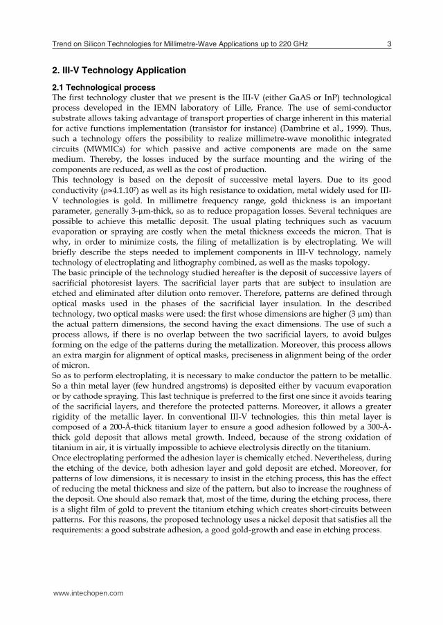
2.1 Technological process The first technology cluster that we present is the III-V (either GaAS or InP) technological process developed in the IEMN laboratory of Lille, France. The use of semi-conductor substrate allows taking advantage of transport properties of charge inherent in this material for active functions implementation (transistor for instance) (Dambrine et al., 1999). Thus, such a technology offers the possibility to realize millimetre-wave monolithic integrated circuits (MWMICs) for which passive and active components are made on the same medium. Thereby, the losses induced by the surface mounting and the wiring of the components are reduced, as well as the cost of production. This technology is based on the deposit of successive metal layers. Due to its good conductivity (4.1.107) as well as its high resistance to oxidation, metal widely used for III-V technologies is gold. In millimetre frequency range, gold thickness is an important parameter, generally 3-µm-thick, so as to reduce propagation losses. Several techniques are possible to achieve this metallic deposit. The usual plating techniques such as vacuum evaporation or spraying are costly when the metal thickness exceeds the micron. That is why, in order to minimize costs, the filing of metallization is by electroplating. We will briefly describe the steps needed to implement components in III-V technology, namely technology of electroplating and lithography combined, as well as the masks topology. The basic principle of the technology studied hereafter is the deposit of successive layers of sacrificial photoresist layers. The sacrificial layer parts that are subject to insulation are etched and eliminated after dilution onto remover. Therefore, patterns are defined through optical masks used in the phases of the sacrificial layer insulation. In the described technology, two optical masks were used: the first whose dimensions are higher (3 µm) than the actual pattern dimensions, the second having the exact dimensions. The use of such a process allows, if there is no overlap between the two sacrificial layers, to avoid bulges forming on the edge of the patterns during the metallization. Moreover, this process allows an extra margin for alignment of optical masks, preciseness in alignment being of the order of micron. So as to perform electroplating, it is necessary to make conductor the pattern to be metallic. So a thin metal layer (few hundred angstroms) is deposited either by vacuum evaporation or by cathode spraying. This last technique is preferred to the first one since it avoids tearing of the sacrificial layers, and therefore the protected patterns. Moreover, it allows a greater rigidity of the metallic layer. In conventional III-V technologies, this thin metal layer is composed of a 200-Å-thick titanium layer to ensure a good adhesion followed by a 300-Å-thick gold deposit that allows metal growth. Indeed, because of the strong oxidation of titanium in air, it is virtually impossible to achieve electrolysis directly on the titanium. Once electroplating performed the adhesion layer is chemically etched. Nevertheless, during the etching of the device, both adhesion layer and gold deposit are etched. Moreover, for patterns of low dimensions, it is necessary to insist in the etching process, this has the effect of reducing the metal thickness and size of the pattern, but also to increase the roughness of the deposit. One should also remark that, most of the time, during the etching process, there is a slight film of gold to prevent the titanium etching which creates short-circuits between patterns. For this reasons, the proposed technology uses a nickel deposit that satisfies all the requirements: a good substrate adhesion, a good gold-growth and ease in etching process.
www.intechopen.com
Trend on Silicon Technologies for Millimetre-Wave Applications up to 220 GHz 3
alternative to classical III-V technologies to address millimetre-wave applications. Moreover, next-generation silicon-based RF CMOS and BiCMOS technologies, which offer NMOS and SiGe HBT devices with cutoff frequencies beyond 277 GHz (Kuhn et al., 2004) and 300 GHz (Rieh et al., 2004) respectively, will enable the implementation of millimetre-wave system-on-chip (SoC) such as 60 GHz WLAN (Floyd et al., 2006),(Doan et al., 2004), 40/80/160 Gb/s optic-fiber transceivers (Perndl et al., 2004) or 24/77 GHz collision avoidance radars, which were reserved until recently to III-V compound semiconductors application domain. However, integration of high performances passive components remains a key issue in silicon technologies. Some of the available solutions consists in the use of silicon as a support for active function development, passive functions being implemented on silicon using specific technologies such as membrane technologies (Vu et al., 2008) or thin film microstrip (TFMS) based technologies developed on Si-BCB substrate (Six et al., 2006), (Prigent et al., 2004), (Wolf et al., 2005). Nevertheless, if such technologies have already proved their efficacy for sub-millimeter wave functions, their implementation remains difficult since they need complex technological process. Recent work (Gianesello et al., 2006) have demonstrated that silicon technologies are able to address higher frequencies applications up to G-band (140-220 GHz) if high resistivity (HR) silicon-on-insulator (SOI) technology is used. Moreover, feasibility of integrated antenna made on advanced CMOS standard technology has been demonstrated (Montusclat et al., 2005) and HR SOI technology has proved its efficacy to improve the overall performances of integrated antennas. However, in millimeter frequency range, the design of narrow-band planar filters appears as one of the most critical point. Hence, in view of the required selectivity levels, designers are, indeed, faced with problems in relation to control design, i.e. modelling accuracy, as well as the high insertion loss levels inherent in such devices. Moreover, due to low electrical lengths involved in millimetre-wave, the technological dispersion has to be as low as possible. This chapter is aimed at describing the evolution of technological processes for the design of passive functions in millimetre-wave frequency range. III-V technologies that are behind the development of millimetre-microwave functions in W-band are first described. Performances obtained in III-V technology for wide- and narrow-band filters reported here will be the reference for comparison with other technologies. Several technological process dedicated to silicon technologies were then studied: membrane and thin film microstrip technologies. Finally, millimetre-wave electrical performances of devices were reported for passive components and active circuits achieved in ST-Microelectronics advanced CMOS HR SOI technology, so as to investigate for the suitability of that technology to address millimetre-wave Systems on Chip (SOC) up to 220 GHz and beyond. Classical stub-based broadband filters implemented in coplanar waveguide technology were first designed so as to prove the technological process accuracy as well as its performances which are fully competitive with III-V technologies. Then, the design of coupled-lines narrowband filters was investigated in the V-band, at 60 GHz. These concepts were validated through comparison with experiments performed up to 220 GHz.
2. III-V Technology Application
2.1 Technological process The first technology cluster that we present is the III-V (either GaAS or InP) technological process developed in the IEMN laboratory of Lille, France. The use of semi-conductor substrate allows taking advantage of transport properties of charge inherent in this material for active functions implementation (transistor for instance) (Dambrine et al., 1999). Thus, such a technology offers the possibility to realize millimetre-wave monolithic integrated circuits (MWMICs) for which passive and active components are made on the same medium. Thereby, the losses induced by the surface mounting and the wiring of the components are reduced, as well as the cost of production. This technology is based on the deposit of successive metal layers. Due to its good conductivity (4.1.107) as well as its high resistance to oxidation, metal widely used for III-V technologies is gold. In millimetre frequency range, gold thickness is an important parameter, generally 3-µm-thick, so as to reduce propagation losses. Several techniques are possible to achieve this metallic deposit. The usual plating techniques such as vacuum evaporation or spraying are costly when the metal thickness exceeds the micron. That is why, in order to minimize costs, the filing of metallization is by electroplating. We will briefly describe the steps needed to implement components in III-V technology, namely technology of electroplating and lithography combined, as well as the masks topology. The basic principle of the technology studied hereafter is the deposit of successive layers of sacrificial photoresist layers. The sacrificial layer parts that are subject to insulation are etched and eliminated after dilution onto remover. Therefore, patterns are defined through optical masks used in the phases of the sacrificial layer insulation. In the described technology, two optical masks were used: the first whose dimensions are higher (3 µm) than the actual pattern dimensions, the second having the exact dimensions. The use of such a process allows, if there is no overlap between the two sacrificial layers, to avoid bulges forming on the edge of the patterns during the metallization. Moreover, this process allows an extra margin for alignment of optical masks, preciseness in alignment being of the order of micron. So as to perform electroplating, it is necessary to make conductor the pattern to be metallic. So a thin metal layer (few hundred angstroms) is deposited either by vacuum evaporation or by cathode spraying. This last technique is preferred to the first one since it avoids tearing of the sacrificial layers, and therefore the protected patterns. Moreover, it allows a greater rigidity of the metallic layer. In conventional III-V technologies, this thin metal layer is composed of a 200-Å-thick titanium layer to ensure a good adhesion followed by a 300-Å-thick gold deposit that allows metal growth. Indeed, because of the strong oxidation of titanium in air, it is virtually impossible to achieve electrolysis directly on the titanium. Once electroplating performed the adhesion layer is chemically etched. Nevertheless, during the etching of the device, both adhesion layer and gold deposit are etched. Moreover, for patterns of low dimensions, it is necessary to insist in the etching process, this has the effect of reducing the metal thickness and size of the pattern, but also to increase the roughness of the deposit. One should also remark that, most of the time, during the etching process, there is a slight film of gold to prevent the titanium etching which creates short-circuits between patterns. For this reasons, the proposed technology uses a nickel deposit that satisfies all the requirements: a good substrate adhesion, a good gold-growth and ease in etching process.
www.intechopen.com
Microwave and Millimeter Wave Technologies: from Photonic Bandgap Devices to Antenna and Applications 4
The third step consists in electroplating itself, once achieved patterns definition and thin metal layer deposit phases. An electric current flow in an electrolyte solution (solution of double cyanide of gold and potassium (KAu(CN)2)) creates a chemical reaction near electrodes. Gold ions being positive, the sample foil is attached to the cathode. It follows a phenomenon of transfer of charges called electroplating. This basic principle is relatively simple; however this operation must still be undertaken with some caution. Indeed, ohmic losses of a transmission line depend not only on the resistivity of the metal, but also to its surface state. But the roughness of the metallic layer increases with the current density. It is therefore necessary to apply a current density relatively low. However, if very low current density yields a very low roughness, it also increases the time of filing causing problems of mechanical strength of the sacrificial layer. We must therefore find a compromise between roughness and mechanical strength.
3 µm Gold electroplating
III-V Substrate
Thick Photoresist
Thin Photoresist Thin Metal Film
(a)
(b)
III-V Substrate
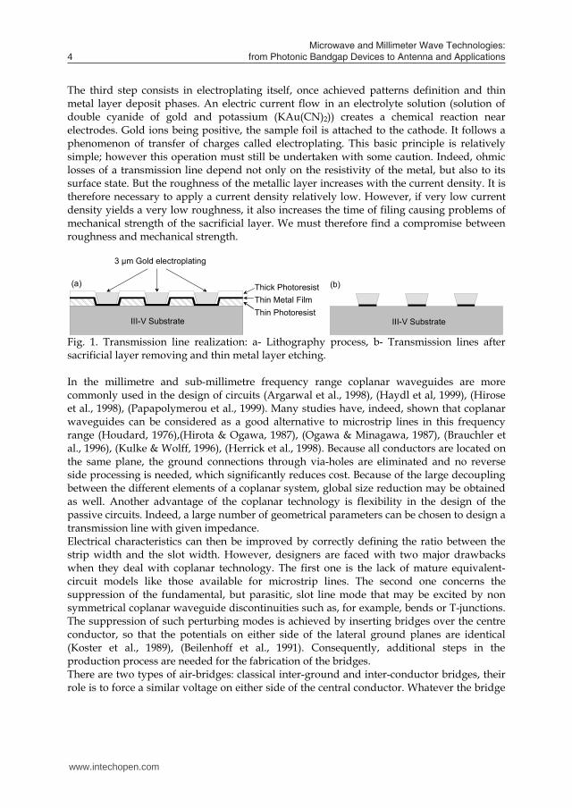
Fig. 1. Transmission line realization: a- Lithography process, b- Transmission lines after sacrificial layer removing and thin metal layer etching. In the millimetre and sub-millimetre frequency range coplanar waveguides are more commonly used in the design of circuits (Argarwal et al., 1998), (Haydl et al, 1999), (Hirose et al., 1998), (Papapolymerou et al., 1999). Many studies have, indeed, shown that coplanar waveguides can be considered as a good alternative to microstrip lines in this frequency range (Houdard, 1976),(Hirota & Ogawa, 1987), (Ogawa & Minagawa, 1987), (Brauchler et al., 1996), (Kulke & Wolff, 1996), (Herrick et al., 1998). Because all conductors are located on the same plane, the ground connections through via-holes are eliminated and no reverse side processing is needed, which significantly reduces cost. Because of the large decoupling between the different elements of a coplanar system, global size reduction may be obtained as well. Another advantage of the coplanar technology is flexibility in the design of the passive circuits. Indeed, a large number of geometrical parameters can be chosen to design a transmission line with given impedance. Electrical characteristics can then be improved by correctly defining the ratio between the strip width and the slot width. However, designers are faced with two major drawbacks when they deal with coplanar technology. The first one is the lack of mature equivalent-circuit models like those available for microstrip lines. The second one concerns the suppression of the fundamental, but parasitic, slot line mode that may be excited by non symmetrical coplanar waveguide discontinuities such as, for example, bends or T-junctions. The suppression of such perturbing modes is achieved by inserting bridges over the centre conductor, so that the potentials on either side of the lateral ground planes are identical (Koster et al., 1989), (Beilenhoff et al., 1991). Consequently, additional steps in the production process are needed for the fabrication of the bridges. There are two types of air-bridges: classical inter-ground and inter-conductor bridges, their role is to force a similar voltage on either side of the central conductor. Whatever the bridge
topology, the technological process for bridge realization is identical and similar to the technological process described above (Fig. 2). Besides the good definition for devices due to the high-resolution technology, one of the advantages of this technological process is the control of the shape of the air-bridge. Indeed in hybrid technology, air-bridges are generally implemented by using wire-bounding connected manually to the ground plane. By such a process the shape of the bridge is difficult to control involving a problem of reproducibility first and in the other hand problems with bridge modelling. Here, however, the technology used allows good control of the fixture of these bridges as illustrate in Fig. 2.
Substrat III-V
(b)
3 µm Gold electroplating
Thick Photoresist
Thin Metal Film
Thick Photoresist s = 22 m
w = 26 m
10 m
d = 70 m3 m
Fig. 2. Air-bridge realization: (a)- Lithography process, (b)- Airbridges realized with IEMN technological process. In order to minimize the parasitic influence of the bridge on the electrical characteristic of the lines and provide mechanical stability, the dimensions of the air bridge used are: 3 µm height, 10 µm width, 80 µm length (d=70 µm + 10 µm minimum spacing between slot border and bridge), and 3-µm metal thickness. Moreover, to give it a good mechanical stability, a maximum length must be defined for a given width: for example, 10 µm and 20 µm widths allow maximum lengths of 100 and 180 µm, respectively. Although the bridge introduces an excess capacitance, this does not constitute a problem for the bridge widths here as long as the strip widths of the coplanar line are all kept small. Under a configuration with these dimensions, no compensation techniques, such as using sections of high-impedance line, are required (Rius et al., 2000-a), (Weller et al., 1999).
2.2 Optimal dimensions for coplanar transmission lines So as to determine the optimum sizing of coplanar transmission lines, we rely on the work of W. Heinrich (Heinrich, 1993). The proposed quasi-TEM description ensued from a quasi-static approach. The RLCG equivalent circuit components are determined from approximate analytical equations derived from a global analysis. These values depend for electrical and geometrical parameter of the transmission lines as well as the frequency. C and G elements are considered invariant with frequency. However, as the skin effect modifies the current distribution in conductors depending on frequency, the R and L elements are highly dependant on frequency. For instance, let us consider a 50 coplanar transmission line implemented in GaAs technology (h=400 µm, t=3 µm, r=11.9, tan =210-4, =4.1107 S.m) with line- and slot-width of W=26 µm, S=22µm, respectively. Fig. 3 illustrates the evolution of the R and L parameter for transmission line model as a function of the frequency.
www.intechopen.com
Trend on Silicon Technologies for Millimetre-Wave Applications up to 220 GHz 5
The third step consists in electroplating itself, once achieved patterns definition and thin metal layer deposit phases. An electric current flow in an electrolyte solution (solution of double cyanide of gold and potassium (KAu(CN)2)) creates a chemical reaction near electrodes. Gold ions being positive, the sample foil is attached to the cathode. It follows a phenomenon of transfer of charges called electroplating. This basic principle is relatively simple; however this operation must still be undertaken with some caution. Indeed, ohmic losses of a transmission line depend not only on the resistivity of the metal, but also to its surface state. But the roughness of the metallic layer increases with the current density. It is therefore necessary to apply a current density relatively low. However, if very low current density yields a very low roughness, it also increases the time of filing causing problems of mechanical strength of the sacrificial layer. We must therefore find a compromise between roughness and mechanical strength.
3 µm Gold electroplating
III-V Substrate
Thick Photoresist
Thin Photoresist Thin Metal Film
(a)
(b)
III-V Substrate
Fig. 1. Transmission line realization: a- Lithography process, b- Transmission lines after sacrificial layer removing and thin metal layer etching. In the millimetre and sub-millimetre frequency range coplanar waveguides are more commonly used in the design of circuits (Argarwal et al., 1998), (Haydl et al, 1999), (Hirose et al., 1998), (Papapolymerou et al., 1999). Many studies have, indeed, shown that coplanar waveguides can be considered as a good alternative to microstrip lines in this frequency range (Houdard, 1976),(Hirota & Ogawa, 1987), (Ogawa & Minagawa, 1987), (Brauchler et al., 1996), (Kulke & Wolff, 1996), (Herrick et al., 1998). Because all conductors are located on the same plane, the ground connections through via-holes are eliminated and no reverse side processing is needed, which significantly reduces cost. Because of the large decoupling between the different elements of a coplanar system, global size reduction may be obtained as well. Another advantage of the coplanar technology is flexibility in the design of the passive circuits. Indeed, a large number of geometrical parameters can be chosen to design a transmission line with given impedance. Electrical characteristics can then be improved by correctly defining the ratio between the strip width and the slot width. However, designers are faced with two major drawbacks when they deal with coplanar technology. The first one is the lack of mature equivalent-circuit models like those available for microstrip lines. The second one concerns the suppression of the fundamental, but parasitic, slot line mode that may be excited by non symmetrical coplanar waveguide discontinuities such as, for example, bends or T-junctions. The suppression of such perturbing modes is achieved by inserting bridges over the centre conductor, so that the potentials on either side of the lateral ground planes are identical (Koster et al., 1989), (Beilenhoff et al., 1991). Consequently, additional steps in the production process are needed for the fabrication of the bridges. There are two types of air-bridges: classical inter-ground and inter-conductor bridges, their role is to force a similar voltage on either side of the central conductor. Whatever the bridge
topology, the technological process for bridge realization is identical and similar to the technological process described above (Fig. 2). Besides the good definition for devices due to the high-resolution technology, one of the advantages of this technological process is the control of the shape of the air-bridge. Indeed in hybrid technology, air-bridges are generally implemented by using wire-bounding connected manually to the ground plane. By such a process the shape of the bridge is difficult to control involving a problem of reproducibility first and in the other hand problems with bridge modelling. Here, however, the technology used allows good control of the fixture of these bridges as illustrate in Fig. 2.
Substrat III-V
(b)
3 µm Gold electroplating
Thick Photoresist
Thin Metal Film
Thick Photoresist s = 22 m
w = 26 m
10 m
d = 70 m3 m
Fig. 2. Air-bridge realization: (a)- Lithography process, (b)- Airbridges realized with IEMN technological process. In order to minimize the parasitic influence of the bridge on the electrical characteristic of the lines and provide mechanical stability, the dimensions of the air bridge used are: 3 µm height, 10 µm width, 80 µm length (d=70 µm + 10 µm minimum spacing between slot border and bridge), and 3-µm metal thickness. Moreover, to give it a good mechanical stability, a maximum length must be defined for a given width: for example, 10 µm and 20 µm widths allow maximum lengths of 100 and 180 µm, respectively. Although the bridge introduces an excess capacitance, this does not constitute a problem for the bridge widths here as long as the strip widths of the coplanar line are all kept small. Under a configuration with these dimensions, no compensation techniques, such as using sections of high-impedance line, are required (Rius et al., 2000-a), (Weller et al., 1999).
2.2 Optimal dimensions for coplanar transmission lines So as to determine the optimum sizing of coplanar transmission lines, we rely on the work of W. Heinrich (Heinrich, 1993). The proposed quasi-TEM description ensued from a quasi-static approach. The RLCG equivalent circuit components are determined from approximate analytical equations derived from a global analysis. These values depend for electrical and geometrical parameter of the transmission lines as well as the frequency. C and G elements are considered invariant with frequency. However, as the skin effect modifies the current distribution in conductors depending on frequency, the R and L elements are highly dependant on frequency. For instance, let us consider a 50 coplanar transmission line implemented in GaAs technology (h=400 µm, t=3 µm, r=11.9, tan =210-4, =4.1107 S.m) with line- and slot-width of W=26 µm, S=22µm, respectively. Fig. 3 illustrates the evolution of the R and L parameter for transmission line model as a function of the frequency.
www.intechopen.com
Microwave and Millimeter Wave Technologies: from Photonic Bandgap Devices to Antenna and Applications 6
With knowledge of RLCG parameters, one can easily determine the parameters of propagation, attenuation, impedance and effective permittivity and, therefore optimal rules for transmission line sizing as a function of its geometrical parameters: line- and slot-widths as well as ground-to-ground distance. The inter-ground distance (d=W+2S) is an important parameter for wave propagation. Indeed, so as to avoid propagation of parasitic modes, this distance d has to be low compared to the wavelength; the commonly used constraint is d g/10. An increase of this constraint (d g/20=dmax) allows neglecting the radiation losses. Moreover, it limits extend of radiating waves, and therefore the problems relied to packaging. However, according to Fig. 4-(a), the attenuation also depends on the ground-to-ground distance. It is, in fact, inversely proportional to the distance d. It follows that inter-ground distance d must be the closest to dmax. Once the inter-ground distance chosen, we are interested in the relation between the dimensions of the line-width and inter-ground distance. This ration W/d is predominant in the choice of the achievable characteristic impedances. According to Fig. 4-(b) so as to limit the attenuation, it is preferable to set W in the interval between 0.3d and 0.6d. Moreover, the ground plane width (Wg) and the substrate thickness (hs) are chosen to make a trade-off between losses and low dispersion up to the W-frequency band. To summarize, the following conditions are then chosen to realize our devices:
10-2
10-1
100
101
102
10-1
100
101
frequency (GHz)
R (O
hm/m
m)
10-2
10-1
100
101
102
0.4
0.45
0.5
0.55
0.6
0.65
frequency (GHz)
L (n
H/m
m)
Fig. 3. Evolution of R and L parameters as a function of the frequency.
maxg dSWd
202
(1)
d.Wd. 6030 (2) SWWg 2 (3) SWhs 22 (4)
101
102
103
10-2
10-1
100
d (µm)
Atte
nuat
ion
(dB
/mm
)
(a)
0.2 0.4 0.6 0.80.05
0.1
0.15
0.2
0.25
0.3
W/d
Atte
nuat
ion
(dB
/mm
)
(b)
f=40 GHzf=60 GHzf=77 GHzf=94 GHzf=110 GHz
Fig. 4. Evolution of the attenuation as a function of : (a) ground-to-ground distance. (b) Line width (W) to ground-to ground (d) ration.
2.3 Wide-band bandpass filter design We first investigated on the design of quarter-wavelength shunt-stub filters. Such topology includes shorted stubs as resonators separated by quarter-wavelength transmission lines as inverters. The synthesis developed by Matthaei (Matthaei et al., 1980) indicates that the bandwidth is in close relation with the impedance level of the resonators. In the present case, so as to respect optimal sizing described above the impedance range extends from 30 to 70 . Thus, the available 3-dB bandwidth will be approximately bounded by 100% and 36%. For bandwidths below 36%, very low impedance levels are needed. Thus, shape factors become too large for correct performance from the device with regard to both the parasitic influences of the discontinuities and modelling difficulties. So, other topologies such as coupled-line filters are preferred. The first results presented here deal with 58% and 36%, 3-dB-bandwidth, 3rd-order filters centred on 82.7 GHz. According to synthesis, the first example with 58% 3-dB-bandwidth results in a 25 impedance for the resonators when inverters are kept to 51 . Twenty-five is chosen so as to introduce double 50 stubs for the resonator (Fig. 5-(a)). According to the low level of insertion losses, the standard geometry was chosen as follows: 26 µm for the strip widths and 22 µm for the slot widths. The 36% bandwidth was reached by selecting impedances of 56 and 15 for inverters and resonators, respectively. As before, 15 was obtained with two double 30 stubs. It corresponds to the lowest bandwidth that can be reached with an impedance range bounded by 30 and 70. For the inverters, strips and slots were 20 µm and 25 µm, respectively, and 54 µm and 8 µm for the resonators. The layout and frequency response are displayed in Fig. 5-(b). As for the first prototype, experimental and simulated results agree over a broad-band frequency.
www.intechopen.com
Trend on Silicon Technologies for Millimetre-Wave Applications up to 220 GHz 7
With knowledge of RLCG parameters, one can easily determine the parameters of propagation, attenuation, impedance and effective permittivity and, therefore optimal rules for transmission line sizing as a function of its geometrical parameters: line- and slot-widths as well as ground-to-ground distance. The inter-ground distance (d=W+2S) is an important parameter for wave propagation. Indeed, so as to avoid propagation of parasitic modes, this distance d has to be low compared to the wavelength; the commonly used constraint is d g/10. An increase of this constraint (d g/20=dmax) allows neglecting the radiation losses. Moreover, it limits extend of radiating waves, and therefore the problems relied to packaging. However, according to Fig. 4-(a), the attenuation also depends on the ground-to-ground distance. It is, in fact, inversely proportional to the distance d. It follows that inter-ground distance d must be the closest to dmax. Once the inter-ground distance chosen, we are interested in the relation between the dimensions of the line-width and inter-ground distance. This ration W/d is predominant in the choice of the achievable characteristic impedances. According to Fig. 4-(b) so as to limit the attenuation, it is preferable to set W in the interval between 0.3d and 0.6d. Moreover, the ground plane width (Wg) and the substrate thickness (hs) are chosen to make a trade-off between losses and low dispersion up to the W-frequency band. To summarize, the following conditions are then chosen to realize our devices:
10-2
10-1
100
101
102
10-1
100
101
frequency (GHz)
R (O
hm/m
m)
10-2
10-1
100
101
102
0.4
0.45
0.5
0.55
0.6
0.65
frequency (GHz)
L (n
H/m
m)
Fig. 3. Evolution of R and L parameters as a function of the frequency.
maxg dSWd
202
(1)
d.Wd. 6030 (2) SWWg 2 (3) SWhs 22 (4)
101
102
103
10-2
10-1
100
d (µm)
Atte
nuat
ion
(dB
/mm
)
(a)
0.2 0.4 0.6 0.80.05
0.1
0.15
0.2
0.25
0.3
W/d
Atte
nuat
ion
(dB
/mm
)
(b)
f=40 GHzf=60 GHzf=77 GHzf=94 GHzf=110 GHz
Fig. 4. Evolution of the attenuation as a function of : (a) ground-to-ground distance. (b) Line width (W) to ground-to ground (d) ration.
2.3 Wide-band bandpass filter design We first investigated on the design of quarter-wavelength shunt-stub filters. Such topology includes shorted stubs as resonators separated by quarter-wavelength transmission lines as inverters. The synthesis developed by Matthaei (Matthaei et al., 1980) indicates that the bandwidth is in close relation with the impedance level of the resonators. In the present case, so as to respect optimal sizing described above the impedance range extends from 30 to 70 . Thus, the available 3-dB bandwidth will be approximately bounded by 100% and 36%. For bandwidths below 36%, very low impedance levels are needed. Thus, shape factors become too large for correct performance from the device with regard to both the parasitic influences of the discontinuities and modelling difficulties. So, other topologies such as coupled-line filters are preferred. The first results presented here deal with 58% and 36%, 3-dB-bandwidth, 3rd-order filters centred on 82.7 GHz. According to synthesis, the first example with 58% 3-dB-bandwidth results in a 25 impedance for the resonators when inverters are kept to 51 . Twenty-five is chosen so as to introduce double 50 stubs for the resonator (Fig. 5-(a)). According to the low level of insertion losses, the standard geometry was chosen as follows: 26 µm for the strip widths and 22 µm for the slot widths. The 36% bandwidth was reached by selecting impedances of 56 and 15 for inverters and resonators, respectively. As before, 15 was obtained with two double 30 stubs. It corresponds to the lowest bandwidth that can be reached with an impedance range bounded by 30 and 70. For the inverters, strips and slots were 20 µm and 25 µm, respectively, and 54 µm and 8 µm for the resonators. The layout and frequency response are displayed in Fig. 5-(b). As for the first prototype, experimental and simulated results agree over a broad-band frequency.
www.intechopen.com
Microwave and Millimeter Wave Technologies: from Photonic Bandgap Devices to Antenna and Applications 8
0 1 1 2 2 3 3 4 4 5 5 6 6 7 7 8 8 1 1 09 9
0
-1 0
-2 0
-3 0
-4 0
-5 0
F R E Q U E N C Y (G H z )
dB
(S2
1)
dB
(S1
1)
F1=82.70 GHzS21= -0.967 dB
Simulated resultsExperimental results
F1
F2
F2=74.00 GHzS11= -18.09 dB
2 0 0 µ m
F1=82.70 GHzS21= -1.81 dB
F2=87.60GHzS11= -20.81 dB
Simulated resultsExperimental results
F1
F2
2 0 0 µ m
0 1 1 2 2 3 3 4 4 5 5 6 6 7 7 8 8 1 1 09 9
0
-1 0
-2 0
-3 0
-4 0
-5 0
F R E Q U E N C Y (G H z )
dB
(S2
1)
dB
(S1
1)
(a) (b)
Fig. 5. Layout, simulated, and experimental associated magnitude responses of the 82.7-GHz central-frequency, (a) 58% 3-dB-bandwidth and (b) 36% 3-dB-bandwidth filters. As shown in Fig. 5, insertion losses increase with filter selectivity: 0.96, and 1.81 dB are obtained for 58%, and 36% bandwidth filters, respectively. These values are in complete agreement with the following expression (Matthaei et al., 1980), (Cohn, 1959):
wQn..L.I
u 3434 (5)
with I.L. the insertion loss in decibels, n the filter order, w its relative bandwidth, and Qu the unloaded quality factor, which is close to 25 for the standard 50 transmission line used here.
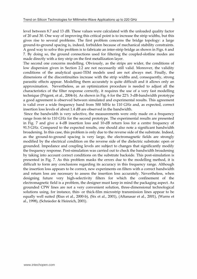
2.5 Narrow-band bandpass filter design Two major problems are related to narrow-band bandpass coupled-lines filters. First, insertion losses become important when the selectivity of the filter is increased. The second problem deals with accuracy which is directly in relation to the level of selectivity. In order to illustrate this, we present the results obtained with two classical coupled-lines third-order bandpass filters. The first one is at a center frequency of 65 GHz, 22% 3-dB bandwidth whereas the second one is at 94 GHz, 5% 3-dB bandwidth. Figs. 6 and 7 show the layouts of these filters. For such topologies, according to well-known synthesis (Matthaei et al., 1980), the bandwidth and the coupling coefficient level of the coupled-lines sections are in close relation. Indeed, narrow selective bandwidths are obtained with low coupling levels on the central sections of the filter. A convenient solution consists of using a separating ground plane between the coupled strips. This leads to low coupling levels on a reduced bulk and this separate ground plane acts as a good parasitic mode filter (Fig. 7). According to the finite conductivity of the metal (4.1107 S.m for gold metallization) and to the dissipation factor of the GaAs substrate (tan=210-4), very high insertion losses are expected when designing such narrow-band filters. These insertion losses can be predicted roughly from (5). For instance, for a third-order, 22% 3-dB-bandwidth coupled-line filter designed with 26-µm strip widths, insertion losses between 1.95 dB and 2.95 dB are obtained. However, if the bandwidth is decreased to 5%, insertion losses reach a critical
level between 8.7 and 13 dB. These values were calculated with the unloaded quality factor of 20 and 30. One way of improving this critical point is to increase the strip widths, but this gives rise to several problems. The first problem concerns the bridge topology: a large ground-to-ground spacing is, indeed, forbidden because of mechanical stability constraints. A good way to solve this problem is to fabricate an inter-strip bridge as shown in Figs. 6 and 7. By doing so, the ground connections used for filtering the coupled-slotline modes are made directly with a tiny strip on the first metallization layer. The second one concerns modelling. Obviously, as the strips are wider, the conditions of low dispersion given in Section 2.2 are not necessarily still valid. Moreover, the validity conditions of the analytical quasi-TEM models used are not always met. Finally, the dimensions of the discontinuities increase with the strip widths and, consequently, strong parasitic effects appear. Modelling them accurately is quite difficult and it allows only an approximation. Nevertheless, as an optimization procedure is needed to adjust all the characteristics of the filter response correctly, it requires the use of a very fast modelling technique (Prigent, et al., 2004-b). As shown in Fig. 6 for the 22% 3-dB-bandwidth prototypea good agreement is observed between simulated and experimental results. This agreement is valid over a wide frequency band from 500 MHz to 110 GHz and, as expected, correct insertion loss levels of about 1.4 dB are observed in the bandwidth. Since the bandwidth is very selective, the measurements were only made on a frequency range from 66 to 110 GHz for the second prototype. The experimental results are presented in Fig. 7 and give a 4-dB insertion loss and 10-dB return loss for a centre frequency of 91.5 GHz. Compared to the expected results, one should also note a significant bandwidth broadening. In this case, this problem is only due to the reverse side of the substrate. Indeed, as the ground-to-ground spacing is very large, the electromagnetic fields are strongly modified by the electrical condition on the reverse side of the dielectric substrate: open or grounded. Impedance and coupling levels are subject to changes that significantly modify the frequency response. Post-simulation was carried out to check the bandwidth broadening by taking into account correct conditions on the substrate backside. This post-simulation is presented in Fig. 7. As this problem masks the errors due to the modelling method, it is difficult to form any conclusions regarding its accuracy in this frequency range. Although the insertion loss appears to be correct, new experiments on filters with a correct bandwidth and return loss are necessary to assess the insertion loss accurately. Nevertheless, when designing future very high-selectivity filters for which the confinement of the electromagnetic field is a problem, the designer must keep in mind the packaging aspect. As grounded CPW lines are not a very convenient solution, three-dimensional technological solutions using, for instance, thin- or thick-film microstrip transmission lines appear to be equally well suited (Rius et al., 2000-b), (Six et al., 2001), (Aftanasar et al., 2001), (Warns et al., 1998), (Schnieder & Heinrich, 2001).
www.intechopen.com
Trend on Silicon Technologies for Millimetre-Wave Applications up to 220 GHz 9
0 1 1 2 2 3 3 4 4 5 5 6 6 7 7 8 8 1 1 09 9
0
-1 0
-2 0
-3 0
-4 0
-5 0
F R E Q U E N C Y (G H z )
dB
(S2
1)
dB
(S1
1)
F1=82.70 GHzS21= -0.967 dB
Simulated resultsExperimental results
F1
F2
F2=74.00 GHzS11= -18.09 dB
2 0 0 µ m
F1=82.70 GHzS21= -1.81 dB
F2=87.60GHzS11= -20.81 dB
Simulated resultsExperimental results
F1
F2
2 0 0 µ m
0 1 1 2 2 3 3 4 4 5 5 6 6 7 7 8 8 1 1 09 9
0
-1 0
-2 0
-3 0
-4 0
-5 0
F R E Q U E N C Y (G H z )
dB
(S2
1)
dB
(S1
1)
(a) (b)
Fig. 5. Layout, simulated, and experimental associated magnitude responses of the 82.7-GHz central-frequency, (a) 58% 3-dB-bandwidth and (b) 36% 3-dB-bandwidth filters. As shown in Fig. 5, insertion losses increase with filter selectivity: 0.96, and 1.81 dB are obtained for 58%, and 36% bandwidth filters, respectively. These values are in complete agreement with the following expression (Matthaei et al., 1980), (Cohn, 1959):
wQn..L.I
u 3434 (5)
with I.L. the insertion loss in decibels, n the filter order, w its relative bandwidth, and Qu the unloaded quality factor, which is close to 25 for the standard 50 transmission line used here.
2.5 Narrow-band bandpass filter design Two major problems are related to narrow-band bandpass coupled-lines filters. First, insertion losses become important when the selectivity of the filter is increased. The second problem deals with accuracy which is directly in relation to the level of selectivity. In order to illustrate this, we present the results obtained with two classical coupled-lines third-order bandpass filters. The first one is at a center frequency of 65 GHz, 22% 3-dB bandwidth whereas the second one is at 94 GHz, 5% 3-dB bandwidth. Figs. 6 and 7 show the layouts of these filters. For such topologies, according to well-known synthesis (Matthaei et al., 1980), the bandwidth and the coupling coefficient level of the coupled-lines sections are in close relation. Indeed, narrow selective bandwidths are obtained with low coupling levels on the central sections of the filter. A convenient solution consists of using a separating ground plane between the coupled strips. This leads to low coupling levels on a reduced bulk and this separate ground plane acts as a good parasitic mode filter (Fig. 7). According to the finite conductivity of the metal (4.1107 S.m for gold metallization) and to the dissipation factor of the GaAs substrate (tan=210-4), very high insertion losses are expected when designing such narrow-band filters. These insertion losses can be predicted roughly from (5). For instance, for a third-order, 22% 3-dB-bandwidth coupled-line filter designed with 26-µm strip widths, insertion losses between 1.95 dB and 2.95 dB are obtained. However, if the bandwidth is decreased to 5%, insertion losses reach a critical
level between 8.7 and 13 dB. These values were calculated with the unloaded quality factor of 20 and 30. One way of improving this critical point is to increase the strip widths, but this gives rise to several problems. The first problem concerns the bridge topology: a large ground-to-ground spacing is, indeed, forbidden because of mechanical stability constraints. A good way to solve this problem is to fabricate an inter-strip bridge as shown in Figs. 6 and 7. By doing so, the ground connections used for filtering the coupled-slotline modes are made directly with a tiny strip on the first metallization layer. The second one concerns modelling. Obviously, as the strips are wider, the conditions of low dispersion given in Section 2.2 are not necessarily still valid. Moreover, the validity conditions of the analytical quasi-TEM models used are not always met. Finally, the dimensions of the discontinuities increase with the strip widths and, consequently, strong parasitic effects appear. Modelling them accurately is quite difficult and it allows only an approximation. Nevertheless, as an optimization procedure is needed to adjust all the characteristics of the filter response correctly, it requires the use of a very fast modelling technique (Prigent, et al., 2004-b). As shown in Fig. 6 for the 22% 3-dB-bandwidth prototypea good agreement is observed between simulated and experimental results. This agreement is valid over a wide frequency band from 500 MHz to 110 GHz and, as expected, correct insertion loss levels of about 1.4 dB are observed in the bandwidth. Since the bandwidth is very selective, the measurements were only made on a frequency range from 66 to 110 GHz for the second prototype. The experimental results are presented in Fig. 7 and give a 4-dB insertion loss and 10-dB return loss for a centre frequency of 91.5 GHz. Compared to the expected results, one should also note a significant bandwidth broadening. In this case, this problem is only due to the reverse side of the substrate. Indeed, as the ground-to-ground spacing is very large, the electromagnetic fields are strongly modified by the electrical condition on the reverse side of the dielectric substrate: open or grounded. Impedance and coupling levels are subject to changes that significantly modify the frequency response. Post-simulation was carried out to check the bandwidth broadening by taking into account correct conditions on the substrate backside. This post-simulation is presented in Fig. 7. As this problem masks the errors due to the modelling method, it is difficult to form any conclusions regarding its accuracy in this frequency range. Although the insertion loss appears to be correct, new experiments on filters with a correct bandwidth and return loss are necessary to assess the insertion loss accurately. Nevertheless, when designing future very high-selectivity filters for which the confinement of the electromagnetic field is a problem, the designer must keep in mind the packaging aspect. As grounded CPW lines are not a very convenient solution, three-dimensional technological solutions using, for instance, thin- or thick-film microstrip transmission lines appear to be equally well suited (Rius et al., 2000-b), (Six et al., 2001), (Aftanasar et al., 2001), (Warns et al., 1998), (Schnieder & Heinrich, 2001).
www.intechopen.com
Microwave and Millimeter Wave Technologies: from Photonic Bandgap Devices to Antenna and Applications 10
F1= 65.25 GHzS21= -1.461 dB
Simulated resultsExperimental results
0 1 1 2 2 3 3 4 4 5 5 6 6 7 7 8 8 1 1 09 9
0
-1 0
-2 0
-3 0
-4 0
-5 0
F R E Q U E N C Y (G H z )
dB
(S2
1)
dB
(S1
1)
Fig. 6. Layout, Simulated and experimental resuslts of a 65-GHz central-frequency, 22% 3-dB-bandwidth, coupled-line filter.
6 6 7 0 7 4 7 8 8 2 8 6 9 0 9 4 9 8 1 1 01 0 2
F1= 91.48 GHz
S21= -4.14 dB
F2= 94.78 GHzS11= -10.08 dB
Simulated resultsExperimental results
F1
F2
1 0 6
0
-1 0
-2 0
-3 0
-4 0
-5 0
F R E Q U E N C Y (G H z )
dB
(S2
1)
dB
(S1
1)
Fig. 7. Layout, Simulated and experimental resuslts of a 65-GHz central-frequency, 5% 3-dB-bandwidth, coupled-line filter.
3. Membrane Technologies
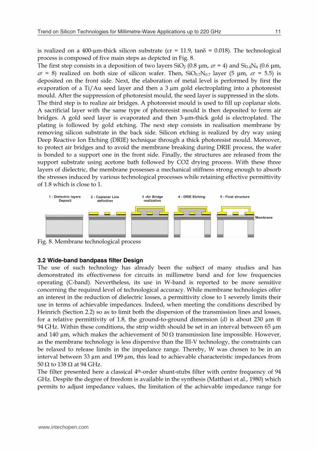
3.1 Technological process Contrary to the previously described III-V technologies which production cost limits their use to little series, technologies on silicon offer an interest with respect to cost reduction while retaining their interest in the integration of active functions. Nevertheless their major drawback is that levels of dielectric losses are not compatible with the specifications required for the passive functions. An alternative consists in the use of silicon membrane technology whose primary function is to mechanically support circuits while remaining transparent for functions in microwave. Thus, the electrical characteristics of this support match with those of vacuum, the ideal dielectric. On the other hand, membrane technology permits to minimize phenomena of dispersion, as well as the removal of cavity modes. The technological process developed here is nearly the same as the one developed in III-V technology. The major difference is the membrane realization and the backside etching of the silicon. The membrane technology developed at the LAAS laboratory (Toulouse, France)
is realized on a 400-µm-thick silicon substrate (r = 11.9, tan = 0.018). The technological process is composed of five main steps as depicted in Fig. 8. The first step consists in a deposition of two layers SiO2 (0.8 μm, r = 4) and Si3.4N4 (0.6 μm, r = 8) realized on both size of silicon wafer. Then, SiO0.7N0.7 layer (5 μm, r = 5.5) is deposited on the front side. Next, the elaboration of metal level is performed by first the evaporation of a Ti/Au seed layer and then a 3 µm gold electroplating into a photoresist mould. After the suppression of photoresist mould, the seed layer is suppressed in the slots. The third step is to realize air bridges. A photoresist mould is used to fill up coplanar slots. A sacrificial layer with the same type of photoresist mould is then deposited to form air bridges. A gold seed layer is evaporated and then 3-µm-thick gold is electroplated. The plating is followed by gold etching. The next step consists in realisation membrane by removing silicon substrate in the back side. Silicon etching is realized by dry way using Deep Reactive Ion Etching (DRIE) technique through a thick photoresist mould. Moreover, to protect air bridges and to avoid the membrane breaking during DRIE process, the wafer is bonded to a support one in the front side. Finally, the structures are released from the support substrate using acetone bath followed by CO2 drying process. With these three layers of dielectric, the membrane possesses a mechanical stiffness strong enough to absorb the stresses induced by various technological processes while retaining effective permittivity of 1.8 which is close to 1.
1 - Dielectric layers Deposit
2 - Coplanar Linedefinition
3 -Air Bridgerealization
4 - DRIE Etching 5 - Final structure
Membrane
Fig. 8. Membrane technological process
3.2 Wide-band bandpass filter Design The use of such technology has already been the subject of many studies and has demonstrated its effectiveness for circuits in millimetre band and for low frequencies operating (C-band). Nevertheless, its use in W-band is reported to be more sensitive concerning the required level of technological accuracy. While membrane technologies offer an interest in the reduction of dielectric losses, a permittivity close to 1 severely limits their use in terms of achievable impedances. Indeed, when meeting the conditions described by Heinrich (Section 2.2) so as to limit both the dispersion of the transmission lines and losses, for a relative permittivity of 1.8, the ground-to-ground dimension (d) is about 230 µm @ 94 GHz. Within these conditions, the strip width should be set in an interval between 65 µm and 140 µm, which makes the achievement of 50 transmission line impossible. However, as the membrane technology is less dispersive than the III-V technology, the constraints can be relaxed to release limits in the impedance range. Thereby, W was chosen to be in an interval between 33 µm and 199 µm, this lead to achievable characteristic impedances from 50 to 138 at 94 GHz. The filter presented here a classical 4th-order shunt-stubs filter with centre frequency of 94 GHz. Despite the degree of freedom is available in the synthesis (Matthaei et al., 1980) which permits to adjust impedance values, the limitation of the achievable impedance range for
www.intechopen.com
Trend on Silicon Technologies for Millimetre-Wave Applications up to 220 GHz 11
F1= 65.25 GHzS21= -1.461 dB
Simulated resultsExperimental results
0 1 1 2 2 3 3 4 4 5 5 6 6 7 7 8 8 1 1 09 9
0
-1 0
-2 0
-3 0
-4 0
-5 0
F R E Q U E N C Y (G H z )
dB
(S2
1)
dB
(S1
1)
Fig. 6. Layout, Simulated and experimental resuslts of a 65-GHz central-frequency, 22% 3-dB-bandwidth, coupled-line filter.
6 6 7 0 7 4 7 8 8 2 8 6 9 0 9 4 9 8 1 1 01 0 2
F1= 91.48 GHz
S21= -4.14 dB
F2= 94.78 GHzS11= -10.08 dB
Simulated resultsExperimental results
F1
F2
1 0 6
0
-1 0
-2 0
-3 0
-4 0
-5 0
F R E Q U E N C Y (G H z )
dB
(S2
1)
dB
(S1
1)
Fig. 7. Layout, Simulated and experimental resuslts of a 65-GHz central-frequency, 5% 3-dB-bandwidth, coupled-line filter.
3. Membrane Technologies
3.1 Technological process Contrary to the previously described III-V technologies which production cost limits their use to little series, technologies on silicon offer an interest with respect to cost reduction while retaining their interest in the integration of active functions. Nevertheless their major drawback is that levels of dielectric losses are not compatible with the specifications required for the passive functions. An alternative consists in the use of silicon membrane technology whose primary function is to mechanically support circuits while remaining transparent for functions in microwave. Thus, the electrical characteristics of this support match with those of vacuum, the ideal dielectric. On the other hand, membrane technology permits to minimize phenomena of dispersion, as well as the removal of cavity modes. The technological process developed here is nearly the same as the one developed in III-V technology. The major difference is the membrane realization and the backside etching of the silicon. The membrane technology developed at the LAAS laboratory (Toulouse, France)
is realized on a 400-µm-thick silicon substrate (r = 11.9, tan = 0.018). The technological process is composed of five main steps as depicted in Fig. 8. The first step consists in a deposition of two layers SiO2 (0.8 μm, r = 4) and Si3.4N4 (0.6 μm, r = 8) realized on both size of silicon wafer. Then, SiO0.7N0.7 layer (5 μm, r = 5.5) is deposited on the front side. Next, the elaboration of metal level is performed by first the evaporation of a Ti/Au seed layer and then a 3 µm gold electroplating into a photoresist mould. After the suppression of photoresist mould, the seed layer is suppressed in the slots. The third step is to realize air bridges. A photoresist mould is used to fill up coplanar slots. A sacrificial layer with the same type of photoresist mould is then deposited to form air bridges. A gold seed layer is evaporated and then 3-µm-thick gold is electroplated. The plating is followed by gold etching. The next step consists in realisation membrane by removing silicon substrate in the back side. Silicon etching is realized by dry way using Deep Reactive Ion Etching (DRIE) technique through a thick photoresist mould. Moreover, to protect air bridges and to avoid the membrane breaking during DRIE process, the wafer is bonded to a support one in the front side. Finally, the structures are released from the support substrate using acetone bath followed by CO2 drying process. With these three layers of dielectric, the membrane possesses a mechanical stiffness strong enough to absorb the stresses induced by various technological processes while retaining effective permittivity of 1.8 which is close to 1.
1 - Dielectric layers Deposit
2 - Coplanar Linedefinition
3 -Air Bridgerealization
4 - DRIE Etching 5 - Final structure
Membrane
Fig. 8. Membrane technological process
3.2 Wide-band bandpass filter Design The use of such technology has already been the subject of many studies and has demonstrated its effectiveness for circuits in millimetre band and for low frequencies operating (C-band). Nevertheless, its use in W-band is reported to be more sensitive concerning the required level of technological accuracy. While membrane technologies offer an interest in the reduction of dielectric losses, a permittivity close to 1 severely limits their use in terms of achievable impedances. Indeed, when meeting the conditions described by Heinrich (Section 2.2) so as to limit both the dispersion of the transmission lines and losses, for a relative permittivity of 1.8, the ground-to-ground dimension (d) is about 230 µm @ 94 GHz. Within these conditions, the strip width should be set in an interval between 65 µm and 140 µm, which makes the achievement of 50 transmission line impossible. However, as the membrane technology is less dispersive than the III-V technology, the constraints can be relaxed to release limits in the impedance range. Thereby, W was chosen to be in an interval between 33 µm and 199 µm, this lead to achievable characteristic impedances from 50 to 138 at 94 GHz. The filter presented here a classical 4th-order shunt-stubs filter with centre frequency of 94 GHz. Despite the degree of freedom is available in the synthesis (Matthaei et al., 1980) which permits to adjust impedance values, the limitation of the achievable impedance range for
www.intechopen.com
Microwave and Millimeter Wave Technologies: from Photonic Bandgap Devices to Antenna and Applications 12
membrane technologies does not allow us to reach bandwidth less than 55%. Nevertheless, the use of topology with dual stubs allows us to achieve narrower bandwidth. The layout of a 4th-order filter with dual short-ended stubs at 94 GHz is displayed in Fig. 9-(a). An insertion loss of 2 dB for a relative bandwidth of 45% is obtained by electromagnetic simulation HFSS (Fig. 9-(b)). Experimental results were made from 60 GHz to 110 GHz.
1847µm
2718 µm
21 3 4
1' 3' 4'
12 23 34
60 70 80 90 100 110 120 130
0
-10
-20
-30
-50
-40S11
(dB
), S2
1(dB
)FREQUENCY (GHz)
f0=94 GHzdB(S21)=-2.06
f0=93.38 GHzdB(S21)=-2.02
SIMULATION EXPERIMENT
(a) (b)
Fig. 9. 4th-ordre classical shunt-stubs bandpass filter. Photograph (a), Simulated and experimental magnitude responses (b) Based on the previous filter topology, we have developed a 4th-order filter with folded stubs in short-circuit termination. The benefit of such a structure is to promote a coupling between non-adjacent resonators. Thus, it creates a transmission zero whose frequency depends on the nature of the coupling created. For electrical coupling (capacitive) it creates a zero in a high frequency, while magnetic coupling (inductive) will create a zero in a low frequency. In the case of study, stubs were in short-ended termination, so we promoted a generation of magnetic coupling between stubs 1’-3 and 2’-4 (Fig. 10-(a)). The response of such a filter (Fig. 10-(b)) has a bandwidth of 37.6% and an insertion loss of 1.685 dB. An apparent reduction in the band is due to the presence of a transmission zero at low frequency. Thus, it is possible to relax constraints on the nominal filter bandwidth consequently resulting in a slightly reduced insertion loss. In comparison with experimental results, we can notice that there is a 4 GHz frequency shift. In regards to the complexity of such a topology, the results are however satisfactory.
21
3
41'
3' 4'
2334
1800µm
2164 µm
12
60 70 80 90 100 110 120 130
0
-10
-20
-30
-50
-40S11
(dB
), S2
1(dB
)
FREQUENCY (GHz)
f0=94 GHzdB(S21)=-1.685
f0=97.94 GHzdB(S21)=-1.957
SIMULATION EXPERIMENT
(b) (b)
Fig. 10. Filter with folded stubs. Photograph (a), Simulated and experimental magnitude responses (b)
3.3 Narrow-band bandpass filter Design The proposed technology has proven to be appropriate for achieving broadband filters. However, the difficulties met in the design of bandpass filters are tougher for achieving a filter with narrow bandwidth (5% 3-dB bandwith). With the use of classical coupled-line filters, when designing a filter at 94 GHz we are facing technological impossibilities. Technological constraints impose line- and slot-widths to be greater than 10 μm. Inter-ground distances of coupled lines are large, which yields a difficulty to ensure the continuity of ground, and on the other hand, problems of mechanical stability of inter-ground bridges. Moreover, in considering the low permittivity and electrical lengths at 94 GHz, we are faced with coupled lines whose width to length ratio is too large (Vu et al., 2008). Therefore, the topology we developed is a pseudo-elliptic filter with ring resonator. Such a filter is characterized by the presence of two separate propagating modes, which create transmission zeros. The separation of the two modes of propagation is usually ensured by the introduction of discontinuities in the ring. In our case we used a topology with lateral coupled-lines access which synthesis was developed by M.K. Mohd Salleh (Mohd Salleh et al., 2008). This 2nd-order ring-based filter at 94 GHz has a relative bandwidth of 5%. It consists of two quarter wavelength lines excited by two identical quarter wavelength coupled-lines. The joint use of such a simplified topology and synthesis made the design ease and strongly limited the tuning steps. The electromagnetic simulations (Fig. 11) show a 5.3% bandwidth for an insertion loss of 3.57 dB and a return loss of 19 dB at 94 GHz. Experimental and simulated results are in good agreement. An insertion loss of 6.46 dB at 94.69 GHz and a return loss better than 20 dB are obtained for experimental results. However, despite quite good results for the proposed filter, the membrane technology suffer form major drawbacks that limit its use for the filter design: the fist one concerns the limited achievable impedance range; the second concerns the low permittivity which, while interesting to limit the dispersion of the line, limits its use to relatively low frequency range; the last one concerns technological aspect, since Silicon etching shape which is realized by dry way using Deep Reactive Ion Etching is difficult to control. Therefore, one has to develop new technologies to implement passive functions in millimeter frequency range.
2049 µm
1 32 9µm
75 80 85 90 95 100 105 110
0
-10
-20
-30
-50
-40S11
(dB
), S2
1(dB
)
FR EQ U EN C Y (GH z)
f0=94.8 GHzdB (S21)=-3.57
f0=94.5 GHzdB (S21)=-6.3
SIM U LA TION EX PE RIM EN T
Fig. 11. 2nd-order ring resonator filter. (a) Photograph. (b) Simulated and experimental results.
www.intechopen.com
Trend on Silicon Technologies for Millimetre-Wave Applications up to 220 GHz 13
membrane technologies does not allow us to reach bandwidth less than 55%. Nevertheless, the use of topology with dual stubs allows us to achieve narrower bandwidth. The layout of a 4th-order filter with dual short-ended stubs at 94 GHz is displayed in Fig. 9-(a). An insertion loss of 2 dB for a relative bandwidth of 45% is obtained by electromagnetic simulation HFSS (Fig. 9-(b)). Experimental results were made from 60 GHz to 110 GHz.
1847µm
2718 µm
21 3 4
1' 3' 4'
12 23 34
60 70 80 90 100 110 120 130
0
-10
-20
-30
-50
-40S11
(dB
), S2
1(dB
)
FREQUENCY (GHz)
f0=94 GHzdB(S21)=-2.06
f0=93.38 GHzdB(S21)=-2.02
SIMULATION EXPERIMENT
(a) (b)
Fig. 9. 4th-ordre classical shunt-stubs bandpass filter. Photograph (a), Simulated and experimental magnitude responses (b) Based on the previous filter topology, we have developed a 4th-order filter with folded stubs in short-circuit termination. The benefit of such a structure is to promote a coupling between non-adjacent resonators. Thus, it creates a transmission zero whose frequency depends on the nature of the coupling created. For electrical coupling (capacitive) it creates a zero in a high frequency, while magnetic coupling (inductive) will create a zero in a low frequency. In the case of study, stubs were in short-ended termination, so we promoted a generation of magnetic coupling between stubs 1’-3 and 2’-4 (Fig. 10-(a)). The response of such a filter (Fig. 10-(b)) has a bandwidth of 37.6% and an insertion loss of 1.685 dB. An apparent reduction in the band is due to the presence of a transmission zero at low frequency. Thus, it is possible to relax constraints on the nominal filter bandwidth consequently resulting in a slightly reduced insertion loss. In comparison with experimental results, we can notice that there is a 4 GHz frequency shift. In regards to the complexity of such a topology, the results are however satisfactory.
21
3
41'
3' 4'
2334
1800µm
2164 µm
12
60 70 80 90 100 110 120 130
0
-10
-20
-30
-50
-40S11
(dB
), S2
1(dB
)
FREQUENCY (GHz)
f0=94 GHzdB(S21)=-1.685
f0=97.94 GHzdB(S21)=-1.957
SIMULATION EXPERIMENT
(b) (b)
Fig. 10. Filter with folded stubs. Photograph (a), Simulated and experimental magnitude responses (b)
3.3 Narrow-band bandpass filter Design The proposed technology has proven to be appropriate for achieving broadband filters. However, the difficulties met in the design of bandpass filters are tougher for achieving a filter with narrow bandwidth (5% 3-dB bandwith). With the use of classical coupled-line filters, when designing a filter at 94 GHz we are facing technological impossibilities. Technological constraints impose line- and slot-widths to be greater than 10 μm. Inter-ground distances of coupled lines are large, which yields a difficulty to ensure the continuity of ground, and on the other hand, problems of mechanical stability of inter-ground bridges. Moreover, in considering the low permittivity and electrical lengths at 94 GHz, we are faced with coupled lines whose width to length ratio is too large (Vu et al., 2008). Therefore, the topology we developed is a pseudo-elliptic filter with ring resonator. Such a filter is characterized by the presence of two separate propagating modes, which create transmission zeros. The separation of the two modes of propagation is usually ensured by the introduction of discontinuities in the ring. In our case we used a topology with lateral coupled-lines access which synthesis was developed by M.K. Mohd Salleh (Mohd Salleh et al., 2008). This 2nd-order ring-based filter at 94 GHz has a relative bandwidth of 5%. It consists of two quarter wavelength lines excited by two identical quarter wavelength coupled-lines. The joint use of such a simplified topology and synthesis made the design ease and strongly limited the tuning steps. The electromagnetic simulations (Fig. 11) show a 5.3% bandwidth for an insertion loss of 3.57 dB and a return loss of 19 dB at 94 GHz. Experimental and simulated results are in good agreement. An insertion loss of 6.46 dB at 94.69 GHz and a return loss better than 20 dB are obtained for experimental results. However, despite quite good results for the proposed filter, the membrane technology suffer form major drawbacks that limit its use for the filter design: the fist one concerns the limited achievable impedance range; the second concerns the low permittivity which, while interesting to limit the dispersion of the line, limits its use to relatively low frequency range; the last one concerns technological aspect, since Silicon etching shape which is realized by dry way using Deep Reactive Ion Etching is difficult to control. Therefore, one has to develop new technologies to implement passive functions in millimeter frequency range.
2049 µm
1 32 9µm
75 80 85 90 95 100 105 110
0
-10
-20
-30
-50
-40S11
(dB
), S2
1(dB
)
FR EQ U EN C Y (GH z)
f0=94.8 GHzdB (S21)=-3.57
f0=94.5 GHzdB (S21)=-6.3
SIM U LA TION EX PE RIM EN T
Fig. 11. 2nd-order ring resonator filter. (a) Photograph. (b) Simulated and experimental results.
www.intechopen.com
Microwave and Millimeter Wave Technologies: from Photonic Bandgap Devices to Antenna and Applications 14
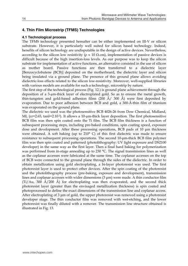
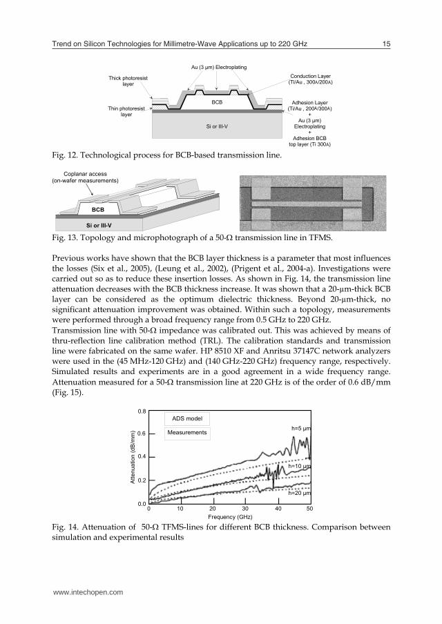
4. Thin Film Microstrip (TFMS) Technologies
4.1 Technological process The TFMS technology presented hereafter can be either implemented on III-V or silicon substrate. However, it is particularly well suited for silicon based technology. Indeed, benefits of silicon technology are undisputable in the design of active devices. Nevertheless, according to the silicon low resistivity ( 10 .cm), implementation of passive devices is difficult because of the high insertion-loss levels. As our purpose was to keep the silicon substrate for implementation of active functions, an alternative consisted in the use of silicon as mother board. Passive functions are then transferred to a dielectric layer [Benzocyclobutene (BCB)] deposited on the motherboard, the dielectric layer and silicon being insulated via a ground plane. The presence of this ground plane allows avoiding dielectric-loss effects related to the silicon low-resistivity. Moreover, well-supplied libraries with various models are available for such a technology, microstrip by nature. The first step of the technological process (Fig. 12.) is ground plane achievement through the deposition of a 3-µm-thick layer of electroplated gold. So as to ensure the metal growth, thin-tungsten and gold-based adhesion films (200 Å/ 300 Å) were first deposited by evaporation. Due to poor adhesion between BCB and gold, a 300-Å-thin film of titanium was evaporated on the ground plane. The dielectric we used was the photosensitive BCB 4026-26 from Dow Chemical, Midland, MI, (r=2.65, tan=2.10-3). It allows a 10-µm-thick layer deposition. The first photosensitive BCB film was then spin coated onto the Ti film. The BCB film thickness is a function of subsequent processing steps, including pre-baked conditions, spin coating speed, exposure dose and development. After these processing operations, BCB pads of 10 μm thickness were obtained. A soft baking (up to 210° C) of this first dielectric was made to ensure resistance to subsequent processing operations. The second 10-μm-thick BCB film polymer film was then spin coated and patterned (photolithography: UV light exposure and DS2100 developer) in the same way as the first layer. Then a final hard baking for polymerization was performed from in-stage annealing up to 230 °C. The signal transmission lines as well as the coplanar accesses were fabricated at the same time. The coplanar accesses on the top of BCB were connected to the ground plane through the sides of the dielectric. In order to obtain metallization using gold electroplating, a bi-layer photoresist was used. The first photoresist layer is used to protect other devices. After the spin coating of the photoresist and the photolithography process (pre-baking, exposure and development), transmission lines and coplanar accesses with wider dimensions (3 μm) were made. A thin conductor film (Ti/Au, 300 Å/200 Å) for electroplating was then evaporated, and the second thick photoresist layer (greater than the envisaged metallization thickness) is spin coated and photoprocessed to define the exact dimensions of the transmission line and coplanar access. After electroplating of 3 μm of gold, the upper photoresist was removed using a photoresist developer stage. The thin conductor film was removed with wet-etching, and the lower photoresist was finally diluted with a remover. The transmission line structure obtained is illustrated in Fig. 13.
Si or III-V
BCB
Thick photoresistlayer
Thin photoresistlayer
Au (3 µm) Electroplating
Adhesion Layer(Ti/Au , 200 /300 )
+Au (3 µm)
Electroplating+
Adhesion BCBtop layer (Ti 300 )
Conduction Layer(Ti/Au , 300 /200 )Å Å
Å Å
Å
Fig. 12. Technological process for BCB-based transmission line.
Coplanar access(on-wafer measurements)
Si or III-V
Si SubstrateBCBBCB
Fig. 13. Topology and microphotograph of a 50- transmission line in TFMS. Previous works have shown that the BCB layer thickness is a parameter that most influences the losses (Six et al., 2005), (Leung et al., 2002), (Prigent et al., 2004-a). Investigations were carried out so as to reduce these insertion losses. As shown in Fig. 14, the transmission line attenuation decreases with the BCB thickness increase. It was shown that a 20-µm-thick BCB layer can be considered as the optimum dielectric thickness. Beyond 20-µm-thick, no significant attenuation improvement was obtained. Within such a topology, measurements were performed through a broad frequency range from 0.5 GHz to 220 GHz. Transmission line with 50- impedance was calibrated out. This was achieved by means of thru-reflection line calibration method (TRL). The calibration standards and transmission line were fabricated on the same wafer. HP 8510 XF and Anritsu 37147C network analyzers were used in the (45 MHz-120 GHz) and (140 GHz-220 GHz) frequency range, respectively. Simulated results and experiments are in a good agreement in a wide frequency range. Attenuation measured for a 50- transmission line at 220 GHz is of the order of 0.6 dB/mm (Fig. 15).
Measurements
ADS model
Frequency (GHz)
0.4
0.2
0.00 10 20 30 40 50
0.6
0.8
Atte
nuat
ion
(dB
/mm
)
h=20 µm
h=10 µm
h=5 µm
Fig. 14. Attenuation of 50- TFMS-lines for different BCB thickness. Comparison between simulation and experimental results
www.intechopen.com
Trend on Silicon Technologies for Millimetre-Wave Applications up to 220 GHz 15
4. Thin Film Microstrip (TFMS) Technologies
4.1 Technological process The TFMS technology presented hereafter can be either implemented on III-V or silicon substrate. However, it is particularly well suited for silicon based technology. Indeed, benefits of silicon technology are undisputable in the design of active devices. Nevertheless, according to the silicon low resistivity ( 10 .cm), implementation of passive devices is difficult because of the high insertion-loss levels. As our purpose was to keep the silicon substrate for implementation of active functions, an alternative consisted in the use of silicon as mother board. Passive functions are then transferred to a dielectric layer [Benzocyclobutene (BCB)] deposited on the motherboard, the dielectric layer and silicon being insulated via a ground plane. The presence of this ground plane allows avoiding dielectric-loss effects related to the silicon low-resistivity. Moreover, well-supplied libraries with various models are available for such a technology, microstrip by nature. The first step of the technological process (Fig. 12.) is ground plane achievement through the deposition of a 3-µm-thick layer of electroplated gold. So as to ensure the metal growth, thin-tungsten and gold-based adhesion films (200 Å/ 300 Å) were first deposited by evaporation. Due to poor adhesion between BCB and gold, a 300-Å-thin film of titanium was evaporated on the ground plane. The dielectric we used was the photosensitive BCB 4026-26 from Dow Chemical, Midland, MI, (r=2.65, tan=2.10-3). It allows a 10-µm-thick layer deposition. The first photosensitive BCB film was then spin coated onto the Ti film. The BCB film thickness is a function of subsequent processing steps, including pre-baked conditions, spin coating speed, exposure dose and development. After these processing operations, BCB pads of 10 μm thickness were obtained. A soft baking (up to 210° C) of this first dielectric was made to ensure resistance to subsequent processing operations. The second 10-μm-thick BCB film polymer film was then spin coated and patterned (photolithography: UV light exposure and DS2100 developer) in the same way as the first layer. Then a final hard baking for polymerization was performed from in-stage annealing up to 230 °C. The signal transmission lines as well as the coplanar accesses were fabricated at the same time. The coplanar accesses on the top of BCB were connected to the ground plane through the sides of the dielectric. In order to obtain metallization using gold electroplating, a bi-layer photoresist was used. The first photoresist layer is used to protect other devices. After the spin coating of the photoresist and the photolithography process (pre-baking, exposure and development), transmission lines and coplanar accesses with wider dimensions (3 μm) were made. A thin conductor film (Ti/Au, 300 Å/200 Å) for electroplating was then evaporated, and the second thick photoresist layer (greater than the envisaged metallization thickness) is spin coated and photoprocessed to define the exact dimensions of the transmission line and coplanar access. After electroplating of 3 μm of gold, the upper photoresist was removed using a photoresist developer stage. The thin conductor film was removed with wet-etching, and the lower photoresist was finally diluted with a remover. The transmission line structure obtained is illustrated in Fig. 13.
Si or III-V
BCB
Thick photoresistlayer
Thin photoresistlayer
Au (3 µm) Electroplating
Adhesion Layer(Ti/Au , 200 /300 )
+Au (3 µm)
Electroplating+
Adhesion BCBtop layer (Ti 300 )
Conduction Layer(Ti/Au , 300 /200 )Å Å
Å Å
Å
Fig. 12. Technological process for BCB-based transmission line.
Coplanar access(on-wafer measurements)
Si or III-V
Si SubstrateBCBBCB
Fig. 13. Topology and microphotograph of a 50- transmission line in TFMS. Previous works have shown that the BCB layer thickness is a parameter that most influences the losses (Six et al., 2005), (Leung et al., 2002), (Prigent et al., 2004-a). Investigations were carried out so as to reduce these insertion losses. As shown in Fig. 14, the transmission line attenuation decreases with the BCB thickness increase. It was shown that a 20-µm-thick BCB layer can be considered as the optimum dielectric thickness. Beyond 20-µm-thick, no significant attenuation improvement was obtained. Within such a topology, measurements were performed through a broad frequency range from 0.5 GHz to 220 GHz. Transmission line with 50- impedance was calibrated out. This was achieved by means of thru-reflection line calibration method (TRL). The calibration standards and transmission line were fabricated on the same wafer. HP 8510 XF and Anritsu 37147C network analyzers were used in the (45 MHz-120 GHz) and (140 GHz-220 GHz) frequency range, respectively. Simulated results and experiments are in a good agreement in a wide frequency range. Attenuation measured for a 50- transmission line at 220 GHz is of the order of 0.6 dB/mm (Fig. 15).
Measurements
ADS model
Frequency (GHz)
0.4
0.2
0.00 10 20 30 40 50
0.6
0.8
Atte
nuat
ion
(dB
/mm
)
h=20 µm
h=10 µm
h=5 µm
Fig. 14. Attenuation of 50- TFMS-lines for different BCB thickness. Comparison between simulation and experimental results
www.intechopen.com
Microwave and Millimeter Wave Technologies: from Photonic Bandgap Devices to Antenna and Applications 16
Measurements
ADS model
Frequency (GHz)
Atte
nuat
ion
(dB
/mm
)
0.8
0.6
0.4
0.2
00 50 100 150 200 250
1.0
1.2
Effe
ctiv
e P
erm
itivi
ty ( r
eff)
Measurements
ADS model
Frequency (GHz)
2.4
2.2
2.00 50 100 150 200 250
2.6
2.8
Fig. 15. Comparison between simulation (ADS) and measurement results of a 50- TFMS-line with 20-µm BCB thickness up to 220 GHz.
4.2 Bandpass filter Design So as to illustrate the Si-BCB based thin film microstrip technology, the filter to be designed roughly corresponds to a U–band filter, the 3-dB passband is 49–51 GHz, the rejection level in the 41.15–46.15-GHz frequency band is 35 dB, and no specification for the upper band beyond 51 GHz is required. Coupled-line topologies are basically well suited for narrow bandpass filters. Nevertheless, in view of the desired insertion losses and rejection levels, such topologies become unsuitable with the above filter specifications. Indeed, the closeness of the passband and lower reject band imposes high rejection levels. Hence, the filter order has to be increased, which significantly degrades global insertion losses. These considerations have led us to choose a new filter topology based on dual behavior resonators (DBRs), which means both stopband and passband (Rizzi, 1988). Such a resonator results from two different open-ended stubs set in parallel. Each stub brings a transmission zero on either side of the passband. Development of a global synthesis enabled us to independently control the bandwidth, the upper and lower frequency bands, as well as the different transmission-zero frequencies of an nth-order filter, i.e., composed of DBRs (Quendo et al., 2003). Let us apply an alike development to the design of a 4th-order filter that meets the desired specifications. It results in a filter with four transmission zeros on both sides of the passband. These transmission zeros being independent, their frequencies are either separated or joined. This depends on the electrical length of the four resonators: they can differ or be identical (Fig. 16). For the sake of simplicity, the electrical characteristics of the upper frequency stubs, i.e., (L1a ,Z1a), (L2a, Z2a), (L3a, Z3a) and (L4a, Z4a), were chosen equal, which meant that the upper transmission zeros were joined. Similarly, the lower frequency stubs were of equal length, i.e., (L1b , L2b, L3b, and L4b), and the associated transmission zeros were joined. The filter was designed based on the joint use of the synthesis (Quendo et al., 2003) and the DOE based design method that allows simple and rapid correction process (Prigent et al., 2003-a), (Prigent et al., 2003-b), (Tagushi, 1987), (Prigent et al., 2002). As depicted in Fig. 17, the filter electrical response obtained with this design method was in a very good agreement with the simulations results (ADS-Momentum).
InZ01,L01 Z12,L12
Z1a,L1a
Z1b,L1b
Z23,L23
Z2a,L2a
Z2b,L2b
Z34,L34
Z3a,L3a
Z3b,L3b
Z45,L45
Z4a,L4a
Z4b,L4b
Out
0.0
-50.0
-30.0
-10.0
-20.0
-40.0
FREQUENCY (GHz) 65.0 40.0
0.0
-250.0
-150.0
-50.0
-100.0
-200.0
dB(S
11)
dB(S
21)
45.0 50.0 55.0 60.0
4 different DBRs4 Identical DBRs
Fig. 16. 4th-order ideal DBR topology and response : with different resonator type (impedance and length) or with four identical resonators.
Fig. 17. (a)Layout of the 4th-order DBR filter in U-band. (b) comparison of electromagnetic simulation with experiment, in wide frequency range up to 75 GHz (c).
4.3 Application in the G-band (140 GHz-220 GHz) According to the quality of the experimental results observed at 94 GHz, one has attempted to transpose our concepts to upper frequency domain in G-band (140-220 GHz). In this frequency range, the problems due to sensitivity and design accuracy are all the more important since the electrical lengths that are involved are very small. Let us consider the design of a 4th-oder classical shunt-stubs filter with 10% 3-dB-bandwidth. According to classical synthesis (Matthaei et al., 1980), while designing filter with such specifications, we are faced to technical impossibilities. Indeed, at this frequency level, transmission lines are wider than long. Hence, the electromagnetic simulation results are strongly debased. Moreover, the filter dimensions made the electrical response correction difficult, indeed impossible. So as to overcome such a difficulty, the solution we have developed (Prigent et al., 2005) consists in considering the first harmonic as the frequency of interest, not the fundamental frequency. Thus, the filter to be designed is a 4th-order filter with 60 GHz central frequency. In this way, one can reach the filter specifications while keeping a correct shape factor for the stubs (Fig. 18). Measurement results were made in 0-110 GHz and 140-220 GHz bands. Despite a slight insertion losses improvement, the measurement results are in a complete accordance with the desired specifications.
www.intechopen.com
Trend on Silicon Technologies for Millimetre-Wave Applications up to 220 GHz 17
Measurements
ADS model
Frequency (GHz)
Atte
nuat
ion
(dB
/mm
)
0.8
0.6
0.4
0.2
00 50 100 150 200 250
1.0
1.2
Effe
ctiv
e P
erm
itivi
ty ( r
eff)
Measurements
ADS model
Frequency (GHz)
2.4
2.2
2.00 50 100 150 200 250
2.6
2.8
Fig. 15. Comparison between simulation (ADS) and measurement results of a 50- TFMS-line with 20-µm BCB thickness up to 220 GHz.
4.2 Bandpass filter Design So as to illustrate the Si-BCB based thin film microstrip technology, the filter to be designed roughly corresponds to a U–band filter, the 3-dB passband is 49–51 GHz, the rejection level in the 41.15–46.15-GHz frequency band is 35 dB, and no specification for the upper band beyond 51 GHz is required. Coupled-line topologies are basically well suited for narrow bandpass filters. Nevertheless, in view of the desired insertion losses and rejection levels, such topologies become unsuitable with the above filter specifications. Indeed, the closeness of the passband and lower reject band imposes high rejection levels. Hence, the filter order has to be increased, which significantly degrades global insertion losses. These considerations have led us to choose a new filter topology based on dual behavior resonators (DBRs), which means both stopband and passband (Rizzi, 1988). Such a resonator results from two different open-ended stubs set in parallel. Each stub brings a transmission zero on either side of the passband. Development of a global synthesis enabled us to independently control the bandwidth, the upper and lower frequency bands, as well as the different transmission-zero frequencies of an nth-order filter, i.e., composed of DBRs (Quendo et al., 2003). Let us apply an alike development to the design of a 4th-order filter that meets the desired specifications. It results in a filter with four transmission zeros on both sides of the passband. These transmission zeros being independent, their frequencies are either separated or joined. This depends on the electrical length of the four resonators: they can differ or be identical (Fig. 16). For the sake of simplicity, the electrical characteristics of the upper frequency stubs, i.e., (L1a ,Z1a), (L2a, Z2a), (L3a, Z3a) and (L4a, Z4a), were chosen equal, which meant that the upper transmission zeros were joined. Similarly, the lower frequency stubs were of equal length, i.e., (L1b , L2b, L3b, and L4b), and the associated transmission zeros were joined. The filter was designed based on the joint use of the synthesis (Quendo et al., 2003) and the DOE based design method that allows simple and rapid correction process (Prigent et al., 2003-a), (Prigent et al., 2003-b), (Tagushi, 1987), (Prigent et al., 2002). As depicted in Fig. 17, the filter electrical response obtained with this design method was in a very good agreement with the simulations results (ADS-Momentum).
InZ01,L01 Z12,L12
Z1a,L1a
Z1b,L1b
Z23,L23
Z2a,L2a
Z2b,L2b
Z34,L34
Z3a,L3a
Z3b,L3b
Z45,L45
Z4a,L4a
Z4b,L4b
Out
0.0
-50.0
-30.0
-10.0
-20.0
-40.0
FREQUENCY (GHz) 65.0 40.0
0.0
-250.0
-150.0
-50.0
-100.0
-200.0
dB(S
11)
dB(S
21)
45.0 50.0 55.0 60.0
4 different DBRs4 Identical DBRs
Fig. 16. 4th-order ideal DBR topology and response : with different resonator type (impedance and length) or with four identical resonators.
Fig. 17. (a)Layout of the 4th-order DBR filter in U-band. (b) comparison of electromagnetic simulation with experiment, in wide frequency range up to 75 GHz (c).
4.3 Application in the G-band (140 GHz-220 GHz) According to the quality of the experimental results observed at 94 GHz, one has attempted to transpose our concepts to upper frequency domain in G-band (140-220 GHz). In this frequency range, the problems due to sensitivity and design accuracy are all the more important since the electrical lengths that are involved are very small. Let us consider the design of a 4th-oder classical shunt-stubs filter with 10% 3-dB-bandwidth. According to classical synthesis (Matthaei et al., 1980), while designing filter with such specifications, we are faced to technical impossibilities. Indeed, at this frequency level, transmission lines are wider than long. Hence, the electromagnetic simulation results are strongly debased. Moreover, the filter dimensions made the electrical response correction difficult, indeed impossible. So as to overcome such a difficulty, the solution we have developed (Prigent et al., 2005) consists in considering the first harmonic as the frequency of interest, not the fundamental frequency. Thus, the filter to be designed is a 4th-order filter with 60 GHz central frequency. In this way, one can reach the filter specifications while keeping a correct shape factor for the stubs (Fig. 18). Measurement results were made in 0-110 GHz and 140-220 GHz bands. Despite a slight insertion losses improvement, the measurement results are in a complete accordance with the desired specifications.
www.intechopen.com
Microwave and Millimeter Wave Technologies: from Photonic Bandgap Devices to Antenna and Applications 18
3143 µm
1773 µm
r=2.65h=20 µm
0 50 100 150 200 250
0
-50
-40
-30
-20
-10
dB(S
11)
dB(S
12)
FREQUENCY (GHz)EM Simulation Measurements Fig. 18. Electromagnetic simulation results (Momentum) of the 4th-order shunt-stub filter with 60 GHz central frequency. Comparison with experimental results in 0-220 GHz band. Within these conditions, there still remains the fundamental frequency which could be harmful in a global system insertion perspective. As a consequence, the fundamental harmonic has to be suppressed using insertion of filtering functions, such as high- or band-pass filters, in the nominal band-pass device. Considering the filter electrical response (Fig. 18) the solution we advocated is the insertion of high-pass filter. The filter to be designed is a 2nd-order high-pass filter with 130 GHz cutoff frequency. The BCB technology contributes to realize the series capacitance which is usually difficult to achieve in 2D planar technologies. Indeed, it was possible to take advantage of the Si-BCB topology to realize multi-layer capacitance. It consists of a CPW to TFMS transition based upon the use of capacitive coupling between the main conductor of the TFMS-line and the coplanar guide, through the thin dielectric layer. The final high-pass filter topology is described in Fig. 19.
Level 1CPW
+
BCB20 µm
+
Level 2TFMS strip
=
0 50 100 150 200 250
0
-50
-40
-30
-20
-10
dB(S
11)
dB(S
12)
FREQUENCY (GHz) Fig. 19. Layout and simulation results (Ansoft - HFSS) of the 2nd-order high-pass filter with 130 GHz central frequency. Comparison with the bandpass filter electrical response. One just has to insert this high-pass cells at the in/out access lines level. The electromagnetic simulation results of the resulting band-pass filter topology (Fig. 20) attest from this design method contribution toward the design of band-pass filter in very high frequency range. Indeed, the fundamental harmonic was suppressed while keeping the filter bandwidth as well as correct return losses.
High-pass High-passBand-pass
Metal growth on the BCB side :Short-ended
0 50 100 150 200 250
0
-50
-40
-30
-20
-10
dB(S
11)
dB(S
12)
FREQUENCY (GHz) Fig. 20. Layout and electromagnetic simulation results (HFSS) of the final bandpass filter at 180 GHz with 10% 3-dB-bandwidth. Comparison with the initial bandpass filter response. According to the previous results, one has attempted to apply the design method for a narrower band-pass filter. The filter to be designed is a 3rd-order DBR filter at 180 GHz with 5% 3-dB-bandwidth. If the design of previous filter was limited to reduction of the first harmonic, it is not the same for DBR filters. Indeed, by order of the resonators nature, the electrical response of DBR filters presents spurious resonances on either side of the pass-band. Moreover, as the filter was designed with 60 GHz central frequency, the frequency of interest being 180 GHz, spurious response level is very important compared with the filter bandwidth (Fig. 21). Therefore, sizeable modifications had to be brought to the filter design. The first step of the design consisted in spurious resonance attenuation. This was achieved using integration of the DBR filter in the previous shunt-stub band-pass-filter. In this way, as the shunt-stub filter bandwidth is twice the DBR ones, both fundamental and first harmonics of the DBR filter were preserved while taking advantage of the shunt-stub filter rejection level for out-of-band improvement (Fig. 22). Finally, it only remained to suppress the fundamental frequency using the high-pass filter previously designed (Fig. 23).
0 20 60 100 180 220
0
-50
-40
-30
-20
-10
dB(S
11)
dB(S
12)
FREQUENCY (GHz)140
0
-100
-80
-60
-40
-20
EM Simulation Measurements Fig. 21. Layout and simulation results (Momentum) of a 3rd-order DBR filter at 180 GHz with 5% 3-dB-bandwidth. Comparison with experimental results in 0-220 GHz band.
www.intechopen.com
Trend on Silicon Technologies for Millimetre-Wave Applications up to 220 GHz 19
3143 µm
1773 µm
r=2.65h=20 µm
0 50 100 150 200 250
0
-50
-40
-30
-20
-10
dB(S
11)
dB(S
12)
FREQUENCY (GHz)EM Simulation Measurements Fig. 18. Electromagnetic simulation results (Momentum) of the 4th-order shunt-stub filter with 60 GHz central frequency. Comparison with experimental results in 0-220 GHz band. Within these conditions, there still remains the fundamental frequency which could be harmful in a global system insertion perspective. As a consequence, the fundamental harmonic has to be suppressed using insertion of filtering functions, such as high- or band-pass filters, in the nominal band-pass device. Considering the filter electrical response (Fig. 18) the solution we advocated is the insertion of high-pass filter. The filter to be designed is a 2nd-order high-pass filter with 130 GHz cutoff frequency. The BCB technology contributes to realize the series capacitance which is usually difficult to achieve in 2D planar technologies. Indeed, it was possible to take advantage of the Si-BCB topology to realize multi-layer capacitance. It consists of a CPW to TFMS transition based upon the use of capacitive coupling between the main conductor of the TFMS-line and the coplanar guide, through the thin dielectric layer. The final high-pass filter topology is described in Fig. 19.
Level 1CPW
+
BCB20 µm
+
Level 2TFMS strip
=
0 50 100 150 200 250
0
-50
-40
-30
-20
-10
dB(S
11)
dB(S
12)
FREQUENCY (GHz) Fig. 19. Layout and simulation results (Ansoft - HFSS) of the 2nd-order high-pass filter with 130 GHz central frequency. Comparison with the bandpass filter electrical response. One just has to insert this high-pass cells at the in/out access lines level. The electromagnetic simulation results of the resulting band-pass filter topology (Fig. 20) attest from this design method contribution toward the design of band-pass filter in very high frequency range. Indeed, the fundamental harmonic was suppressed while keeping the filter bandwidth as well as correct return losses.
High-pass High-passBand-pass
Metal growth on the BCB side :Short-ended
0 50 100 150 200 250
0
-50
-40
-30
-20
-10
dB(S
11)
dB(S
12)
FREQUENCY (GHz) Fig. 20. Layout and electromagnetic simulation results (HFSS) of the final bandpass filter at 180 GHz with 10% 3-dB-bandwidth. Comparison with the initial bandpass filter response. According to the previous results, one has attempted to apply the design method for a narrower band-pass filter. The filter to be designed is a 3rd-order DBR filter at 180 GHz with 5% 3-dB-bandwidth. If the design of previous filter was limited to reduction of the first harmonic, it is not the same for DBR filters. Indeed, by order of the resonators nature, the electrical response of DBR filters presents spurious resonances on either side of the pass-band. Moreover, as the filter was designed with 60 GHz central frequency, the frequency of interest being 180 GHz, spurious response level is very important compared with the filter bandwidth (Fig. 21). Therefore, sizeable modifications had to be brought to the filter design. The first step of the design consisted in spurious resonance attenuation. This was achieved using integration of the DBR filter in the previous shunt-stub band-pass-filter. In this way, as the shunt-stub filter bandwidth is twice the DBR ones, both fundamental and first harmonics of the DBR filter were preserved while taking advantage of the shunt-stub filter rejection level for out-of-band improvement (Fig. 22). Finally, it only remained to suppress the fundamental frequency using the high-pass filter previously designed (Fig. 23).
0 20 60 100 180 220
0
-50
-40
-30
-20
-10
dB(S
11)
dB(S
12)
FREQUENCY (GHz)140
0
-100
-80
-60
-40
-20
EM Simulation Measurements Fig. 21. Layout and simulation results (Momentum) of a 3rd-order DBR filter at 180 GHz with 5% 3-dB-bandwidth. Comparison with experimental results in 0-220 GHz band.
www.intechopen.com
Microwave and Millimeter Wave Technologies: from Photonic Bandgap Devices to Antenna and Applications 20
DBR Filtershunt-stub filter
shunt-stub filter
0 20 60 100 180 220
0
-50
-40
-30
-20
-10
dB(S
11)
dB(S
12)
FREQUENCY (GHz)140
0
-100
-80
-60
-40
-20
EM Simulation Measurements Fig. 22. Layout and electromagnetic simulation results of DBR filter integration in classical shunt-stub filter. Comparison with experimental results in 0-220 GHz frequency band.
DBR Filter + High-pass
filterHigh-pass
filterShunt-stub
filter0 20 60 100 180 220
0
-50
-40
-30
-20
-10dB
(S11
)
dB(S
12)
FREQUENCY (GHz)140
0
-100
-80
-60
-40
-20
Fig. 23. Layout and electromagnetic simulation results of the final bandpass filter at 180 GHz with 5% 3-dB-bandwidth. Comparison with the initial DBR filter response. Comparison made between theoretical and measurement results over a wide frequency range up to 220 GHz evidenced the efficiency of the design method we developed as well as the accuracy of BCB technology for the design of passive function for very high frequencies. These concepts were demonstrated, not only for filters, but also for other passive functions such as couplers or balanced matching networks (Prigent et al., 2006a), (Prigent et al., 2006b).
5. Advanced CMOS SOI technology on High Resistivity substrate
5.1 65 nm MOSFET Performances Through careful optimization and modelling rules for active and passive components, a standard 0.13 µm CMOS process was proved to be capable of 60 GHz operation despite the related low Ft/Fmax which was in the order of 100 GHz (Doan et al., 2004). Measurements of 65-nm CMOS technology (Dambrine et al., 2005) demonstrate Ft of 220 GHz and Fmax of 240 GHz (Fig. 24), which are clearly comparable to advanced commercially available 100 nm III-V HEMT or state-of-the-art SiGe HBT (Chevalier et al., 2004). Moreover, HF noise figure is in the order of 2 dB at 40 GHz. As a consequence, from active devices point of view there is no reason to prevent the integration of millimetre-wave applications in CMOS technology.
Fig. 24. Measured gains for 64x1/0.06 NMOS in 65nm bulk technology (IDS/W=439 µA/µm, VDS=1.2V). NFmin and Gass vs frequency for 50x2x0.055 µm2 n-MOSFET (VDS=0.7 V, IDS=100 mA/mm).
5.2 65nm On-Chip Transmission line performances up to 220 GHz The integration of high quality passive components in standard silicon technology is not obvious. It is well known that passive components integrated in standard silicon technologies suffer from high substrate losses. This point is clearly the fundamental limitation for conventional bulk technologies (either CMOS or BiCMOS) to address millimetre-wave applications. But recently (Gianesello et al., 2006-a), high quality passive components (Coplanar Waveguide with less than 1 dB/mm of losses @ 100 GHz) integrated in advanced 130 nm HR SOI CMOS technology have demonstrated performances comparable to state of the art III-V technologies up to W band (75-100 GHz). At millimetre-wave frequency range, the use of transmission lines is generally preferred to integrate passive components since implementation of spiral inductors is feasible but suffers from accuracy issues. Two kinds of structures can be considered, transmission lines which are sensitive to substrate effects (CPW presented in Fig. 25) and transmission lines which do not (microstrip with ground plane as shield not presented here). Since microstrip transmission lines have demonstrated electrical performances worse than CPW ones in advanced standard digital silicon Back-End-Of-Line (BEOL) with HR substrate (Gianesello, et al., 2007) we have focused our attention on coplanar transmission lines achieved on HR SOI.
Fig. 25. Coplanar transmission line structure. Since it has been demonstrated that in HR SOI substrate losses are drastically reduced, we propose here the use of a new stacked coplanar transmission line dedicated to HR SOI technology. By doing so, we can reduce the metallic losses which occur in the transmission line. Moreover, this kind of coplanar transmission line is very similar to the one integrated
www.intechopen.com
Trend on Silicon Technologies for Millimetre-Wave Applications up to 220 GHz 21
DBR Filtershunt-stub filter
shunt-stub filter
0 20 60 100 180 220
0
-50
-40
-30
-20
-10
dB(S
11)
dB(S
12)
FREQUENCY (GHz)140
0
-100
-80
-60
-40
-20
EM Simulation Measurements Fig. 22. Layout and electromagnetic simulation results of DBR filter integration in classical shunt-stub filter. Comparison with experimental results in 0-220 GHz frequency band.
DBR Filter + High-pass
filterHigh-pass
filterShunt-stub
filter0 20 60 100 180 220
0
-50
-40
-30
-20
-10
dB(S
11)
dB(S
12)
FREQUENCY (GHz)140
0
-100
-80
-60
-40
-20
Fig. 23. Layout and electromagnetic simulation results of the final bandpass filter at 180 GHz with 5% 3-dB-bandwidth. Comparison with the initial DBR filter response. Comparison made between theoretical and measurement results over a wide frequency range up to 220 GHz evidenced the efficiency of the design method we developed as well as the accuracy of BCB technology for the design of passive function for very high frequencies. These concepts were demonstrated, not only for filters, but also for other passive functions such as couplers or balanced matching networks (Prigent et al., 2006a), (Prigent et al., 2006b).
5. Advanced CMOS SOI technology on High Resistivity substrate
5.1 65 nm MOSFET Performances Through careful optimization and modelling rules for active and passive components, a standard 0.13 µm CMOS process was proved to be capable of 60 GHz operation despite the related low Ft/Fmax which was in the order of 100 GHz (Doan et al., 2004). Measurements of 65-nm CMOS technology (Dambrine et al., 2005) demonstrate Ft of 220 GHz and Fmax of 240 GHz (Fig. 24), which are clearly comparable to advanced commercially available 100 nm III-V HEMT or state-of-the-art SiGe HBT (Chevalier et al., 2004). Moreover, HF noise figure is in the order of 2 dB at 40 GHz. As a consequence, from active devices point of view there is no reason to prevent the integration of millimetre-wave applications in CMOS technology.
Fig. 24. Measured gains for 64x1/0.06 NMOS in 65nm bulk technology (IDS/W=439 µA/µm, VDS=1.2V). NFmin and Gass vs frequency for 50x2x0.055 µm2 n-MOSFET (VDS=0.7 V, IDS=100 mA/mm).
5.2 65nm On-Chip Transmission line performances up to 220 GHz The integration of high quality passive components in standard silicon technology is not obvious. It is well known that passive components integrated in standard silicon technologies suffer from high substrate losses. This point is clearly the fundamental limitation for conventional bulk technologies (either CMOS or BiCMOS) to address millimetre-wave applications. But recently (Gianesello et al., 2006-a), high quality passive components (Coplanar Waveguide with less than 1 dB/mm of losses @ 100 GHz) integrated in advanced 130 nm HR SOI CMOS technology have demonstrated performances comparable to state of the art III-V technologies up to W band (75-100 GHz). At millimetre-wave frequency range, the use of transmission lines is generally preferred to integrate passive components since implementation of spiral inductors is feasible but suffers from accuracy issues. Two kinds of structures can be considered, transmission lines which are sensitive to substrate effects (CPW presented in Fig. 25) and transmission lines which do not (microstrip with ground plane as shield not presented here). Since microstrip transmission lines have demonstrated electrical performances worse than CPW ones in advanced standard digital silicon Back-End-Of-Line (BEOL) with HR substrate (Gianesello, et al., 2007) we have focused our attention on coplanar transmission lines achieved on HR SOI.
Fig. 25. Coplanar transmission line structure. Since it has been demonstrated that in HR SOI substrate losses are drastically reduced, we propose here the use of a new stacked coplanar transmission line dedicated to HR SOI technology. By doing so, we can reduce the metallic losses which occur in the transmission line. Moreover, this kind of coplanar transmission line is very similar to the one integrated
www.intechopen.com
Microwave and Millimeter Wave Technologies: from Photonic Bandgap Devices to Antenna and Applications 22
in III-V since it lies directly on the silicon substrate. Hence, one can use similar dimension rules than in III-V. For example, in this work a ground-to-ground dimension of 35µm was used which is the typical dimension used in III-V at G-band. On chip transmission lines reported in this work were fabricated in advanced SOI CMOS technology with Cu damascene back-end-of-line (BEOL). The BEOL layers configuration depicted in Fig. 26 is composed of six levels of copper: M1-M5 Layers are 0.35µm-thick whereas M6 is 0.9µm-thick. Additional aluminium layer is deposited as top level. Each coppers level are separated by 0.4µm-thick dielectric layer (SiO2) and connected with via-holes. On-wafer measurements have been performed up to 110 GHz using an Agilent HP8510XF Vector Network Analyzer, and from 140 to 220 GHz using Anritsu 37147C VNA and Oleson test heads. Phase velocity of this stacked CPW transmission line is fully linear up to 220 GHz (Fig. 26) which ensures a quasi-TEM propagation mode. State-of-the-art attenuation, in the order of 1 dB/mm @ 100GHz and 1.5 dB/mm @200 GHz, has been measured (Gianesello, Gloria et al., 2007).
Fig. 26. Stacked Coplanar transmission line architecture dedicated to HR SOI technologies. Measured phase velocity and attenuation of a 50 stacked coplanar transmission line (Ws=11 µm, g=12 µm, WM=105 µm).
5.3 Bandpass filter application To illustrate the performance of the CPW Transmission lines realized in HR SOI technologies, a CPW stub-based filter has been realized on bulk (65nm and 130 nm) and HR SOI substrate. Photography of the filter is depicted in Fig. 27. The filter was designed to have its fundamental response between 60 and 80 GHz. This filter was measured up to 220 GHz (Fig. 27) to investigate CPW transmission line performance at millimetre-wave range. The insertion loss of the filter realized in 65 nm is close to that of the same filter realized in 130 nm bulk (but shows 1 dB higher loss). This is due to the fact that we have to work closer from the substrate in 65-nm bulk technology because of BEOL structure and so substrate losses are more important. Beyond 100 GHz, no bulk filter is workable because of the bad performance achieved with bulk CPW at this frequency range. On the contrary, the filter implemented in HR SOI technology is fully workable up to 200 GHz. It demonstrates 6 dB less losses in the 60-80 GHz band, and even at 200 GHz it has only around 4.5 dB losses, which is better than the performance achieved by bulk filters at 80 GHz. The electrical performances were compared with equivalent topology developed in GaAs technology (Fig. 5) (Rius et al., 2003), (Wolf et al., 2005). Table 1 evidences that performances
M6M5M4M3M2M1
HR Substrate
AluCap
SiO2
5µm
were comparable to state of art III-V technologies. Indeed, even if central frequencies were not identical, but of the same order (70-GHz for HR SOI, 82-GHz for GaAs), the relative bandwidth being identical, the filter developed in HR SOI technology exhibits an insertion losses level of 2.01 dB which is very close to the one obtained in GaAs technology (1.8 dB).
Fig. 27. Simulated and measured results for classical 3rd-order shunt stub bandpass filter. Electrical performances comparisons for filters implemented in different technologies.
65nm Bulk
130nm Bulk HR SOI GaAs
dB(S21) @ f=f0 9.1 7.9 2.01 1.8
Table 1. Comparison of the 3rd-order CPW filter performances for 3rd-order bandpass filter One should note that the proposed technology (HR-SOI) provides solutions towards coplanar transmission lines. Indeed, generally odd-mode filters are realized with air-bridges which suffer from mechanical stability. In the present technological process, as the metallization consists of 7 metal layers, all layers being stacked on HR-SOI so as to reduce metallic losses, the bridge realization lies in three steps: Transmission lines and bridge definition on the first layer, transmission line aperture in layers 2-6, transmission line definition in top level metal (Fig. 28).
Bottom Layer 2nd-5th Layers Top Layer Fig. 28. Metal layers definition for bridge realization. For narrowbandpass filter, the filter that we have developed has a topology with direct tapped-line access. The choice of this topology was dictated by problems of realization and minimizing losses (Prigent et al., 2003). Indeed, according to the filter synthesis, a degree of freedom is available that allows to modify the even- and odd-modes impedances of
130 nm bulk
65 nm bulk
Electrical simulation with TL developed model in HR SOI
HR SOI
www.intechopen.com
Trend on Silicon Technologies for Millimetre-Wave Applications up to 220 GHz 23
in III-V since it lies directly on the silicon substrate. Hence, one can use similar dimension rules than in III-V. For example, in this work a ground-to-ground dimension of 35µm was used which is the typical dimension used in III-V at G-band. On chip transmission lines reported in this work were fabricated in advanced SOI CMOS technology with Cu damascene back-end-of-line (BEOL). The BEOL layers configuration depicted in Fig. 26 is composed of six levels of copper: M1-M5 Layers are 0.35µm-thick whereas M6 is 0.9µm-thick. Additional aluminium layer is deposited as top level. Each coppers level are separated by 0.4µm-thick dielectric layer (SiO2) and connected with via-holes. On-wafer measurements have been performed up to 110 GHz using an Agilent HP8510XF Vector Network Analyzer, and from 140 to 220 GHz using Anritsu 37147C VNA and Oleson test heads. Phase velocity of this stacked CPW transmission line is fully linear up to 220 GHz (Fig. 26) which ensures a quasi-TEM propagation mode. State-of-the-art attenuation, in the order of 1 dB/mm @ 100GHz and 1.5 dB/mm @200 GHz, has been measured (Gianesello, Gloria et al., 2007).
Fig. 26. Stacked Coplanar transmission line architecture dedicated to HR SOI technologies. Measured phase velocity and attenuation of a 50 stacked coplanar transmission line (Ws=11 µm, g=12 µm, WM=105 µm).
5.3 Bandpass filter application To illustrate the performance of the CPW Transmission lines realized in HR SOI technologies, a CPW stub-based filter has been realized on bulk (65nm and 130 nm) and HR SOI substrate. Photography of the filter is depicted in Fig. 27. The filter was designed to have its fundamental response between 60 and 80 GHz. This filter was measured up to 220 GHz (Fig. 27) to investigate CPW transmission line performance at millimetre-wave range. The insertion loss of the filter realized in 65 nm is close to that of the same filter realized in 130 nm bulk (but shows 1 dB higher loss). This is due to the fact that we have to work closer from the substrate in 65-nm bulk technology because of BEOL structure and so substrate losses are more important. Beyond 100 GHz, no bulk filter is workable because of the bad performance achieved with bulk CPW at this frequency range. On the contrary, the filter implemented in HR SOI technology is fully workable up to 200 GHz. It demonstrates 6 dB less losses in the 60-80 GHz band, and even at 200 GHz it has only around 4.5 dB losses, which is better than the performance achieved by bulk filters at 80 GHz. The electrical performances were compared with equivalent topology developed in GaAs technology (Fig. 5) (Rius et al., 2003), (Wolf et al., 2005). Table 1 evidences that performances
M6M5M4M3M2M1
HR Substrate
AluCap
SiO2
5µm
were comparable to state of art III-V technologies. Indeed, even if central frequencies were not identical, but of the same order (70-GHz for HR SOI, 82-GHz for GaAs), the relative bandwidth being identical, the filter developed in HR SOI technology exhibits an insertion losses level of 2.01 dB which is very close to the one obtained in GaAs technology (1.8 dB).
Fig. 27. Simulated and measured results for classical 3rd-order shunt stub bandpass filter. Electrical performances comparisons for filters implemented in different technologies.
65nm Bulk
130nm Bulk HR SOI GaAs
dB(S21) @ f=f0 9.1 7.9 2.01 1.8
Table 1. Comparison of the 3rd-order CPW filter performances for 3rd-order bandpass filter One should note that the proposed technology (HR-SOI) provides solutions towards coplanar transmission lines. Indeed, generally odd-mode filters are realized with air-bridges which suffer from mechanical stability. In the present technological process, as the metallization consists of 7 metal layers, all layers being stacked on HR-SOI so as to reduce metallic losses, the bridge realization lies in three steps: Transmission lines and bridge definition on the first layer, transmission line aperture in layers 2-6, transmission line definition in top level metal (Fig. 28).
Bottom Layer 2nd-5th Layers Top Layer Fig. 28. Metal layers definition for bridge realization. For narrowbandpass filter, the filter that we have developed has a topology with direct tapped-line access. The choice of this topology was dictated by problems of realization and minimizing losses (Prigent et al., 2003). Indeed, according to the filter synthesis, a degree of freedom is available that allows to modify the even- and odd-modes impedances of
130 nm bulk
65 nm bulk
Electrical simulation with TL developed model in HR SOI
HR SOI
www.intechopen.com
Microwave and Millimeter Wave Technologies: from Photonic Bandgap Devices to Antenna and Applications 24
constitutive coupled-lines. Thus, the transmission lines quality factor can be improved. Nevertheless, this parameter has a poor influence on the input/output coupled lines, which significantly limits the insertion losses improvement. Moreover, these coupled lines are very difficult to achieve in considering the technological constraints. Finally, the input/output lines do not participate in the definition of the filter order but adjust the level of return loss. Thus, a very convenient way to overcome this limitation consists in replacing the in/out coupled lines by tapped-line feedings as depicted in Fig. 29 (Dishal, 1965), (Cristal, 1975 ), (Cohn, 1974) which allows for a reduction in size as well as an extra transmission zero.
Zoe01
In
Out
Zoo01 Zoe12
Zoo12 Zoe23
Zoo23 Zoe34
Zoo34
g/4
g/4
g/4
g/4
In
50
Zoe12
Zoo12 Zoe23
Zoo23
g/4
g/4
g/4
e i
50
50
g/4
ei
50
Out FREQUENCY (GHz)
0.0
-50.0
-20.0
-30.0
-40.0
8040
dB(S
11)
dB(S
12)
6050 70
ClassicalFilter
ModifiedFilter
-10.0
Fig. 29. Comparison between response of classical and modified 3rd-order coupled-lines filter. The modified filter topology was designed in coplanar technology implemented in HR SOI CMOS. Measurement results depicted in Fig. 30 show a frequency shift of the order of 5%, as well as return loss degradation. Nevertheless, with regard to the filter geometry complexity, those results are encouraging since insertion loss obtained are 6.6 dB in spite of the poor matching level, it should be enhanced while improving the return loss. For instance, equivalent bandpass filter implemented on massive silicon substrate would have led to more than 10-dB insertion losses.
FREQUENCY (GHz)
0.0
-80.0
-20.0
-40.0
-60.0
1200
F2
F2= 63.25 GHzS21= -6.642 dB
dB(S
11)
dB(S
12)
20 40 60 80 100
F1
MEASUREMENT
F1= 60.00 GHzS21= -5.72 dB
SIMULATION
Fig. 30. Bottom metal layer, photography and measurement results of the 3rd-order bandpass filter @ 60 GHz.
2228 µm
819 µm
6. Conclusion
The design of bandpass filters were investigated, using III-V, Silicon Membrane Technology, TFMS technology on Si-BCB and CMOS HR-SOI. If advantages of III-V technologies are undisputable toward electrical performances for passive function, silicon technologies are becoming more competitive and achieve the performance level of the state of the art of III-V. Up to now, the exploitation of V, W and G bands has been minimal because of the high cost of III-V technology needed to process the millimetre-wave signals. Use of advanced HR SOI CMOS technology, according to 65 nm MOSFET performances and HR SOI filters presented in this chapter, makes now feasible the offer of CMOS low cost MMW mass market applications up to G band. Thus, HR SOI seems to be a good candidate in the coming year to address both low cost and low power mass market CMOS digital and RF/ MMW applications. Moreover, as HR SOI benchmark is multilayer by nature, implementation of filters in multilevel technologies could afford interesting properties.
7. References
Aftanasar, M. S.; Young, P. R.; Robertson, I. D.; Minalgiene, J. & Lucyszyn, S. (2001). Photoimageable thick-film millimeter-wave metal-pipe rectangular waveguides, Electronic Letters, vol 37, no 18, pp 1122-1123, August 2001, ISSN : 0013-5194.
Argarwal, B.; Schmitz, A. E.; Brown, J. J.; Matloubian, M.; Case, M. G.; Le, M.; Lui, M. & Rodwell, M. J. W. (1998). 112-GHz, 157-GHz, and 180-GHz InP HEMT traveling-wave amplifiers, IEEE Transactions on Microwave Theory and Techniques, vol. 46, no 12, pp 2553-2559, December 2005, ISSN : 0018-9480
Beilenhoff, K.; Heinrich, W. & Hartnagel, H. L. (1991). The scattering behaviour of air bridges in coplanar MMICs, Proceedings of European Microwave Conference, Roma, Italy, October 1976, vol. 2, pp. 1131–1135. Artech House, Boston London, UK.
Brauchler, F.; Robertson, S.; East, J. & Katehi, L. P. B. (1996). W band FGC line circuit elements, Proceedings of IEEE Microwave Theory and Techniques International Symposium, San Francisco, CA, 1996, pp 1845–1848, ISBN : 0-7803-3246-6, San Francisco CA, USA, June 1996, IEEE, Picataway NJ, USA.
Chevalier P.; Fellous C.; Rubaldo L.; Dutartre D.; Laurens M.; Jagueneau T.; Leverd F.; Bord S.; Richard C.; Lenoble D. ; Bonnouvrier J.; Marty M.; Perrotin A.; Gloria D.; Saguin F.; Barbalat B.; Beerkens R.; Zerounian N.; ANniel F. & Chantre A. (2004). 230 GHz self-aligned SiGeC HBT for 90 nm BiCMOS technology, Proceeding of the IEEE Bipolar/BiCMOS Circuits and Technology Meetings, pp 225–228, ISBN : 0-7803-8618-3, Montreal PQ, Canada, September 2004, IEEE, Picataway NJ, USA.Cohn, S. B. (1959). Dissipation loss in multiple-coupled-resonator filters, Proceedings of IRE, vol. 47, no 8, pp 1342–1348,August 1959, ISSN : 0096-8390.
Cohn, S. B. (1974). Generalized design of bandpass and other filters by computer optimization, Proceedings of IEEE Transactions on Microwave Theory and Techniques Internanional Symposium, Atlanta, USA, 1974, pp 272–274, ISBN : 0-7803-3246-6, Atlanta, USA, December 1974, IEEE, Picataway NJ, USA.
www.intechopen.com
Trend on Silicon Technologies for Millimetre-Wave Applications up to 220 GHz 25
constitutive coupled-lines. Thus, the transmission lines quality factor can be improved. Nevertheless, this parameter has a poor influence on the input/output coupled lines, which significantly limits the insertion losses improvement. Moreover, these coupled lines are very difficult to achieve in considering the technological constraints. Finally, the input/output lines do not participate in the definition of the filter order but adjust the level of return loss. Thus, a very convenient way to overcome this limitation consists in replacing the in/out coupled lines by tapped-line feedings as depicted in Fig. 29 (Dishal, 1965), (Cristal, 1975 ), (Cohn, 1974) which allows for a reduction in size as well as an extra transmission zero.
Zoe01
In
Out
Zoo01 Zoe12
Zoo12 Zoe23
Zoo23 Zoe34
Zoo34
g/4
g/4
g/4
g/4
In
50
Zoe12
Zoo12 Zoe23
Zoo23
g/4
g/4
g/4
e i
50
50
g/4
ei
50
Out FREQUENCY (GHz)
0.0
-50.0
-20.0
-30.0
-40.0
8040
dB(S
11)
dB(S
12)
6050 70
ClassicalFilter
ModifiedFilter
-10.0
Fig. 29. Comparison between response of classical and modified 3rd-order coupled-lines filter. The modified filter topology was designed in coplanar technology implemented in HR SOI CMOS. Measurement results depicted in Fig. 30 show a frequency shift of the order of 5%, as well as return loss degradation. Nevertheless, with regard to the filter geometry complexity, those results are encouraging since insertion loss obtained are 6.6 dB in spite of the poor matching level, it should be enhanced while improving the return loss. For instance, equivalent bandpass filter implemented on massive silicon substrate would have led to more than 10-dB insertion losses.
FREQUENCY (GHz)
0.0
-80.0
-20.0
-40.0
-60.0
1200
F2
F2= 63.25 GHzS21= -6.642 dB
dB(S
11)
dB(S
12)
20 40 60 80 100
F1
MEASUREMENT
F1= 60.00 GHzS21= -5.72 dB
SIMULATION
Fig. 30. Bottom metal layer, photography and measurement results of the 3rd-order bandpass filter @ 60 GHz.
2228 µm
819 µm
6. Conclusion
The design of bandpass filters were investigated, using III-V, Silicon Membrane Technology, TFMS technology on Si-BCB and CMOS HR-SOI. If advantages of III-V technologies are undisputable toward electrical performances for passive function, silicon technologies are becoming more competitive and achieve the performance level of the state of the art of III-V. Up to now, the exploitation of V, W and G bands has been minimal because of the high cost of III-V technology needed to process the millimetre-wave signals. Use of advanced HR SOI CMOS technology, according to 65 nm MOSFET performances and HR SOI filters presented in this chapter, makes now feasible the offer of CMOS low cost MMW mass market applications up to G band. Thus, HR SOI seems to be a good candidate in the coming year to address both low cost and low power mass market CMOS digital and RF/ MMW applications. Moreover, as HR SOI benchmark is multilayer by nature, implementation of filters in multilevel technologies could afford interesting properties.
7. References
Aftanasar, M. S.; Young, P. R.; Robertson, I. D.; Minalgiene, J. & Lucyszyn, S. (2001). Photoimageable thick-film millimeter-wave metal-pipe rectangular waveguides, Electronic Letters, vol 37, no 18, pp 1122-1123, August 2001, ISSN : 0013-5194.
Argarwal, B.; Schmitz, A. E.; Brown, J. J.; Matloubian, M.; Case, M. G.; Le, M.; Lui, M. & Rodwell, M. J. W. (1998). 112-GHz, 157-GHz, and 180-GHz InP HEMT traveling-wave amplifiers, IEEE Transactions on Microwave Theory and Techniques, vol. 46, no 12, pp 2553-2559, December 2005, ISSN : 0018-9480
Beilenhoff, K.; Heinrich, W. & Hartnagel, H. L. (1991). The scattering behaviour of air bridges in coplanar MMICs, Proceedings of European Microwave Conference, Roma, Italy, October 1976, vol. 2, pp. 1131–1135. Artech House, Boston London, UK.
Brauchler, F.; Robertson, S.; East, J. & Katehi, L. P. B. (1996). W band FGC line circuit elements, Proceedings of IEEE Microwave Theory and Techniques International Symposium, San Francisco, CA, 1996, pp 1845–1848, ISBN : 0-7803-3246-6, San Francisco CA, USA, June 1996, IEEE, Picataway NJ, USA.
Chevalier P.; Fellous C.; Rubaldo L.; Dutartre D.; Laurens M.; Jagueneau T.; Leverd F.; Bord S.; Richard C.; Lenoble D. ; Bonnouvrier J.; Marty M.; Perrotin A.; Gloria D.; Saguin F.; Barbalat B.; Beerkens R.; Zerounian N.; ANniel F. & Chantre A. (2004). 230 GHz self-aligned SiGeC HBT for 90 nm BiCMOS technology, Proceeding of the IEEE Bipolar/BiCMOS Circuits and Technology Meetings, pp 225–228, ISBN : 0-7803-8618-3, Montreal PQ, Canada, September 2004, IEEE, Picataway NJ, USA.Cohn, S. B. (1959). Dissipation loss in multiple-coupled-resonator filters, Proceedings of IRE, vol. 47, no 8, pp 1342–1348,August 1959, ISSN : 0096-8390.
Cohn, S. B. (1974). Generalized design of bandpass and other filters by computer optimization, Proceedings of IEEE Transactions on Microwave Theory and Techniques Internanional Symposium, Atlanta, USA, 1974, pp 272–274, ISBN : 0-7803-3246-6, Atlanta, USA, December 1974, IEEE, Picataway NJ, USA.
www.intechopen.com
Microwave and Millimeter Wave Technologies: from Photonic Bandgap Devices to Antenna and Applications 26
Cristal, E. D. (1975). Tapped-line coupled transmission lines with application to interdigital and combline filters, IEEE Transactions on Microwave Theory and Techniques, vol. 23, no 12, pp 1007-1012, December 1975, ISSN : 0018-9480
Dambrine, G.; Hoel, V.; Boret, S.; Grimbert, B.; Aperce, G.; Bollaert, S.; Happy, H.; Wallart, X.; Lepillet, S. & Cappy, A. (1999). 94 GHz low noise amplifier on InP in coplanar technology. Proceedings of GigaHertz Devices and Systems Conference, pp. 32-37, ISBN: 0-8194-3454-X, September 1999, Boston MA, USA, SPIE, Bellingham WA, USA
Dambrine, G.; Gloria, D.; Scheer, P.; Raynaud, C.; Danneville, F.; Lepilliet, S.; Siligaris, A.; Pailloncy, G.; Martineau, B.; Bouhana, E. & Valentin, R. (2005). High frequency low noise potentialities of down to 65nm technology nodes MOSFETs. Proceedings of IEEE European Galium Arsenide and other Semiconductor Application Symposium, pp. 97-100, ISBN: 88-902012-0-7, October 2005, Paris, France, IEEE, Picataway NJ, USA.
Dishal, M. (1965). A simple design procedure for small percentage bandwith round-rod interdigital filters, IEEE Transactions on Microwave Theory and Techniques, vol. 13, no 5, pp 696-698, May 1965, ISSN : 0018-9480
Doan, C. H.; Emami, S.; Sobel, D.; Niknejad, A. M. & Brodersen, R. W. (2004). 60 GHz CMOS radio for Gb/s wireless LAN, Proceedings of IEEE Radio Frequency Integrated Circuits (RFIC) Symposium, pp. 225-228, ISBN : 0-7803-8333-8, Fort Worth TX, USA, June 2004, IEEE, Picataway NJ, USA.
Floyd, B.; Reynolds, S.; Pfeiffer, U.; Beukema, T.; Grzyb, J. & Haymes, C. (2006). A Silicon 60GHz Receiver and Transmitter Chipset for Broadband Communications, Proceedings of IEEE International Solid State Circuits Conference, pp. 184-185, ISBN : 1-4244-0079-1, San Francisco CA, USA, February 2006, IEEE, Picataway NJ, USA.
Gianesello, F.; Gloria, D.; Montusclat, S.; Raynaud, C.; Boret, S.; Clement, C.; Dambrine, G.; Lepilliet, S.; Saguin, F.; Scheer, P.; Benech, P. & Fournier, J.M. (2006a). 65 nm RFCMOS technologies with bulk and HR SOI substrate for millimeter wave passives and circuits characterized up to 220 GHz, Proceedings of IEEE Microwave Theory and Techniques International Symposium, pp 1927-1930, ISBN : 0-7803-9541-7, San Francisco CA, USA, June 2006, IEEE, Picataway NJ, USA.
Gianesello, F.; Gloria, D.; Raynaud, C.; Montusclat, S.; Boret, S.; Benech, P.; Fournier, J. M. & Dambrine, G. (2006b). State of the art integrated MMW passive components and circuits in advanced thin SOI CMOS on high resistivity substrate. Proceedings of IEEE International Silicon On Insulator Conference, pp 121-122, ISBN : 1-4244-0289-1, Niagara Falls NY, USA, October 2006, IEEE, Picataway NJ, USA.
Gianesello, F.; Gloria, D.; Montusclat, S.; Raynaud, C.; Boret, S.; Dambrine, G.; Lepilliet, S.; Martineau, B. & Pilard, R. (2007). 1.8 dB insertion loss 200 GHz CPW band pass filter integrated in HR SOI CMOS Technology, Proceedings of IEEE International Microwave Symposium, pp 453-456, ISBN : 1-4244-0688-9, Honolulu HI, USA, June 2007, IEEE, Picataway NJ, USA.
Haydl, W. H.; Neumann, M.; Erveyen, L.; Bangert, A.; Kudszus, S.; Schlechtweg, M.; Hülsmann, A.; Tessmann, A.; Reinert & Krems, T. (1999). Single-chip coplanar 94-GHz FMCW radar sensors, IEEE Microwave and Guided Wave Letters, vol. 9, no 2, pp 73–75, February 1999, ISSN : 1051-8207.
Heinrich, W. (1993). Uniplanar Quasi-TEM description of MMIC coplanar lines including conductor-loss effects, IEEE Transactions on Microwave Theory and Techniques, vol. 41, no 1, pp. 45–52, January 1993, ISSN : 0018-9480.
Herrick, K. J.; Schwarz, T. & Katehi, L. P. B. (1998). Si-Micromachined coplanar waveguide for use in high-frequency circuit, IEEE Transactions on Microwave Theory and Techniques, vol. 46, no 6, pp 762-768, June 1998, ISSN : 0018-9480
Hirose, T.; Makiyama, K.; Ono, K.; Shimura, T. M.; Aoki, S.; Ohashi, Y.; Tokokawa, S. & Watanabe, Y. (1998). A flip-chip MMIC design with coplanar waveguide transmission line in the W-band, IEEE Transactions on Microwave Theory and Techniques, vol. 46, no 2, pp. 2276–2282, December 1998, ISSN : 0018-9480.
Hirota, T. & Ogawa, H. (1987). Uniplanar MMIC hybrids—A proposed new MIC structures, IEEE Transactions on Microwave Theory and Techniques, vol 35, no 6, pp. 576–581, June 1987, ISSN : 0018-9480.
Houdard, M. (1976). Coplanar lines: Application to broadband microwave integrated circuits, Proceedings of European Microwave Conference, Roma, Italy, October 1976, pp. 49–53. Artech House, Boston London, UK.
Koster, N. H. L.; Koslowski, S.; Bertenburg, R.; Heinen, S. & Wolff, I. (1989) Investigation on airbridges used for MMIC’s in CPW technique, Proceedings of European Microwave Conference, London, UK, October 1989, pp. 666–671. Artech House, Boston London, UK
Kuhn, K.; Basco, R.; Betcher, D.; Hattendorf, M.; Packan, M.; Post, P.; Vandervoom, L. & Young, P. (2004). A comparison of state-of-the-art NMOS and SiGe HBT devices for analog/mixed-signal/RF circuit applications, Proceedings of VLSI Technology Symposium, pp. 224-225, ISBN : 0-7803-8289-7, Honolulu HI, USA, June 2004, IEEE, Picataway NJ, USA.
Kulke, R. & Wolff, I. (1996). Design of passive coplanar filters in V band, Proceedings of IEEE Microwave Theory and Techniques International Symposium, San Francisco, CA, 1996, pp 1647–1659, ISBN : 0-7803-3246-6, San Francisco CA, USA, June 1996, IEEE, Picataway NJ, USA.
Leung, L. L. W.; Chen, K. J.; Huo, X. & Chan P. C. H. (2002). On chip filters on standard silicon substrate incorporating a low-K BCB dielectric layer. Proceedings of European Conference on Wireless Technology, pp 37-40, Milan, Italy, October 2002.
Matthaei, G. ; Young, L. &Jones, E. M. T. (1980). Microwave Filters, Impedance-Matching Networks and Coupling Structure, Artech House, ISBN: 978-0890060995, Dedham, USA
Mohd Salleh, M. K.; Prigent, G. ; Pigaglio, O . & Carampagne, R. (2008). Quarter wavelength side-coupled ring resonator for bandpass filter, IEEE Transactions on Microwave Theory and Techniques, vol. 56, no 1, pp 156-162, January 2008, ISSN : 0018-9480
Montusclat, S.; Gianesello, F.; Gloria, D. & Tedjini, S. (2005). Silicon integrated antenna developments up to 80GHz for millimeter waves wireless links. Proceedings of European Conference on Wireless Technology, pp 237-240, ISBN : 2-9600551-1-X, Paris, France, October 2005, Artech House, Boston London, UK.
Ogawa, H. & Minagawa, A. (1987). Uniplanar MIC balanced multiplier -- A proposed new structure for MIC’s, IEEE Transactions on Microwave Theory and Techniques, vol. 35, no 12, pp 1363-1368, December 1987, ISSN : 0018-9480
www.intechopen.com
Trend on Silicon Technologies for Millimetre-Wave Applications up to 220 GHz 27
Cristal, E. D. (1975). Tapped-line coupled transmission lines with application to interdigital and combline filters, IEEE Transactions on Microwave Theory and Techniques, vol. 23, no 12, pp 1007-1012, December 1975, ISSN : 0018-9480
Dambrine, G.; Hoel, V.; Boret, S.; Grimbert, B.; Aperce, G.; Bollaert, S.; Happy, H.; Wallart, X.; Lepillet, S. & Cappy, A. (1999). 94 GHz low noise amplifier on InP in coplanar technology. Proceedings of GigaHertz Devices and Systems Conference, pp. 32-37, ISBN: 0-8194-3454-X, September 1999, Boston MA, USA, SPIE, Bellingham WA, USA
Dambrine, G.; Gloria, D.; Scheer, P.; Raynaud, C.; Danneville, F.; Lepilliet, S.; Siligaris, A.; Pailloncy, G.; Martineau, B.; Bouhana, E. & Valentin, R. (2005). High frequency low noise potentialities of down to 65nm technology nodes MOSFETs. Proceedings of IEEE European Galium Arsenide and other Semiconductor Application Symposium, pp. 97-100, ISBN: 88-902012-0-7, October 2005, Paris, France, IEEE, Picataway NJ, USA.
Dishal, M. (1965). A simple design procedure for small percentage bandwith round-rod interdigital filters, IEEE Transactions on Microwave Theory and Techniques, vol. 13, no 5, pp 696-698, May 1965, ISSN : 0018-9480
Doan, C. H.; Emami, S.; Sobel, D.; Niknejad, A. M. & Brodersen, R. W. (2004). 60 GHz CMOS radio for Gb/s wireless LAN, Proceedings of IEEE Radio Frequency Integrated Circuits (RFIC) Symposium, pp. 225-228, ISBN : 0-7803-8333-8, Fort Worth TX, USA, June 2004, IEEE, Picataway NJ, USA.
Floyd, B.; Reynolds, S.; Pfeiffer, U.; Beukema, T.; Grzyb, J. & Haymes, C. (2006). A Silicon 60GHz Receiver and Transmitter Chipset for Broadband Communications, Proceedings of IEEE International Solid State Circuits Conference, pp. 184-185, ISBN : 1-4244-0079-1, San Francisco CA, USA, February 2006, IEEE, Picataway NJ, USA.
Gianesello, F.; Gloria, D.; Montusclat, S.; Raynaud, C.; Boret, S.; Clement, C.; Dambrine, G.; Lepilliet, S.; Saguin, F.; Scheer, P.; Benech, P. & Fournier, J.M. (2006a). 65 nm RFCMOS technologies with bulk and HR SOI substrate for millimeter wave passives and circuits characterized up to 220 GHz, Proceedings of IEEE Microwave Theory and Techniques International Symposium, pp 1927-1930, ISBN : 0-7803-9541-7, San Francisco CA, USA, June 2006, IEEE, Picataway NJ, USA.
Gianesello, F.; Gloria, D.; Raynaud, C.; Montusclat, S.; Boret, S.; Benech, P.; Fournier, J. M. & Dambrine, G. (2006b). State of the art integrated MMW passive components and circuits in advanced thin SOI CMOS on high resistivity substrate. Proceedings of IEEE International Silicon On Insulator Conference, pp 121-122, ISBN : 1-4244-0289-1, Niagara Falls NY, USA, October 2006, IEEE, Picataway NJ, USA.
Gianesello, F.; Gloria, D.; Montusclat, S.; Raynaud, C.; Boret, S.; Dambrine, G.; Lepilliet, S.; Martineau, B. & Pilard, R. (2007). 1.8 dB insertion loss 200 GHz CPW band pass filter integrated in HR SOI CMOS Technology, Proceedings of IEEE International Microwave Symposium, pp 453-456, ISBN : 1-4244-0688-9, Honolulu HI, USA, June 2007, IEEE, Picataway NJ, USA.
Haydl, W. H.; Neumann, M.; Erveyen, L.; Bangert, A.; Kudszus, S.; Schlechtweg, M.; Hülsmann, A.; Tessmann, A.; Reinert & Krems, T. (1999). Single-chip coplanar 94-GHz FMCW radar sensors, IEEE Microwave and Guided Wave Letters, vol. 9, no 2, pp 73–75, February 1999, ISSN : 1051-8207.
Heinrich, W. (1993). Uniplanar Quasi-TEM description of MMIC coplanar lines including conductor-loss effects, IEEE Transactions on Microwave Theory and Techniques, vol. 41, no 1, pp. 45–52, January 1993, ISSN : 0018-9480.
Herrick, K. J.; Schwarz, T. & Katehi, L. P. B. (1998). Si-Micromachined coplanar waveguide for use in high-frequency circuit, IEEE Transactions on Microwave Theory and Techniques, vol. 46, no 6, pp 762-768, June 1998, ISSN : 0018-9480
Hirose, T.; Makiyama, K.; Ono, K.; Shimura, T. M.; Aoki, S.; Ohashi, Y.; Tokokawa, S. & Watanabe, Y. (1998). A flip-chip MMIC design with coplanar waveguide transmission line in the W-band, IEEE Transactions on Microwave Theory and Techniques, vol. 46, no 2, pp. 2276–2282, December 1998, ISSN : 0018-9480.
Hirota, T. & Ogawa, H. (1987). Uniplanar MMIC hybrids—A proposed new MIC structures, IEEE Transactions on Microwave Theory and Techniques, vol 35, no 6, pp. 576–581, June 1987, ISSN : 0018-9480.
Houdard, M. (1976). Coplanar lines: Application to broadband microwave integrated circuits, Proceedings of European Microwave Conference, Roma, Italy, October 1976, pp. 49–53. Artech House, Boston London, UK.
Koster, N. H. L.; Koslowski, S.; Bertenburg, R.; Heinen, S. & Wolff, I. (1989) Investigation on airbridges used for MMIC’s in CPW technique, Proceedings of European Microwave Conference, London, UK, October 1989, pp. 666–671. Artech House, Boston London, UK
Kuhn, K.; Basco, R.; Betcher, D.; Hattendorf, M.; Packan, M.; Post, P.; Vandervoom, L. & Young, P. (2004). A comparison of state-of-the-art NMOS and SiGe HBT devices for analog/mixed-signal/RF circuit applications, Proceedings of VLSI Technology Symposium, pp. 224-225, ISBN : 0-7803-8289-7, Honolulu HI, USA, June 2004, IEEE, Picataway NJ, USA.
Kulke, R. & Wolff, I. (1996). Design of passive coplanar filters in V band, Proceedings of IEEE Microwave Theory and Techniques International Symposium, San Francisco, CA, 1996, pp 1647–1659, ISBN : 0-7803-3246-6, San Francisco CA, USA, June 1996, IEEE, Picataway NJ, USA.
Leung, L. L. W.; Chen, K. J.; Huo, X. & Chan P. C. H. (2002). On chip filters on standard silicon substrate incorporating a low-K BCB dielectric layer. Proceedings of European Conference on Wireless Technology, pp 37-40, Milan, Italy, October 2002.
Matthaei, G. ; Young, L. &Jones, E. M. T. (1980). Microwave Filters, Impedance-Matching Networks and Coupling Structure, Artech House, ISBN: 978-0890060995, Dedham, USA
Mohd Salleh, M. K.; Prigent, G. ; Pigaglio, O . & Carampagne, R. (2008). Quarter wavelength side-coupled ring resonator for bandpass filter, IEEE Transactions on Microwave Theory and Techniques, vol. 56, no 1, pp 156-162, January 2008, ISSN : 0018-9480
Montusclat, S.; Gianesello, F.; Gloria, D. & Tedjini, S. (2005). Silicon integrated antenna developments up to 80GHz for millimeter waves wireless links. Proceedings of European Conference on Wireless Technology, pp 237-240, ISBN : 2-9600551-1-X, Paris, France, October 2005, Artech House, Boston London, UK.
Ogawa, H. & Minagawa, A. (1987). Uniplanar MIC balanced multiplier -- A proposed new structure for MIC’s, IEEE Transactions on Microwave Theory and Techniques, vol. 35, no 12, pp 1363-1368, December 1987, ISSN : 0018-9480
www.intechopen.com
Microwave and Millimeter Wave Technologies: from Photonic Bandgap Devices to Antenna and Applications 28
Papapolymerou, J.; Brauchler, F.; East, J. & Katehi, L. P. B. (1999). W-band finite ground coplanar monolithic multipliers, IEEE Transactions on Microwave Theory and Techniques, vol. 47, no 5, pp. 614–619, May 1999, ISSN : 0018-9480.
Perndl, W.; Knapp, H.; Wurzer, M.; Aufinger, K.; Meister, T. F.; Bock, T.F.; Simburger, W. & Scholtz, A.L. (2004). A low-noise, and high-gain double-balanced mixer for 77 GHz automotive radar front-ends in SiGe bipolar technology, Proceedings of IEEE Radio Frequency Integrated Circuits (RFIC) Symposium, pp. 47-50, ISBN : 0-7803-8333-8, Fort Worth TX, USA, June 2004, IEEE, Picataway NJ, USA.
Prigent, G.; Rius, E.; Le Pennec, F. ; Le Maguer, S. ; Ney, M. & Le Floch, M. (2002). DOE based design method for coupled-lines narrow bandpass filter improvement, Proceedings of IEEE European Microwave Conference, vol 3, pp 1129–1132, Milan, Italy, October 2002.
Prigent, G. ; Rius, E. ; Le Pennec, F. & Le Maguer, S. (2003-a). A design method for improvement of g/4 coupled-line narrow bandpass filter response, Microwave and Optical Technology Letter, Wiley, vol. 39, no 2, pp 121-125, August 2003, ISSN : 0895-2477
Prigent, G.; Rius, E.; Le Pennec, F. ; Le Maguer, S. & Quendo, C. (2003-b). A novel design method for narrow band-pass filter response improvement, Proceedings of IEEE Microwave Theory and Techniques International Symposium, pp 519–522, ISBN : 0-7803-7695-1, Philadelphia NJ, USA, June 2003, IEEE, Picataway NJ, USA.
Prigent, G. ; Rius, E. ; Le Pennec, F.; Le Maguer, S.; Quendo, C.; Six, G. & Happy, H. (2004-a). Design of narrow-band DBR planar filters in Si-BCB technology for millimeter-wave applications, IEEE Transactions on Microwave Theory and Techniques, vol. 52, no 3, pp 1045-1051, March 2004, ISSN : 0018-9480
Prigent, G. ; Rius, E. ; Le Pennec, F. ; Le Maguer, S. & Quendo, C. (2004-b). A novel design method for improvement of narrow bandpass planar filter response, Microwave and Optical Technology Letter, Wiley, vol. 41, no 2, pp 98-104, April 2004, ISSN : 0895-2477
Prigent, G.; Rius, E.; Blarry, K. ; Happy, H.; Lepilliet, S.; Dambrine, G. & Cappy, A. (2005). Design of Narrow Band-pass Planar Filters for Millimeter-Wave Applications up to 220 GHz, Proceedings of IEEE Microwave Theory and Techniques International Symposium, ISBN : 0-7803-8845-3, Long Beach CA, USA, June 2005, IEEE, Picataway NJ, USA.
Prigent, G.; Rius, Happy, H.; E.; Blary, K. & Lepilliet, S. (2006a). Design of Wide-Band Branch-Line Coupler in the G-Frequency Band, Proceedings of IEEE Microwave Theory and Techniques International Symposium, pp 986-989, ISBN : 0-7803-9541-7, San Francisco CA, USA, June 2006, IEEE, Picataway NJ, USA.
Prigent, G.; Rius, E.; Happy, H. ; Blary, K. & Lepilliet, S. (2006b). Design of branch-line couplers in the G-frequency band, Proceedings of IEEE European Microwave Conference, pp 1296–1299, ISBN : 2-9600551-6-0, Manchester, UK, September 2006, IEEE, Picataway NJ, USA.
Rieh, J. S.; Greenberg, D.; Khater, M.; Schonenberg, K. T.; Jeng, J. S.; Pagette, F.; Adam, T.; Chinthakindi, A.; Florhey, J.; Jagannathan, B.; Johnson, J.; Krishnasamy, R.; Sanderson, D.; Schnabel, C.; Smith, P.; Stricker, A.; Sweedney, S.; Vaed, K.; Yanagisawa, T.; Ahlgren, D.; Stein, K. & Freeman, G. (2004). SiGe HBTs for millimeter-wave applications with simultaneously optimized f/sub T/ and f/sub max/ of 300 GHz, Proceedings of IEEE Radio Frequency Integrated Circuits (RFIC) Symposium, pp. 395-398, ISBN : 0-7803-8333-8, Fort Worth TX, USA, June 2004, IEEE, Picataway NJ, USA.
Rius, E.; Coupez, J. P.; Toutain, S.; Person, C. & Legaud, P. (2000-a). Theoretical and experimental study of various dielectric bridges for millimeter-wave coplanar application, IEEE Transactions on Microwave Theory and Techniques, vol. 48, no 1, pp 152-156, January 2000, ISSN : 0018-9480
Rius, E.; Person, C.; Le Nadan, T.; Quendo, C. & Coupez, J. P. (2000-b). 3D integrated narrowband filters for millimeter-wave wireless applications, Proceedings of IEEE Microwave Theory and Techniques International Symposium, pp 323–326, ISBN : 0-7803-5787-X, Boston MA, USA, June 2000, IEEE, Picataway NJ, USA.
Rius, E.; Prigent G.; Happy, H.; Dambrine, G. & Cappy, A. (2003). Wide- and narrow-band bandpass coplanar filters in the W-frequency band, IEEE Transactions on Microwave Theory and Techniques, vol. 51, no 3, pp 784-791, March 2003, ISSN : 0018-9480
Quendo, C.; Rius, E. & Person, C. (2003). Narrow Bandpass filters using Dual-Behavior Resonators, IEEE Transactions on Microwave Theory and Techniques, vol. 51, no 3, pp 734-743, March 2003, ISSN : 0018-9480
Schnieder, F. & Heinrich, W. (2001). Model of thin-film microstrip line for circuit design, IEEE Transactions on Microwave Theory and Techniques, vol. 49, no 1, pp 104-110, January 2001, ISSN : 0018-9480
Six, G.; Vanmackelberg, M.; Happy, H.; Dambrine, G.; Boret, S. & Gloria, D. (2001). Transmission lines on low resistivity silicon substrate for MMIC’s application. Proceedings of European Conference on Wireless Technology, pp 193-196, ISBN : 2-9600551-1-X, London, UK, October 2001, Artech House, Boston London, UK.
Six, G.; Prigent, G.; Rius, E.; Dambrine, G. & Happy, H. (2005). Fabrication and characterization of low-loss TFMS on silicon substrate up to 220 GHz, IEEE Transactions on Microwave Theory and Techniques, vol. 53, no 1, pp 301-305, January 2005, ISSN : 0018-9480
Tagushi, G. (1987). System of experimental design, Kraus, ISBN: 978-0527916213, White Plains, NY, USA
Vu, T. M.; Prigent, G.; Mazenq, L.; Bary, L.; Rumeau, A. & Plana, R. (2008). Design of bandpass filter in W-band on a Silicon membrane, Proceedings of IEEE Asia Pacific Microwave Conference, ISBN : 978-1-4244-2641-6, Hong Kong, China, December 2008, IEEE, Picataway NJ, USA.
Warns, C.; Menzel, W. & Schumacher, H. (1998). Transmission lines and passive elements for multilayer coplanar circuits on silicon, IEEE Transactions on Microwave Theory and Techniques, vol. 46, no 5, pp 616-622, Mayy 1998, ISSN : 0018-9480
www.intechopen.com
Trend on Silicon Technologies for Millimetre-Wave Applications up to 220 GHz 29
Papapolymerou, J.; Brauchler, F.; East, J. & Katehi, L. P. B. (1999). W-band finite ground coplanar monolithic multipliers, IEEE Transactions on Microwave Theory and Techniques, vol. 47, no 5, pp. 614–619, May 1999, ISSN : 0018-9480.
Perndl, W.; Knapp, H.; Wurzer, M.; Aufinger, K.; Meister, T. F.; Bock, T.F.; Simburger, W. & Scholtz, A.L. (2004). A low-noise, and high-gain double-balanced mixer for 77 GHz automotive radar front-ends in SiGe bipolar technology, Proceedings of IEEE Radio Frequency Integrated Circuits (RFIC) Symposium, pp. 47-50, ISBN : 0-7803-8333-8, Fort Worth TX, USA, June 2004, IEEE, Picataway NJ, USA.
Prigent, G.; Rius, E.; Le Pennec, F. ; Le Maguer, S. ; Ney, M. & Le Floch, M. (2002). DOE based design method for coupled-lines narrow bandpass filter improvement, Proceedings of IEEE European Microwave Conference, vol 3, pp 1129–1132, Milan, Italy, October 2002.
Prigent, G. ; Rius, E. ; Le Pennec, F. & Le Maguer, S. (2003-a). A design method for improvement of g/4 coupled-line narrow bandpass filter response, Microwave and Optical Technology Letter, Wiley, vol. 39, no 2, pp 121-125, August 2003, ISSN : 0895-2477
Prigent, G.; Rius, E.; Le Pennec, F. ; Le Maguer, S. & Quendo, C. (2003-b). A novel design method for narrow band-pass filter response improvement, Proceedings of IEEE Microwave Theory and Techniques International Symposium, pp 519–522, ISBN : 0-7803-7695-1, Philadelphia NJ, USA, June 2003, IEEE, Picataway NJ, USA.
Prigent, G. ; Rius, E. ; Le Pennec, F.; Le Maguer, S.; Quendo, C.; Six, G. & Happy, H. (2004-a). Design of narrow-band DBR planar filters in Si-BCB technology for millimeter-wave applications, IEEE Transactions on Microwave Theory and Techniques, vol. 52, no 3, pp 1045-1051, March 2004, ISSN : 0018-9480
Prigent, G. ; Rius, E. ; Le Pennec, F. ; Le Maguer, S. & Quendo, C. (2004-b). A novel design method for improvement of narrow bandpass planar filter response, Microwave and Optical Technology Letter, Wiley, vol. 41, no 2, pp 98-104, April 2004, ISSN : 0895-2477
Prigent, G.; Rius, E.; Blarry, K. ; Happy, H.; Lepilliet, S.; Dambrine, G. & Cappy, A. (2005). Design of Narrow Band-pass Planar Filters for Millimeter-Wave Applications up to 220 GHz, Proceedings of IEEE Microwave Theory and Techniques International Symposium, ISBN : 0-7803-8845-3, Long Beach CA, USA, June 2005, IEEE, Picataway NJ, USA.
Prigent, G.; Rius, Happy, H.; E.; Blary, K. & Lepilliet, S. (2006a). Design of Wide-Band Branch-Line Coupler in the G-Frequency Band, Proceedings of IEEE Microwave Theory and Techniques International Symposium, pp 986-989, ISBN : 0-7803-9541-7, San Francisco CA, USA, June 2006, IEEE, Picataway NJ, USA.
Prigent, G.; Rius, E.; Happy, H. ; Blary, K. & Lepilliet, S. (2006b). Design of branch-line couplers in the G-frequency band, Proceedings of IEEE European Microwave Conference, pp 1296–1299, ISBN : 2-9600551-6-0, Manchester, UK, September 2006, IEEE, Picataway NJ, USA.
Rieh, J. S.; Greenberg, D.; Khater, M.; Schonenberg, K. T.; Jeng, J. S.; Pagette, F.; Adam, T.; Chinthakindi, A.; Florhey, J.; Jagannathan, B.; Johnson, J.; Krishnasamy, R.; Sanderson, D.; Schnabel, C.; Smith, P.; Stricker, A.; Sweedney, S.; Vaed, K.; Yanagisawa, T.; Ahlgren, D.; Stein, K. & Freeman, G. (2004). SiGe HBTs for millimeter-wave applications with simultaneously optimized f/sub T/ and f/sub max/ of 300 GHz, Proceedings of IEEE Radio Frequency Integrated Circuits (RFIC) Symposium, pp. 395-398, ISBN : 0-7803-8333-8, Fort Worth TX, USA, June 2004, IEEE, Picataway NJ, USA.
Rius, E.; Coupez, J. P.; Toutain, S.; Person, C. & Legaud, P. (2000-a). Theoretical and experimental study of various dielectric bridges for millimeter-wave coplanar application, IEEE Transactions on Microwave Theory and Techniques, vol. 48, no 1, pp 152-156, January 2000, ISSN : 0018-9480
Rius, E.; Person, C.; Le Nadan, T.; Quendo, C. & Coupez, J. P. (2000-b). 3D integrated narrowband filters for millimeter-wave wireless applications, Proceedings of IEEE Microwave Theory and Techniques International Symposium, pp 323–326, ISBN : 0-7803-5787-X, Boston MA, USA, June 2000, IEEE, Picataway NJ, USA.
Rius, E.; Prigent G.; Happy, H.; Dambrine, G. & Cappy, A. (2003). Wide- and narrow-band bandpass coplanar filters in the W-frequency band, IEEE Transactions on Microwave Theory and Techniques, vol. 51, no 3, pp 784-791, March 2003, ISSN : 0018-9480
Quendo, C.; Rius, E. & Person, C. (2003). Narrow Bandpass filters using Dual-Behavior Resonators, IEEE Transactions on Microwave Theory and Techniques, vol. 51, no 3, pp 734-743, March 2003, ISSN : 0018-9480
Schnieder, F. & Heinrich, W. (2001). Model of thin-film microstrip line for circuit design, IEEE Transactions on Microwave Theory and Techniques, vol. 49, no 1, pp 104-110, January 2001, ISSN : 0018-9480
Six, G.; Vanmackelberg, M.; Happy, H.; Dambrine, G.; Boret, S. & Gloria, D. (2001). Transmission lines on low resistivity silicon substrate for MMIC’s application. Proceedings of European Conference on Wireless Technology, pp 193-196, ISBN : 2-9600551-1-X, London, UK, October 2001, Artech House, Boston London, UK.
Six, G.; Prigent, G.; Rius, E.; Dambrine, G. & Happy, H. (2005). Fabrication and characterization of low-loss TFMS on silicon substrate up to 220 GHz, IEEE Transactions on Microwave Theory and Techniques, vol. 53, no 1, pp 301-305, January 2005, ISSN : 0018-9480
Tagushi, G. (1987). System of experimental design, Kraus, ISBN: 978-0527916213, White Plains, NY, USA
Vu, T. M.; Prigent, G.; Mazenq, L.; Bary, L.; Rumeau, A. & Plana, R. (2008). Design of bandpass filter in W-band on a Silicon membrane, Proceedings of IEEE Asia Pacific Microwave Conference, ISBN : 978-1-4244-2641-6, Hong Kong, China, December 2008, IEEE, Picataway NJ, USA.
Warns, C.; Menzel, W. & Schumacher, H. (1998). Transmission lines and passive elements for multilayer coplanar circuits on silicon, IEEE Transactions on Microwave Theory and Techniques, vol. 46, no 5, pp 616-622, Mayy 1998, ISSN : 0018-9480
www.intechopen.com
Microwave and Millimeter Wave Technologies: from Photonic Bandgap Devices to Antenna and Applications 30
Weller, T. M.; Henderson, R. M.; Herrick, K. J.; Robertson, S. V.; Kihm, R. T. & Katehi, L. P. B. (1999). Three-dimensional High-frequency distribution network—Part I: Optimization of CPW discontinuities, IEEE Transactions on Microwave Theory and Techniques, vol. 47, no 5, pp 614-619, May 1999, ISSN : 0018-9480
Wen, C. P. (1969). Coplanar waveguide: A surface strip transmission line suitable for non reciprocal gyromagnetique devices applications, IEEE Transactions on Microwave Theory and Techniques, vol. 17, no 12, pp 1087-1090, December 1969, ISSN : 0018-9480
Wolf, G.; Prigent, G.; Rius, E.; Demichel, S.; Leblanc, R.; Dambrine, G. & Happy, H. (2005). Band-pass coplanar filters in the G-frequency band, IEEE Microwave and Wireless Components Letters, vol 15, no 11, pp 799-801, November 2005, ISSN : 1531-1309.
www.intechopen.com
Microwave and Millimeter Wave Technologies from PhotonicBandgap Devices to Antenna and ApplicationsEdited by Igor Minin
ISBN 978-953-7619-66-4Hard cover, 468 pagesPublisher InTechPublished online 01, March, 2010Published in print edition March, 2010
InTech ChinaUnit 405, Office Block, Hotel Equatorial Shanghai No.65, Yan An Road (West), Shanghai, 200040, China
Phone: +86-21-62489820 Fax: +86-21-62489821
The book deals with modern developments in microwave and millimeter wave technologies, presenting a wideselection of different topics within this interesting area. From a description of the evolution of technologicalprocesses for the design of passive functions in milimetre-wave frequency range, to different applications anddifferent materials evaluation, the book offers an extensive view of the current trends in the field. Hopefully thebook will attract more interest in microwave and millimeter wave technologies and simulate new ideas on thisfascinating subject.
How to referenceIn order to correctly reference this scholarly work, feel free to copy and paste the following:
Gaetan Prigent, Thanh Mai Vu, Eric Rius and Robert Plana (2010). Trend on Silicon Technologies forMillimetre-Wave Applications up to 220 GHz, Microwave and Millimeter Wave Technologies from PhotonicBandgap Devices to Antenna and Applications, Igor Minin (Ed.), ISBN: 978-953-7619-66-4, InTech, Availablefrom: http://www.intechopen.com/books/microwave-and-millimeter-wave-technologies-from-photonic-bandgap-devices-to-antenna-and-applications/trend-on-silicon-technologies-for-millimetre-wave-applications-up-to-220-ghz