Trento workshop 17-19 february 2015 TCAD Simulations of Radiation Damage Effects at High Fluences in Silicon Detectors with Sentaurus TCAD D. Passeri (1,2) , F. Moscatelli (2,3) , A. Morozzi (1,2) , G.M. Bilei (2) (1) Dipartimento di Ingegneria - Università di Perugia, Italy (2) Istituto Nazionale Fisica Nucleare - Sezione di Perugia, Italy (3) IMM CNR Bologna, Italy
Transcript
Trento workshop 17-19 february 2015
TCAD Simulations of Radiation Damage Effects
at High Fluences in Silicon Detectorswith Sentaurus TCAD
D. Passeri(1,2), F. Moscatelli(2,3), A. Morozzi(1,2), G.M. Bilei(2)
(1) Dipartimento di Ingegneria - Università di Perugia, Italy(2) Istituto Nazionale Fisica Nucleare - Sezione di Perugia, Italy(3) IMM CNR Bologna, Italy
Trento workshop 17-19 february 2015
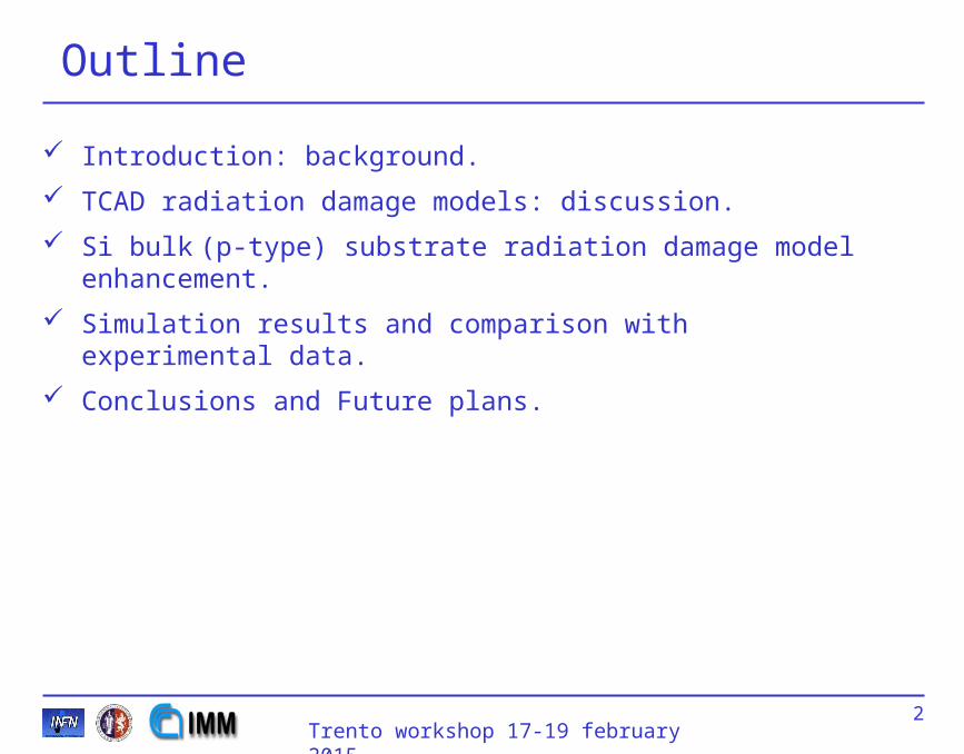
Outline
Introduction: background.
TCAD radiation damage models: discussion.
Si bulk (p-type) substrate radiation damage model enhancement.
Simulation results and comparison with experimental data.
Conclusions and Future plans.
2
Trento workshop 17-19 february 2015
“University of Perugia” model
3
Hierarchical approach based on increasing number of deep-level recombination centres / trap states.
Comprehensive modelling of device behaviour of with fluence:
- depletion voltage, leakage current (a), “double peak” shaped electric field, charge collection efficiency,…
Meaningful and physically sounded parametrization. Three levels with donor removal and increased introduction
rate (to cope with direct inter-defect charge exchange – numerically overwhelmed effect).
n type and p type substrate OK for fluences up to 1015 cm-2 1 MeV neutrons.
Trento workshop 17-19 february 2015
[1] D. Passeri, P. Ciampolini, G.M. Bilei, and F. Moscatelli, Comprehensive Modeling of Bulk-Damage Effects in Silicon Radiation Detectors, IEEE Trans. on Nuclear Science, vol. 48, no. 5, October 2001.[2] M. Petasecca, F. Moscatelli, D. Passeri, and G. U. Pignatel, Numerical Simulation of Radiation Damage Effects in p- Type and n-Type FZ Silicon Detectors, IEEE Trans. on Nuclear Science, vol. 53, no. 5, October 2006.
“University of Perugia” model (2)
More than 20 specific journal paperson TCAD radiation damage modelling
…
4
Trento workshop 17-19 february 2015
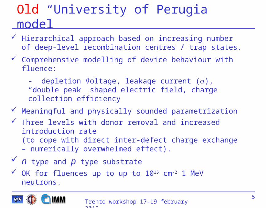
Old “University of Perugia” model
5
Hierarchical approach based on increasing number of deep-level recombination centres / trap states.
Comprehensive modelling of device behaviour with fluence:
- depletion voltage, leakage current (a), “double peak” shaped electric field, charge collection efficiency
Meaningful and physically sounded parametrization Three levels with donor removal and increased introduction
rate (to cope with direct inter-defect charge exchange – numerically overwhelmed effect).
n type and p type substrate OK for fluences up to up to 1015 cm-2 1 MeV neutrons.
Trento workshop 17-19 february 2015
Old “University of Perugia” model
6
Hierarchical approach based on increasing number of deep-level recombination centres / trap states.
Comprehensive modelling of device behaviour with fluence:
- depletion voltage, leakage current (a), “double peak” shaped electric field, charge collection efficiency
Meaningful and physically sounded parametrization Three levels with donor removal and increased introduction
rate (to cope with direct inter-defect charge exchange – numerically overwhelmed effect).
n type and p type substrate Ok for fluences up to 1015 cm-2 1 MeV neutrons.
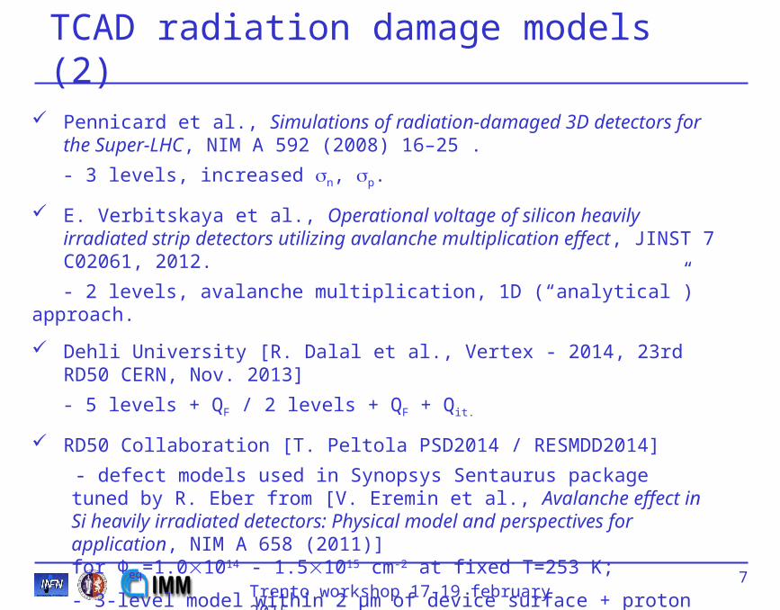
A lot of work has been done since then (see TCAD model review).
Pennicard et al., Simulations of radiation-damaged 3D detectors for the Super-LHC, NIM A 592 (2008) 16–25 .
- 3 levels, increased n, p.
E. Verbitskaya et al., Operational voltage of silicon heavily irradiated strip detectors utilizing avalanche multiplication effect, JINST 7 C02061, 2012.
- defect models used in Synopsys Sentaurus package tuned by R. Eber from [V. Eremin et al., Avalanche effect in Si heavily irradiated detectors: Physical model and perspectives for application, NIM A 658 (2011)] for Φeq=1.01014 - 1.51015 cm-2 at fixed T=253 K;
- 3-level model within 2 μm of device surface + proton model in bulk.
...
Trento workshop 17-19 february 2015
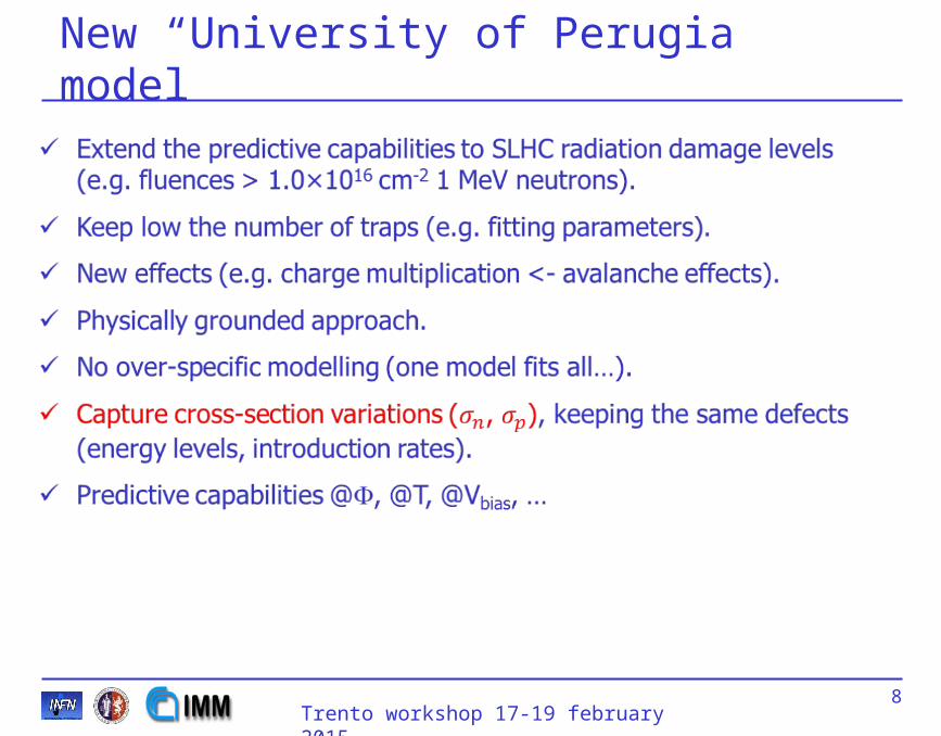
New “University of Perugia” model
8
Trento workshop 17-19 february 20159
The simulated structure
p+ ohmic contact layer effects…
p-type ND = 31012 cm-3
= 4 kohmcm depth =
300mm
Trento workshop 17-19 february 201510
The depletion voltage
The procedure used for the extraction of VDEP was the standard linear fitting cross point in the logC-logV (T=300K).
The resulting depletion voltages show a satisfactory agreement between simulation findings and experimental data [1].
[1] M. Lozano et al., Comparison of radiation hardness of P-in-N, N-in-N, and N-in-P silicon pad detectors, IEEE Trans. Nucl. Sci. 52 (5) (2005) 1468
Trento workshop 17-19 february 201511
The leakage current
The model predicts the increase of the leakage current with the fluence and the saturation of the current at full depletion voltage.
The calculated damage constant a = 3.710-17 A/cm is in good agreement with experimental data (4.0±0.1) 10-17 A/cm [2].
[2] M. Moll, Radiation damage in silicon particle detectors, Ph.D. Thesis, University of Hamburg, Hamburg, Germany (1999).
Trento workshop 17-19 february 201512
The electric field
The peculiar two-peak shape electric field profile at high fluences is reproduced.
The effect depends on the proper parametrization of the hole capture cross-sections for the VVV level (e.g. substrate effective doping variations and potential barrier at the p+ side) .
Trento workshop 17-19 february 2015
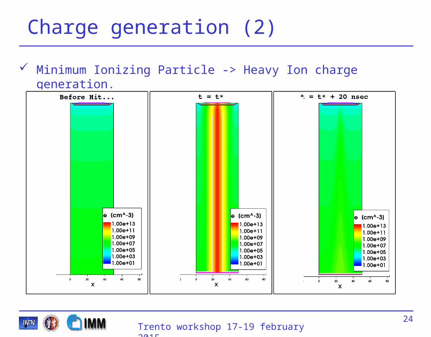
Charge generation
Heavy Ion charge generation <-> Minimum Ionizing Particle
The CCE has been evaluated by simulating a MIP crossing.
80 e/h pairs per µm in silicon.
The time varying device behavior was simulated (transient analysis), and the current at the readout electrode was integrated over 20 ns, after subtracting the leakage current, to find the total collected charge.
13
Trento workshop 17-19 february 2015
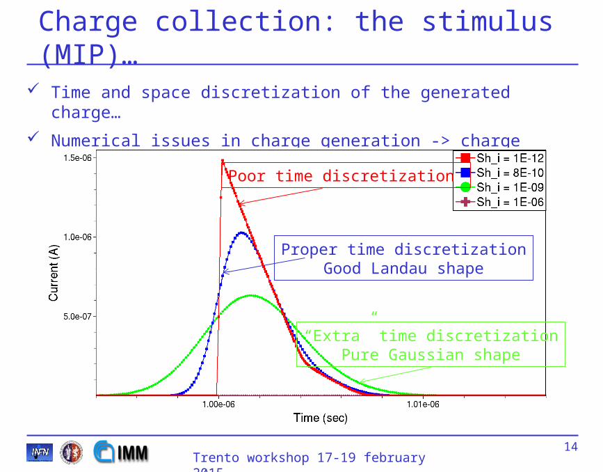
Charge collection: the stimulus (MIP)…
Time and space discretization of the generated charge…
Numerical issues in charge generation -> charge collection evaluation.
14
Poor time discretization
Proper time discretizationGood Landau shape
“Extra” time discretizationPure Gaussian shape
Trento workshop 17-19 february 201515
Charge collection at T=300K, VBIAS=900V
The charge collection behaviour at T=300K of a 280 µm-thick n-in-p strip detector was simulated in order to match the conditions used in actual measurements, e.g. [3].
ExperimentalSimulated
[3] M. Lozano et al., Comparison of radiation hardness of P-in-N, N-in-N, and N-in-P silicon pad detectors, IEEE Trans. Nucl. Sci. 52 (5) (2005) 1468
Trento workshop 17-19 february 201516
Charge collection at T=248K, VBIAS=500V
Charge collection behaviour at T=248 K of a 300 µm n-in-p [4].
[4] Affolder et al., Collected charge of planar silicon detectors after pion and proton irradiations up to 2.2x10¹⁶ neq cm2 " NIM A, Vol. 623 (2010), pp. 177-179.
VBIAS = 500V
Trento workshop 17-19 february 201517
Charge collection at T=248K, VBIAS=900V
VBIAS = 900V
[4] Affolder et al., Collected charge of planar silicon detectors after pion and proton irradiations up to 2.2x10¹⁶ neq cm2 " NIM A, Vol. 623 (2010), pp. 177-179.
Charge collection behaviour at T=248 K of a 300 µm n-in-p [4].
The effect of the avalanche generation at high fluences is pointed out.
Trento workshop 17-19 february 201518
Avalanche generation
[5] A. G. Chynoweth, Ionization Rates for Electrons and Holes in Silicon, Physical Review, vol. 109, no. 5, pp. 1537–1540, 1958.
Trento workshop 17-19 february 2015
Avalanche models
Trento workshop 17-19 february 201520
Avalanche model comparison
Fluence 2×10¹⁶
CCE (e) 4000
VanOverstraeten (def) 3900
Okuto 3800
Okuto mod a=0.8 b=0.5 3863
Okuto mod a=2.0 b=1.0 3940
Okuto mod a=5.0 b=2.0 3972
Default mod a=1.2106 3971
Default mod a=3.0106 3933
Lackner 3825
No Avalanche 2800
Trento workshop 17-19 february 201521
Charge collection at T=248 K, VBIAS=900V
VBIAS = 900V
[4] Affolder et al., Collected charge of planar silicon detectors after pion and proton irradiations up to 2.2x10¹⁶ neq cm2 " NIM A, Vol. 623 (2010), pp. 177-179.
Trento workshop 17-19 february 2015
Conclusions
22
Si bulk radiation damage modelling scheme, suitable for commercial TCAD tools (e.g. Synopsys Sentaurus).