Page 1
Ultra Wideband Power Amplifiers in 130 nm InP HBT Technology
Robert Maurer1, Seong-Kyun Kim1, Miguel Urteaga2, and Mark J. W. Rodwell1
UC Santa Barbara1
Teledyne Scientific Company2
CSICS 2016 Austin, TX
Page 2
2
Motivation
Broadly-tunable high-dynamic-range dual conversion receiver
Passive mixer IP3 determined by LO drive power
Receiver bandwidth limited by LO driver bandwidth
Page 3
3
Design Goals
Need to design a power amplifier with:
Wide bandwidth ( ~50 GHz -100 GHz)
High output power ( > 21dBm)
Preferably with:
Limited size
High power efficiency
Page 4
4
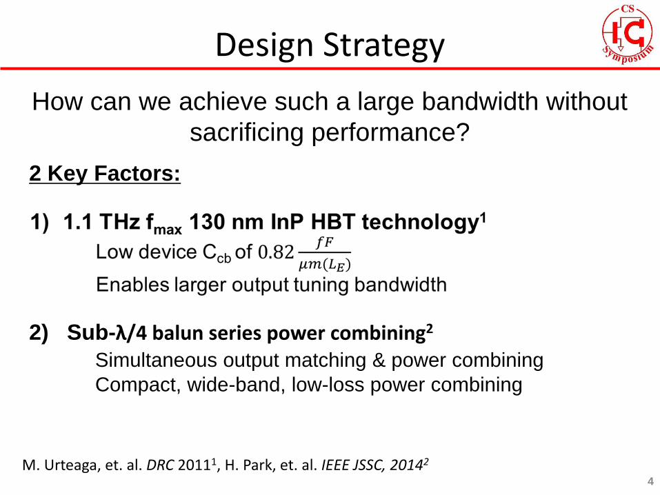
Design Strategy
How can we achieve such a large bandwidth without
sacrificing performance?
2 Key Factors:
2) Sub-λ/4 balun series power combining2
Simultaneous output matching & power combining
Compact, wide-band, low-loss power combining
M. Urteaga, et. al. DRC 20111, H. Park, et. al. IEEE JSSC, 20142
Page 5
5
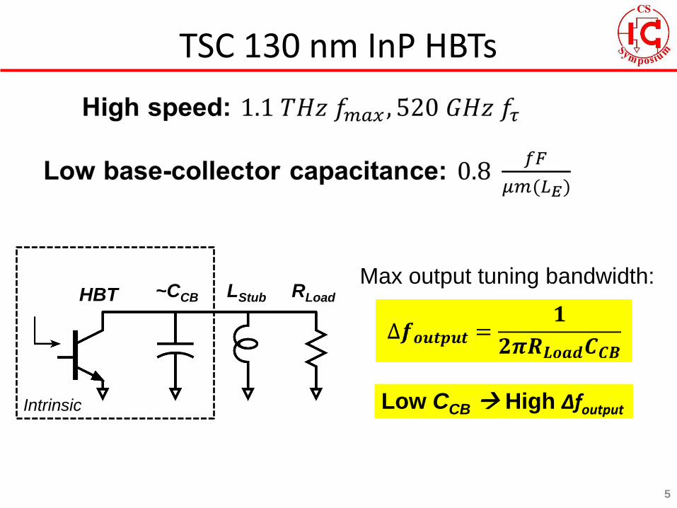
TSC 130 nm InP HBTs
Max output tuning bandwidth:
Low CCB High Δfoutput
HBT ~CCB LStub RLoad
Intrinsic
Page 6
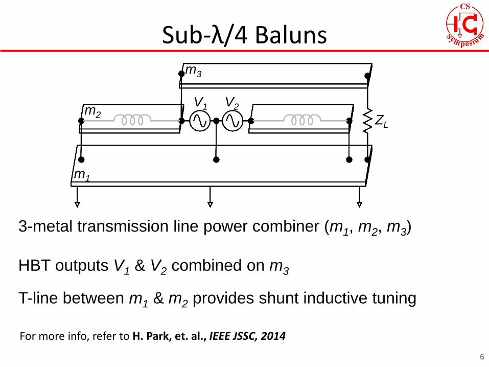
Sub-λ/4 Baluns
6
ZL
m1
m2
m3
V1 V2
3-metal transmission line power combiner (m1, m2, m3)
HBT outputs V1 & V2 combined on m3
T-line between m1 & m2 provides shunt inductive tuning
For more info, refer to H. Park, et. al., IEEE JSSC, 2014
Page 7
Amplifier Design
7
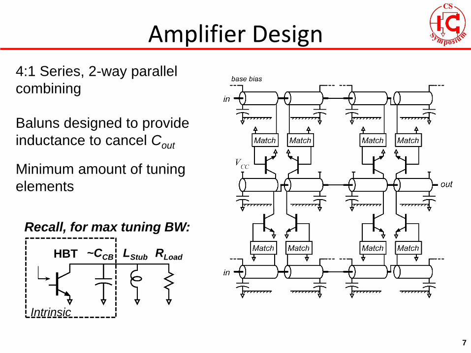
4:1 Series, 2-way parallel
combining
Baluns designed to provide
inductance to cancel Cout
Minimum amount of tuning
elements
HBT ~CCB LStub RLoad
Intrinsic
Recall, for max tuning BW:
Page 8
Pre-amplifier Stage
8
2:1 Series, 2-way parallel splitting
Designed so stage 1 outputs line
up with inputs stage 2
Provides additional gain &
eliminates need for lossy splitter
Page 9
9
Power Amplifier IC
2:1 Input Stage 4:1 Output Stage
IC Area: 0.9 mm X 1.68 mm = 1.51 mm2
Page 11
11
5
10
15
20
25
20 40 60 80 100 120
S2
1, d
B
Frequency, GHz
Measured
Simulated
-30
-25
-20
-15
-10
-5
0
20 40 60 80 100 120
mag
nitud
e, d
B
Frequency, GHz
S11
, S22
Measured
Simulated90 GHz small signal bandwidth
Broad output matching bandwidth
Input matched only near 100 GHz
Small Signal Bandwidth
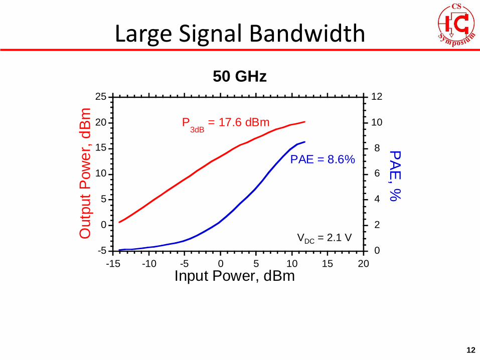
Page 12
12
-5
0
5
10
15
20
25
0
2
4
6
8
10
12
-15 -10 -5 0 5 10 15 20
Outp
ut
Pow
er,
dB
mP
AE
, %
Input Power, dBm
P3dB
= 17.6 dBm
PAE = 8.6%
50 GHz
Large Signal Bandwidth
VDC = 2.1 V
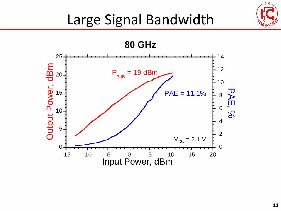
Page 13
13
0
5
10
15
20
25
0
2
4
6
8
10
12
14
-15 -10 -5 0 5 10 15 20
Outp
ut
Pow
er,
dB
mP
AE
, %
Input Power, dBm
P3dB
= 19 dBm
PAE = 11.1%
80 GHz
Large Signal Bandwidth
VDC = 2.1 V
Page 14
14
-10
-5
0
5
10
15
20
25
0
5
10
15
20
-15 -10 -5 0 5 10 15 20
Outp
ut
Pow
er,
dB
mP
AE
, %
Input Power, dBm
P3dB
= 22 dBmPAE = 14.9%
90 GHz (Peak Performance)
Large Signal Bandwidth
VDC = 2.1 V
Page 15
15
-5
0
5
10
15
20
25
0
2
4
6
8
10
12
14
16
-15 -10 -5 0 5 10 15 20
Outp
ut
Pow
er,
dB
mP
AE
, %
Input Power, dBm
P3dB
= 21.2 dBm
PAE = 13.2%
100 GHz
VDC = 2.1 V
Large Signal Bandwidth
Page 16
16
10
12
14
16
18
20
22
24
5
10
15
20
25
30
40 50 60 70 80 90 100 110
P3
dB, d
Bm
Pea
k P
AE
, %
Frequency, GHz
Large Signal Bandwidth
Measured
Simulated
PAE > 8% from 50 GHz to 100 GHz
3-dB compression of output power >15.5 dBm
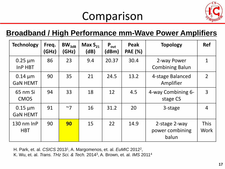
Page 17
Comparison
17
Broadband / High Performance mm-Wave Power Amplifiers
Technology Freq.(GHz)
BW3dB
(GHz)Max S21
(dB)Pout
(dBm)Peak
PAE (%)Topology Ref
0.25 μm InP HBT
86 23 9.4 20.37 30.4 2-way PowerCombining Balun
1
0.14 μm GaN HEMT
90 35 21 24.5 13.2 4-stage BalancedAmplifier
2
65 nm Si CMOS
94 33 18 12 4.5 4-way Combining 6-stage CS
3
0.15 μm GaN HEMT
91 ~7 16 31.2 20 3-stage 4
130 nm InPHBT
90 90 15 22 14.9 2-stage 2-way power combining
balun
ThisWork
H. Park, et. al. CSICS 20131, A. Margomenos, et. al. EuMIC 20122,
K. Wu, et. al. Trans. THz Sci. & Tech. 20143, A. Brown, et. al. IMS 20114
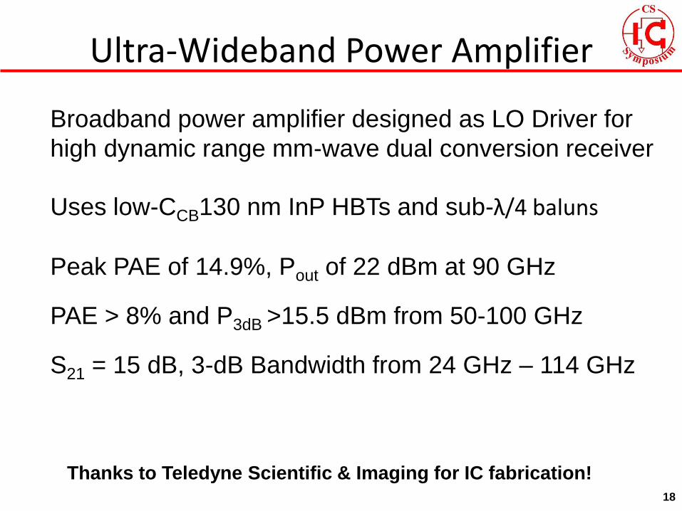
Page 18
Ultra-Wideband Power Amplifier
18
Broadband power amplifier designed as LO Driver for
high dynamic range mm-wave dual conversion receiver
Uses low-CCB130 nm InP HBTs and sub-λ/4 baluns
Peak PAE of 14.9%, Pout of 22 dBm at 90 GHz
PAE > 8% and P3dB >15.5 dBm from 50-100 GHz
S21 = 15 dB, 3-dB Bandwidth from 24 GHz – 114 GHz
Thanks to Teledyne Scientific & Imaging for IC fabrication!
Page 20
20
-5
0
5
10
15
20
25
0
5
10
15
20
-15 -10 -5 0 5 10 15 20
Outp
ut
Pow
er,
dB
mP
AE
, %
Input Power, dBm
P3dB
= 18.2 dBm
PAE = 13.2%
55 GHz
VDC = 2.145 V
Large Signal Bandwidth
Page 21
21
-5
0
5
10
15
20
25
0
2
4
6
8
10
12
14
-15 -10 -5 0 5 10 15 20
Outp
ut
Pow
er,
dB
mP
AE
, %
Input Power, dBm
P3dB
= 15.5 dBm
PAE = 8.3%
60 GHz
VDC = 2.145 V
Large Signal Bandwidth
Page 22
22
65 GHz
-5
0
5
10
15
20
25
0
2
4
6
8
10
12
-15 -10 -5 0 5 10 15 20
Outp
ut
Pow
er,
dB
mP
AE
, %
Input Power, dBm
P3dB
= 16.9 dBm
PAE = 8.2%
VDC = 2.145 V
Large Signal Bandwidth
Page 23
Ultra-Wideband Power Amplifier
23
Broadband Power amplifier uses 130 nm InP HBTs and
sub-λ/4 baluns to achieve 50-100 GHz large sig.
bandwidth
Peak PAE of 14.9%, Pout of 22 dBm at 90 GHz
PAE > 8% and P3dB >15.5 dBm from 50-100 GHz
S21 = 15 dB, 3-dB Bandwidth from 24 GHz – 114 GHz
Thanks to Teledyne Scientific & Imaging for IC fabrication!
Page 24
Sub-λ/4 Baluns
24
*H. Park, et. al., IEEE JSSC, 2014
221,0 tan jZZ stub
*
Page 25
Amplifier Design
Slide 25
4:1, 2-way power combining (4 series, 2 parallel)
Zin= (25 + jX) Ω
Determine Power
cell size
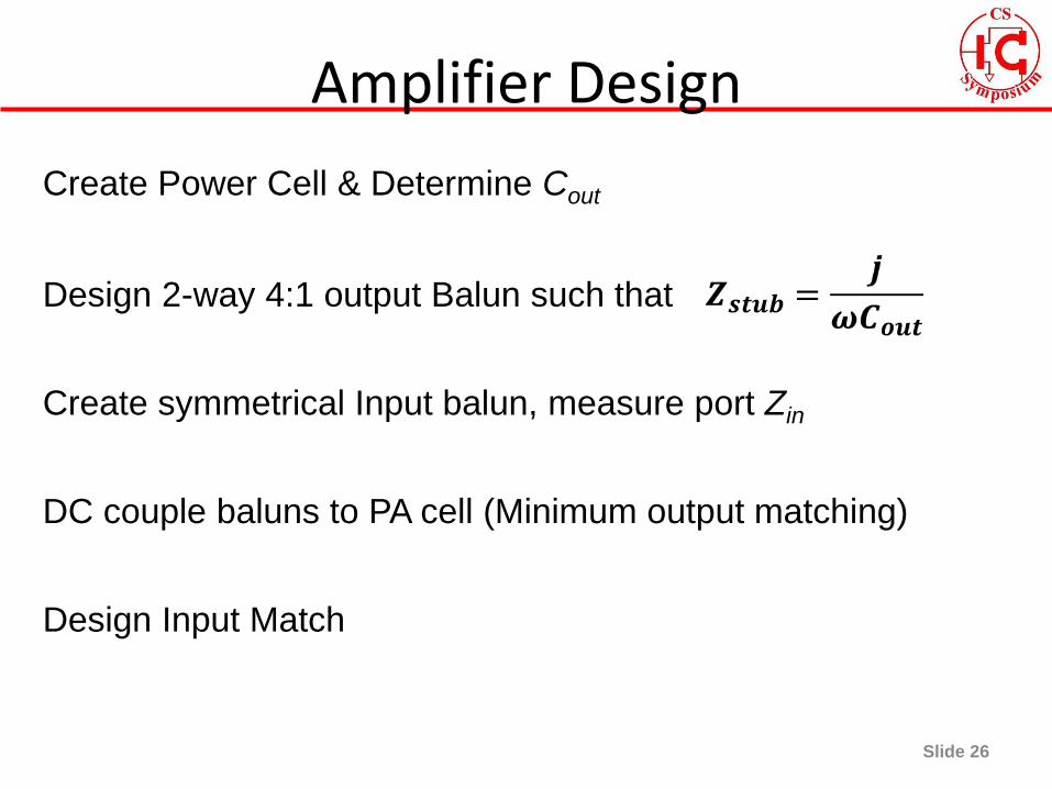
Page 26
Amplifier Design
Slide 26
Create Power Cell & Determine Cout
Design 2-way 4:1 output Balun such that
DC couple baluns to PA cell (Minimum output matching)
Create symmetrical Input balun, measure port Zin
Design Input Match
Page 27
27
TSC 130 nm InP HBTs
Max output tuning bandwidth:
Page 28
28
Design Strategy