Ultrahigh electrical conductivity in solution-sheared polymeric transparent films Brian J. Worfolk a,b , Sean C. Andrews a,b , Steve Park c , Julia Reinspach a,b , Nan Liu a , Michael F. Toney b , Stefan C. B. Mannsfeld d,1 , and Zhenan Bao a,1 a Department of Chemical Engineering, Stanford University, Stanford, CA 94305; b Stanford Synchrotron Radiation Lightsource, SLAC National Accelerator Laboratory, Menlo Park, CA 94025; c Department of Materials Science & Engineering, Stanford University, Stanford, CA 94305; and d Center for Advancing Electronics Dresden, 01187 Dresden, Germany Edited by Tobin J. Marks, Northwestern University, Evanston, IL, and approved September 29, 2015 (received for review May 21, 2015) With consumer electronics transitioning toward flexible products, there is a growing need for high-performance, mechanically robust, and inexpensive transparent conductors (TCs) for optoelectronic device integration. Herein, we report the scalable fabrication of highly conductive poly(3,4-ethylenedioxythiophene):poly(styrenesulfonate) (PEDOT:PSS) thin films via solution shearing. Specific control over deposition conditions allows for tunable phase separation and preferential PEDOT backbone alignment, resulting in record-high electrical conductivities of 4,600 ± 100 S/cm while maintaining high optical transparency. High-performance solution-sheared TC PEDOT:PSS films were used as patterned electrodes in capacitive touch sensors and organic photovoltaics to demonstrate practical viability in optoelectronic applications. transparent conductor | solution shearing | PEDOT:PSS C onductive films of high optical transparency are required in a myriad of applications, including electromagnetic shielding, antistatic layers, lighting displays, touch sensors, and as elec- trodes for photovoltaics (1, 2). As flexible, lightweight displays for televisions and portable consumer electronics become closer to reality, emerging transparent conductors (TCs) need to be mechanically robust (3). An ideal TC, therefore, should have a sheet resistance <100 Ω/□, transmissivity greater than 0.90, and be inherently flexible, all while remaining inexpensive to process on a mass scale (4). Indium tin oxide (ITO) is the most widely used TC material due to the combination of low sheet resistance and high trans- parency when grown on a variety of substrates. Although com- mon to use, ITO is an expensive material due to the requirement for vacuum deposition and a number of postprocessing steps (5). For example, in organic photovoltaic (OPV) modules ITO was estimated to represent 24% of the module cost (6). However, alternative transparent conductor materials, such as poly(3,4- ethylenedioxythiophene):poly(styrenesulfonate) (PEDOT:PSS) are estimated to comprise only ∼1% of an OPV module cost. Additionally, ITO is not compatible with flexible applications, because small applied strains of as little as 4.5% lead to an order of magnitude increase in the resistance (7). In recent years there have been a number of emerging TC ma- terials studied in the literature ranging from metal nanowires (Au, Ag, Cu) (8– 11), conducting carbon allotropes (graphene, carbon nanotubes) (12–15), conducting polymers (16, 17), and other hybrid approaches (18). Recent attempts using metal nanotroughs by Wu et al. have resulted in superior optoelectronic properties with a sheet resistance of 2 Ω/□ at 90% transmission (19). The use of metal mesoscale grids further enhanced the properties of metal nanowires electrodes to a sheet resistance of 0.36 Ω/□ at 92% transmission (20). Although metal nanowires combine low resistance and high transparency, they have inferior flexibility and stretchability com- pared with polymer-based TCs (3). PEDOT:PSS consists of insoluble PEDOT that is charge stabi- lized by PSS (Fig. 1A), which affords good solubility in aqueous formulations. Within these solutions, PEDOT:PSS forms micelles where hydrophilic PSS is in contact with water and hydrophobic PEDOT is located in the micelle core (21). Upon spin-coating from solution, the micelles are deposited as a film and can have conductivities on the order of ∼1 S/cm (22). Subsequent annealing, treatment with cosolvents, and postprocessing steps can increase the conductivity of films to over 3,000 S/cm (23, 24). High-performing spin-cast PEDOT:PSS TCs have reached a sheet resistance of 46 Ω/□ at 90% transmission (25, 26). Furthermore, it is compatible with flexible electronics as films can withstand over 90% applied strain without electrical breakdown (7). There is a wide variety of solution processing techniques used to deposit uniform, low-roughness films (27). Spin-casting is a popular laboratory-scale deposition technique due to its simplicity and ability to deposit high-quality films with a variety of materials. However, it is a batch process that is difficult to implement on a continuous mass production scale. Furthermore, it is difficult to use elevated substrate temperatures during spin-coating, a parameter that may play a role in the final film characteristics. Contrarily, scalable fabrication through solution shearing allows for tunable deposition conditions which enable enhanced kinetic control resulting in large impacts on the electrical performance of organic electronics (28– 30). In this work we use solution shearing to fabricate high- performance TC PEDOT:PSS films (Fig. 1B). Tunable control of PEDOT backbone orientation, local ordering, and phase sepa- ration is demonstrated via precise control of the deposition pa- rameters. Record-high PEDOT:PSS conductivities of 4,600 ± 100 S/cm are obtained and reach a sheet resistance of 17 ± 1 Ω/□ at 97.2 ± 0.4% transmission. A patterning method (Fig. 1C) is also developed which enables the use of high-conductivity Significance Many applications, including solar cells and touch screens, re- quire coatings that are both optically transparent and electri- cally conductive. Most device structures use indium tin oxide to serve as this transparent conductor (TC), even though it accounts for a disproportionally large amount of device cost. Alternatives, such as polymer-based materials, may not only provide additional cost benefits, but may also allow for added functionality, such as flexibility. In this paper, we examine conductive poly(3,4-ethylenedioxythiophene):poly(styrenesul- fonate) (PEDOT:PSS) deposited by solution shearing as a TC film. Morphological and chemical changes caused by solution shearing deposition lead to record-high conductivities and overall excellent TC performance. Author contributions: S.C.B.M. and Z.B. designed research; B.J.W., S.C.A., S.P., and N.L. performed research; B.J.W., S.C.A., J.R., and M.F.T. analyzed data; and B.J.W. and S.C.A. wrote the paper. The authors declare no conflict of interest. This article is a PNAS Direct Submission. 1 To whom correspondence may be addressed. Email: [email protected] or [email protected]. This article contains supporting information online at www.pnas.org/lookup/suppl/doi:10. 1073/pnas.1509958112/-/DCSupplemental. 14138–14143 | PNAS | November 17, 2015 | vol. 112 | no. 46 www.pnas.org/cgi/doi/10.1073/pnas.1509958112
Transcript
Ultrahigh electrical conductivity in solution-shearedpolymeric transparent filmsBrian J. Worfolka,b, Sean C. Andrewsa,b, Steve Parkc, Julia Reinspacha,b, Nan Liua, Michael F. Toneyb,Stefan C. B. Mannsfeldd,1, and Zhenan Baoa,1
aDepartment of Chemical Engineering, Stanford University, Stanford, CA 94305; bStanford Synchrotron Radiation Lightsource, SLAC National AcceleratorLaboratory, Menlo Park, CA 94025; cDepartment of Materials Science & Engineering, Stanford University, Stanford, CA 94305; and dCenter for AdvancingElectronics Dresden, 01187 Dresden, Germany
Edited by Tobin J. Marks, Northwestern University, Evanston, IL, and approved September 29, 2015 (received for review May 21, 2015)
With consumer electronics transitioning toward flexible products,there is a growing need for high-performance, mechanically robust,and inexpensive transparent conductors (TCs) for optoelectronicdevice integration. Herein, we report the scalable fabrication of highlyconductive poly(3,4-ethylenedioxythiophene):poly(styrenesulfonate)(PEDOT:PSS) thin films via solution shearing. Specific control overdeposition conditions allows for tunable phase separation andpreferential PEDOT backbone alignment, resulting in record-highelectrical conductivities of 4,600 ± 100 S/cm while maintaininghigh optical transparency. High-performance solution-shearedTC PEDOT:PSS films were used as patterned electrodes in capacitivetouch sensors and organic photovoltaics to demonstrate practicalviability in optoelectronic applications.
Conductive films of high optical transparency are required in amyriad of applications, including electromagnetic shielding,
antistatic layers, lighting displays, touch sensors, and as elec-trodes for photovoltaics (1, 2). As flexible, lightweight displaysfor televisions and portable consumer electronics become closerto reality, emerging transparent conductors (TCs) need to bemechanically robust (3). An ideal TC, therefore, should have asheet resistance <100 Ω/□, transmissivity greater than 0.90, andbe inherently flexible, all while remaining inexpensive to processon a mass scale (4).Indium tin oxide (ITO) is the most widely used TC material
due to the combination of low sheet resistance and high trans-parency when grown on a variety of substrates. Although com-mon to use, ITO is an expensive material due to the requirementfor vacuum deposition and a number of postprocessing steps (5).For example, in organic photovoltaic (OPV) modules ITO wasestimated to represent 24% of the module cost (6). However,alternative transparent conductor materials, such as poly(3,4-ethylenedioxythiophene):poly(styrenesulfonate) (PEDOT:PSS)are estimated to comprise only ∼1% of an OPV module cost.Additionally, ITO is not compatible with flexible applications,because small applied strains of as little as 4.5% lead to an orderof magnitude increase in the resistance (7).In recent years there have been a number of emerging TC ma-
terials studied in the literature ranging from metal nanowires (Au,Ag, Cu) (8–11), conducting carbon allotropes (graphene, carbonnanotubes) (12–15), conducting polymers (16, 17), and other hybridapproaches (18). Recent attempts using metal nanotroughs by Wuet al. have resulted in superior optoelectronic properties with a sheetresistance of 2 Ω/□ at 90% transmission (19). The use of metalmesoscale grids further enhanced the properties of metal nanowireselectrodes to a sheet resistance of 0.36 Ω/□ at 92% transmission(20). Although metal nanowires combine low resistance and hightransparency, they have inferior flexibility and stretchability com-pared with polymer-based TCs (3).PEDOT:PSS consists of insoluble PEDOT that is charge stabi-
lized by PSS (Fig. 1A), which affords good solubility in aqueousformulations. Within these solutions, PEDOT:PSS forms micelles
where hydrophilic PSS is in contact with water and hydrophobicPEDOT is located in the micelle core (21). Upon spin-coatingfrom solution, the micelles are deposited as a film and can haveconductivities on the order of ∼1 S/cm (22). Subsequent annealing,treatment with cosolvents, and postprocessing steps can increase theconductivity of films to over 3,000 S/cm (23, 24). High-performingspin-cast PEDOT:PSS TCs have reached a sheet resistance of46Ω/□ at 90% transmission (25, 26). Furthermore, it is compatiblewith flexible electronics as films can withstand over 90% appliedstrain without electrical breakdown (7).There is a wide variety of solution processing techniques used to
deposit uniform, low-roughness films (27). Spin-casting is a popularlaboratory-scale deposition technique due to its simplicity and abilityto deposit high-quality films with a variety of materials. However, it isa batch process that is difficult to implement on a continuous massproduction scale. Furthermore, it is difficult to use elevated substratetemperatures during spin-coating, a parameter that may play a rolein the final film characteristics. Contrarily, scalable fabricationthrough solution shearing allows for tunable deposition conditionswhich enable enhanced kinetic control resulting in large impacts onthe electrical performance of organic electronics (28–30).In this work we use solution shearing to fabricate high-
performance TC PEDOT:PSS films (Fig. 1B). Tunable control ofPEDOT backbone orientation, local ordering, and phase sepa-ration is demonstrated via precise control of the deposition pa-rameters. Record-high PEDOT:PSS conductivities of 4,600 ±100 S/cm are obtained and reach a sheet resistance of 17 ± 1 Ω/□at 97.2 ± 0.4% transmission. A patterning method (Fig. 1C) isalso developed which enables the use of high-conductivity
Significance
Many applications, including solar cells and touch screens, re-quire coatings that are both optically transparent and electri-cally conductive. Most device structures use indium tin oxideto serve as this transparent conductor (TC), even though itaccounts for a disproportionally large amount of device cost.Alternatives, such as polymer-based materials, may not onlyprovide additional cost benefits, but may also allow for addedfunctionality, such as flexibility. In this paper, we examineconductive poly(3,4-ethylenedioxythiophene):poly(styrenesul-fonate) (PEDOT:PSS) deposited by solution shearing as a TCfilm. Morphological and chemical changes caused by solutionshearing deposition lead to record-high conductivities andoverall excellent TC performance.
Author contributions: S.C.B.M. and Z.B. designed research; B.J.W., S.C.A., S.P., and N.L.performed research; B.J.W., S.C.A., J.R., and M.F.T. analyzed data; and B.J.W. and S.C.A.wrote the paper.
transparent conductive films in capacitive pressure sensors andOPV devices.
Results and DiscussionProperties of Solution-Sheared PEDOT:PSS Transparent Conductors.The effects of shearing speed and temperature on the electronicproperties of PEDOT:PSS films are shown in Fig. 2A. At 65 °Cthere is a sharp increase in the sheet resistance of films withfaster shearing speeds. This is consistent with depositing thinnerfilms at higher shearing speeds, resulting in higher resistances.However, when the substrate temperature is increased to 85 °C,there is a near-flat response between increasing shearing speedand sheet resistance. PEDOT:PSS film thickness decreases from95 ± 2 nm to 41 ± 2 nm when increasing the shearing speed from0.5 to 1.5 mm/s. The film thickness then begins to increase at2 mm/s (53 ± 2 nm) shearing speeds, signaling the PEDOT:PSSprocessing changes from the evaporative to the Landau–Levichregime (31). Fig. 2B illustrates the effect of shearing speed onthe transmissivity at 550 nm of PEDOT:PSS films at 65 and85 °C. The film transmission ranges from 83.5 ± 0.2% to 97.1 ±0.2% for increasing shearing speed from 0.5 to 1.5 mm/s. Be-cause the film thickness begins to increase at 2 mm/s, the cor-responding film transparency also begins to decrease to 96.5 ±0.3%. Tuning the temperature and shearing speed allows for
optimization of film thickness, as well as the resulting sheet re-sistance and transparency.Recently there have been a number of methods reported to
improve the transparent conductor properties of PEDOT:PSS.Fig. 2C illustrates some of the highest performance PEDOT:PSStransparent conductor films using a Zonyl fluorosurfactant (lightblue open diamonds) (16), posttreatment with methanol (greenopen squares) (22), and sulfuric acid (brown open triangles) (23).Repeating spin-coated PEDOT:PSS films and posttreatmentwith methanol (purple open squares) yields similar performanceas the previously reported literature (22). However, shearedPEDOT:PSS films at both 65 °C (blue solid squares) and 85 °C(red solid circles) outperform spin-coated films (all methanoltreated), combining a beneficial decrease in sheet resistance withimproved transparency. Sheared PEDOT:PSS films at 85 °Chave superior performance and lead to more reliable depositionof films, as evident in the tighter clustering of data points. Fig.2D plots the effect of shearing speed on film conductivity de-posited at 85 °C. Single-layer conductivity peaks at 0.75 mm/s,but when the thickness is increased by depositing a second layerof PEDOT:PSS, the optimal conductivity occurs at a shearingspeed of 3 mm/s. For double-layered films, the drop in conduc-tivity with further increasing or decreasing the shearing speed isminimal compared with single-layered films.The figure of merit (FoM) for transparent conductors is de-
fined as the ratio of direct current conductivity (σdc) to opticalconductivity (σop):
FoM=σdc
σopðλÞ=188.5 Ω
Rsheet
�TðλÞ−1=2 − 1
�,
where Rsheet is the sheet resistance and T is the transmittance atλ = 550 nm. Typically an FoM greater than 35 is a minimumbenchmark indicating commercial viability of transparent conduc-tors (4). This constitutes a sheet resistance ≤100 Ω/□ and trans-parency ≥90%. The FoM for single- and double-layered shearedPEDOT:PSS films are shown in Fig. 2D. The FoM for all shearedfilms was in excess of 35 and reached 286 for double-layered
Fig. 1. Schematic of solution shearing process. (A) Chemical structure ofPEDOT:PSS. (B) Schematic of the solution shearing design and (C) patterningPEDOT:PSS via selective patterning of solvent wetting and dewetting regions.
Fig. 2. PEDOT:PSS as a transparent conductor. The effect of coating speed on the sheet resistance (A) and transmittance (B) of PEDOT:PSS films on glasssubstrates sheared at 65 °C and 85 °C. (C) The sheet resistance and transmittance of PEDOT:PSS films sheared and spin-cast compared with literature reports ofPEDOT:PSS treated with methanol (22), H2SO4 (23), and a Zonyl fluorosurfactant (16). (D) The conductivity and σdc/σop ratio of single- and double-layeredPEDOT:PSS films sheared at 85 °C and treated with MeOH.
Worfolk et al. PNAS | November 17, 2015 | vol. 112 | no. 46 | 14139
APP
LIED
PHYS
ICAL
SCIENCE
S
PEDOT:PSS films sheared at 3 mm/s (Supporting Information).This dramatically surpasses the previous highest FoM for PEDOT:PSS transparent conductors which had an FoM of 72 for H2SO4treated films (Rsheet = 46 Ω/□ and T = 0.90) (23). PEDOT:PSSsolution sheared at 2.5 mm/s and treated with methanol results infilms with Rsheet = 38 Ω/□ at 96% transmission for an FoM of 232.Spin-coated PEDOT:PSS films treated with methanol have Rsheet =112 Ω/□ with 92% transmission, a conductivity of 891 S/cm, andFoM = 39. Shearing PEDOT:PSS greatly improves the opticaltransparency while also decreasing the sheet resistance, enablingfilms to surpass the FoM of typical alternative transparentconductors.
Characterization of PEDOT:PSS Films. To decipher the different ef-fects the deposition techniques have on the film morphology, weprepared a series of spin-cast and sheared films on Si and imagedthem using scanning electron microscopy (SEM) and atomic forcemicroscopy (AFM). The SEM and AFM images in Fig. 3 show thatspin-cast films treated with methanol show very small sphericalparticles somewhat assembled into ill-defined short nanofibers.However, sheared films show more prominent well-defined fiberswhich become elongated with faster shearing speeds. Whereasthe sheared nanofibers do not appear to have any preferentialarrangement in the direction of shearing according to these images,the fibrous networks form an interconnected mesh network whichmay enable superior charge transport.Treatment of PEDOT:PSS spin-cast films with methanol has
shown to increase phase segregation between PEDOT and PSSdomains and reduce excess PSS content as evidenced through X-rayphotoelectron spectroscopy (XPS) surface scans (22). Althoughsurface XPS acquisitions can provide valuable information, beingable to probe the chemical composition through the bulk of the filmcan reveal whether vertical compositional gradients are present.High-resolution XPS of the S 2p region of PEDOT:PSS comprisestwo peaks: the sulfonate moiety from PSS occurs at higher bindingenergy and the thiophene in PEDOT appears at lower bindingenergy (Supporting Information) (32).XPS depth profiles in Fig. 4 A and B show different vertical phase
gradients between the two deposition techniques (example spectracan be seen in Supporting Information). The yellow boxes on theplots highlight the areas of significant difference in the verticalcomposition of films. Spin-coated films are PSS-rich but quicklychange to a near 1:1 ratio of PSS:PEDOT throughout the bulk ofthe film (Fig. 4A). For sheared films, the top half is dominated byPSS, whereas the bottom half is dominated by PEDOT (Fig. 4B).Sheared films exhibit a greater extent of phase separation, wherethe PSS surface has segregated from the PEDOT-rich layer beneath
(Supporting Information). This reduction of PSS content in thebottom half of the film increases the conductivity near the substrateinterface. Additionally, sheared films with higher PSS surface con-centration can aid in its removal from the films, increasingconductivity.Polarized UV-visible (UV-vis) spectroscopy was used to ex-
tensively characterize the transparency and electronic transitions,the latter of which can be correlated to molecular ordering andaggregation in thin polymer films (33). Unpolarized absorptionin sheared films reveals a weak, broad feature occurring near800 nm, a feature not present in spin-cast films (Fig. 5C). Thiselectronic transition has been observed in doped PEDOT (34),indicating the existence of a highly conductive phase in solution-sheared films. This indicates that the solution shearing depositionprocess, while better allowing the removal of excess PSS near thesurface, also maintains the potency of the remaining PSS dopants.Furthermore, s-polarized absorption does not exhibit this transi-tion, whereas it is clearly observed with p polarization. The an-isotropic nature of the solution shearing process imparts anisotropicstructure within the deposited PEDOT:PSS film, preferentiallyaligning the conductive PEDOT species. The degree of alignmentcan be compared with the dichroic ratio of the p-/s-polarized ab-sorption at 800 nm. This was determined for shearing speeds of0.5, 1, and 3 mm/s as well as for spin-cast films. As seen in Fig. 5D,all sheared films have a dichroic ratio greater than 1, whereas thespin-cast film is close to 1. Additionally, the magnitude of alignmentincreases with increasing shearing speed, with 3 mm/s exhibiting the
Fig. 3. PEDOT:PSS film morphology. SEM (A) and AFM phase images (B) ofPEDOT:PSS spin-cast at 1,000 rpm and sheared films at 0.5 and 3 mm/s afterall were annealed and treated with methanol.
Fig. 4. Differences in PEDOT:PSS film composition. High-resolution XPS C60 iongun sputtering profiles of spin-cast (A) and sheared (B) PEDOT:PSS at 3 mm/s.
14140 | www.pnas.org/cgi/doi/10.1073/pnas.1509958112 Worfolk et al.
highest ratio. This speed corresponds with the optimized conditionsfor maximized double-layer FoM.To help elucidate the mechanism of increased conduction
via solution shearing and MeOH postprocessing treatment,temperature-dependent conductivity was measured. As seen in Fig.6, treatment with MeOH increases conductivity in both samples byover 2 orders of magnitude, with the solution-sheared films con-tinuing to exhibit higher overall conductivity. Additionally, twoslopes are clearly observed above/below 160 K in MeOH-treatedsolution-sheared films, indicating a switching of the dominant holescattering process below that temperature. The change is moreclearly seen in the Arrhenius plot (Fig. 6, Inset). It has recently beenshown that solvent-treated films can increase the ordering andshorten interpolymer distances (35). Whereas the MeOH treatmentis having similar effects on the PEDOT:PSS films, the increasedordering provided by the solution shearing process gives way to thefurther enhanced electrical transport properties.
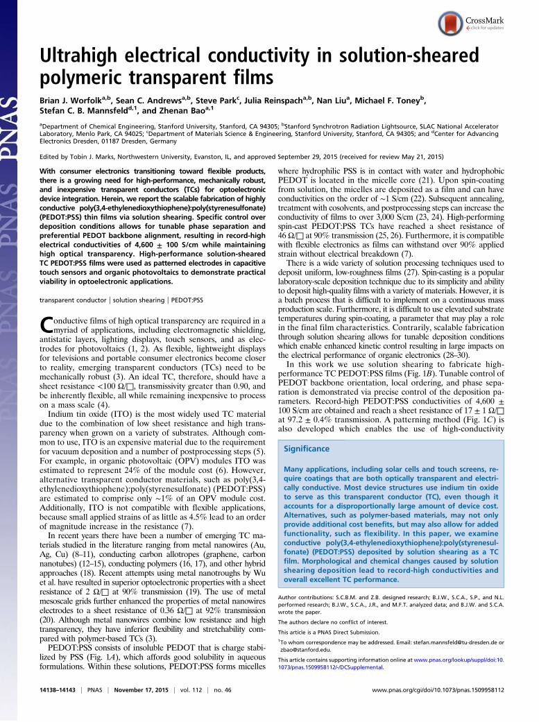
Applied Devices and Patterning. The high conductivity of thesolution-sheared PEDOT:PSS film renders it a viable material asa transparent conductor in various devices. Specifically, the high-quality interface it can provide was demonstrated in OPV devices.Highly conductive sheared PEDOT:PSS films was applied asthe anode in OPV devices, where the device architecture con-tained a poly(3-hexylthiophene) (P3HT): [6,6]-phenyl-C61-butyricacid methyl ester (PC61BM) photoactive layer and LiF/Al cathode.The current density–voltage (J–V) plots are shown in Fig. 7A andphotovoltaic characteristics in Supporting Information.Sheared PEDOT:PSS electrodes obtained a power conversion
efficiency (PCE) of 2.87%, which was similar to using ITO TCs(2.86%). The ITO electrodes had higher open-circuit voltages(VOC) and short-circuit current densities (JSC), but a lower fillfactor (FF). High fill factors for sheared PEDOT:PSS devicescan be attributed to the low sheet resistance of TC films, andpotentially improved bulk heterojunction morphology in thephotoactive layer. Spin-cast PEDOT:PSS films had a PCE of2.20% with lower JSC and FF compared with sheared films. Thereduction in these photovoltaic parameters is the result of highsheet resistance and lower transparency of spin-cast PEDOT:PSSTCs. The similar photovoltaic performance of sheared PEDOT:PSSand ITO transparent electrodes indicates that solution-shearedPEDOT:PSS electrodes could be a cost-effective alternative toITO in OPV devices.Whereas some applications require conformal coatings, lateral
patterning of electrodes is important for fabricating some devicestructures, such as circuits and sensors. Here, a simple techniquewas developed to deposit the PEDOT:PSS films into patterns,preventing the need for postdeposition lithographic processesthat can damage the film. Before shearing, defined patterns ofhydrophillic and hydrophobic areas (see Materials and Methodsfor details) are prepared on the substrate surface (36). As thePEDOT:PSS solution is sheared, the meniscus is confined andpinned within the hydrophillic region, resulting in selective filmdeposition. Fig. 7B is an optical image of patterned PEDOT:PSSfilm. Line width and spacing as small as 2 μm are achievable withthis methodology.
Fig. 5. Optical anisotropy in solution-sheared films. Polarized UV-vis absorption of spin-cast (A) and sheared PEDOT:PSS films (85 °C) at 3 mm/s (B). Directcomparison of nonpolarized absorption in sheared and spin-cast films (C). The dichroic ratio of spin-cast and sheared films deposited with a blade speed of0.5, 1, and 3 mm/s (D).
Fig. 6. Temperature-dependent conductivity. Temperature responses of solu-tion-sheared (85 °C) and spin-coated PEDOT:PSS film before and after treatmentwith methanol. (Inset) Arrhenius plot of both solution-sheared and spin-coatedfilms after MeOH treatment. The dotted line is a guide to the eye.
Worfolk et al. PNAS | November 17, 2015 | vol. 112 | no. 46 | 14141
One possible application of patterned electrodes is two-dimensional position pressure sensing. To demonstrate this con-cept, 10 electrodes were patterned in parallel on polyethyleneterephthalate (PET) with width and spacing of 5 mm. Apolydimethylsiloxane (PDMS) spacer separated two coated PETsubstrates aligned perpendicular to each other (Fig. 7D, Top). Themiddle pixel (5, 5) was then pressed at a pressure of 50 kPa, andthe change in capacitance was measured for all of the arrays. Fig.7C is a contour map showing the change in capacitance over theentire array. Fig. 7D contains a plot of change in capacitance versustime at various pixels away from the pixel being pressed at apressure of 50 kPa. The change in capacitance is the highest at thepixel being pressed. This simple example demonstrates the feasi-bility of using flexible, patterned electrodes in similar architecturessuch as active-matrix organic light-emitting diode displays and radio-frequency identification tags.In conclusion, we have used a scalable deposition technique for
the fabrication of high-performance polymer transparent conduc-tors. Control of the solution shearing parameters results in record-high PEDOT:PSS conductivity of 4,600 ± 100 S/cm with a sheetresistance of 17 ± 1 Ω/□ at 97.2 ± 0.4% transmission. Tuning theshearing conditions allows for kinetic control over film depositionmorphology, composition, and anisotropy. Solution-sheared filmsoutperform spin-coated films in all aspects of FoM and applieddevice performance. Additionally, solution shearing allows forpatterned deposition, with a demonstrated resolution of 2 μm. Thispatterning of TCs allows use in a variety of applications includingcapacitive touch sensors, transistors, and OPVs. This study estab-lished PEDOT:PSS as a low-cost and mechanically robust alter-native to ITO transparent conductors.
Materials and MethodsMaterials. PEDOT:PSS formulations: PH1000 and PVP AI 4083 were purchasedfrom Heraeus. P3HT P200 was obtained from Rieke Metals and PC61BM was
acquired from nano-C. Methanol, 2-propanol, 1,2-dichlorobenzene, andlithium fluoride were used as received from Sigma-Aldrich.
Solution Shearing PEDOT:PSS Films. PEDOT:PSS films were sheared on glass, Si,Si/SiO2, and PET substrates. Substrates were rinsedwith 2-propanol and exposedto a 5-min O2 plasma (1 min for PET substrates) at 150 W with 200 mtorr of O2
pressure. Films were deposited at 65 °C and 85 °C on a temperature-controlledshearing stage. The Si shearing blade was functionalized with a highly crystal-line monolayer of octadecyltrichlorosilane according to our previously pub-lished methods (37). The shearing blade was orientated completely parallel tothe substrate. A gap height of 100 μm was used between the substrate andshearing blade. PEDOT:PSS was coated at speeds of 0.02–4 mm/s, producingfilms with a range of thickness from 20 nm to over 250 nm. Films were thenplaced on a hotplate at 130 °C and methanol dropped on top, covering thePEDOT:PSS film. The film was annealed for 10 min, cooled to room tempera-ture, and rinsed with methanol. Once again, the substrate was annealed for10 min at 130 °C. For double-layered films, methanol treatment was performedafter the first deposited layer before shearing the second layer on top (andsubsequent methanol treating).
Spin-Cast PEDOT:PSS Films. Spin-cast PEDOT:PSS was performed on the samesubstrates as sheared films. PEDOT:PSSwas filteredwith a 0.2-μmmixed celluloseacetate filter directly onto substrates and spin-coated at 1,000–4,000 rpm for60 s. Films had the same methanol treatment procedure as sheared films.
Instrumental. AFM images were recorded in tapping mode using a VeecoMultimodeAFM. The resistance of filmswasmeasured using four-point probewith collinear probes of 0.5-cm spacing, and tested using a Keithley 2400source meter. The resistance of sheared films was measured perpendicularto the shearing direction, unless otherwise noted. SEM was performed withan FEI Magellan 400 XHR SEM with an acceleration voltage of 700 V. UV-visabsorption was taken with a Cary 6000i spectrophotometer. An aperturemeasuring 1.3 × 0.4 cm was used for all measurements. Transmission valuesthroughout the paper were recorded at 550 nm. Film thicknesses weremeasured using a contact probe Dektak 150 profilometer. All thicknessvalues were the average of at least three measurements in different areas ofthe film. Typically depth profiling XPS uses an Ar ion sputtering gun which isdestructive in organic films often losing valuable chemical information. Spin-cast and sheared films on Si were analyzed with a C60 ion sputtering gun
Fig. 7. Application of solution-sheared PEDOT:PSS. (A) Current density–voltage curves for organic photovoltaic devices with PEDOT:PSS or ITO anodes.(B) Optical image of 10-μm PEDOT:PSS lines deposited on a patterned substrate. (C) The change in capacitance of a flexible PEDOT:PSS pressure sensor whenpixel (5, 5) is pressed with a pressure of 50 kPa. (D, Top) Optical image of the interdigitated electrodes used for pressure sensor in C. (D, Bottom) The responseof neighboring pixels when a PEDOT:PSS pressure sensor point is pressed and released with 50 kPa of pressure.
14142 | www.pnas.org/cgi/doi/10.1073/pnas.1509958112 Worfolk et al.
which allows for considerably gentler sputtering while often preservingchemical information in organic films. XPS was performed with a PHIVersaProbe Scanning XPS Microprobe with a 1,486-eV Al Kα photon sourcewith 100-μm spot size (100 W, 20 kV). Sputtering was performed at 10 kVand 20 mA over a spot size of 2 × 2 mm. Grazing incidence wide angle X-rayspectroscopy (GIWAXS) was performed at Stanford Synchrotron RadiationLightsource at beamline 11–3. Analysis and integration of diffraction datawere analyzed using WxDiff (38).
Six 50-nm-thick patterned Au electrodes were thermally deposited on Si/SiO2
(300-nm oxide thickness) substrates with a width of 7,500 μm and length of500 μm, and PEDOT:PSS was spin-coated or sheared on top. To account forcontact resistance, the four-probe method was used. The conductivity was cal-culated for each electrode measurement according to the following calculation:σdc = 1
Rsheet t, where t is the film thickness. The average of at least four conductivity
measurements (with different electrode spacings) is reported in this article.
Patterning of PEDOT:PSS Films and Transistor Fabrication. To generate smallline features of PEDOT:PSS film, photolithographywas used to generate strips ofphotoresist on a silicon substrate. The surface was then treated with O2 plasmafor 30 s at 150W to activate the SiO2 surface. The substrate was then placed in adesiccator with a vial filled with 50 μL of tridecafluoro-1,1,2,2-tetrahydrooctyltrichlorosilane (fluorosilane) for 3 h (39). Thereafter, the photoresist was re-moved by soaking the substrate in acetone under sonication for 1 h. Thesubstrate was then taken out of acetone, washed with isopropyl alcohol, anddried with nitrogen gas. To generate larger features of PEDOT:PSS film, asubstrate (glass, PET, or silicon) was firstly treated with O2 plasma andfluorosilane, as described above. Then a metallic shadow mask with desiredfeatures was placed on top of the substrate, and the substrate was treated brieflywith O2 plasma for 10 s at 150W. The fluorosilane was removed where there wasan opening, resulting in patterned hydrophobic and hydrophillic regions.
Device Fabrication. Position pressure sensors were fabricated by shearingPEDOT:PSS film on PET substrates with an array of 10 hydrophillic lines inparallel. The linewidth and spacingwere 5mm. Two PET substrates were then
placed on top of each other with the PEDOT:PSS films facing inward, andwiththe electrode arrays oriented perpendicular to each other. PDMS spacers2 mm in diameter and 1 mm thick were placed between every other pixel.The electrodes were wired out using copper tape.
OPV devices were fabricated on sheared PEDOT:PSS (with and withoutmethanol treatment), spin-cast PEDOT:PSS, and ITO substrates. For ITOsubstrates, PEDOT:PSS (AI PVP 4083) was filtered with a 0.2-μm mixed cel-lulose acetate filter directly on the substrate and was spin-cast at 3,000 rpmfor 1 min. The film was then annealed at 140 °C for 10 min. The photoactivelayer solution was prepared from a 1:1 mass ratio of P3HT and PC61BM at atotal weight concentration of 50 mg/mL in o-dichlorobenzene and stirredovernight at 40 °C. The photoactive blend solution was spin-cast in air on topof the appropriate TC substrate at 600 rpm for 1 min and placed in a coveredPetri dish to dry for 20 min in air. Substrates were then loaded into a thermalevaporator and top contacts were deposited at a pressure <1 × 10⁻⁵ torr;0.4 nm of LiF at 0.1 Å/s, and 50 nm of Al at 1–4 Å/s were deposited definingan area of 0.04 cm2. Devices were removed from the evaporator, exposed toair, and tested under AM1.5G simulated solar conditions in a glove box. TheNewport solar simulator had a photon flux of 100 mW/cm2 and was cali-brated using a certified KG-5 filtered silicon reference cell. Source voltageand measured current was performed using a Keithley 2400 source meter.
ACKNOWLEDGMENTS. B.J.W., M.F.T., S.C.B.M., and Z.B. acknowledge supportby the Department of Energy (DOE), Bridging Research Interactions throughcollaborative Development Grants in Energy (BRIDGE) program under ContractDE-FOA-0000654-1588. S.C.A., M.F.T., and Z.B. acknowledge support by theStanford Global Climate and Energy Program and Tomkat Center for Sustain-able Energy. S.P., N.L., and Z.B. acknowledge support from the NationalScience Foundation (DMR-1303178). S.C.B.M., M.F.T., and Z.B. acknowledgethe DOE, Laboratory Directed Research and Development Funding (underContract DE-AC02-76SF00515), for providing initial support in setting up thesolution shearing tool. J.R. acknowledges support by the Swedish Knut andAlice Wallenberg Foundation. Portions of this research were carried out at theStanford Synchrotron Radiation Lightsource, a national user facility operated byStanford University on behalf of the US DOE, Office of Basic Energy Sciences.
2. Hecht DS, Hu L, Irvin G (2011) Emerging transparent electrodes based on thin filmsof carbon nanotubes, graphene, and metallic nanostructures. AdvMater 23(13):1482–1513.
3. Hauger TC, Zeberoff A, Worfolk BJ, Elias AL, Harris KD (2014) Real-time resistance,transmission and figure-of-merit analysis for transparent conductors under stretch-ing-mode strain. Sol Energy Mater Sol Cells 124:247–255.
4. Kim YH, et al. (2011) Highly conductive PEDOT:PSS electrode with optimized solvent andthermal post-treatment for ITO-free organic solar cells. Adv Funct Mater 21(6):1076–1081.
5. Minami T (2005) Transparent conducting oxide semiconductors for transparent elec-trodes. Semicond Sci Technol 20(4):S35–S44.
6. Emmott CJM, Urbina A, Nelson J (2012) Environmental and economic assessment ofITO-free electrodes for organic solar cells. Sol Energy Mater Sol Cells 97:14–21.
7. Tait JG, et al. (2013) Spray coated high-conductivity PEDOT:PSS transparent electrodesfor stretchable and mechanically-robust organic solar cells. Sol Energy Mater Sol Cells110:98–106.
8. Song M, et al. (2013) Highly efficient and bendable organic solar cells with solution-processed silver nanowire electrodes. Adv Funct Mater 23:4177–4184.
9. Margulis GY, et al. (2013) Spray deposition of silver nanowire electrodes for semi-transparent solid-state dye-sensitized solar cells. Adv Energy Mater 3(12):1657–1663.
10. Zhang D, et al. (2012) Synthesis of ultralong copper nanowires for high-performancetransparent electrodes. J Am Chem Soc 134(35):14283–14286.
11. Rathmell AR, Wiley BJ (2011) The synthesis and coating of long, thin copper nano-wires to make flexible, transparent conducting films on plastic substrates. Adv Mater23(41):4798–4803.
12. Wu J, et al. (2010) Organic light-emitting diodes on solution-processed graphenetransparent electrodes. ACS Nano 4(1):43–48.
13. Becerril HA, et al. (2008) Evaluation of solution-processed reduced graphene oxidefilms as transparent conductors. ACS Nano 2(3):463–470.
14. Zhu Y, Sun Z, Yan Z, Jin Z, Tour JM (2011) Rational design of hybrid graphene films forhigh-performance transparent electrodes. ACS Nano 5(8):6472–6479.
16. Vosgueritchian M, Lipomi DJ, Bao Z (2012) Highly conductive and transparent PEDOT:PSS films with a fluorosurfactant for stretchable and flexible transparent electrodes.Adv Funct Mater 22(2):421–428.
17. Lipomi DJ, et al. (2012) Electronic properties of transparent conductive films ofPEDOT:PSS on stretchable substrates. Chem Mater 24(2):373–382.
18. Gaynor W, Burkhard GF, McGehee MD, Peumans P (2011) Smooth nanowire/polymercomposite transparent electrodes. Adv Mater 23(26):2905–2910.
19. Wu H, et al. (2013) A transparent electrode based on a metal nanotrough network.Nat Nanotechnol 8(6):421–425.
20. Hsu P-C, et al. (2013) Performance enhancement of metal nanowire transparentconducting electrodes by mesoscale metal wires. Nat Commun 4:2522.
21. Ouyang J (2013) “Secondary doping” methods to significantly enhance the conduc-tivity of PEDOT :PSS for its application as transparent electrode of optoelectronicdevices. Displays 34(5):423–436.
22. Environ E, Alemu D, Wei H, Ho K, Chu C (2012) Highly conductive PEDOT :PSS elec-trode by simple film treatment with methanol for ITO-free polymer solar cells. EnergyEnviron Sci 5:9662–9671.
23. Xia Y, Sun K, Ouyang J (2012) Solution-processed metallic conducting polymer films astransparent electrode of optoelectronic devices. Adv Mater 24(18):2436–2440.
24. Atanasov SE, et al. (2014) Highly conductive and conformal poly(3,4-ethylenedioxythiophene)(PEDOT) thin films via oxidative molecular layer deposition. Chem Mater 26(11):3471–3478.
25. Kim N, et al. (2014) Highly conductive PEDOT:PSS nanofibrils induced by solution-processed crystallization. Adv Mater 26(14):2268–2272, 2109.
26. Kim N, et al. (2015) Highly conductive all-plastic electrodes fabricated using a novelchemically controlled transfer-printing method. Adv Mater 27(14):2317–2323.
27. Diao Y, Shaw L, Bao Z, Mannsfeld SCB (2014) Morphology control strategies forsolution-processed organic semiconductor thin films. Energy Environ Sci 7:2145–2159.
28. Giri G, et al. (2011) Tuning charge transport in solution-sheared organic semicon-ductors using lattice strain. Nature 480(7378):504–508.
29. Becerril A, Roberts ME, Liu Z, Locklin J, Bao Z (2008) High-performance organic thin-film transistors through solution-sheared deposition of small-molecule organicsemiconductors. Adv Mater 20:2588–2594.
30. Diao Y, et al. (2013) Solution coating of large-area organic semiconductor thin filmswith aligned single-crystalline domains. Nat Mater 12(7):665–671.
31. Le Berre M, Chen Y, Baigl D (2009) From convective assembly to Landau-Levich depositionof multilayered phospholipid films of controlled thickness. Langmuir 25(5):2554–2557.
32. Worfolk BJ, et al. (2012)Work function control of interfacial buffer layers for efficient andair-stable inverted low-bandgap organic photovoltaics. Adv Energy Mater 2(3):361–368.
33. O’Connor B, et al. (2011) Anisotropic structure and charge transport in highly strain-aligned regioregular poly(3-hexylthiophene). Adv Funct Mater 21(19):3697–3705.
34. Pettersson LAA, Ghosh S, Ingan O (2002) Optical anisotropy in thin films of poly(3, 4-ethylenedioxythiophene)– poly (4-styrenesulfonate). Org Electron 3:143–148.
35. Palumbiny CM, et al. (2015) The crystallization of PEDOT:PSS polymeric electrodesprobed in situ during printing. Adv Mater 27(22):3391–3397.
36. Wang JZ, Zheng ZH, Li HW, Huck WTS, Sirringhaus H (2004) Dewetting of conductingpolymer inkjet droplets on patterned surfaces. Nat Mater 3(3):171–176.
37. Ito Y, et al. (2009) Crystalline ultrasmooth self-assembled monolayers of alkylsilanesfor organic field-effect transistors. J Am Chem Soc 131(26):9396–9404.
38. Mannsfeld SCB, Tang ML, Bao Z (2011) Thin film structure of triisopropylsilylethynyl-functionalized pentacene and tetraceno[2,3-b]thiophene from grazing incidenceX-ray diffraction. Adv Mater 23(1):127–131.
39. Giri G, Park S, Vosgueritchian M, Shulaker MM, Bao Z (2014) High-mobility, alignedcrystalline domains of TIPS-pentacene with metastable polymorphs through lateralconfinement of crystal growth. Adv Mater 26(3):487–493.
Worfolk et al. PNAS | November 17, 2015 | vol. 112 | no. 46 | 14143