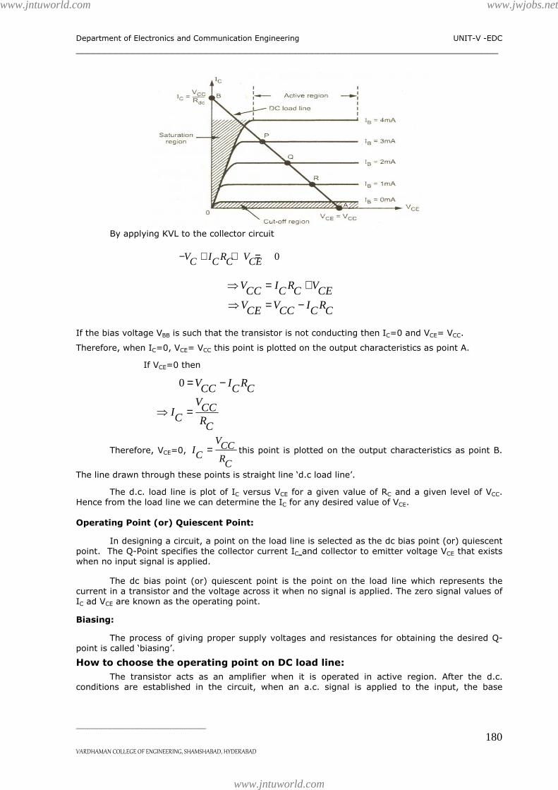
Department of Electronics and Communication Engineering UNIT-V -EDC ___________________________________________________________________________ _____________________________________________________________________________________________________________ VARDHAMAN COLLEGE OF ENGINEERING, SHAMSHABAD, HYDERABAD 179 UNIT-IV TRANSISTOR BIASING Introduction: The basic function transistor is to do amplification. The process of raising the strength of a weak signal without any change in its shape is known as faithful amplification. For faithful amplification, the following three conditions must be satisfied: i) The emitter-base junction should be forward biased, ii) The collector-base junction should be reverse biased. iii) Three should be proper zero signal collector current. The proper flow of zero signal collector current (proper operating point of a transistor) and the maintenance of proper collector-emitter voltage during the passage of signal is known as ‘transistor biasing’. When a transistor is not properly biased, it work inefficiently and produces distortion in the output signal. Hence a transistor is to be biased correctly. A transistor is biased either with the help of battery (or) associating a circuit with the transistor. The latter method is generally employed. The circuit used with the transistor is known as biasing circuit. In order to produce distortion-free output in amplifier circuits, the supply voltages and resistances in the circuit must be suitably chose. These voltages and resistances establish a set of d.c. voltage V CEQ and current I CQ to operate the transistor in the active region. These voltages and currents are called quiescent values which determine the operating point (or) Q-Point for the transistor. The process of giving proper supply voltages and resistances for obtaining the desired Q- Point is called biasing. DC Load Line: Consider common emitter configuration circuit shown in figure below: In transistor circuit analysis generally it is required to determine the value of I C for any desired value of V CE . From the load line method, we can determine the value of I C for any desired value of V CE . The output characteristics of CE configuration is shown in figure below: www.jntuworld.com www.jntuworld.com www.jwjobs.net
Transcript
Department of Electronics and Communication Engineering UNIT-V -EDC
VARDHAMAN COLLEGE OF ENGINEERING, SHAMSHABAD, HYDERABAD 179
UNIT-IV
TRANSISTOR BIASING
Introduction:
The basic function transistor is to do amplification. The process of raising the strength of a weak signal without any change in its shape is known as faithful amplification.
For faithful amplification, the following three conditions must be satisfied:
i) The emitter-base junction should be forward biased, ii) The collector-base junction should be reverse biased. iii) Three should be proper zero signal collector current.
The proper flow of zero signal collector current (proper operating point of a transistor) and the maintenance of proper collector-emitter voltage during the passage of signal is known as ‘transistor biasing’.
When a transistor is not properly biased, it work inefficiently and produces distortion in the output signal. Hence a transistor is to be biased correctly. A transistor is biased either with the help of battery (or) associating a circuit with the transistor. The latter method is generally employed. The circuit used with the transistor is known as biasing circuit.
In order to produce distortion-free output in amplifier circuits, the supply voltages and resistances in the circuit must be suitably chose. These voltages and resistances establish a set of d.c. voltage VCEQ and current ICQ to operate the transistor in the active region. These voltages and currents are called quiescent values which determine the operating point (or) Q-Point for the transistor.
The process of giving proper supply voltages and resistances for obtaining the desired Q-Point is called biasing.
DC Load Line:
Consider common emitter configuration circuit shown in figure below:
In transistor circuit analysis generally it is required to determine the value of IC for any desired value of VCE. From the load line method, we can determine the value of IC for any desired value of VCE. The output characteristics of CE configuration is shown in figure below:
www.jntuworld.com
www.jntuworld.com
www.jwjobs.net
Department of Electronics and Communication Engineering UNIT-V -EDC
VARDHAMAN COLLEGE OF ENGINEERING, SHAMSHABAD, HYDERABAD 180
By applying KVL to the collector circuit
0V I R VC C C CE− + + =
V I R VCC C C CE⇒ = +
V V I RCE CC C C⇒ = −
If the bias voltage VBB is such that the transistor is not conducting then IC=0 and VCE= VCC.
Therefore, when IC=0, VCE= VCC this point is plotted on the output characteristics as point A.
If VCE=0 then
0 V I RCC C C= −
VCCIC RC
⇒ =
Therefore, VCE=0, VCCIC RC
= this point is plotted on the output characteristics as point B.
The line drawn through these points is straight line ‘d.c load line’.
The d.c. load line is plot of IC versus VCE for a given value of RC and a given level of VCC. Hence from the load line we can determine the IC for any desired value of VCE. Operating Point (or) Quiescent Point:
In designing a circuit, a point on the load line is selected as the dc bias point (or) quiescent point. The Q-Point specifies the collector current IC and collector to emitter voltage VCE that exists when no input signal is applied.
The dc bias point (or) quiescent point is the point on the load line which represents the current in a transistor and the voltage across it when no signal is applied. The zero signal values of IC ad VCE are known as the operating point.
Biasing:
The process of giving proper supply voltages and resistances for obtaining the desired Q-point is called ‘biasing’.
How to choose the operating point on DC load line:
The transistor acts as an amplifier when it is operated in active region. After the d.c. conditions are established in the circuit, when an a.c. signal is applied to the input, the base
www.jntuworld.com
www.jntuworld.com
www.jwjobs.net
Department of Electronics and Communication Engineering UNIT-V -EDC
VARDHAMAN COLLEGE OF ENGINEERING, SHAMSHABAD, HYDERABAD 181
current varies according to te amplitude of the signal and causes IC to vary consequently producing an output voltage variation. This can be seen from output characterizes.
Fig. Operating point near saturation region gives clipping at the positive peak.
Consider point A which is very near to the saturation point, even though the base current is varying sinusoidally the output current and output voltage is seen to be clipped at the positive peaks. This results in distortion of the signal.
Consider point B which is very near to the cut-off region. The output signal is now clipped at the negative peak. Hence this two is not a suitable operating point.
Fig. Operating point near cut-off region given clipping at the negative peak.
Consider point C which is the mid point of the DC load line then the output signal will not be distorted.
Fig. Operating point at the centre of active region is most suitable.
www.jntuworld.com
www.jntuworld.com
www.jwjobs.net
Department of Electronics and Communication Engineering UNIT-V -EDC
VARDHAMAN COLLEGE OF ENGINEERING, SHAMSHABAD, HYDERABAD 182
A good amplifier amplifies signals without introducing distortion. Thus always the operating point is chosen as the mid point of the DC load line. Stabilization:
The maintenance of operating point stable is known as ‘Stabilization’.
There are two factors which are responsible for shifting the operating point. They are:
i) The transistor parameters are temperature dependent. ii) When a transistor is replaced by another of same type, there is a wide spread in
the values of transistor parameters.
So, stabilization of the operating point is necessary due to the following reasons:
i) Temperature dependence of IC.
ii) Individual variations and
iii) Thermal runaway. Temperature dependence of IC: The instability of IC is principally caused by the following three sources:
i) The ICO doubles for every 10oC rise in temperature.
ii) Increase of β with increase of temperature.
iii) The VBE decreases about 2.5mV per oC increase in temperature.
Individual variations:
When a transistor is replaced by another transistor of the same type, the values of β and VBE are not exactly the same. Hence the operating point is changed. So it is necessary to stabilize the operating point irrespective of individual variations in transistors parameters. Thermal Runaway:
Depending upon the construction of a transistor, the collector junction can withstand maximum temperature. The range of temperature lies between 60oC to 100oC for ‘Ge’ transistor and 150oC to 225oC for ‘Si’ transistor. If the temperature increases beyond this range then the transistor burns out. The increase in the collector junction temperature is due to thermal runaway.
When a collector current flows in a transistor, it is heated i.e., its temperature increases. If no stabilization is done, the collector leakage current also increases. This further increases the transistor temperature. Consequently, there is a further increase in collector leakage current. The action becomes cumulative and the transistor may ultimately burn out. The self-destruction of an unstabilized transistor is known as thermal runaway.
The following two techniques are used for stabilization.
1) Stabilization techniques:
The technique consists in the use of a resistive biasing circuit which permits such a variation of base current IB as to maintain IC almost constant in spite of ICO, β and VBE.
2) Compensation techniques:
In this technique, temperature sensitive devices such as diodes, thermistors and sensistors etc., are used. Such devices produce compensating voltages and current in such a way that the operating points maintained stable.
Stability factors:
Since there are three variables which are temperature dependent, we can define three stability factors as below:
i) S: The stability factor ‘S’ is defined as the ration of change of collector current IC with respect to the reverse saturation current ICO, keeping β and VBE constant
www.jntuworld.com
www.jntuworld.com
www.jwjobs.net
Department of Electronics and Communication Engineering UNIT-V -EDC
VARDHAMAN COLLEGE OF ENGINEERING, SHAMSHABAD, HYDERABAD 184
1). Fixed bias (or) base resistor method:
A CE amplifier used fixed bias circuit is shown in figure below:
Fig. Fixed bias circuit.
In this method, a high resistance RB is connected between positive terminal of supply VCC and base of the transistor. Here the required zero signal base current flows through RB and is provided by VCC. In figure, the base-emitter junction is forward biased because the base is positive w.r.t. emitter. By a proper selection of RB, the required zero signal base current (and hence IC=βIB) can be made to flow. Circuit Analysis:
Base Circuit:
Consider the base-emitter circuit loop of the above figure.
Writing KVL to the loop, we obtain
0V I R VB B BECC− + + =
V I R VB B BECC⇒ = +
V VBECCIB RB
−⇒ =
But I I IBC CEOβ= +
As ICEO is very small, I IBC β≈
V VBECCIC RB
β−
∴ =
⇒ β, VCC, VBE are constant for a transistor ∴ IC depends on RB.
Choose suitable value of RB to get constant IC in active region.
( )V VBECCRB IC
β−∴ = (or)
VCCRB IC
β= ( )V VBE CC<<Q
Collector Circuit: Consider the collector-emitter circuit loop of the circuit. Writing KVL to the collector circuit, we get
www.jntuworld.com
www.jntuworld.com
www.jwjobs.net
Department of Electronics and Communication Engineering UNIT-V -EDC
VARDHAMAN COLLEGE OF ENGINEERING, SHAMSHABAD, HYDERABAD 187
( )1
V VBECCIB R RB Eβ
−=
+ +
( )20 0.7
3430 51 1040.1IB Aµ−
∴ = =+ ×
2.01I IBC mAβ= =
KVL to collector-emitter loop is
0V I R V I RECC C C CE C− + + + =
( )V V I R RECE CC C C⇒ = − +
3 320 2.01 10 (2 1) 10VCE
−= − × + × =20-6.03 = 13.97V
∴ Operating point is Q (13.97V, 2.01mA)
Advantages of fixed bias circuit:
1. This is a simple circuit which uses very few components.
2. The operating point can be fixed anywhere in the active region of the characteristics by simply changing the values of RB. Thus, it provides maximum flexibility in the design.
Disadvantages of fixed bias circuit:
1. With the rise in temperature the operating point if not stable.
2. When the transistor is replaced by another with different value of β, the operating point with shift i.e., the stabilization of operating point is very poor in fixed bias circuit.
Because of these disadvantages, fixed bias circuit required some modifications. In the modified circuit, RB is connected between collector and base. Hence the circuit is called ‘collector to base’ bias circuit.
2). Collector to Base bias (or) Biasing with feedback resistor: A CE amplifier using collector to base bias circuit is shown in the figure. In this method, the biasing resistor is connected between the collector and the base of the transistor.
Fig. Collector–to–Base bias circuit.
Circuit Analysis:
Base Circuit:
www.jntuworld.com
www.jntuworld.com
www.jwjobs.net
Department of Electronics and Communication Engineering UNIT-V -EDC
VARDHAMAN COLLEGE OF ENGINEERING, SHAMSHABAD, HYDERABAD 189
We have ( )V V I RBECC C CIC R RBC
β − −=
+
Differentiating the above equation w.r.t. IC,
We get 1RV CBE
R R I R RB BC C C
β β∂
= − −+ ∂ +
1R VC BE
R R R R IB BC C C
ββ∂
+ = −+ + ∂
R R R VBC C BE
R R R R IB BC C C
β β+ + ∂= −
+ + ∂
( )'
1S
R RB C
ββ⇒ = −
+ + ………………….. (5)
Stability factor S’’:
We have ( )V V I RBECC C CIC R RBC
β − −=
+
Differentiating the above equation w.r.t. β,
We get I V V R IBEC CC C CICR R R RB BC C
ββ β
∂ − ∂= − +
∂ + + ∂
1I R V V I RBEC C CC C C
R R R RB BC Cβ
β
∂ − −⇒ + =
∂ + +
( )1IC R R V V I RB BEC CC C Cββ
∂⇒ + = − −
∂
( )
''1
V V I RBECC C CSR RB Cβ
− −⇒ =
+ +
( )
( )''
1
I R RBC CSR RB Cβ
+⇒ =
+ + ……………… (6)
Problems:
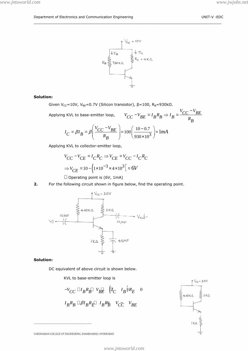
3. An N-P-N transistor with β=50 is used in a CE circuit with VCC=10V, RC=2kΩ. The bias is obtained by connecting a 100kΩ resistance from collector to base. Assume VBE=0.7V. Find
i) the quiescent point and ii) Stability factor ‘S’
Solution:
i) Applying KVL to the base circuit,
www.jntuworld.com
www.jntuworld.com
www.jwjobs.net
Department of Electronics and Communication Engineering UNIT-V -EDC
VARDHAMAN COLLEGE OF ENGINEERING, SHAMSHABAD, HYDERABAD 190
( )V I I R I R VB B B BECC C C+ + +=
( )V I R R I R VB B BECC C C C⇒ = + + +
V V I RBECC C CIB R RBC
− −∴ =
+
( )V V I RBECC C CIC R RBC
β − −∴ =
+
( )350 10 0.7 2 10
3102 10
ICIC
−− − ×∴ =
× 2.3CI mA⇒ =
Applying KVL to the collector circuit,
( )V I I R VBCC C C CE+ += ( )V V I I RBCE CC C C∴ += −
( )6 3 310 46 10 2.3 10 2 10− −= − × + × × ×
5.308V VCE⇒ = ∴The quiescent point is (5.308V, 2.3mA)
ii) Stability factor, S:
1
1
SRC
R RBC
β
β
+=
++
51
25.75320 10
1 50 3102 10
S
⇒ = =×+×
4. A transistor with β=45 is used with collector to base resistor RB biasing with quiescent value of 5V for VCE. If VCC=24V, RC=10kΩ, RE=270Ω, find the value of RB.
Solution:
Applying KVL to collector and emitter loop, we have
0V I R V I RE ECC C C CE− − − =
( )V V I R I I RB ECC CE C C C⇒ − = + +
( )1V V R R IE BCC CE Cβ β⇒ − = + +
( )1
V VBECCIB R RECβ β
−⇒ =
+ +
24 5
45 10 50 0.27
−=
× + ×
=0.041 mA
Further, 0V I R I R V I RB B BE E ECC C C− − − − =
( )1V V R I I R R IBE B B B E BCC C β β⇒ − = + + + `
VARDHAMAN COLLEGE OF ENGINEERING, SHAMSHABAD, HYDERABAD 191
105.87BR K∴ = Ω
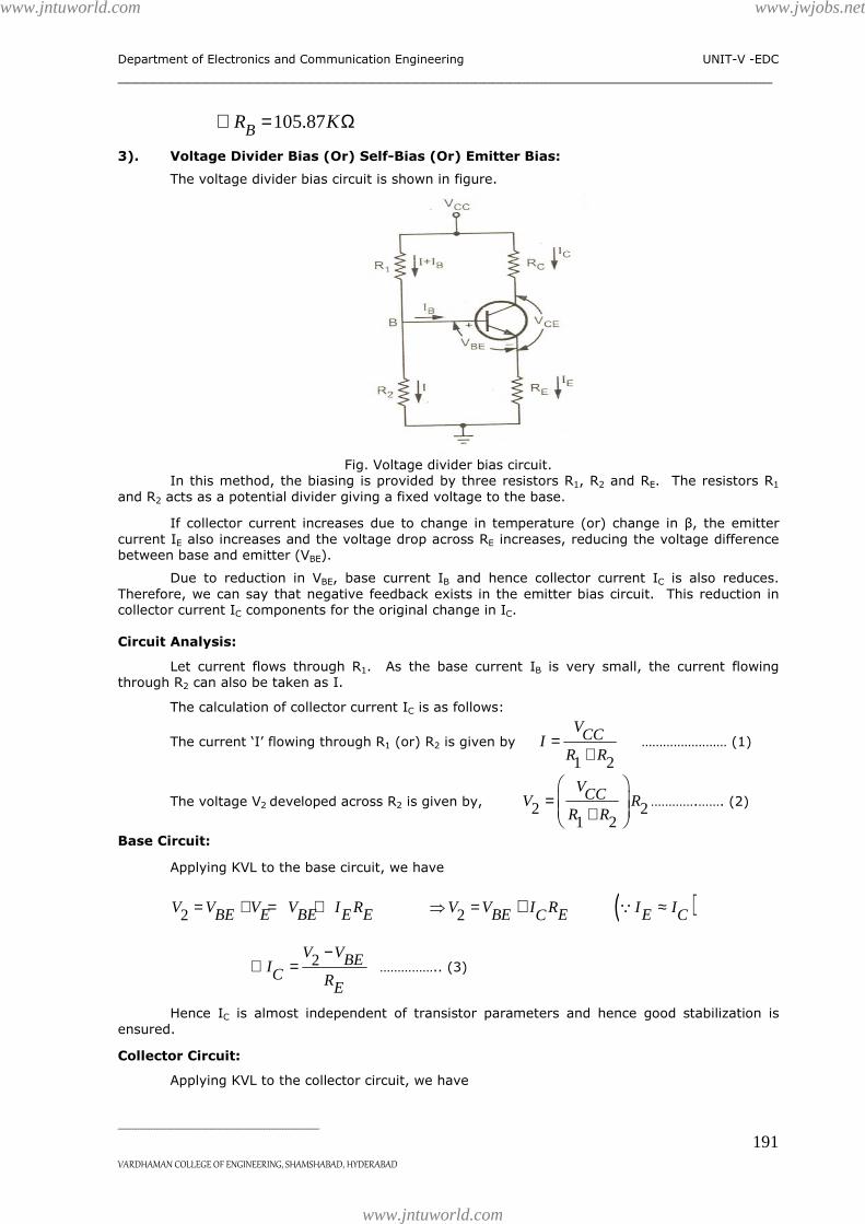
3). Voltage Divider Bias (Or) Self-Bias (Or) Emitter Bias:
The voltage divider bias circuit is shown in figure.
Fig. Voltage divider bias circuit.
In this method, the biasing is provided by three resistors R1, R2 and RE. The resistors R1 and R2 acts as a potential divider giving a fixed voltage to the base.
If collector current increases due to change in temperature (or) change in β, the emitter current IE also increases and the voltage drop across RE increases, reducing the voltage difference between base and emitter (VBE).
Due to reduction in VBE, base current IB and hence collector current IC is also reduces. Therefore, we can say that negative feedback exists in the emitter bias circuit. This reduction in collector current IC components for the original change in IC. Circuit Analysis:
Let current flows through R1. As the base current IB is very small, the current flowing through R2 can also be taken as I.
The calculation of collector current IC is as follows:
The current ‘I’ flowing through R1 (or) R2 is given by
1 2
VCCIR R
=+
…………………… (1)
The voltage V2 developed across R2 is given by, 2 21 2
VCCV RR R
=+
………….……. (2)
Base Circuit:
Applying KVL to the base circuit, we have
2V V V V I RBE E BE E E= + = + 2V V I RBE EC⇒ = + ( )I IE C≈Q
2V VBEIC RE
−∴ = …………….. (3)
Hence IC is almost independent of transistor parameters and hence good stabilization is ensured.
Collector Circuit:
Applying KVL to the collector circuit, we have
www.jntuworld.com
www.jntuworld.com
www.jwjobs.net
Department of Electronics and Communication Engineering UNIT-V -EDC
VARDHAMAN COLLEGE OF ENGINEERING, SHAMSHABAD, HYDERABAD 193
………….…….. (8) From equation (8), we have
V VCC CEIC R REC
−∴ =
+
Substituting this value of IC in equation (7), we have
V VCC CEV I R V R IB BE E BTh Th R REC
−= + + +
+
(or) R V R VE ECC CEV I R V R IB BE E BTh Th R R R RE EC C
= + + + −+ +
From equation (9) we can calculate the value of collector voltage VCE for each value of IB.
Stability factor (S):
For determining stability factor ‘S’ for voltage divider bias, consider the Thevenin’s equivalent circuit. Hence, Thevenin’s equivalent voltage VTh is given by
2
1 2
RV VCCTh R R
=+
and the R1 and R2 are replaced by RB which is the parallel combination of R1 and R2.
1 2
1 2
R RRB R R
∴ =+
Applying KVL to the base circuit, we get ( )V I R V I I RB B BE B ECTh = + + +
Differentiating w.r.t. IC and considering VBE to be independent of IC we get,
( )0I IB BR R RB E EI IC C
∂ ∂= × + +
∂ ∂
( )IB R R RE B EIC
∂∴ + = −
∂
I RB EI R RE BC
∂ −∴ =
∂ +
We have already seen the generalized expression for stability factor ‘S’ given by
1
1
SIBIC
β
β
+=
∂−
∂
Substituting value of IBIC
∂
∂in the above equation, we get
www.jntuworld.com
www.jntuworld.com
www.jwjobs.net
Department of Electronics and Communication Engineering UNIT-V -EDC
VARDHAMAN COLLEGE OF ENGINEERING, SHAMSHABAD, HYDERABAD 197
32 10312 2 10 101 5003 100R
−×−⇒ = × × + × ×
5.4953R k⇒ = Ω
From Base circuit, 22
1 2
RV VCCR R
=+
310 10152 310 101
VR
−×⇒ = ×−+ ×
But, ( )0.6 0.6 12 4 4V V V I R I RBE E E Bβ= + = + = + +
32 100.6 101 500 1.612 100
V V−×
⇒ = + × × =
31 101.61 15310 101R
−×∴ = ×−+ ×
3 310 10 93.17 101R −⇒ + × = ×
83.171R k⇒ = Ω
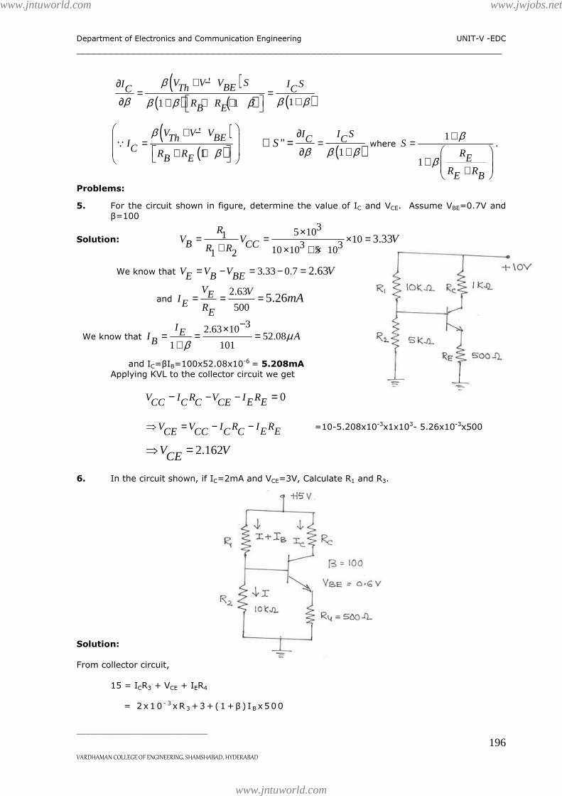
7. For the circuit shown below, calculate VE, IE, IC and VC. Assume VBE=0.7V.
Solution:
From Base circuit,
4 0.7V V VBE E E= + = +
3.3V VE⇒ =
3.3I RE E =
3.31
33.3 10I mAE⇒ = =
×
But IE=IB+IC = (1+β)IB Assume β=100,
10.0099
101
mAI mAB⇒ = =
IC=βIB = 100x0.0099mA = 0.99mA
From Collector circuit,
10 100 0.99 4.7 5.347V I R mA KC C C V= − = − × Ω =
Bias Compensation Techniques: The biasing circuits provide stability of operating point in case variations in the transistor parameters such as ICO, VBE and β.
www.jntuworld.com
www.jntuworld.com
www.jwjobs.net
Department of Electronics and Communication Engineering UNIT-V -EDC
VARDHAMAN COLLEGE OF ENGINEERING, SHAMSHABAD, HYDERABAD 198
The stabilization techniques refer to the use of resistive biasing circuits which permit IB to vary so as to keep IC relatively constant. On the other hand, compensation techniques refer to the use of temperature sensitive devices such as diodes, transistors, thermistors, sensistors etc., to compensate for the variation in currents. Sometimes for excellent bias and thermal stabilization, both stabilization as well as compensation techniques are used. The following are some compensation techniques:
1) Diode compensation for instability due to VBE variation. 2) Diode compensation for instability due to ICO variation. 3) Thermistor compensation. 4) Sensistor compensation.
1) Diode compensation for instability due to VBE variation:
For germanium transistor, changes in ICO with temperature contribute more serious problem than for silicon transistor. On the other hand, in a silicon transistor, the changes of VBE with temperature possesses significantly to the changes in IC. A diode may be used as compensation element for variation in VBE (or) ICO. The figure below shows the circuit of self bias stabilization technique with a diode compensation for VBE. The Thevenin’s equivalent circuit is shown in figure. Fig. Self bias with stabilization and compensation Fig. Thevenin’s equivalent circuit The diode D used here is of the same material and type as the transistor. Hence the voltage VD across the diode has same temperature coefficient (-2.5mV/oC) as VBE of the transistor. The diode D is forward biased by the source VDD and resistor RD. Applying KVL to the base circuit, we get
0V I R V I R VB BE E E DTh Th− + + + − =
( )V V V I R R I IBE D B E E CTh Th⇒ − + = + + …………………. (1)
But ( )1I I IBC COβ β= + + ………………... (2)
From equation (1), we get
www.jntuworld.com
www.jntuworld.com
www.jwjobs.net
Department of Electronics and Communication Engineering UNIT-V -EDC
VARDHAMAN COLLEGE OF ENGINEERING, SHAMSHABAD, HYDERABAD 199
( )V V V R I R R IBE D E E BCTh Th− + = + +
Substituting the value of IB from equation (2), we get
( ) ( )1I IC COV V V R I R RBE D E ECTh Th
β
β
− +− + = + +
( ) ( ) ( ) ( )1V V V R I R R I I R RBE D E E EC C COTh Th Thβ β β⇒ − + = + + − + +
( ) ( ) ( ) ( )( )1 1V V V I R R I R RBE D E ECO CTh Th Thβ β β⇒ − + = + + = + +
( ) ( ) ( )( )
1
1
V V V I R RBE D ECOTh ThIC R RETh
β β
β
− + = + +⇒ =
+ + …………… (3)
Since variation in VBE with temperature is the same as the variation in VD with temperature,
hence the quantity (VBE-VD) remains constant in equation (3). So the current IC remains constant in spite of the variation in VBE.
2) Diode compensation for instability due to ICO variation: Consider the transistor amplifier circuit with diode D used for compensation of variation in ICO. The diode D and the transistor are of the same type and same material.
In this circuit diode is kept in reverse biased condition. The reverse saturation current IO of the diode will increase with temperature at the same as the transistor collector saturation current ICO.
From figure V V VBECC CCI
R R
−= ≈ = constant.
The diode D is reverse biased by VBE. So the current through D is the reverse saturation current IO. Now base current IB=I-IO
But ( )1I I IBC COβ β= + +
www.jntuworld.com
www.jntuworld.com
www.jwjobs.net
Department of Electronics and Communication Engineering UNIT-V -EDC
VARDHAMAN COLLEGE OF ENGINEERING, SHAMSHABAD, HYDERABAD 200
( ) ( )1I I I IC O COβ β⇒ = − + +
If β>>1, I I I IC O COβ β β≈ − +
In the above expression, I is almost constant and if IO of diode D and ICO of transistor track each other over the operating temperature range, then IC remains constant.
3) Thermistor Compensation:
This method of transistor compensation uses temperature sensitive resistive elements, thermistor rather than diodes (or) transistors: It has a negative temperature coefficient, its resistance decreases exponentially with increasing temperature as shown in the figure.
Slope of this curve RTT
∂=
∂
RTT
∂
∂ is the temperature coefficient for thermistor, and
the slope is negative. So we can say that thermistor has negative temperature coefficient of resistance.
As shown in figure, R2 is replaced by thermistor RT in self bias circuit.
Fig. Thermistor compensation technique.
With increase in temperature, RT decreases. Hence voltage drop across it also decreases. This voltage drop is nothing but the voltage at the base with respect to ground. Hence, VBE decreases which reduces IB. This behavior will tend to offset the increase in collector current with temperature.
We know, ( )1I I IBC COβ β= + +
www.jntuworld.com
www.jntuworld.com
www.jwjobs.net
Department of Electronics and Communication Engineering UNIT-V -EDC
VARDHAMAN COLLEGE OF ENGINEERING, SHAMSHABAD, HYDERABAD 201
In this equation, there is increase in ICBO and decreases in IB which keeps IC almost constant. Consider another thermistor compensation technique shown in figure. Here, thermistor is connected between emitter and VCC to minimize the increase in collector current due to change in ICO, VBE (or) β with temperature.
Fig. Thermistor compensation technique.
IC increase with temperature and RT decreases with increase in temperature. Therefore, current flowing through RE increases, which increases the voltage drop across it. Emitter to Base junction is forward biased. But due to increase in voltage drop across RE, emitter is made more positive, which reduces the forward bias voltage VBE. Hence, base current reduces.
IC is given by, ( )1I I IBC COβ β= + +
As ICBO increases with temperature, IB decreases and hence IC remain fairly constant. 4) Sensistor Compensation:
This method of transistor compensation uses sensistor, which is temperature sensitive resistive element. Sensistor has a positive temperature coefficient, i.e., its resistance increases exponentially with increasing temperature.
Slope of this curve RTT
∂=
∂
RTT
∂
∂ is the temperature coefficient for sensistor, and the
slope is positive. So we can say that sensistor has positive temperature coefficient of resistance.
As shown in figure R1 is replaced by sensistor RT in self bias circuit.
As temperature increases, RT increases which decreases the current flowing through it. Hence current through R2 decreases which reduces the voltage drop across it.
www.jntuworld.com
www.jntuworld.com
www.jwjobs.net
Department of Electronics and Communication Engineering UNIT-V -EDC
VARDHAMAN COLLEGE OF ENGINEERING, SHAMSHABAD, HYDERABAD 202
Fig. Sensistor compensation technique.
As voltage drop across R2 decreases, IB decreases. It means, when ICBO increases with increase in temperature, IB reduces due to variation in VBE, maintaining IC fairly constant.
Thermal Runaway: The collector current for the CE circuit is given by
( )1I I IBC COβ β= + +
The three variables in the equation, β, IB and ICO increase with rise in temperature. In particular, the reverse saturation current (or) leakage current ICO changes greatly with temperature. Specifically, it doubles for every 10oC rise in temperature.
The collector current IC causes the collector-base junction temperature to rise which, in turn, increase ICO, as a result IC increase still further, which will further rise the temperature at the collector-base junction. This process is cumulative and it is referred to as self heating.
The excess heat produced at the collector-base junction may even burn and destroy the transistor. This situation is called “Thermal Runaway” of the transistor. Thermal Resistance:
Transistor is a temperature dependent device.
In order to keep the temperature within the limits, the heat generated must be dissipated to the surroundings.
Most of the heat within the transistor is produced at the collector junction.
If the temperature exceeds the permissible limit, the junction is destroyed.
For Silicon transistor, the temperature is in the range 150oC to 225oC.
For Germanium, it is between 60oC to 100oC.
Let TAoC be the ambient temperature i.e., the temperature of surroundings air around
transistor and TjoC, the temperature of collector-base junction of the transistor.
Let PD be the power in watt dissipated at the collector junction.
www.jntuworld.com
www.jntuworld.com
www.jwjobs.net
Department of Electronics and Communication Engineering UNIT-V -EDC
VARDHAMAN COLLEGE OF ENGINEERING, SHAMSHABAD, HYDERABAD 203
The steady state temperature rise at the collector junction is proportional to the power dissipated at the junction. It is given by
T T T Pj DA θ∂ = − = Where θ = constant of proportionality
The θ, which is constant of proportionality, is referred to as thermal resistance.
T Tj A
PDθ
−=
The unit of θ, the thermal resistance, is oC/watt.
The typical values of θ for various transistors vary from 0.2oC/watt for a high power transistor to 1000 oC/watt for a low power transistor.
Heat Sink:
As power transistors handle large currents, they always heat up during operation.
The metal sheet that helps to dissipate the additional heat from the transistor is known as heat sink. The heat sink avoids the undesirable thermal effect such as thermal runaway.
The ability of heat sink depends on the material used, volume, area, shape, constant between case and sink and movement of air around the sink.
The condition for Thermal Stability:
As we know, the thermal runaway may even burn and destroy the transistor, it is necessary to avoid thermal runaway.
The required condition to avoid thermal runaway is that the rate at which heat is released at the collector junction must not exceed the rate at which the heat can be dissipated. It is given
by P PC DT Tj j
∂ ∂<
∂ ∂ ………………(1)
But we know, from thermal resistance
T T Pj DA θ− = …………….. (2)
Differentiating equation (2) w.r.t. Tj we get
1PDTj
θ∂
=∂
1PD
Tj θ
∂⇒ =
∂ ………………. (3)
Substituting equation (3) in equation (1), we get
1PD
Tj θ∂
∴ <∂
……………… (4)
This condition must be satisfied to prevent thermal runaway.
By proper design of biasing circuit it is possible to ensure that the transistor cannot runaway below a specified ambient temperature (or) even under any condition.
Let us consider voltage divider bias circuit for the analysis.
www.jntuworld.com
www.jntuworld.com
www.jwjobs.net
Department of Electronics and Communication Engineering UNIT-V -EDC
VARDHAMAN COLLEGE OF ENGINEERING, SHAMSHABAD, HYDERABAD 204
Fig. Voltage divider bias circuit.
From fig., PC = heat generated at the collector junction. = DC power input to the circuit – the power lost as I2R in RC and RE.
If we consider I IEC ≅ we get
( )2P V I I R REC CC C C C= − + ……………….. (6)
Differentiating equation (6) w.r.t IC we get
( )2PC V I R RECC C CIC
∂= − +
∂ ……………….. (7)
From equation (4)
1.
P IC CI T jC θ
∂ ∂<
∂ ∂ ……………….. (8)
In the above equation ICTj
∂
∂can be written as
' "I I VC CO BES S ST T T Tj j j j
β∂ ∂ ∂ ∂= + +
∂ ∂ ∂ ∂ ………………. (9)
Since junction temperature affects collector current by affecting ICO, VBE, and β. But as we are doing analysis for thermal runaway the affect of ICO dominates. Thus we can write
I IC COST Tj j
∂ ∂=
∂ ∂ …………………….. (10)
As the reverse saturation current for both Silicon and Germanium increases about 7 percent per oC, we can write
www.jntuworld.com
www.jntuworld.com
www.jwjobs.net
Department of Electronics and Communication Engineering UNIT-V -EDC
VARDHAMAN COLLEGE OF ENGINEERING, SHAMSHABAD, HYDERABAD 205
0.07ICO ICOTj
∂=
∂ ……………………. (11)
Substituting equation (11) in equation (10), we get
0.07IC S ICOTj
∂= ×
∂ ……………………. (12)
Substituting equations (7) and (12) in equation (8), we get
( ) ( )( ) 12 0.07V I R R S IECC C C CO θ
− + <
………………….. (13)
As S, ICO and θ are positive; we see that the inequality in equation (13) is always satisfied provided that the quantity in the square bracket is negative.
( )2V I R RECC C C∴ < +
( )2
VCC I R REC C⇒ < + ……………….. (14)
Applying KVL to the collector circuit of voltage divider bias circuit we get,
( )V V I R RECE CC C C= − + ( )I IEC ≅Q
( )I R R V VEC C CC CE∴ + = −
Substituting the value of ( )I R REC C + in equation (14), we get