FEATURES: • Xilinx XC3S200A-4FTG256C FPGA utilized on the DLP-HS-FPGA • Xilinx XC3S400A-4FTG256C FPGA utilized on the DLP-HS-FPGA2 • Micron 32M x 8 DDR2 SDRAM Memory • Built-In Configuration Loader; Writes the Bit File Directly to SPI Flash via High-Speed USB 2.0
Interface • 63 User I/O Channels: 24 Differential Pairs and 8 Global Clocks • 66 MHz Oscillator • 133 MHz DDR2 Interface Reference Design Provided • USB Port Powered or 5V External Power Barrel Jack • USB 1.1 and 2.0 Compatible Interface • Small Footprint: 3.0 x 1.2-Inch PCB and Standard 50-Pin, 0.9-Inch DIP Interface
APPLICATIONS: • Rapid Prototyping • Educational Tool • Industrial/Process Control • Data Acquisition/Processing • Embedded Processor 1.0 INTRODUCTION The DLP-HS-FPGA module is a low-cost, compact prototyping tool that can be used for rapid proof of concept or within educational environments. The module is based on the Xilinx Spartan™ 3A and Future Technology Devices International’s FT2232H Dual-Channel High-Speed USB IC. The DLP-HS-FPGA provides both the beginner as well as the experienced engineer with a rapid path to developing FPGA-based designs. When combined with the free ISE™ WebPACK™ tools from Xilinx, this module is more than sufficient for creating anything from basic logical functions to a highly complex system controller. As a bonus feature, one channel of the dual-channel USB interface is used to load user bit files directly to the SPI Flash—no external programmer is required. This represents a savings of as much as $200 in that no additional programming cable is required for configuring the FPGA. All that is needed to load bit files to the DLP-HS-FPGA is a Windows software utility (free with purchase), a Windows PC and a USB cable. The module can also be programmed from within the Xilinx ISE tool environment using a Xilinx programming cable (purchased separately). The DLP-HS-FPGA is fully compatible with the free ISE™ WebPACK™ tools from Xilinx. ISE WebPACK offers the ideal development environment for FPGA designs with HDL synthesis and simulation, implementation, device fitting and JTAG programming. The DLP-HS-FPGA has on-board voltage regulators that generate all required power supply voltages from a single 5-volt source. Power for the module can be taken from either the host USB port or from a user-supplied, external 5-volt power supply via an onboard standard barrel connector.
Connection to user electronics is made via a 50-pin, 0.9-inch wide, industry-standard 0.025-square inch post DIP header on the bottom of the board and a 26-pin, 0.05-inch wide top side 2x13 header. The bottom side 50-pin header provides access to 41 of the FPGA user input/output pins. The top side header provides access to 22 of the FPGA user input/output pins. The bottom side header mates with a user-supplied, standard, 50-pin, 0.9-inch spaced DIP socket. The top side header mates with a
user-supplied, 0.05-inch spaced, 2x13 connector such as the FFSD-13-D-xx.xx-01 (xx.xx = cable length) ribbon cable assembly from Samtec.
DIP Socket
Ribbon Cable
Other on-board features include a 32M x 8 DDR2 SDRAM memory IC for user projects and both JTAG and SPI Flash interface ports for connection to Xilinx programming tools. 2.0 REFERENCE DESIGN A 10,000-line reference design is available for the Spartan™ 3A FPGA on the DLP-HS-FPGA to those who purchase the module. The design was written in VHDL and built using the free Xilinx ISE™ WebPACK™ tools. The reference design consists of the following blocks:
It contains a USB Interface Block, a User I/0 Block, a DDR2 SDRAM interface, a Heartbeat Pulse Generator and a Clock Generator. The SPI Flash is used to store the design’s FPGA configuration file. The USB interface captures, interprets and returns command and data information sent from the host PC through the FTDI USB interface to the FPGA. Commands include Ping, Return Status, Loopback Data, Set a User I/O Pin High or Low, Read a User I/O Pin, Initialize the DDR2 SDRAM Memory and Read or Write the DDR2 SDRAM Memory. (Section 11 explains these in detail.)
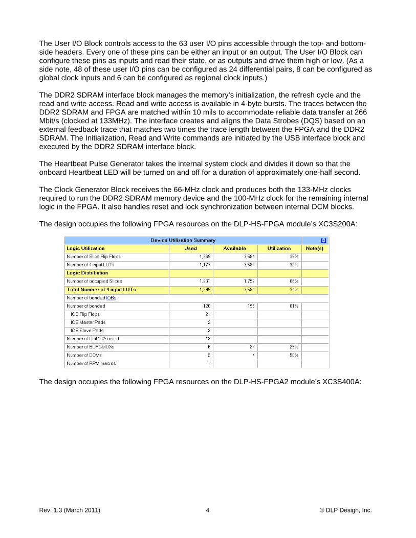
The User I/O Block controls access to the 63 user I/O pins accessible through the top- and bottom- side headers. Every one of these pins can be either an input or an output. The User I/O Block can configure these pins as inputs and read their state, or as outputs and drive them high or low. (As a side note, 48 of these user I/O pins can be configured as 24 differential pairs, 8 can be configured as global clock inputs and 6 can be configured as regional clock inputs.) The DDR2 SDRAM interface block manages the memory’s initialization, the refresh cycle and the read and write access. Read and write access is available in 4-byte bursts. The traces between the DDR2 SDRAM and FPGA are matched within 10 mils to accommodate reliable data transfer at 266 Mbit/s (clocked at 133MHz). The interface creates and aligns the Data Strobes (DQS) based on an external feedback trace that matches two times the trace length between the FPGA and the DDR2 SDRAM. The Initialization, Read and Write commands are initiated by the USB interface block and executed by the DDR2 SDRAM interface block. The Heartbeat Pulse Generator takes the internal system clock and divides it down so that the onboard Heartbeat LED will be turned on and off for a duration of approximately one-half second. The Clock Generator Block receives the 66-MHz clock and produces both the 133-MHz clocks required to run the DDR2 SDRAM memory device and the 100-MHz clock for the remaining internal logic in the FPGA. It also handles reset and lock synchronization between internal DCM blocks. The design occupies the following FPGA resources on the DLP-HS-FPGA module’s XC3S200A:
The design occupies the following FPGA resources on the DLP-HS-FPGA2 module’s XC3S400A:
More reference designs are planned. Please contact DLP Design with any specific requests. 3.0 FPGA SPECIFICATIONS
The FPGA device used on the DLP-HS-FPGA is the Xilinx Spartan™ 3A: XC3S200A-4FTG256 • Part Number: XC3S200A-4FTG256C • System Gates: 200,000 • Equivalent Logic Cells: 4,032 • CLB Array:
Rows: 32 Columns: 16 Total CLB’s: 448 Total Slices: 1,792 Total Flip Flops: 3,584 Total 4-Input LUT’s: 3,584
The FPGA device used on the DLP-HS-FPGA2 is the Xilinx Spartan™ 3A: XC3S400A-4FTG256 • Part Number: XC3S400A-4FTG256C • System Gates: 400,000 • Equivalent Logic Cells: 8,064 • CLB Array:
Rows: 40 Columns: 24 Total CLB’s: 896 Total Slices: 3,584 Total Flip Flops: 7,168 Total 4-Input LUT’s: 7,168
• Distributed RAM Bits: 56K • Block RAM Bits: 360K • Dedicated Multipliers: 20 • DCM’s: 4 4.0 ABSOLUTE MAXIMUM RATINGS Stresses above those listed here may cause permanent damage to the DLP-HS-FPGA: Operating Temperature: 0-70°C Voltage on Digital Inputs with Respect to Ground: -0.5V to +4.1 V Sink/Source Current on Any I/O: 24 mA (using LVTTL as the FPGA I/O standard) 5.0 WARNINGS • Unplug from the host PC and power adapter before connecting to I/O on the DLP-HS-FPGA.
• Isolate the bottom of the board from all conductive surfaces.
• Observe static precautions to prevent damage to the DLP-HS-FPGA module. 6.0 BITLOADAPP SOFTWARE Windows software is provided for use with the DLP-HS-FPGA that will load an FPGA configuration (*.bit) file directly to the SPI Flash device via the USB interface. This application (illustrated below) will allow the user to erase the Flash, verify the erasure and then program and verify the Flash:
7.0 JTAG INTERFACE The easiest way to load an FPGA configuration (*.bit) file to the FPGA is to run the BitLoadApp software then select and program a file from the local hard drive directly to the SPI Flash. Once written to the SPI Flash, the configuration will load to the FPGA and execute. Alternatively, a traditional JTAG header location is provided on the DLP-HS-FPGA giving the user access to the specific pins required by the development tools. (Refer to the schematic contained within this datasheet for details.) 8.0 EEPROM SETUP / MPROG The DLP-HS-FPGA has a dual-channel USB interface to the host PC. Channel A is used exclusively to load an FPGA configuration (*.bit) file to the SPI Flash. This configuration data is automatically transferred to the FPGA when power is applied to the module or when the PROG Pin is driven low and then released by the application software. Channel B is used for communication between the FPGA and host PC at run time. A 93LC56B EEPROM connected to the USB interface IC is used to store the setup for the two channels. The parameters stored in the EEPROM include the Vendor ID (VID), Product ID (PID), Serial Number, Description String, driver selection (VCP or D2XX) and port type (UART serial or FIFO parallel). As mentioned above, Channel A is used exclusively for loading the FPGA’s configuration to the SPI Flash, and Channel B is used for communication between the host PC and the DLP-HS-FPGA. As such, the D2XX drivers and 245 FIFO mode must be selected in the EEPROM for Channel A. Channel B must use the 245 FIFO mode, but it can use either the VCP or D2XX drivers. The VCP drivers make the DLP-HS-FPGA appear as an RS232 port to the host application. The D2XX drivers provide faster throughput, but require working with a *.lib or *.dll library in the host application. The operational modes and other EEPROM selections are written to the EEPROM using the MPROG utility. This utility and its manual are available for download from the bottom of the page at www.dlpdesign.com.
9.0 TEST BIT FILE A test file is provided as a download from the DLP Design website that provides rudimentary access to the I/O features of the DLP-HS-FPGA. The following features are provided: • Ping
• Read the High/Low State of the Input-Only Pins
• Drive I/O Pins High/Low or Read their High/Low State
• Simple Loopback on Channel B
• 4 Byte Read/Write Access of Row, Column, and Bank Address in the DDR2 SDRAM This bit file is available from the DLP-HS-FPGA’s download page. The command structure that supports these features is explained in Section 11.
10.0 USB DRIVERS USB drivers for the following operating systems are available for download from the DLP Design website at www.dlpdesign.com:
OPERATING SYSTEM SUPPORT Windows 7 32-bit Windows 7 64-bit
Windows Vista, Vista x64 Mac OSX Windows XP, XP x64 Mac OS9
Windows Server 2008, x64 Mac OS8 Windows Server 2003, x64 Linux
Windows 2000 Windows CE 4.2 – 6.0 Notes: 1. The bit file load utility only runs on the Windows platforms. 2. The bit file load utility requires the use of USB channel A, and channel A is dedicated to this
function. 3. If you are utilizing the dual-mode drivers from FTDI (CDM2.x.x) and you want to use the Virtual COM Port (VCP) drivers, then it may be necessary to disable the D2XX drivers first via Device Manager. To do so, right click on the entry under USB Controllers that appears when the
DLP-HS-FPGA is connected, select Properties, select the Advanced tab, check the option for “Load VCP” and click OK. Then unplug and replug the DLP-HS-FPGA, and a COM port should appear in Device Manager under Ports (COM & LPT).
11.0 USING THE DLP-HS-FPGA Select a power source via Header Pins 23 and 24, and connect the DLP-HS-FPGA to the PC to initiate the loading of USB drivers. The easiest way to do this is to connect Pins 23 and 24 to each other. This will result in operational power being taken from the host PC. Once the drivers are loaded, the DLP-HS-FPGA is ready for use.
Simply connect the DLP-HS-FPGA to the PC to initiate the loading of USB drivers. Once the USB drivers are loaded, the DLP-HS-FPGA is ready for use. All commands are issued as multi-byte command packets consisting of at least two bytes.
You can either utilize the Test Application available from http://www.dlpdesign.com/test.shtml with the DLP-HS-FPGA (as described in Section 12), or you can write your own program in your language of choice. If you are using the VCP drivers, begin by opening the COM port, and send multi-byte commands as shown in Table 1 below. There is no need to set the baud rate because the DLP-HS-FPGA uses a parallel interface between the USB IC and the FPGA. (The Ping Command can be used to locate the correct COM port used for communicating with the DLP-HS-FPGA, or you can look in Device Manager to see which port was assigned by Windows.) If you are using the D2XX drivers as with the Test Application, no COM port selection is necessary.
TABLE 1 Command Packets
Command Packet
Description
Byte
Hex Value
Return/Comments
Ping Issues Ping 0 0x00 Ping Command - 0x56 will be returned indicating that the DLP-HS-FPGA is found on the selected port.
0x00 = Board ID (0x11 = Production PCB) 0x01 = FPGA Type ID : 0x3A = XC3S200A 0x4A = XC3S400A 0x02 = Design Version ID 1 (Design Month) 0x03 = Design Version ID 2 (Design Day) 0x04 = Design Version ID 3 (Design Year) 0x05 = Design Version ID 4 (Design Version) 0x06 = DDR2 Status: 0x00 = Not Initialized 0x01 = Initialized
Loopback Returns the data byte received
0 0x20 Loopback Command 1 0xnn The byte sent to the DLP-HS-FPGA (0xnn) will be
returned back. Loopback
Compliment Returns the compliment of data byte received
0 0x21 Loopback Compliment Command 1 0xnn The byte sent to the DLP-HS-FPGA (0xnn) will be
complimented and returned back.
Read Pin Reads the state of one of the user I/O pins
0 0x30 Read Pin Command 1 0x00
– 0x3E
The user I/O pin numbers are described in Table 2. User I/O pin 0xnn is read and returns: 0x00 = User I/O pin 0xnn is low 0x01 = User I/O pin 0xnn is high
The user I/O pin numbers are described in Table 2. User I/O pin 0xnn is cleared. The specified user I/O number is returned.
Set Pin Forces the selected user I/O pin high
0 0x41 Set Pin Command 1 0x00
– 0x3E
The user I/O pin numbers are described in Table 2. User I/O pin 0xnn is set. The specified user I/O number is returned.
Initialize Memory
Initializes DDR2 SDRAM
0 0x70 The Initialize Memory Command configures the DDR2 SDRAM for access by the FPGA. The memory cannot be accessed without being initialized.
Important Note on DDR2 SDRAM Data Access: DDR2 SDRAM data accesses using the reference design on the DLP-HS-FPGA module are always performed 4 bytes at a time due to the fact that the device is configured for a burst length of four. What this means is that column address Bits 0 and 1 only change the order of the read or write bytes; they still refer to the same 4 bytes. Therefore, to increment the DDR2 SDRAM address for consecutive memory locations, the column address must be incremented by 4. Incrementing the column address by anything less than 4 simply changes the order in which the 4 bytes specified by column address 9:3 are written to the memory or returned to the user. For example, a write to a column starting address of 0 will write to column locations 0, 1, 2 and 3. But if the user then writes to column address 1, they will actually be writing to column locations 1, 2, 3 and 0, which will overwrite the previous write operation. More details on how the DDR2 SDRAM column bits 1 and 0 function can be found in Figure 4 and Table 40 of the Micron™ MT47H32M8 datasheet. For details on how the bank, row and column bits are sent via USB to the memory, refer to the commands below:
Memory Read
Reads 4 bytes from the DDR SDRAM
0 0x8n Reads 4 bytes from the DDR2 SDRAM starting with the address specified. The command byte is OR’d with the Most Significant Row Address Bit (24). n = 0 the Most Sig Row Address Bit is low (0x80) n = 1 the Most Sig Row Address Bit is high (0x81)
1 0xah Bits 23-16 Middle 8 bits of Row Address to be read from 2 0xam Bits 15-12 Lower 4 bits of Row Address to be read from
Bits 11-8 Upper 4 bits Column Address to be read from 3 0xal Bits 7-2: Lower 6 bits of Column Address to be read
from NOTES: Refer to the text above regarding Column Bits 1 and 0 (equates to 0xal bits 3-2). Bits 1-0: Bank Address to be read from. If the memory has not been initialized, the data returned will be invalid, and the command returned will be 0xE7 indicating the error.
0 0x9n Writes 4 bytes to the DDR2 SDRAM starting with the address specified. The command byte is OR’d with the Most Significant Row Address bit (24). n = 0 the Most Sig Row Address bit is low (0x90) n = 1 the most Sig Row Address bit is high (0x91)
1 0xah Bits 23-16 Middle 8 bits of Row Address to be written to 2 0xam Bits 15-12 Lower 4 bits of Row Address to be written to
Bits 11-8 Upper 4 bits Column Address to be written to 3 0xal Bits 7-2: Lower 6 bits of column address to be written to
NOTE: Refer to the text above regarding Column Bits 1 and 0 (equates to 0xal bits 3-2). Bits 1-0: Bank Address to be written to
4 0xd0 Data Byte 0 written to Address Specified 5 0xd1 Data Byte 1 written to Address Specified + 1 6 0xd2 Data Byte 2 written to Address Specified + 2 7 0xd3 Data Byte 3 written to Address Specified + 3. Returns
the 4 bytes written followed by an echo back of the command and address data sent. NOTE: If the memory has not been initialized, the command returned will be 0xE7 indicating the error.
The USER I/O Pin Read/Set/Clear Commands I/O number mapping to the physical I/O pins on the DLP-HS-FPGA board are described in the following table:
12.0 USING THE DLP TEST APPLICATION (OPTIONAL) Users can design their own application interface to send USB commands to the DLP-HS-FPGA module or utilize the test application tool available from DLP Design. The DLP Test Application is available in a free version for download from the DLP Design website at www.dlpdesign.com/test.shtml. Using this tool, single- and multi-byte commands can be sent to the DLP-HS-FPGA board. Once installed the test application is used as follows:
The commands used to interface to the DLP-HS-FPGA are detailed in Section 10 of this datasheet.