http://www.mweda.com Using Ansoft Designer SV to Analyze a Low Pass Filter Keith R. Carver Department of Electrical and Computer Engineering University of Massachusetts Amherst, MA 01003 [email protected]This tutorial shows how to use Ansoft Designer SV for analysis of a simple Tee low-pass (LP) filter. It assumes that you have Ansoft Designer SV installed on your computer. If not, go to the Ansoft website (http://www.ansoft.com/ansoftdesignersv/ ) and download this free program. What’s the Problem? We begin with a LP filter network having two ports, two lumped inductors and one lumped capacitor with values as shown in the figure below. We wish to analyze and plot its response over the range 0 – 2 GHz. We want a single plot that includes both the insertion magnitude and phase response of the scattering parameter S21. We assume that the circuit is used in a 50 ohm system. Getting Started with Designer. We will model this in Ansoft Designer as a circuit input file with two 50-ohm ports and three lumped elements. To do this, open Ansoft Designer and you will be presented with an initial screen that looks like this: http://www.mweda.com ADS,HFSS,Ansoft Designer等软件培训教程网站
Transcript
http://www.mweda.com Using Ansoft Designer SV to Analyze a Low Pass Filter
Keith R. Carver Department of Electrical and Computer Engineering
University of Massachusetts Amherst, MA 01003
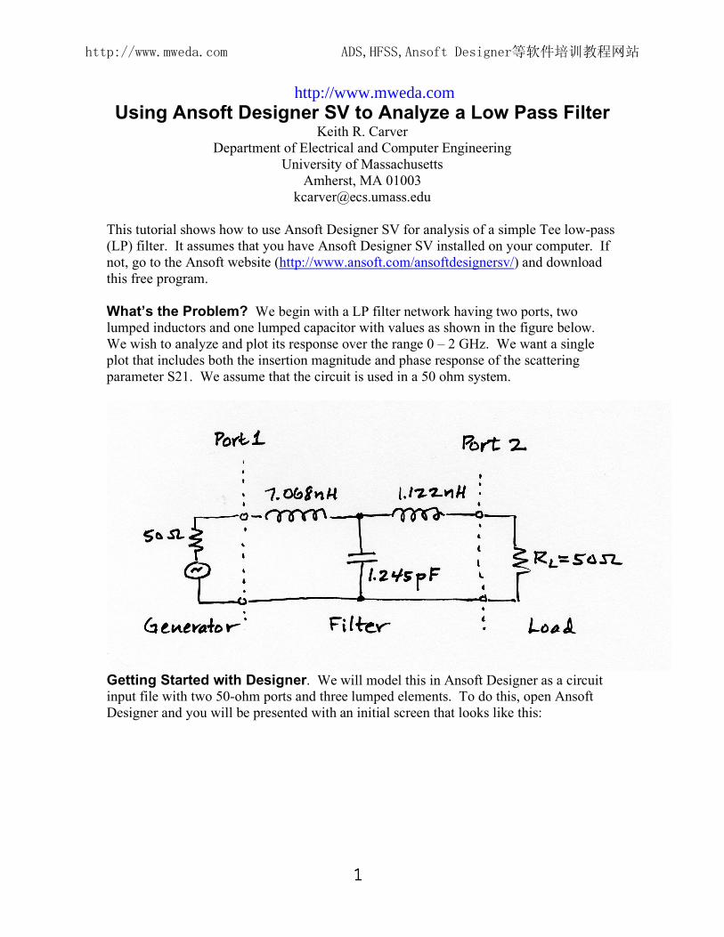
[email protected] This tutorial shows how to use Ansoft Designer SV for analysis of a simple Tee low-pass (LP) filter. It assumes that you have Ansoft Designer SV installed on your computer. If not, go to the Ansoft website (http://www.ansoft.com/ansoftdesignersv/) and download this free program. What’s the Problem? We begin with a LP filter network having two ports, two lumped inductors and one lumped capacitor with values as shown in the figure below. We wish to analyze and plot its response over the range 0 – 2 GHz. We want a single plot that includes both the insertion magnitude and phase response of the scattering parameter S21. We assume that the circuit is used in a 50 ohm system.
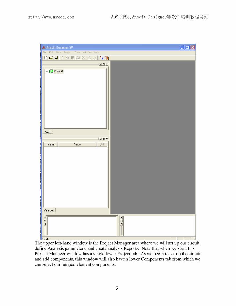
Getting Started with Designer. We will model this in Ansoft Designer as a circuit input file with two 50-ohm ports and three lumped elements. To do this, open Ansoft Designer and you will be presented with an initial screen that looks like this:
The upper left-hand window is the Project Manager area where we will set up our circuit, define Analysis parameters, and create analysis Reports. Note that when we start, this Project Manager window has a single lower Project tab. As we begin to set up the circuit and add components, this window will also have a lower Components tab from which we can select our lumped element components.
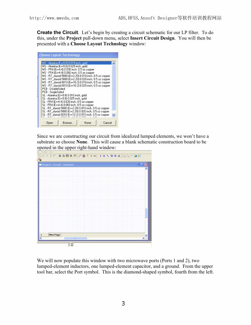
Create the Circuit. Let’s begin by creating a circuit schematic for our LP filter. To do this, under the Project pull-down menu, select Insert Circuit Design. You will then be presented with a Choose Layout Technology window:
Since we are constructing our circuit from idealized lumped elements, we won’t have a substrate so choose None. This will cause a blank schematic construction board to be opened in the upper right-hand window:
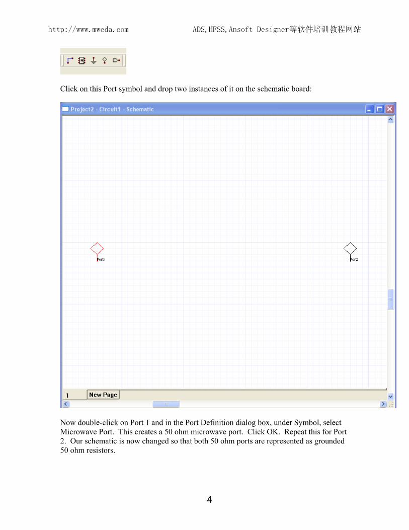
We will now populate this window with two microwave ports (Ports 1 and 2), two lumped-element inductors, one lumped-element capacitor, and a ground. From the upper tool bar, select the Port symbol. This is the diamond-shaped symbol, fourth from the left.
Click on this Port symbol and drop two instances of it on the schematic board:
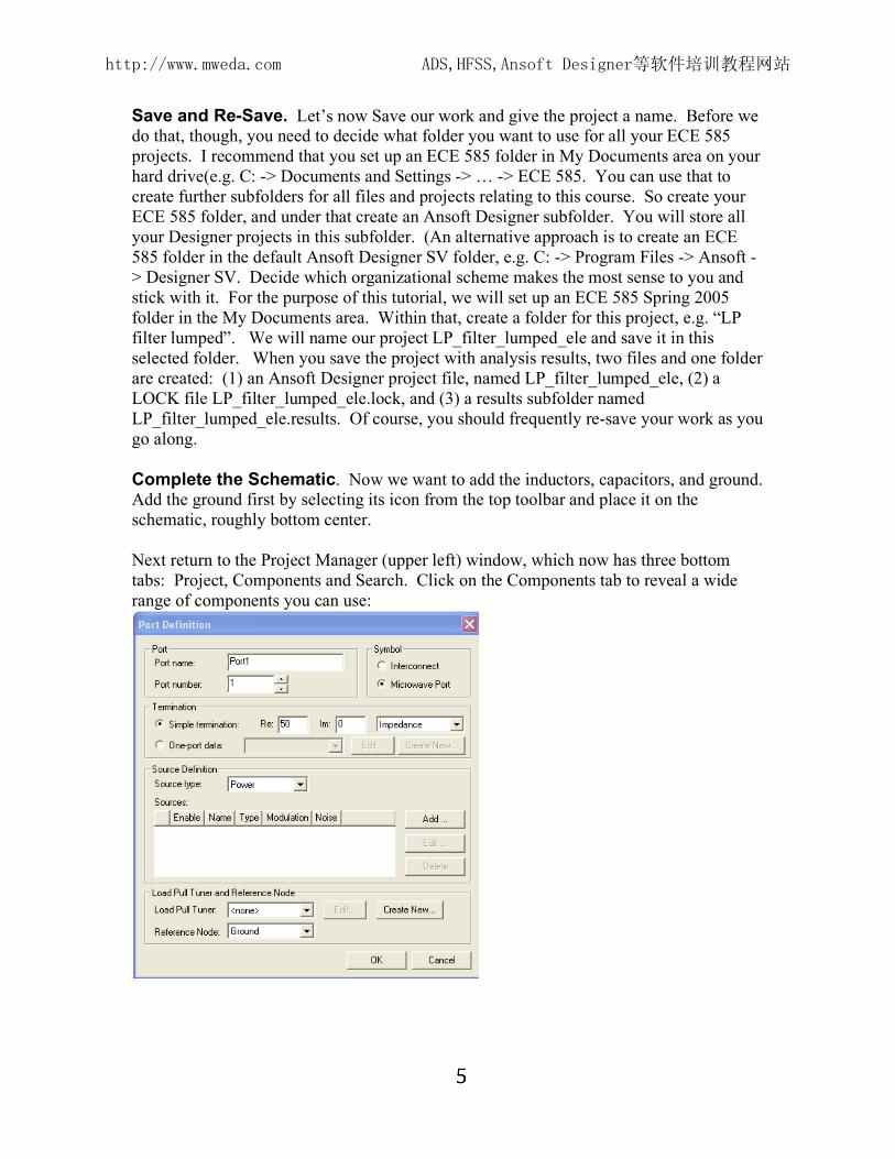
Now double-click on Port 1 and in the Port Definition dialog box, under Symbol, select Microwave Port. This creates a 50 ohm microwave port. Click OK. Repeat this for Port 2. Our schematic is now changed so that both 50 ohm ports are represented as grounded 50 ohm resistors.
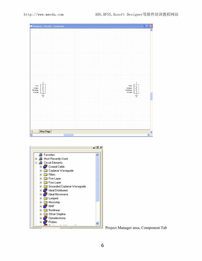
Save and Re-Save. Let’s now Save our work and give the project a name. Before we do that, though, you need to decide what folder you want to use for all your ECE 585 projects. I recommend that you set up an ECE 585 folder in My Documents area on your hard drive(e.g. C: -> Documents and Settings -> … -> ECE 585. You can use that to create further subfolders for all files and projects relating to this course. So create your ECE 585 folder, and under that create an Ansoft Designer subfolder. You will store all your Designer projects in this subfolder. (An alternative approach is to create an ECE 585 folder in the default Ansoft Designer SV folder, e.g. C: -> Program Files -> Ansoft -> Designer SV. Decide which organizational scheme makes the most sense to you and stick with it. For the purpose of this tutorial, we will set up an ECE 585 Spring 2005 folder in the My Documents area. Within that, create a folder for this project, e.g. “LP filter lumped”. We will name our project LP_filter_lumped_ele and save it in this selected folder. When you save the project with analysis results, two files and one folder are created: (1) an Ansoft Designer project file, named LP_filter_lumped_ele, (2) a LOCK file LP_filter_lumped_ele.lock, and (3) a results subfolder named LP_filter_lumped_ele.results. Of course, you should frequently re-save your work as you go along. Complete the Schematic. Now we want to add the inductors, capacitors, and ground. Add the ground first by selecting its icon from the top toolbar and place it on the schematic, roughly bottom center. Next return to the Project Manager (upper left) window, which now has three bottom tabs: Project, Components and Search. Click on the Components tab to reveal a wide range of components you can use:
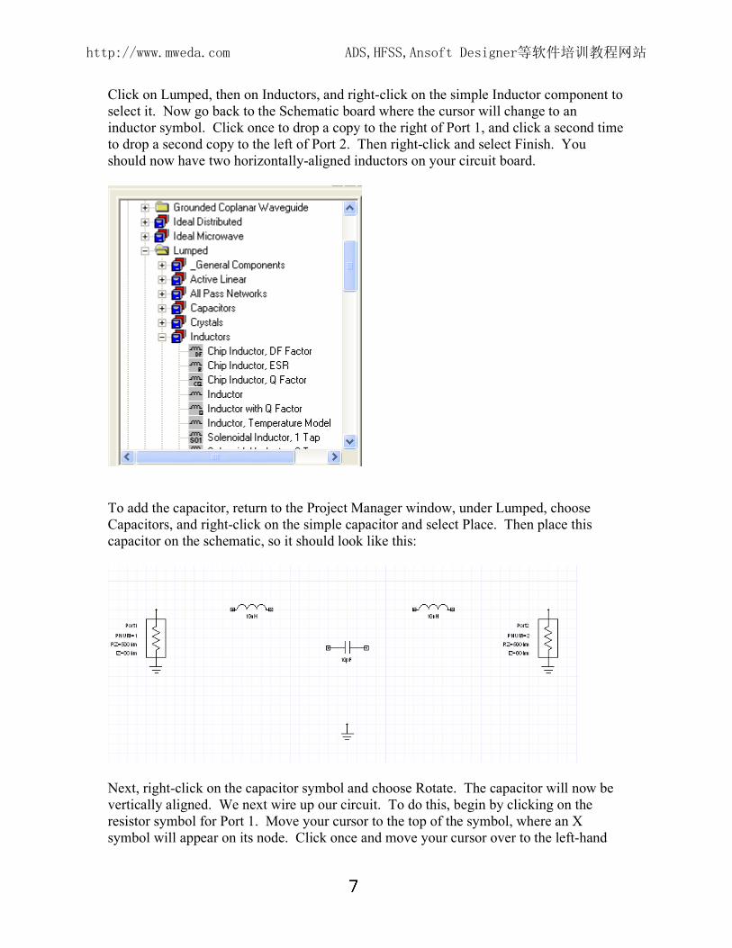
Click on Lumped, then on Inductors, and right-click on the simple Inductor component to select it. Now go back to the Schematic board where the cursor will change to an inductor symbol. Click once to drop a copy to the right of Port 1, and click a second time to drop a second copy to the left of Port 2. Then right-click and select Finish. You should now have two horizontally-aligned inductors on your circuit board.
To add the capacitor, return to the Project Manager window, under Lumped, choose Capacitors, and right-click on the simple capacitor and select Place. Then place this capacitor on the schematic, so it should look like this:
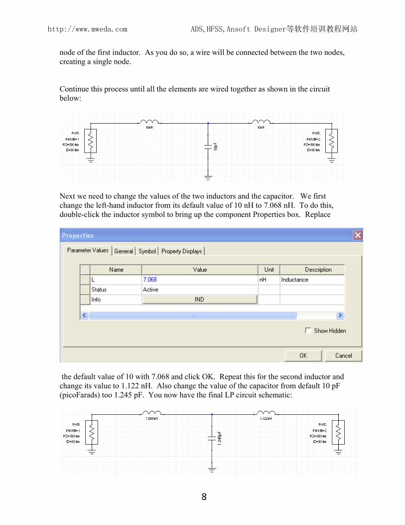
Next, right-click on the capacitor symbol and choose Rotate. The capacitor will now be vertically aligned. We next wire up our circuit. To do this, begin by clicking on the resistor symbol for Port 1. Move your cursor to the top of the symbol, where an X symbol will appear on its node. Click once and move your cursor over to the left-hand
node of the first inductor. As you do so, a wire will be connected between the two nodes, creating a single node. Continue this process until all the elements are wired together as shown in the circuit below:
Next we need to change the values of the two inductors and the capacitor. We first change the left-hand inductor from its default value of 10 nH to 7.068 nH. To do this, double-click the inductor symbol to bring up the component Properties box. Replace
the default value of 10 with 7.068 and click OK. Repeat this for the second inductor and change its value to 1.122 nH. Also change the value of the capacitor from default 10 pF (picoFarads) too 1.245 pF. You now have the final LP circuit schematic:
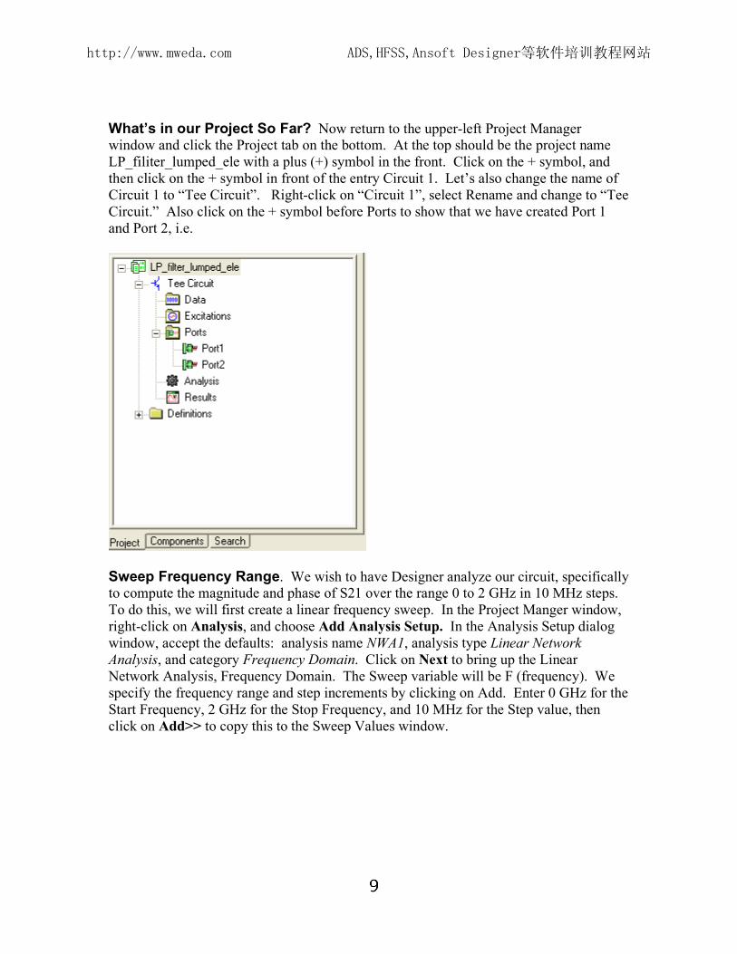
What’s in our Project So Far? Now return to the upper-left Project Manager window and click the Project tab on the bottom. At the top should be the project name LP_filiter_lumped_ele with a plus (+) symbol in the front. Click on the + symbol, and then click on the + symbol in front of the entry Circuit 1. Let’s also change the name of Circuit 1 to “Tee Circuit”. Right-click on “Circuit 1”, select Rename and change to “Tee Circuit.” Also click on the + symbol before Ports to show that we have created Port 1 and Port 2, i.e.
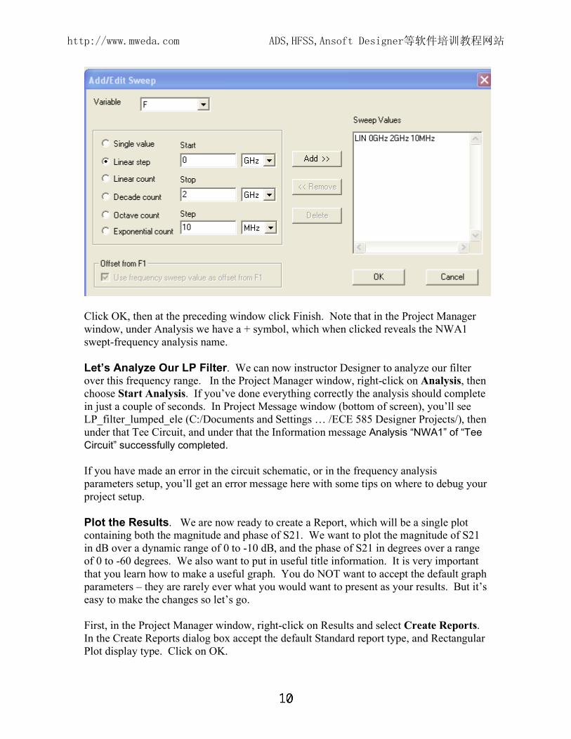
Sweep Frequency Range. We wish to have Designer analyze our circuit, specifically to compute the magnitude and phase of S21 over the range 0 to 2 GHz in 10 MHz steps. To do this, we will first create a linear frequency sweep. In the Project Manger window, right-click on Analysis, and choose Add Analysis Setup. In the Analysis Setup dialog window, accept the defaults: analysis name NWA1, analysis type Linear Network Analysis, and category Frequency Domain. Click on Next to bring up the Linear Network Analysis, Frequency Domain. The Sweep variable will be F (frequency). We specify the frequency range and step increments by clicking on Add. Enter 0 GHz for the Start Frequency, 2 GHz for the Stop Frequency, and 10 MHz for the Step value, then click on Add>> to copy this to the Sweep Values window.
Click OK, then at the preceding window click Finish. Note that in the Project Manager window, under Analysis we have a + symbol, which when clicked reveals the NWA1 swept-frequency analysis name. Let’s Analyze Our LP Filter. We can now instructor Designer to analyze our filter over this frequency range. In the Project Manager window, right-click on Analysis, then choose Start Analysis. If you’ve done everything correctly the analysis should complete in just a couple of seconds. In Project Message window (bottom of screen), you’ll see LP_filter_lumped_ele (C:/Documents and Settings … /ECE 585 Designer Projects/), then under that Tee Circuit, and under that the Information message Analysis “NWA1” of “Tee Circuit” successfully completed. If you have made an error in the circuit schematic, or in the frequency analysis parameters setup, you’ll get an error message here with some tips on where to debug your project setup. Plot the Results. We are now ready to create a Report, which will be a single plot containing both the magnitude and phase of S21. We want to plot the magnitude of S21 in dB over a dynamic range of 0 to -10 dB, and the phase of S21 in degrees over a range of 0 to -60 degrees. We also want to put in useful title information. It is very important that you learn how to make a useful graph. You do NOT want to accept the default graph parameters – they are rarely ever what you would want to present as your results. But it’s easy to make the changes so let’s go. First, in the Project Manager window, right-click on Results and select Create Reports. In the Create Reports dialog box accept the default Standard report type, and Rectangular Plot display type. Click on OK.
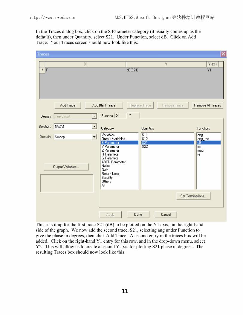
In the Traces dialog box, click on the S Parameter category (it usually comes up as the default), then under Quantity, select S21. Under Function, select dB. Click on Add Trace. Your Traces screen should now look like this:
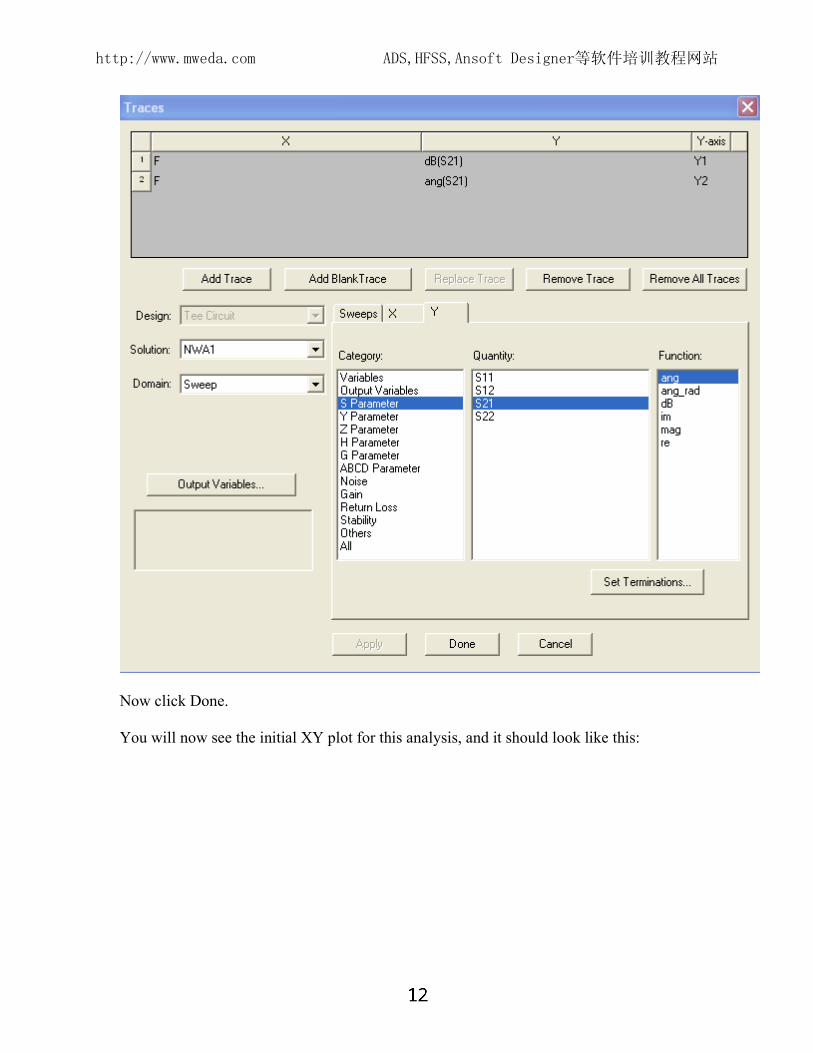
This sets it up for the first trace S21 (dB) to be plotted on the Y1 axis, on the right-hand side of the graph. We now add the second trace, S21, selecting ang under Function to give the phase in degrees, then click Add Trace. A second entry in the traces box will be added. Click on the right-hand Y1 entry for this row, and in the drop-down menu, select Y2. This will allow us to create a second Y axis for plotting S21 phase in degrees. The resulting Traces box should now look like this:
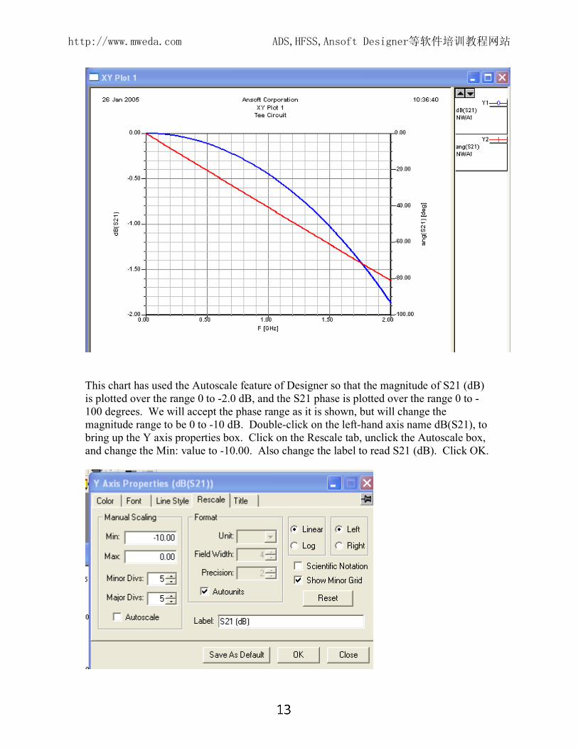
This chart has used the Autoscale feature of Designer so that the magnitude of S21 (dB) is plotted over the range 0 to -2.0 dB, and the S21 phase is plotted over the range 0 to -100 degrees. We will accept the phase range as it is shown, but will change the magnitude range to be 0 to -10 dB. Double-click on the left-hand axis name dB(S21), to bring up the Y axis properties box. Click on the Rescale tab, unclick the Autoscale box, and change the Min: value to -10.00. Also change the label to read S21 (dB). Click OK.
We now need to add more information to the title. The default title bar will have today’s date on the left-hand side, and the time on the right-hand side. The “Ansoft Corporation” top center is inserted by default and cannot be changed. The default graph title will be XY Plot, which doesn’t tell the reader anything. We want to provide more detailed information about this project, including your name. On the graph, double-click on the top title to bring up the Title Properties dialog box. Click on Title, and add your name just after today’s date. Change the graph title to S21 magnitude and phase response, and change the User Subtitle to LP filter with lumped elements.
Next, choose the Font tab, and under Font Style deselect the boldface by choosing Regular. This will change all axis labels and graph title to Regular, but will leave the User Subtitle in Boldface. The User Subtitle should be a short description of your circuit, but the graph title should be a word description of this particular graph. Let’s make one more addition. Right-click anywhere on the graph, and select Add Label. In the Label dialog box, enter S21 (dB) and place this label near the magnitude (blue) trace. Repeat this and enter a S21 (deg) label near the phase (red) trace. When there are two traces on the same graph, this is a big help to the reader, who is likely to be me! Even though the legend has this information at the top right, it is less intuitive than putting the label directly on the graph. Your graph should now look like this:
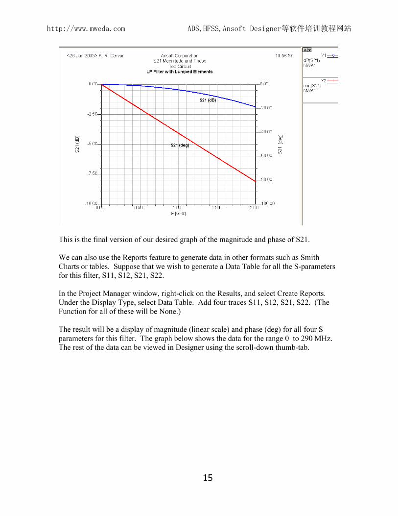
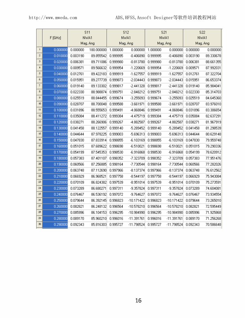
This is the final version of our desired graph of the magnitude and phase of S21. We can also use the Reports feature to generate data in other formats such as Smith Charts or tables. Suppose that we wish to generate a Data Table for all the S-parameters for this filter, S11, S12, S21, S22. In the Project Manager window, right-click on the Results, and select Create Reports. Under the Display Type, select Data Table. Add four traces S11, S12, S21, S22. (The Function for all of these will be None.) The result will be a display of magnitude (linear scale) and phase (deg) for all four S parameters for this filter. The graph below shows the data for the range 0 to 290 MHz. The rest of the data can be viewed in Designer using the scroll-down thumb-tab.