Using the TPS54335A to Create an Inverting Power Supply
Application ReportSLVA910A–July 2017–Revised July 2017
Using the TPS54335A to Create an Inverting Power Supply
MiloZhu
ABSTRACTSome applications, like audio amplifiers, line drivers, and receivers, require a positive input voltage togenerate a negative output voltage. This application report presents a solution for creating an invertingpower supply using a synchronous buck converter, TPS54335A. The purpose of this application report isto discuss the steps to create a negative power supply using the TPS54335A.
Using the TPS54335A to Create an Inverting Power Supply
1 Application DescriptionFor a 28-V, 2-A or 3-A solution that covers 12-V, 19-V, and 24 -V power rail applications, TI has a miserfamily that includes the TPS54231, TPS54331, and TPS54232 devices, but these parts arenonsynchronous. A reference design is available online for inverting power supply applications (seePMP4748, TPS54232).
Using these nonsynchronous converters for inverting power supply has certain disadvantages, like lowerefficiency because of the rectifier diode, and a slight voltage bump during soft-start because of theswitching frequency fold-back.
Integrating a tight BOM size is becoming more popular. For a 28-V, 3-A solution, the synchronous partTPS54335A supports 4.5-V to 28-V input and output up to 3 A with adjustable switching frequency. Anincreasing number of customers prefer to choose synchronous solution for their inverting supplyapplication.
This application report discusses how to design an inverting regulator step-by-step using the TPS54335A,as well as component selection criteria and equations, and some captured waveforms.
2 Design Consideration and Procedures
2.1 Choosing the Correct Buck Converter for Inverting Power ApplicationsWhen choosing a buck converter for inverting power applications, users must consider certainspecifications to determine whether the converter meets the application requirement or not. Thesespecifications include:• Output voltage range• Input voltage range• Allowable duty cycle• Maximum output current
2.1.1 Output Voltage RangeThe difference between the maximum input voltage and output voltage must not exceed the maximumoperating voltage of the device. For the TPS54335A, the maximum operating voltage is 28 V. Forexample, if the output is –5 V, then the maximum input voltage, VIN(max), could be as high as 23 V, whichcan support a 19-V power rail application.
2.1.2 Input Voltage RangeThe minimum operating input voltage of the inverting power supply, VIN(min), must be greater than theminimum device operating voltage. For the TPS54335A, the minimum input voltage is 4.5 V, so theinverting power supply input voltage must be higher than 4.5 V.
2.1.3 Duty CycleEquation 1 shows the ideal duty cycle for the inverting power supply, neglecting the losses of the power-switching inductor. The output voltage, VOUT, is negative and the input voltage, VIN, is positive.
(1)
The maximum duty cycle, Dmax, is calculated using the minimum input voltage as a substitution for theinput voltage. Similarly, Dmin is evaluated using the maximum input voltage, VIN(max).
Using the TPS54335A to Create an Inverting Power Supply
2.1.4 Output CurrentUse Equation 2 to estimate whether the selected switching regulator can deliver the output current. Theuser must know the minimum current limit of the device, ICL(min), maximum duty cycle, Dmax, and theinductor ripple current value, ILripple.
(2)
For the TPS54335A, the minimum high-side current is 4 A, assume the ILripple is 25% of the minimumcurrent limit, and Dmax is 0.294 (–5 V / (12 V– (–5 V))), then get the max capable of delivering outputcurrent is 2.8 A.
2.1.5 Operating FrequencySelecting an operating frequency is a trade-off between size and thermal performance. Higher frequenciesrequire lower-valued inductors with smaller sizes, which introduces higher switching loss with lowerefficiency and higher temperature.
For the TPS54335A, switching frequency is adjustable from 50 kHz to 1.5 MHz using one externalresistor. Use Equation 3 to calculate the resistor.
(3)
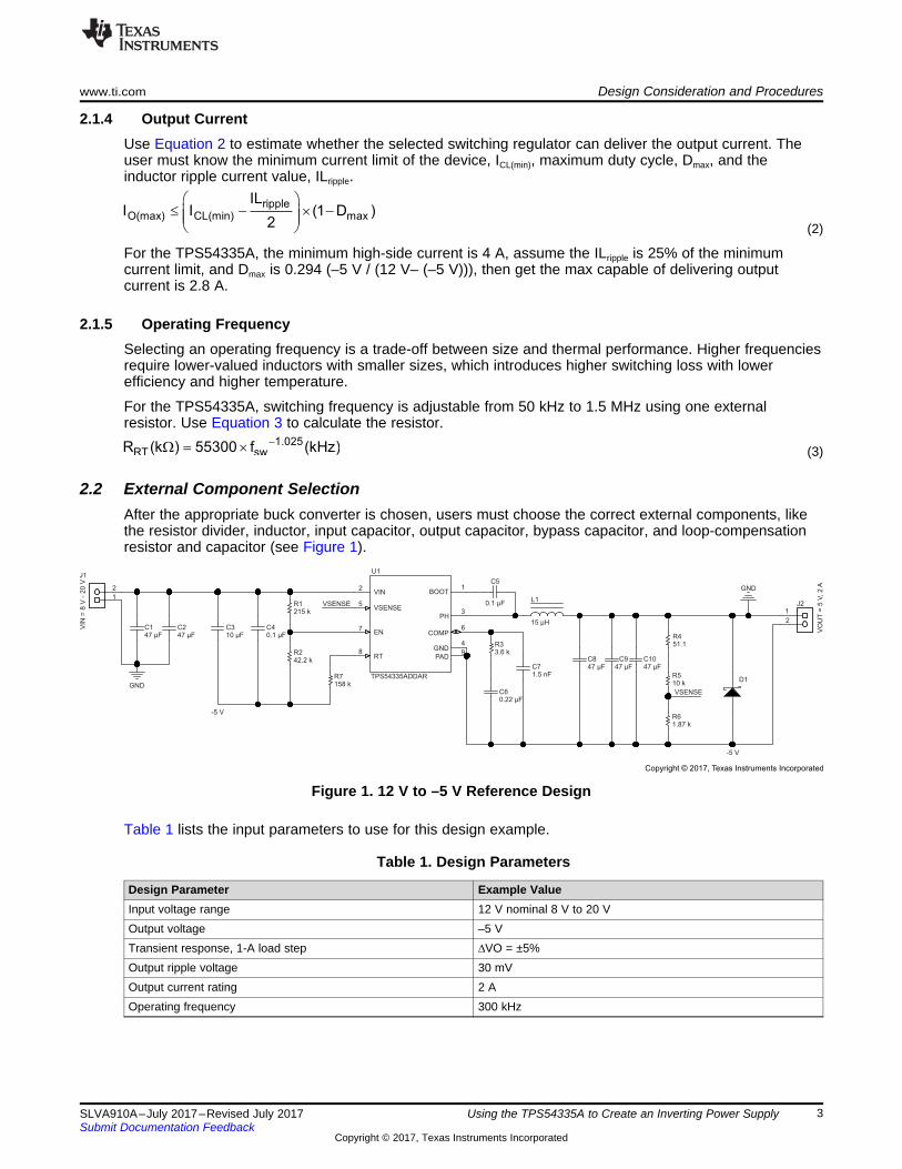
2.2 External Component SelectionAfter the appropriate buck converter is chosen, users must choose the correct external components, likethe resistor divider, inductor, input capacitor, output capacitor, bypass capacitor, and loop-compensationresistor and capacitor (see Figure 1).
Figure 1. 12 V to –5 V Reference Design
Table 1 lists the input parameters to use for this design example.
Table 1. Design Parameters
Design Parameter Example ValueInput voltage range 12 V nominal 8 V to 20 VOutput voltage –5 VTransient response, 1-A load step ∆VO = ±5%Output ripple voltage 30 mVOutput current rating 2 AOperating frequency 300 kHz
Using the TPS54335A to Create an Inverting Power Supply
2.2.1 Frequency Set ResistorThe switching frequency of the TPS54335A is set at 300 kHz. Use Equation 3 to calculate the requiredvalue for RRT. The calculated value is 159.8 kΩ. Use the next smaller, standard value of 158 kΩ for RRT.
2.2.2 Resistor DividerThe output voltage of the TPS54335A device is externally adjustable using a resistor divider network. Inthis example, this divider network is comprised of R5 and R6. Use Equation 4 and Equation 5 to calculatethe relationship of the output voltage to the resistor divider.
(4)
(5)
For this design:• Vref = 0.8 V• Set R5 = 10 kΩ and R6 = 1.87 kΩ• The 51.1-Ω resistor R4 is provided as a convenient location to break the control loop for stability
testing.
2.2.3 InductorTo determine the inductor value, use Equation 6 to calculate the average inductor current, ILavg, at themaximum output current and maximum duty. Assuming that the maximum output current, IOUT, is 2 A andusing the maximum duty cycle, Dmax is 0.385 (5 V / (8 V – (–5 V)) = 0.385), here ILavg is 3.25 A.
(6)
Assuming VIN(max) of 20 V, ILavg of 3.25 A, and ƒsw of 300 kHz, use Equation 7 to calculate LO, whichis 16.5 µH. The nearest standard inductor of 15 µH is used.
(7)
The inductor saturation current must be greater than the 3.59 A of peak current calculated in Equation 8.
(8)
The inductor rms current must be greater than the 2.84 A of peak current calculated in Equation 9.
(9)
2.2.4 Output CapacitorThe output capacitor must supply the current when the high-side switch is off. Use the minimum inputvoltage to calculate the output capacitance needed. This need occurs when the duty cycle and the peak-to-peak current in the output capacitor are the maximum. Using the 0.5% voltage ripple specification, VOUT,and Equation 10, CO(min) is calculated to be 103 µF.
Using the TPS54335A to Create an Inverting Power Supply
Assuming the 0.5% voltage ripple and maximum duty cycle, the RC equivalent series resistance must beless than 69.6 mΩ (see Equation 11).
(11)
Use Equation 12 to calculate the rms current for the output capacitor, which is 1.58 A . Three 47-µF, 10-VX7R in parallel are used for the output capacitor because of the low ESR and size.
(12)
2.2.5 Input CapacitorsThe input capacitors between VIN and ground are used to limit the voltage ripple of the input supply.
Equation 13, Equation 14, Equation 15, and Equation 16 are used to estimate the capacitance, maximumESR, and current rating for the input capacitor, Ci.
(13)
Equation 14 is used to estimate the average input current, which is 1.25 A.
(14)
Equation 14 and Equation 15 are used to calculate the minimum required input capacitance, which is 52µF and the maximum ESR, which is 64 mΩ.
(15)
Using Equation 16, the input capacitor needs a current rating of at least 1.78 A . Two 47-µF, 35-V X7R inparallel are used for the input capacitor because of the low ESR and size.
(16)
2.2.6 Bypass CapacitorThe TPS54335A device needs a tightly coupled, ceramic bypass capacitor, connected to the VIN and GNDpin of the device. Because the device GND is the power supply output voltage, the voltage rating of thecapacitor must be greater than the differences in the maximum input and output voltage of the powersupply.
A minimum of 10 µF from the VIN pin to GND is recommended for the TPS54335A device. Another 0.1-µFcapacitor has been added as a bypass capacitor to clear high-frequency noise.
2.2.7 Frequency Response of the Inverting RegulatorUsing a buck boost regulator to generate a negative output voltage does not close the feedback loop likeusing a buck power supply, so a different design method is needed. The inverting power supply transferfunction has two zeroes and a pole.
Using the TPS54335A to Create an Inverting Power Supply
Equation 17 is a simplified transfer function of an inverting power supply.
(17)
In Equation 18, the ESR zero, ƒz1, is the same as in a buck regulator, and is a function of the outputcapacitor and its ESR.
(18)
The other zero is a right half plane zero, ƒz2. The frequency response of ƒz2 results in an increasing gainand a decreasing phase. The ƒz2 frequency is a function of the duty cycle, output current, and theinductor. Equation 19 shows the calculated minimum frequency of ƒz2, which is used to determine thecrossover frequency.
(19)
The dominant pole, ƒp1, is a function of the load current, output capacitor, and duty cycle (seeEquation 20).
(20)
In Equation 21, Kbb is the DC gain and is used to calculate the frequency compensation components. Thegmps variable is the transconductance of the power stage, which is 8 A / V for the TPS54335A device.
(21)
Here, ƒz1 is estimated to be 225.9 kHz. The output capacitor ESR is assumed to be 5 m. Here, ƒz2 isestimated to be 26.3 kHz. Assuming resistance of the inductor, Rdc is 20 m. Here, ƒp1 is estimated to be425 Hz assuming a nominal duty cycle. Kbb is calculated as 10.9 V/V using Equation 21, assumingnominal input voltage and gmps as 8 A/V.
The crossover of the power supply should be set between the ƒp1 frequency and 1/3 of the ƒz2frequency. TI recommends starting with the crossover frequency, ƒco, given by Equation 22. Here, ƒco isestimated to be 3.34 kHz.
(22)
Use Equation 23 to calculate the compensation resistor, Rcomp, needed to set the compensation gain at thefco frequency. For the TPS54335A device, Vref is 0.8 V and gmea is 1300 µA/V. In Equation 23 Rcomp isequal to 3.46 kΩ. Use the nearest standard value of 3.5 kΩ.
(23)
The compensation zero, Czero, is set to 1/2 of the dominant pole, ƒp1. To calculate the czero, useEquation 24, which results in 0.22 µF. Use the next larger standard value of 0.22 µF.
Using the TPS54335A to Create an Inverting Power Supply
The compensation pole, Cpole, is set to equal the RHP zero, ƒz2. Use Equation 25 to calculate cpole, whichresults in 1.75 nF. Use the next standard value of 1.5 nF.
(25)
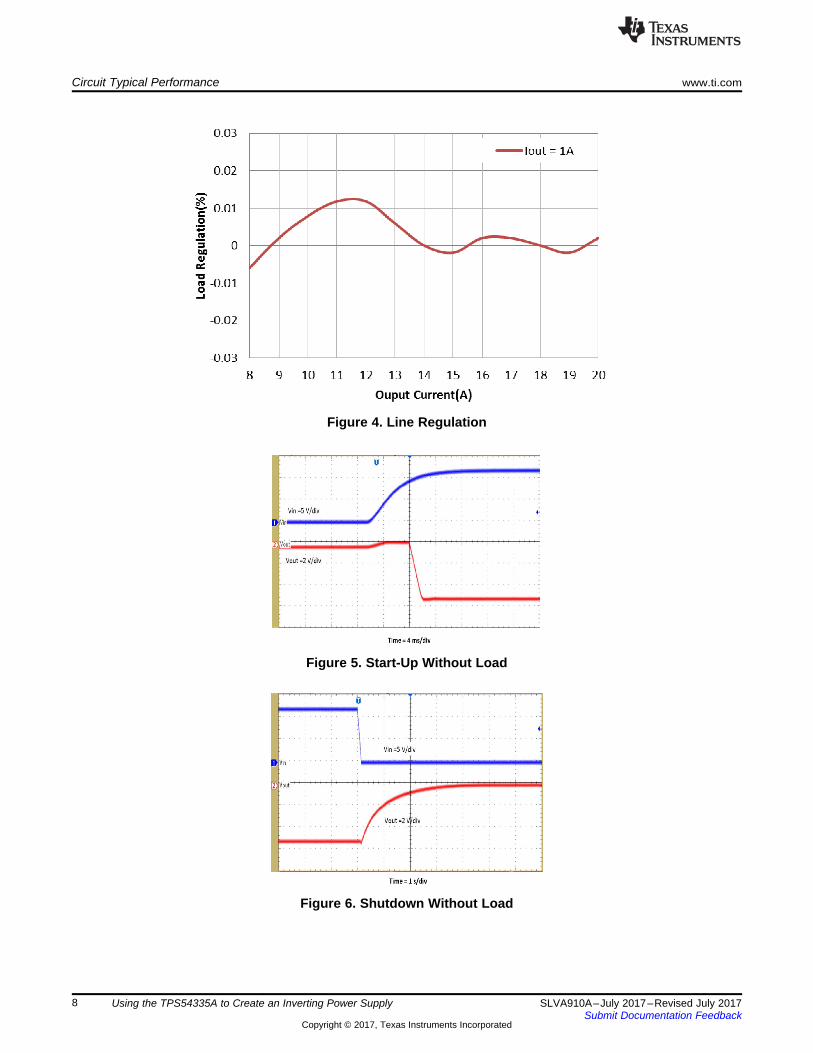
3 Circuit Typical PerformanceThe design shown in Figure 1 was used to generate –5-V output from 12-V input. Figure 2 to Figure 13show some typical measured waveforms of this design.
Using the TPS54335A to Create an Inverting Power Supply
Figure 13. Bode Plot
4 ConclusionThe TPS54335A buck converter can be configured as an inverting buck boost converter to generate anegative output voltage. This application report explains how to select the external components. Measureddata from the example design are provided. This application report also applies to the TPS54336A andTPS54334 devices.
5 References• Texas Instruments, TPS5433xA 4.5-V to 28-V Input, 3-A Output, Synchronous Step-Down DC-DC
Converter, data sheet• Texas Instruments, Using a Buck Converter in an Inverting Buck-Boost Topology, technical brief• Texas Instruments, Create an Inverting Power Supply Using a Synchronous Step-Down Regulator,
application report• Texas Instruments, Create an Inverting Power Supply From a Step-Down Regulator, application report
Revision HistoryNOTE: Page numbers for previous revisions may differ from page numbers in the current version.
Changes from July 13, 2017 to July 19, 2017 .................................................................................................................. Page
• Changed R2, L1, and R4 values in 12 V to –5 V Reference Design figure ....................................................... 3
IMPORTANT NOTICE FOR TI DESIGN INFORMATION AND RESOURCES
Texas Instruments Incorporated (‘TI”) technical, application or other design advice, services or information, including, but not limited to,reference designs and materials relating to evaluation modules, (collectively, “TI Resources”) are intended to assist designers who aredeveloping applications that incorporate TI products; by downloading, accessing or using any particular TI Resource in any way, you(individually or, if you are acting on behalf of a company, your company) agree to use it solely for this purpose and subject to the terms ofthis Notice.TI’s provision of TI Resources does not expand or otherwise alter TI’s applicable published warranties or warranty disclaimers for TIproducts, and no additional obligations or liabilities arise from TI providing such TI Resources. TI reserves the right to make corrections,enhancements, improvements and other changes to its TI Resources.You understand and agree that you remain responsible for using your independent analysis, evaluation and judgment in designing yourapplications and that you have full and exclusive responsibility to assure the safety of your applications and compliance of your applications(and of all TI products used in or for your applications) with all applicable regulations, laws and other applicable requirements. Yourepresent that, with respect to your applications, you have all the necessary expertise to create and implement safeguards that (1)anticipate dangerous consequences of failures, (2) monitor failures and their consequences, and (3) lessen the likelihood of failures thatmight cause harm and take appropriate actions. You agree that prior to using or distributing any applications that include TI products, youwill thoroughly test such applications and the functionality of such TI products as used in such applications. TI has not conducted anytesting other than that specifically described in the published documentation for a particular TI Resource.You are authorized to use, copy and modify any individual TI Resource only in connection with the development of applications that includethe TI product(s) identified in such TI Resource. NO OTHER LICENSE, EXPRESS OR IMPLIED, BY ESTOPPEL OR OTHERWISE TOANY OTHER TI INTELLECTUAL PROPERTY RIGHT, AND NO LICENSE TO ANY TECHNOLOGY OR INTELLECTUAL PROPERTYRIGHT OF TI OR ANY THIRD PARTY IS GRANTED HEREIN, including but not limited to any patent right, copyright, mask work right, orother intellectual property right relating to any combination, machine, or process in which TI products or services are used. Informationregarding or referencing third-party products or services does not constitute a license to use such products or services, or a warranty orendorsement thereof. Use of TI Resources may require a license from a third party under the patents or other intellectual property of thethird party, or a license from TI under the patents or other intellectual property of TI.TI RESOURCES ARE PROVIDED “AS IS” AND WITH ALL FAULTS. TI DISCLAIMS ALL OTHER WARRANTIES ORREPRESENTATIONS, EXPRESS OR IMPLIED, REGARDING TI RESOURCES OR USE THEREOF, INCLUDING BUT NOT LIMITED TOACCURACY OR COMPLETENESS, TITLE, ANY EPIDEMIC FAILURE WARRANTY AND ANY IMPLIED WARRANTIES OFMERCHANTABILITY, FITNESS FOR A PARTICULAR PURPOSE, AND NON-INFRINGEMENT OF ANY THIRD PARTY INTELLECTUALPROPERTY RIGHTS.TI SHALL NOT BE LIABLE FOR AND SHALL NOT DEFEND OR INDEMNIFY YOU AGAINST ANY CLAIM, INCLUDING BUT NOTLIMITED TO ANY INFRINGEMENT CLAIM THAT RELATES TO OR IS BASED ON ANY COMBINATION OF PRODUCTS EVEN IFDESCRIBED IN TI RESOURCES OR OTHERWISE. IN NO EVENT SHALL TI BE LIABLE FOR ANY ACTUAL, DIRECT, SPECIAL,COLLATERAL, INDIRECT, PUNITIVE, INCIDENTAL, CONSEQUENTIAL OR EXEMPLARY DAMAGES IN CONNECTION WITH ORARISING OUT OF TI RESOURCES OR USE THEREOF, AND REGARDLESS OF WHETHER TI HAS BEEN ADVISED OF THEPOSSIBILITY OF SUCH DAMAGES.You agree to fully indemnify TI and its representatives against any damages, costs, losses, and/or liabilities arising out of your non-compliance with the terms and provisions of this Notice.This Notice applies to TI Resources. Additional terms apply to the use and purchase of certain types of materials, TI products and services.These include; without limitation, TI’s standard terms for semiconductor products http://www.ti.com/sc/docs/stdterms.htm), evaluationmodules, and samples (http://www.ti.com/sc/docs/sampterms.htm).