Page 1
Polarized spin and valley transport across ferromagnetic silicene junctionsV. Vargiamidis, and P. Vasilopoulos
Citation: Journal of Applied Physics 117, 094305 (2015);View online: https://doi.org/10.1063/1.4913934View Table of Contents: http://aip.scitation.org/toc/jap/117/9Published by the American Institute of Physics
Articles you may be interested inValley and spin thermoelectric transport in ferromagnetic silicene junctionsApplied Physics Letters 104, 202401 (2014); 10.1063/1.4876927
Perfect spin-valley filter controlled by electric field in ferromagnetic siliceneJournal of Applied Physics 115, 023706 (2014); 10.1063/1.4861644
Electric- and exchange-field controlled transport through silicene barriers: Conductance gap and near-perfectspin polarizationApplied Physics Letters 105, 223105 (2014); 10.1063/1.4903248
Valley and spin resonant tunneling current in ferromagnetic/nonmagnetic/ferromagnetic silicene junctionAIP Advances 6, 025307 (2016); 10.1063/1.4942043
Gate-tunable valley-spin filtering in silicene with magnetic barrierJournal of Applied Physics 117, 203903 (2015); 10.1063/1.4921799
Resonant spin and valley polarization in ferromagnetic silicene quantum wellApplied Physics Letters 104, 032105 (2014); 10.1063/1.4863091
Page 2
Polarized spin and valley transport across ferromagnetic silicene junctions
V. Vargiamidis and P. VasilopoulosDepartment of Physics, Concordia University, 7141 Sherbrooke Ouest Montr�eal, Qu�ebec H4B 1R6, Canada
(Received 23 December 2014; accepted 20 February 2015; published online 5 March 2015)
We study ballistic transport of Dirac fermions through silicene barriers, of width d, with an
exchange field M and metallic gates above them that provide tunable potentials of height U. Away
from the Dirac point (DP), the spin- and valley-resolved conductances, as functions of U, exhibit
resonances and close to it a pronounced dip that becomes a transport gap when an appropriate elec-
tric field Ez is applied. The charge conductance gc of such a junction changes from oscillatory to a
monotonically decreasing function of d beyond a critical Ez. This change of gc can be used to real-
ize electric-field-controlled switching. The field M splits each resonance of gc in two spin-resolved
peaks. The spin ps and valley pv polarizations of the current near the DP increase with Ez or M and
become nearly perfect above certain of their values. We also show that ps and pv can be inverted
either by reversing the polarity of U or the direction of M. For two barriers, there is no splitting in
gc when the fields M are in opposite directions. Most of these phenomena have no analogs in gra-
phene. VC 2015 AIP Publishing LLC. [http://dx.doi.org/10.1063/1.4913934]
I. INTRODUCTION
Silicene, a monolayer of silicon atoms forming a two-
dimensional (2D) honeycomb lattice, has been predicted to
be stable1 and several attempts have been made to synthesize
it.2,3 This new material has attracted considerable attention4
due to the fact that it has Dirac cones which are similar to
those of graphene.5 However, contrary to graphene, silicene
has a strong intrinsic spin-orbit interaction (SOI) which to-
gether with its buckled geometry leads to a gap approxi-
mately 1.55 meV wide6,7 in the low-energy Dirac-like band
structure. The buckled structure is a remarkable property of
silicene that graphene does not possess and can facilitate the
control7,8 of its band gap by the application of an external
perpendicular electric field Ez. Accordingly, silicene can
overcome difficulties associated with potential applications
of graphene in nanoelectronics (lack of a controllable gap)
due to the available spin and valley degrees of freedom. This
and its compatibility with silicon-based technology led to
studies of important effects, such as the spin- and valley-Hall
effects,6,9–12 the quantum anomalous Hall effect,8,13 and
spin-valley coupling,14 to name but a few. For a recent
review see Ref. 15.
Spintronics aim to inject, manipulate, and/or use the spin
degree of freedom in electronic devices. In contrast with gra-
phene, the large value of SOI in silicene16 not only can lead to
spin-resolved transport but also to a cross correlation between
the valley and spin degrees of freedom. Furthermore, silicon
has a longer spin-diffusion time17,18 and spin-coherence
length19 compared with graphene,20 thus making silicene
appear more suitable for spintronics applications.
In earlier works, several novel features have been studied,
such as ferromagnetic (FM) correlations21 and resonant trans-
port through double barriers22 in graphene, the anomalous mag-
netoresistance,23 a valley-polarized quantum anomalous Hall
effect in the presence of exchange,24 and the conductance25
across FM strips on the surface of a topological insulator, and
valley and spin transport in FM silicene.26,27 However, several
important effects of the electric and exchange fields on trans-
port of Dirac fermions in FM silicene have not been studied so
far. Contrary to graphene, the field Ez greatly influences the
transport properties of FM silicene because its band structures
near the K and K0 points shift in different ways.13 This makes
possible the control of spin and valley transport.
In this work, we systematically study charge, spin, and
valley transport in silicene with a FM insulator on top of the
sample and a metallic gate above it. The normal metal gate
allows one to control the Fermi level locally and create a tun-
able barrier in silicene. First, we show that the charge con-
ductance gc through the junction can be either an oscillatory
or a monotonically decaying function of the junction width
d. One can interpolate between these two qualitatively differ-
ent behaviours of gc by varying Ez. Second, we show that gc
develops a transport gap with increasing Ez in an interval
symmetric with respect to the Dirac point (DP). The physical
origin of this gap is the fact that Ez acts like an extra
“barrier”: it does so for Ez large enough that transport via
evanescent modes is completely suppressed. Notice that our
subject differs from that of Ref. 28 in which different
exchange fields apply to the two sublattices but no barrier is
present and transport is not considered. Here we study trans-
port properties in the presence of barriers and exchange
fields which are the same for both sublattices and exist only
in the barrier regions. In this way we can control the charge,
spin, and valley conductances and the spin/valley polariza-
tions by varying the barrier parameters and/or the exchange
fields. Our study also differs from that of Ref. 24 which
involves a uniform exchange field and no barriers.
Furthermore, we demonstrate that the presence of the
FM insulator induces exchange splittings in silicene which
are similar to those in graphene.21 Due to the exchange split-
tings, the spin polarization near the DP increases with Ez or
M and becomes nearly perfect above certain of their values.
In addition, the spin and valley polarizations can be inverted
either by changing the gate voltage U from negative to
0021-8979/2015/117(9)/094305/11/$30.00 VC 2015 AIP Publishing LLC117, 094305-1
JOURNAL OF APPLIED PHYSICS 117, 094305 (2015)
Page 3
positive or by reversing the direction of M. We also study
the case of two magnetic gates a distance b apart. We find
that the spin-up and spin-down conductances become identi-
cal when the exchange fields are in opposite directions and
of equal magnitude resulting in the absence of exchange
splittings. The results constitute a significant extension of
our recent work.29 In particular, the valley polarization in
itself, the spin and valley polarization reversals just stated,
an interpretation of the conductance behaviour vs the field
Ez, with the help of the band structure near the two valleys,
and some other results on single and double barriers are not
part of this work.
The rest of the paper is organized as follows. In Sec. II, we
present the calculation of the spin- and valley-resolved conduct-
ance through a FM junction in silicene and show that the charge
conductance can be controlled with Ez. In Sec. III, we discuss
the effects of the exchange field on the charge, spin, and valley
transport, while in Sec. IV, we present our results for a double
FM junction. Finally, we conclude with a summary in Sec. V.
II. TRANSPORT THROUGH A FERROMAGNETICJUNCTION
We study ballistic electron transport across a FM strip in
silicene with a metallic gate above it which extends over a
region of width d (see Fig. 1(a)). The effective Hamiltonian
of low-energy fermions is given by16
Hn ¼ �htFðsxkx � nsykyÞ þ Dnszsz þ U � szM; (1)
Here, n¼61 distinguishes between the two valleys, K and
K0; Dnsz¼ Dz � nszkso, and tF� 5� 105m/s is the Fermi ve-
locity. The first term in Eq. (1) is the familiar Dirac-type
Hamiltonian. The second term describes the intrinsic SOI in
graphene, through kso, and controls the SOI gap through the
perpendicular electric field term Dz¼ ‘Ez with 2‘� 0.46 A
the vertical separation of the two sublattices that is due to the
buckled structure. The third term represents the barrier potential
due to the gate voltage, and in the last term M is the proximity-
induced exchange field due to a FM film. Furthermore, sz¼61
represents spin-up (") and spin-down (#) states, and si are the
Pauli matrices of the sublattice pseudospin.
A. Tunnelling probability
We assume that the electric field is applied only in
region II, 0< x< d, while Dz¼ 0 in regions I and III. Due to
the translational symmetry along the y axis, the
eigenfunctions of Eq. (1) in regions I, II, and III can be writ-
ten in terms of incident and reflected waves:
WI rð Þ ¼ ei kxxþkyyð Þffiffiffiffiffiffiffiffiffiffiffiffiffiffi2EFEN
pcFeinh
EN
0B@
1CA
þ rnszei �kxxþkyyð Þffiffiffiffiffiffiffiffiffiffiffiffiffiffi2EFEN
p�cFe�inh
EN
0B@
1CA; (2)
WIIðrÞ ¼ anszeiðk0xxþk0yyÞ
c0Fein/
�f
0B@
1CA
þbnszeið�k0xxþk0yyÞ
�c0Fe�in/
�f
0B@
1CA; (3)
WIII rð Þ ¼ tnszei kxxþkyyð Þffiffiffiffiffiffiffiffiffiffiffiffiffiffi2EFEN
pcFeinh
EN
0@
1A: (4)
Here, cF ¼ �htFkF and EF is the Fermi energy measured from
the DP. Furthermore, EN¼EFþ nszkso and �f ¼ EF � U
þszM � Dnsz. The momentum of the incident particle makes
an angle h ¼ arctanðky=kxÞ with the x axis. The correspond-
ing angle inside the barrier is / ¼ arctanðk0y=k0xÞ. We have
also defined
kF ¼ ðk2x þ k2
yÞ1=2 ¼ ðE2
F � k2soÞ
1=2=�htF; (5)
and
k0F ¼ ½ðEF � U þ szMÞ2 � D2nsz�1=2=�htF: (6)
Due to the translational invariance along the y axis, the trans-
verse momentum is conserved:
ky ¼ k0y ) kF sin h ¼ k0F sin /: (7)
The transmission amplitude associated with a particular
spin in a particular valley, tnsz, is determined from the conti-
nuity of the wave function at x¼ 0 and x¼ d, i.e., from
WI(x¼ 0, y)¼WII(x¼ 0, y) and WII(x¼ d, y)¼WIII(x¼ d, y).
The transmission at an angle of incidence h is Tnsz¼ jtnsz
j2and has the form
TnszðhÞ ¼ cos2h cos2/=½ cos2ðk0xdÞ cos2h cos2/
þ sin2ðk0xdÞðaþ a�1 � 2 sin h sin /Þ2=4�; (8)
where a ¼ kF�f=k0FEN and
k0x ¼ ½k02F � k2F sin2h�1=2: (9)
Note that TnszðhÞ ¼ 1 for k0xd ¼ np with n integer, independent
of the value of h, as in the case of graphene. However, in con-
trast to graphene, for normal incidence (h! 0 and /! 0), we
find that the transmission depends on the barrier height and
deviates from unityFIG. 1. Schematic representation of (a) a single and (b) a double FM junc-
tion in silicene.
094305-2 V. Vargiamidis and P. Vasilopoulos J. Appl. Phys. 117, 094305 (2015)
Page 4
Tnszð0Þ ¼ 1=½1þ sin2ðk0xdÞða� a�1Þ2=4�: (10)
We note that for a high barrier and any value of k0xd;Tnszð0Þ ! 1 for either zero or nonzero Dz and M.
Furthermore, by setting Dz¼ kso¼M¼ 0 we get a¼ 1 and
the well-known graphene result Tnszð0Þ ! 1:
The conductance pertinent to a particular spin in a par-
ticular valley through the barrier is obtained as
Gnsz¼ G0
ðp=2
�p=2
TnszðhÞ cos hdh ¼ G0gnsz
; (11)
where G0¼ e2kFW/2ph with W the sample width along the ydirection. The (dimensionless) spin-resolved conductance is
defined as
g"ð#Þ ¼ ½gK"ð#Þ þ gK0"ð#Þ�=2; (12)
the valley-resolved one as
gKðK0Þ ¼ ½gKðK0Þ" þ gKðK0Þ#�=2; (13)
and the charge conductance as
gc ¼ g" þ g# ¼ gK þ gK0 : (14)
Throughout this section, we take EF¼ 40 meV, correspond-
ing to a carrier density ne ’ 5� 10�3/nm2, d¼ 110 nm, and
kso¼ 3.9 meV.
We show g" and g# in Fig. 2 as functions of U/EF for zero
electric and exchange fields, dz¼Dz/kso¼ 0 and m¼M/EF
¼ 0. As can be seen, in the absence of a FM film, g" and g#are identical because the band structures at both K and K0
points are the same. This holds even for dz 6¼ 0. The spin-
resolved conductance exhibits resonance structure, for a high
barrier or deep well, and oscillates between 2/3 and 1 away
from the DP, see Eq. (17). This is due to the enhanced tunnel-
ing of Dirac fermions near normal incidence. The resonances
are due to quasibound states which exist inside the potential
barrier as in the case of graphene.30 Note also that g"(#) exhibits
a pronounced dip at the DP where the dominant contribution to
transport is mainly due to evanescent modes, as explained in
more detail in Sec. II B. At the DP, we have U/EF¼ 1 and for
kFd � 1, we find that the spin- and valley-resolved conduct-
ance is given as (see Appendix A for details)
gnsz� ð4p=qÞ1=2e�2kFdjdnsz jerfð ffiffiffiqp Þ; (15)
where q ¼ kFd=jdnszj with dnsz
¼ Dnsz=ðE2
F � k2soÞ
1=2and
erf(x) the error function. As can be seen from Eq. (15), trans-
port via the evanescent modes is progressively suppressed
with increasing d or Ez and thus dz.
B. Tuning the conductance
From Eq. (8), we note that for a given h, TnszðhÞ has an
oscillatory (monotonically decaying) dependence on d pro-
vided k0x is real (imaginary). From Eq. (9), we see that k0xbecomes imaginary whenever k0F becomes imaginary (for kF
real) leading to spatially decaying modes in region II. Since
k0F depends on Dz, one can make k0F imaginary by increasing
the field Ez beyond the critical value Dcz ¼ nszkso6jEF
�U þ szMj. Thus we find that beyond a critical Dz ¼ Dcz , the
transmission probability exhibits a monotonically decaying
dependence on d. Consequently, for a thick enough barrier,
one can tune the charge conductance gc (at fixed EF, U, and
M) from a finite value to zero by tuning Dz through Dcz .
These qualitatively different behaviours of gc for Dz below
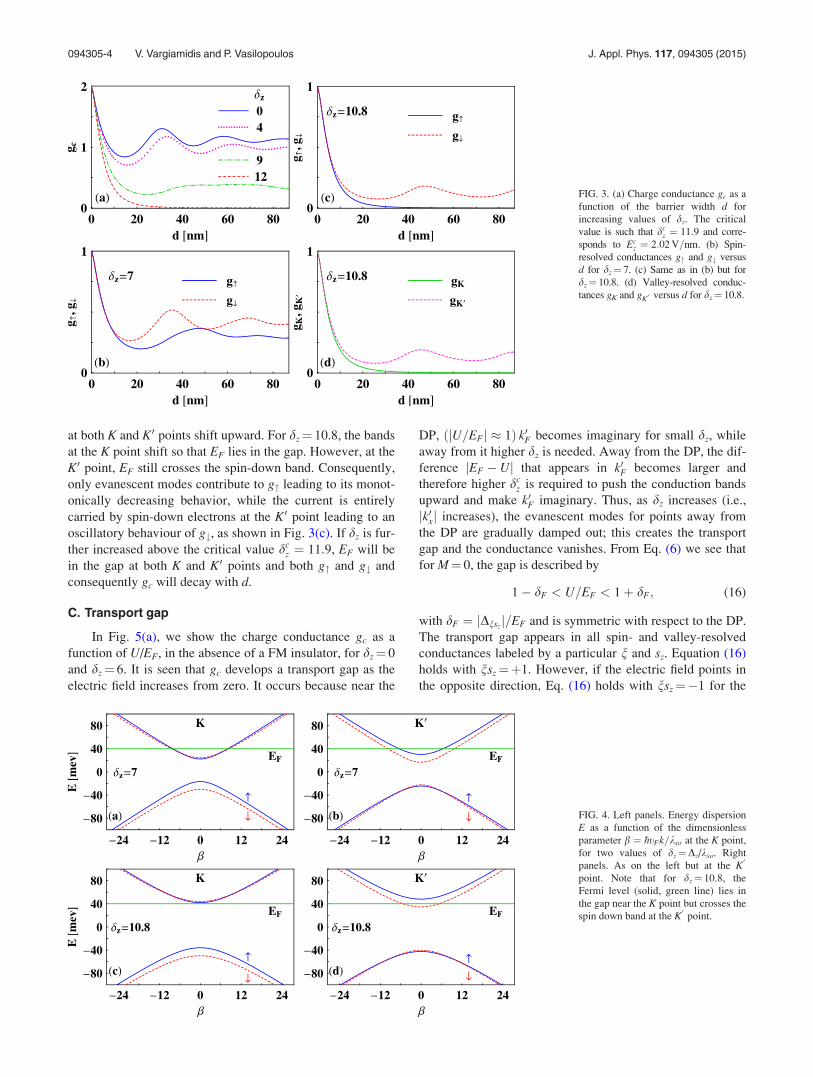
and above Dcz are shown in Fig. 3(a) where we plot gc as a
function of the barrier width d for increasing values of dz. In
general, for each pair (n, sz), there is a separate value of Dz
which yields a decaying behaviour of each Tnsz. However, gc
exhibits a monotonically decaying dependence on d for the
largest value, Dcz , for which all four transmissions Tnsz
exhibit
separately such dependence. For this value, the Fermi level
lies in the gap at both K and K0 points, as discussed in the
context of Fig. 4. We used U/EF¼ 2 and M¼ 2.5 meV which
yield the critical value dcz ¼ Dc
z=kso ¼ 11:9. Note that dz¼ 1
corresponds to Ez¼ 0.17 V/nm. Thus such a junction could
be used as an electric switch. We point out that this effect
has no analogue in graphene. This is due to the fact that in
graphene Dnsz¼ 0 yielding k0F ¼ jEF � Uj=�htF which cannot
be made imaginary. In graphene, k0x becomes purely imagi-
nary only at the DP where k0F ¼ 0.
In Figs. 3(b) and 3(c), we show g" and g# as functions of
d for dz¼ 7 and dz¼ 10.8, respectively. For dz¼ 7, both g"and g# oscillate because the lowest values of dz required for
them to exhibit a decaying behaviour are 10.62 and 11.9,
respectively. However, for dz¼ 10.8, g" exhibits a decaying
behaviour, while g# oscillates. The reason is that for
dz¼ 10.8, EF lies in the gap near the K point while it crosses
the spin-down band at the K0 point, see Fig. 4. This is also
the origin of the large spin polarization discussed in Sec. III.
In Fig. 3(d), we show the valley-resolved conductances, gK
and gK0 , for the same value of dz as in (c). It is seen that they
exhibit a similar behaviour, i.e., gK0 oscillates while gK
decays with d.
The tuning of the charge conductance can be understood
from the band structures at the K and K0 points as dz
increases, see Fig. 4. The upper panels are for dz¼ 7 and the
lower ones for dz¼ 10.8. Also, M¼ 2.5 meV. It can be seen
that as the field Ez increases, the spin-split conduction bands
FIG. 2. Spin-resolved conductances g" and g# through a square barrier
(U� 0) or well (U� 0) as functions of U/EF for dz¼Dz/kso¼ 0 and m¼M/
EF¼ 0. Note that g"¼ g# because the band structures at both K points are the
same in the absence of the FM film.
094305-3 V. Vargiamidis and P. Vasilopoulos J. Appl. Phys. 117, 094305 (2015)
Page 5
at both K and K0 points shift upward. For dz¼ 10.8, the bands
at the K point shift so that EF lies in the gap. However, at the
K0 point, EF still crosses the spin-down band. Consequently,
only evanescent modes contribute to g" leading to its monot-
onically decreasing behavior, while the current is entirely
carried by spin-down electrons at the K0 point leading to an
oscillatory behaviour of g#, as shown in Fig. 3(c). If dz is fur-
ther increased above the critical value dcz ¼ 11:9, EF will be
in the gap at both K and K0 points and both g" and g# and
consequently gc will decay with d.
C. Transport gap
In Fig. 5(a), we show the charge conductance gc as a
function of U/EF, in the absence of a FM insulator, for dz¼ 0
and dz¼ 6. It is seen that gc develops a transport gap as the
electric field increases from zero. It occurs because near the
DP, ðjU=EFj � 1Þ k0F becomes imaginary for small dz, while
away from it higher dz is needed. Away from the DP, the dif-
ference jEF � Uj that appears in k0F becomes larger and
therefore higher dcz is required to push the conduction bands
upward and make k0F imaginary. Thus, as dz increases (i.e.,
jk0xj increases), the evanescent modes for points away from
the DP are gradually damped out; this creates the transport
gap and the conductance vanishes. From Eq. (6) we see that
for M¼ 0, the gap is described by
1� dF < U=EF < 1þ dF; (16)
with dF ¼ jDnszj=EF and is symmetric with respect to the DP.
The transport gap appears in all spin- and valley-resolved
conductances labeled by a particular n and sz. Equation (16)
holds with nsz¼þ1. However, if the electric field points in
the opposite direction, Eq. (16) holds with nsz¼�1 for the
FIG. 3. (a) Charge conductance gc as a
function of the barrier width d for
increasing values of dz. The critical
value is such that dcz ¼ 11:9 and corre-
sponds to Ecz ¼ 2:02 V=nm. (b) Spin-
resolved conductances g" and g# versus
d for dz¼ 7. (c) Same as in (b) but for
dz¼ 10.8. (d) Valley-resolved conduc-
tances gK and gK0 versus d for dz¼ 10.8.
FIG. 4. Left panels. Energy dispersion
E as a function of the dimensionless
parameter b ¼ �htFk=kso at the K point,
for two values of dz¼Dz/kso. Right
panels. As on the left but at the K0
point. Note that for dz¼ 10.8, the
Fermi level (solid, green line) lies in
the gap near the K point but crosses the
spin down band at the K0
point.
094305-4 V. Vargiamidis and P. Vasilopoulos J. Appl. Phys. 117, 094305 (2015)
Page 6
same reasons mentioned in Sec. II B. Note also that for U/EF
¼ 0, i.e., in the absence of a barrier, gc¼ 2 for dz¼ 0.
However, for finite dz (dashed, red curve), there is no perfect
transmission anymore, indicating that the electric field acts
like an extra “barrier” in this region. We also note that a fi-
nite dz causes a shift in the conductance oscillations.
In Fig. 5(b), we show gc as a function of dz for several
values of U/EF close to the DP. Note that near the DP, U/EF
� 1, gc has a monotonically decaying dependence on dz for
dz> 1. This is because the contribution of evanescent modes
gradually diminishes as dz increases, see Eq. (15). However,
for U/EF¼ 1, gc first increases, reaches a maximum at dz¼ 1,
and then decreases. This maximum occurs because jk0Fj at
the DP decreases with dz and vanishes for dz ! 1, resulting
in smaller jk0xj and, consequently, larger contribution of the
evanescent modes.
The effect discussed above can also be observed when
no barrier is present (U¼ 0) by varying EF for fixed, nonzero
dz. In this case, gc becomes finite only beyond a critical
EcF ¼ Dz � kso for which k0F becomes real. For EF < Ec
F,
there are no propagating modes (k0F becomes imaginary) and
the conductance vanishes. This is shown in Fig. 5(c) where
we plot gc as a function of �s¼EF/kso for increasing values
of dz and U¼ 0. As can be seen, below the critical values
�ð1Þs ¼ Ec1
F =kso ¼ 3 and �ð2Þs ¼ Ec2
F =kso ¼ 8, the charge con-
ductance vanishes. We also note that gc¼ 2 when dz¼ 0, as
discussed in Fig. 5(a).
III. INFLUENCE OF THE EXCHANGE FIELD
Below we examine the effects of the exchange field Mon the spin- and valley-resolved conductances. Throughout
this section, we use EF¼ 40 meV and d¼ 110 nm.
A. Spin-resolved conductance
In Fig. 6(a), we show the spin-resolved conductances g",g#, and the charge conductance gc as functions of U/EF for
m¼M/EF¼ 0.058 and dz¼ 0. This value of m corresponds
to exchange splitting M¼ 2.32 meV. As can be seen, the
effect of M is to shift g" and g# relative to each other result-
ing in a broadening of the dip in gc near the DP. Also, the
shift of g" and g# drastically affects gc for high barriers or
deep wells, i.e., for jU=EFj � 1. Specifically, the relative
shift of g" and g# splits each resonance of gc into two spin-
resolved peaks with smaller amplitude, as will be discussed
in the context of Fig. 7(a).
In Fig. 6(b), we show g", g#, and gc as functions of U/EF
for m¼ 0.058 but for finite dz¼ 6. We note that both g" and
g# develop transport gaps which are also shifted relative to
each other, as expected. We also note that the effect of a fi-
nite dz is to shift the oscillations of gc to the right relative to
those for dz¼ 0 while their amplitudes decrease. This is
shown more clearly in Fig. 6(c) where we plot gc versus U/
EF for m¼ 0.058 and the values of dz used in (a) and (b).
The relative shift of the oscillations in g" and g# is
shown in Fig. 6(d) for the same parameter values as in (a). It
is seen that g" and g# can differ substantially at a given value
of U/EF. We also note that all conductances are periodic
functions of U/EF, see explanation below.
Far from the DP, jU=EFj � 1, we obtain an approxi-
mate analytical expression for the spin- and valley-resolved
conductance (see Appendix B)
gnsz’ ½jcj � ð1� c2ÞarctanhðjcjÞ�=jcj cos2x; (17)
with x¼kFdgdk;c¼dkcosx=½1�d2bcos2x�1=2;dk¼½1�ðd2
nsz=
g2Þ�1=2, and d2
b¼d2nsz=g2. The parameter g is given in Eq.
(A1). Equation (17) is in very good agreement with the exact
numerical calculation of gc (see dashed, red line in Fig.
7(a)). From expression (17), we see that gc is periodic in gwith period p/kFddk, which implies that it is a periodic func-
tion of U/EF for fixed M with period Tu ¼ p�htF=EFddk. It is
also periodic in M/EF with the same period. For the parame-
ter values used in this section, we get Tu¼ 0.235.
FIG. 5. (a) Charge conductance gc as a function of U/EF for dz¼ 0 and dz¼ 6.
Note the appearance of a transport gap for dz¼ 6. (b) gc as a function of dz for
three values of the gate voltage near the DP. (c) gc as a function of �s¼EF/kso in
the absence of a barrier (U¼ 0) for increasing values of dz. k0x becomes imaginary
below the critical values �ð1Þs and �
ð2Þs and results in a vanishing conductance.
094305-5 V. Vargiamidis and P. Vasilopoulos J. Appl. Phys. 117, 094305 (2015)
Page 7
In Fig. 7(a), we show gc versus U/EF for dz¼ 0 and sev-
eral values of m. The curves are shifted upward in steps of
0.5. The dashed (red) line is calculated using the approxi-
mate expression (17) for m¼ 0. As can be seen, as mincreases, each peak of gc gradually splits into two spin-
resolved peaks, a distance 2 m apart, of much smaller ampli-
tude. This was also noted in the case of graphene.21 As
shown in Fig. 7(b), by further increasing M, such that
m¼Tu/2, the two spin-resolved peaks merge again to form
one peak of large amplitude as in the case of m¼ 0.
However, the peaks are now shifted by Tu/2 on the U/EF axis
relative to those for m¼ 0. For m¼ 3Tu/4, the peaks resolve
again and become similar to those for m¼ Tu/4 shown in (a).
For m¼Tu, the spin-resolved peaks merge again but are also
shifted by Tu on the U/EF axis, i.e., they coincide with those
for m¼ 0.
In Fig. 7(c), we show gc as a function of m for several
values of U/EF which are close to the first peak in (a). Note
the periodic variation of gc as m increases with period Tu.
We also note that for m¼Tu/2� 0.117, there is a minimum
in gc, whereas, as shown in (b), the two spin-resolved peaks
merge to one of large amplitude. This minimum corresponds
to the first minimum in gc for m¼Tu/2 in (b). Thus, a split-
ting of the conductance peaks occurs at the maxima of gc vs
m. This finding could be useful for the experimental determi-
nation of the exchange field for which proximity-induced
splittings can be observed in ferromagnetic silicene.
B. Valley-resolved conductance
In Fig. 8(a), we show the valley-resolved conductances
gK; gK0 , and the charge conductance gc ¼ gK þ gK0 as func-
tions of U/EF for dz¼ 6 and m¼ 0.04. Contrary to the spin-
resolved conductance, in the barrier (well) region, the field
M splits the resonances of gK and gK0 into spin-resolved
peaks of smaller amplitude. The splitting of the peaks of gK0
in the barrier region is shown more clearly in Fig. 8(d),
where we plot gK and gK0 versus U/EF for the same
parameter values as in (a). This is due to the fact that the val-
ley symmetry is broken when m 6¼ 0, which implies that the
bands at K and K0 points shift in a different way as dz
increases resulting in spin-resolved transport in one valley
but not in the other.
In Fig. 8(b), we show gK; gK0 , and gc as functions of
U/EF for dz¼ 6 and m¼ Tu/4¼ 0.058. In this case, the shift
of gK and gK0 relative to each other is such that it causes
splitting of the peaks of gc, which is similar to that in Fig. 6.
This is shown more clearly in Fig. 8(c) where we plot gc as a
function of U/EF for m¼ 0.04 and Tu/4 corresponding to (a)
and (b).
C. Spin polarization
As usual, the spin polarization ps is defined as
ps ¼ ðg" � g#Þ=ðg" þ g#Þ: (18)
For 0< ps� 1, the transmitted current is spin-up polarized,
while for� 1� ps< 0, its polarization is reversed.
In Fig. 9(a), we show the spin polarization ps as a func-
tion of U/EF for m¼ 0.22 and increasing values of dz. It is
seen that ps becomes more pronounced with increasing dz.
This is mainly due to the fact that the spin-split conduction
bands in the ferromagnetic region shift in a different way at
the K and K0 points with increasing dz, i.e., they shift upward
faster at one valley than at the other one. Thus, for large dz,
only a single spin band contributes to the current giving rise
to large spin polarization. In addition, ps becomes more pro-
nounced because the evanescent modes are gradually sup-
pressed as dz increases. For sufficiently large dz, the charge
current becomes fully spin-polarized with spin-up electrons
below the DP and spin-down electrons above it. The change
of sign in ps is directly related to the relative shift of the con-
ductances g" and g#. Thus, the spin current can be controlled
by the electric field and ps can be inverted by changing the
gate voltage U from negative to positive.
FIG. 6. (a) Spin-resolved conductances
g" and g#, and charge conductance
gc¼ g"þ g# as functions of U/EF for
dz¼ 0 and m¼ 0.058. (b) The same as
in (a) but for dz¼ 6. (c) gc as a function
of U/EF for m¼ 0.058, and the values
of dz used in (a) and (b). (d) g" and g#as functions of U/EF for the same pa-
rameters as in (a).
094305-6 V. Vargiamidis and P. Vasilopoulos J. Appl. Phys. 117, 094305 (2015)
Page 8
The spin polarization can also be controlled by varying
the exchange field. This is shown in Fig. 9(b) where we plot
ps versus of U/EF for dz¼ 5 and increasing values of m. As
in (a), fully spin-polarized current can be achieved for suffi-
ciently large m, which is a consequence of the broken valley
symmetry. In passing, we note that ps becomes more pro-
nounced with increasing width d.26
The spin polarization can also be tuned by changing the
direction of the exchange field from positive to negative.
This is shown in Fig. 10(a) where we plot ps as a function of
U/EF for dz¼ 8 and m¼60.22. As can be seen, ps is
inverted by simply reversing the direction of the exchange
field. For m¼ 0.22, the transmitted current is spin-up (spin-
down) polarized below (above) the DP, while for m¼�0.22,
it becomes spin-down (spin-up) polarized. In Fig. 10(b), we
show the valley polarization pv ¼ ðgK � gK0 Þ=ðgK þ gK0 Þ as
a function of U/EF for the same parameter values as in (a). It
is seen that the sign of pv can also be switched by reversing
the direction of m. However, the regions of near-perfect val-
ley polarization are shorter than those of ps. In Fig. 10(c), we
show ps as a function of m for U/EF¼61.7 and dz¼ 8. It is
seen that as m changes sign, the spin polarization also
changes sign. Above (below) the DP (U/EF¼61.7), ps
becomes negative (positive) as m becomes positive. As men-
tioned above, this is directly related to the relative shift of
the conductances g" and g#. This is shown in Figs. 10(d) and
10(e), where we plot g" and g#, as functions of U/EF, for
m¼ 0.06 and �0.06, respectively. For m¼�0.06, the shift
of g" and g# relative to each other is opposite to that for
m¼ 0.06. As a result, the sign of ps changes when m is
reversed. Similar considerations hold for pv. These findings
could be used to realize a silicene-based, high-efficiency
spin- and valley-filter.
IV. DOUBLE FERROMAGNETIC JUNCTION
In this section, we study a double ferromagnetic junction
shown schematically in Fig. 1(b). The magnetic gates, both
of width d and a distance b apart, extend over regions II and
IV, We assume that Ez is applied only in these regions and
vanishes everywhere else.
The eigenfunctions are of the same form as those for a
single ferromagnetic junction (see Sec. II A). In regions I,
III, and V, kF is given by Eq. (5) and kðiÞF in regions II and IV
by Eq. (6) with k0F ! kðiÞF . Also, similar to Eq. (7), we now
have ky ¼ kðiÞy ) kF sin h ¼ k
ðiÞF sin /i; i ¼ II, IV, where
h ¼ arctanðky=kxÞ is the angle that the incident particle makes
with the x axis, and /i ¼ arctanðkðiÞy =kðiÞx Þ the angle inside the
first or second barrier. Applying the continuity of the wave
function at the interfaces leads to a system of eight equations
with eight unknowns which are solved numerically to obtain
the transmission. We also defined the longitudinal momenta
as in Eq. (9), that is, kðiÞx ¼ ½ðkðiÞF Þ
2 � k2F sin2h�1=2; i ¼ II, IV.
In the numerical calculation, we used d¼ 100 nm, b¼ 50 nm,
and EF¼ 40 meV. We also set dz ¼ dð1Þz ¼ dð2Þz the common
value of the electric field in the two regions.
In Fig. 11, we show the charge conductance gc as a func-
tion of the barrier width d for increasing values of dz. We
used U1/EF¼ 2, U2¼U1, and the same exchange fields
mi¼Mi/EF¼ 0.063, i¼ 1, 2. We find that gc decays expo-
nentially with d beyond a critical value of dz, as in the case
of a single barrier. In fact, the expression for the critical dcz is
the same as that for a single barrier. We note that it is suffi-
cient to increase either dð1Þz or dð2Þz above dcz in order to
observe the exponentially decaying behaviour of gc. For the
parameters used here, the critical value is dcz ¼ 11:9, the
same as for a single barrier. We also note that a near-zero
transmission is achieved faster because the two barriers to-
gether increase the effective width. Below dcz ¼ 11:9, gc
remains oscillatory; however, the oscillation patterns are
more complex.
In Fig. 12(a), we show g" as a function of V/EF for two
values of dz. We take U1¼U2¼V, i.e., the barriers have
equal heights, and vanishing exchange fields, m1¼m2¼ 0.
In this case, g#¼ g". We note that for dz¼ 0, g" is almost
FIG. 7. (a) Charge conductance gc versus U/EF for dz¼ 0 and several values
of the exchange field m. The curves are shifted upward in steps of 0.5. The
dashed (red) curve is computed using the approximate expression (17). (b)
gc versus U/EF for m¼ 0 and Tu/2. (c) gc versus m for three values of U/EF
close to the first peak in (a).
094305-7 V. Vargiamidis and P. Vasilopoulos J. Appl. Phys. 117, 094305 (2015)
Page 9
zero at V/EF� 1. This occurs because the two barriers to-
gether increase the effective width which causes a drastic
suppression of transport through the evanescent modes.
Also, increasing dz from zero leads to a transport gap similar
to that for a single barrier. It has the same form as that for a
single barrier and be found from an equation similar to Eq.
(16) with the change k0F ! kðiÞF . We also note that the oscilla-
tory pattern is the same as that for a single barrier but, for
dz¼ 0, it becomes slightly irregular in the barrier region.
In Fig. 12(b), we show the charge conductance gc as a
function of �s¼EF/kso for V¼ 0, vanishing exchange fields
m1¼m2¼ 0, and increasing values of dz. We note that gc¼ 2
for dz¼ 0, as expected. We also note that gc vanishes below
a critical value of the Fermi energy, i.e., for �s < EcF=kso
where EcF ¼ Dz � kso, for which k
ðiÞF becomes imaginary, as
in the case of a single barrier.
For barriers (wells) of unequal height (depth), the con-
ductance has a richer structure. In Fig. 12(c), we show g"as a function of V/EF for U1¼V with U2¼ 1.2 V (solid,
blue curve) and U2¼ 0.8 V (dashed, red curve). The elec-
tric and exchange fields are taken to be zero. First, it is
seen that the dips are broadened and shift away from the
DP. Second, the oscillation pattern in the barrier region
becomes more complex and irregular. We also observe a
beating pattern with progressively larger oscillations with
increasing depth of the wells. We attribute the beating to
the interference of Dirac fermions with slightly different
energy due to the asymmetry of the two wells. This pattern
is similar to that found for asymmetric electrostatic wells
in graphene.31
In Fig. 12(d), we show g", g#, and gc as functions of V/
EF for U2¼ 1.2U1. The electric and exchange fields are such
that dz¼ 6 and m1¼m2¼ 0.05. It is seen that both g" and g#exhibit beating patterns in the well region. Also, the relative
shift of g" and g# leads to irregular oscillations of gc, espe-
cially in the barrier region, which cannot be used to deter-
mine the exchange splittings.
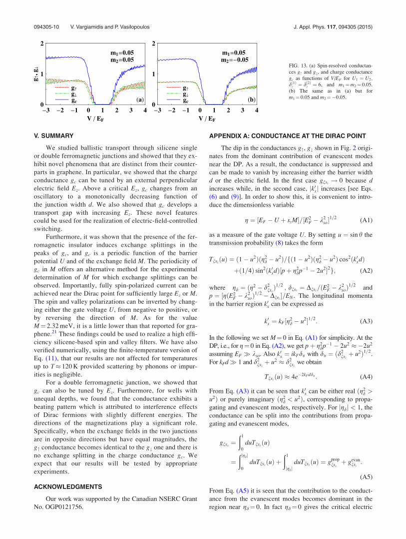
We demonstrate now the effect of the exchange fields
on the spin-resolved and charge conductances. In Fig. 13(a),
we show g", g#, and gc as functions of V/EF for dz ¼ dð1Þz
¼ dð2Þz ¼ 6; m1 ¼ m2 ¼ 0:05, and for barriers of equal height
U1¼U2¼V. As can be seen, the exchange fields shift g"and g# relative to each other resulting in splitting of the
peaks in the charge conductance, as in the case of a single
barrier. However, the amplitudes of the oscillations in g"and g# become much larger than those for a single barrier
FIG. 8. (a) Valley-resolved conductan-
ces gK and gK0 , and charge conduct-
ance gc as functions of U/EF for dz¼ 6
and m¼ 0.04. (b) The same as in (a)
but for m¼Tu/4. (c) gc vs U/EF for
dz¼ 6 and the values of m used in (a)
and (b). (d) Valley-resolved conduc-
tances gK, gK0 , as functions of U/EF for
the same parameters as in (a).
FIG. 9. (a) Spin polarization ps as a function of U/EF for m¼ 0.22 and
increasing values of dz. (b) The same as in (a) but for fixed dz¼ 5 and several
values of m.
094305-8 V. Vargiamidis and P. Vasilopoulos J. Appl. Phys. 117, 094305 (2015)
Page 10
(see Fig. 6(b)). This is also reflected in the oscillations of gc
which are also slightly irregular.
In Fig. 13(b), we show g", g#, and gc as functions of V/
EF with the exchange fields in opposite directions, m1¼ 0.05
and m2¼� 0.05. Interestingly, we find that g" becomes iden-
tical to g#, i.e., the exchange fields do not shift g" and g# rela-
tive to each other. It is as if the exchange fields have
opposite effects. This is due to the particular combination of
Mi and sz which enters the wave vectors kðiÞF . Specifically, the
effect of a positive Mi on spin-up electrons is identical to
that of a negative Mi on spin-down electrons, i.e., szMi is pos-
itive in both cases. This explains the equality g"¼ g# and the
absence of splitting in gc. The absence of splittings leads to
zero spin polarization through the double junction. At the
same time, we note that the amplitudes of the oscillations in
g" and g# are strongly suppressed.
FIG. 10. (a) Spin polarization ps as a
function of U/EF for dz¼ 8 and
m¼60.22. Note that ps is inverted
when the direction of the exchange
field is reversed. (b) The same as in (a)
but for the valley polarization pv. (c)
Spin polarization ps as a function of mfor U/EF¼61.7. (d) Conductances g"and g# as functions of U/EF for
m¼60.06.
FIG. 11. Charge conductance gc as a function of the barrier width d for
increasing values of dz. The critical value is dcz ¼ 11:9 and m1¼m2¼ 0.063.
FIG. 12. (a) Spin-up conductance g" as
a function of V/EF with U1¼U2¼Vand m1¼m2¼ 0. (b) Charge conduct-
ance gc as a function of �s¼EF/kso for
V¼ 0 and increasing values of dz. (c)
g" versus V/EF for U1¼V, two values
of U2/U1, and dz¼m¼ 0. (d)
Conductances g", g#, and gc versus V/
EF for dz¼ 6 and m1¼m2¼ 0.05.
094305-9 V. Vargiamidis and P. Vasilopoulos J. Appl. Phys. 117, 094305 (2015)
Page 11
V. SUMMARY
We studied ballistic transport through silicene single
or double ferromagnetic junctions and showed that they ex-
hibit novel phenomena that are distinct from their counter-
parts in graphene. In particular, we showed that the charge
conductance gc can be tuned by an external perpendicular
electric field Ez. Above a critical Ez, gc changes from an
oscillatory to a monotonically decreasing function of
the junction width d. We also showed that gc develops a
transport gap with increasing Ez. These novel features
could be used for the realization of electric-field-controlled
switching.
Furthermore, it was shown that the presence of the fer-
romagnetic insulator induces exchange splittings in the
peaks of gc, and gc is a periodic function of the barrier
potential U and of the exchange field M. The periodicity of
gc in M offers an alternative method for the experimental
determination of M for which exchange splittings can be
observed. Importantly, fully spin-polarized current can be
achieved near the Dirac point for sufficiently large Ez or M.
The spin and valley polarizations can be inverted by chang-
ing either the gate voltage U, from negative to positive, or
by reversing the direction of M. As for the value
M¼ 2.32 meV, it is a little lower than that reported for gra-
phene.21 These findings could be used to realize a high effi-
ciency silicene-based spin and valley filters. We have also
verified numerically, using the finite-temperature version of
Eq. (11), that our results are not affected for temperatures
up to T� 120 K provided scattering by phonons or impur-
ities is negligible.
For a double ferromagnetic junction, we showed that
gc can also be tuned by Ez. Furthermore, for wells with
unequal depths, we found that the conductance exhibits a
beating pattern which is attributed to interference effects
of Dirac fermions with slightly different energies. The
directions of the magnetizations play a significant role.
Specifically, when the exchange fields in the two junctions
are in opposite directions but have equal magnitudes, the
g" conductance becomes identical to the g# one and there is
no exchange splitting in the charge conductance gc. We
expect that our results will be tested by appropriate
experiments.
ACKNOWLEDGMENTS
Our work was supported by the Canadian NSERC Grant
No. OGP0121756.
APPENDIX A: CONDUCTANCE AT THE DIRAC POINT
The dip in the conductances g", g# shown in Fig. 2 origi-
nates from the dominant contribution of evanescent modes
near the DP. As a result, the conductance is suppressed and
can be made to vanish by increasing either the barrier width
d or the electric field. In the first case gnsz! 0 because d
increases while, in the second case, jk0xj increases [see Eqs.
(6) and (9)]. In order to show this, it is convenient to intro-
duce the dimensionless variable
g ¼ ½EF � U þ szM�=½E2F � k2
so�1=2
(A1)
as a measure of the gate voltage U. By setting u ¼ sin h the
transmission probability (8) takes the form
TnszðuÞ ¼ ð1� u2Þðg2
d � u2Þ=fð1� u2Þðg2d � u2Þ cos2ðk0xdÞ
þð1=4Þ sin2ðk0xdÞ½pþ g2dp�1 � 2u2�2g; (A2)
where gd ¼ ðg2 � d2nszÞ1=2 ; dnsz
¼ Dnsz=ðE2
F � k2soÞ
1=2and
p ¼ ½gðE2F � k2
soÞ1=2 � Dnsz
�=EN . The longitudinal momenta
in the barrier region k0x can be expressed as
k0x ¼ kF½g2d � u2�1=2: (A3)
In the following we set M¼ 0 in Eq. (A1) for simplicity. At the
DP, i.e., for g¼ 0 in Eq. (A2), we get pþ g2dp�1 � 2u2 � �2u2
assuming EF� kso. Also k0x ¼ ikFda with da ¼ ðd2nszþ u2Þ1=2
.
For kFd� 1 and d2nszþ u2 � d2
nszwe obtain
TnszðuÞ � 4e�2kFdda : (A4)
From Eq. (A3) it can be seen that k0x can be either real ðg2d >
u2Þ or purely imaginary ðg2d < u2Þ, corresponding to propa-
gating and evanescent modes, respectively. For jgdj < 1, the
conductance can be split into the contributions from propa-
gating and evanescent modes,
gnsz¼ð1
0
duTnszðuÞ
¼ðjgdj
0
duTnszðuÞ þ
ð1
jgdjduTnsz
ðuÞ ¼ gpropnszþ gevan
nsz:
(A5)
From Eq. (A5) it is seen that the contribution to the conduct-
ance from the evanescent modes becomes dominant in the
region near gd¼ 0. In fact gd¼ 0 gives the critical electric
FIG. 13. (a) Spin-resolved conductan-
ces g" and g#, and charge conductance
gc as functions of V/EF for U1 ¼ U2;dð1Þz ¼ dð2Þz ¼ 6, and m1¼m2¼ 0.05.
(b) The same as in (a) but for
m1¼ 0.05 and m2¼�0.05.
094305-10 V. Vargiamidis and P. Vasilopoulos J. Appl. Phys. 117, 094305 (2015)
Page 12
field Dcz ¼ nszkso6jEF � U þ szMj mentioned in Sec. II B.
Inserting Eq. (A4) into Eq. (A5) and using da � jdnszj þ u2=
2jdnszj we find
gnsz� ð4p=qÞ1=2e�2kFdjdnsz jerfð ffiffiffiqp Þ; (A6)
where q ¼ kFd=jdnszj; erf(x) is the error function. Equation
(A6) is in very good agreement with the exact numerical cal-
culation presented in Fig. 4(b) as long as dnsz Dnsz
6¼ 0. It
can be seen that, for any spin or valley index, gnszexhibits a
monotonically decaying dependence on dz as long as dz> 1.
It also exhibits a similar dependence on the width d of the
barrier for fixed dz.
APPENDIX B: CONDUCTANCE FOR STRONGPOTENTIALS
For high barriers or deep wells, jgj � 1, using u2� 1 we
have u2/g2! 0. Also in Eq. (A2) we have
pþ g2dp�1 � u2 ’ 2g; (B1)
where we assumed that EF � kso. Also k0xd ’ kFdgdk with
dk ¼ ½1� ðd2nsz=g2Þ�1=2
. Then, with d2b ¼ d2
nsz=g2 and x¼ kF
dgdk, Eq. (A2) takes the form
Tnszuð Þ ’
1� d2b þ u2 � d2
bu2� �
1� d2b þ u2 � d2
bu2� �
cos2x: (B2)
Inserting Eq. (B2) in Eq. (A5) we get
gnsz’ jcj � 1� c2
� �arctanh jcjð Þ
jcj cos2x; (B3)
where c ¼ dk cos x=½1� d2b cos2x�1=2
. We notice that this
gnszis periodic in the variable g with period p/kFddk.
Equation (B3) is in very good agreement with the exact nu-
merical calculation for either zero or finite dz and M.
1G. G. Guzm�an-Verri and L. C. Lew Yan Voon, Phys. Rev. B 76, 075131
(2007); S. Lebegue and O. Eriksson, Phys. Rev. B 79, 115409 (2009).2P. Vogt, P. De Padova, C. Quaresima, J. Avila, E. Frantzeskakis, M. C.
Asensio, A. Resta, B. Ealet, and G. Le Lay, Phys. Rev. Lett. 108, 155501
(2012); A. Fleurence, R. Friedlein, T. Ozaki, H. Kawai, Y. Wang, and Y.
Yamada-Takamura, ibid. 108, 245501 (2012).3D. Chiappe, E. Scalise, E. Cinquanta, C. Grazianetti, B. V. Broek, M.
Fanciulli, M. Houssa, and A. Molle, Adv. Mater. 26, 2096 (2014).4Z. Ni, Q. Liu, K. Tang, J. Zheng, J. Zhou, R. Qin, Z. Gao, D. Yu, and J.
Lu, Nano Lett. 12, 113 (2012); Y. Cai, C.-P. Chuu, C. M. Wei, and M. Y.
Chou, Phys. Rev. B 88, 245408 (2013); M. Neek-Amal, A. Sadeghi, G. R.
Berdiyorov, and F. M. Peeters, Appl. Phys. Lett. 103, 261904 (2013); H.
Liu, J. Gao, and J. Zhao, J. Phys. Chem. C 117, 10353 (2013).5A. H. Castro Neto, F. Guinea, N. M. R. Peres, K. S. Novoselov, and A. K.
Geim, Rev. Mod. Phys. 81, 109 (2009).6C.-C. Liu, W. Feng, and Y. Yao, Phys. Rev. Lett. 107, 076802
(2011).7N. D. Drummond, V. Z�olyomi, and V. I. F’alko, Phys. Rev. B 85, 075423
(2012).8M. Ezawa, New J. Phys. 14, 033003 (2012).9A. Dyrdał and J. Barnas, Phys. Status Solidi RRL 6, 340 (2012).
10M. Tahir, A. Manchon, K. Sabeeh, and U. Schwingenschl€ogl, Appl. Phys.
Lett. 102, 162412 (2013).11C. J. Tabert and E. J. Nicol, Phys. Rev. B 87, 235426 (2013).12X.-T. An, Y.-Y. Zhang, J.-J. Liu, and S.-S. Li, Appl. Phys. Lett. 102,
043113 (2013).13M. Ezawa, Phys. Rev. Lett. 109, 055502 (2012).14L. Stille, C. J. Tabert, and E. J. Nicol, Phys. Rev. B 86, 195405
(2012).15A. Kara, H. Enriquez, A. P. Seitsonen, L. C. Lew Yan Voon, S. Vizzini, B.
Aufray, and H. Oughaddoub, Surf. Sci. 67, 1 (2012).16C.-C. Liu, H. Jiang, and Y. Yao, Phys. Rev. B 84, 195430 (2011).17B. Huang, D. J. Monsma, and I. Appelbaum, Phys. Rev. Lett. 99, 177209
(2007).18Y. Wang, J. Zheng, Z. Ni, R. Fei, Q. Liu, R. Quhe, C. Xu, J. Zhou, Z. Gao,
and J. Lu, Nano 7, 1250037 (2012).19S. Sanvito, Chem. Soc. Rev. 40, 3336 (2011).20N. Tombros, C. Jozsa, M. Popinciuc, H. T. Jonkman, and B. J. van Wees,
Nature 448, 571 (2007).21H. Haugen, D. Huertas-Hernando, and A. Brataas, Phys. Rev. B 77,
115406 (2008).22J. Milton Pereira, Jr., P. Vasilopoulos, and F. M. Peeters, Appl. Phys. Lett.
90, 132122 (2007).23T. Yokoyama, Y. Tanaka, and N. Nagaosa, Phys. Rev. B 81, 121401(R)
(2010).24H. Pan, Z. Li, C.-C. Liu, G. Zhu, Z. Qiao, and Y. Yao, Phys. Rev Lett.
112, 106802 (2014).25S. Mondal, D. Sen, K. Sengupta, and R. Shankar, Phys. Rev. Lett. 104,
046403 (2010).26T. Yokoyama, Phys. Rev. B 87, 241409(R) (2013).27B. Soodchomshom, J. Appl. Phys. 115, 023706 (2014).28M. Ezawa, Phys. Rev. B 87, 155415 (2013).29V. Vargiamidis and P. Vasilopoulos, Appl. Phys. Lett. 105, 223105
(2014).30P. G. Silvestrov and K. B. Efetov, Phys. Rev. Lett. 98, 016802
(2007).31L. Liu, Y.-X. Li, Y.-T. Zhang, and J.-J. Liu, J. Appl. Phys. 115, 023704
(2014).
094305-11 V. Vargiamidis and P. Vasilopoulos J. Appl. Phys. 117, 094305 (2015)