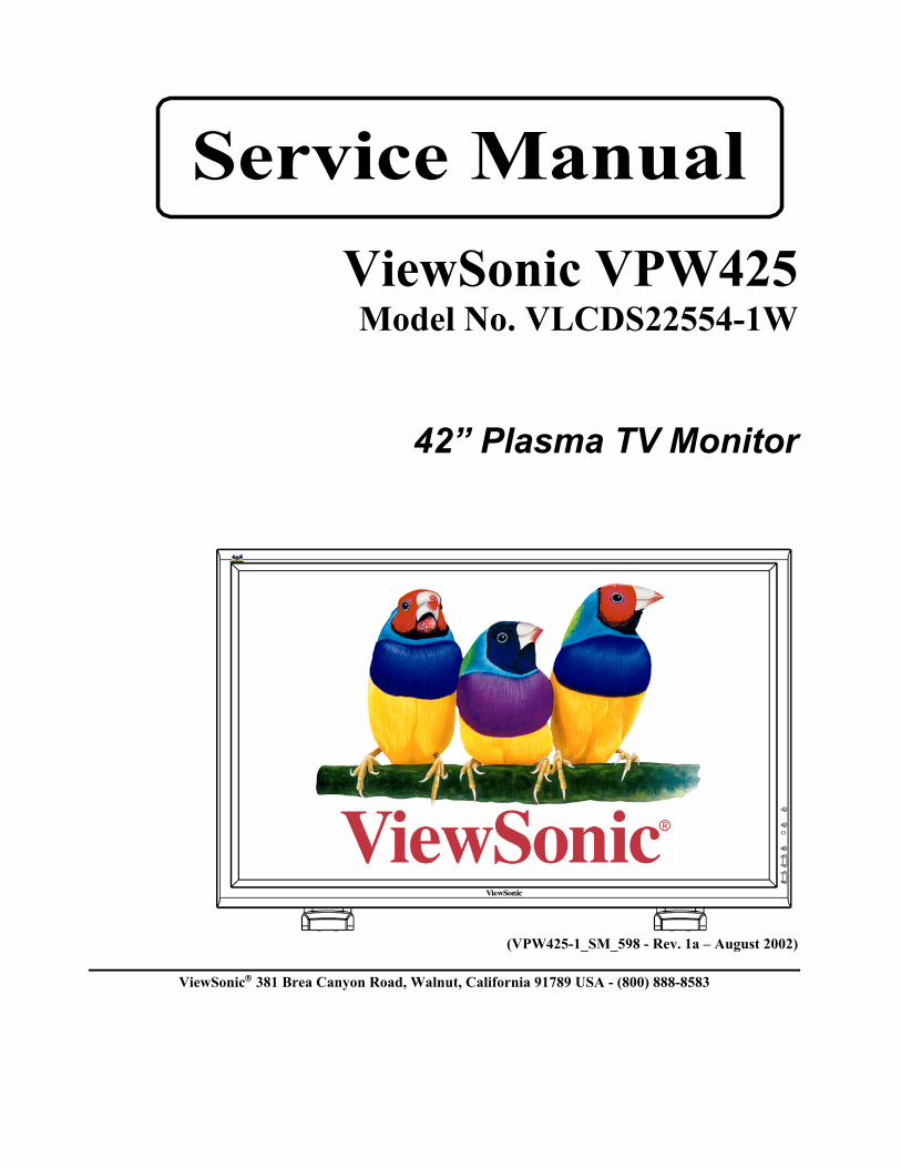
Service Manual ViewSonic VPW425 Model No. VLCDS22554-1W 42” Plasma TV Monitor (VPW425-1_SM_598 - Rev. 1a – August 2002) ViewSonic 381 Brea Canyon Road, Walnut, California 91789 USA - (800) 888-8583
Transcript
Service ManualViewSonic VPW425Model No. VLCDS22554-1W
42” Plasma TV Monitor
(VPW425-1_SM_598 - Rev. 1a – August 2002)
ViewSonic 381 Brea Canyon Road, Walnut, California 91789 USA - (800) 888-8583
ii VPW425-1 Service Manual
Copyright
Copyright 2002 by ViewSonic Corporation. All rights reserved. No part of this publication may bereproduced, transmitted, transcribed, stored in a retrieval system, or translated into any language orcomputer language, in any form or by any means, electronic, mechanical, magnetic, optical, chemical,manual or otherwise, without the prior written permission of ViewSonic Corporation.
Disclaimer
ViewSonic makes no representations or warranties, either expressed or implied, with respect to thecontents hereof and specifically disclaims any warranty of merchantability or fitness for any particularpurpose. Further, ViewSonic reserves the right to revise this publication and to make changes from timeto time in the contents hereof without obligation of ViewSonic to notify any person of such revision orchanges.
Trademarks
ViewSonic is a registered trademark of ViewSonic Corporation.All other trademarks used within this document are the property of their respective owners.
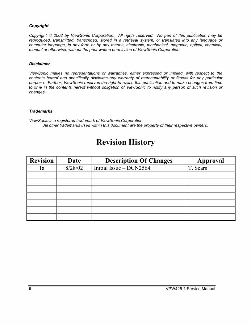
Revision History
Revision Date Description Of Changes Approval1a 8/28/02 Initial Issue – DCN2564 T. Sears
Service ManualViewSonic VPW425Model No. VLCDS22554-1W
42” Plasma TV Monitor
(VPW425-1_SM_598 - Rev. 1a – August 2002)
ViewSonic 381 Brea Canyon Road, Walnut, California 91789 USA - (800) 888-8583
ii VPW425-1 Service Manual
Copyright
Copyright 2002 by ViewSonic Corporation. All rights reserved. No part of this publication may bereproduced, transmitted, transcribed, stored in a retrieval system, or translated into any language orcomputer language, in any form or by any means, electronic, mechanical, magnetic, optical, chemical,manual or otherwise, without the prior written permission of ViewSonic Corporation.
Disclaimer
ViewSonic makes no representations or warranties, either expressed or implied, with respect to thecontents hereof and specifically disclaims any warranty of merchantability or fitness for any particularpurpose. Further, ViewSonic reserves the right to revise this publication and to make changes from timeto time in the contents hereof without obligation of ViewSonic to notify any person of such revision orchanges.
Trademarks
ViewSonic is a registered trademark of ViewSonic Corporation.All other trademarks used within this document are the property of their respective owners.
Revision History
Revision Date Description Of Changes Approval1a 8/28/02 Initial Issue – DCN2564 T. Sears
1. Before returning an instrument to the customer, always make a safety check of the entire instrument,including, but not limited to, the following items.
a. Be sure that no built-in protective devices are defective and/or have been defeated during servicing. (1) Protectiveshields are provided on this chassis to protect both the technician and the customer. Correctly replace all missingprotective shields, including any removed for servicing convenience. (2) When reinstalling the chassis and/orother assembly in the cabinet, be sure to put back in place all protective devices, including, but not limited to,nonmetallic control knobs, insulating fishpapers, adjustment and compartment covers/shields, and isolationresistor/capacitor networks. Do not operate this instrument or permit it to be operated without all protectivedevices correctly installed and functioning.
b. Be sure that there are no cabinet openings through which an adult or child might be able to insert their fingersand contact a hazardous voltage, Such opening include, but are not limited to, (1) spacing between the picturetube and the cabinet mask, (2) excessively wide cabinet ventilation slots, and (3) an improperly fitted and/orincorrectly secured cabinet back cover.
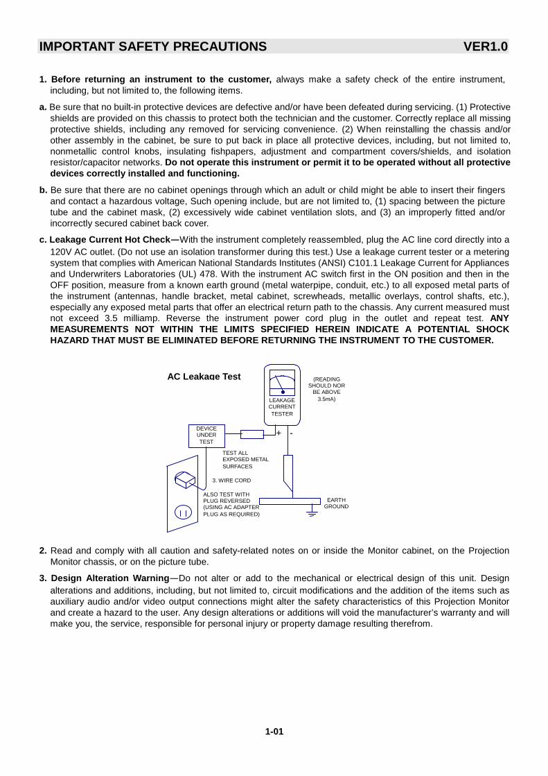
c. Leakage Current Hot Check————With the instrument completely reassembled, plug the AC line cord directly into a120V AC outlet. (Do not use an isolation transformer during this test.) Use a leakage current tester or a meteringsystem that complies with American National Standards Institutes (ANSI) C101.1 Leakage Current for Appliancesand Underwriters Laboratories (UL) 478. With the instrument AC switch first in the ON position and then in theOFF position, measure from a known earth ground (metal waterpipe, conduit, etc.) to all exposed metal parts ofthe instrument (antennas, handle bracket, metal cabinet, screwheads, metallic overlays, control shafts, etc.),especially any exposed metal parts that offer an electrical return path to the chassis. Any current measured mustnot exceed 3.5 milliamp. Reverse the instrument power cord plug in the outlet and repeat test. ANYMEASUREMENTS NOT WITHIN THE LIMITS SPECIFIED HEREIN INDICATE A POTENTIAL SHOCKHAZARD THAT MUST BE ELIMINATED BEFORE RETURNING THE INSTRUMENT TO THE CUSTOMER.
2. Read and comply with all caution and safety-related notes on or inside the Monitor cabinet, on the ProjectionMonitor chassis, or on the picture tube.
3. Design Alteration Warning————Do not alter or add to the mechanical or electrical design of this unit. Designalterations and additions, including, but not limited to, circuit modifications and the addition of the items such asauxiliary audio and/or video output connections might alter the safety characteristics of this Projection Monitorand create a hazard to the user. Any design alterations or additions will void the manufacturer’s warranty and willmake you, the service, responsible for personal injury or property damage resulting therefrom.
DEVICEUNDERTEST
ALSO TEST WITHPLUG REVERSED(USING AC ADAPTERPLUG AS REQUIRED)
TEST ALLEXPOSED METALSURFACES
LEAKAGECURRENTTESTER
+ -
EARTHGROUND
3. WIRE CORD
AC Leakage Test (READINGSHOULD NOR
BE ABOVE3.5mA)
IMPORTANT SAFETY PRECAUTIONS VER1.0
1-02
4. Hot Chassis Warning————a. Some Monitor chassis are electrically connected directly to one conductor of the ACpower cord and may be safely serviced without an isolation transformer only if the AC power plug is inserted sothat the chassis is connected to the ground side of the AC power source. To confirm that the AC power plug isinserted correctly, with an AC voltmeter measure between the chassis and a known earth ground. If a voltagereading in excess of 1.0V is obtained, remove and reinsert the AC power plug in opposite polarity and againmeasure the voltage potential between the chassis and a known earth ground. b. Some Monitor chassis normallyhave 85V AC (RMS.), between chassis and earth ground regardless of the AC plug polarity. These chassis canbe safely serviced only with an isolation transformer inserted in the power line between the receiver and the ACpower source, for both personnel and test equipment protection. c. Some Projection Monitor chassis have asecondary ground systems in addition to the main chassis ground. This secondary ground system is not isolatedfrom the AC power line. The two ground system are electrically separated by insulating material that must not bedefeated or altered.
5. Observe original lead dress. Take extra care to assure correct lead dress in the following areas: a. near sharpedges, b. near thermally hot parts—be sure that leads and components do not touch thermally hot parts, c. theAC supply, d. high voltage, e. antenna wiring. Always inspect in all areas for pinched, out-of-place, or frayedwiring. Do not change spacing between components, and between components and the printed-circuit board.Check AC power cord for damage.
6. Components, parts, and/or wiring that appear to have overheated or are otherwise damaged should be replacedwith components, parts, or wireing that meet original specifications. Additionally, determine the cause ofoverheating and/or damage and, if necessary, take corrective action to remove any potential safety hazard.
7. PRODUCT SAFETY NOTICE————Many Monitor electrical and mechanical parts have special safety-relatedcharacteristics some of which are often not evident from visual inspection, nor can the protection they givenecessarily be obtained by replacing them with components rated for higher voltage, wattage, etc. Parts that havespecial safety characteristics are identified in this service data by shading with a mark on schematics and byshading or a * mark in the parts list. Use of a substitute replacement part that does not have the same safetycharacteristics as the recommended replacement part in this service data parts list might create shock, fire,and/or other hazards.
SPECIFICATION VER1.0
2-1
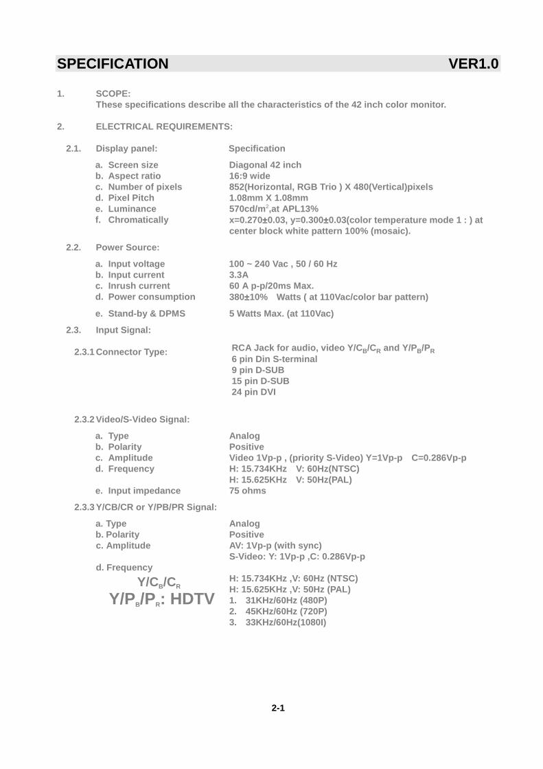
1. SCOPE:These specifications describe all the characteristics of the 42 inch color monitor.
2. ELECTRICAL REQUIREMENTS:
2.1. Display panel: Specification
a. Screen size Diagonal 42 inchb. Aspect ratio 16:9 widec. Number of pixels 852(Horizontal, RGB Trio ) X 480(Vertical)pixelsd. Pixel Pitch 1.08mm X 1.08mme. Luminance 570cd/m2,at APL13%f. Chromatically x=0.270±±±±0.03, y=0.300±±±±0.03(color temperature mode 1 : ) at
center block white pattern 100% (mosaic).
2.2. Power Source:
a. Input voltage 100 ~ 240 Vac , 50 / 60 Hzb. Input current 3.3Ac. Inrush current 60 A p-p/20ms Max.d. Power consumption 380±±±±10% Watts ( at 110Vac/color bar pattern)
e. Stand-by & DPMS 5 Watts Max. (at 110Vac)
2.3. Input Signal:
2.3.1 Connector Type: RCA Jack for audio, video Y/CB/CR and Y/PB/PR
6 pin Din S-terminal9 pin D-SUB15 pin D-SUB24 pin DVI
2.3.2 Video/S-Video Signal:
a. Type Analogb. Polarity Positivec. Amplituded. Frequency
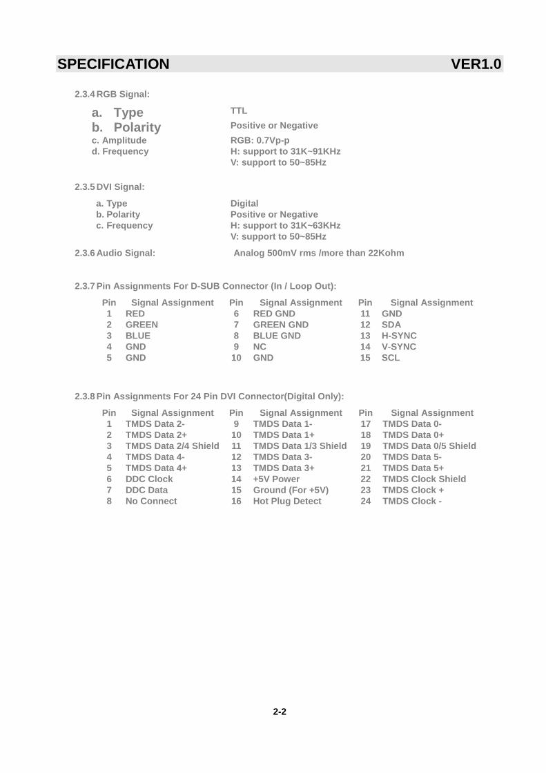
c. Amplitude RGB: 0.7Vp-pd. Frequency H: support to 31K~91KHz
V: support to 50~85Hz
2.3.5 DVI Signal:
a. Typeb. Polarityc. Frequency
DigitalPositive or NegativeH: support to 31K~63KHzV: support to 50~85Hz
2.3.6 Audio Signal: Analog 500mV rms /more than 22Kohm
2.3.7 Pin Assignments For D-SUB Connector (In / Loop Out):
Pin Signal Assignment Pin Signal Assignment Pin Signal Assignment1 RED 6 RED GND 11 GND2 GREEN 7 GREEN GND 12 SDA3 BLUE 8 BLUE GND 13 H-SYNC4 GND 9 NC 14 V-SYNC5 GND 10 GND 15 SCL
2.3.8 Pin Assignments For 24 Pin DVI Connector(Digital Only):
Pin Signal Assignment Pin Signal Assignment Pin Signal Assignment1 TMDS Data 2- 9 TMDS Data 1- 17 TMDS Data 0-2 TMDS Data 2+ 10 TMDS Data 1+ 18 TMDS Data 0+3 TMDS Data 2/4 Shield 11 TMDS Data 1/3 Shield 19 TMDS Data 0/5 Shield4 TMDS Data 4- 12 TMDS Data 3- 20 TMDS Data 5-5 TMDS Data 4+ 13 TMDS Data 3+ 21 TMDS Data 5+6 DDC Clock 14 +5V Power 22 TMDS Clock Shield7 DDC Data 15 Ground (For +5V) 23 TMDS Clock +8 No Connect 16 Hot Plug Detect 24 TMDS Clock -
2.4. Display Performance Requirements:The data of display performance are measured based on the following.Conditions unless otherwise specified.
a. Ambient temperature 25±±±±5 ℃℃℃℃b. Warm up period 30 minutes Min.c. Line input voltage : 100 Vac ~ 240 Vac (50 / 60 Hz)d. Viewing distance Distance from screen is 81 cme. Display mode Test with window white pattern mode if not specified.f. Brightness condition Press recall bottom to set default brightness
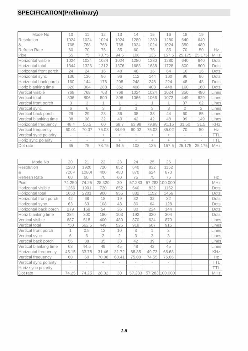
2.4.1 Maximum Resolution: Support to 1280 x 1024
2.4.2 Horizontal Size (Standard) 920±±±±8 mm (for mode 1〜〜〜〜26)Vertical Size (Standard) 518±±±±8 mm (for mode 1〜〜〜〜26)
More than 30FL(while pressing recall button to set default brightness)
b. raster background with contrast / brightness at Max. and black signal)less than 0.4FL
2.5. Operation:
Main unit button Main power switch (power ON /OFF)Power ON/OFFInput Mode (Video1 -> S-Video1 -> Video2 or S-Video2 ->Y/PB/PR 1 or Y/CB/CR 1 -> Y/PB/PR 1 or Y/CB/CR 1 -> RGB ->DVI->Video1 run in circle)Menu key -,+ Adjustment -,+
IR Remote Control Power on/offInput Mode (same as Main unit button)Volume -,+ Wide , Video/S videoinput:4:3/16:9/ZOOM1/ZOOM2Analog RGB input :W4:3/W16:9Menu -,+ Adjustment -,+ RECALLPIP ,POP ,SWAP ,MUTE
2.5.1 Adjustable Items:
AV/S-video input Brightness, Contrast, Color , Tint, SharpnessY/CB/CR Color Temperature
Analog RGB input
DVI input
Display position :Brightness, Contrast, Vertical position, Vertical width,Horizontal position, Horizontal width, Color TemperatureClock phase, DPMS.
AGC Figure Of Merit 50dB Min.RF signal range in which video at PDP drops 6 dB from output level obtainedwith 100mV input.
6.6 RF AGC Cut In Level 55dB ±±±± 2dB
6.7 FM/AM Rejection (100mV at SIF input) 14dB min
6.8 Noise Limits Sensitivity VHF 45dB max
UHF 49dB max
7. RELIABILITY REQUIREMENT: The MTBF needs 20000hrs under operation 25±±±±5℃℃℃℃(half luminosity, motion picture)
8. REGULATORY REQUIREMENTS:
8.1 Safety Requirement:
a. UL Safety of information technology equipment includingelectrical business equipment
b. CSA Safety of information technology equipment includingelectrical business equipment
c. TUV
8.2 Emission Requirement:The unit shall meet the EMI limits in all screen modes. For EMI testing, the unit must be failedwith the screen pattern consisting of scrolling capital “H” characters also the brightnesscontrast will be adjusted to max. Level.
a. FCC class A part 15
8.3 Transit test
SPECIFICATION VER1.0
2-7
a. Drop Test 200mm max.
b. Vibration Test
1. Forward and backward2. Right and left3. Up and down
Mode H-sync V-sync Video Power dissipationNormal Pulse Pulse Active Normal powerStand-by No pulse No pulse No video Power off
Pulse No pulsePower savingNo pulse Pulse
Blanked Less than 5 watts
This Plasma display is Energy star compliant when used with a computer equipped withDPMS.
Note: The power indicator LED color is green in normal state, yellow in stand-by
and power saving state.
9. VIDEO & AUDIO
9.1 Video Signal Output (impedance 75 ohm)
(input signal at 1.0 Vp-p ±±±± 0.2Vp-p)
1.0 Vp-p ±±±± 0.2Vp-p
SPECIFICATION VER1.0
2-8
APPENDIX A :
Preset Timing Chart
Item Description:A Total timeB Active display area including bordersC Active display area excluding bordersD Left/Top borderE Right/bottom borderF Blanking timeG Front porchH Sync-widthI Back porch