128
VLA Technical Report No. 36 MODIFICATIONS IN 1977 TO SOME OF THE L.O. MODULES D. S. Bagri March 1978
| Date post: | 26-May-2018 |
| Category: |
Documents |
| Upload: | vuongthuan |
| View: | 216 times |
| Download: | 0 times |

VLA Technical Report No. 36MODIFICATIONS IN 1977 TO SOME
OF THE L.O. MODULESD. S. Bagri March 1978


TABLE OF CONTENTS
1.0 INTRODUCTION.............................................. 1-12.0 LI: 5 to 50 MHz VCXO - REVISION B......................... 2-1
2.1 Modification Description and Reasons.................. 2-12.2 Drawings Effected.................................... 2-22.3 Drawings Enclosed.................................... 2-22.4 Input Output Connections.............................. 2-3
3.0 L6: 2 TO 4 GHz SYNTHESIZER - REVISION B................... 3-13.1 Modification Description and Reasons
Reference Block Diagram D13250B01..................... 3-13.2 Drawings Effected.................................... 3-33.3 Drawings Enclosed.................................... 3-33.4 Input Output Connections.............................. 3-5
4.0 L7: FRINGE GENERATOR - REVISION B......................... 4-14.1 Modification Description and Reasons.................. 4-14.2 Drawings Effected.................................... 4-24.3 Input Output Connections.............................. 4-3
5.0 L9:. CENTRAL LOCAL OSCILLATOR RECEIVER - REVISION C.........5-15.1 Modifications and Reasons............................. 5-15.2 Drawings Enclosed.................................... 5-15.3 Adjustment Procedure.................................. 5-25.4 Input Output Connections.............................. 5-45.5 Central L.O. Receiver (L9C) Module List of
Drawings, BOM's, etc.................................. 5-55.6 Bills of Materials for L9C............................ 5-75.7 L9 Module Photographs................................. 5-8
6.0 L10: CENTRAL LOCAL OSCILLATOR TRANSMITTER - REVISION C.....6-16.1 Modifications and Reasons............................. 6-16.2 Drawings Effected.................................... 6-26.3 Input Output Connections.............................. 6-36.4 Central L.O. Transmitter Rev. C (L10C) Module List
of Drawings, BOM's, etc............................... 6-46 . 5 B i l l s o f M a t e r i a l s f o r L 1 0 .................................... 6 - 6
i
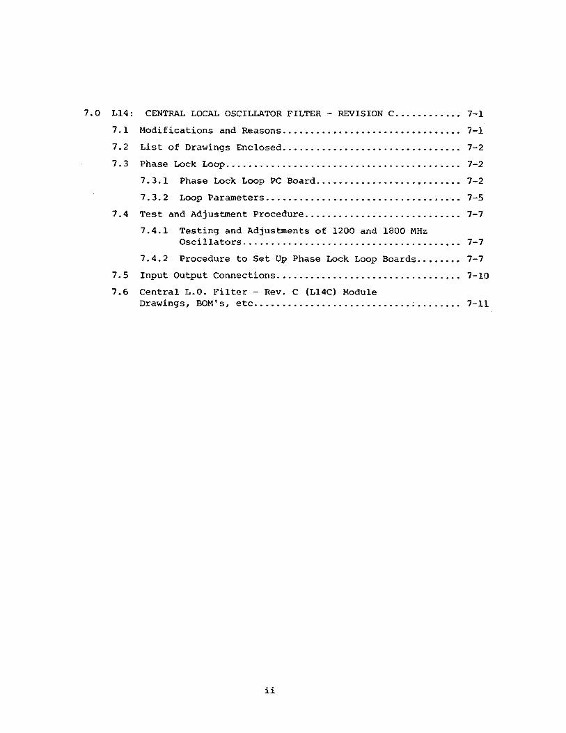
7.0 L14: CENTRAL LOCAL OSCILLATOR FILTER - REVISION C .......... .7-17.1 Modifications and Reasons...............................7-17.2 List of Drawings Enclosed...............................7-27.3 Phase Lock Loop....................................... .7-2
7.3.1 Phase Lock Loop PC Board .7-27.3.2 Loop Parameters................ . ...7-5
7.4 Test and Adjustment Procedure.......................... .7-77.4.1 Testing and Adjustments of 1200 and 1800 MHz
Oscillators .7-77.4.2 Procedure to Set Up Phase Lock Loop Boards .7-7
7.5 Input Output Connections................................7-107.6 Central L.O. Filter - Rev. C (L14C) Module
Drawings# BOM's, etc.......................... ........ .7-11
ii

LIST OF ILLUSTRATIONS
Figure 2.1 X10 Multiplier Schematic D13210S1
Figure 3.1 Block Diagram 2-4 GHz Synthesizer D13250B01Figure 3.2 Phase Lock Loop Board Schematic C13250S02Table 3.1 BOM: A13250Z10Table 3.2 BOM: A13250Z05Figure 3.3 Drive Circuit, etc. Schematic C13250S4
Figure 5.1 Block Diagram Central L.O. Receiver D13230B24Figure 5.2 5 MHz Receiver Schematic C13230S31Figure 5.3 Data Receiver Schematic B13230S32Figure 5.4 Level Indication Circuit Schematic B13230S30
Figure 6.1 Block Diagram Central L.O. Transmitter D13230B8Figure 6.2 5 MHz Modulation Driver Schematic B13230S2
Figure 7.1 Block Diagram Central L.O. Filter D13230B12Figure 7.2 Phase Lock Loop Schematic D13230S13Figure 7.3 Zero Crossing Detector Schematic B13230S26Table 7.1 BOM: Central L.O. Filter A13230Z33Table 7.2 BOM: Phase Lock Loop PC Board A13230Z32Figure '7.4 Damping Adjustment of Phase Lock Loop PC Board


1.0 INTRODUCTIONIn this report we describe the modifications made to some of the
Local Oscillator modules. A description of the modifications along with reasons for making the changes are given, and effected drawings are listed. Table 1 gives designations and names of the modified modules and their latest revision letter. Notes in Table 1 indicate the modules for which new Block Diagram (BD), Circuit Schematic (S) and Bills of Material (BOM) are included in this report.
TABLE 1: LIST OF MODULES MODIFIED
DesignationModule
NameRevisionLetter Notes
1. LI 5 to 50 MHz VCXO B S2. L6 2 to 4 GHz Synthesizer B BD, S, BOM3. L7 Fringe Generator B S4. L9 Central L.O. Receiver C BD, S, BOM5. L10 Central L.O. Transmitter C BD, S, BOM6. L14 Central L.O. Filter C BD, S. BOM
1-1


2.0. LI: 5 TO 50 MHz VCXO - REVISION B
2.1 Modification Description and Reasons
Description of Modification(a) Change resistors of ir attenuator
in 10 MHz output consisting of R26**, R27** and R28** from82 ft to 220 ft, 91 ft to 24 ft and 82 ft to 220 ft respectively.** means nominal Values of a 50 ft it attenuator, to be selected to give output power level to within ± 1 dB of + 17 dBm.
(b) Add a GPD 403 (Avantek) cascadable amplifier on X10 Multiplier PC Board between Til output and W1 coaxial cable whiph goes to 50 MHz output at L1J1. Provide + 28 V DC to the X10 Multiplier PC Board through a 0.1 pF RF1 filter feedthru (Spectrum control typeBE 001 DA 104 P) mounted on the multiplier enclosure. Connect the power to the GPD403 amplifier through a 62 ft, ht Watt resistor.
Reasons for Modification To increase 10 MHz output power at L1J2 from +10 to +17 dBm required for new scheme of distributing 10 MHz in B rack.
To increase 50 MHz output at LlJl from OdBm to + 10 dBm as required by phase detector in L2C.
2-1
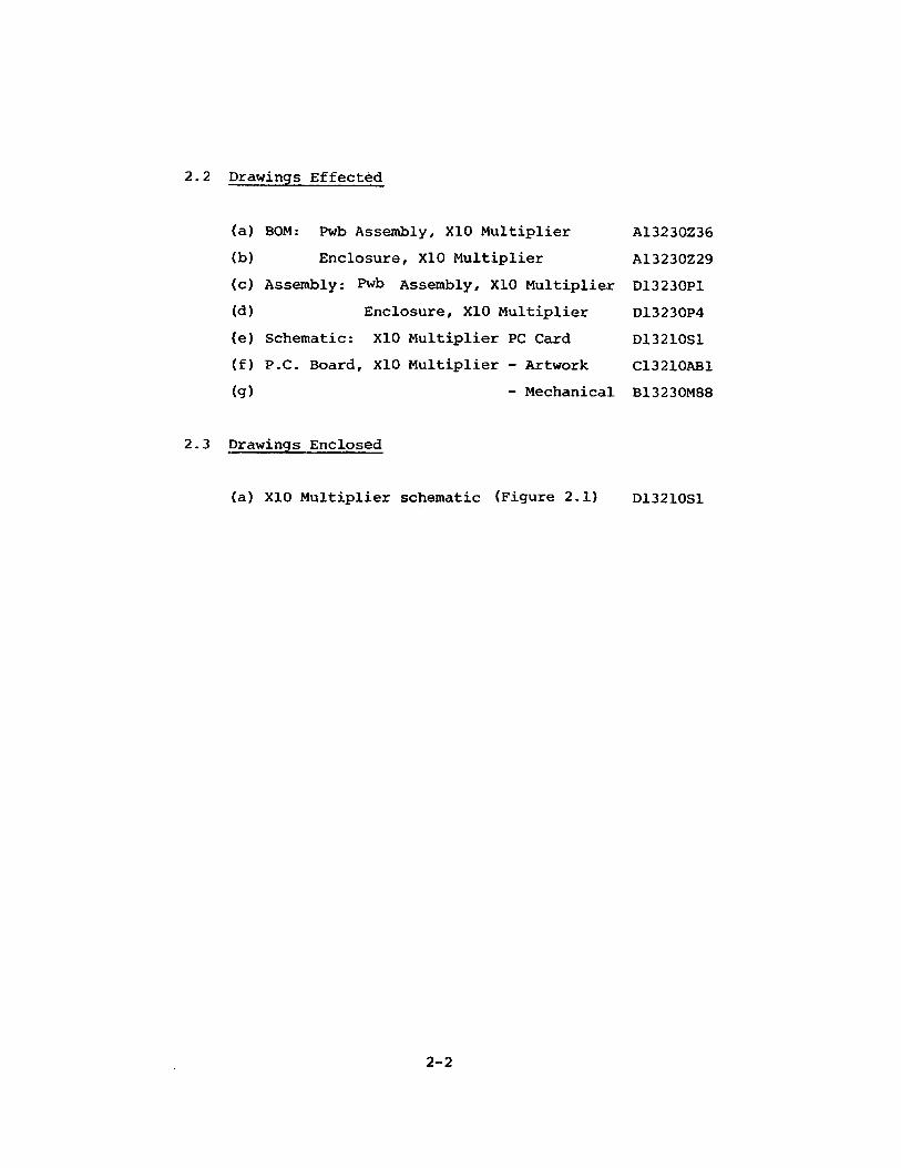
2.2 Drawings Effected
(a) BOM: Pwb Assembly, X10 Multiplier(b) Enclosure, X10 Multiplier(c) Assembly: Pwb Assembly, X10 Multiplier(d) Enclosure, X10 Multiplier(e) Schematic: X10 Multiplier PC Card(f) P.C. Board, X10 Multiplier - Artwork(g) - Mechanical
2.3 Drawings Enclosed
(a) X10 Multiplier schematic (Figure 2.1)
A13230Z36A13230Z29D13230P1D13230P4D13210S1C13210AB1B13230M88
D13210S1
2-2

8n v | o * r t | » u « » »
6 K J
w » y > •*
A 4 -f ~ - a m s + x i “ m
c MI P O S 0 A ' i P ' f J ' J " " « A o e A ¥ $ o \ c L a x
f i n ' .LfiMQlJ
B
KJOTE3:l,UKJLESS OTHERWISE SPECIFIED A. ALL RZ3/5T O R VALUES ARC IN
OHMS* I/4W a ALL CAPACITOR VALUES A X E
IKJ MICROFAfTAOQ e. * R 44 MAY O R MMUCrr BE USED
VALUC SELECTED O R ADJUSTED IN TEST 9. BRACKETED C O M P O N E N T3 /)RC L OCATED
OH OI3Z30PZ2 4.** NOMINAL VALUES, values selected to
GIVE OUTPUT LEVELS TO MAINTAIN± MB
w, our.(so m b *443 V±,K!
FIGURE 2.1.AST COMPONENT DESKS. USEO
R C (- u Q QR r± s SO 14 4 7 n
8
... C0MPOK1EMT CXSIG. MOT LKFDc c R
4g ?0NCxt A M Y JISUL
UNLESS OTHERWISE SPECIFIED DIMENSIONS ARC IN INCHUIWLCNMCUc MUI ft I lAMCNOMUUa* m I
7 I uL^LO 3Y3TCM
IHJCIMCMUU* *MATERIAL
II NISH:
XIO MULTIPLIER P. C. C/fRO
SCHEMATIC
NATIONAL RADIO ASTRONOMY
OBSERVATORYu~n>— awrsrwiMtr
hi ”wr
B


2.4 Input Output Connections
J7OJ9
O
J lloJ13oJ I5o
J8oJ10oJI2oJ I4oJ I6o
J lo J2
J3 oO J4oPI
_n_r _nJ
CONN FUNCTIONJl + 10 ± 1 dBm @ 50 MHz OutrmtJ2 + 17 i 1 dBm @ 10 MHz OutputJ3 + 10 * 1 dBm @ 5 MHz 6 OutputJ4 + in - 1 dBm (a 5 MHz Ont-put-.J7J 8 + 10 @ 20 MHz TerminatedJ 9JIOJ llJ I2J 13J 14J I5J I6
DOUBLE WIDE MODULE ( R E A R VIEW ) P! (REAR VIEW )
PIPI N | FUNCTION WIRE C O L O R PIN F U N C T I O N WIRE COLOR1 1 22 power 5 MHz 0 Red/Wht2 1 23 Power 10 MHz Ora/Wht3 I 24 Power 20 MHz Yel/Wht4 I 25 Power 10 MHz Drive Orq/Wht5 j 265 1 277 I 28 - 2 8 V D C * G R E E Ne l 29 + 2 8 VDC GREY9 1 . 30lO | -r 5 V D C * O R A N G E 31II | — 5 V D C * B R O W N 32\ z 3313 High Quality Ground 34 PWR. GR O U N D B L A C K14 3515 36IS + I5VDC RED 3717 — I5VDC * Y E L L O W 38 5 MHz-VCXO Cont. Volt. Co-Axial RG 174/U13 3919 | 4020 | 412 1 1 Power 5 MHz Brn/Wht 42 HIGH OUAL. GROUND ....
INDICATES A FUNCTION NOT FOUND IN THIS MODULE.
2-3


3.0 L6: 2 TO 4 GHz SYNTHESIZER - REVISION B
3.1 Modification Description and Reasons Reference Block Diagram D13250B01
Description of Modification(a) Change first mixer from MD525-4
(Anzac) to M1H (Watkins-Johnson).
(b) Change 2-way power divider PDM20-500 (Merrimac) at the output of 28 dB, 0.01 to 1 GHz amplifier to 10 dB directional coupler DCG-10-4 (Anzac). -10 dBc coupled port goes to L6J13 and the direct output to the phase lock loopPC Board.
(c) Add a 3 dB attenuator before 600 MHz LPF.
(d) Add a BPF 3B120-3000/500-0 (K and L Microwave, Inc.) between L6J9 and coaxial relay which selects between reference or alternate reference.
Reasons for Modification To get better isolation between L.O. and RF ports and operation from a high level mixer to a low level mixer.
To increase the output going to the L.O. port of the second mixer located on the phase lock board.
To minimize variation of signal levels between various 50 MHz harmonics (comb-lines) going to RF port of the second mixer located on the phase lock board.
To reduce leakage of YIG oscillator output from one L6 to another through 3000 MHz reference line.
3-1

(e) Replace 50 MHz comb generator by a 10 dB attenuator.
(f) Replace Cinch Barrier terminal block on which DC power supply connections are brought from AMP Connector by a filter mounting block (NRAO-B13440M31) and add0.1 yF RFI suppression filters (Spectrum control type BE001DA104P) in all power supply lines soon after AMP Connector
(g) Add resistors R36, R37, R38, and R39, C34 and C36 and diodes CR3 to CR6 on the PLL PC Board (see drawing "No. C13250S2).
Design changes of L2 and L3 modules provide phase stable 50 MHz comb; therefore, this comb generator is no longer required. A 10 dB pad is introduced to keep proper comb level to the phase lock board, which will minimize chances of false lock till a later day when the phase lock board is re-designed.
Filtering 100 kHz and 5 MHz floating around in the B rack. Also suppressing transients on power.supply lines, especially + 28 V when coaxial relays are switched ON and OFF in the L6.
RC time constants are put to reduce amplitude of transients and diodes are put to protect the CMOS analog switches from the transients.
3-2

(h) Add a series capacitor C35 and an inductor LI to ground at the L.O. port of the second mixer MD113 (Ul on the phase lock board - see circuit schematic C13250S2).LI = 0.1 yHC35 = 75 PF CHIP Capacitor
(i) Replace 1200 MHz low pass filter in the 50 MHz comb signal path by a 0.141” coaxial cable.
3.2 Drawings EffectedSee enclosed list - page 3.4
3.3 Drawings Enclosed
(a) L6 Block Diagram (Figure 3.1)
(b) Phase Lock Loop P.C. Board Schematic (Figure 3.2)
(c) Drive Circuit, etc.(Figure 3.3)
(d) BOM: L6 (Table 3.1)
(e) BOM: PLL PC Board (Table 3.2)
Filter out 10 MHz coming from0.01 to 1 GHz amplifier.The 10 MHz is generated due to finite isolation between two L6’s and intermodulation in the amplifier.
The design changes of L2C module requires that a 1050 MHz LPF is used inoutputs of the comb lines coming out of the L2C module. Thus, the 50 MHz comb spectrum is already limited to 1050 MHz and the 1200 LPF is no longer necessary.
D13250B01
C13250S02
C13250S4
A13250Z10
A13250Z05
3-3


fcWnmon
RAMQE3 W IT C I
rr
l .p ffc = <oOO MHz F L 2 ZG>
3dB ATTENUATOR*ww^-A Z 4 8
t:RANGESWITCH
\Oit>
BPF 3 0 0 0 /5 0 0 FL3 4 9
■I5t 3jBn,
3 0 0 0 M H *< J 9 REF.
&
<J8 50 MHz COMB-3 3 1 5 <g> EACH U H E
S E C O N D M IX E R ‘
-4<JBV\e 10 .\
10 tdBM<» D . I MWZ .F . REF.
'I. F."BMC-F.P
>-------
J)5> -
1
-4JBm<J!3 L O W F R E Q . O U T P U T
IO d B C O U P L E R
A l 4 *
240DMM*< J 7 A L T . REF.
F IR S T r M IX E R M l t G
10 MHz I.F AM P
X
PHASE LOCK U N IT A I3 2 5 0 Z 0 6
~ l- lOdBc
-IO dB C O U PLER
DC I 5
L O C K IN D IC A TO R
L
P H A S E D E T E C T O R
I
L O O PA M P
H IG H /L O W LO C K C O N T R O L
INTEGRATOR R ESET
C IR C U IT
±)O V COMPARATOR
± 7 .5 VCo m p a r a t o r !
f r o m data o— >- S E T
S E R IA L TO PARALLEL
CONVERTER]
TO DATA <- SET
TOD A T A -
S E T
PA R A LLE L T O SERIAL
CONVERTER
D R IVER FOR Y I G F M . C O IL * *
■*---<JI2 O U T P U T
3 4 * 0 -3 9 * 0 MWu/ # » [ /***■ * n * SO 4 10.1 M H t}
VIG-TUNJED OSCILLATOR Y l 5
DRIVER FOR Y IG TUNING! C O IL ■ * *
M A N U A L* T U N I N G
C O N TR O L
TO RELAYSfief./ALTERNATE [j H tC ,H /lO tV LOCK HIGH/10/y RANGtcov/urr* / manualCONTROL ✓SCAKC* IHNI&IT
M A N U A L\
+ IO VF IX E DR E F E R E N C E
C O M P U T E R
1D / A
CONVERTER
\Z B IT S
L A T C H
A D D E R
5 - B IT C O U N T E R
SE A R C HOs c il l a t o r
A N A LO GM U L T I
PLEXER
LOO P A M P V O LT A G E - « - © A /D O U T P U T V O L T A G E
P O W E R SUPPLY V O L T A G E S
PULSEINHIB ITSIGNALS
[ _ C O N T R O L C A R D A I 3 2 5 0 Z
NO TES:1. JT .Je .J^JIEJIB i JI5 ARE ON REAR
PANJEL.2. * = B.O.M. A I32.50Z08 , ITE M 15.
**= B .O .M . A I3 Z *5 0 Z 0 73.
EU-ITEM NO?S PER B.O.M. A I3 2 5 0 Z I0■REF. DESIGd. PER IEEE NO. 3)5 4 NR AO SPEC.
A. ALL POWER SUPPLIES IN MODULE ARE FIRST FILTERED U5INC* O .U F RFI FEED THRU5.
FIGURE 3.1
NEXT ASSY USED ON
UNLESS OTHERWISE SPEC IFIED DIMENSIONS ARE IN IN C H ESTOlCUUKt! MGLII ±>n.*c< occawu.sijtui' ±I M_»ee MC*UUJ : XX' ±lnjWMOHtll.il: ±
MATERIAL
L-G 2 -4 GHz
LSY_NTM£5!ZER BLOCK DIAGRAM
NATIONAL RADIO ASTRONOMY
OBSERVATORY*o»tfivut. V4. mci
E S B 1 I S S E EOATt3-lv-Tf
B
1


CZ7CXI
—vca 9
o-'ioHl® 7 a pr14 / vChTPJ2 1*4- 3 MHfV3/60 MH{ HARMONICA '45 2 54e»)/LIMr
’ w «X ‘-° :
> R© I R5><20K ;iso T
- 10
MONrroc(0.1 MHt
UOCKCCWR. “ TZ-oJ ( UOfcJC MK5H» l l y j
V41QH lflCK> — 5 J4*tO*WBw Mr*N 10.1 IMt
C M -IH914
VJOTW:1. UKlLtrSft orrwW'Wlt WrCINkO.’ a . Au. R*-»tyrop.v A «t tv) Oum^ , tx AU. CAPAC1TOC* AAir WJ .
t A** M r4tON«nc*}« UMrO,*Of*£3jCyrw»J C3& CM THRU C Q & ,J\ 'TUbJ X*. FU ,
a i Q t , iu tmou M 9 . u i Tw«a o a , U .6. W«m«rMC» 0*«d|MKnOM« Nfinr UM<7;
C44. POR ©OM. 5£E A 13230 CO^
D PJ0 /1001 JS ifrft At it, /J«A
c %AODeo:u, Q3H nw **9C3d. T//I.UJC3C- mo cea T//uu <
a#?i?4.v■}.:■*- e.jriiv/.9K (?i-c'S6. dTcorv nrtu ioco PJO. t?iS' 510*2 n»S e.4K c?d, <ow nss s
A ^hfoeveesep Wx'TfWCHu* na< z<9«as n < R23<?4 im t .*<fttv 04f| VI t r m i ' e H Pi t . * e t. m
f r o * a n i *YtJTw*51!**lG»
PHMIr LOCK * 6- &044P e«w«rM nc PMAVW
NATIONAL RADIC ASTRONOMY
OBSERVATORY

FIGURE
u>Iu

List of L6 Drawings Effected
I. 2-4 GHz Synthesizer Module (L6) Drawings, Artwork & Bills of Materials
Schematic & Logic Diagrams Phase Lock Unit C13250S2
.... -&i~3~2503"3'Drive Circuits Etc. C13250S4Control and Interface Card D13250L3Bills of MaterialPhase Lock Unit A13250Z5Phase Lock Unit Enclosure A13250Z6Driver Board A13250Z7Front Panel Assembly50 MHg Harmonic Gen..------ ------------------ A13250Z8
-- --------------- A-1325Qg»Component PlateControl and Interface Card
Assembly Drawings2-4 GHz Synthesizer Phase Lock Unit P.C. Board Phase Lock Unit Enclosure 50 MHz Harmonic Gen.Front PanelControl and Interface Card Driver Board
Wiring ListsControl and Interface Card
Printed Circuit Board
Phase Lock Unit■50 Mila Harmonic Generator-
ArtworkC13250AB6 <- -A-132-50AD7—
Silk Screen - C13250AB5 <-
Driver Board Meter Resistor Board
Mechanical Drawings
B13250AB3B13250AB8
B13250AB4
Rear Panel Front PanelBar Supports, Right Side Bar Supports, Left Side Top & Bottom Cover Side Plate Component PlateMixer and Coupler Mounting BracketFilter Mounting BracketsMounting Brackets for 100-pin Connector GuideTuning CoilPhase Lock Unit Enclosure Wire Wrap Board
Effected
Effected
Effected
A13250Z10 <- A13250Z11
D13250P7C13250P5C13250P6
Effected
EffectedEffected
C13250P8 Deleted C13250P9 C13250P10 B13250P11
A13250W3
Drill Drawings D13250M20 «- .EffectedC13250M24 DeletedC13250M23B13250M25
B13250M11C13250M12B13250M28 (Parts 1&2) B13050M28 (Parts 3&4) C13050M22-2 B13050M18C13250M21 --- EffectedB13250M27 ----EffectedC13250M26B13250M15B13050M4C13250M29C13250M22D13520M1
3-4

3.4 Input-Output Connections
OMQConnector
J7J8J9J10JllJ12J13J14J15J16
PI (REAR V IE W )
-15 ± 2 dBm @ 2400 MHz 50 MHz Comb -33 ± 5 dBm/line -15 ± 3 dBm @ 3000 MHz
+16.5 ± 1.5 dBm @ 3.49 to 3.99 GHz First IF OUT
+10 ± 1 dBm @10.1 MHz
InputInputInput
Output
Input
3-5

Pin Function Pin Function
A +15 V P Enable Signal, Sub MuxB Ground Add. 10 (Low True)C +5 V r Enable Signal, Sub MuxD Add. 11 (Low True)E -15 V s Enable Signal, Sub MuxF Add. 12 (Low True)H Analog MUX. Input Ch. 3 t Enable Signal, Sub MuxJ Add. 13 (Low True)K u Enable Signal, Sub MuxL Ground Add. 14 (Low True)M Address Bit 1 (LSB) V Enable Signal, Sub Mux
(Low True) Add. 15 (Low True)N Address Bit 2 (LSB) w Analog MUX OUTPUT (High)
(Low True) X Analog MUX OUTPUT (GRD)P Address Bit 3 (LSB) y
(Low True) z Analog MUX INPUT Ch. 7 (+28V)R Address Bit 4 (MSB) AA
(Low True) BB GRD. Signal, GRD. DigitalS Serial Input (Low True) CC GRD. Signal, GRD. DigitalT Input Lock (Low Ture) DD GRD. Signal, GRD. DigitalU Input Strobe (Low True) EEV Serial Output (Low True) FFW Output Clock (Low True) HHX Output Strobe (Low True)Y Input Enable In (Low True)Z Output 1 Enable (In)
(Low True) a Output 2 Enable (In)
(Low Ture)b Enable Signal, Sub Mux
Add. 0 (Low True)c Enable Signal, Sub Mux
Add. 1 (Low True)d Enable Signal, Sub Mux
Add. 2 (Low True)e Enable Signal, Sub Mux
Add. 3 (Low True)f Enable Signal, Sub Mux
Add. 4 (Low True)h Enable Signal, Sub Mux
Add. 5 (Low True)j Enable Signal, Sub Mux
Add. 6 (Low True)k Enable Signal, Sub Mux
Add. 7 (Low True)m Enable Signal, Sub Mux
Add. 8 (Low True)n Enable Signal, Sub Mux
Add. 9 (Low True)
3-6

TABLE 3.1:
BOM: A13250Z10
DILL OF MATERIAL NATIONAL RADIO ASTRONOMY OBSERVATORY
[T1 ELECTRICAL QT] MECHANICAL BOM # A13250 ZIP REV A DATE __________ PAGE 1 OF __ 3
MODULE # L6 NAME 2-4 GHz Synthesizer DWG # D13250P7 SUB ASMB Component- Plat-*_______ DWG # _______
SCHEMATIC DWG # ___________ LOCATION ___________ QUA/SYSTEM _____ PREPARED BY c- pace APPROVED ________
ITEM#
REFDESIG
MANUFACTURER MFG PART # DESCRIPTION TOTALQUA
1 NRAO A13250Z10 Component Plate Assembly —
2 NRAO C13250M21 Component Plate 1
3
4 Merrrmac Anzac fiSSLi&sbo-10 dB Directional Coupler Power-Sprtrtrter 1
5 Omni Spectra 20054-3 0 Directional Coupler 1
6 Aneae- Watkins-Johnson M1H Mixer 1
7 NRAO B13250M27 Mixer-Coupler Mounting Bracket 1
8 NRAO C13250M26 Filter Mounting Bracket 1
9 H. H. Smith 8370 Spacer <1-3/4" long x 8-32) 6
10 #8-32 x 5/8 LG Socket Head Screw 6
11 #4-40 x 1/2 LG Flat Head Screw 2
12 #4-40 x 1/2 LG Pan Head Screw 4
13 #4-40 x 1/4 LG Pan Head Screw 11
14 #6-32 x 3/8 LG Pan Head Screw 4
15 #2-56 x 1/4 LG Socket Head Screw 14
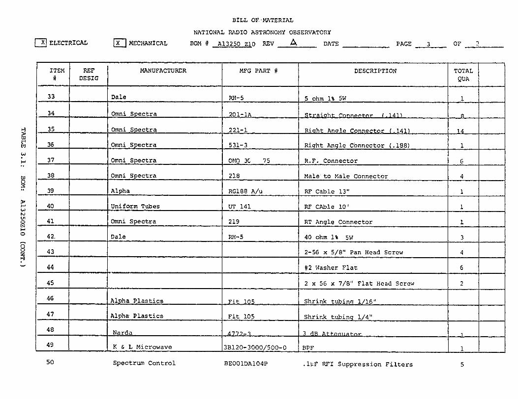
TABLE 3.1:
BOM: A13250Z10
(CONT.)
P H ELECTRICAL
BILL OP.-MATERIALNATIONAL RADIO ASTRONOMY OBSERVATORY
[F I MECHANICAL BOM # A13250 ZIP REV A DATE PAGE 3 OF

TABLE 3.2:
BOM; A13250Z05
BILL OF MATERIAL NATIONAL RADIO ASTRONOMY OBSERVATORY
| x 1 ELECTRICAL \ ' ] MECHANICAL BOM # An?c;075 KEV -B- E DATE PAGE 1 _ _ OF ^
MODULE it L6 NAME PHASE IPf.K 1IMTT FMHl njsllHF DWG # C13250P6 SUB ASMB P.C. ,B0ARD__ASS_1Y________ DWG # CJ.3.25.QP-5.SCHEMATIC DWG if ___ _______ LOCATION ____________ QUA/SYSTEM ______ PREPARED BY Cv Pace APPROVED _________
ITEM#
REPDESIG
MANUFACTURER MFG PART # DESCRIPTION TOTALQUA
1 N..R.A.0. A13250Z5 PC BOARD ASS1Y
2 N.R.A.O. C13250M20 P.C. BOARD 1
3 Robinson Nuggent 1CN163-S3 16 Pin Socket ‘(Dip) 2
4 Robinson Nuggent DP5178 8 Pin Socket (Round) Z
5 Birtcher 3AL 635 2R Heatsink 1
6 Robinson Nuggent 1CH083-S3 8 Pin Socket (Dip) ......L
7 Robinson Nuggent 1CN143-S3 .14 Pin Socket (Dip) 2
8 Cinch 3LPS-B Transistor Socket 2
9 Keystone 1502-3 Terminal ....i o Thermalloy
2266B Heatsink l
ii Robinson Nugent MP12100 12,Pin Socket l
12 A Anzac MD113 Mixer i
13 • FL1-2 K fi L 4B51-10/5.5P___ Filter. ------ 2
14 U7 RCA CA 3076 RF Limiter 1
15 Q 1-2 RCA 2N 5179 Transistor 2

TABLE 3.2:
BOM: A13250Z05
(CONT.)
BILL OF MATERIALNATIONAL RADIO ASTRONOMY OBSERVATORY
P H ELECTRICAL Q ] MECHANICAL BOM it A13250Z5 REV E DATE ___________ PAGE 2 OF ___4.
ITEMft
REPDESIG
MANUFACTURER MFC PART # DESCRIPTION TOTALQUA
16 U4 Motorola MC12040 Phase Detector 117 U8 National LH0032C RF Amp 118 U5 Raytheon RC4558DN Op Amp 119 U2 Siliconix DG190BP Fet Switch SPDT 220 U3 T. I. 74S00 Nand Gate 121 . CR1-2 IN914 Diode 222 Rll, R12 Resistor 51 ft, 1/4 W, 5% 223 R6 Resistor 150ft, 1/4 W, 5% 124 RIO, R15
R31, R17 Resistor 2.2K ft, 1/4 W, 5% 425 R8 Resistor 20K ft, 1/4 W, 5% l26 R7 Resistor 3.3K ft, 1/4 W, 5% 127 R9,R3,R1- 100 ft 328
R5, R 19 R16 750 ft 3
29 R4 30 ft " T30 R2, R22
R25 » 470 ft 331 Rl 47 ft " 132 R20, R26 " 130 ft " 2

TABLE 3.2:
BOM: A13250Z05
(CONT.)
NATIONAL RADIO ASTRONOMY OBSERVATORYr— , 'J) y jy Hr] ELECTRICAL [^] MECHANICAL DOM If A1325QZ5 rev __________ DATE £ .0# PAGE 3 OF
ITEM#
REFDESIG
MANUFACTURER MFG PART # DESCRIPTION TOTALQUA
33 R21,R27 Resistor 390 U, 1/4 W, 51 234 R32,R30 " 510 Q " «* 2
35 R28 /R29 2.4K ft 236 R33 IK ft 137 R18,R14 120 ft 238 R34,R35 Helitrim 63WR " 10K Pot 239 C17 Erie 814-050-651103M Red Cap .01 uf Capacitor 140 * Erie 8121-050-651 104M Red Cap .1 uf Capacitor 12
41 *★ Erie 8131-050-651 105M Red Cap 1.0 uf Capacitor 742 C23,CS6 ERIE MONOBLOCK CK05BX472K 4700 pf Capacitor 243 C19,C18 Arco DM 15101J 100 pf Capacitor 244 C24 Arco DM 15100J 10 pf Capacitor 145 U6 Siliconix DG200 Fet Switch *SPDT 1
46 ALPHA22 AWG 8021-100 TINNED COPPER
WIRE, BUS 6in.
47 PENNTUBE PLASTICS CORP.0-6591A, 22AWG
1W, NATURAL TEFLON TUBING 6 in.
48 R23, R24 Resistor, C,7K, 2
49* C15', C14^ C 1 2 t C13^ Cl', C27 CIO*, C7^ C57 C6T Cll‘7 C8"** C3, C9 CZOf C2lT C23-, C22T C16

TABLE 3.2:
BOM: A13250Z05
(CONT.)
BILL OF MATERIALNATION T*L RADIO ASTRONOMY OBSERVATORY
f~ 1 ELECTRICAL [ X | MECHANICAL BOM A13250Z5 REV _________ DATE PAGE
ITEMIf
REFDESIG
MANUFACTURER MFG PART # DESCRIPTION TOTALQUA
50 Waldon NW 875 Flat Washer No. 4 Nylon 4
51 4-40 X .250 LG Screw, Pan Head, S.S. 4
1R f i j i j l o r l k , ' k . w • V
C34/ C36• 0 1 A v p z .
f t
------- )------------------
C35h t C f o d B Q V i V ' )
l o o g - l s o - J - p - s n I S p r c k \ } > G u p u c i j e y I
5 ? U0*1 1


4.0 L7: FRINGE GENERATOR - REVISION B
4.1 Modification Description and Reasons
Description of Modification Reasons for Modificationa) Replace IC at position 8D on WW
board (from type 74196) by Texas Instrument type 74S196 (Schottky TTL) or equivalent. This is a pin compatible replacement.
(b) Add filtering components in the DC power supply lines just before they leave the module as shown below:
Cl*To X' TAL FILTER <--- ''TTZRP1-- = ---<
U N IT 22 pH f T l
Existing IC had marginal switching speed, unsatisfactory to guarantee reliable performance. Therefore, replaced by a faster switching speed device.
To filter out 100 kHz and other switching signals leaving out on power supply lines from the module.
+ 15 V DC FROM Pl-16
Cl 0.0 mH, .1 Q
T [
J,To WW CARD I -J_ - - < +5 v DC
r f - j FROM Pl-102.2 yF
Cl’To WW CARD < ------------<
2.2 yF -
- 5 V DC FROM PI-11
* ExistingCl: 0.1 jiF RF1 Feed thru' (Spectrum control type BE001DA104P)
4-1
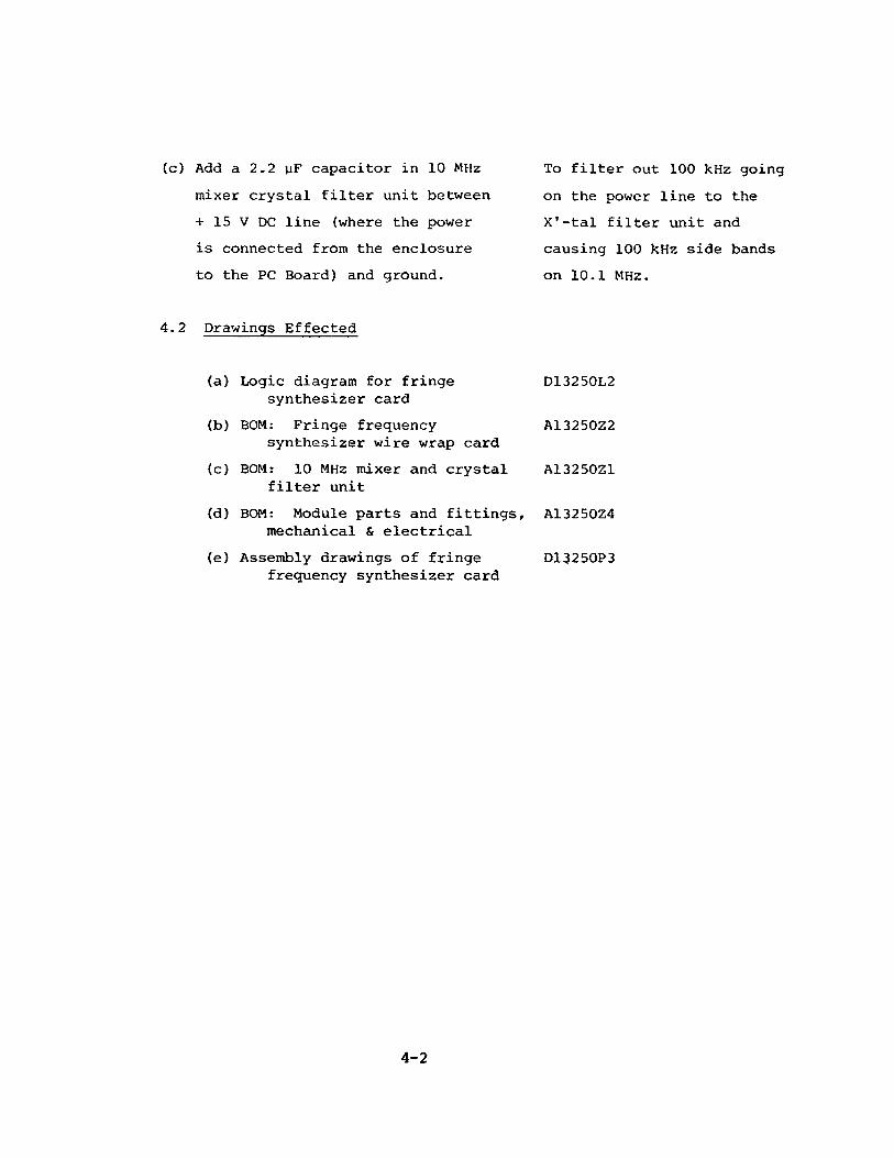
(c) Add a 2-2 uF capacitor in 10 MHz mixer crystal filter unit between + 15 V DC line (where the power is connected from the enclosure to the PC Board) and ground.
4.2 Drawings Effected
(a) Logic diagram for fringesynthesizer card
(b) BOM: Fringe frequencysynthesizer wire wrap card
(c) BOM: 10 MHz mixer and crystalfilter unit
(d) BOM: Module parts and fittings,mechanical & electrical
(e) Assembly drawings of fringefrequency synthesizer card
To filter out 100 kHz going on the power line to the X'-tal filter unit and causing 100 kHz side bands on 10.1 MHz.
D13250L2
A13250Z2
A13250Z1
A13250Z4
D13250P3
4-2

4.3 Input-Output Connections
CONN FUNCTION 1J l -He>±HSr*@ MrtHz 1J2 + 1~± 50MHz. 7*. bu£ 9J3 —|C>±. 1 {oKHz ~ 1J4 i
-nJSINGLE WIDE MODULE
( REAR V IE W )
+ O
® 8) _ (l 0) (3) ©
@ (i?21
© @ ©
©2©& Z Q
© ©© @
© @ ©GND
+ o
PI (REAR V IE W )PI
PIN FUNCTION WIRE COLOR PIN FU N C T IO N WIRE COLORPhase Switch Control Ir 22 Inable Sub__MPT.Y A.HH n19.2Hz Clock Pulse In 23Output Strobe 24Input Clock 25100 kHz Ref.. Tn 2 6
272 8 r-2&-VO-C Signal GRP
8 Output Clock 29 *f-2B-V£H2- Signal GRD GR-E-Y
inpH.fr.. S.tr.Pke 30 Snable Sub. MPLX Add. 610 + 5VDC ORANGE 31 f t t i
II — 5V-D-6 -5.2 VDC BROWN 32 lonitor Word Bit 2212 Serial Input 33 Signal GRD13 Serial Output 34 PWR. GROUND BLACK14 Address Bit MSB 35 Monitor Word Bit 2315 Address Bit 3 6 Monitor Word Bit 2416 + 15 VDC RED 3717 - I 5 V D C YELLOW 3818 Address Bit 3919 Address Bit (LSB) 4 020 Input Enable (Rate) 41
Input Enable (Phase) 42 HIGH QUAL. GROUND* IN D IC A T E S A F U N C T IO N N O T F O U N O IN T H IS M O D U L E .
4-3

5.0 L9: CENTRAL LOCAL OSCILLATOR RECEIVER - REVISION C
5.1 Modifications and Reasons - Reference Block Diagram D13230B24This module has been extensively modified. Main reasons
for the modifications are following: Input signal levels at 1200 and 1800 MHz may be grossly different. Therefore, to provide specified levels at 1200 and 1800 MHz, to 5 MHz Receiver and Data Receiver respectively and also at Output from the module, it is necessary that gain at each frequency can be varied independently. Also, external detectors at 1200 and 1800 MHz to provide signal at 5 MHz and Data respectively have been replaced by built-in detectors inside 5 MHz Receiver and Data Receiver boxes. For incorporating detector circuits and to provide front panel monitoring of 1200 and 1800 MHz levels going to the two receivers, the circuits of 5 MHz Receive and Data Receiver have been modified.Also, output of the 5 MHz Receiver has been modified to make it compatible with digital phase monitoring using f = 19.2 Hz off-set. Circuit for monitoring level and adjusting gain at 1200 and 1800 MHz have been added.
It has been noticed by Larry D*Addario that presence of IF signals, along with 1200 and 1800 MHz L.O. signals at the input of the L9 module (L9J1), causes compression in the first 19 dB gain amplifier AR1. Modification to correct this problem is under investigation.
5.2 Drawings EnclosedMost of the drawings connected with L9A have been effected.
A list of new drawings is enclosed. Following drawings are enclosed in this report:
(a) Block Diagram - Central L.O. Receiver (Fig. 5.1) D13230B24(b) Schematic - 5 MHz Receiver (Fig. 5.2) C13230S31(c) Schematic Data Receiver (Fig. 5.3) B13230S32(d) Schematic Level Indication Circuitry (Fig. 5.4) B13230S30
5-1


’DATA" ONC FRONT PANEL
NOTES'./. PI-PO W ER CONNECTOR Z.
ATI ■f - ITEM NUMBERS PER SOM A /3Z90E 07 ■ REV DESIG. PER /££ £ NO. S/S 4 NfHO SPEC.
FIGURE 5.1
NEXT ASSYA tttS O Z O l
USED ON
UNLESS OTHER W ISE SPECIFIED DIMENSIONS ARE IN IN C H ESr a U M U C tl: AM Ottl ±IFL A C t M C M A L tl .u n : ±I n j> c t tXCrnALt I.VO; *
I n_ACl C*C*»|J(.X): ±M ATERIAL:
FIN ISH:
'79* CENTRAL L.O.
l — 8LQ£/y££L-.i SLOCK D/AGRAM
TSffrrJm u .
NATIONAL RADIO ASTRONOMY
OBSERVATORYC*U*lOTUtVH.L*. YA. m et
'Wa***y" ~ l&Atl
S•2SD/3Z30K41SCft”>-<*- ft


5.3 Adjustment Procedure
5.3.1 5 MHz RECEIVER - Reference Schematic C13230S31 (Fig. 5.2)
(a) Apply a total of - 4.5 dBm power at 1200 MHz with normal 5 MHz sidebands on it (- 10 dBc at ± 5 MHz from carrier at 1200 MHz) to the receiver input from a 50 fl source (DC return is required).
(b) Set R22 on U2 to provide about 0.5 V at output of CR1 (Pl-21).
(c) Apply a + 8.5 ± 1.5 dBm signal at 5 MHz + f (wheresf =19.2 Hz) from the master local osciallator system sto L9J9. Adjust DC offset pot R17 to give symmetric cal 19.2 Hz (symmetrical around 0 DC) as measured at *5<|>f monitor front panel BNC jack.
5.3.2 Data Receiver - Reference Schematic B13230S32 (Fig. 5.3)
(a) Apply a - 4.5 dBm power at 1200 MHz with normal± 5 MHz - 10 dBc sidebands from a 50 DC return source to the input of Data Receiver.
(b) Tune capacitor Cl in 5 MHz trap to observe minimum 5 MHz at Data Receiver output. It should be less than 50 mV pp.
(c) Apply a - 4.5 dBm power at 1800 MHz with normal ± 500 kHz - 15 dBc sidebands from a 50 DC return source to the input of the receiver. Check that output at Data Monitor BNC jack on front panel is 100 mV peak.
5-2

ii3
dpwmp npa nnpii'WIHP T V
C/7 .00In f
^ f * r i sro avc i mwc. ~ ' ** CKT,
CRZ—\ S052-&24
r ssrsratV 4hMOWUO CM I 5 4 M O k it TOG
MoNTMMn\ j6 •I___ X_____ I
! F
R33AAi A~*“^CR3±tN 47 33
j - H ( -re?” | .001 |i
j MONITOR |
KJOTEStt. U U U 3 3 OTHEZWt SE 5P£C/r/£D :
A. ALL Z E 3 I3 T O * VALUE3 A(?£ i k l OH M 3 y f /4 W
O. ACL C A P # C /T O * V /tLU E 3 APE fKi MtCeOFA!?AC>3
Z. 8*ACK£TED COMPOKIEKit s A f?S LOCATED OKJ 0 /3 Z 3 O P 2 3
3. P?£S€T eez TO t.tkr4. FOR &.0M. s$££ A/3230E7Z
LAST COMPOUeUT Off?Vd U3£DR C CR U Q L J54 3 3 t / 6
J
UNLESS OTHERWISE SPtClflEO OIMENSIONS ARC IN INCHEStpuuiKn Mkii a ;IruKt MCaMLll.HUI: a I K M I H C W U I U k * l * U a M C W U I . < l : *
MATERIAL.
FINISH:
I
L9LO.J?EC£/V£&
NATIONAL RADIO ASTRONOMY
OBSERVATORYV4 >*UWWi- - ' "' ‘MU" mM te d L .
im & s -•y*. t *»'<3-75

FIGURE
!f i » r f e v K B 5 M H i r P A PI m F I ' >■> / f r a INiJtC. tK ¥, ----= - f vAAAA-
t f lI
U )J - / ;
,f S F fC >C! E D :■ 'ILU£'~ / ) ? £
/ ; v \
\ W UEU /*(?£f t ; > ' - . - . ^ s
... •
■ : ■ ~ ' J-Z'5 j r '-.'S*VMTfOKJ
•. o - . ' j . - i f r . ' i i f s j e t o z D . 4. A?/? AQM 5££ AI3Z3027Q
H JCWfTiCW
M O U N T E D o nff(OHT PAbiet
c = ) - r i - z z
r LAST CQMPoUEbJT_p E S /$JJSED_C Z '
2
iC -J L > 6/13 / /2 2
N m ASSY tJSI 0 ON
U N I I S j O T H I R W I S I S P L C I F l t D D I M ! N l. i O N S A R t I N I N C H E S1(" • ■ •>’. ' . AN*.i I ■, .•I n v i • i Mil <, M i '
» i K I i 1 • -X l \ «l r ! l\ >■■ i ; . . viA' s .«• •»
M A I I MA !
I INIMI
£.7 CE>.!7FS\L C :~' _ _ _ \ l £ u f - '
/v r-'/i/f/cS C h r / . i ' . / / - :
' J i l
NA1K MAL RADIO .-S '■ I'ONOMY
1 I? VA (OKY
/ - 5 ; 7^
<J-/6-75’ ■' r ijrt '>h

5.3.3 Level Monitor Circuit - Reference Block Diagram D13230B24
(Fig. 5.1), Schematic B13230S30 (Fig. 5.4).
(a) Connect nominal (- 4.5 dBm) input signal at the
input of 5 MHz Receiver (Data Receiver) with normal
modulation on 1200 (1800) MHz carrier.
(b) Adjust potentiometer R1 (R2) on Level Monitor Board
with the meter switch connected towards 1200 (1800) MHz
side so that the meter reads zero.
(c) Check by varying the input signal to 5 MHz Receiver
(Data Receiver) by + 1 dB that the meter reads ~ + 5 p A
for the meter switch connected to 1200 (1800) MHz side.
(d) Remove the signal to 5 MHz Receiver (Data Receiver)
and normalize connections.
5.3.4 1800 and 1200 MHz Amplifier Gains in the System Reference Block Diagram D13230B24
(a) Connect the module in a normal system.
(b) With the module front panel switch on 1800 (1200)
MHz side adjust the front panel potentiometer Pot-1
(Pot-2) to give zero meter reading.
5-3

FIGURE
5-4
•H5V O- E4
El-O-
CaKiDO—E3
■VWVAA— R3 2 .2 K
1600 METER „ , ADJUST
CR2
* CRI --IM9I4
I
1200 METER ADJ. «•--■■ O E2
R2IK
R4.2.2 K
O E 5-I5V
METER BOARD-BI3230PGI
F - f ^ l 4 - 4
L2.
------------ ( f r o m o a t a r e c e iv e r
(MOUNT B O o ti FRONT P N L)
—< F R O M 5 MM? R E C E IV E RSWITCHZ pole - 5 POS.-CENTER OPT SPRING LOADED JBT TYPE 227
(M O U N T E D ON FRONT P N L )
M ETER 50-0-50
(MOUNTBO ON FR O N T PNL )
liNl i ' M Mf r(;,r,| <,(•(( if || [•(•.Vi f. v')NS Af<fr IN INCH( r> '■ •'■*.■. i , •
? ' /. ■ • VAIS '« •_------------- ---------------_ MA ! | 1- • 1
----------A/3230E77 : If.' ! 1
»t /\* sY 1 I «•.*( ---. . .. i.... . ........ ....... i.
A!L E V E L INDICATIONCK T
SCHEMATIC, D IA G R A M
r;\i ■ mai. radi o••'■ (ONON'Y
RVA1 ( ■i-:v
.(UTcS.
1-4-76
fe-477(• >0-?i >
1- B I3230S30

5.4 Input Output Connections
----L_n
J7 Jlo J8 o J2
J9 o J3 oo JIO o J4
Jl! o oPI
oJ I5o
J I4oJ16o
T TJ
CONN FUNCTIONJl 1.2&1.8 GHz -13 (-10) [ - 4 ] Input
J2J3J4J7J 8J 9 +8.5 ±1.5 @ 5 MHz + fe * Input
JIOJllJ12J 13 0 ± 0.5 dBm @ 1200 MHz. Output
J 14 0 ± 0.5 dBm @ 1800 MHz OutputJ 15J 16
LEGEND: All power levels in dBmNo paranthesis - each L.O. carrier, paranthesis - total L.O. powert
DOUBLE WIDE MODULE bracket - total IF & L.O. power,f = 19.2 Hz.
+
© © © fee) CO)© © ©
© ©© © ©
© ® ©
©@©@ ® o© S ©
© ©
© ~ © ©
© ©
GND
( R E A R VIEW ) . P I (REAR VIEWn r » t - r n n n o f ' t f l ^ i n a f p r f t c a n f _______________
Pi
P! N | F U N C T I O N WIRE C O L O R PIN F U N C T I O N W I R E C O L O #
1 1 22 Received data level
2 1 23
3 I 24
4 | 25
5 | Data out (TTL) Co-axial 26
6 27
7 5 MHz Phase-error 28 - 2 8 V D C * G R E E N
8 i 29 + 2 8 V D C * G R E Y
9 1 30
10 | -4- 5 VD C O R A N G E 31
II I - 5 V D C * BROY/N 32
12 | 33
1 Hiah aualitv around 34 PVVR. G R O U N D B L A C K
14 | 35
15 | 3S
IS | - M 5 V D C RED 37
17 | — 15VDC Y E L L O W 38
13 1 3913 | 40
20 | 41
21 I Received 5 MHz level 42 HIGH QUAL. GROUND
INDICATES A FUNCTION NOT FOUND IN THIS MODULE.
L9 5-4

5.5 Central L.O. Receiver (L9C) Module List of Drawings, BOM's etc.
Block Diagram
Data Receiver Schematic
5 MHz Receiver Schematic
Level Indication Circuit Schematic
Bills of Materials
Central L.O. Receiver
Data Receiver
Data Receiver PC Board
5 MHz Receiver
5 MHz Receiver PC Board
Level Indication Circuit
Assembly Drawings
Data Receiver PC Board
Data Receiver Enclosure
5 MHz Receiver PC Board
5 MHz Receiver Enclosure
Level Indication Circuit PC Board
D13230B24
B13230S03, S32
C13230S04, S31
B13230S30
A13230Z07
A13230Z16, Z17
A13230Z78
A13230Z18, Z19
A13230Z76
A13230Z77
B13230P66
B13230P28
B13230P65
B13230P23
B13230P61
Printed Circuit Boards, etc. Art Work
SilkScreen Mechanical
Front Panel
Data Receiver PC Board B13230AB09
5 MHz Receiver PC Board B13230AB04
Level Indication Circuit Board
B13230AB33
B13230AA24 B13230M33
B13231M15
C13230M55
B13231M19
Wire List (Module) A13230W07
5-5

Mechanical
Central L.O. Receiver
Partition Plate
Guide
Cover, Perforated
Right and Left Side Plates
Panel, Rear
Bar Support Top and Bottom-Left
Bar Support Top and Bottom
Data Receiver/5 MHz Receiver End Plate
" " /Side Panel
5 MHz Receiver
Turret Terminal
D13230M61
B13230M04
C13050M22-1
B13050M18
C13210M04
B13230M36
B13050M23
B13230M89, M90
B13230M29, M30
B13230M27
B13230M39
B13230M54
B13230M98
5-6

5.6 Bills of Materials for L9C
5-7


V I A D A T A L I S T I N G
M^PULE: L09 PROJECT NO• 13240 DRAWING NO. J A13230707n&TA S F T : CFNTPAL 10 PPCPIVPR POM I CENTRAL 1.0 PFCF IVER
MDO-O/S-Q/M OESCP VALUE MFC,. PART NO. MANUFACTURER ITFM# BOM# DESCRIPTION
109 NST A1323QZ0? NRAO 1 A13230Z07 CENTRAL LC RECE IVER 0LOO 1 MPM D13230M61 NfcAO 2 A 13 2 3 OZ 07 PAP Tl Tl ON P L i T P M109 4 MPM RI3Q50M04 NP AO 3 A13230Z07 GUIDE Z109 2 MPM C13050M22-1 NRAD 4 A13230Z07 COVER,PERFCPATEC K109 2 MPM B13050M18 NP AO 5 A13230Z07 RIGHT 6 LEFT SIOE PLATES H109 1 MPM R13230M33 NP AO 6 A13230Z07 PANEL, FRCNT ALOO 4 H 4 7 -1 0 - 2 0 4 - 1 0 SOUTHCO 7 A 13230Z 07 FASTNEP, CAPTIVEL09 1 MPM C13210M04 NR AO 8 A13230Z07 PANEL, REAR E109 2 MPM B13230M36 NRAO 9 A13230Z07 BAP SUP TCP C BTK LEFT GL09 2 MPM B13050M23 NRAO 10 A13230Z07 BAR, SUP. TCP C BCTTOM GL09 4 H PHSS 6- 32 X 0 . 6 2 5 HW 11 A13230Z07 PAM HEAO SLCTTEC SS10" 4 H PHSS 6- 32 X 0 . 8 7 5 HW 12 A13230Z 07 PAN HEAO SLCTTEO SS109 2 H HSHS 6-32 X 0 . 2 5 0 HW 13 A13 2 3 0 Z 07 HEX-SOCKET HC Si .CTTED SS109 14 H FHSS 6- 32 X 0*250 HW 14 A13230Z07 FLAT HE AC SLCTTEC SS SCPEWL09 4 H FHSS 6- 32 X 0 . 3 7 5 HW 15 A13230Z07 FLAT HEAD S L C T T fc SS SCREWL09 3 H PHSS 2-56 X 0 . 5 0 0 HW 16 A13230Z07 PAN HEAO SLOTTED SSLOO 18 H PHSS 4 - 4 0 X 0 . 2 5 0 HW 17 A 13230Z 07 PAN HEAD SLCTTFD SS109 8 H PHSS 6-3 2 X 0 . 2 5 0 HW 18 A13230Z07 PAN HFAD SLOTTPR <SLOO 2 H PHSS 7- 56 X 0 . 8 7 5 HW IS A13230Z07 PAN HEAO S lCTTFC SSL09 01 NSA A132307 77 NRAO 20 A 13230707 METER BOARD PC B A5!SY 0109 01 M 5 0 .0 111-5622750 WESTON 21 A13230Z07 50 -0 - 5 0 UACC V E R T MTLQO 01 S 01 227 JBT 22 A13230Z 07 SWITCH,TOGGLE 2 PCLC1.09 02 H 1702 KEYSTONE 23 A13230Z07 SHAFT LOCKL09 01 B13230AA24 NRAO 24 A13230Z07 FRONT PANEL S ILKSCREEN 5109 2 DC 01 20063-6 OMNI-SPECTRA 34 A13230Z07 CPLR 6 0 B 1-2GHZL09 OC. 0? 20063-6 OMNT-SPECTRA 34 A13230Z07 CPLR 606 1-2GFZL09 01 AR 01 62 03- 313 WATKINS JOHN 35 A1323OZ07 SPEC A13230N4109 13 W U T - I A I A UNIFORM TUBES 36 A1323 0Z07 CAB LE , RF SEMIRIGID109 1 F l 04 4 B 1 2 0 -1 2 0 0 /1 2 0 - 0 Kf.L MICROWAVE 37 A 1323 0Z07 F I L T P R , T U E U t . / R PP109 2 MPP M12-A K£L MICROWAVE 37 A13230Z07 MOUNTING C L I PL09 4 J 13 0M0-3043-75 OMNI-SPECTRA 38 A13230Z07 JACK ,BL KHC PP MOUNT 141SR109 J 14 0MQ-3043-75 OMNI-SPECTRA 38 A13230Z 07 JACK,BLKHO RF MCLNT 141SRL09 J 09 0MQ-3043-75 CMNI- SPEC TRA 38 A13230Z07 JACK,BLKHD PP MCUNT 141SRL09 J 01 OM0 - 3 0 43 - 75 OMNI-SPECTRA 38 A13230Z07 J ACK, BL KHC FF MCL'NT 141SRL09 I P 202394-2 AMP SPEC INO 39 A 13230Z 07 HOOD, P I N (42 AND 5C BLOCK)L09 1 P 204 186 -5 AMP SPEC INO 40 A13230Z07 BLOCK ,PIN 42 MIXECL 09 1 PO 01 20493 OMNT-SPECTRA 4 1 A13230Z07 POWER 0 VDR ,2 WAY, l-2GHZL 09 I MSA A 13230Z I 8 NRAO 42 A13230Z07 5 MHZ PHASE CET ECTCR 0L09 1 MSA A i 323QZ16 NRAO 43 A13230Z07 DATA L I N E CRTVER AVP 0109 1 CL 01 4B 12 0- 1 8 0 0 /1 8 0 - 0 KCL MICROWAVE 44 A 13230Z07 F I L TFR , TUEIJL AO BPLOO 05 P OSM-5 31 — 3 c m n i - s p e c t r a 4 5 A13230Z07 PLUG RT ANGL RG188L09 2 P OSM-218 OMNI-SPECTRA 46 A 13230Z07 ADAPTER, STPHHT PLUG/PLUGL 09 16 P 0SM-201-1A OMNI-SPECTRA 47 A13230Z07 CONNECTOR,PLUG 141SR109 02 P 201143-5 AMP SPEC INO 49 A132307 07 CCAX PINLOO 07 P 20418 8-1 AMP SPEC INO 50 A 132307 07 CONTACT, PIN1.09 0? P 20 396 4-6 AMP SPFC INO 51 A13230Z07 GUIOE SOCKET109 01 P 200^33-4 AMP SPFC INI) 52 A13230Z07 GUIDE P INLOO 01 P 202514-1 AMP SPFC INO 53 A13230707 GPOUNO GUIDE PINLQ9 01 P OSM-511-3 OMNI-SPECTRA 54 A13230Z07 CCNNECTOR,PLUG RC188L09 01 AT 01 20020P-1 OMNI-SPECTRA 55 A13230707 TERMINATIONLOO 03 J 17 KC -1 9- 1 53 KINGS 56 A13230Z07 CONNECTOR, P M BNC109 .1 19 KC-19-1 53 K INGS 56 A 132307 07 CONNFCTOR., FKL PNC
COST
0 . 0 0 31 .0 3
0 . 2C 1 . 3 8 8 . 7 8
1 7 .96 0 . 6 7
1 5 .9 3 16 .91 1 3 .46 0.02 0.02 0.02 0.02 0.02 0 .02 0 .02 0 . 0 2 0 . 0 2 0 . 0 0
l f l . 0 0 6 . 0 0 0 . 3 5 0.00
1 0 7 .0 010 7 . 0 02 8 2 . 0 0 0.45
4 5 . 0 00 . 0 51 .5 01 . 5 01 . 5 01 . 5 0 0 . 8 7 1.68
12 6 .0 0 0.00 0.00
4 5 . 0 0 3. 57 4 , 5 6 0 . 8 5 2 . 4 8 0 . 2 3 0. 21 0 . 2 3 0 . 4 2 1 .06 8 . 2 62 . 3 52 . 3 5


MDO-C/S-O/M OF SCR VALUE MFG. PART NO. MANUFACTURER
L09 J 18 K C - L 9 - 1 53 KINGSL09 P$H D13230B24 NR40LOO nww M3230W07 NRAO*-09 AR 03 62 03- 7 WATKINS JCHNl*0 ? A» 02 62 0 3 - 7 WATKINS JOHNL09 02 R 01 2 0 . 0 K 534-20K SP<-CTROL109 R 02 2 0 . 0 K 534-20K SPECTROL
ITEM# BOM# DESCRIPTION COST
56 A13230Z07 CONNECTOR * Pf>L BNC57 A13230Z07 BLCCK DIAGRAM 758 A132302 07 CENTRAL LC RECEIVER 859 A13230207 SPEC A13230N259 A 13230207 SPFC A13230N260 A13230207 10 TURN POT60 A 13230207 10 TURN PCT
2 . 3 50.000.00
2 4 7 . 0 0
2 4 7 . 0 0 6 . OC ft.00
♦ * * TOTAL COST* 1 4 73 .3 2 * * *


V I A D A T A L
MnDULS? 109 PROJECT NO.DATA S FT : CENTRAL LO RECE IVER
MOD- C/S-Q/M DFSCP VA LUE MFG. PART NO. MANUFACTURER
L09 MS A A13230Z16 NRAO1.09 1 MPN B13230MB9 NRAO109 I M°N B13230M30 NP AOI 09 1 MPN B13230M39 NRAO» 09 I Mf>N' B13230M27 NRAO1.09 H PHSS 4 - 40 X 0 . 5 0 0 HW109 04 H FHSS 4 - 4 0 X 0 . 3 7 5 HW109 I MPN R13230M29 NRAO1 09 1 MPN B13230M90 NPAOL09 01 DSA B 1323 OP 2 B NRAO109 04 H PHSS 4 - 4 0 X 0 . 2 5 0 HW109 I MSB « 13 2 3 0 Z I7 NRAOL09 J 0? 0SM-211 OMNI-SPECTRALOO J 03 OSM-211 OMNI— SPECTRAL09 3 J 01 OSM-211 OMNI-SPECTRA109 04 C Ofi 0 . 0 0 1 U F FB3B10F 10?W SPEC CONTROL109 01 C 17 O.OOIUF c B3B10C102W SPEC CONTPOLLOO C 11 0 . 001UF FB3B10F102W SPEC CCNTROLL0« r. 14 O.OOIUF FB3BIOF102W SPEC c o n t r o lL09 1 c 01 1587-1 KEYSTONEL09 e 01 B13?30M98 NRAO109 PSH B13230S03 NRAO
S T I N G
DRAWING N O . : A13230Z16BOM: OATA L I NE CRIVER AMP 0
'EM# BOM# o e s c r i p t i c n COST
I A13230Z16 OATA L INE DPIVEP i f 'P 0 0.002 A13230Z16 RCVR DATA AMP FND PANEL J 0.003 A13230Z16 RECE IVFP c a t a a v f l i f i f p J 3 . 7 14 A 13230Z16 RECVR DATA AMP SIDE PANE L J 0.005 A13230Z16 RECE IVEP DATA AMPL IF IEP J 2 . 7 36 A13230Z16 PAN HEAD SLCTTFC SS 0 . 0 27 A13230Z16 FLAT HFAO SLCTTEC SS SCREW 0 . 0 28 A13230Z16 RECE IVER DAT A AMPL IF IER J 6 . 7 29 A13230Z16 RCVR DATA AMP END PANEL J 0.00
10 A13230Z16 RCVR DAT AMPL IF IER ASSY 1 o.oc12 A13230Z16 PAN HEAD SLCTTFD SS C . 0216 A13230Z16 DATA L IN F C R l V c R AMP 0 0.0017 A13230Z16 JACK BLKhO FOTHPU 2 . 1 517 A 132 30Z16 JACK BLKHC PCTHPU 2 . 1 517 A 13230Z16 JACK BLKHD FDTHRL 2 . 1 518 A13230Z16 CAPACITORtFEECTHRU SCREW MT 0 . 6 6ie A 13230Z16 CAPACITOR ,FFFOTH«U SCPcW MT 0 . 6 618 A13230Z16 CAPA.CITORtFEEOTHPlJ SCREW MT 0 . 6 618 A13230Z16 CAPACITORfFFFCTt-PU SCP^W MT 0 . 6 619 A13230Z16 TERMINAL, TURRET . 125 4 - 4 CTHO 0 . 0919 A13230Z16 t e r m i n a l * t u r r e t mcd N 0.0020 A132 30Z 16 RCVR DATA AMF SCHFMATIC 2 Q.00
**♦ t c t a l c o s t * 2 3 .3 2 **♦


V I A D A T A L I S T I N G
MPnULF : L09 PROJECT NO. 13?40 DRAWING NO. I A13230Z18DATA SFTJ CFNTPAL LO R?CP! VE« BOMi S MHZ PHASE OFTFCTOR 0
MOD-Q/S- G/M OF SCR VALUE MFG. PART NO. m a n u f a c t u r e r ITEM# BOM# DESCRIPT ICN COST
L 09 Nc. A A13230Z 1 ? NP.AO I A13230Z18 5 KHZ PHASE CETFCTCR 0 O.OC10" I MPN B13230M89 NRAO 2 A 13230ZI f l PCVR OATA AMP FhC °ANEL J 0 . 0 0L 09 1 MPN 8 1 3230M30 NR AO 3 A1323 OZ18 RECE IVER OATA AMPL IF IER J 3 .71L09 1 MPN' B13230M54 NRAO 4 A13230Z18 5MHZ PHASE OETFCTCR J 0 . 0 0L 09 1 MPN B13230M27 NRAO 5 A13230Z18 RECEIVER DATA AMPL IF IER J 2 . 73L 09 8 H PHSS 4- 40 X 0 . 5 0 0 HW 6 A13230Z18 PAN HEAD SLOTTED SS 0 . 0 2L 09 04 H FHSS 4 - 4 0 X 0 . 3 7 5 HW 7 A13230Z18 FLAT HE AO SLCTT?C SS SCR EW 0 . 0 2LOO 1 MPN B13230M90 NP AO 8 A13230Z18 RCVR DATA AMP ENR PANEL J 0 . 0 0L 09 01 MPN B13230M29 NRAO on A13230Z18 RECE IVER CAT* AMPL IF IER J 6 . 7 2L09 01 DS A B 13230° 23 NP AO 10 A13230Z18 5MHZ PHASE OFT EKCL 1 0 . 0 0L09 04 H PHSS 4 - 4 0 X 0 . 2 5 0 HW 12 A13230Z18 PAN HFAC StCTTED SS 0 . 0 2L 0 ° C 11 O.OC1UF C83B1OF102W SPEC CONTROL 16 A 13230Z18 CAPACITOR,PFfOTHRI j SCREW MT 0 . 6 6L09 04 C 09 0 . 001 U F FB 3B I OF102W SPEC CONTROL 16 A13230Z 18 CAPACITORtFEEDTHRL SCREW MT 0 . 6 6L09 01 C 17 O.OOIUF FR3B10F102W SPEC CONTROL 16 A13230Z18 CAPACITCRtFFFCTl -PU SCRFW MT 0 . 6 6L09 C 10 0 . 001 U F FB3R10F102W S°EC CONTROL 16 A13230Z18 CAPACITOR , F F E O THRL SCRFW MT 0 . 6 6L09 I F 01 1587-1 KEYSTONE 17 A13230Z18 TERMINAL , TURRET . 125 4-40THD 0 . 0 0L0° E 01 B13230M98 NRAO 17 A13230Z18 TERMINAL, TURRET HCD N 0 . 0 0L 09 J 03 OSM-211 OMNI-SPECTRA 18 A13230Z18 JACK BLKHO FDTHRU 2 . 1 5L09 J 04 OSM-211 O M N I - SPFCTRA 1R A 1 3 2 3 0 Z I 8 JACK BLKHC FT.THRU 2 . 1 5L 09 J 05 OSM-211 c m n i - s p e c t p a 18 A 132307 18 JACK BLKHD FOTHRU 2 . 1 5L09 J 06 OSM-211 CMNI-SPECTRA 18 A13230Z18 JACK PLKHC FCTHRU 2 . 15L 0 ° 6 J 01 OSM-211 OMNI-SPFCTRA 18 A13230Z I 8 JACK BLKHC FDTHPl! 2 . 1 5
09 1 NSR A13 230Z19 NP AO 10 A13230Z18 5 MHZ PHASF CFTPCTCR 0 0 . OCL09 1 r)SH C13230S04 NRAO 21 A13230Z18 5MHZ DETECTOR SCHEMATIC 2 0 . 0 0
* * * TOTAL COST= 2 9 . 7 7 * * *


V I A O A T A L I S T I N G
MOOULE: LQ9 PROJECT NO. 13240 DRAWING NO. : A1323C77604 TA S E T : CENTRAL ID RECE IVER BOM: 5 MHZ FHASF OPT PC8 ASSY 0
MOD- Q/S-O/M PE SCR v a l u e MFG. PART NO. MANUFACTURER ITEM# BOM# OESCR IPTION COST
1 09 MS A A 13230Z 76 NP AO 01 A13230Z76 5 MHZ PHASE CET PCR ASSY 0 O.OCL09 01 FPCD C13230M55 N&AO 02 A13230Z76 5 MHZ PHASE TETECTCP 6 3 . 6 5L 09 P 32 1 . 0 K RCP07 I 02-5 S 03 A13230Z76 RESISTOR 1/4W 0 . 0 6109 0 33 1 .0 K PCR07 102-5S 03 A13230Z76 RESISTOR 1/4W 0 . 0 6I o« 0 27 I . 0 K PCP07 102-5 S 03 A13230Z 76 R ES I STOR 1/4W 0 . 0 6109 P 23 1 . 0 K PCP07 102-5 S 03 A13230Z76 RESISTOR 1/4W 0 . 0 6L09 R 13 1 . 0 K PCP07 102-5S 03 A13230Z76 RESISTOR 1/4W 0 . 0 6L09 P 03 1 . 0 K PCR07 102-5 S 03 A13230Z 76 RESISTOR l/4Vi 0 . 0 6L 09 0 02 1 . 0 K PC«>07 102-5S 03 A1323 0Z7A RESISTOR 1/4W 0 . 0 6L 09 08 R 12 1 . 0 K RCR07 102-5S 03 A13230Z 76 RESISTOR 1/4V. 0 . 0 6f. 09 04 (J 05 4 . 7 K RC&07 472-5 S 04 A13230Z76 OF.SI STOR 1/4W 0 . 0 6LOO R 10 4 . 7 K RCP.07 4 7 2- 5 S 04 A13230Z76 RESISTOR 1/4* 0 . 0 6L09 R C6 4 . 7 K RCP07 472-5 S 04 A13230Z 76 PFS ISTOR 1/4W 0 . 0 6L09 R 07 4 . 7 K PCP07 472-5S 04 A13 230Z 76 RESISTOR 1/4W O.OfcL0« I P 2* 5 1 0 . C RCP07 511-5S 05 A 13230Z76 RESISTOP 1 / 4 V» 0 . 0 6L09 02 P 09 2 4 0 . 0 PCR07 241-5S 06 A13230Z76 RESISTOR 1/4W 0 . 0 6L09 R 08 2 4 0 . 0 RCP07 241-5S 06 A13 230Z 76 RESISTOR 1/4W 0 . 0 6109 01 t> 11 5 1 . 0 RCR07 510-5 S 07 A 132307 76 PFS ISTOP 1/4W 0 . 0 61 00 02 R 14 3 0 . 0 K RCP07 303-5S 08 A13230Z76 RESISTOR 1/4W 0 . 0 6109 0 21 ? 0 . 0 K RCP07 303-5S 08 A13230Z 76 PFSISTOR 1/4V< 0 . 0 6LOO R 19 I 0 0 . 0 PCP07 101-5S 09 A1323CZ76 RESISTOR l/4fc 0 . 0 6L09 02 P 15 I 0 0 . 0 RCR07 101-5 S 09 A13230Z76 RESISTOR 1/4W 0 . 0 6L09 01 R 17 1 . 0 K 3339P -1 - 10 2 BOURNS 11 A13230Z 76 P 0 T t CE RM ET .4 TU PN, * - 10? 2 . 5 0I 09 01 R 26 4 7 . 0 RCR07 470-5S 12 A13230Z76 RESISTOR 1/4W 0 . 0 6109 01 R 22 2 . 0 K 3339P - 1 - 2 0 2 BOURNS 13 A 13230Z76 POT .CERMET ,4 TURN,♦-10% 1 . 9 8109 01 R 24 1 . 0 M RCR07 105-5S 14 A 13230Z 76 RESISTOR i /AK 0. 06L09 01 P 25 1 2 0 . 0 RCR07 121-5S 15 A13230Z76 RESISTOR 1/4W O.Ofc1.0° 01 R 28 5 6 . 0 RCP07 560-5 S 16 A1323QZ 76 RESISTOR 1/4W 0 . 0 6L09 05 C 01 1 . 0 UF 8131- 0 5 0 - 6 5 1 - 105M E R I E 17 A13230Z76 CAPACITOR .MONOLYTHIC 5CVDC 1 . 2 3L 09 r 04 1 . 0 UF 81 3 1 - 0 5 0 - 6 5 1 - 105M E R I E 17 A13230Z 76 CAPACITCR ,MCNCLYTHIC 50VCC 1 . 23LOO C. 14 1 . 0 Up 81 31- 0 5 0 - 6 5 1 - 105M F P I F 17 A13230Z 76 CAPACITOR , m o n o l v t h i c 5CV0C 1 . 2 3109 05 1 . 0 UF 8131- 0 5 0 - 6 5 1 - 1C5M E R IE 17 A13230Z76 CAPACITCR ,MCNOLY THIC 50VDC 1 . 2 3L 09 C 06 1 . 0 Uc 8131- 0 5 0 - 6 5 1 - 105M E R IE 17 A13230Z 76 CAPACITCR , m o n c l y t h i c 5 0VCC 1 . 23L0«? c 15 0 . 0 1 UF 8121- 0 5 0 - 6 5 1 - 103M E P I F 18 A13230Z76 O.O IUF ,50 fcVD C,C AP . (REO CAP) . 3 9LOO 01 02 0 . 0 1 UF 81 21 - 0 5 0 - 6 5 1 - 103M E R IE 18 A 13230Z 76 0 . 0 1U F , 50 W V CC ,C A P . (R FQ CAP) .3 9109 02 c 03 0 . 1 UF 81 31- 05 0- 6 5 1 - I 04M E P IP 19 A13230Z76 CAPACITOR , MONOLYTHIC 5 CV 0. 19L 09
01c 07 0 . 1 UF 81 31- 0 5 0 - 6 5 1 - 1C4M E R IE 19 A1323 0Z76 CAPACITCR , MONOLYTHIC 50V 0 . 1 9
L 09 c OR 2 2 0 0 . 0 Pc 8111- 05 0- 6 5 1 - 222M E R IE 20 A13230Z76 CAPACITOR , m o n c l y t h i c 50V 0 . 1 1L09
02c 13 0 , 4 7 UF 8131- 050-6 5 1- 474M F P I F 21 A13230Z76 CAPACITOR .MONOLYTHIC 5CVCC 0 . 3 5
L 09 c 12 0 . 4 7 UF 81 31- 05 0-6 5 1- 4 74M F R I F 21 A13 230Z 76 CAPACITCR ,MCNCLYTHIC 50VCC 0 . 3 5L09 01 CP 01 A2S800 AERTECH 22 A 132307.76 DIOOE.SHOTTKEY 1 .0 5109 01 u 01 A074IKN ANALOG OEV 23 A13230Z76 OP AMP., LO CCST CTP 2 . 5 0LOO 01 u 0? UA733 CA STGNETICS 24 A1323CZ 76 a m p l i f i e r , C I F F VIDEO 1 . 0 0109 01 11 03 SRA-1 MINI CKT LABS 25 A13730Z 76 MIXER.DBL BAL 9 . 4 5L09 0 0? 2M3904 MOTOROLA 26 A 132307 76 TRANSISTOR ,AMPL IF IER NPN 0 . 12L09 02 0 01 2N3904 MOTOROLA 26 A13230Z76 TRANS !S TC R ,AM PL IF IER NPN 0 . 1 2L 0° 01 L 01 3 3 0 . 0 UH 923 0- 80 MILLER 27 A 132307 76 CHOKE,RF H C PC ¥ I NATURE 0 . 8 5L09 01 X lCM-143-S3 ROB NUGENT 28 A13230Z76 S O C K E T , 14 PIN OIL 0 . 2 7109 01 X IC N- 08 3-S 3 ROB NUGENT 29 A13230Z 76 SOC K FT , 8 PIN C I L 0 . 2 51 00 02 X 3-l .PS -B CINCH 30 A 13230Z 76 SO CK FT , TR AN SIS TCR T 0 - 5 , T 0 - 1 8 0 . 1 2109 OSH C 13230S 31 NRAO 31 A13230Z76 5MHZ RCVR C PH CfT SCHEM 2 0 . 0 01 00 PPCA fU3?30&BA4 NPAO 1? A 132307 76 5 MHZ 0 OFTECTOR 4 0 . 0 0


MOO- Q/S-Q/M DESCR VALUE MFG. PART NO. MANUFACTURER
109 R 34 8 . 2 K RCR07 8 2 ? - JS10° R 04 ft . ? K RCP07 H2?*5SL09 03 P 01 8 ,2 K RCR07 82 2-3 Stoo 01 F PCD R13?30P65 NRAOL09 R 31 1 . 0 K RCP05 107-55L09 01 9 30 4 3 .0 K RCR07 433-5SL 09 01 C I * 10 .0 PF CM04CDI00J03 AfrCO109 01 CB 0? 5082-28 24 HEWLETT PACKL09 01 rp 03 IN4733 MOTOROLA
ITEM# BOM* DESCRlPTtCN COST
33 M3230 Z76 RESISTOR 1/4W 0 . 0 633 A 13?30Z 76 RESISTOR 1/4W 0 . 0 633 A13230Z76 RESISTOR i/4W 0 . 0 634 A13230Z76 * MHZ PHASF CET PC8 ASSY 1 0 . 0 039 A132307 76 RESISTOR 1/8W 0. ?240 A13230Z76 PFS1STCR 1/4W O.Of41 A13230Z7ft CAPACITOR MICA 5CCVV0C 0 . 1 I42 A13230Z 76 OIODEtHOT CAPRIEP 7 . 9 044 A13230Z 76 01 COE»ZENER 5 .1 V 1 WATT 0 . 7 3
* * * TOTAL COST* 4 2 . 1 3 * * *


V L A D A T A L I S T I N G
MODULE: LOO PROJECT NO. 13240 DRAWING N O. : A1323GZ77DATA S CT : CENTRAL LO RECE IVFR
MOO-Q/S- 0/M DESCR VAUJE MFG. PAPT NO. MANIJFACTUI
100 MSA A13230Z77 NPAO109 01 CDCP B13230P61 NRAOt OQ 01 EPCO B13231M10 NPAO10® 01 OSH R13230S30 NRAOLOO 02 Rl 1 . 0 K 3 3 3 0 P - 1 -102 BOURNS109 «?2 1 .0 K 3 3 3 9 P - 1 - 102 BOURNSL0° 02 r ° i 1N014B GELOO CP. 2 1N014B GFLOO •>4 2 . 2 K RCP07 222-5S100 02 P3 2 . 2 K PCP07 222-5SLOO 05 P 1502-2 KEYSTONEI 00 04 P 15B0-2 KEYSTONELOO 01 CPC A B13230AB33 NRAO
BTM: METER BCAPD PCfi ASSY C
rEM# BOM# DESCRIPT ICN COST
1 A13230Z77 METER BCAPC FCfi ASSY C o.oo02 A13230Z77 METER BOARD PCB A'SY 1 0.0003 A13230Z77 MFTER BOAPO ARTWORK 6 o.oc04 A13230Z 77 METER BOAPO SCHEM CIAG 2 0.0005 A1323 OZ 77 POTf CERMET,4 TURN,* - 1 0 * ? . 5 C05 A1323CZ77 PO T ,CERM ET ,4 T U RN ,» -1 0t 2 . 5 006 A13230Z77 DIODE,GENL PUP 0 . 0 706 A13230Z77 DIOOE,GENL PUR 0 . 0 707 A1323CZ 77 RES ISTOR 1/4W 0.0607 A13230Z77 RES ISTOR 1/4W 0 . 0 608 A13230Z77 TERMINAL,TURRET 1/16 STK 0 . 0 ?00 A13730Z 77 STANDOFF, SWAGE 2-56 1/8H 0 . 0 610 A13230Z77 METER BOARD ARTWCPK 4 0.00
*** TOTAL COST* 5 . 6 0 * * *


V I A D A T A L I S T I N G
Mnnuic : L0 9 PROJECT NO. 13240 DRAWING NO. : A1323CZ18OATA S E T : CENTRAL LO RECE IVER BOM: CATA L INE CRIVER AMP PCB 0
MHD-O/S -0/M DE SCR VA LHP MFG. »4RT NO. MANUFACTURER ITFM# BOM# DESCR IPT ICN COST
109 MSA A13230Z78 NPAO 01 A13230Z78 DATA L I N E DRIVER Af*P PCB 0 0 . 0 0109 01 EPCD B13231M15 NRAO 02 AL3230Z78 LC PCVR OP! LI OIACPAM 6 0 . 0 0I O'* 01 <:PCP B l ? ’ 30P66 NPAO 03 A13230Z 78 PCVP DATA AMP PC6 ASSY I 0 . 0 0100 01 0 02 10 .0 K RCP07 103-5 S 04 A13230Z78 RESISTOR 1/4W 0 . 0 6100 01 R 03 3 9 0 . 0 PCR07 39 1-5S 05 A13230Z78 RES ISTOR 1/4W 0 . 0 61 09 01 P 04 2 0 0 . 0 RCR07 2 0 1 - 5 S 06 A1323 07. 78 PF SISTOR 1/4W 0 . 0 6109 |> 05 1 .0 K ° C ° 0 7 102-5S 07 A13230Z78 RES ISTOR 1/4W 0 . 0 6109 02 P 01 I . 0 K RCR07 102-5 S 07 A 1323CZ 78 RES ISTOR l/4fc 0 . 0 6109 01 n 06 1 . 0 M RCP07 I 05-5 S 08 A13230Z78 RESISTOR 1/4W 0 . 0 6109 01 R 07 51 . 0 RCP07 510-5S 09 A1323 OZ 78 RESISTOR 1/ 4W 0 . 0 6L09 01 0 08 5 1 0 . 0 PCP07 .511- 5 S 10 A1323 OZ 78 PF SISTOR 1/4W 0 . 0 6LQ9 01 p 09 5 6 .0 »>CP07 560-5 S 11 A13 23 OZ 78 RES ISTOR 1/4W 0 . 0 6L09 01 C 01 4 . 5 PF DVJ305A JFD 12 A13230Z 78 CAPACITOR ,VAPIA8LF 4 . 5 - 5 0 P F 1 .8 51.09 01 C 02 8 2 .0 PC CM04ED8 20J03 ARCO 13 A13230Z78 CAPACITOR MICA 5CChVDC 0 . 1 1L09 02 C 03 0 . 0 1 IIF 8 1 2 1 - 0 5 0 - 6 5 1 - 103M F R I E 14 A1323 OZ 78 0 .01UF ,50WVDC»C^P . (RED CAPJ . 3 9L09 r 16 0 . 0 1 Uc 8 1 2 1 - 0 5 0 - 6 5 1 - 103M E R IF 14 A13230Z78 0 .01UF i 50bVCC,CAP . (P. PD CAP) . 3 9L09 01 C 04 8 . 0 np CW05r0080J03 A«>cn 15 A13230Z78 CAPACITOR MICA 5CCV.V0C 0 .C 9L 09 02 r 05 0 . 1 IIP 8 1 2 1 - 0 5 0 - 6 5 l - 1C4M E R IE 16 A 1323 07 78 CAPACITCR ,MP.NCLYThIC 5CVCC 0 . 1 9y 09 C 07 0 . 1 l l c 8 1 2 1 - 0 5 0 - 6 5 1 - IC4M FR IE 16 A13230Z78 CAPACITCR.MCNCLYTHIC 5CVDC C. 19L 09 01 C 06 5 . 0 PF CM04C 0050003 APCO 17 A13230Z78 CAPACITOR MICA 5CCWVDC 0 . 1 1L09 03 C 09 1 . 0 UP 8 1 3 1 - 0 5 0 - 6 5 1 - 1 05 M ER IE 18 A 13230Z78 CAPACI TCP,MCNCLYTHIC 50VCC 1 .23L09 C 12 1 . 0 U«= 8 1 3 1 - 0 5 0 - 6 5 1 - 105M E P I F 18 A13230Z78 CAPACITCR.MONOLYTHIC 5CVDC 1 . 2 31.09 C 10 1 . 0 UP P 1 3 1 - 0 5 0 - 6 5 1 - 105M E R IE 18 A132307.78 CAPACITCR,MONOLYTt-IC 50VCC 1 .23LOO 01 c 13 0 . 4 7 tic 8 1 3 1 - 0 5 0 - 6 5 1 - 474M ERIC 19 A13230778 CAPACITCR ,MCNClYTHIC 5CVDC 0 . 3 5L09 01 IJ 01 LH0032CG NAT S EM ICOND 20 A13230Z78 OP AMP, FET IJLTPA FAST 17 .38L09 01 u 0? LM0033CG NAT SEMICOND 21 A13230Z78 A M P L I F I F P , C P FET 1 4 .4 9L09 01 L 01 10 .0 UH 92 30- 44 MILLER 22 A132307.78 CHOKE,10MH 1C? 0 . 6 01 09 01 c° 01 A2SB00 AERTECH 24 A13230Z 78 DICCE ,SHOTTKFY 1 .05L09 02 X MP12100S ROB NUGENT 25 A13230Z78 SOCKET, 12 P U T 0- 8 SQUARE 0 . 2 8L 09 OS H B 13230S 32 NRAO 26 A13230Z78 CATA RECE IVER SCHEMATIC 2 0 . 0 0L 09 >=oCA R1323 0AB09 NRAO 27 A1323 OZ78 RECE IVER DATA A f - P I I F I E R t, 0 . 0 0L09 01 W 297 ALPHA 28 A13230Z78 WIRE ,BUS 20AWG 0 . 18109 01 0 11 7 . 5 K RCP07 7 5 2 - 5 S 29 A13230Z78 RESISTOR 1/4W O.OfcL09 01 C 15 10 .0 PP CW04rD100J03 ARCO 31 A13230Z78 CAPACITOR MICA 5C0V.VDC 0 . 11L09 01 CR 02 50 82-2824 HEWLETT PACK 32 A13230Z78 CICOE,HOT CAPRIEP 7 . 9 0LOO 01 r 17 O.OOIUP FB3R10F102W SPEC CONTROL 33 A13230Z 78 CAPACITOR,FEFCTHPU SCREW MT 0 . 6 6L09 02 P 10 8 . 2 K RC p07 822-5S 34 A13230Z78 RESISTOR 1/4W O.OfcL09 P 12 8 . 2 K RCR07 8 2 2 - 5 S 34 A132307.78 RESISTOR 1/4W 0 . 0 6
*♦* TOTAL COST» 5 1 .0 1
* * * TOTAL COST FOR MODULE 109 IS 1 6 2 5 . 1 5 * * *


5.7 L9 Module Photographs
5-8


Figure 5.5 - Front Panel L9 Module


Figure 5.6 - Rear Panel L9 Module


Figure 5.7 - Right-Hand Side View L9 Module

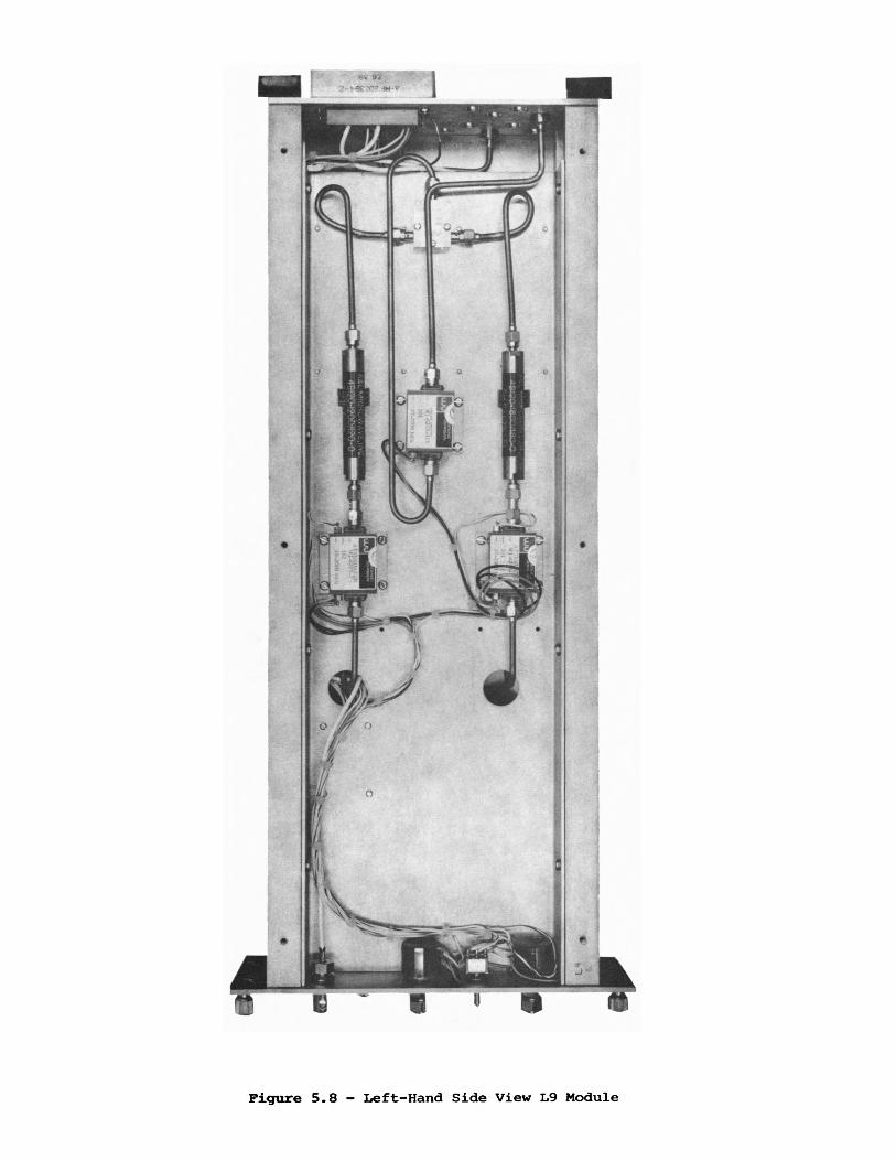
Figure 5.8 - Left-Hand Side View L9 Module


6.0 L10: CENTRAL LOCAL OSCILLATOR TRANSMITTER - REVISION C
6.1 Modifications and Reasons - Reference Block Diagram D13230B8 (Fig. 6.1)
Description of Modification
1. To Revision B:
Delete (a) 6 dB directional coupler
DC-1 (BOM: Item 23) (b) two 600
MHz BPFs FLl and FL5 (BOM: Item
21) and (c) associated RF cables.
2. To Revision C:
(a) Replace Amplica amplifier
(type 200 LSM) by a combination
of an attenuator AT3 (nominal
2 dB) and Watkins-Johnson
amplifier AR2 (nominal gain =
19 dB) such that the net gain
is 17 dB at input signal of
- 6 dBm at each of 1200 and
1800 MHz (i.e., total input
power = - 3 dBm; total output
power = + 14 dBm).
(b) Delete + 20 V regulator
assembly.
(c) Install 6 dB pads between
RF port of each modulator
(MlJ mixer) and 2-way power
combiner DC-3.
Reason for Modification
600 MHz + f (Where s
f = 19.2 Hz) instead s
of the 600 MHz is required
by L14's in view of new
phase detectors in L11C
employing digital techniques.
Therefore, all this
circuitry is unnecessary.
To replace amplifier having
excessive power consumption
and gain by a lower level
amplifier to get a better
phase-stability.
+ 20 V no longer required
in the module.
To improve isolation between
1200 and 1800 MHz modulators
and get appropriate output
levels.
6-1

8M.
f i V p e w s w - j t v f i ' x i
c. / 0 ?! AL>1£[) A - O TO C«<>V/.) «V '
D • - v t y * * IV 1 1 * .0 K X T K N t lV K L V
E <i-D 77 k * .T £ V Z t v * - ^ ,
3 . t * A 5 5 Y C > W < 5 B ! 3 ? 3 0 P > 3 Z , S O M A I 3 Z 3 & S Z I , S C H E M A T I C D W G B I 3 Z 3 0 3 5
« - A 5 S Y P Y / 3 e / 3 2 3 0 P 3 3 , B O M f i ! 3 Z 3 0 Z Z Z t S C H E M A T I C C M /t S C I 3 Z 3 0 S 7
- * * * = A S S Y P W G 0 t 3 Z 3 O P Z C > , O C X S A I 3 2 3 0 Z I 4 , S C H E M A T I C & M S B I 3 Z 3 0 S Z4 . J / 7 . J / 3 B K J C O K I F R O K I T P A N E L5 . "—ARROW MOICATES SIGNAL FLOW6.
D
F L 5 . . .
FIGURE 6.1
1--------- ITEM NUMBERS PER DOM AI3Z30Z.Q------------------ R E F p e S IG PER lECe N O -315 4 N R A O OPEC.
7. * * # + » ADJUST TO C,IV£ A JTFM tA TO H * A M P L IF IE R MET C,4tN O f !7 d & A T CSV ELS S H O tV N .
UNLESS OTHERW ISE SPEC IF IED DIMENSIONS ARE IN INCHES totf«Amrt **u.ri aI PiACt PfCMAit I ai*>: ft1PVACI PfCWALl'.XX* £I or mM.% *
MATERIAL:
LIO CEK/reAL LO. TRANSMITTER
BLOCK DIAGRAM
NATIONAL RADIO ASTRONOMY
OBSERVATORY
:^ r ,D (3 2 3 0 B a ]^8 1

(d) Change resistor R12 from 200
Q to 620 ft in 5 MHz Modulator
Driver.
6.2 Drawings Effected
An updated list of drawings, bills
is enclosed. The drawings effected are
Block Diagram
RF Interconnections
BOM:
BOM; + 20 V Regulator
Schematic: + 20 V Regulator
Rack D Wire List
To provide adequate adjust
ment range for output
1200 MHz carrier with modified
RF input to L port of the
modulator.
of materials (BOM's), etc.
D13230B08 Rev. E
D13230B18
A13230Z08
A13230Z21-L10 - Delete
B13230S05-L10 - Delete
A13050W2
6-2

6.3 Input Output Connections
J7 JlO J8 o J2
J9 O J3 OO JIO o J4
Jll o oJI3
O
JI5o
JI2oJ I4oJ16o
PI
_rrJ
CONN FUNCTIONJlJ2J3J4J7J 8 + 8.5 ± 1 @ 5 MHz InDut
J 9JIOJllJ 12J13 1.2 & 1.8 GHz -6 (-3) ±1.5dBm Input
J 14J 15 1.2 & 1.8 GHz -28.5(-25.5)±l.5dBm C
J 16
LEGEND: No paranthesis - Each L.O. Carrier
Paranthesis - Total L.O. Power
DOUBLE WIDE MODULE ( R E A R VIEW )
+
© ~ © © fes) £3)
© © ©
© © © ©~© ©s©© I ©©s ©0 ^ © ^ ©
© ©© ® ©
PI (REAR VIEVPI
PIN FUNCTION WIRE COLOR PIN FU N CTION WIRE COLOI I 222 I 2 3
2 425
5 Idata in ttl 1 Co-axial, RG-174/L 2 56 |l200MHz Carrier on TTL ) 277 | 2 8 - 2 8 VDC GREEN8 29 + 2 8 VDC GREY
3 0IO | 4 -5VDC | ORANGE 31II | — 5 VDC BROWN 3 212 | 3 313 3 4 PY/R. GROUND BLACK14 3515
15 4 - 1 5 VDC RED 3717 —15 V DC | YELLOW 3813 3 919 4 0
2 0 | 4121 42 HIGH QUAL. GROUND
INDICATES A FUNCTION NOT FOUND IN TH!S MODULE.
6-3

6.4 Central L.O. Transmitter Rev. C (L10C) Module List of
Drawings, BOM's, etc.
Block Diagram
5 MHz Modulator Driver Schematic
Data Modulator Driver Schematic
Bills of Materials
Central L.O. Transmitter
5 MHz Modulator Driver
5 MHz Modulator Driver PC Board
Data Modulator Driver
Data Modulator Driver PC Board
Assembly Drawings
Not Available
Printed Circuit Boards, etc.
5 MHz Modulator Driver
PC Board
Data Modulator Driver PC Board
Module Wire List
Module RF Inter Connection
Diagram
D13230B08
(see B13230S02Fig. 6-2)
C13230S07
A13230Z08
A13230Z14
A13230Z15
A13230Z22
A13230Z23
Art Work
B13230AB10
B13230AB08
SilkScreen Mechanical
C13230M45
C13230M56
A13230W08
D13230B18
Mechanical
Module Guide
Partition Plate
Panel, Rear
Cover, Perforated
Bar Support Top and Bottom-Left
Bar Support Top and Bottom
Panel, Front
Right & Left Side Plates
B13050M04
D13230M64
C13210M04
C13050M22-1
B13230M36
B13050M23
B13230M34
B13050M18
6-4

ZZ-OT 9N
tNH
»a
4-/5
DC A R R IE R
LEVEL f?4 CW ,K
C S/5MFfe0V r ^ ’ H
M » n ? M/V* |!.0«, r IL ‘ MOD MOU\
REV. DATE drawn dv APPRV*0 BY Of SCRIPTlUN
A /-JO-70 CAT: V iS S a O Q " W AS "UP^BQ O"
8 3-tc-7g CMC: R !2 M S e o o sx.
c in-78 CHG : TITLC WV*S 5 MHl DRIV£R SCHEMATIC.
i w I ^|____Y _____I FR0 N T M L
[t t I .
!(A/p(/y i
YW M O DULATO fZ] • . J4 I
B
I— 1! J2 ‘
KJOTES:I.UAJLESS OTHERWISE SPECIFIED:
A. ALL RESISTOR VALUES A R E ! U O H M S « t / 4 W
0. ALL CAPACITOR VALUES A ZE iN M IC R O FA R A D 5
Z, BRACKETED COMP0KJEK/T3 /1FET LOCATED O N B 13Z 3Q R 2 G
LAST COMPOK/EUT DESKS USEDC R c e Q L J U$ /£ 2 ( Z 4 (
A /3 2 3 0 Z /SNEXT ASSY USED ON
3
UNLESS OTHERWISE SPECIFIED DIMENSIONS ARE IN INCHESTOltAAMCES: ANGLES ±3 PLACE OECIMALS (.XXXI: ±2 PLACE 0EC1MAL! (.XX): ±1 PLACE DECIMALS (.X): ±
MATERIAL:
FINISH:*
1A1
\UO CENTRAL LO • t z a k is m t t e z
5 N\H-z.L M O D U LA TIO N D R I V E R
S C H E M A T I C
JHEETNUMOER
NATIONAL RADIO ASTRONOMY
OBSERVATORYCHARLOTTESVILLE. VA. ?W 01
APPROVIU BY
DRAWINGNUMBER &/9230SZ |«».g
1
OATl /t,4 r * l i
ZJL

Data Modulator Driver 5 MHz Modulator Driver Terminal TurretData Modulator Filter End Plate Mixer Mounting Brackets
B13230M27, 29, 30 B13230M46, 47, 48, 49 B132 30M98 B13230M38 B132 30M65
6-5

6.5 Bills of Materials (L10C)
6-6

V L A D A T A L I S T I N G
MODULE: 1 1 0 P RO JE C T NO. 1 3 2 4 0 ORAWlNG N O . : A 1 3 2 3 0 2 C 8DATA S F T : CE NT RAL LO TRANS MITTE R BOM: CENTRAL L C TRANSMITTER 0
MOO-Q/S- Q/N DESCR VALUE MFG. PART NO. MANUFACTURER ITEM# BOM# D F S C R I P T I C N COST
LIO NST A1 32 3 0Z C 8 NRAO 1 A 1 32 3 0 Z 0 8 CENTRAL LC TRANSMITTER 0 0 . 0 0L 10 4 MPM R13050M04 NRAO 2 A 1 3 2 3 0 Z 0 8 GUIDE Z 0 . 2 0L 10 1 MPM D13230M64 NRAO 3 A 1 3 2 3 0 Z 0 8 P A R T I T I O N P LATE M 3 5 . 9 3110 I MPM C13210MQ4 NRAO 4 A 1 3 2 3 0 Z 0 8 P A N E L » REAP F 1 5 . 9 3L 10 2 MPM C1 3 0 5 0 M 2 2 - 1 NPAO 5 A 1 3 2 3 0 Z 0 8 COVER, PEPF OP. ATFD K 1 . 3 8L I 0 3 MPM B 13230M65 NRAO 6 A1 32 3 0 Z 0 8 MIXER MOUNT M 3 . 3 0L IO 2 MPM B13230M36 NRAO 7 A 13230Z 08 BAP SUP TCP C BTM L E F T G 1 6 . 91LIO 2 MPM B13050M23 NRAO 8 A1 32 3 0 Z 0 8 BAR, S U P . TOP C BOTTOM G 1 3 . 4 6LIO I MPM B13230M34 NRAO 9 A 1323QZ08 P AN E L , FRCNT A 7 5 . 0 0LIO 2 MPM K C - 1 9 - 1 53 KINGS 10 A 1 3 2 3 0 Z 0 8 CONNECTOR, PNL BNC 2. 35LIO 2 MPM B 13050M 1 B NRAO 12 A 1 3 2 3 0 Z 0 8 RIGHT C L E F T S I C E P L ATE S H 8 . 7 8LIO 08 H SLWS 4 - 4 0 HW 15 A 1 3 2 3 0 Z 0 8 S P L I T - L O C K WASHER SS 0 . 0 2LIO 1 NSA A 1 3 2 3 0 Z 14 NRAO 16 A 1 32 3 0 Z 0 8 FAST PUL SF MODULATOR 0 0 . 0 0LIO I NSA A 13 23 0Z ? ? NRAO 17 A 1 32 3 0Z 0 B DATA MCOULATCP 0 0 . 0 0LIO 02 M 01 Ml J WATKINS JOHN 18 A 1 3 2 3 0 Z 0 8 M I X , D 8 L BAL OC -I GHZ SMA CCN 7 3 . 0 0LIO M 02 Ml J WATKINS JCHN 18 A l 3 2 3 0 Z 0 8 M IX ,OP L BAL C C - l C h Z SMA CCN 7 3 . 0 01.10 1 FL 03 4 B ] 2 0 - 1 8 0 0 / 1 2 0 - 0 KCL MICROWAVE 19 A 1 3 2 3 0 Z 0 8 F I L T E P , T U B U L A R BF 4 5 . 0 0LIO 1 CL 02 48 1 2 0 - 1 2 0 0 / 1 2 0 - 0 KCL MICROWAVE 20 A1 32 3 0 Z 0 8 F I L T E R , T U B U L A R BP 4 5 . 0 0LIO AT 02 F P 8 7 - 0 6 TEXSCAN 21 A 1 3 2 3 0 Z 0 8 60B ATTENUATOR 3 5 . 0 01.10 02 AT 01 F P B 7 - 0 A TEXSCAN 21 A132 30Z 08 6DB ATTFNL'ATOR 3 5 . 0 0LIO 2 PD 02 2 04 93 OMN I- SP ECTRA 22 A 1 3 2 3 0 Z 0 8 POWER DVDR , ?. WAY , 1-2GHZ 1 2 6 . 0 0LIO PD 03 2 0 4 9 ? OMNI- SP5 CTRA 22 A 1 3 2 3 0 Z 0 8 POWER 0 VOP, 2 WAY, 1-2GHZ 1 2 6 . 0 0LIO I PL 04 4 B 1 2 0 - 1 5 0 0 / 1 GOO-O KCL MICROWAVE 25 A 1 32 3 0 Z 0 8 F I L T E P , TUBULAR BP 4 5 . OCL IO I AR 02 6 2 0 3 - 3 1 3 WATKINS JCHN 26 A 1 3 2 3 0 Z 0 8 SPFC A1323CN4 2 8 2 . 0 0H O I P 2 0 4 1 8 6 - 5 AMP S P E C IND 27 A 1 3 23 0 Z 0 8 B L O C K , P I N 42 MIXEC 1 . 6 8LIO 1 P 2 0 2 3 9 4 - 2 AMP S P CC IND 28 A1 32 3 0Z 0 8 HOOD, P I N ( 42 ANO B.C BLOCK) 0 . 8 7LI O 03 J O MQ - 30 43 - 75 OMNI- SPECTQA 29 A 1 3 2 3 0 Z 0 8 JA CK ,B l . KHO PF MCLNT 1 41 SR 1 . 5 0LIO 4 P O S M - 5 3 1 - 3 OMNI—SP ECTR A 30 A 1 3 2 30 Z0 8 PLUG PT ANGL R G i e e 3 . 5 7LIO 02 P OSM-218 CMNI— SPEC TR A 31 A 1 3? 3 CZOB ADAPTE R, ST RGHT Pl lJG/ PLUG 4 . 5 6LIO 8 W U T - 1 4 1 A UNIFORM TUBES 32 A 132 3 0Z 08 C A B L E , R F S E M I R I G I C 0 . 4 5LIO 15 o 0 S M - 2 0 1 - 1 A O MN I- SP ECTRA 33 A 1 3 2 3 0 ZC 8 CONNECTOR, PLUG 141SR 0 . 8 5LIO 2 P nsM-20i-i OMNI -SP ECTRA 34 A 1 3 2 3 0 Z 0 8 CONNFCTOR ,PLUG 1 4 I S R 0 . 9 4H O 1 NSA A 1 3230Z 2 1 NRAO 35 A 1 3 2 3 0Z 08 P O S I T I V E VOLTAGE REGULATRO 0 . 0 0110 DSH D 1 3 2 3 0 B 0 8 NP.AO 36 A1 32 3 0Z 0 B BLCCK DIAGRAM 7 O.OCL IO 2 P 2 0 1 1 4 3 - 5 AMP S P E C IND 37 A 1 32 3 0 Z 0 8 COAX P IN 2 . 4 8LIO 4 P 2 0 4 1 8 8 - 1 AMP S P F C IND 38 A 1 32 3 0 Z 0 8 CONTACT, PIN 0 . 2 3LIO 2 P 203*164-6 AMP S P E C INO 39 A 1 3 2 3 0 Z 0 8 GUI DE SOCKET 0 . 2 1LIO 1 P 2 0 0 8 3 3 - 4 AMP S P F C IND 40 A 13230Z0.8 GUIDE P I N 0 . 2 31.10 1 P 2 0 2 5 1 4 - 1 AMP SPE C INO 41 A 1 3 2 3 0 Z 0 8 GROUND GUIOE PIN 0 . 4 2LIO DWW- A1 3230W08 NPAO 4 3 A 132307 08 CENTRAL LC TRANSMITTER 8 0 . 0 0LIO 04 H HNS 4 - 4 0 HW 50 A1 3? 3 0Z08 HEX NUT, SS 0 . 0 2LIO 03 H PHS5 6 - 3 2 X 0 . 2 5 0 HW 51 A 1 3 2 3 0 Z 0 8 PAN HEAD 5 L CT T EC SS 0 . 0 2LIO 4 H PHSS 6 - 3 2 X C . 3 7 5 HW 53 A 1 32 3 0 Z 0 8 PAN HEAD StOTTFD SS 0 . 02110 08 M PHSS 6 - 3 2 X C. 750 HW 54 A 1 3 2 3 0 Z 0 8 PAN HEAD S LCT TF D SS 0 . 0 2LIO 06 H PHSS 2 - 5 6 X 0 . 5 0 0 HW 56 A 13230Z 08 PAN HEAD SL CTTF D SS 0 . 0 2LIO 16 H FHS S 6 - 3 2 X 0 . 3 7 5 HW 58 A 1 3 2 3 0 Z 0 8 FLAT HEAO S L C T T E C SS SCREW 0 . 0 2LIO 2 H HSHS 6 - 3 ? X 0 . 2 5 0 HW 59 A 13 ? 3 OZ 08 H E X - S C C K E T HC SLOTTE D SS 0 . 0 2L IO 4 H 4 7 - 1 0 - 2 0 4 - 1 0 SOUTHCO 60 A13230ZOB F A S T N E R , C A P T I V E 0 . 6 7L IO 04 H M12-A KCL MICROWAVE 61 A1 3 2 3 0 Z 0 B MOUNTING CL I F 0 . 0 5110 01 H 1 4 1 1 - 4 H H SMITH 62 A13230Z OB L U G , T E R M I N A L LOCK 0 . 1 5
+ * * T P T . U C O S T * 1 1 68. 00


MODUlF: L10OATA S FT | CENTRAL 10 TPANSMTTT5&
MOO-C/S -0/M OF SCR VALIIF MFG. PART NO.
L i O NS A A 1 3 2 3 0 Z 14L I O 1 MPN B13230M3PL I O 1 Mt>N R13230M30L IO I MPN B13 23 0M2 91.10 1 MPN R13230M27L I O 8 H PHSS 4 - 4 0 X1 1 0 8 H FHSS 4 - 4 0 XL IO 1 MPN B13230M48110 1 MPN B 13230M47L I O I NS A A 1 3 2 3 0 Z 15L I O 02 C 08 0 . 0 0 1 U F F B 3 RI Q F 10 2 WL I O C 09 O. OOI WF F B 3 B 1 0 * 102WL I O 1 F 01 1 5 8 7 - 1L I O F B 1 3230M98L I O 4 J 01 OSM-2111 10 J 03 OSM-211L I O J 04 OSM-211L I O J 02 OSM-211H O DSH B I 3 2 3 0 S 0 2
V L
. 5 0 0
. 3 7 5
A D A T A L I S T I N G
PHOJECT NO. I 1 M 0 DR AWING NO.* A 1 3 2 2CZBOMt F AS T PUL SF MCCULATOR 0
1ANIIFACTURFR IT EM# BOMtf D E S C R I P T I O N COST
NPAO 1 A 1 3 2 3 0 2 14 F AST P U L S E MCDULMCR 0 0 . 0 0NRAO 2 A1 32 3 0Z 1 4 DATA F I L T E R ENO PANEL J ft. 12NRAO 3 A 1 3 2 3 0 Z 14 R E C F I V F R CATA A M P L I P I E P J 3 . 7 1NPAO 4 A 1 3 2 3 0 Z1 4 R E C E I V E R CA T A A M P L I F I E R J 6 . 7 2NRAO 5 A 1 3 2 3 0 Z 14 R E C E I V E R CATA AM PL I F I F R J 2 . 7 3
HW 6 A 13230Z 14 PAN HEAD SLCTTEO ' S 0 . 0 2HW 7 A1 32 3 0Z 1 4 FLAT HEAR S L CT TE O SS SCREW 0 . 0 2
NPAO 8 A 1 3 2 3 0 Z 14 5 MHZ D R I V E R J 0 . 0 0NRAC 9 A 1 3 2 3 0 Z 14 5 MHZ D R I V E R J 0 . 0 0NRAO 16 A 1 3 2 3 0 Z 14 PC BCARP FAST P UL SE MOC 0 0 . 0 0SPFC CONTROL 17 A 1 3 2 3 0 Z 14 CAPACITOR . F E E O T H P L SCREW MT 0 . 6 6SPEC CONTROL 17 A 1 3 2 30 Z1 4 C A P A C I T O R , F E E C T ^ R U SCRFW MT 0 . 6 6k e y s t o n e 18 A 1 3 2 3 0 Z 14 T F R M I N A L t T U P P F T . 1 2 5 4 - 4 0 T H D 0 . 0 9NPAO 18 A 1 32 3 0 Z 1 4 TERMINAL f TURRET PCD N 0 . 0 0OMNI- SPECTRA 19 A 1 3 2 3 0 Z 1 4 JACK BLKHC FTTHPU 2 . 1 5CMN I - SPECTRA 19 A 1 32 3 0 7 1 4 JACK BLKHO FDTHRU 2 . 1 5OMNI- SPECTRA 19 A1 3 23 0Z 1 4 JACK BLKHC FCTHPU 2 . 1 5OMN) I - SPECTRA 19 A 1 3 2 3 0 Z 14 JACK BLKHD FOTHRL' 2 . 1 5NPAO 20 A 1 3 2 3 0 Z 14 5 MHZ D R IV E R SCHEMATIC 2 0 . 0 0
* * ♦ t o t a l COST= 3 1 . 6 1 * * *


V I A D A T A L I S T I N G
MDOULc : L I O P ROJECT NO. 1 32 4 0 ORAWING N O . : A 1323CZ I 5d a t a S E T : c e n t r a l LO TRANSMITTER ROM: PC BOARD FAST PULSE MOD 0
mod- o / s - 0/M OESCP VAUJF MFG. ° A RT NO. MANUFACTURER ITEM# BOM# D E S C R I P T ICN C C ST
L i e NS A A 1 3 2 3 0 2 I 5 NRAO 01 A 132 3 0 Z 15 PC BOARD FAST P U t S E MOD 0 0 . 0 0110 01 EPCO C I 3 2 3 0 M 4 5 NRAO 02 A1323 0715 FAST P U L S E MCD OR CIAG 6 3 . 15u o 01 R 01 1 . 2 K RCP07 1 2 2 - 5 S 03 A132307. 15 R E S I S T O R 1/4V* 0 . 0 *1 10 02 R 02 3 0 0 . 0 P CP 0 7 3 0 1 - 5 S 04 A 132 30Z 15 R E S I S T O R l/4V< 0 . C 61 10 P 05 3 0 0 . 0 RC P07 3 0 1 - 5 S 04 A1 32 3 0Z 1 5 R E S I S T O R 1/4V* 0 . 0 6110 01 P 03 3 . 0 K RCP07 3 0 2 - 5 S 05 A 1 3 2 3 0 Z 15 R E S I S T O R 1/4V 0 . 0 6L 10 01 P 04 1 . 0 K 3 3 3 9 P - 1 - 1 0 2 BOURNS 06 A 1 3 2 3 0 Z 15 P O T , C E R M E T , 4 T U P N , ♦-10% 2 . 5 CL 10 01 P Oft 2 . 0 K RCP07 2 0 2 - 5 S 07 A 1 3 2 3 0 Z 15 R E S I S T O R 1 / 4 V* 0 . 0 6L 10 01 0 07 1 . 0 K RCP07 1 0 2 - 5 S 08 A 1 3 2 3 0 Z 15 R E S I STOP 1/4V* 0 . 0 6LIO 01 P 08 5 0 . 0 3 3 3 9 P - 1 - 5 0 0 BOURNS 09 A 1 32 3 0 Z 1 5 P O T . C E P M E T , 4 T U R N , ♦ - 1 0 ? 1 . 9 f t110 04 P 09 2 0 0 . 0 P CP 07 2 0 1 - 5 S 1C A 1 3 2 3 0 Z 15 R E S I S T O R 1 / 4 V» 0 . 0 6LIO P 10 2 0 0 . 0 RCR0 7 2 0 1 - 5 S 10 A 1 3 2 3 0 Z 15 R E S I S T O R 1 / 4 W 0 . 0 6LIO P 11 2 0 0 . 0 RCP07 2 0 1 - 5 S 1C A 1 3 2 3 0 Z 15 R E S I S T O R 1/4V» 0 . 0 6LIO P 12 2 0 0 . 0 PT.R07 2 0 1 - 5 S 10 A 1 3 2 3 0 Z 15 R E S I S T O R 1/4V< 0 . 06LIO 01 C 01 9 1 0 . 0 PF DM 1 5 9 1 1 J ARCO 11 A 1 3 2 3 0 Z 1 5 CAPACITOR , MICA 500VCC 0 . 12LIO 01 f. 02 1 5 . 0 UF C S 1 3 8 F 1 5 6 K SPRAGUE 12 A 1 3 2 3 0 Z 15 CA P AC I TO R ,T A NT AL LM 20V0C 0 . 2 4LIO c 04 1 . 0 IJP 8 1 3 1 - 0 5 0 - 6 5 l - l 0 5 M E R I E 13 A 1 3 2 3 0 Z 15 CA PACITOR, MONOL YTHI C 50V0C 1 . 2 3110 02 r 03 1 . 0 UF 8 1 3 1 - 0 5 0 - 6 5 1-105M E R I E 13 A 1 3 2 3 0 Z 15 CA PACITCR, MCNOLYT HTC 5 0VCC 1 . 2 31.10 02 C 05 1 5 0 . 0 PF 0 M 5 1 1 5 1 J APCO 14 A 13230Z 15 CAPAC I T OR ,MI CA 2CCV0C 0 . 13LIO C 06 1 5 0 . 0 PP DM51151J ARCO 14 A 1 3 2 3 0 Z 1 5 CAPACITOR , MICA 3CCVDC 0 . 13110 01 c 07 1 5 0 0 . 0 PF DM19152 J AOC0 15 A13230Z 15 C A P A C I T O R , M I C A 5CCVPC 0 . 1 5LIO 01 Q 01 MPS3640 MOTOROLA 16 A1 32 3 0Z 1 5 T RA N S I S T O R , S M SIGNAL 0 . 1 3L IO 01 U 11 L H 0 0 33 C G NAT SEMICOND 17 A 1 3 2 3 0 Z 15 A M P L I F I E R , C P FET 1 4 . 4 9110 01 L 01 1 . 0 UH 9 2 3 0 - 2 0 M IL L E R 18 A132 30Z 15 C H O K E , P F NICRC VINATUR E 0 . 3 0LIO 01 L 02 1 0 . 0 UH 9 2 3 0 - 4 4 M I L L E R 19 A1 32 3 0 Z 1 5 CHOKE,10MH 10? 0 . 6 0L IO 01 CP 01 I N 9 3 7 B MOTOROLA 20 A 1 3 2 3 0 Z 15 D I O D E , R E F TC 9 . 0 V 4 . 5 8LIO 01 CP 02 A 2 ' 8 0 0 AERTECH 21 A1 32 3 0Z 1 5 D I O D E , S H O T T K E Y 1 . 0 5LIO 01 X 3 - L P S —B CI NCH 22 A 1 3 2 3 0 Z 1 5 S O C K E T , T R A N S I S T C R T 0 - 5 , T 0 - 1 8 0 . 1 2L IO 01 X MP121 OOS ROB NUGENT 23 A 13 2307.15 S O C K E T , 12 P I N TO-fl SQUARE 0 . 2 8LIO DSH B 1 3 2 3 0 S 0 2 NRAO 24 A1 32 3 0Z 1 5 5 MHZ D RI VE R SCHEMATIC 2 0 . 0 0LIO E pC A B l 3 2 3 0 A 8 1 0 NpAO 25 A13230Z 1 5 5 MHZ D P I V E R 4 0 . 0 0
* * * TOTAL CO ST * 3 3 . 0 1 ♦ * *


V I A D A T A L I S T I N G
MODULE: L I OP U A S E T : CENTRAL LO TRANSMfTTER
P RO JE C T NO. 1 3 2 4 0 DRAWING N O . : A 1 3 ? 3 0 Z 2 2 BOM: OATA MCCULATCB
MOO-Q/S -0/M DESCP VALUF MFG. PART NO. MANUFACTURER ITEM#
LIO NS A A 1 32 3 0Z 22 NRAO 1LIO 1 MPN B13230M38 NRAO 2LIO 1 MPN B 13 230M30 NRAO 3LIO I MPN B13230M 29 NRAO 4LIO 1 MPN R13230M27 NRAO 5LIO I MON B 13 23 0M4 6 NPAO 6Li O 1 MPN B13230M49 NRAO 7L I O 8 H PHSS 4 - 4 0 X 0 . 5 0 0 HW 8110 8 H * HSS 4 - 4 0 X 0 . 3 7 5 HW 9L I O 3 J 01 HSM-211 OMNI- SPECTRA 17L IO J 02 OSM-211 OMNI- SPECTRA 17LIO J 03 OSM-211 OMNI -SP ECTRA 17L 10 1 E 01 1 5 8 7 - 1 KEYSTONE 18LIO 1 f. 01 O . O O I U F F B 3B 10 F10 2W SPEC CONTROL 19L iO r. 12 0 . 0 0 1 U F F B 3 R 1 0 p l02W S PE C CONTROL 19LIO I NS B A 132307 23 NRAO 20110 OSH C 13 2 3 0S 07 NRAO 21
BOH# D E S C R I P T I O N
A1 32 3 0Z 2 2 DATA MQDULATCRA 1 3 2 3 0Z 2 2 DATA F I L T E P EKO PANELA 1 3 2 3 0 Z 22 R E C E I V E R DATA A M P L I F I E RA1 32 3 0Z 2 2 R E C E I V E R CATA A M P L I F I E RA 13230Z 22 R E C E I V E R CATA A m i ^ I E RA 1 32 30Z 22 DATA MOD DRVR ENP PANELA 1 32 3 0Z 2 2 DTA MCD OPVP S I C E PANELA 1 3 2 3 0 Z 2 2 PAN HEAO SLOTTED SSA1 3 230 Z22 FLAT HEAD S L C T T E C SS SCREWA 1 32 3 0 Z 2 2 JACK BLKHO FDTHRUA 1 3 2 3 0 Z 2 2 JA CK BLKHO FQTHRUA 1 3 2 3 0 Z 2 2 JACK f lLKHC FDTHRUA 1 3 2 3 0 Z 22 T E R M I N A L , TURRET . 1 2 5 4 -4 0 THDA1 32 3 0Z 22 C A P A C I T O R , FEEOTHRU SCREW MTA 1 3 2 30 72 2 C APAC I TOR ,FFFDTHRL' SCREW MTA1 32 3 0Z 2 2 MOD BOARD 0A1 32 3 0Z 2 2 DATA MODULATCR DRIVER 2
COST
O.OC8 . 1 23 . 7 16 . 7 22 . 7 3 0.00 0.00 0.02 0.022 . 1 52 . 1 52 . 1 5 0 . 0 9 0.66 0.66 0.00 0.00
* ♦ * TOTAL COST* 2 8 . 8 0 * * *


V I A O A T A L I S T I N G
MODULF: L I O P R O JE C T NO. 1 3 2 4 0 DRAWING N O . : A 1 3 2 3 0 Z 2 3OATA S E T : CENT RAL LO TRANS MITTE R BOM: KCD BOARD 0
Mnn- Q/S-O/M DESCR v a l u e MPG. PART NO. MANUFACTURER ITEM# BOMtf O E S C R I P T I C N COS*
1.10 NSA A1 32 3 0Z 23 NRAC 01 A 1 32 3 0Z 23 MOD BOARO 0 O . o ci r o 01 EPCD C 1 32 30 M5 6 NRAO 02 A 13 2 3 OZ 2 3 DATA MODULATCR C P I V E R 6 0 . 0 0n o 01 p 01 6 2 0 . 0 PCR07 6 2 1 - 5 S 03 A 1 3 2 30 Z 23 R E S I S T O R I /4V» O.Ofc110 01 P 02 3 0 0 . 0 RC R0 7 3 0 1 - 5 S 04 M 3 2 3 0 Z 2 3 R E S I S T O R l / A h O.Ofc110 01 R 03 2 . 0 K RCR07 2 0 2 - 5 S 05 A 1 32 3 0Z 23 R E S I S T O R l/4fc 0 . 0 6H O 01 R 04 5 . 0 K 3 3 3 9 P - 1 - 5 0 ? BOURNS 06 A 1 3 2 3 0Z 2 3 P O T . C E R M E T , 4 T U R N , * - 1 0 ? 1 . 9 8L IO 01 R 05 1 0 . 0 K RCP07 1 0 3 - 5 S 07 A1 32 30Z 23 R E S I S T O P 1/4X 0 . 0 6L I O 01 R 06 3 9 0 . 0 R C P 07 3 9 1 - 5 S 08 A 13230Z 23 R E S I S T O R I / 4 V. 0 . 0 6110 01 P 07 2 . 0 K 3 3 3 9 P - 1 - 2 0 ? BOURNS 09 A1 32 30Z 23 P O T . C E P M E T , 4 T U R N , * - 1 0 * 1 . 9 RL IO 01 P OR I . 5 K RCP07 I 5 ? - 5 S 10 A 13230Z 23 R E S I S T O R 1/4U 0 . 0 61 10 01 f> 09 2 4 0 . 0 R C P07 2 4 1 - 5 S 11 A 132 30Z 23 R E S I S T O R l/4Vi 0 . 0 6LIO 01 R 10 3 3 . 0 RCR07 3 3 0 - 5 S 12 A 1 32 3 0Z 2 3 R E S I S T O R 1/4V* 0 . 0 6I 10 01 P 11 5 1 0 . C RC P07 5 1 1 - 5 S 13 A13230Z 23 PF S I STOR 1 / AV» 0 . 061 10 03 P 12 2 0 0 . 0 R C P07 2 0 1 - 5 S 14 A132 30Z 23 RESI STOP. 1/4 to 0 . 0 6L I O n 13 2 C 0 . 0 PCP07 2 0 1 - 5 $ 14 A 13 230 Z23 RF S I ST OR 1/4W 0 . 0 6L I O p 14 2 0 0 . 0 P C P 0 7 2 0 1 - 5 S 14 A1 32 30Z 23 R E S I S T O R 1/4 W 0 . 0 6L I O 01 R 15 1 0 0 . 0 RCR07 1 0 1 - 5 S 15 A 1 3 ? 3 0 Z ? 3 R E S I S T O R 1/4W 0 . 0 6L I O 01 R 16 5 . 1 K RC R 07 5 1 ? - 5 S 16 A1 32 30Z 23 R E S I S T O R 1/4V. 0 . 0 6LI O 01 C 02 1 5 . 0 IJP C S 1 3 R P 1 5 6 K SPRAGUE 17 A1 32 3 0Z 2 3 CAPACITOR,TANTALUM 20V0C 0 . 2 4L I O 01 c 03 1 0 . 0 PF C M0 4 C D l 0 0 J 0 3 ARCO 18 A 1 3 230 Z23 CA PAC IT OR MICA 500VVDC O . l lL I O 02 r 04 0 . 1 UF flI 2 1 - 0 5 0 - 6 5 l - l 0 4 M F R I E 19 A1 32 3 0Z 2 3 CAPACITOR, MONOL YTHI C 50VDC 0 . 19110 c 05 0 . 1 UF 8 1 2 1 - 0 5 0 - 6 5 1 - 1 0 4M E R I E 19 A132 30Z 23 CA P AC I TC R . MCNCLYTHIC 5CV0C 0 . 1 9L I O 01 c 06 0 . 0 4 7 U F 8 1 2 1 - 0 5 0 - 6 5 1-473M E R i e 20 A 132307 23 C A PA C I T O R , M C N C L Y T H I C 50VCC 0 . 1 6L IO 01 c 07 3 3 0 . 0 PF C M 0 4 F A 3 3 1 J 0 3 ARCO 21 A1 32 3 0Z 2 3 CAPACITOR MICA 5 CCtoVDC 0 . 1 9LI O 01 c 08 1 2 0 . 0 PF C M 0 4 F D 1 2 1 J 0 3 ARCO 22 A 13 2307.23 CA PAC ITOR MICA 5C0V<V0C O . l lI 10 01 c 09 2 4 . 0 P F C M0 4 F 0 2 4 0 J 0 3 ARCO ? 3 A 1 32 30 Z23 CAPACITOR MICA 5CCV»VDC 0 . 1 1L I O c 11 1 . 0 UF 8 1 3 1 - 0 5 0 - 6 5 1 - 1 0 5 M E R I E 24 A 132 30 Z23 C A P AC I T CR . M HN C LY TH I C 50VCC I . 2 3L I O 02 c 10 1 . 0 UF 8 1 3 1 - 0 5 0 - 6 5 1-105M E R I F 24 A 132 30 Z23 C A P A C I T C R .MCNCLYTHIC 50VCC 1 . 2 3L IO 01 c 13 1 5 0 . 0 P c C M 0 4 F 0 1 5 1 J 0 3 APCO 25 AL32 30Z23 CAPAC ITOR MICA 5 CChVOC 0 . 1 1LI O 01 c 14 4 7 CO • 0 PF R 1 2 1 - 0 5 0 - 6 5 1-472M E R I E 26 A1 32 3 0Z 2 3 CAPACI TCR,MON'CLYTHIC 5 0VCC 0 . 1 11 10 01 L 01 4 7 . 0 UH 9 2 3 0 - 6 0 M IL LE R 27 A 132 20Z 23 CHOKE,P.F M IC 0 C MINATURE 0 . 2 81.10 01 L 0 ? 2 ? . 0 UH 9 2 3 0 - 5 2 M I L L E R 28 A1 32 3 0Z 2 3 C H O K E , R F MICRC MINATURE 0 . 5 5L I O 01 L 03 3 . 3 UH 9 2 3 0 - 3 2 M I L LE P 29 A 132 30Z23 C H C K E . P F MICPC * ! NATURE 0 . 4 6L IO 02 C« 01 A 2 S 8 0 0 AERTECH 30 A 132 30Z 23 C I O C E . S H O T T K F Y 1 . 0 5L I O CP 02 A2 SR00 AERTECH 30 A 132 30 Z23 D I O D E , S H O T T K E Y 1 . 0 5L I O 01 CP 03 1M937R MOTOROLA 31 A 1 3 2 30 Z2 3 D I O D E , R E F TC 9 . C V 4 . 5 8L I O 01 u 01 LM318H NAT SEMICONO 32 A 1 32 30Z 23 OP AMP 1 . 9 PL I O 01 u 02 L H0 0 33 C G NAT SFMICCNO 33 A 13230Z 23 A M P L I F I E R , O P F E T 1 4 . 4 9LIO 01 X O P - 5 1 7 8 ROB NUGENT 34 A1 32 30Z 23 S O C K E T , 8 PIN t c - 5 1 . 9 8L I O 01 X MP12100S ROB NUGENT 35 A 1 3 230 Z23 S O C K E T , 12 PIN T 0 - 8 SQUARE 0 . 2 8L I O FtPCA B13 23 0 &B 08 NPAO 36 A132 30Z 23 DATA MOOULATCP D RI VE R 4 3 . 0 0L I O DSH C 1 3 2 3 0 S 0 7 NRAO 37 A1 32 3 0Z 2 3 CATA MOCULATCR CF »V ER 2 0 . 0 0
♦ * * TOTAL C O ST * 3 5 . 3 8 * * *
* * * TOTAL COST FOR MOOULE L I O I S 1 2 S 6 . 8 C * * ♦


7.0 L14: CENTRAL LOCAL OSCILLATOR FILTER - REVISION C
7.1 Modifications and ReasonsDescription of Modification
1. To Revision B:(a) Add a 1200 MHz BPF (4B120-1200/ 120-0 by K and L Microwave, Inc.) and a 20 dB pad between 1200 MHz 4-way power divider DC-2 and RF port of the mixer Z3. Also, add a 1800 MHz BPF (4B120-1800/180-0 by K and L Microwave, Inc.) between 1800 MHz 4-way power divider DC3 and L.O. port of the mixer. See Block Diagram D13230B12 (Fig. 7.1).
(b) Modify output of Buffer Amplifier (A7) as shown below:
OUTPUTMONITOR
Reasons for Modification
The two BPF's have been added to filter harmonics of 1200 and 1800 MHz going to the mixer. The 20 dB attenuator has been put in 1200 MHz path (note 1200 MHz is given to R port of the mixer) to reduce R port input of the mixer so that intermodulation products generated in the mixer are low (at least - 40 dBc compared to the desired product.)
Design change of monitoring 600 MHz round trip phase digitally using 19.2 Hz offset and digital phase detector in new Central L.O. control modules Rev. C (L11C).
7-1


8►r* p*Tt
RCVD 1200 MHz INPUT ^ 0 *0 .5 dBm
-/Od&M
1800 /CO ^ CONTROL MON.
Pt-t v , REMOTE LOOPS' OPEN/CLOSE
PI-30 v , fdOOMHt 0 ERROR
.... 1 . idoo tmYCO
PUdSF ItT.K mno -V RFTTL MI4H » OPEN * P. C. BOARD AFC OUT
n Yl W
je sKCVD 1800 MHz INPUT >
Q tQ .S d & m
1 3 0 0 MH i LO O P-±: OUT OF LOCK INDICATION v_ _ C/U (FRONT PM)\g£
+ Z2J6m<*dB
+ATI m
?MIXER I
Z3 IS
•HOd&M
NOTES’./ . J /, j? .cy tf.u tf < J /5 ARE ON REAR PANEL.I . P I- 42 P/N CONNECTOR3. — ► ARROW /ND/CATES SIGNAL FLOWA. *=A5Sr DWG B/3Z 3OP37, BOM A/3230Z32,SCHEMATIC Dm D/3230S/3. R EV ISED COMPLETELY.
* * - ASSY Dm &/3Z30P33.B0M A!3?30?26. SCHEMATIC DW6 3/3230S/0.«**• ASSY DWG 3/3Z30P40,. BOM A/3230234,SCHEMA TIC DWG 6IX30SI6.**** . ASSY DWG C/3230P39.B0M A/3230131, SCHEMA TIC Dm 3/3230312.***** - ASSY DWG 3/3230P24, 3CM A/3230224, SCHEMATIC DWG 3/3Z30S0, REVISED SLIGHTLY.
5. J!%OSMON FRONT fHNEL6.
iL__ m■ ITEM NUMBERS PER M M AJ3230233. - REF DESIG PER IEEE N0>3JS< NRAO SPEC.
&>tii w ? »TT
ODffn SlGvai IHZO Aooeo r re t f g/
MV. I OATl I IWW 0*»C*1TX*
CRf M
A£ DA n-V; XjocO SPF4&X) -AVOl HO-OIFL L)!T£M 63, iraAWW Xkt6 MKDA 47frM0fi£QUlV(*n)irM6& BPF JgUttiMC/OO-O FIS t7£M<0+.
. PI-23 '</ZOOMHt
YCO OUTPUT Mou n o *
* <J\itOOMHlOUTPUT
B P fO/il6 0 0 / i DO
FU I/s-l&dBM
■MB
OC! m
(o /d 3FP)AOOMUt
<
-3d&M
RMIXER L
____J2
^ J 7 <^600
7£R0CROSSINGDfTfCTOR
♦ e. s * i. eJOm ^#fF MPttr
^ P I-7 -< 6 0 0 * 1 H i
G r o u n d t r ip0 INFORMATION
*101 z. J I5
• < 1300MHl OUTPUT
CRi m<
PI-24 f6 0 0 MM*YCO OUTPUT MONITOR
fI
-<Pt-3A(P0MR6ND)
- <Pb/3 (SIGNAL PONER
FIGURE 7.1UNLESS OTHERWISE SPECIFIED
DIMENSIONS ARE IN INCHESTOLMMCtt AftQLtS ±injctoccaMU<.XM>. *>Pt>etMcawui.uo: ±1 PlACl M W U (.*>: ±
1/LA_T
5 LJ4CENTRAL L.O . 1 F IL T E RC
NATIONAL RADIO ASTRONOMY
OBSERVATORYC»A*LOTTUVILU. VA. 22M
k BLOCK DIAGRAMDRAM BY OAT(Cf-4'73MATERIAL it
AJSZ30i33 FINISH: %-h-isNEXT ASSY USED ON ir ± S . P / 3 2 3 0 3 / 2 K £ ttAil
B
8


2. To Revision C:Replace Phase Lock Loop PC Boards by new design boards and remove 1200/ 1800 MHz 6 -Error Indicator Board (A4). See enclosed description of the new circuit and adjustment procedure.
New Phase Lock Loop Boards contain VCO sweep circuit. The loop filter and lock indication functions have been separated out when input signal is present. However, when the signal not present the lock indication will be given by drifting of the loop integrator to one side.The 1200/1800 MHz <J> -Error Indicator circuit is no longer required to drive the LED's.
7.2 List of Drawings Enclosed
1.2.3.4.5.
Block Diagram Central L.O. Filter (Fig. 7.1) D13230B12Phase Lock Loop PC Board Schematic (Fig. 7.2) D13230S13Zero Crossing Detector Schematic (Fig. 7.3) B13230S26Bill of Material Central L.O. Filter (Fig. 7.1) A13230Z33Bill of Material Phase Lock Loop PC Board A13230Z32
7.3 Phase Lock Loop
7 .3 . 1 Phase-lock loop board - Reference Schematic D13230S13 (Fig. 7.2) The phase-lock loop PC board contains loop DC
amplifier and integrator. Loop out-of-lock indication circuit and VCO sweep circuit. When the VCO output frequency is different from the input reference signal a free running multivibrator output is connected to the input of the loop integrator. This makes the
7-2


8 I 1
+ 15 V
LjO C K IN D IC A T IO N ! T O C O M P U T E R P b (SCC T A B lf A )
•IV OAT( OOMNtT kmtvorr M K*n«l
B U' '7'7 7
HLVIfSED 4 REDRAW N
c . S'
S 01 R-S-»" W A S
VALUE W AS S . ^ K . K-12 W A S 2 .2 K ,n S I WA6 8 2 0 -a WEMOV/fcO R 3 2 ,1=137 ,C I O i C ll
D =>-27-77
AESDED C.15
Ell-Z*77
C I5 WAS 9 1 0 0 pP CIO WAS Cl*5CO-W£ 770711-DS0-*
• « 77c^^9-vsa - ' 7u ^ - 5 o * a
F 3-Vf t
r-vtf.' */7 r<« j j * .*M f. 7<*f, J*J« «X* XfM torfD I f l - r t O K f
«f > M
w 7/tB i e r ♦
TO + I 5 V O— -H 5V E O S
-» 5 V B U *
T O -*>3V O— + 5 V B O *
&NO BU«
M O W
- I 5 V
t . AIL MONITOR/ CONTROL POINTS AMO POWFR SVPPL Y COHNCCTtONS QO 7HAL) FILTER fC C D TNAttS (S P lX T R i/M CONTROL T r r e ) ktOUfSTfO OH $M € L O OF AMR CONN € (TOR R t
O F R E Q . CWRjO Rp i - (see T 4 * tr A )
13 (MODEL C ) u * (M ooei c )
IZOO MHt 1800 MNu 1200 M H i 1 8 00 MH a
0 P I- Z4 P h Z 2 p i - s i PI-JOP I-Z3 p i - a P l-Z i P I - I I
XSMOTr CONTROL P I I Z Phl4- P IS Pl‘ lLOCK INDICATION P l-Z S PJ-ZA P /-S P/ - 9
FIGURE 7.2
NEXT ASSYA)9290?32
USED ON
UNLESS OTHERWISE SPECIFIED DIMENSIONS ARE IN INCHEST o u u m t M m .i l ±I n>et Kcawu IJUOO: * ln>ctoccvAU(Jix)! *I PLACt M C M M JI.IO : ±
MATERIAL
FINISH:
« U 3 / l_ l< 4 L O T R A M 6 'Em i t t e r / c e n t r a l\ L O F I L - T E R
PHASE LOCK LOOP P.C. BOARD SCHEMATIC
ItMAWMGia
NATIONAL RADIO ASTRONOMY
OBSERVATORYc»Muom»vn>Lt. v*. ran RTwTir""-""
DtfiOntOir
ATH*OVtO rr"
8Dt32.~5Q6I I 7
1
■srrr ± 2 2JMT|
e*H"
B


SRUNMG
40-22
24984-1

integrator output to vary in sawtooth fashion and sweeps thG oscillator frequency. When the oscillator frequency is within the pulling range of the loop, the loop should acquire lock and the multivibrator signal to the integrator is cut off.
The output from the phase detector is terminated at the input of the phase-lock loop board by a 51 fi (R26) in series with a 470 pF (C13). It is amplified by the operational amplifier (U2) to ±10 V p-p for a 2ir radian phase change- It can be monitored at <f>-error monitor point- The loop can be opened manually by setting the three position toggle switch Si in open position or by an external +5 V signal at "REMOTE" in the remote position of the toggle switch. The loop open/close function is performed by one section of the dual SPST switch AD7513 (U5). The other section of the U5 is used to connect a free running multivibrator output to the input of the integrator U3 and is controlled by out-of-lock indication circuitry consisting of Ul and U4A.
When a beat signal is present at the input of the phase-lock board, output of the wideband amplifier Ul coupled by C5 to CR4 drives the amplifier U4A. Output of the amplifier U4A is used to connect the multivibrator output to the input of the integrator U3. Output of Ul is AC coupled to the diode CR4 for the following reason.In this type of circuit phase detector current to the integrator has to be larger than the sweep current to acquire lock. The phase detector output amplified by U2 may be such that it compensates the multivibrator output.In that case the phase detector output will vary at the same rate as that of the multivibrator and the loop will not be allowed to lock. Since the multivibrator rate is
7-3

very slow (<1 Hz) , the Ul output to CR4 is cut off by the high pass filter CSRl. This causes to open the switch disconnecting the multivibrator output to integrator and the loop should lock. The multivibrator is made up of U63 and U6D and the time constant is determined by R40 and C12. Also the output of Ul is given to the amplifier U4B through diodes CRl and CR2. When the phase-lock board input exceeds about 40 to 50 mV such that Ul output is able to drive the diodes CRl or CR2 the U4B output will go high and switch 'ON' the LED to indicate that the loop is out-of-lock. Diodes CR3 and CR5 are connected in +15 V and -15 V DC power lines of the MOSFET analog switch AD7513 (U5) to protect it from damage due to transients.
The integrator consists of the operational amplifier U3 and the time-constants are formed by R3 5, R45 and C15.With the phase-lock loop set up properly and in lock the output of the integrator should be close to +4V. The resistors R33 and R31 change the integrator output swing from ±15 V to 0 to -15 V DC as required by the VCO. Also output of the integrator is monitored through a 10 k resistor (R30) and is labeled as *FREQ. ERROR*. When no signal is present at the input of the phase-lock board Ul output is zero and the multivibrator output is not connected to the integrator and thus the integrator output is not sweeped. However depending on the DC offset bias conditions of the operational amplifiers U2 and U3 the integrator will swing to either +ve or -ve extreme (more them 13 V) and stay there. In this case though USD will not come 'ON* to indicate that the loop is not in lock but the integrator output can be used to indicate no signal condition- This is done by computer.
7-4
7. 3.-2 Loop parametersFor the theory of phase-lock loops and terminology
used here refer to Phase-Lock Techniques by F.M. Gardner (John Wiley & Sons, Inc., New York 1966).
To minimize phase difference between the reference and signal a second order high gain integrator was chosen for the loop filter. Also as forced sweep is required for this system the loop parameters were optimized between good lock acquisition and low noise performance.
From the VCO data the mean value of the oscillator AFC port sensitivity is 0.5 MHz/Volt. Further the gain of the DC offset network at the output of the integrator is 0*5. Therefore the VCO gain constant
K = 0*5 x (0*5 x 106 x 2tt rad/Volt) = 1*57 x 106 rad/Volt o
The gain setting of the DC amplifier Ul makes the phase detector output swing of ±10 V for a 2ir radian change. Therefore at zero crossing the phase detector gain constant = 10 V/rad.
*' K = K K = 15*7 x 106 v o D
For best lock acquisition it is desirable to have as large a loop natural frequency (o> ) as possible. However noise and stability considerations force to limit the same. Consider the accuracy with which the loop tracks the input signal and the frequency over which the system will pull into lock. Assume a 0*1% ripple on the power supply tuning the VCO (say about 15 mV in 15 V DC) at 120 Hz. This will cause the VCO to deviate by about 7*5 kHz (500 x 103 Hz/Volt x 0*015 V). From Equations
7 - 5

(4*12) and (4*13) on page 31 of Gardner we get the peak residual phase deviation.
G = AcO'O) /ti) 2 e m n
Where Aoj = peak frequency deviation and u> = modulatingmfrequency. For 0 <0.1 requires to /2tt ~25 kHz. We chose e n•3 radtj /2ir = 35 kHz, i.e. a) = 220 x 10 ---.n n sec
For good lock acquisition characteristics we chose a damping factor of 2 (see Gardner page 48). With the above parameters this will give (i) the pull in range (see Gardner page 45)
Au) /2tt = - 1/3 (D K Hz = (-) * /2x220xl0Jxl5*7xl0b ~ 1 MHz p tt n v tt
and (ii) the lock in range (see Gardner page 43)
Aw /2tt = 2£ u) /2tt = 140 kHz.L n
Essentially these will be limited by the bandwidth of the first op. amplifiers U2. In practice the pull in range may be limited to = 300 kHz.
From Gardner, page 9, Equation (2*10) we can express
K K , o D.M = (----)n T1
-r. K K ** c = 12 . (_ o ^v 2 T,
where Xj = R35-C15 and x2 “ R45*Cl5 in our case. Usingto = 220 x 103 rad/sec and C - 2, we get T, = 320 yS and n 1x2 = 20 yS. For Cl5 = 0*033 yF this gives R35 = 10 kHz and R45 ~ 600 ft.
7-6

7.4 Test and Adjustments
7.4.1 Testing and Adjustments of 1200 and 1800 MHz OscillatorsThe test and adjustment procedure for both 1200 and 1800 MHz
oscillators is similar and we will describe it for only 1200 MHz VCO. For adjusting mechanical tuning of these oscillators allow at least half an hour of oscillator warm-up time.
a) RF output power from the oscillator as measured using a power meter should be at least +22 dBm.
b) Connect the AFC port of the oscillator to a negative voltage power supply through a 10 k resistor. Measure the frequency of the oscillator using output at OMQ jack L3J8 with a spectrum analyzer. Adjust the mechanical tuning of the oscillator so that the frequency change with AFC voltage of zero to -13 V DC swings the oscillator frequency equally on both sides of the nominal frequency.
c) With the AFC port of the VCO still connected to the power supply measure the FM tuning slope of the oscillator. It should be about 0*4 to 0*6 MHz/Volt around -7 Volt at the AFC port.
d) Remove the power supply from the AFC port of the VCO and restore normal connection.
7.4.2 Procedure to Set-up Phase-lock Loop Boards - ReferenceBlock Diagram D13230B12 and Circuit Schematic D13230S13As in the case of adjustment of the oscillators procedure
to set-up both 1200 and 1800 MHz phase-lock loop PC boards are similar. Here we will describe it for 1200 MHz phase-lock board with connections for 1800 MHz phase-lock adjustments in brackets.
a) With L14J3 (L14J2) terminated and U2 gain pot R46 set to maximum adjust U2 DC offset pot R47 so that the
7-7

DC output of the amplifier U2 as measured at '<f>-ERROR' monitor point is within ±100 mV.
b) Connect a 0 dBm signal at 1200 [1800] MHz from L9J12 (L9J13) module to L14J3 (L14J2).
c) Set the toggle switch SI to open position and connecta variable negative voltage power supply through a 10 k resistor to AFC port of the oscillator. Measure the phase detector output beat frequency as measured at the input of the phase-lock board by an oscilloscope. Adjust the AFC port voltage so that the beat frequency is <10 kHz. The amplitude of the beat signal should be about 300 to 500 mV p-p.
d) Adjust the gain pot R46 such that the output of the operational amplifier U2 as measured at the ' <j>-ERROR' monitor point is 20 V p-p. The DC offset should be within ±200 mV.
e) Check that the output of the integrator going to the oscillator is sweeping between 0 and about -13 V at approximately 1 Hz (the multivibrator output frequency rate). Otherwise check the multivibrator output at pin 10 of U6 by a scope. It should be switching between +0*8 V and +5 V at -1 Hz.
f) Remove the DC power supply from the AFC port of the VCO and restore the phase-lock board output to the AFC port of the VCO. Check that the VCO frequency is swinging by about 2 MHz on either side of the oscillator nominal frequency at the multivibrator switching rate.
g) Set the switch SI to 'REMOTE' position.h) Apply a pulse generator output of 100 ps duration
TTL +ve with -100 cycle repetition rate to the ' REMOTE' terminal on the PC board. Adjust the integrator
7 - 8

damping pot R47 to damping as shown in Figure 7.4 by observing integrator output at VCO AFC terminal by an oscilloscope,
i) Remove the pulse generator signal, j) Check DC offset voltage at * <j>-ERROR' monitor point
with loop in lock. Adjust the bias pot on the integrator (R44) to get the offset to within ±100 mV.
k) Check the output of the integrator at the ’FREQ-ERROR' monitor point. It should be approximately +4 V.
1) Every time setting the switch Si to OPEN and again to CLOSE the loop should lock back within one cycle of the multivibrator. Otherwise the damping pot R45 may have to be adjusted slightly,
m) Set the switch Si to 'REMOTE* position.
tj„e
FIGURE 7.4 DAMPING ADJUSTMENT OF PHASE-LOCK LOOP PC BOARD. Correct damping as shown by C = 2.0 curve,underdamping as shown by C = 0.707 and overdamping as shown by £ = 5.0 curves.
7-9

7. 5 Input Output Connections
f =19.2 Hz s
DOUBLE WIDE MODULE ( R E A R VIEW )
-f
© ^ © ^ ©© ~ © ^ ©
© © ©
© _ ® _ ©
©i©© ! ©© s ©
© © © ~ @ x ® © ©© © ©
GND
PI (REAR VIEW)PI
PIN | FUNCTION WIRE COLOR PIN FU N CTIO N WIRE COLORi {OPEN 1800 PLL (Control, CMOS) 22 1200 VCO CONTROL VOLTAG s2 1 23 1200 VCO POWER LEVEL3 ioPEN 1200 PLL (CONTROL. CMOS) 24 1800 VCO POWER LEVEL* 1 255 (antenna t/h in CO-AXIAL 2 65 Iantenna T/H OUT CO-AXIAL 277 1600 MHz PHASE-ERROR 2 8 - 2 8 VDC GREEN8 |l200 PLL Not LOCKED (Lojic level) 2 9 + 2 8 VDC* GREY9 Il800 PLL Not LOCKED (Lagic levels 30 1 R00 PT.T, PHASF-F.RRORIO | -f* 5 VDC ORANGE 31 1200 PT.T. PHASR-RRRORM 1 —5 V D C * BROWN 3212 j 3 3
IhIGH OUALITY GROUND 34 PWR. GROUND BLACK14 | 3 515 36IS + I5VDC RED 3717 —15 V DC YELLOW 3813 3913 | 4 02 0 | 412 LJxBOQ VCO CONTROL VOLTAG s ... 4 2 HIGH OUAL. GROUND
I N D I C A T E S A F U N C T I O N NO T F O U N D IN T H I S M O D U L E
7-10

7.6 Central L.O. Filter - Rev. C (L14C) Module Drawings, BOM * s, etc.
Block DiagramPhase Lock Loop PC Board Schematic Monitor Filter Schematic Negative Voltage Regulator Schematic Zero Crossing Detector SchematicBills of Materials Central L.O. Filter Phase Lock Loop Boards Monitor Filter Buffer Amplifier Zero Crossing Detector Negative Voltage Regulator
Assembly DrawingsPhase Lock Loop PC BoardMonitor FilterNegative Voltage RegulatorZero Crossing DetectorZero Crossing Detector PC Board
Printed Circuit Boards, etc. Art WorkModule Front PanelPhase Lock Loop PC Board B13230AB11Zero Crossing Detector PC Board A13230AB35Negative Voltage Regulator
PC BoardA13230AB05
D13230B12D13230S13B13230S12B13230S10B13230S26
A13230Z33A13230Z32A13230Z31A13230Z24A13230Z72, Z73A13230Z28
B13230P37C13230P39B13230P38B13230P63B13230P62
SilkScreen
B13230AA27B13230AB30
Module Wire ListRF Inter-Connection Block Diagram
MechanicalB13230M35B13230M69B13231M2QB13230M63
A13230W10D13230B19
7-11

MechanicalModule Partition Plate D13230M62
Guide B13050M04Panel, Rear C13210M04Cover, Perforated C13050M22-1Right and Left Side Plates B13050M18Bar Support Top and Bottom B13050M23 Bar Support Top and Bottom Left B13050M36
Bracket, Mounting 4 Way Divider B13230M43Monitor Filter Box C13230M68Terminal Turret B13230M98Buffer Amplifier Enclosure B13230M40 Mixer Mounting Bracket
7-12


TABLE 7.1:
BOM: CENTRAL
L.O. FILTER
A13230Z33
V L A O A T A L I S T I N G
MODULE: L I AOATA S E T : CENTRAL 10 F I L T E R
PROJECT NO. 132A0 ORAWING N O . I A 1 3 2 3 C 73 3 6 OK I CENTRAL Lf. F I L T E R
3/M DESCR VALUE MFG. P A R T NO. MANUFACTURER ITEM# BOM# D E S C R I P T I C N COST
NST A 13230Z 33 NRAO I A1 32 3 0Z 3 3 CENTRAL LC F I L T F P 0 0 . 0 0I MPM B 13 230M35 NPAO 3 A 1 32 30 Z 33 P A N E L , FRONT A 7 5 . 0 0I Mp M f l 3 2 l O M O A NPAO A A 1 3 2 30 Z 33 P AN E L , REAP E 1 5 . 9 32 MPM C 1 3 0 5 0 M 2 2 - 1 NPAO 5 A 132307.33 C O V E R , P E R F O R A T E D K 1 . 3 82 Moy B13 050M18 NRAO 6 A 1 3 2 3 0Z 33 R I GH T C L F F T S I D E P L A T E S H 8 . 7 82 MPM B 1 3 0 5 0 M23 NRAO 7 A 1 32 3 0 Z 3 3 B AP , S U P . TCP C PCTTOM G 1 3 . A62 MPM R13230M36 NRAO 8 A 13230Z 33 BAR SUP TOP € B T* L 5 e T G 1 6 . 9 11 wpw R13230MA3 NPAO 9 A 1 32 3 0 Z 3 3 B RK T , MTC AWAY PWR OVOR M 2 . 9 71 M°M H13230M62 NRAO 10 A 1 3 2 3 0 Z 3 3 P A R T I T I O N PLATE M Afc.98
16 H PHSS 6 - 3 2 X 0 . 3 7 5 HW 11 A 1 3 2 30 Z3 3 F L A T HEAD SLOTTED SS SCREW 0 . 02A H 4 7 - 1 0 - 2 0 4 - 1 0 SOUTHCO 12 A 1 32 3 0 Z 3 3 F A S T N E R , C A P T I V E 0 . 6 72 H PHSS 1 0 - 3 2 X 0 . 1 2 5 HW 13 A 13 230Z 33 PAN HFAO S LCTT FD SS 0 . 0 2
16 H PHSS 6 - 3 2 X 0 . 2 5 0 HW 1A A 1 3 2 3 0 Z 3 3 PAN HEAO SLOTTED SS 0 . 0 220 H PHSS A-AO X 0 . 2 5 0 HW 15 A 132307.33 PAN HEAO S L C T T c o SS 0 . 0 2
1 Y 02 •SSC- 0223( A) S O L I D ST TECH 16 A 1 3 2 3 0 Z 3 3 O S C I L L A T O R 18C0*HZ 3 2 2 . 0 0I Y 01 S S C - 0 2 2 2 ( A ) S O L I D ST TFCH 17 A1 32 3 0Z 3 3 O S C I L L A T C R 12C0MHZ 3 2 2 . 0 01 FL 01 4 B 1 2 0 - 6 0 0 / 1 00 - 0 KCL MICROWAVE 16 A 1 32307 33 F I L T E R , T U B U L t* PF 4 5 . 0 0I AR 01 IJTA-8712M AVANTEK 19 A 1 3 2 3 0 Z 3 3 A M P L I F I E P , 5MHZ-IGHZ 1 7 8 . 0 0I OSA A 1 32 3 0Z 2 A NRAO 20 A 1 3230Z 33 b u f f e r a m p l i f i f r 0 0 . 0 02 DC 02 P0830A-AM V ECTR ONI CS 21 A1 32 3 0 Z 3 3 D I V I D E R , P V R AWAY C . 8 - 2 G H Z 1 7 0 . 0 02 DC 03 PD830A-AM VEC TRONIC S 21 A 1 32 3 0 Z 3 3 0 ! V I O E R , PWR AWAY C . 8 - 2 G H Z 1 7 0 . OC2 C». OA 5 0 8 2 - A 8 6 0 HEWLETT PACK 72 A 13230Z 33 L E D , W / R E S I S T C P , L I M I T 0 . 6 52 CR 03 5 0 A 2 - A 8 6 0 HFWLETT PACK 22 A 1 32 3 0 Z 3 3 L E O , W / R E S I S T O R , L I M I T 0 . 6 51 Z OA MIA WATKINS JOHN 23 A 1 3 2 3 0 Z 3 3 MI X , DBL 8 AL CC -I GI -Z SMA CON 7 2 . 0 03 Z 01 Ml J WATKINS JCHN 2A A1 32 3 0 Z 3 3 M I X , D B L BAL CC-1GHZ f»MA CCN 7 3 . OC3 Z 03 M U WATKINS JCHN 2 A A1 32 3 0Z 3 3 M I X , O B L BAL CC -1 CK Z SMA CCN 7 3 . OC3 Z 02 M 1 J WATKINS JCHN 2A A 13 230Z 33 M I X . D B L BAL C C - I C H Z SMA CCN 7 3 . 0 02 NS A A1 32 30Z 31 NPAO 25 A 1 3 2 30 Z3 3 MONITOR F I L T E R 0 0 . 0 02 HY 02 1 0 1 1 0 7 6 6 0 ADDINGTON LAB 26 A 132 30Z33 I S O L A T O R , T E F 1 9 0 . 0 02 HY 01 1 0 1 1 0 2 6 6 0 a c o i n g t o n LAB 26 A 1 32 3 0 Z 3 3 I S O L A T O R , T E E 1 9 0 . 0 02 CR 02 2 0 0 9 0 OMNI- SPECTRA 27 A 132 30Z 33 DETECTOR l OMhZ -12 .AG HZ 6 0 . 0 02 CP 01 2 0 0 9 0 OMNI- SPECTRA 27 A 1 3 2 3 0Z 33 DETECTOR 10MH Z - 1 2 . 4GHZ 6 0 . 0 02 NS A A 13230Z 32 NRAO 28 A 1 32 3 0 Z 3 3 PHASE L C CK LCOP FC BOARD 0 0 . 0 0I MSA A 1 3 2 3 0 Z 2 8 NRAO 29 A 1 3 230 Z33 N EG . V O L T . R E G. 0 0 . 0 0
2 A P O S M - 2 0 1 - 1 A OMNI- SPE CTRA 30 A 1 32 3 0 Z 3 3 CONNECTOR, PLUG 1AISR 0 . 85I MPP Ml 2 -A KCL MICROWAVE 31 A 132 30Z3 3 MOUNTING C L I P 0 . 0 5
P O S M - 5 3 1 - 3 OMNI- SPECTRA 32 A 1 32 3 0 Z 3 3 PLUG RT ANGl. RG188 3 . 5 702 AT 01 F P 8 7 - 0 6 TEXSCAN 33 A 1 3 2 3 0 Z 3 3 6DB ATTENUATOR 3 5 . 0 0
A F P 8 7 - 0 6 TFXSCAN 33 A 13230Z 33 6 0B ATTENUATCR 3 5 . 0 0IMO1—
F **87-06 TEXSCAN 33 A 1 3 2 3 0 Z 3 3 60B ATTENUATOR 3 5 . 0 05 J f lMQ-30A3- 75 OMNI -SP ECTRA 3A A132307.33 J A C K , B L K H C RF MCUNT 1 A I S R 1 . 5 0
2C w U T - I A 1 A UNIFORM TUBES 35 A 132307 33 C A B L E , R F S E M I R I G I D 0 . A 503 j OSM-218 c m n i - s p e c t r a 36 A 1 32 3 0 Z 3 3 AD AP TE R, STRG'HT PLUG/PLUG A . 56
1 p 2 0 2 3 9 A - 2 AMP S P E C IND 37 A 1 32 3 0 Z 3 3 HOOD, P I N ( 42 ANO 50 BLOCK) 0 . 8 7I p 2 0 4 1 8 6 - 5 AMO s p e c IND 38 A 1 3 2 30 Z 33 B L O C K , P I N A2 MIXEC 1 . 6 81 J OSM-219 OMNI -SP ECTRA 39 A 1 32 3 0Z 3 3 AO AP TE R, RT ANGL P L U G / J C K 6 . 9 21 0 01 0ASC8 G* AO A 13 2307 33 T P A N S I S T C R , FCWEP PNP 0 . 5 A1 p 2 0 1 1 A 3 - 5 AMP S P E C IND A 1 A13 2 3 073 3 COAX P IN 2 . A 8
16 p 2 0 4 1 8 * - ! AMP S P E C IND A2 A 1 3 2 3 0 Z 3 3 CONTACT, PIN 0 . 2 32 p 2 0 3 9 6 A - 6 AMP S P F C IND A3 A 1 3 2 3 0 Z 3 3 G U I D E SOCKET 0 . 2 1I p 2 0 0 8 3 3 - 4 AMP SPEC IND AA A 1 32 3 0 Z 3 3 G U I C E P I N 0 . 2 3I p 2 0 2 5 1 A - l AMP S P E C IND A5 A 1 3 2 3 0 Z 3 3 GROUND GUI DE PIN 0 . A 2


ab£
H
OWz
r0H
1
> H U) N> W O N U) U)
MO0-0/S -Q/M D E ' C P VALUE MFG. PART NO. MANUFACTURER
L 14 17 P O S M - 2 0 1 - l OMNI -SP ECTRAL 14 01 DC 01 DC a - 1 0 - 4 ANZACI 14 OSH D 1 3 2 3 0 B 12 NRAOL 14 DWW M 3 2 3 0 W 1 0 NRAOI t4 1 H PHSS 4 - 4 0 X 0 . 7 5 0 HW114 1 H PHSS 4 - 4 0 X 0 . 3 7 5 HW1 14 I H HNS 4 - 4 0 HW1 14 20 H SLWS 4 - 4 0 HW1 14 20 H SLWS 2 - 5 6 HW» 14 20 M PHSS 2 - 5 6 X 0 . 2 5 0 HW114 4 MPN B 13 05 0M0 4 NRAO114 16 H SLWS 6 - 3 2 HW1.14 4 H PHSS 6 - 3 2 X 0 . 6 2 5 HWt 14 4 H PHSS 6 - 3 2 X 0 . 8 7 5 HWL 14 01 J 19 P S M- 2 08 A OMNI - SP ECT RAL 14 1 AT 8 0 1 8 - 6 0 0 9 SOLI TRONL 14 01 H 1 38 B8 18 9 GR GE1 14 01 FL 03 4 8 1 2 0 - 1 8 0 0 / 1 8 0 - 0 K£L MICROWAVF114 01 FL 02 4 R 1 2 0 - 1 2 0 0 / 1 2 0 - 0 KCL MICROWAVEI 14 01 AT 03 F P R 7 - 2 0 TEXSCANL 14 2 H HSHS 6 - 3 2 X C. 250 HW1.14 01 H 1 4 1 1 - 4 H H SMITH1.14 70 H SST1M-MP p a n d u i t1 14 01 B 1 3 2 3 0 A A 2 7 NRAO
OOz
i t e m # b o m # D E S C R I P T I O N COST
46 A 1 32 3 0Z 3 3 CONNECTOR,PLUG 141SR 0 . 9 447 A 13230Z 33 C O U P L E R , I C C B 30KHZ-1GHZ 6 4 . 0 048 A1 32 3 0 Z 3 3 BLCCK DIAGRAM 7 0 . 0 049 A 1 3 2 30 Z3 3 CENTRAL LC F I L T E P 8 0 . 0 050 A 13230Z 33 PAN HEAD SL CTT EO SS 0 . 0 251 A1 32 30Z3 3 PAN HEAD SLOTTFO SS 0 . 0 252 A 132 30Z 33 HEX NUT , SS 0 . 0 253 A1 32 3 0Z 3 3 S P L I T - L O C K WASHER SS 0 . 0 254 A1 32 3 0Z 3 3 S P L I T - L C C K W ASHEP SS 0 . 0 255 A13230Z 33 PAN HEAO SLOTTFO 0 . 0 256 A1 32 3 0Z 3 3 G U I C E Z 0 . 2 057 A 13230Z 33 S P L I T - L O C K WASHER SS 0 . 0 ?58 A 1 32 3 0 Z 3 3 PAN HEAO SLOTTED SS 0 . 0 ?59 A 1 32 3 0 Z 3 3 PAN HEAD S L C T T E C SS 0 . 0 26 0 A 1 32 3 0Z 33 J A C K / J A C K BLKHD FOTHRU 8 . 9 461 A 1 32 30Z 33 T E R M , 50 OhM W/CHAIN 1 2 . 0 562 A 1 32 3 0 Z 3 3 H DW RE ,TRA NS IS TCR f*TG 0 . 0 563 A 1 32 3 0 Z 3 3 F I L T E R , T U B U L A R BP 4 5 . 0 064 A 1 3 2 3 0Z 3 3 F I L T E R , T U B U L A R BP 4 5 . 0 065 A 13230Z 33 20DB ATTENUATOR 3 5 . 0 066 A 13 2 30 Z 33 HE X - S O C K E T HO SLOTTED SS 0 . 0 266 A1 32 3 0 Z 3 3 L UG , T E R MI N A L LOCK 0 . 1 567 A 1 3 2 30 Z3 3 T I F WRAP,CABLE 0 . 0 268 A 132 30Z 33 FPCNT PANEL S I L K S C R E E N 5 0 . 0 0
* * * TOTAL CO ST * 3 9 6 0 . 1 7 * * ♦


MOPULE: L 0 3 P RO J E C T NO. 1 3 2 3 0 ORAWING N O . : A 1 3 2 3 C Z 32OATA S E T : L O TRANSMITTER BOM: PHASE I C C K LCCP PC BOARD 0
CENTRAL L. O. FILTER ( L l 4 ) V I A D A T A L I S T I N G
MfW-O/S-Q/M OP SCR VALUE MFG. P A P T N O . MANUFACTURER ITE M# BOM# D E S C R I P T I O N C O St
1 03 NSA A 1 3 2 3 0 Z 3 2 NRAO 01 A 1 32 3 0Z 32 PHASE L OCK LCOP PC BOAPO 0 O . 0 0103 MSA A 1 3 2 3 0 Z 3 2 NRAO 01 A 1 3 2 30 Z3 2 PHASE LOCK LCOP PC BOARD 0 0 . 0 0101 OC OS A B 1 3 2 3 0 P 3 7 NRAO 02 A 1 32 3 0 Z 32 PHASE LK LCCP PCP ASSY I 0 . 0 0I 01 00 OSA * U 3 2 3 0 P 3 7 NPAO 02 A 1 3 2 3 0 Z 3 2 PHASE LK LCCP PCP. ASSY 1 0 . 0 010.1 01 EPCD B13 23 0M6 9 NRAO 03 A 1 3 2 3 0 Z 3 2 LO TRANS/CNT LP F I L T OR 06 0 . 0 0103 01 FPCO B 13 2 30 M6 0 NRAO 03 A 1 3 2 3 0 Z 3 2 LO TRANS/CNT LO F I L T OR 06 0 . 0 0L03 OSH 0 1 3 2 3 0 5 1 3 NRAO 04 A 1 3 2 3 0 Z 3 2 PHASE L K LCOP PCE SCHEM 2 0 . 0 0103 OSH 0 1 3 2 3 0 S 13 NRAO 04 A 1 3 2 3 0 Z 3 2 PHASE L K LCOP PCB SCHEM 2 0 . 0 0L03 ?PC A B 1 3 2 3 0 A B I I NRAO 05 A 1 3 2 3 0 Z 3 2 PHASE L OCK LCOP A 0 . 0 0L03 F o f A R 1 3 2 3 0 A B U NPAO 05 A1 32 3 0 Z 3 2 PHASE L OCK LCCP 4 0 . 0 0L03 Ff»CS B 1 3 2 3 0 A B 3 0 NRAO 06 A 1 3 2 3 0 Z 3 2 PH LK LCOP PC BO $ I L KSC RN 5 1 5 . 0 0L03 F PC S H1 3 2 3 0 A B3 0 NRAO 06 A 13 2 3 0 Z 3 2 PH LK LOOP PC BC S I L K S C R N 5 1 5 . 0 0L 03 02 R 01 2 7 0 . 0 RCP07 2 7 1 - 5 S 07 A 13 23 0Z32 R F S I S T O R 1/AW 0 . 0 6103 02 0. 01 2 7 0 . 0 RC e 0 7 2 7 1 - 5 S 07 A1 3 23 0 Z3 2 R E S I S T O R l/4Vi 0 . 06L 03 R 02 2 7 0 . 0 RCR0 7 2 7 1 - 5S 07 A 13 23 0Z32 R E S I S T O R l/AW 0 . 0 6L03 R 02 2 7 0 . 0 P C ° 0 7 2 7 1 - 5 S 07 A 1 3 2 3 0 Z 3 2 R E S I S T O R l/AW 0 . 0 6L03 OA R 03 1 0 . 0 K P C B 07 10 3 - 5 S 08 A 1 32 3 0 Z 3 2 R E S I S T O R l/AW O.OfcL03 04 R 03 1 0 . 0 K RCP07 1 0 3 - 5 S OR A 13 23 OZ 32 R F S I S T O R 1/AW 0 . 0 6t 03 R 35 1 0 . 0 K RCR07 1 0 3 - 5 S 00 A 13 2 30 Z32 R E S I S T O R 1 / 4 Vt 0. 06L03 R 10 1 0 . 0 K RCR07 1 0 3 - 5 S 08 A1 32 3 0Z 3 2 R E S I S T O R 1/AW O.Ofc101 n 35 1 0 . 0 K RCP07 1 0 3 - 5 S on A 13 2307.32 R E S I S T O R l/AW 0 . 0 61.03 R 25 1 0 . 0 K RCR07 1 0 3 - 5 $ 08 A 1 3 2 3 0 Z 3 2 R E S I S T O R 1/AW O. OCt m R 25 1 0 . 0 K RCP07 1 0 3 - 5 S on A 1 32 3 0 Z 3 2 R E S I STOP. 1/AW 0 . 0 / .1.03 f> 10 1 0 . 0 K RCR07 1 0 3 - 5 S 00 A 13 23 OZ.32 R E S I S T O R 1/AW 0. 06\ 03 07 r> OA I CO . 0 K RC.P07 1 0 A - 5 S 09 A 13 230 Z32 R E S I S T O R l/AW O.OfcL01 07 P. 04 1 0 0 . 0 K RCR07 1 0 A - 5 S 00 A 13 230Z 32 R F S I STOR 1 / AW 0 . 0 6L01 9 13 I C O . O K R C P 0 7 1 0 4 - 5 S 09 A 1 3 2 3 0 Z 3 2 R E S I STOR l/AW O.Ofc103 p. 1*) 1 0 0 . 0 K R C ° 0 7 1 0 A - 5 S 09 A 13 230 Z32 R E S I S T O R l/AW 0 . 0 6103 P 19 1 0 0 . 0 K RCR07 1 0 4 - 5 S 09 A 13 2 30 Z 3 2 R F S I S T O R l/AW 0 . 0 6L 03 P. 13 I 0 0 . 0 K RCP07 1 0 4 - 5 S 09 A 1 32 3 0 Z 3 2 R E S I S T O R l/AW 0 . 0 6L03 R 0 * I C O . O K R r ° 0 7 1 0 4 - 5 S 09 A 1 32 3 0 Z 3 2 R F S I STOR l / A V 0 . 0 6103 P 05 1 0 0 . 0 K R C P 0 7 1 C 4 - 5 S 09 A13 23 0 23 2 R E S I S T O R l/AW 0 . 0 6L03 R 05 1 0 0 . 0 K P.CP07 1 0 4 - 5 S 09 A 1 3 2 3 0 Z 3 2 R E S I S T O R l/AW 0 . 0 6L03 R OA I C O . O K RC R0 7 1 0 4 - 5 S 09 A 1 3 2 3 0 Z 3 2 R E S I S T O R l/AW 0 . 0 6L03 P. OR I 0 0 . 0 K RC R0 7 1 0 4 - 5 S 09 A 1 32 3 0 Z 3 2 R E S I S T O R l/AW 0 . 0 6L03 P Oo 1 0 0 . 0 K R C P 07 1 0 4 - 5 S 09 A 13 230Z 32 R F S I S T O R l/AW 0 . 0 6L03 P 06 1 0 0 . 0 K P.CP0 7 1 0 4 - 5 . S 09 A 1.3 23 OZ 32 R E S I S T O R l/AW 0 . 0 6103 P OR 1 0 0 . 0 K P CP 07 1 0 4 - 5 S
D e l e t e d09 A 1 3 2 3 0 Z 3 2 R E S I S T O R l/AW 0 . 0 6
LOT 01 P 07 —K- 10 A 13 2 30 Z 3 2 P F S I STOR l/AW 0 . 0 6LOT 01 P. 07 -«K- 5 4 4 - 5 * D e l e t e d 10 A 1 3 2 30 Z3 2 R E S I STOR l/AW 0 . 0 6103 01 R u A 7 . 0 P CP 0 7 4 7 0 - 5 S 11 A 13 2 30 Z32 R E S I STOR l/AW 0 . 0 61.01 01 P 11 A 7 . 0 R C P 07 4 7 0 - 5 S 11 A1 32 3 0 Z 3 2 R F S t S T O R l/AW 0 . 0 6101 01 R 12 R . 2 K RC.P07 R 2 2 - 5 S 12 A 1 3 2 3 0 Z 3 ? R E S I S T O R l/AW 0 . C 6101 01 P I? f l .2 K Pr.P.07 <122-5 S 12 A 13 2307. 32 RE S I S T O R l/AW 0 . 0 6LO?. 01 P 14 4 3 0 . 0 K R C P07 4 3 4 - 5 S 13 A 13 2 3 0 Z 3 2 R E S I S T O R l/AW 0 . 0 6101 01 P. 1A 4 3 0 . 0 K R C P 07 4 3 A - 5 S 13 A 1 3 2 3 0 Z 3 2 R F S I S T O R 1/A k 0 . 0 6L01 P 17 l Q k ^ V r O —
X O k ^ f Q . ——K - - W W - 3 5 W 14 A 1 3 2 3 0 Z 3 2 R E S I S T O R l/AW 0 . 0 6
L03 R 17 —K -D e l e t e d
14 A 1 32 3 0 Z 3 2 R E S I S T O R l/AW 0 . 0 61.03 04 P 15 ? r r o — —K" ~ i r r i m T " 1 3'y-r r ^ 14 A 13 230Z 32 R E S I S T O R 1/4W 0 . 0 61.03 O'. R 15 w n r - - n - D e l e t e d 14 A 1 3 2 3 0 Z 3 2 R E S I S T O R l/AW C. C61 03 P A3 3 3 . 0 K PCR07 3 3 3 - 5 S 14 A 13 2307.32 R F S I S T O R l/AW 0 . 0 6i m 0 A 1 . n k i /. o f f c rn o 1 /£ h r» . n /.


MOD-Q/S-Q/M OESCP VAIU? VFG. PART NO. MANUF A C T U R E R
103 R 30 1 0 k - 34 - v0 — - K - -Af-PS?1 03 P 30 1 0 k W v f l — -K— “ 3
►9 101 R 27 I . 0 K RC P07 102-515
6 1 01 0 71 1 . 0 K P.C.R07 1 0 7 - 5 S
c I 01 04 R IB 1 . 0 K P C P 0 7 1 0 2 - 5 SW \ 01 04 R 18 1 . 0 K RCP07 1 0 2 - 5 S•J U l P 23 1 . 0 K RCR07 1 0 2 - 5 S
to 101 P 71 1 . 0 K PCR 07 1 0 2 - 5 S101 R 7T l . C K P CP07 1 0 7 - 5 S101 P 21 1 . 0 K P.CR07 1 0 7 - 5 S
tt) L03 02 R 16 2 0 0 . 0 K r t r o t 2 0 4 - 5 Ss 1.01 02 P 16 2 C 0 . C K OCP07 7 0 4 - 5 S
1.01 P i n 2 0 0 . 0 K PT.n07 7 0 4 - 5 S1.01 P ift ? c o . o K PT.P07 2 0 4 - 5 S
►tJ L 01 01 P 70 7*50. C P.CR07 7 5 1 - 5 S$ U0’ 01 R ? o 7 5 0 . 0 RT.P07 7 5 1 - 5 Sw L 01 01 0. 77 7 . 0 K R C P 07 2 0 2 - 5 Sw1 103 01 R 27 nw ? * ° K P.CP07 7.07-5S
I 01 01 R 24 1M 4 v r * “ - r — r r r w j T “ 5 7 T - T S1.01 01 R 24 1 M 4-*«7——-M— -P-C-PS?
K 1.03 01 R 26 5 1 . 0 RC RO? 5 1 0 - 5 SM 101 01 R 76 •51.0 RC R0 7 5 1 0 - 5 Sb 103 01 P 28 6 * 0 . 0 P C P 0 7 6 8 1 - 5 So>d 101 01 P 28 6 P 0 . 0 RCR07 6 R 1 - 5 S
1.0? 01 P 79 1 2 . 0 K P CR 0 7 1 2 3 - 5 ST)n 101 01 R 70 1 2 . 0 K RC P0 7 1 2 3 - 5 S
103 0? t> 31 ? . ? K P CP 0 7 2 2 2 - 5 S
§ 101 02 P 31 2 . 2 K R C P 0 7 9.2 2 - 5 Sy1 01 07 P 31 2 . 2 K RC P07 2 2 2 - 5 S
2 \ 0? 02 P 33 2 . 2 K Rf.*>07 2 2 2 - 5 S103 0? P 36 2 7 . 0 K RC.R07 2 2 3 - 5 S
& 103 01 R 36 2 2 . 0 K P CP 0 7 2 2 3 - 5 SU) 101 P. 42 2 2 . 0 K R C P 07 2 2 3 - 5 Stou> I 01 P. 42 ? 2 . 0 K RC P07 2 2 3 - 5 $O 101 01 P 34 3 9 . 0 K R C P07 3 9 3 - 5 $NU) 101 01 P 34 3 9 . 0 K PCR 0 7 3 9 3 - 5 5to 1.01 01 0 30 3 0 . 0 K RCP07 3 0 3 - 5 S
1 0 1 01 p 39 3 0 . 0 K RCR0 7 3 0 3 - 5 S5 101 01 R 4 0 1 . 0 H P.CR07 1 0 5 - 5 S§ I 01 01 P 4 0 1 . 0 V P C P 0 7 1 0 5 - 5 S►3 101 01 P 41 4 . 7 K RCP07 4 7 2 - 5 S
I 01 01 n 4 1 4 * 7 K RTP07 4 7 2 - 5 St. 03 01 r 01 2 , 0 PP DM 10 0 2 0 0 Apcn1.03 01 c 0 ! 2 . 0 PF DM10 0 20 D ARCH1 01 01 c 07 * . 9 PF OMJ 0 0 5 0 0 APr.nI 01 01 c 07 5 . 0 PF 0M10 0 5 0 0 ARr.n101 r. OS 1 . 0 UF n m - 0 5 0 - 6 5 1 - 105M F.PIF101 r. 07 1 . 0 IJF 0 1 3 1 - 0 5 0 - 6 5 1 - 105M F R 1 E1 01 c o/. 1 . 0 UF n i 3 i - 100M E P 1 F1 03 r 04 1 . 0 tJF 8 1 3 1 - 0 5 0 - 6 5 1 - 105M FRIf*1.03 C .09 1 . 0 U B fl 1 3 1 - 0 5 0 - 6 5 1 - 1C5M E P I G1,01 r. 17 1 . 0 UF M 3 1 - 0 5 0 - 6 5 * - 105M EO I f=103 00 c 03 1 . 0 UF f l l . 1 l - 0 5 0 - 6 5 1 - 105M E R I E1.01 r. on 1 . 0 UF n 1 3 i - 0 5 0 - 6 5 1- 105M r o t r :103 r. 1? t . 0 UF n n i - 0 5 0 - 6 5 J - 105M t r i e
101 on c 01 1 . 0 IJC m i i - 0 5 0 - 6 5 1 - I C5M F R I F
FM H 80M/K D E S C R I P T I O N CCST
14 A 13 230Z32 RE S ISTOR 1/4V* 0.0614 A13230Z32 R E S ISTOR 1/4K 0.0615 A13230Z32 RE S ISTOR 1/4 VI O.Of'15 A1 3 230Z32 RF SISTOR 1/4V 0.0615 A13230Z32 RE S ISTOR 1/4 W 0.0615 A13 230Z32 RE S I S T O R 1/4W 0.06
15 A 13 23 OZ 3 2 R E S I S T O R 1/4* 0.0615 A13730Z32 R E S I S T O R 1/4 W 0.06
15 A 13230732 RF SISTOR 1 / 4 V( 0.0615 A 13 230Z32 R E S I S T O R 1/4H O.Cfr16 A13 230Z32 RE S I S T O R 1/4W 0.06
16 A 13230Z32 RESISTOR 1/4 V* 0.0616 A13230732 RE S ISTOR I / 4 Vi O.Of.16 A 13 230Z32 RF SI STOR 1/4 W 0.0617 A 13 230Z32 PFS t STOP 1/4W 0*06
17 A13230Z32 RFSISTOR 1/4W 0.06m A 13 2307.32 PESI STOR 1/4V. 0.0618 A132 30Z32 RE S I S T O R 1/4W O.Ofc19 A 13 23 0Z32 RE SISTOR 1/4V 0.0619 A1323073P. RESISTOP 1/4 V 0.0620 A1323 0Z32 R E S ISTOR 1/4K 0.0620 A13 230Z32 PESI STOR 1/4W 0.0671 A132307.32 RESISTOR 1/4 W O.Ofc21 A13230Z32 RESISTOR 1/4W 0.06
22 A13230Z 32 RESISTOP 1/4V 0. 0622 A13230Z32 R E S ISTOR 1/4W 0.0623 A 13 23 CZ 32 PESI STOR 1/4K 0.0623 A1 3 2 30Z32 RESISTOR 1/4W O.Ofc23 A 132307.32 R E S ISTOR l/4V» 0.0623 A132307.32 RFSI STOR 1/4H 0.0625 A13230Z32 RESISTOR l/4Vi 0.0625 A 13 230732 RESI STOR 1/4V 0.062 5 A 13 230? 32 RESISTOR 1/4W 0.06
25 A 132302 3? R E S I S T O R 1/4W 0.0626 A 13230732 RFSI STOR 1/4K 0.06
26 A 13 23 0732 P.FSI STOR 1/4W 0.06
28 A 1323OZ 32 RFSI STOR 1/4W 0.0628 A13730Z32 R E S I S T O R 1/4W C. 0629 A13230Z32 R E S I S T O R 1/4K 0.0629 A 13 7307.32 RFSI STOP l/4Vi 0.0630 A137307.12 RE S I S T O R 1/4H 0.0630 A 132307 32 PF SI STOP 1/4 V 0.0631 A 132307.32 CAPACITOR MICA 50CV.V0C 0.1431 A13230Z32 C A P A C I T C P i PICA 500V<vnc 0.1432 A 132307.32 C A P A C I T O R , MICA 5CCWV0C 0 . 1 432 A13 230Z32 C A P ACITOR; M I C A 500WVDC 0, 1433 A 13230Z32 C A P A C I T O R i.MONCLYTHlC 50VDC 1 .2333 A132307.32 C APACITOR .MPNOLYTMIC 50VDC 1.2333 A 1 17.307 32 C A P ACITCP!fM O N C l Y t H I C 5 OVCC I . 2 133 A 13 2307 32 C A P A C I T O R. iMPNCLYTHIC 50VDC 1.2333 A1 3230Z32 CAPACtTOfl1,M0K'0LYTH1C 50VCC 1.7333 A 13230Z 32 C A P ACtTCB I .MONCLYTHI C 50VHC 1.2333 A 13 2307 32 C APACITOR .PCNCLYTHIC 5CVDC 1.2133 A 13 23 07.32 C APACITCPi ,MOKPI.YTHIC 5 OVCC 1 .23
33 A H 2107 32 C A P ACITOR iMONOl.YTH1C 50V0C 1.23
33 A13230Z32 CAPAC IT OP ,M0N0LYTH1C 50VDCi t M l A l # A l l A f *
1.23


M o n - o / s - o / M d e s c r v a l u e MFD. PART NO. M A M FAC TURER
L03 C 07 1 . 0 UP 8 1 3 1 - 0 5 0 - 6 5 1 -IC5M E R i e1.03 C. 06 1 . 0 UP P 1 3 1 - 0 5 0 - 6 5 1-105M E R i e'.03 C Oft 1 . 0 UP A 1 3 1 - 0 5 0 - 6 5 1 - I C 5 M E f U E103 f. OS I . 0 UF ft 13 1 - 0 5 0 - 6 5 1 - 1 0 5M E P I E1 03 C 09 1 . 0 UF 8 1 3 1 - 0 5 0 - 6 5 1-105M E P I E103 C 16 8 1 0 1 - 1 0 0 - 6 5 1 - 1C2M *=R I «103 c 16 P I 0 1 - 1 0 0 - 6 5 1-102M e r i e103 01 r 13 4 7 0 . 0 PF B 1 0 1 - 0 5 0 - 6 5 1-471M E R I E103 01 r. 13 4 7 0 . 0 PF 8 1 0 1 - 0 5 0 - 6 5 1-471M E ° I E103 Ot c 14 0 . 1 tJB 8 1 2 1 - 0 5 0 - 6 5 1-104M F R I E103 01 c 14 0 . 1 UF 81 2 1 - 0 5 0 - 6 5 1 -IC4M E R I E103 01 c 16 0 .0 3 3 1 J F 6 1 7 . 4 MI A t / U S A103 01 c 15 0 . 0 3 3 U F 6 1 7 . 4 MI A L/ U SA103 04 CR 01 A 2 S 8 0 0 AEP.TECH*.03 CR 06 A 2 S 8 0 0 a e r t e c h103 04 CR 01 A2S800- AFRTECH103 CP. 02 A 2 S R 0 0 AERTECH1.0^ CR 02 A 2 S 8 0 0 AERTECH103 r.R 04 A 2 S B 0 0 AERTECH1 03 c.f> 04 A2Sf l00 AF RTECH103 Cfl 06 A ? s n o o AFRTECH103 02 CP 03 1KQ14B GE103 CP 05 I N 91 4 B G pI 03 02 CP 03 1N914B GE103 C° 05 I N 9 1 4 R GE1.03 01 0 01 L H 0 0 3 2 C G NAT SEMICOND103 01 u 01 L W0032CG NAT SEMICONDL03 02 u 0 ? LM31AH NAT SEMICONO103 u 03 LM318H NAT SEMICONOL 03 u 0? L H 31 8H NAT SEMICONO103 02 u 02 LM31BH NAT SEMICONO1 03 0 ! u 04 R C - 4 5 5 8 D N RAYTHEON1.03 01 II 04 P C- 4 5 5 B H N RAYTHEON103 01 u 05 A0751 3KH ANALOG OEV\ 03 01 u 05 A 0 7 5 t 3KH ANALOG OEV103 01 0 06 C D 4 0 0 1 A E RCA103 01 u 06 f . 0 4 0 0 I A E RCA103 01 X MP12100S ROB NUGENT103 01 X MP1 21 0 0S ROB NUGENT1 03 0? X S n - 5 1 7 0 ROB NUGENT1 03 02 X S D - 5 1 70 ROB NUGENT103 01 X I T M - 0 B 3 - S 3 ROB NUGENT1.03 01 X I C N - 0 8 3 - S 3 ROB NUGENT103 01 X D P - 5 1 7 1 0 - T - 2 3 ROB NUGENT1.03 01 X O P - 5 1 7 1 0 - T - 2 3 ROB NUGENT103 01 X 1C N - 1 4 3 - S 3 ROB NUGENT103 01 X I C N - l 4 3 - S 3 ROB NUGENT1.03 12 p 1 5 0 2 - 2 KEYSTONE1.03 12 c 1 5 0 2 - 2 K EYSTONE103 04 H 1 5 8 9 - 2 K FYSTONE103 04 H 1 5 P 9 - 2 K EY STONE103 01 S 01 MTM106E-PC ALCOt 03 01 < 01 M T M l 0 6 E - P C ALCO1.03 P 44 3 3 3 9 P - 1 - 1 0 4 BOUPNS103 03 0 44 * 3 3 9 P - l - l 0 4 BOURNS!. 03 P '.7 3 3 3 O P - J - 1 0 4 BOURNS
I T£M/f BOM if D E S C R I P T I O N ccs r
33 M 3 * 3 0 m C A P A C IT CR i M ON OL Y TH I C 50VCC 1 . 2 233 A 13 2307.32 CAPACI TCPi MDNOL YTHIC 5 0V0 C 1 . 2 333 A 1 3 2 3 0 Z 3 2 CAPACITORiMONOL YTHJC 50V0 C 1 . 2 333 A 1 3 2 3 0 Z 3 2 CAPACITCR»MONOLYTHTC 5 0VDC 1 . 2 333 A 13 23 OZ 32 C A PAC IT OR ,MO NOL YTHI C 50VDC 1 . 2 334 A 1 3 2 3 0 2 3 2 CA P AC IT OR ,MO NOL YTHI C 100V 0 . 2 634 A 13 230 Z32 C A P A C I T O R . M C N C L Y T H I C 100V 0 . 2 635 A 1 3 2 3 0 Z 3 2 4 7 0 P F , 5 0 W V 0 C , C A P . . 3 335 A 1 3 2 3 0 2 3 2 4 7 0 P F , 5 0 W V D C , C A P . . 3 336 A 1 3 23 0 2 3 2 CAPACITOR,MCN'OLYTHI C 50V0C 0 . 1036 A 13 2 3 0 2 3 2 CA PAC ITOR ,MO NOL YT HI C 50VDC 0 . 1937 A 1 3 2 3 0 2 3 2 C A P A C I T O R , P O L Y S T 600WDC 0 . 5 ?37 A 1 3 2 3 0 2 3 ? C A P A C I T O R , P O L Y S T 6C0WDC 0 . 5 23fi A 1 3 2 3 0 Z 3 2 D I O D E , S H C T T K E Y 1 . 0 536 A 132 30 2 32 D I O D E , S H O T T K E Y 1 . 0 538 A 1 3 2 3 0 Z 3 2 D I O C E , S H O T T K F Y 1 . 0 53e A 132307.32 C I C D E , S H O T T K E Y 1 . 0 53ft A 1 3 2 3 0 ? 32 D I O D E , S H O T T K F Y 1 . 0 536 A 1 3 2 3 0 2 3 2 C I O C E , S H O T T K F Y 1 . 0 538 A 132 30 2 32 D I O D E , S H C T T K E Y 1 . 0 538 A 1 3 2 3 0 2 3 2 D I O C E , S H O T T K E Y 1 . 0 539 A 132302 32 D I C C E . G E N L PUP 0 . 0 739 A 1 3 2 3 0 2 3 2 D I O D E , G E N L PUR 0 . 0 739 A 1 3 2 3 0 2 3 2 D I O C E , G E N L PUR 0 . 0 739 A 13 2302 32 D I O O E « G E N L PUR 0 . 0 740 A 1 3 2 3 0 Z 3 2 OP A M P , F E T ULTRA FAST 17. 3f t40 A 1 3 2 3 0 Z 3 2 OP A M P , F E T ULTRA FAST 1 7 . 3 841 A 1 3 2 3 0 2 3 2 OP AMP 1 . 8 841 A 1 3 2 3 0 2 3 2 OP AMP 1 . 8 P41 A 1 3 2 3 0 2 3 2 OP AMP 1 . 8 841 A 1 3 2 3 0 2 3 2 OP AMP 1 . 8 842 A 1 3 2 3 0 2 3 2 OP AMP DUAL HIGH GAIN 0 . 4 54 2 A 13 2302 32 OP AMP DUAL HIGH GAIN 0 . 4 543 A 1 3 2 3 0 2 3 2 SWI TCH, ANALOG 3. 5043 A 1 3 2 3 0 2 3 2 SWITCH, ANALOG 3 . 5 044 A 1 3 2 3 0 2 3 2 COS/MOS NOP GATE 0 . 2 34 4 A 1 3 2 3 0 2 3 2 COS/HOS NCR GATE 0 . 2 345 A 132307.32 S O C K E T , 12 P I N TO- 0 SOUARE 0 . 2 845 A 1 3 2 3 0 2 3 2 S O C K E T , 1 2 P I N TO- 8 SQUARE 0 . 2 84 6 A 1 3 2 3 0 2 3 2 S O C K E T , PC BD 8 PIN T O- 5 1 . 9 446 A 1 3 2 3 0 Z 3 ? S O C K E T , PC BO 8 P IN TO- 5 1 . 9 447 A 1 3 2 3 0 2 3 2 S O C K E T , 8 PIN O I L 0 . 2 547 A 13230Z 32 S O C K E T , 8 PIN O I L 0 . 2 548 A 13 2 3 0 Z 32 S O C K E T , 1C P IN TO- 5 3 . IB48 A 1 32302 32 S O C K E T , 10 P IN TC -5 3 . 1 ft49 A 1 3 2 3 0 2 3 2 S O C K E T , 14 P IN O I L 0 . 2 749 A13 2 30 Z32 S O C K E T , 14 PIN C I L 0 . 2 751 A 13 2302 32 T E R M I N A L , TURRET 1 / 1 6 STK 0 . 0 ?51 A 13 2302 32 T E R M I N A L , T U R R E T 1 /16 STK 0 . 0 252 A 1 3 2 3 0 2 3 2 ST ANDOFF,SWAGE 2 - 56 1/ PH 0 . 0 652 A 1 3 2 3 0 2 3 2 STANOOFF , 5.WAGF 2 - 56 1/ 8H 0 . 0 653 A 1 3 2 3 0 2 3 2 S WI TCH, TOGGLE PC 1 . 6 153 A 1 3 2 3 0 7 3 2 SWI TCH, TCGGLE PC 1 . 6 154 A 132 30 2 32 P O T . C E R M E T , 4 T U R N , ♦ - 1 0 * 1 . 9 054 A 1 3 2 3 0 2 3 2 P O T . C E P . M E T , 4 T U R N , ♦ - l o t 1 . 9 854 A 1323 02 3?. P O T . C E P M E T , 4 TURN. ♦ - m I . 9 8I* < A « M i n A H T r P f t U f T A T I in HI i o n


TABLE 7.2:
BOM: PHASE-LOCK
LOOP PC
BOARD A13230Z32
(CONT.)
MOD-O/S-O/M PE SCa VALIJF MFG. °ART NO. MANUFACTURER
L 03 R 47 3 3 3 c P - l - 1 0 4 0OU»N$L 0 3 R 46 3 3 3 9 P - 1 - 1 04 RnuttN S103 01 R 4 5 3 3 3 9 P - 1 - 5 0 2 RfllJPNSI 03 01 R 4 5 3 3 3 9 P - 1 -'502 BfMJPNS
ITEM# BOM H D E S C R I P T I O N COST
34 A 132307.3234 A 13 ?3 07 3255 A 1 32 3 0 Z 3 255 A 1 32 3 0 2 3 2
P O T , C E R M E T , 4 T U P K , + - 1 0 * P O T . C £ P M F T , 4 T I P N , 4 - 1 0 ? P O T . C ? P V E T , 4 T U P N . 4 - 1 0 ? p o t . c e r m f t , 4 T u r n , * - i o i ;
* * * T OTA L CO S T* 1 1 6 . 5 4 * * *
I . 9 0 I .OR 1.90 1. 9fi


![To: VLBA Data Acquisition Group From: Alan E.E. Rogers A ...library.nrao.edu/public/memos/vlba/data/VLBAD_169.pdf1] Generate pseudo random square wave with 8 MHz sample rate 2] FFT](https://static.documents.pub/doc/80x56/60da98bd647ec85786793ae3/to-vlba-data-acquisition-group-from-alan-ee-rogers-a-1-generate-pseudo.jpg)


