528
VMEBOOK

VMEBOOK

i
Table ofContents
IntroductionHow to Use This BookSection 1. The VICO068A VMEbus Interface ControllerChapter 1.1 Introduction to the VIC068A
1.1.1 Description1.1.2 Features Summary
Chapter 1.2 VIC068A Signal Descriptions 1.2.1 VMEbus Signals1.2.2 Local Signals1.2.3 Buffer Control Signals
Chapter 1.3 Overview of the VIC068A 1.3.1 Resetting the VIC068A1.3.2 The VIC068A VMEbus System Controller1.3.3 VIC068A VMEbus Master Cycles
1.3.3.1 Master Write-Posting1.3.3.2 Indivisible Cycles1.3.3.3 Deadlock1.3.3.4 Self-Access
1.3.4 VIC068A VMEbus Slave Cycles1.3.4.1 Slave Write-Posting
1.3.5 Address Modifier (AM) Codes1.3.6 VIC068A VMEbus Block Transfers
1.3.6.1 MOVEM Master Block Transfers1.3.6.2 Master Block Transfers with Local DMA1.3.6.3 Slave Block Transfers
1.3.7 VIC068A Interrupt Generation and Handling Facilities1.3.8 Interprocessor Communication Facilities
Chapter 1.4 System Controller Operations 1.4.1 VMEbus Arbitration1.4.2 The VMEbus Arbitration Timeout Timer1.4.3 The VMEbus Transfer Timeout Timer1.4.4 The BGi Daisy-Chain Driver1.4.5 The IACK* Daisy-Chain Driver

Contents
ii
Chapter 1.5 VIC068A VMEbus Master Operations1.5.1 VMEbus Requests1.5.2 Release Modes
1.5.2.1 Release On Request (ROR)1.5.2.2 Release When Done (RWD)1.5.2.3 Release On Clear (ROC)1.5.2.4 VMEbus Capture and Hold (BCAP)1.5.2.5 Release Under RMC* Control
1.5.3 VIC068A VMEbus Master Write Cycle1.5.4 VIC068A VMEbus Master Read Cycle1.5.5 Master Write Posting1.5.6 Indivisible Cycles
1.5.6.1 Indivisible Single-Address Cycles (ISACs)1.5.6.2 Indivisible Multiple-Address Cycles (IMACs)
1.5.7 Deadlock1.5.7.1 Undetectable Deadlocks
1.5.8 Self-Access1.5.9 VMEbus/Local Bus Data and Port Size1.5.10 Fair Request Timeout1.5.11 Address-Only Cycles1.5.12 The Address Modifiers for Master Cycles
Chapter 1.6 VIC068A VMEbus Slave Operations1.6.1 The Valid Slave Select1.6.2 The Local Bus Request1.6.3 The Local Bus Grant1.6.4 Local Bus Timing1.6.5 VMEbus/Local Bus Data and Port Size1.6.6 The Latched Bus Interface1.6.7 Slave Write Posting1.6.8 Slave Acknowledge Timing (SAT)
Chapter 1.7 VIC068A Control Register Access 1.7.1 Control Registers1.7.2 Control Register Access
Chapter 1.8 Interprocessor Communication Facilities 1.8.1 Valid ICF Selection1.8.2 Interprocessor Communication Registers1.8.3 Interprocessor Communication Global Switches1.8.4 Interprocessor Communication Module Switches
Chapter 1.9 Interrupts 1.9.1 VMEbus Interrupter1.9.2 The VIC068A VMEbus Interrupt Handler1.9.3 Local Interrupt Handler1.9.4 The FCIACK Cycle1.9.5 The Error/Status Interrupts1.9.6 Interrupt Priority Order

Contents
iii
1.9.7 Clock-Tick Interrupt Generator1.9.8 Interrupt Control Registers
Chapter 1.10 VIC068A Block Transfer Functions1.10.1 VIC068A Master Block Transfer
1.10.1.1 Block Transfers with Local DMA1.10.1.2 MOVEM Block Transfers1.10.1.3 Buffer Control Signals During Master Block Transfers1.10.1.4 Performing Block Transfers to VMEbus Slaves Not Supporting
Block Transfers1.10.2 VIC068A Slave Block Transfers1.10.3 Buffer Control Signals During Slave Block Transfers1.10.4 Using the CY7C964 for Additional Block Transfer Support
Chapter 1.11 Miscellaneous Features 1.11.1 Resetting the VIC068A
1.11.1.1 Internal Reset1.11.1.2 Global Reset1.11.1.3 System Reset1.11.1.4 Power-On Reset
1.11.2 The Local Bus Timeout Timer1.11.3 The DRAM Refresh Controller1.11.4 Rescinding Outputs1.11.5 Turbo Mode1.11.6 Metastability Delays
Chapter 1.12 VIC068A Register Map and DescriptionsChapter 1.13 VIC068A AC Performance Specifications Chapter 1.14 VIC068A Signal List and PinoutsChapter 1.15 VIC068A Simulation Waveforms Chapter 1.16 DC Performance SpecificationsChapter 1.17 Package Diagrams
Section 2. The VIC64 VMEbus Interface ControllerChapter 2.1 IntroductionChapter 2.2 CompatibilityChapter 2.3 64-Bit Operations
2.3.1 VMEbus Specification2.3.2 Address Modifier Codes2.3.3 Boundary Crossing2.3.4 External Circuit Complexity
Chapter 2.4 VIC64: Additional Information 2.4.1 VIC64 Signal Description (Chapter 1.2)2.4.2 System Controller Operations (Chapter 1.4)2.4.3 VMEbus Master Operations (Chapter 1.5)
2.4.3.1 D64 Master Write Cycles
Contents
iv
2.4.3.2 D64 Master Read Cycles2.4.4 VMEbus Slave Operations (Chapter 1.6)
2.4.4.1 D64 Slave Read Cycles2.4.4.2 D64 Slave Write Cycles
2.4.5 Interrupts (Chapter 1.9)2.4.6 VIC64 Block Transfer Functions (Chapter 1.10)
2.4.6.1 D64 Transfers, VMEbus Boundary Crossing2.4.7 Miscellaneous Features (Chapter 1.11)
2.4.7.1 Selection of System Controller Functionality2.4.7.2 Enhanced Turbo Mode
2.4.8 Register Map and Descriptions (Chapter 1.12)2.4.8.1 Interprocessor Communications Register 52.4.8.2 Block Transfer Definition Register2.4.8.3 Release Control Register2.4.8.4 Block Transfer Length Register 2
2.4.9 AC Performance Specifications (Chapter 1.13)
Chapter 2.5 DC Performance SpecificationsChapter 2.6 Pin ConfigurationsChapter 2.7 Package Diagrams
Section 3. The CY7C960/961 Slave VMEbus Interface ControllersChapter 3.1 Introduction
3.1.1 Feature List3.1.2 Family Overview3.1.3 CY7C960 Architectural Overview3.1.4 Key Concepts
3.1.4.1 Local Bus Concepts3.1.4.2 VMEbus Concepts
3.1.5 Address Mapping
Chapter 3.2 System Block DiagramsChapter 3.3 Pin Description
3.3.1 VMEbus Signals3.3.2 Local Signals3.3.3 Local Buffer Control Signals
Chapter 3.4 Programming the CY7C9603.4.1 Configuration Bit Stream3.4.2 Operation at Power-On or Reset3.4.3 VMEbus Method3.4.4 Serial PROM Method3.4.5 Combination Method3.4.6 Configuration Software3.4.7 Programmable Features

Contents
v
Chapter 3.5 VMEbus Interface Description3.5.1 Definition of Terms3.5.2 Overview3.5.3 Region Mapping
3.5.3.1 AM/LA Multiplexing3.5.4 Bus Holdoff
3.5.4.1 Transaction Type Detection3.5.5 Decode Delay Timing3.5.6 Slave Addressing Before Initialization3.5.7 Address and Data Strobe Event Processing3.5.8 Slave Data Transfer Acknowledgmen3.5.9 Slave Write Posting3.5.10 Slave Read-Ahead Cycles3.5.11 Interrupt Cycle Support3.5.12 Interrupt Handshake Support
Chapter 3.6 CY7C964 Interface3.6.1 CY7C964 Overview3.6.2 CY7C964 Connections3.6.3 Swap Buffer Control
Chapter 3.7 Interfacing without CY7C9643.7.1 Reduced Cost, Fewer Features
Chapter 3.8 DRAM Control Description3.8.1 Overview3.8.2 Types of DRAM3.8.3 VMEbus Implications3.8.4 Refresh Cycles3.8.5 Refresh Timing3.8.6 DBE Refresh Enable Feature3.8.7 Refresh and Reset3.8.8 Local Acknowledge Behavior3.8.9 DBE Signal Behavior3.8.10 Formal Signal Description
3.8.10.1 RAS*, CAS*, ROW, COL3.8.11 Programmable Features
3.8.11.1 Refresh Enable3.8.11.2 Cycle Timing3.8.11.3 Refresh Period3.8.11.4 DBE Refresh3.8.11.5 DBE Polarity3.8.11.6 ROW, COL Polarity
Chapter 3.9 I/O Control Description 3.9.1 Region Mapping3.9.2 Chip Select Output Control3.9.3 Chip Select Output Timing
3.9.3.1 Overview

Contents
vi
3.9.3.2 Read-Aheads3.9.3.3 Local Acknowledge Timing
3.9.4 Data Byte Enable Usage3.9.5 Using I/O In DRAM Mode
Chapter 3.10 Design Considerations3.10.1 Design Philosophy3.10.2 CY7C964 Interface3.10.3 Local Bus Philosophy3.10.4 Read-Ahead Cycles3.10.5 Write Posting3.10.6 VMEbus Error Considerations
Chapter 3.11 CY7C961 Description3.11.1 Introduction3.11.2 CY7C961 Lock Cycle Support
3.11.2.1 Overview3.11.2.2 Description
3.11.3 CY7C961 Master Block Facility3.11.3.1 Overview3.11.3.2 Master Block Transfer Control from VMEbus3.11.3.3 Master Block Transfer Control from Local Side of Interface3.11.3.4 Programming the Master Block Facility3.11.3.5 Register Definitions
3.11.4 Pin Description Addendum3.11.4.1 VMEbus Signals3.11.4.2 Local Buffer Control Signals3.11.4.3 Local Signals3.11.4.4 Master Block Transfer Performance
3.11.5 Examples of Block Transfers
Chapter 3.12 AC ParametersChapter 3.13 DC Performance SpecificationsChapter 3.14 Package Diagrams
Section 4. The CY7C964 Bus Interface Logic CircuitChapter 4.1 IntroductionChapter 4.2 FeaturesChapter 4.3 Interfacing to Cypress VMEbus Interface Controllers
4.3.1 VMEbus Signal Group4.3.2 Buffer Control Signal Group4.3.3 CY7C964 Local Signal Group4.3.4 CY7C964 Address Comparison and Local Signal Group4.3.5 Local Data Swap Buffer Logic
Chapter 4.4 Signal Descriptions4.4.1 VMEbus Signals4.4.2 Local Signals
Contents
vii
Chapter 4.5 CY7C964 Operation 4.5.1 Overview4.5.2 Master Block Transfer Local Address Counter (C1)4.5.3 Local Address Multiplexer (S5)4.5.4 Slave Block Transfer Local Address Counter/Latch (C2)4.5.5 Master Block Transfer VMEbus Address Counter (C3)4.5.6 VMEbus Address Latch (L8) and Multiplexer (S3)4.5.7 VMEbus Address Comparator4.5.8 VMEbus D64 Block Transfer Data Pipeline and Multiplexer4.5.9 VMEbus D64 Block Transfer Data Demultiplexer
Chapter 4.6 CY7C964 Alternate BLT Initiation Operation for VIC068A and VIC64 Chapter 4.7 DC Performance Specifications Chapter 4.8 AC Performance SpecificationsChapter 4.9 Pin Description
4.9.1 Pin Definitions4.9.2 Pin Configurations
Chapter 4.10 Package Diagrams
Section 5. The VAC068A VMEbus Address ControllerChapter 5.1 Introduction to the VAC068A
5.1.1 Features Summary5.1.2 General Description
Chapter 5.2 VAC068A Signal Descriptions5.2.1 VMEbus Signals5.2.2 CPU/Local Interface Signals5.2.3 Parallel I/O-Shared Function Signals5.2.4 Data Flow Control Signals
Chapter 5.3 VAC068A Overview 5.3.1 Applications5.3.2 VMEbus Address Decoding
5.3.2.1 Master Access5.3.2.2 Programmable VMEbus Space5.3.2.3 A24 VMEbus Space5.3.2.4 A16 VMEbus Space
5.3.3 VMEbus Slave Access5.3.4 Local Memory Map Decoding
5.3.4.1 DRAM Decode5.3.4.2 Programmable Decode5.3.4.3 EPROM Decode5.3.4.4 Local I/O Select Decode
5.3.5 Local Decode Control/Status5.3.5.1 Function Code Decode
5.3.6 Programmable Input/Output5.3.6.1 Serial I/O

Contents
viii
5.3.6.2 I/O Select5.3.7 Interrupt Support
5.3.7.1 Interrupt Status Register5.3.7.2 PIO Interrupt
5.3.8 Miscellaneous Features5.3.8.1 PIO9 Debounce5.3.8.2 Isolated Data Bus5.3.8.3 Programmable DSACKi* Timing5.3.8.4 VIC068A/VAC068A DMA Support5.3.8.5 IORD* and IOWR*5.3.8.6 I/O Recovery Timer5.3.8.7 IACK Cycle Emulation for Non-680X0 Processors5.3.8.8 Cache Inhibit Output
Chapter 5.4 VAC068A Operation5.4.1 Resetting the VAC068A
5.4.1.1 Global Reset5.4.1.2 Soft Reset5.4.1.3 RESET* Termination
5.4.2 System Initialization5.4.3 Configuring the Local Memory Map
5.4.3.1 DRAM Size5.4.3.2 VSB Space5.4.3.3 VMEbus A32, D32 Access5.4.3.4 Shared Resource Area5.4.3.5 EPROM Space
5.4.4 Configuring the VMEbus Address Map5.4.4.1 SLSEL0* Access5.4.4.2 SLSEL1* Access5.4.4.3 ICFSEL* Access5.4.4.4 VME A24 Master Cycle5.4.4.5 VME A16 Master Cycle5.4.4.6 Decode Control Register
5.4.5 VME Master Access5.4.6 VME Slave Operation
5.4.6.1 Slave Transfer Sequence5.4.7 VME Master Block Transfer5.4.8 VIC068A/VAC068A Interconnect Diagram
Chapter 5.5 VAC068A Register Map and Descriptions Chapter 5.6 VAC068A AC Performance Specifications Chapter 5.7 VAC068A Signal List and Pinout Chapter 5.8 DC Performance Specifications Chapter 5.9 Package Diagrams
Glossary

xvii
Introduction
Thank you for your interest in Cypress’s line of VMEbus Interface Products! Cypress provides
a wide range of solutions to help you design almost any VMEbus interface. This Handbook
explains the use of each product individually. Diagrams and examples are shown where
needed to help clarify the operation of each part. This book is broken into five sections as
follows:
Section 1: The VIC068A VMEbus Interface Controller
Section 2: The VIC64 VMEbus Interface Controller
Section 3: The CY7C960/961 Slave VMEbus Interface Controllers
Section 4: The CY7C964 Bus Interface Logic Circuit
Section 5: The VAC068A VMEbus Address Controller
We also offer the Cypress Applications Handbook, which contains design examples using
our VMEbus products. Although these examples may not show the exact solution you need,
they can be used as building blocks to create an interface that fits your design.
Cypress also manufactures high speed SRAMs, Programmable Logic Devices (PLDs), Clock
devices, and many Datacom devices as an aid for your design. Call (800)858-1810 to obtain
a copy of one of our data books or the Cypress Applications Handbook.
For further help using any Cypress device, to download datasheets or application notes, or
for general information about Cypress Semiconductor, check out our web page at www.cy-
press.com. Datasheets or applications notes can be sent directly to your fax machine by
calling (800)213-5120. For direct technical assistance call (408)943-2821 to reach our appli-
cations hotline or email us at [email protected].

xviii
How to Use This Book
This guide provides the hardware and software designer with detailed information on theCypress Semiconductor VMEbus Interface Products. It may also be used to provide detailedinformation regarding existing off-the-shelf VMEbus modules that utilize the Cypress line ofinterface products.
This document is not intended to instruct the reader on VMEbus standards and protocol. First-time VMEbus designers and users requiring such information are encouraged to refer to theVMEbus specification (ANSI/VITA-1-1994).
Throughout this specification, specific conventions are used when referring to VMEbus sig-nals, terms, and register bit and bit fields.
• The terms High or H are used to specify actual >VIH or >VOH levels. The terms Low or L
are used to specify actual <VIL or <VOL levels.
• Active Low signals are followed by an asterisk (*).
• Active High signals, clock signals, and address/data buses do not have an asterisk.
• The terms assertion and deassertion are used to indicate the forcing of a signal to aparticular state. Assertion means forcing a signal to its TRUE or active state. Deassertionrefers to forcing a signal to its FALSE or inactive state. These terms are used independentof the actual voltage levels represented.
• Address and data buses (or portions thereof) are referred to using a bus[MSB:LSB] format.For example, the entire VMEbus data bus is referred to as D[31:0].
• An individual bit of an address or data bus is referred to using a bus[bit] format. Forexample, bit 0 of the local address bus is referred to as LA[0] or, where space wasrestrictive, LA0.
• When referring to address and data buses with a user-specific limit, a “+” character isused to indicate the limit. For example, to refer to the range from LA bit 0 to some user-specified or unknown limit, the term LA[+:0] is used. LA bit 31 to a lower user-specifiedor unknown limit is referred to as LA[31:+].
• When referring to one or more related signals or registers containing numbers, the low-ercase letter “i” is used to indicate the signal(s). For example, when referring to one ormore of the VMEbus bus request signals (BR3*, BR2*, BR1*, and/or BR0*), the term BRi*is used. When referring to the SS0CR0 and/or the SS1CR0 register, the term SSiCR0 isused.
• When referring to a specified group of signals ending in a number, a slash (/) is used toseparate the signals. For example, when referring to the SIZ1 and SIZ0 signals, the termSIZ1/0 is used.

How to Use This Guide
xix
• Specific bits of a register are referred to in a register[bit] format. Ranges of bits are referredto in a register[upper:lower] format.
• Setting register bit or bits refers to writing a 1 (one) into the respective bits.
• Clearing register bit or bits refers to writing a 0 (zero) into the respective bits.
• The term module refers to a VMEbus circuit board. Depending on the context, modulemay or may not imply a VMEbus circuit board.
• The terms local or local side refer to CPU, memory, or other resources that connect tothe non-VMEbus signals of the VMEbus interface device.
• The terms master write and slave write both imply a VMEbus write operation where datais transferred from a VMEbus master to a VMEbus slave. Master read and slave read bothimply VMEbus read operations where data is transferred from a VMEbus slave to a VME-bus master.
• All hexadecimal values are preceded by a dollar sign ($).
• The term byte is used to indicate 8 bits. The term word is used to indicate 16 bits. Theterms longword and lword are used to indicate 32 bits.
• The term 68K is used to indicate a member of the Motorola CISC family of microprocessors(i.e., MC68000 through MC68040).
• The letter “T” is used to indicate the clock input period.
• The term rescinding is used to indicate a three-state output that is driven High before itis three-stated. See section 1.11.4.
• The letters “L” and “H” are used to indicate a High or Low value driven by the VMEbusinterface device. The numbers “1” and “0” are used to indicate a High or Low value drivento the VMEbus interface device.

Section 1
The VIC068A VMEbus
Interface Controller

1-1
1.1Introduction to the VIC068A
1.1.1 Description
The Cypress Semiconductor VMEbus Interface Controller, VIC068A, is a single, integratedcircuit designed to minimize the cost and board-area requirements of VMEbus boards,while at the same time maximizing their performance. The VIC068A was designed usingCypress’s high-performance standard cells on a CMOS process. The VIC068A providesall VMEbus system controller functions plus many other features that simplify the devel-opment of VMEbus-based modules. The VIC068A utilizes Cypress’s patented and mili-tary-approved high-drive CMOS drivers. These CMOS drivers connect directly to theVMEbus signal pins.
The VIC068A was developed through the joint efforts of Cypress Semiconductor and theVMEbus Technology Consortium under the auspices of the VMEbus International TradeAssociation (VITA). Because of this cooperation, the VIC068A offers an implementationthat provides the broadest feature set and multi-vendor compatibility available on themarket.
A block diagram of the VIC068A is shown in Figure 1-1. A typical 68030 application is shownin Figure 1-2.
1.1.2 Features Summary
The complete VMEbus Interface Controller and Arbiter includes
• PRI, SGL, and RRS arbitration
• the capability to drive arbitration signals directly
• arbitration timeout timer
• VMEbus timeout timer
• the capability to drive BGOUT*, IACK* daisy-chain
The complete VMEbus Master Interface includes
• five release modes
• write posting
• indivisible cycle support
• deadlock detection
• fair requesting

Introduction to the VIC068A
1-2
• user-defined AM code generation
The complete VMEbus Slave Interface includes
• write posting
• configurable local access timing
• slave block transfer support
Interleaved Block Transfer support includes
• block transfers with local DMA
• programmable transfer length, burst length, interleave period, and access timing
• “dual-path” option
The compete VMEbus, Local Interrupt Handler/Generator includes
• seven local interrupt signals
• seven VMEbus interrupt signals
• seven-level local encoding
• error/status interrupts
• periodic “heartbeat” interrupt
Interprocessor Communication Support includes
• four global mailbox interrupts
• four module mailbox interrupts
• five mailbox registers
Other features include
• local DRAM refresh control
• local timeout timer
• “turbo” mode
• programmable metastability delay
The VIC068A meets the IEEE VMEbus Specification 1014 Rev C.1.
Introduction to the VIC068A
1-3
Figure 1-1. VIC068A Block Diagram
LA0 - LA7
LD0 - LD7
A01 - A07
D00 - D07
REGISTERSELECTION
ADDRESSMODIFIER EN-
ADDRESSMODIFIER DE-
0 1 ICF ICF
SLAVESELECTION
LOCAL BUSREQUESTER
DRAMREFRESH
BLOCK TRANSFER CONTROL
BUFFER CON-TROL
LOCALTIME-
LOCAL BUS TIM-ING CON-
CONTROL SIGNAL TRANSFORMATION
VMEbus TIME-
RE-SET
REQUEST-
VMEbus ARBI-
SYSCLKDIVIDER
INTERRUPT-ER
INTERRUPT HANDLER
INTERPROCES-SOR COMMUNICA-TIONS REGISTERS
AND SWITCHES
7
4
4
4
CS*
ASIZ0, ASIZ1FC2, FC1
AM0 - AM5
SLSEL0*SLSEL1*ICFSEL*
LBR*LBG*
DEDLK*
BLT*
ABEN*LADO
LEDILEDODDIR
DENO*DENIN1*
DENIN*SWDEN*
ISOBE*LAEN
LADI
PAS
*D
S*
LBE
RR
*H
ALT
*R
/W*
SIZ
(0,1
)A
S*
DS
(0,1
)*D
TAC
K*
BE
RR
*W
RIT
E*
DS
AC
K(0
,1)*
LWO
RD
*W
OR
D*
ACFAIL*LIRQ1* - LIRQ7*IPL0 - IPL2SYSFAIL*LIACK0*
IRQ1* - IRQ7*IACKIN*IACKOUT*IACK*
CLK64M
SYSCLK
SCON*
BR0* - BR3*BCLR*BG0OUT* - BG3OUT*BBSY*BG0IN* - BG3IN*
MWB*
IRESET*RESET*SYSRESET*
Introduction to the VIC068A
1-4
Figure 1-2. VIC068A on 68030 Board
DRA DRA
LATCHED TRANSCEIV-
ADDRESSMULTI- LATCHED
TRANSCEIV-
PARITY LOGIC
EPROM BANK
MC6803
DATA[31:0]
ADDR[31:0]FC2/1SIZ1/0
DSACK1/0*LBERR*
R/W*RMC*ILP2-0HALT*
RESET*
BR*BG*
BGA*
LOCAL BUSARBITER
X543LATCHED TRANS-CEIVER
X543LATCHED TRANS-CEIVER
8 D[31:24]
D[23:16]8
A[7:1]7
D[7:0]8
7
AM[5:0]6
IACKIN*/OUT*, IRQ[7:1]*, IACK*10
BR3-0*, BGIN3-0*, BGOUT3-0*, BBSY*, BCLR*14
SYSRESET*, SYSFAIL*4
A[15:8]8
A[23:16]8
A[31:24]8
AS*, DS1/0*, DTACK*WRITE*, LWORD*, BERR*
X543LATCHED TRANS-CEIVER
X543LATCHED TRANS-CEIVER
X543LATCHED TRANS-CEIVER
X245BIDIRECTION-
AL TRANSCEIV-
X245BIDIRECTION-
AL TRANSCEIV-
CS*MWB*
ASIZ1/0WORD*
LOCAL DECODE
LOGIC
VIC068
LA[0:7]
LD[0:7]
CPU CON-
LBR*/LBG*
LOCAL SE-
BUFFER CON-
ADDRESS
DATA
VMEbusCONTROL
ADDRESSMODIFI-
INTER-
ARBITRA-
UTILITY
X543LATCHED TRANS-CEIVER
D[15:8]8

1-5
1.2VIC068A Signal Descriptions
1.2.1 VMEbus Signals
This chapter lists VMEbus-specified signals that are driven and received directly by theVIC068A. For complete definitions and descriptions of these signals, refer to the VMEbusspecification (IEEE 1014).
SYSRESET*
Input: YesOutput: Yes, open collectorDrive: 48 mA
This is the VMEbus system reset signal. A Low level on this signal resets the internal logicof the VIC068A and asserts the signals HALT* and RESET*. These signals remain assertedfor a minimum of 200 ms. If the VIC068A is configured as VMEbus system controller, a Lowlevel on IRESET* asserts SYSRESET* for a minimum of 200 ms. See section 1.11.1.
ACFAIL*
Input: YesOutput: NoDrive: None
This is the VMEbus AC fail signal. This signal should be driven by the VMEbus power monitor(if installed), not the VIC068A. The VIC068A can be enabled to provide a local interrupt whenthis signal is asserted. See section 1.9.5.
SYSFAIL*
Input: YesOutput: Yes, open collectorDrive: 48 mA
As an output, the SYSFAIL* signal is asserted when it detects that HALT* has been assertedfor more than 6 µs by a source other than the VIC068A.
This signal is asserted by the VIC068A after a global reset. It may be masked by clearingICR6[6] or by setting ICR7[7]. The VIC068A can also be enabled to provide a local interrupton the assertion of this signal. See section 1.9.5.

VIC068A Signal Descriptions
1-6
Figure 1-3. VIC068A Signal Diagram
BUFFER CONTROL
LOCAL ADDRESS/DATA
VMEbus ADDRESS/DATA
VMEbus CONTROL
LOCAL BUS CONTROL
PAS*DS*DSACK1,0*
LBERR*HALT*RESET*
RMC*R/W*
FC2,1
SIZ1,0IPL2,1
IPL0
LBR*LBG*LIRQ7-3,1*LIRQ2*
FCIACK*LIACK0*MWB*
SLSEL1,0*ICFSEL*CS*
ASIZ1,0
WORD*BLT*
DEDLK*SCON*IRESET*CLK64M
AB
EN
*LA
DO
LAE
NLA
DI
DE
NO
*
LED
OD
EN
IN*
DE
NIN
1*
LED
I
SW
DE
N*
ISO
BE
*D
DIR
LA[7:0]LD[7:0]
A[7:1]D[7:0]
AM[5:0]
AS*DS1,0*
DTACK*BERR*
LWORD*
WRITE*BR3-0*
BG3IN*-BG0IN*BG3OUT*-BG0OUT*
BBSY*BCLR*
IRQ7-1*
IACK*IACKIN*
IACKOUT*SYSFAIL*
SYSRESET*ACFAIL*SYSCLK
8
8
7
8
6
2
4
4
4
7
2
2
2
2
6
2
2

VIC068A Signal Descriptions
1-7
SYSCLK
Input: NoOutput: Yes, three-stateDrive: 64 mA
This is the VMEbus system clock signal. This signal is driven by the VIC068A when configuredas system controller (SCON* asserted). The output frequency is one-fourth the frequencydelivered to the VIC068A CLK64M signal. To deliver the required 16 MHz on this signal, theVIC068A must run at 64 MHz. The VIC068A does not use this signal internally.
BR3*–BR0*
Input: YesOutput: Yes, open collectorDrive: 48 mA
These are the VMEbus Bus Request signals.
BG3IN*–BG0IN*
Input: YesOutput: NoDrive: None
These are the VMEbus daisy-chained Bus-Grant-In signals.
BG3OUT*–BG0OUT*
Input: NoOutput: YesDrive: 8 mA
These are the VMEbus daisy-chained Bus-Grant-Out signals.
BBSY*
Input: YesOutput: Yes, rescindingDrive: 48 mA
This is the VMEbus Bus-Busy signal.
BCLR*
Input: YesOutput: Yes, three-stateDrive: 64 mA
This is the VMEbus Bus-Clear signal.

VIC068A Signal Descriptions
1-8
D7–D0
Input: YesOutput: Yes, three-stateDrive: 48 mA
These are the VMEbus low-order data lines.
A7–A1
Input: YesOutput: Yes, three-stateDrive 48 mA
These are the VMEbus low-order address lines.
AS*
Input: YesOutput Yes, rescindingDrive: 64 mA
This is the VMEbus Address Strobe signal.
DS1*–DS0*
Input: YesOutput: Yes, rescindingDrive: 64 mA
These are the VMEbus Data Strobe signals.
DTACK*
Input: YesOutput: Yes, rescindingDrive: 48 mA
This is the VMEbus Data-Transfer-Acknowledge signal.
BERR*
Input: YesOutput: Yes, rescindingDrive: 48 mA
This is the VMEbus Bus-Error signal.
WRITE*
Input: YesOutput: Yes, rescindingDrive: 48 mA
This is the VMEbus Data-Direction signal.

VIC068A Signal Descriptions
1-9
LWORD*
Input: YesOutput: Yes, rescindingDrive: 48 mA
This is the VMEbus Longword signal.
AM5–AM0
Input: YesOutput: Yes, three-stateDrive: 48 mA
These are the VMEbus Address-Modifier signals.
IACK*
Input: YesOutput: Yes, rescindingDrive: 48 mA
This is the VMEbus Interrupt Acknowledge signal.
IACKIN*
Input: YesOutput: NoDrive: None
This is the VMEbus daisy-chained Interrupt-Acknowledge-In signal.
IACKOUT*
Input: NoOutput: YesDrive: 8 mA
This is the VMEbus daisy-chained Interrupt-Acknowledge-Out signal.
IRQ7* - IRQ1*
Input: YesOutput: Yes, open collectorDrive: 48 mA
These are the VMEbus Interrupt request signals.
1.2.2 Local Signals
These signals define the local bus structure of the VIC068A. They are modeled after Motorola68K signals.

VIC068A Signal Descriptions
1-10
LD7–LD0
Input: YesOutput: Yes, three-stateDrive: 8 mA
These are the Local Data 7–0 signals. These signals are typically connected to the localprocessor data lines D[7:0] through an isolation buffer. VIC068A register accesses are alsomade through these data signals.
LA7–LA0
Input: YesOutput: Yes, three-stateDrive: 8 mA
These are the Local Address 7–0 signals. These signals are typically connected to the localprocessor address lines. VIC068A registers are also addressed through these signals. Whenacting as the local bus master, the VIC068A drives these lines with the LAEN (active High)signal to supply the local address.
CS*
Input: YesOutput: NoDrive: None
This is the VIC068A chip select signal. This signal should be asserted whenever access tothe VIC068A internal registers is required. See section 1.7.2.
PAS*
Input: YesOutput: Yes, rescindingDrive: 8 mA
This is the physical/processor address strobe. This signal is used to qualify an incomingaddress when performing VMEbus master operations or register operations. This signal isdriven when performing slave transfers, DRAM refresh, slave block transfers and block trans-fers with local DMA. When acting as an output, the minimum assertion and negation timingfor this signal is configured by the Local Bus Timing register (LBTR).
DS*
Input: YesOutput: Yes, rescindingDrive: 8 mA
This is the local data strobe. This signal is used to qualify incoming data when performingVMEbus master operations or register operations. This signal is driven when performing slavetransfers, DRAM refresh, slave block transfers, and block transfers with local DMA. When

VIC068A Signal Descriptions
1-11
acting as an output, the minimum assertion and negation timing for this signal is directed bythe Local Bus Timing register (LBTR).
DSACK1*, DSACK0*
Input: YesOutput: Yes, three-stateDrive: 8 mA
These are the local data-size-acknowledge signals. One or both of these signals should beasserted to the VIC068A whenever the VIC068A is local bus master to acknowledge thesuccessful completion of each cycle of a slave transfer, slave block transfer, or block transferswith local DMA. The VIC068A asserts one or both of these signals to acknowledge thesuccessful completion of a VMEbus master operation (after receiving the VMEbus DTACK*signal). The following should be noted about the DSACK1/0* signals:
• The VIC068A asserts a 16-bit DSACKi* code when the WORD* signal is asserted, indi-cating access to a D16 VMEbus resource is complete. See section 1.5.3.
• The VIC068A treats the assertion of any DSACK1/0* signal as a 32-bit acknowledge forslave accesses.
• The VIC068A does not directly support 16- or 8-bit local bus sizes.
• The VIC068A always asserts both DSACK*s for register accesses as well as for interruptacknowledge cycles.
LBERR*
Input: YesOutput: Yes, rescindingDrive: 8 mA
This is the local bus-error signal. This signal should be asserted to the VIC068A wheneverthe VIC068A is local bus master to acknowledge the unsuccessful completion of a slavetransfer, slave block transfer, and block transfers with local DMA, in which case the VIC068Aasserts the VMEbus BERR* signal. The VIC068A asserts this signal to acknowledge theunsuccessful completion of a VMEbus master operation (after receiving the VMEbus BERR*signal).
During deadlocks, LBERR* may also be configured to assert with the HALT* signal to initiatea Motorola 68K retry sequence. LBERR* may also be configured to assert without HALT* forRMC cycle deadlocks. See section 1.5.7.
RESET*
Input: NoOutput: Yes, three-stateDrive: 8 mA
This is the local reset indication signal. This signal is asserted whenever the VIC068A is in areset state. An internal, global, or system reset causes the VIC068A to start its 200-ms resettimer and to assert RESET* for a minimum of one reset timer period. If a reset condition is

VIC068A Signal Descriptions
1-12
present at the end of the reset timer period (200 ms), the reset timer is retriggered for anadditional 200-ms period and continues to assert RESET*. This reset timer retrigger operationrepeats until the reset condition is not present when the reset timer period ends. Once theVIC068A stops driving RESET* Low, this pin is three-stated. Since the VIC068A does notactively drive RESET* to its inactive state, a pull-up resistor should be used on this signal toensure that any device monitoring the RESET* signal will see its removal. See section 12.1.
HALT*
Input: YesOutput: Yes, three-stateDrive: 8 mA
This is the “halted” condition indication signal. This signal, along with RESET*, is assertedduring reset conditions. An internal, global, or system reset causes the VIC068A to assertHALT* for a minimum of 200 ms. If the reset condition continues for longer than 200 ms, HALT*begins additional 200-ms timeouts until all reset conditions are cleared. Assertion of HALT*for more than 6 µs by anything other than the VIC068A causes the VIC068A to assertSYSFAIL*.
HALT* may be configured to assert during deadlock conditions along with LBERR* to initiatea retry sequence for Motorola 68K processors. See section 1.5.7.
R/W*
Input: YesOutput: Yes, rescindingDrive: 8 mA
This is the local data direction signal. This signal is driven while the VIC068A is a local busmaster to indicate local data direction. As an input, R/W* indicates data direction for VMEbusmaster cycles. In this case, the VMEbus signal WRITE* reflects the value of R/W*. A Lowcondition indicates a write operation.
FC2, FC1
Input: YesOutput: Yes, rescindingDrive: 8 mA
These are the local function code signals. These signals identify the type of local cycle inprogress. As inputs, they should reflect the type of operations in terms of User/SupervisoryCode/Data. They may be connected directly to the Motorola FC2/1 outputs for 68000-30processors. For the 68040, the FC2/1 inputs may be connected to the TM2/1 outputs, respec-tively. Additional qualification may be required for 68040 applications because the 68040 usespreviously reserved/unused function codes.

VIC068A Signal Descriptions
1-13
FC2 FC1 Description
0 0 User Data0 1 User Program1 0 Supervisor Data1 1 Supervisor Program
As outputs, the VIC068A drives these signals whenever it is local bus master to indicate thetype of local cycle the VIC068A is performing. See section 1.6.3.
FC2 FC1 Description
0 0 Slave Block Transfer0 1 Local DMA1 0 Slave Access1 1 DRAM Refresh
SIZ1, SIZ0
Input: YesOutput: Yes, rescindingDrive: 8 mA
These are the local data size signals. As inputs, these signals identify the width of the VMEbusdata to be transferred. The SIZi signals should not be used to indicate the physical port sizeof the slave device (D16, or D32). This is done with the WORD* signal. As outputs, they aredriven by the VIC068A as local bus master to identify the width of the incoming data. Seesections 1.5.9, 1.6.5, and 1.6.8.
SIZ1 SIZ0 Data Width
0 0 Longword0 1 Byte1 0 Word1 1 3-Byte
LBR*
Input: NoOutput: YesDrive: 8 mA
This is the local bus request signal. This signal is asserted whenever the VIC068A desiresmastership of the local bus. This signal remains asserted for the entire bus tenure.
Local bus mastership is requested when each of the following operations is desired:
• Standard slave accesses
• Slave block transactions
• Block transfers with local DMA
• DRAM refresh

VIC068A Signal Descriptions
1-14
LBG*
Input: YesOutput: NoDrive: None
This is the local bus grant signal. The signal is asserted by local resources in response to theLBR* signal. The VIC068A does not incorporate a local-bus-grant-acknowledge protocol, sothe LBG* signal must remain asserted for the duration of LBR*.
MWB*
Input: YesOutput: NoDrive: None
This is the “Module-Wants-Bus” signal. This signal is asserted by local resources to begin aVMEbus transaction. When qualified by the PAS* signal, the VIC068A asserts the VMEbusBRi* signal. This signal is usually asserted by local-to-VMEbus address decoders.
FCIACK*
Input: YesOutput: NoDrive: None
This is the local interrupt acknowledge signal. This signal is asserted (qualified by DS*) toacknowledge all VIC068A-generated local interrupts. See Chapter 1.9.
SLSEL1*, SLSEL0*
Input: YesOutput: NoDrive: None
These are the slave select signals. These signals indicate the VIC068A has been selectedto perform a VMEbus slave operation. When qualified by AS* and valid AM codes, theVIC068A requests the local bus to perform the slave cycle. These signals are usually assertedby VMEbus-to-local-address decoders.
The SLSEL1/0 signals may be used independently of each other to provide unique slavecharacteristics as defined by the Slave Select Control registers. See section 1.6.1.
ICFSEL*
Input: YesOutput: NoDrive: None
This is the Interprocessor Communication Facility (ICF) Select signal. This signal indicatesthat the ICF functions of the VIC068A have been selected. These include the ICF registersand the ICF switch interrupts. This signal is qualified with AS* and A16 AM codes (A16/Supervisory for global switches). See Chapter 1.8.

VIC068A Signal Descriptions
1-15
ASIZ1, ASIZ0
Input: YesOutput: NoDrive: None
These are the VMEbus address size signals. These signals are driven to indicate the VMEbusaddress size of master VMEbus transfers. The address size information is issued on theVMEbus AM codes. User-defined address spaces may be accessed by asserting both ASIZ1/0 signals. In this case, the AM codes are issued according to the programming of the AddressModifier Source register.
ASIZ1 ASIZ0 Address Size
0 0 User defined0 1 A321 0 A161 1 A24
WORD*
Input: YesOutput: NoDrive: None
This is the VMEbus data width control signal. This signal, when asserted, indicates the re-quested VMEbus transaction should be treated as a D16 data path. When deasserted, theVMEbus data path is assumed to be D32. This signal should be used to configure VMEbusdata width for master cycles only. Data width for slave cycles is configured in the Slave SelectControl registers.
This signal is also used to configure the data width for block transfers with local DMA. Whenthis signal is asserted during the block transfer initiation cycle, the block transfer is assumedto be a D16 block transfer.
This signal may be changed dynamically for individual transfers, or strapped Low at power-up for permanent D16 operation. If WORD* is strapped Low at power-up, the VIC068A isconfigured as a D16 slave, independent of the slave configuration in the Slave Select Controlregisters.
WORD* should not be used to indicate data size (i.e., byte, word, or longword) only VMEbusdata port size (i.e., D16 or D32).
BLT*
Input: YesOutput: Yes, open collectorDrive: 8 mA
This is the block transfer with local DMA indication signal. This signal is used to indicate thata block transfer with local DMA is in progress. This signal remains asserted for the entireblock transfer including interleave periods with the exception of local page boundary cross-

VIC068A Signal Descriptions
1-16
ings. BLT* toggles during local boundary crossings to increment the external LA[+:8] counters.See section 1.10.1.1.
DEDLK*
Input: NoOutput: YesDrive: 8 mA
This is the deadlock indication signal. This signal indicates that a deadlock condition hasoccurred. This signal should be used by local logic to remove its request for the VMEbus.DEDLK* remains asserted until the slave transaction is complete.
DEDLK* is also asserted to indicate that a VMEbus master cycle is being attempted duringthe interleave period of a block transfer with local DMA, without the dual-path feature enabled.In this case, DEDLK* is asserted while MWB* is asserted. If, during the interleave period, theMWB* signal is asserted after the VMEbus has been re-obtained, the VIC068A will assertDEDLK* for the duration of the burst. See section 1.5.7.
IPL2, IPL1, IPL0
Inputs: IPL0 onlyOutput: Yes, open collectorDrive: 8 mA
These are the local priority encoded interrupt request signals. These signals are asserted tointerrupt the local processor. All local VIC068A interrupts are issued with these signals. Thesesignals emulate the Motorola 68K interrupt mechanism. The assertion of one or more of thesesignals indicates a single interrupt with a priority given by the negative-logic value of the IPLisignals. Level 7 is the highest priority. These signals are open collector to allow the wire-ORing of multiple interrupt sources. See Chapter 1.9.
During the assertion of IRESET*, IPL0 becomes an input. If IPL0 is asserted at this time, aglobal reset is performed. See section 1.11.1.2.
LIRQ7*–LIRQ1*
Input: YesOutput: LIRQ2* onlyDrive: 8 mA (LIRQ2* only)
These are the local interrupt request signals. These signals serve as local interrupt requestsignals for the VIC068A. If enabled to handle the particular local interrupt, the VIC068A issuesa processor interrupt with the IPLi signals at the assertion of a LIRQi*. Configuration of localinterrupts is allowed through the Local Interrupt Configuration registers. See section 1.9.3.
LIRQ2* may also be configured to issue periodic “heartbeat” interrupts at user-defined inter-vals. See section 1.9.6.
VIC068A Signal Descriptions
1-17
LIACKO*
Input: NoOutput: YesDrive: 8 mA
This is the “autovectoring” indication signal. This signal is asserted when the VIC068A isconfigured to allow the interrupting device to place its status/ID vector on the local data busin response to a VIC068A-handled local interrupt acknowledge. This signal may be used tosignal an autovectored interrupt acknowledge cycle for 68020/30/40 processors. This signalmay be connected directly to the AVEC signal for these processors. See section 1.9.3.
IRESET*
Input: YesOutput: NoDrive: None
This is the internal reset signal. This signal is used to issue both internal and global resetsto the VIC068A. If asserted with IPL0*, a global reset is performed. If asserted without IPL0*,an internal reset is performed. All internal state machines and selected register bits are resetduring the assertion of IRESET*. HALT* and RESET* are both asserted during the assertionof IRESET*. If configured as system controller, SYSRESET* is also asserted during theassertion of IRESET*. See Chapter 1.12.
SCON*
Input: YesOutput: NoDrive: None
This is the system controller enabling signal. This signal is used to configure the VIC068A asVMEbus system controller. This signal must be strapped Low at power-up and remain Lowfor VIC068A to reliably assume the role of VMEbus system controller, otherwise this signalshould be tied High. See Chapter 1.4.
CLK64M
Input: YesOutput: NoDrive: None
This is the VIC068A master clock input. This 64-MHz clock input is used to clock internalarbitration, timing, and delay functions within the VIC068A. Clock speeds as low as 1 MHzmay be used, but all synchronous delays as well as VMEbus and local timing are affected.

VIC068A Signal Descriptions
1-18
RMC*
Input: YesOutput: NoDrive: None
This is the Read-Modify-Write control signal. This signal may be used to control indivisiblecycles on the VMEbus. Its operation is controlled with the Interface Configuration register,bits 5–7. See section 1.5.6.
1.2.3 Buffer Control Signals
These signals control the latching and enabling of the external address and data latches andbuffers. For block transfers with local DMA, some of these signals are used to control thecounting and enabling of external counters required for page boundary crossing. These sig-nals can be directly connected to Cypress CY7C964s which simplifies the VME interface byreplacing 8 bit wide external latches, buffers and counters with one CY7C964. A complete32 bit wide VME interface would consist of the VIC068A and three CY7C964s. See Section4, The CY7C964 Bus Interface Logic Circuit, for more information.
For simple VME designs (i.e. single-cycle only) the VIC068A can directly drive the controllines of discrete buffers and latches (Figure 1-4).
Figure 1-4 shows typical connections between the external latches/buffers and the buffercontrol signals.
ABEN*
Input: NoOutput: YesDrive: 8 mA
This is the VMEbus Address Bus ENable signal. This signal is used to enable the externalVMEbus address drivers for VMEbus master operations. It is typically connected to the OEABinput of a ’543 address transceiver.
LAEN
Input: NoOutput: YesDrive: 8 mA
This is the Local Address ENable signal. This signal is used to enable the external localaddress drivers for slave accesses. It is typically connected to the OEBA input of a ’543address transceiver through an inverter.
Note that this signal is an active-High signal.

VIC068A Signal Descriptions
1-19
Figure 1-4. VIC068A Control Signals for Shared Memory Implementation
LA[31:8]
LD[31:16]
LD[15:0]
LA[7:0]
DDIR
ISOBE*
AB
DDIR
SWDEN*
1 = A TO B0 = B TO A
ENABLE
1 =
A T
O B
0 =
B T
O A
EN
AB
LE
A
B2x245
245
LD[7:0]
LADO
ABEN*
’543
LAEN
LADI
A[31:8]
DENIN1*
D[31:16]
DENIN*
LEDI
D[15:8]
D[7:0]
A[7:1]
OEBA*
LEBA*
LEAB*
OEAB*
CEBA*CEAB*
A
DLE
Q
QLED
B
’543OEBA*
LEBA*
LEAB*
OEAB*
CEBA*CEAB*
A
DLE
Q
QLED
B
’543OEBA*
LEBA*
LEAB*
OEAB*
CEBA*CEAB*
A
DLE
Q
QLED
B
LEDO
DENO*
VIC068

VIC068A Signal Descriptions
1-20
LADO
Input: NoOutput: YesDrive: 8 mA
This is the Latch ADdress Out signal. This signal is used to latch the outgoing VMEbus addressfor VMEbus master operations. When this signal is asserted (High), it is assumed that thelatches are in a latched state. When deasserted, the latches should be in a flow-through state.This allows direct connection to the ’543 address driver LEAB input. LADO is very importantfor proper operation of master write posting and block transfers with interleave periods. Forthese operations, the VIC068A may use LADO in combination with LADI and ABEN* totemporarily store the contents of a VMEbus address during intervening slave accesses.
LADI
Input: NoOutput: YesDrive: 8 mA
This is the Latch ADdress In signal. This signal is used to latch the incoming VMEbus addressfor slave accesses. When this signal is asserted (High), it is assumed that the latches are ina latched state. When deasserted, the latches should be in a flow-through state. This allowsdirect connection to the ’543 address driver LEBA input. LADI is used in conjunction withLADO to temporarily store outgoing VMEbus master transaction addresses during interveningslave accesses.
DENO*
Input: NoOutput: YesDrive: 8 mA
This is the Data ENable Out signal. This signal enables data onto the VMEbus data bus formaster write and slave read cycles. This signal is typically connected to the OEAB input ofthe ’543 data latches.
DENIN* (formerly LWDENIN*)
Input: NoOutput: YesDrive: 8 mA
This is the Lower Word Data ENable IN signal. This signal enables data onto the lower wordof the local data bus LD[15:8] for master read and slave write cycles. This signal is typicallyconnected to the OEBA input of the ’543 lower data latch.

VIC068A Signal Descriptions
1-21
DENIN1* (formerly UWDENIN*)
Input: NoOutput: YesDrive: 8 mA
This is the Upper Word Data ENable IN signal. This signal enables data onto the upper wordof the local data bus LD[31:16] for master read and slave write cycles. This signal is typicallyconnected to the OEBA input of the upper ’543 data latches.
LEDO
Input: NoOutput: YesDrive: 8 mA
The Latch Enable Data Out signal. This signal latches the outgoing VMEbus data for masterwrite and slave read cycles. When this signal is asserted (High), it is assumed that the latchesare in a latched state. When deasserted, the latches should be in a flow-through state. Thisallows direct connection to the ’543 address driver LEAB input. This signal may be used inconjunction with LEDI to temporarily store outgoing master write post data (data switchback).
LEDI
Input: NoOutput: YesDrive: 8 mA
This is the Latch Enable Data In signal. This signal latches the incoming VMEbus data formaster read and slave write cycles. When this signal is asserted (High), it is assumed thatthe latches are in a latched state. When deasserted, the latches should be in a flow-throughstate. This allows direct connection to the ’543 address driver LEBA input. This signal maybe used in conjunction with LEDO to temporarily store outgoing master write post data.
ISOBE*
Input: NoOutput: YesDrive: 8 mA
This is the ISOlation Buffer Enable signal. This signal, along with the SWDEN* signal, steersdata from LD[31:16] to/from LD[15:0], which is referred to in this document as byte-laneswitching. This signal is typically connected to the EN input of the ’245 isolation buffer.

VIC068A Signal Descriptions
1-22
SWDEN*
Input: NoOutput: YesDrive: 8 mA
This is the SWap Data ENable signal. This signal, along with the ISOBE* signal, providesbyte-lane switching. It provides for swapping LD[31:16] to LD[15:0]. This signal is typicallyconnected to the EN input of the ’245 swap buffer.
DDIR
Input: NoOutput: YesDrive: 8 mA
This is the Data DIRection signal. This signal provides the data direction (i.e., read/write)information to the isolation and swap buffers. When asserted, buffers should be configuredin the local-to-VMEbus (A-to-B) direction. This signal is typically connected to the DIR inputof the ’245 isolation/swap buffers.

1-23
1.3Overview of the VIC068A
The VIC068A provides an economical and convenient means to interface between a localCPU bus and the VMEbus. The local bus interface of the VIC068A emulates Motorola’sfamily of 32-bit CISC processor interfaces (68K). Other processors can easily be adaptedto interface to the VIC068A with appropriate logic. All of the following items are discussedin further detail in later sections of this manual.
1.3.1 Resetting the VIC068A
The VIC068A can be reset by any of three distinct reset conditions.
• Internal Reset. This reset is the most common means of resetting the VIC068A. Itresets most register values and all mechanisms within the device. This reset is usuallyissued as a push-button reset.
• System Reset. This reset provides a means of resetting the VIC068A through theVMEbus backplane. The VIC068A may also signal a SYSRESET* by writing a con-figuration register.
• Global Reset. This is the most complete reset of the VIC068A. This resets all of theVIC068A’s configuration registers. This reset should be used with caution since SY-SCLK is not driven and the BG*/IACK* daisy-chains are disabled while a global resetis in progress (while it is system controller). This is usually issued as a power-up reset.
All three reset options are implemented in a different manner and have different effectson the VIC068A configuration registers. See section 1.11.1.
1.3.2 The VIC068A VMEbus System Controller
The VIC068A is capable of operating as the VMEbus system controller. It provides VME-bus arbitration functions including:
• priority (PRI), round-robin (RRS), and single-level (SGL) arbitration schemes
• driving IACK* daisy-chain
• driving BGiOUT* daisy-chain (all four levels)
• driving SYSCLK output
• VMEbus arbitration timeout timer
• VMEbus transfer timeout timer
The system controller functions are enabled by the SCON* pin of the VIC068A. Whenstrapped Low, the VIC068A functions as the VMEbus system controller. See Chapter 1.4.

Overview of the VIC068A
1-24
1.3.3 VIC068A VMEbus Master Cycles
The VIC068A is capable of becoming the VMEbus master in response to a request fromlocal resources. In this situation, the local resource requests that a VMEbus transfer isdesired. The VIC068A then makes a request for the VMEbus. When the VMEbus is grantedto the VIC068A, it then performs the transfer, acknowledges the local resource, and thecycle is complete. The VIC068A is capable of all four VMEbus request levels (see section1.5.1). The following release modes are supported (see section 1.5.2):
• Release On Request (ROR)
• Release When Done (RWD)
• Release On Clear (ROC)
• Release under RMC* control
• Bus Capture And Hold (BCAP).
The VIC068A supports A32, A24, and A16 as well as user-defined address spaces.
1.3.3.1 Master Write-Posting
The VIC068A is capable of performing master write-posting (bus-decoupling) during bothblock and single-cycle transactions. In this situation, the VIC068A acknowledges the localresource immediately after the request to the VIC068A is made, thus freeing the localbus. The VIC068A latches the local data to be written and performs the VMEbus transferwithout the local resource having to wait for the VMEbus. See section 1.5.5.
1.3.3.2 Indivisible Cycles
Read-modify-write cycles and Indivisible Multiple-Address Cycles (IMACs) are easily per-formed using the VIC068A. Significant control is allowed to:
• request the VMEbus on the assertion of RMC* independent of MWB* (this preventsany slave access from interrupting local indivisible cycles)
• stretch the VMEbus AS*
• make the above behaviors dependent on the local SIZi signals
See section 1.5.6.
1.3.3.3 Deadlock
If a master operation is attempted when a slave operation to the same module is inprogress, a deadlock has occurred. The VIC068A signals a deadlock condition by assert-ing the DEDLK* signal. This should be used by the local resource requesting the VMEbusto try the transfer after the slave access has completed. See section 1.5.7.

Overview of the VIC068A
1-25
1.3.3.4 Self-Access
If the VIC068A is selected as the slave while it is VMEbus master, a self-access hasoccurred. The VIC068A asserts both BERR* and LBERR* in this situation.
BESR[2,1] also indicates when a self-access has occurred.
1.3.4 VIC068A VMEbus Slave Cycles
The VIC068A is capable of receiving slave accesses (see Chapter 1.6). The VIC068A containsa highly programmable environment to allow for a wide variety of slave configurations. TheVIC068A allows for:
• D32 or D16 configuration
• A32, A24, A16, or user-defined address spaces
• programmable block transfer support including:
— accelerated block transfer (PAS* held asserted)
— non-accelerated-type block transfer (toggle PAS*)
— no support for block transfer
• programmable data acquisition delays
• programmable PAS* and DS* timing
• restricted slave accesses (supervisory accesses only)
When a slave access is required, the VIC068A requests the local bus. When local busmastership is obtained, the VIC068A reads or writes the data to/from the local resourceand asserts the DTACK* signal to complete the transfer.
1.3.4.1 Slave Write-Posting
The VIC068A is capable of performing a slave write-post operation (bus-decoupling) dur-ing single cycle transactions. When enabled, the VIC068A latches the data to be writtenand acknowledges the VMEbus (by asserting DTACK*) immediately thereafter. This pre-vents the VMEbus from having to wait for local bus access. See section 1.6.7.
1.3.5 Address Modifier (AM) Codes
The VIC068A encodes and decodes the VMEbus address modifier codes. For VMEbusmaster accesses, the VIC068A encodes the appropriate AM codes through FCi status,ASIZi status, and the block transfer status. For slave accesses, the VIC068A decodes theAM Codes and checks the Slave Select Control registers to determine if the slave requestis to be supported with regard to address spaces, supervisory accesses, and block trans-fers. The VIC068A also supports user-defined AM codes. That is, the VIC068A can beconfigured to assert and respond to user-defined AM codes. See section 1.6.1.

Overview of the VIC068A
1-26
1.3.6 VIC068A VMEbus Block Transfers
The VIC068A is capable of both performing (as master) and receiving (as slave) blocktransfers. The master VIC068A performs a block transfer in one of two modes:
• MOVEM-type block transfer
• master block transfer with local DMA
The VMEbus specification restricts block transfers from crossing 256-byte boundaries.The VIC068A works around this problem by simply toggling the AS* at VMEbus pageboundaries. The VIC068A is also able to break the total transfer length into smaller bursts.The VIC068A allows for easy implementation of large block transfers by releasing theVMEbus and local bus between these bursts and, at the appropriate time, re-requestingthe buses at a programmed time later. This in-between time is referred to as the interleaveperiod. All of this is performed without processor/software intervention until the transferis complete. See section 1.10.1.1.
The VIC068A contains two separate address counters for the VMEbus and the localaddress buses. In addition, a separate address counter is provided for slave block trans-fers. The VIC068A address counters are 8-bit up-counters that provide for transfers up to256 bytes. For transfers that exceed the 256-byte limit, Cypress CY7C964s, CypressVAC068A or external counters and latches are required.
The VIC068A allows slave accesses to occur during the interleave period. Master access-es are also allowed during interleave with programming and external logic. This is referredto as the dual-path option. See section 1.10.1.1.6.
The Cypress Semiconductor CY7C964s or VAC068A may be used in conjunction with theVIC068A to provide much of the external logic required for extended block transfer modessuch as the 256-byte boundary crossing and dual path. Three CY7C964s extend the 8-bit counters in the VIC068A to support full 32-bit incrementing addresses on both the localbus and VMEbus. The CY7C964s also contain the latches required for extended addressblock transfers as well as those required for supporting the dual-path option. The CY7C964enhances boards that support block transfers by greatly reducing the necessary supportlogic.
The Cypress Semiconductor VAC068A may also be used to provide the latching andcounting of upper data and addresses also reducing necessary support logic.
1.3.6.1 MOVEM Master Block Transfers
This mode of block transfer provides the simplest implementation of VMEbus block trans-fers. In this mode, the local resource configures the VIC068A for a MOVEM block transferand proceeds with the consecutive-address cycles (such as a 68K MOVEM instruction).The local processor continues as the local bus master in this mode. See section 1.10.1.2.

Overview of the VIC068A
1-27
1.3.6.2 Master Block Transfers with Local DMA
In this mode, the VIC068A becomes the local bus master and reads or writes the localdata in a DMA-like fashion. This provides a much faster interface than the MOVEM blocktransfer, but with less control and error detection. See section 1.10.1.1.
1.3.6.3 Slave Block Transfers
The process of receiving a block transfer is referred to as a slave block transfer. TheVIC068A is capable of decoding the address modifier codes to determine if a slave blocktransfer is desired. In this mode, the VIC068A captures the VMEbus address, and latchesit into internal counters. For subsequent cycles, the VIC068A increments this counter foreach transfer. The local protocol for slave block transfers can be configured in a fullhandshake mode by toggling both PAS* and DS* and expecting DSACKi* to toggle, or inan accelerated mode in which only DS* toggles and PAS* is asserted throughout the cycle.
The VIC068A is capable of acting as a DMA controller between two local resources. Thismode is similar to that of master block transfers with local DMA except that a local I/Oacts as the second source or destination.
1.3.7 VIC068A Interrupt Generation and Handling Facili-ties
The VIC068A is capable of generating and handling a seven-level prioritized interruptscheme similar to that used by the Motorola 68K processors. These interrupts may be theresult of the seven VMEbus interrupts, seven local interrupts, five VIC068A error/statusinterrupts, and eight interprocessor communication interrupts.
The VIC068A can be configured as an interrupt handler for any of the seven VMEbusinterrupts. The VIC068A can generate the seven VMEbus interrupts as well as supplyinga user-defined status/ID vector. The local priority level (IPL) for VMEbus interrupts isprogrammable. When configured as the system controller, the VIC068A drives the VME-bus IACK daisy-chain.
The following characteristics of local interrupts may be configured in VIC068A registers:
• user-defined local Interrupt Priority Level (IPL)
• option for VIC068A to provide the status/ID vector
• edge or level sensitivity
• polarity (rising/falling edge, active High/Low)
The VIC068A is also capable of generating local interrupts on certain error or statusconditions. These include:
• ACFAIL* asserted
• SYSFAIL* asserted

Overview of the VIC068A
1-28
• failed master write-post (BERR* asserted)
• local DMA completion for block transfers
• arbitration timeout
• VMEbus interrupter interrupt
The VIC068A can also issue interrupts by setting a module or global switch in the inter-processor communication facilities (mailbox interrupts).
1.3.8 Interprocessor Communication Facilities
The VIC068A includes interprocessor registers and switches that can be written and readthrough VMEbus accesses. These are the only registers that are directly accessible fromthe VMEbus. Included in the interprocessor communication facilities are:
• four general-purpose 8-bit registers
• four module switches
• four global switches
• VIC068A version/revision register (read-only)
• VIC068A Reset/Halt condition (read-only)
• VIC068A interprocessor communication register semaphores
When set through a VMEbus access, the switches can interrupt a local resource. TheVIC068A includes module switches that are intended for a single module, and globalswitches that are intended to be used as a broadcast.

1-29
1.4System Controller
OperationsThe VIC068A is able to assume the system controller functions (also known as slot 1functions) by strapping the SCON* signal Low. For reliable operation, the SCON* signalmust remain asserted for the duration of operation. As the system controller, the VIC068Aperforms the following functions:
• priority, round robin, or single-level arbitration
• driving IACK* daisy-chain
• driving BGiOUT* daisy-chain (all four levels)
• driving SYSCLK output
• driving SYSRESET* output
• driving BCLR*
• VMEbus arbitration timeout timer
The following VIC068A registers are used as the system controller:
• Transfer Timeout Register (TTR), bits 5–7
• Arbiter/Requestor Control Register (ARCR), bit 7
• Error Group Interrupt Control Register (EGICR), bit 5
1.4.1 VMEbus Arbitration
The arbitration scheme is programmed by writing ARCR[7]. In PRI (priority) mode, BR3*has the highest priority and BR0* has the lowest. Higher priority bus requests will behandled before lower priority bus requests when in PRI mode. In the RRS (round robin)scheme, arbitration priority is assigned on a rotating basis. When the bus is granted to arequester on bus request line BR[n]*, then the highest priority for the next arbitration isassigned to bus request line BR[n–1]* (or BR3* if previous level was BR0*). Single-levelarbitration is obtained by programming the VIC068A for PRI and setting all requestors tothe same level.
When the VIC068A is system controller, it senses the state of the BRi* inputs. One of thefour BGiOUT* signals is asserted, corresponding to the highest pending request levelduring that arbitration cycle. If the VIC068A, as system controller, has a BRi* pendingalong with another potential master at the same request level, the VIC068A does notassert the BGiOUT* for itself.

System Controller Operations
1-30
An arbitration cycle begins with the deassertion of the BBSY* signal. The VIC068A waitsa minimum of 3T after the deassertion of BBSY* before asserting the BGiOUT* signal.The VIC068A deasserts the BGiOUT* signal when the BBSY* is again reasserted.
The VIC068A asserts the BCLR* signal as part of its arbiter function when it senses arequest at a higher priority than the level of the current VMEbus master. This may occurwhen the VIC068A is enabled for both PRI and RRS arbitration schemes. In either case,the VIC068A deasserts BCLR* when BBSY* is deasserted.
In systems containing many contending VMEbus masters, the use of RRS arbitration andfair requests is strongly recommended to prevent excessive bus latency to some of theVMEbus masters. To allocate an unequal share of bus bandwidth to a particular master,assign that master to a BR* level shared with fewer masters.
1.4.2 The VMEbus Arbitration Timeout Timer
After the VIC068A has asserted the BGiOUT* signal, the VIC068A system controllermonitors how long the grant is active. Failure to assert BBSY* within 8 ms causes theVIC068A to issue its own BBSY* for the VMEbus-required 90 ns. The EGICR can be usedto generate an interrupt for a VMEbus arbitration timeout condition. This timeout featuremay not be disabled. See section 1.9.5.
1.4.3 The VMEbus Transfer Timeout Timer
The VIC068A contains a VMEbus transfer timeout timer. When the VIC068A is configuredas the system controller, and the transfer timeout timer is enabled, the VIC068A startsthis timer at the assertion of a DSi*. If the timer expires before the assertion of DTACK*or BERR*, BERR* is asserted by the system controller. BERR* remains asserted until theDSi*s are removed. The timer is configured in the TTR[7:5]. BESR[4] is set when thistimeout condition occurs.
1.4.4 The BGi Daisy-Chain Driver
The VIC068A, as system controller, drives the BGiOUT* daisy-chain in response to VME-bus requests. When the VIC068A is the system controller, the BGiIN* lines are inactive,but need to be pulled High externally at the VIC068A (4.7–10KΩ).
1.4.5 The IACK* Daisy-Chain Driver
The VIC068A, as system controller, is the first device to drive the IACK* daisy chain (Figure1-5). When the VIC068A is performing duties as the system controller, the IACK* input isinternally tied to the IACKIN* input. When a VMEbus interrupt handler drives IACK* Low

System Controller Operations
1-31
on the VMEbus, the system controller VIC068A will see this as a Low on its IACK* inputand will react just like a VIC068A located elsewhere on the VMEbus would when itsIACKIN* is driven Low. See section 1.9.2.
Figure 1-5. IACK* Daisy-Chain
IACKIN*IACK-
IACK*
IACKIN*
IACKOUT*
IACK*
IACKIN*
IACK-
IACK*
VIC068A VIC068A VIC068A
IACKIN*
IACKOUT*
IACK*
VIC068A
system control-ler slot 2 slot 3 slot n
IACK* Daisy-Chain
logically tied together internally

1-32
1.5VIC068A VMEbus Master
OperationsThe transfer of data is initiated by a VMEbus master module. The master module controlsthe type of transfer (read, write, interrupt acknowledge, etc.) and provides the address andaddress modifiers for the transfer. The timing of the start of the transfer is also controlled bythe master.
The following VIC068A registers are used for master operations (block transfer registers notincluded):
• Transfer Timeout Register (TTR), bits 1, 2–4
• Interface Configuration Register (ICR), bits 1–7
• Arbiter/Requester Configuration Register (ARCR), bits 0–3, 5, 6
• Address Modifier Source Register (AMSR)
• Bus Error Status Register (BESR), bits 0–3
• Slave Select 1 Control Register 0 (SS1CR0), bit 6
• Release Control Register (RCR), bits 6–7
See Chapter 1.12 for descriptions of these registers.
1.5.1 VMEbus Requests
There are many types of cycles in which the VIC068A requests the VMEbus. These include:
• SINGLE-cycle data transfer requests (SINGLE)
• status/ID fetches for Interrupt ACKnowledge cycles (IACK)
• Indivisible Single-Address Cycles (ISAC) such as read-modify-write cycles
• Indivisible Multiple-Address Cycles (IMAC)
• Block Transfer Requests (BLT)
• VMEBus Capture And Hold (BCAP) requests
The actual assertion of the BRi* signals are made in response to the following signals:
• assertion of MWB* qualified by PAS* for single-cycle and block-transfer accesses
• assertion of FCIACK* qualified by PAS* for VMEbus interrupt acknowledge cycles
• assertion of RMC* qualified by PAS* (when the ICR is appropriately programmed) forISAC and IMAC cycles
• setting the BCAP bits in the ICR for BCAP and IMAC cycles
The request level is set in ARCR[6:5]. The default level is BR3*.

VIC068A VMEbus Master Operations
1-33
1.5.2 Release Modes
The VIC068A supports the four VMEbus release modes:
• Release On Request (ROR)
• Release When Done (RWD)
• Release On Clear (ROC)
• VMEbus Capture And Hold (BCAP)
In addition to these, the VIC068A also allows an extension of the above items to provide forthe use of the RMC* signal. This is referred to as Release Under RMC* Control. These modesare selected by writing RCR[7:6]. The Release Under RMC* Control mode is programmedby setting ICR[5].
1.5.2.1 Release On Request (ROR)
In this release mode, the VIC068A deasserts BBSY* when a BRi* is asserted by anotherVMEbus module and the VIC068A has no need for the VMEbus. The VIC068A does notassert the ABEN* signal if there is no data transfer in progress and the VIC068A is currentlythe VMEbus master.
1.5.2.2 Release When Done (RWD)
In this mode, the VIC068A deasserts the BBSY* signal as soon as the following conditionsoccur:
1. BBSY* has been asserted by the VIC068A for a minimum of 90 ns
2. AS* has been deasserted by the VIC068A
3. The VIC068A has no further need for the VMEbus (the VIC068A has not asserted BRi*for the last 2T)
4. BGiIN* is not asserted to the VIC068A
1.5.2.3 Release On Clear (ROC)
In this mode, the VIC068A continues to assert BBSY* until the BCLR* signal is asserted bythe system controller.
1.5.2.4 VMEbus Capture and Hold (BCAP)
In this mode, the VIC068A asserts BBSY* continuously for as long as the BCAP mode isselected. The release of BBSY* occurs by programming the release control bits to anotherrelease mode. If RWD is selected, BBSY* is released immediately. If ROR is selected, BBSY*is released at a pending VMEbus request. The VIC068A deasserts BBSY* on the assertion

VIC068A VMEbus Master Operations
1-34
of BCLR* if ROC is selected. Do not enter the BCAP mode if the VIC068A is currently theVMEbus master.
1.5.2.5 Release Under RMC* Control
In this mode, the VIC068A both requests and holds the VMEbus under control of the RMC*signal. When appropriately programmed by setting ICR[5], the assertion of RMC* and PAS*causes the VIC068A to request the VMEbus, accept the BGiIN*, and assert BBSY*. Thedeassertion of RMC* allows the deassertion of BBSY* based upon the release mode pro-grammed.
1.5.3 VIC068A VMEbus Master Write Cycle
If the VIC068A is not the current VMEbus master, the VIC068A bids for access to the VMEbuswhen it receives the MWB* and PAS* signals asserted. When all of the following conditionsoccur:
1. AS* is deasserted from the previous cycle
2. DTACK* and BERR* are deasserted
3. the BGiIN* has been received
4. all appropriate metastability settling delays have elapsed
the VIC068A drives the D[7:0] data buffers onto the VMEbus and asserts DENO*, whichshould be used to enable the remaining data buffers. At the same time, the VIC068A enablesthe A[7:0] address lines onto the VMEbus in addition to asserting the ABEN* signal to drivethe remaining VMEbus address lines. The VIC068A also drives AM[5:0], WRITE*, andLWORD* as required. At this time, the VIC068A initiates an internal delay to insure appropriateaddress set-up time before the assertion of the AS*. After AS* is asserted, the VIC068Alatches the LA[7:0] and asserts the LADO signal, which should be used to latch the remaininglocal address lines.
After the AS* signal has been asserted, the VIC068A initiates an internal delay to assert thedata strobes (DSi*). When this delay has elapsed, the VIC068A asserts the appropriate datastrobes as determined by the size and alignment of the transfer. The DSi* signals remainasserted until either DTACK* or BERR* have been asserted to the VIC068A. If DTACK* isasserted, the VIC068A asserts the DSACKi* signals according to the port size. That is, if theWORD* signal was deasserted, the VIC068A acknowledges this D32 operation by assertingboth the DSACK0* and DSACK1* signals. If the WORD* signal was asserted, the VIC068Aacknowledges this D16 transfer by asserting only the DSACK1* signal. For example, whenperforming a longword transfer to a D16 device, asserting only DSACK1* would notify theprocessor that the additional word of data needs to be transferred. This is consistent with theMotorola 68K dynamic bus sizing capabilities using DSACKi*.

VIC068A VMEbus Master Operations
1-35
When turbo mode is enabled by setting ICR[1], the VMEbus address and data set-up timesare decreased by 1T.
Tables 1-1 through 1-4 show the buffer control signals for various master cycles.
Table 1-1. Buffer Control Signals: D32 VMEbus Master Write Operation
Data Path Size
Local Bus Stimulus
VMEbus Response
Address Control
Data Control Swap Control
WO
RD
*
SIZ
1/0
LA
[1:0
]
DS
AC
K1/
0*
DS
1/0*
A01
LWO
RD
*
AB
EN
*
LA
DI
LA
DO
DE
NO
*
LE
DI
LE
DO
DD
IR1
SW
DE
N*
ISO
BE
*
DE
NIN
*
DE
NIN
1*
Longword 1111
0 00 00 00 0
0 00 11 01 1
LLLLLLLL
LLHLLLHL
LLHH
LLHH
LLLL
LLLL
LLLL
LLLL
LLLL
HHHH
HHHH
LLLL
HHHH
HHHH
Three-Byte 1111
1 11 11 11 1
0 00 11 01 1
LLLLLLLL
LHHLLLHL
LLHH
LLHH
LLLL
LLLL
LLLL
LLLL
LLLL
HHHH
HHHH
LLLL
HHHH
HHHH
Word 1111
1 01 01 01 0
0 00 11 01 1
LLLLLLLL
LLLLLLHL
LHHH
HLHH
LLLL
LLLL
LLLL
LLLL
LLLL
HHHH
LHHH
HLLL
HHHH
HHHH
Byte 1111
0 10 10 10 1
0 00 11 01 1
LLLLLLLL
LHHLLHHL
LLHH
HHHH
LLLL
LLLL
LLLL
LLLL
LLLL
HHHH
LLHH
HHLL
HHHH
HHHH

VIC068A VMEbus Master Operations
1-36
Table 1-2. Buffer Control Signals: D32 VMEbus Master Read Operation
Data Path Size
Local Bus Stimulus
VMEbus Response
Address Control
Data Control Swap Control
WO
RD
*
SIZ
1/0
LA
[1:0
]
DS
AC
K1
/0*
DS
1/0*
A01
LWO
RD
*
AB
EN
*
LA
DI
LA
DO
DE
NO
*
LE
DI
LE
DO
DD
IR1
SW
DE
N*
ISO
BE
*
DE
NIN
*
DE
NIN
1*
Longword 1111
0 00 00 00 0
0 00 11 01 1
LLLLLLLL
LLHLLLHL
LLHH
LLHH
LLLL
LLLL
LLLL
HHHH
LLLL
LLLL
HHLL
LLLL
LLLL
LLHH
Three-Byte 1111
1 11 11 11 1
0 00 11 01 1
LLLLLLLL
LHHLLLHL
LLHH
LLHH
LLLL
LLLL
LLLL
HHHH
LLLL
LLLL
HHLL
LLLL
LLLL
LLHH
Word 1111
1 01 01 01 0
0 00 11 01 1
LLLLLLLL
LLLLLLHL
LHHH
HLHH
LLLL
LLLL
LLLL
HHHH
LLLL
LLLL
LHLL
LLLL
LLLL
HLHH
Byte 1111
0 10 10 10 1
0 00 11 01 1
LLLLLLLL
LHHLLHHL
LLHH
HHHH
LLLL
LLLL
LLLL
HHHH
LLLL
LLLL
LLLL
LLLL
LLLL
HHHH

VIC068A VMEbus Master Operations
1-37
Table 1-3. Buffer Control Signals: D16 VMEbus Master Write Operation
Data Path Size
Local Bus Stimulus
VMEbus Response
Address Control
Data Control Swap Control
WO
RD
*
SIZ
1/0
LA
[1:0
]
DS
AC
K1/
0*
DS
1/0
*
A01
LWO
RD
*
AB
EN
*
LA
DI
LA
DO
DE
NO
*
LE
DI
LE
DO
DD
IR1
SW
DE
N*
ISO
BE
*
DE
NIN
*
DE
NIN
1*
Longword 0000
0 00 00 00 0
0 00 11 01 1
LHLHLHLH
LLHLLLHL
LLHH
HHHH
LLLL
LLLL
LLLL
LLLL
LLLL
HHHH
LLLL
HHHH
HHHH
HHHH
Three-Byte 0000
1 11 11 11 1
0 00 11 01 1
LHLHLHLH
LHHLLLHL
LLHH
HHHH
LLLL
LLLL
LLLL
LLLL
LLLL
HHHH
LLLL
HHHH
HHHH
HHHH
Word 0000
1 01 01 01 0
0 00 11 01 1
LHLHLHLH
LLLLLLHL
LLHH
HHHH
LLLL
LLLL
LLLL
LLLL
LLLL
HHHH
LLLL
HHHH
HHHH
HHHH
Byte 0000
0 10 10 10 1
0 00 11 01 1
LHLHLHLH
LHHLLHHL
LLHH
HHHH
LLLL
LLLL
LLLL
LLLL
LLLL
HHHH
LLLL
HHHH
HHHH
HHHH
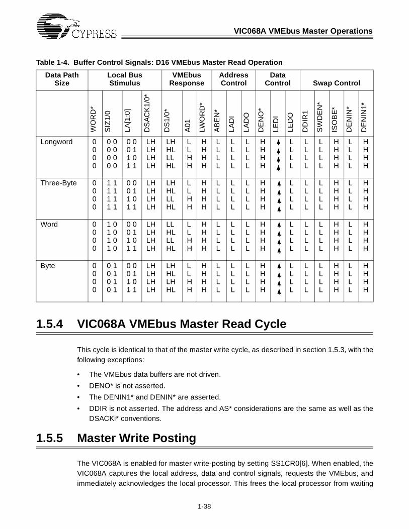
VIC068A VMEbus Master Operations
1-38
1.5.4 VIC068A VMEbus Master Read Cycle
This cycle is identical to that of the master write cycle, as described in section 1.5.3, with thefollowing exceptions:
• The VMEbus data buffers are not driven.
• DENO* is not asserted.
• The DENIN1* and DENIN* are asserted.
• DDIR is not asserted. The address and AS* considerations are the same as well as theDSACKi* conventions.
1.5.5 Master Write Posting
The VIC068A is enabled for master write-posting by setting SS1CR0[6]. When enabled, theVIC068A captures the local address, data and control signals, requests the VMEbus, andimmediately acknowledges the local processor. This frees the local processor from waiting
Table 1-4. Buffer Control Signals: D16 VMEbus Master Read Operation
Data Path Size
Local Bus Stimulus
VMEbus Response
Address Control
Data Control Swap Control
WO
RD
*
SIZ
1/0
LA
[1:0
]
DS
AC
K1/
0*
DS
1/0
*
A01
LWO
RD
*
AB
EN
*
LA
DI
LA
DO
DE
NO
*
LE
DI
LE
DO
DD
IR1
SW
DE
N*
ISO
BE
*
DE
NIN
*
DE
NIN
1*
Longword 0000
0 00 00 00 0
0 00 11 01 1
LHLHLHLH
LHHLLLHL
LLHH
HHHH
LLLL
LLLL
LLLL
HHHH
LLLL
LLLL
LLLL
HHHH
LLLL
HHHH
Three-Byte 0000
1 11 11 11 1
0 00 11 01 1
LHLHLHLH
LHHLLLHL
LLHH
HHHH
LLLL
LLLL
LLLL
HHHH
LLLL
LLLL
LLLL
HHHH
LLLL
HHHH
Word 0000
1 01 01 01 0
0 00 11 01 1
LHLHLHLH
LLHLLLHL
LLHH
HHHH
LLLL
LLLL
LLLL
HHHH
LLLL
LLLL
LLLL
HHHH
LLLL
HHHH
Byte 0000
0 10 10 10 1
0 00 11 01 1
LHLHLHLH
LHHLLHHL
LLHH
HHHH
LLLL
LLLL
LLLL
HHHH
LLLL
LLLL
LLLL
HHHH
LLLL
HHHH

VIC068A VMEbus Master Operations
1-39
for VMEbus arbitration. When VMEbus mastership is obtained, the VIC068A performs thetransfer according to normal VMEbus protocol. Further write-posts are disabled until aDTACK* or BERR* is asserted by the slave. If a BERR* is signaled, the VIC068A can beconfigured to issue a local interrupt by clearing EGICR[6].
If a slave read occurs after a write has been posted but not yet transferred, the latched writedata is “toggled” to the B-to-A latch of the ’543s by asserting the LEDI signal. The slave readthen occurs normally without the write data being written over by the slave read data. Afterthe VIC068A asserts DTACK*, the DENIN1* and DENIN* signals are asserted to drive thewrite data to the A-to-B latch of the ’543. Then LEDO is asserted to again latch the data forthe write operation. This toggling of data is referred to as a Master Write-Post Data Switchback.
1.5.6 Indivisible Cycles
Indivisible cycles can be divided into two categories:
• Indivisible Single-Address Cycles (ISACs)
• Indivisible Multiple-Address Cycles (IMACs)
The VIC068A supports both ISACs and IMACs through many different protocols. Indivisiblecycles can be configured as follows:
1. Request the VMEbus on the assertion of RMC* independent of MWB* (this prevents anyslave access from interrupting local indivisible cycles).
2. Stretch the VMEbus AS*.
3. Make the above behaviors dependent on the local SIZi signals.
These modes are summarized in Table 1-5.
Table 1-5. RMC* Control Map
ICR[7:5] First OperationVMEbus Requested on
RMC* Assertion AS* StretchedVMEbus Held During
RMC* Assertion
X 0 0 Any No No No0 0 1 Any Yes No Yes0 1 0 Any No Yes Yes0 1 1 Any Yes Yes Yes1 0 1 Byte No No No1 0 1 Non-byte Yes No Yes1 1 0 Byte No Yes Yes1 1 0 Non-byte No No No1 1 1 Byte No Yes Yes1 1 1 Non-byte Yes No Yes

VIC068A VMEbus Master Operations
1-40
Address strobe stretching is performed for ISACs in accordance with the VMEbus RMCspecification. For IMACs, the address strobe is typically not stretched in order for slave mod-ules to latch each address.
In the 68K family of processors, ISACs and IMACs are distinguished by the fact that the firstread of an IMAC is never of byte size. This allows for AS* stretching for all RMCs, no RMCs,or only RMCs in which the first transfer was of byte size.
If a processor is not capable of generating indivisible cycles or does not distinguish ISACsfrom IMACs, cycle indivisibility may be guaranteed by using the BCAP release mode outlinedbelow:
1. Set the VIC068A to a BCAP release mode by setting RCR[7:6].
2. Wait for VMEbus grant (BGiIN*).
3. Perform indivisible cycles.
4. Release the VIC068A from BCAP mode in the RCR.
When the VIC068A is the VMEbus slave to a ISAC, the VIC068A maintains the local bus bykeeping LBR* asserted as long as AS* is asserted.
1.5.6.1 Indivisible Single-Address Cycles (ISACs)
The most common implementation of ISACs are of the read-modify-write (RMC) category.This is the only ISAC supported by the VMEbus. The Motorola TAS (Test And Set) instructionis an example of a read-modify-write cycle. The VMEbus specification requires that, for RMCcycles, the VMEbus address strobe be held asserted between the read and the write cycles.Motorola processors prior to the 68020 performed ISACs in the same manner by assertingtheir address strobes for the duration of the cycle. The Motorola processors such as the68020/30/40 provide a signal (RMC* for the 68020/30, and LOCK* for the 68040) to indicatethat a RMC is being performed. The VIC068A has an RMC* signal that is typically connectedto these signals to control ISACs. For RMC cycles, the AS* should be programmed to bestretched.
1.5.6.2 Indivisible Multiple-Address Cycles (IMACs)
The Motorola CAS and CAS2 instructions are examples of IMACs. The VIC068A allows forthe support of IMACs without using the BCAP protocol given in section 1.5.6. In this case,the RMC* signal should be set to request and hold the VMEbus. The local cycle is not allowedto complete until the VMEbus has been obtained. In addition, AS* stretching should be dis-abled so that address latching may be performed by the slave.

VIC068A VMEbus Master Operations
1-41
1.5.7 Deadlock
If the VMEbus is requested in response to MWB* or FCIACK* being asserted, and at thesame time a valid slave select has been signaled, a deadlock has occurred. The VIC068Amay be programmed in the ICR to signal a deadlock in the following ways:
• assert DEDLK*
• assert DEDLK*, LBERR*, and HALT*
• assert DEDLK* and LBERR* (without HALT*) for RMC deadlocks
The first option is typically used for non-Motorola processors without a retry capability. In thatcase, DEDLK* should be used to signal the processor to vacate the local bus (deassertMWB*).
For Motorola 68K applications, the second option may be used to signal the processor toretry the current bus cycle using the Motorola BERR*/HALT* retry mechanism.
For Motorola 68K processors, the HALT*/BERR* retry mechanism is disabled for RMC cycles.In this condition, the third option should be used to signal a generic BERR* to the processor.The BERR* exception processing routines should include software code that checks theSpecial Status Word (SSW) of the 68K BERR* exception stack frames to indicate RMC status.
In all of the above cases, DEDLK* is not deasserted until the slave access causing thedeadlock is compete.
When a cycle is DEDLKed, the VMEbus is still requested. If the VMEbus is granted (after theslave access is complete) and is still available when MWB* is reasserted, the cycle proceedsas normal. If the VMEbus is granted and MWB* is not reasserted, the VIC068A asserts BBSY*for the 90 ns required by the VMEbus specification if it is configured as RWD. If configuredfor ROR, the VIC068A maintains the BBSY* until requested to release it.
1.5.7.1 Undetectable Deadlocks
Poor system design can lead to deadlocks that the VIC068A cannot detect and from whichit cannot recover. Consider the following example:
1. Two boards, CPUa and CPUb, contain a local processor that has dual-ported memoryconnected to both the VMEbus and a VSBbus.
2. CPUa is local bus master and VSBbus master and desires data from CPUb’s memoryover the VSBbus.
3. CPUb is local bus master and VMEbus master and desires data from CPUa’s memoryover the VMEbus.
4. Because both CPUs are their own local bus masters, neither will be able gain access tothe others local bus. DEADLOCK!
VIC068A VMEbus Master Operations
1-42
The VIC068A is not able to detect this deadlock because the VIC068A is only able to monitorthe status of the local bus and the VMEbus. Deadlocks due to the existence of other buses,such as VSB, will not be detected.
The only way to recover from these types of deadlocks is to use bus timeout timers.
1.5.8 Self-Access
If a slave select is signaled while it is the VMEbus master, a self-access has occurred. TheVIC068A signals a self-access by asserting both the LBERR* and BERR* signals. The BESRalso indicates self-access status.
Self-accesses may be used to determine the slave address map of a module.
1.5.9 VMEbus/Local Bus Data and Port Size
A distinction should be made regarding the terms transfer size and port size. Transfer sizeindicates the size of the data in terms of bytes, words, and longwords. The port size indicatesthe physical size of the bus the data will be transferred on. Port sizes for the VMEbus areusually given in terms of D8, D16, and D32 for 8-bit, 16-bit, and 32-bit-wide buses respectively.
The transfer size of the master operation is indicated to the VIC068A by the SIZ1/0 signalsaccording to the following table:
SIZ1 SIZ0 Data Size
0 0 Longword (32 bits) 0 1 Byte (8 bits) 1 0 Word (16 bits) 1 1 3-byte
This information insures proper VMEbus protocol in terms of LWORD*, A01, and DS1/0*. Inaddition, the VIC068A buffer control signals will be properly asserted for the size of the transfer.
The port size of the transfer is indicated by the WORD* signal. When asserted, the mastertransfer is treated as a D16 transfer. For D16 operations, the LWORD* signal is not asserted,and the DS1/0* signals behave appropriately. In addition, the SWDEN* and ISOBE* signalmay be asserted differently in that the D16 VMEbus data located on D[15:0] may be swappedonto the LD[31:16]. This depends on the size of the transfer, the alignment of the transfer,and whether performing a read or a write. Refer to Tables 1-3 to 1-6 for more details on thesesignals for particular cases.
The WORD* signal may be changed dynamically to enable the VIC068A to deal with bothD16 and D32 slaves.
When performing D16 operations, the VIC068A asserts only the DSACK1* signal to indicateto the processor the port size is 16 bits. This would indicate to a 68K processor that when

VIC068A VMEbus Master Operations
1-43
transferring a longword of data, two transfers are required. This is consistent with the Motorola68K DSACKi* dynamic bus-sizing convention.
When using a 16-bit local processor, the WORD* signal must be asserted for all mastertransfers, or strapped Low at power-up to perform D16 transfers. The VIC068A does notsupport using a 16-bit local bus to a 32-bit VMEbus (D32).
1.5.10 Fair Request Timeout
A fair request timeout scheme may be used to prevent VMEbus starvation of any master ina bus request daisy-chain. When operating in a fair request mode, the VIC068A does notassert its BRi* signal until or unless that request level is in its deasserted state. If all boardsin a system obey this fairness doctrine, VMEbus starvation will not occur.
To minimize starvation caused by unfair masters, the VIC068A is also equipped with a fairrequest timeout timer. If the VIC068A is unable to obtain VMEbus mastership within a pro-grammed delay, the VIC068A stops using the fairness doctrine and asserts its BRi* withoutdelay.
Fairness is controlled by writing the ARCR. Fairness is disabled by clearing bits ARCR[3:0].Fairness is enabled (with no timeout) by setting bits ARCR[3:0]. The timeout timer is enabledby writing any other combination to these bits. The value of the timeout is 2 µs times thenumber written. A difference of 2 µs may exist between the value written and the actual delayobserved.
1.5.11 Address-Only Cycles
The VIC068A will not perform address-only cycles. The VIC068A, as slave, can accept ad-dress-only cycles.
1.5.12 The Address Modifiers for Master Cycles
When the VIC068A performs master cycles, it examines the ASIZ1/0 and FC2/1 signals todetermine the value of the AM[5:0] signals that will be driven. The information that the AMcodes specify indicates address sizing and supervisory/user and program/data information.Under normal circumstances, the VIC068A outputs standard VMEbus AM codes. TheVIC068A may also be configured to output user-defined AM codes. This is done with theASIZ1/0 signals and the AMSR. If the ASIZ1/0 signals are both Low, the VIC068A uses theAMSR to determine the value of the AM codes.
If AMSR[7] is clear, VIC068A issues the contents of AMSR[5:0] to the AM[5:0] signals. IfAMSR[7] is set, the VIC068A issues AM codes based on AMSR[5:3] and the FC2/1 inputs.
Table 1-6 summarizes the AM codes for various VIC068A operations and configurations.

VIC068A VMEbus Master Operations
1-44
Table 1-6. Master Transfer AM Code Control Map
VIC068A Master Access Inputs VIC068A AM Code Output
ASIZ1/0 Address Size Block Transfer FC2/1 Operation Type AM[5:0]
0 1 A32 Addressing No 0 00 11 01 1
User DataUser ProgramSupervisory DataSupervisory Program
$09$0A$0D$0E
0 1 A32 Addressing Yes 0 X1 X
User BlockSupervisory Block
$0B$0F
1 1 A24 Addressing No 0 00 11 01 1
User DataUser ProgramSupervisory DataSupervisory Program
$39$3A$3D$3E
1 1 A24 Addressing Yes 0 X1 X
User BlockSupervisory Block
$3B$3F
1 0 A16 Addressing No 0 X1 X
User AccessSupervisory Access
$29$2D
0 0 User DefinedAMSR[7] = 0
Yes/No User Defined AMSR[5:0]
0 0 User DefinedAMSR[7] = 1
Yes/No
0 00 11 01 1
User Defined AMSR[5:3]+$01$02$05$06

1-45
1.6VIC068A VMEbus Slave
OperationsThe act of writing or retrieving data for a VMEbus master is referred to as a slave operation.The VIC068A is able to perform slave operations with extensive configuration options.
The following VIC068A registers are used in performing and configuring slave operations:
• Slave Select 0 Control Register 0 (SS0CR0), bits 0–5
• Slave Select 0 Control Register 1 (SS0CR1)
• Slave Select 1 Control Register 0 (SS0CR0), bits 0–5
• Slave Select 1 Control Register 1 (SS0CR1)
• Local Bus Timing Register (LBTR)
• Address Modifier Source Register (AMSR)
1.6.1 The Valid Slave Select
The VIC068A contains two separate signals that are used to indicate that the VIC068A hasbeen selected for a slave access. These signals are SLSEL0* and SLSEL1*. These signalsare usually the result of external VMEbus address decoding. When the VIC068A detects aSLSELi* asserted, the VIC068A waits for:
• AS* asserted
• DSi* asserted for the current cycle (not left over from previous cycle)
• DTACK* or BERR* deasserted from previous cycle
The VIC068A then checks the AM codes for:
• address sizing (A32/A24/A16)
• transfer type (supervisory/user)
If the VIC068A is configured, in SSiCR0, to accept the slave access as indicated by the AMcodes, the VIC068A proceeds with the slave request by asserting the LBR* signal to obtainthe local bus. If the VIC068A is not configured for the particular type of slave access, theVIC068A ignores the request and does not assert LBR*.
If the VIC068A has been selected for valid D32 slave access and the VIC068A is configuredto accept only D16 operations, the VIC068A asserts BERR*. If the WORD* signal is asserted,the VIC068A will only accept D16 slave cycles, independent of how the VIC068A may beconfigured in the SSiCR0. If the VIC068A is not configured to accept block transfers, anyblock transfer request will be BERRed.

VIC068A VMEbus Slave Operations
1-46
The VIC068A is also capable of bypassing the standard VMEbus AM codes and qualifyingthe SLSELi* with user-defined AM codes. If enabled for this operation (in SSiCR0[3:2]), theVIC068A compares the AM codes with the value contained in the AMSR[5:0]. If the valuesmatch, a valid slave select has occurred. The VIC068A may also be configured to only com-pare AM[5:3] to AMSR[5:3]. When enabled for this operation by setting AMSR[6], the addresssize is also qualified by the address size information in the SSiCR0. Table 1-7 summarizesthe AM code operations for VIC068A slave accesses.
In some situations, it is possible for both SLSEL1* and SLSEL0* to be asserted simultaneous-ly. In this case, the VIC068A checks each SLSELi*’s register configuration with the AM codesto determine which, if any, valid slave select has occurred.
Also included in the AM codes is information specifying if the transfer is a block transfer. TheVIC068A checks the SSiCR0 register to determine if the VIC068A is enabled to receive slaveblock transfers. Slave block transfers are discussed in detail in section 1.10.2.
1.6.2 The Local Bus Request
After a valid slave select has been signaled, the VIC068A bids for the local bus by assertingthe LBR* signal. This signal should be input to a local bus arbiter, which in turn issues a busgrant (assert LBG*) to the VIC068A. The VIC068A does not perform local bus arbitration.
Table 1-7. Slave Transfer AM Code Control Map
VIC068A AM Code Inputs VIC068A Slave Access Outputs
Operation Type AM[5:0] Address Size Block Transfer FC2/1
User DataUser ProgramSupervisory DataSupervisory Program
$09$0A$0D$0E
A32 Addressing No 1 0
User BlockSupervisory Block
$0B$0F
A32 Addressing Yes 0 0
User DataUser ProgramSupervisory DataSupervisory Program
$39$3A$3D$3E
A24 Addressing No 1 0
User BlockSupervisory Block
$3B$3F
A24 Addressing Yes 0 0
User AccessSupervisory Access
$29$2D
A16 Addressing No 1 0
User Defined User Defined User Defined No 1 0
User Defined User Defined User Defined Yes 0 0

VIC068A VMEbus Slave Operations
1-47
1.6.3 The Local Bus Grant
Once the VIC068A issues the LBR*, the VIC068A waits for the assertion of the local busgrant. If the local processor expects BGACK-type signaling in response to the assertion ofBG*, this must be generated by external logic. This BGACK must continue to be asserteduntil LBR* is deasserted.
After the assertion of LBG*, the VIC068A waits for 3T+tPD before enabling the local address
drivers (and data drivers if writing). At this point, the VIC068A waits 1T+tPD before driving
PAS*. If local resources cannot be guaranteed to be off the local bus by these times after theassertion of LBG*, additional delay may need to be introduced between the assertion of abus grant from the local arbiter and the assertion of LBG* to the VIC068A. See Figure 1-30in Chapter 1.13 for more details on local bus timing.
When the VIC068A begins driving the local bus, it also drives the FC2/1 signals with infor-mation on the type of local cycle it is performing. These function codes should not be confusedwith the function codes that are driven to the VIC068A when it is performing VMEbus mastercycles (see section 1.5.12). The function code outputs for the VIC068A are as follows:
FC2 FC1 Description
0 0 Slave Block Transfer 0 1 Block Transfer with Local DMA1 0 Standard Slave Access 1 1 DRAM Refresh
1.6.4 Local Bus Timing
The VIC068A contains a Local Bus Timing Register (LBTR) for configuring the minimum PAS*assertion and deassertion and DS* deassertion times. For single cycle slave accesses, theminimum deassertion time is not considered in that PAS* and DS* are asserted according tothe timing discussed in section 1.6.3. The minimum deassertion times for PAS* and DS* areusually used when performing multiple back-to-back local cycles such as DRAM refreshcycles, slave block transfers, and master block transfers with local DMA. The minimum as-sertion time for PAS* should be set so that illegal memory access cycles can never occur forthe particular memory devices being used. Minimum PAS* asserted time is usually dictatedby the assertion of the DSACKi* signals, which start an additional delay circuit called the SATdelay (see section 1.6.8). Figures 1-6 and 1-7 show an example of local reads and writes.

VIC068A VMEbus Slave Operations
1-48
Figure 1-6. Local Bus Cycle—Write
Figure 1-7. Local Bus Cycle—Read
OUTPUT
OUTPUT
OUTPUT
OUTPUT
OUTPUT
OUTPUT
OUTPUT
INPUT
INPUT
LA[7:0]SIZ1/0FC2/1
ASIZ1/0WORD*
LAEN
R/W*
PAS*
DS*
LD[7:0]
LBR*
LBG*
DSACK*
OUTPUT
OUTPUT
OUTPUT
OUTPUT
OUTPUT
OUTPUT
OUTPUT
INPUT
INPUT
LA[7:0]SIZ1/0FC2/1
ASIZ1/0WORD*
LAEN
R/W*
PAS*
DS*
LD[7:0]
LBR*
LBG*
DSACK*
VIC068A VMEbus Slave Operations
1-49
1.6.5 VMEbus/Local Bus Data and Port Size
After receiving a valid slave select, the VIC068A examines the DS1/0*, A01, and LWORD*signals to determine the size and the alignment of the transfer. The VIC068A then drives theSIZ1/0 and LA[1:0] signals with the appropriate values. The SIZ1/0 codes are given below:
SIZ1 SIZ0 Transfer Size
0 0 Longword 0 1 Byte 1 0 Word 1 1 3-byte
The ability to handle D32 transfers is configured in the SSiCR0[4]. If configured as a D32port, the VIC068A accepts any size VMEbus transfer. If programmed as a D16 port only, theVIC068A will assert BERR* for all D32 requests. The VIC068A determines D32 and D16 fromthe LWORD* signal.
1.6.6 The Latched Bus Interface
When a slave read is performed, data is read from local memory and latched into the VMEbusdata transceivers. LD[7:0] is latched into the VIC068A and LD[31:8] is latched into externaldevices such as the CY7C964s. After DSACKi* is asserted, the VIC068A begins the SATdelay(SSiCR1[3:0]). After this delay times out, the VIC068A asserts both DTACK* and LEDO.These signals are held until both DS1/0* are deasserted.
During a slave write access, the VIC068A asserts the LEDI signal immediately after receivinga valid slave select latching the data into the data transceivers.
1.6.7 Slave Write Posting
The VIC068A is able to perform slave write posting, when SS1CR0[7] is set. In this mode,the VIC068A, after receiving a valid slave select, latches the incoming data (asserts LEDI)and immediately asserts DTACK*. The VIC068A requests the local bus and then performsthe local write cycle independent of VMEbus activity.
If a slave write post is requested while a previous slave write post is currently being serviced,DTACK* is not asserted until the local write is complete. At this point, the VIC068A posts thewrite normally. Slave write posts should be used with caution. If there was a problem with thelocal portion of the cycle (i.e., LBERR* was asserted), the initiator of the cycle may neverknow that the cycle did not complete since DTACK* was already asserted.

VIC068A VMEbus Slave Operations
1-50
1.6.8 Slave Acknowledge Timing (SAT)
Once DSACKi* is asserted, the delay defined by SSiCR1[3:0] begins. After this delay expires,DTACK* is asserted, and PAS* and DS* deassert. LEDO is also asserted if the slave cycleis a read. An assertion of any or both of the DSACKi* signals is considered an acknowledgeand begins this timeout. The default value for these delays is 0. Usually delays need only beused for memory designs that use an advance acknowledge or late bus-error algorithms.Once DTACK* is asserted, the VIC068A maintains DTACK* until the VMEbus DSi* signalsare deasserted.
If the LBERR* signal is asserted, the VIC068A asserts BERR* until the DSi* signals aredeasserted. If LBERR* is asserted after either DSACKi* has been asserted, and the DSACK*-to-DTACK* delay has not yet expired, DTACK* is inhibited and the BERR* signal will beasserted on the VMEbus without delay. If the user employs some delayed LBERR* algorithm(such as late parity check), the SAT delay must be programmed sufficiently long to allow forthis delay of LBERR*.
Table 1-8. Buffer Control Signals: D32 VMEbus Slave Write Operation
Data PathSize
VMEbusStimulus
Local BusResponse
AddressControl
DataControl Swap Control
WO
RD
*
SIZ
1/0
LA
[1:0
]
DS
AC
K1/
0*
DS
1/0
*
A01
LWO
RD
*
AB
EN
*
LA
DI
LA
DO
DE
NO
*
LE
DI
LE
DO
DD
IR1
SW
DE
N*
ISO
BE
*
DE
NIN
*
D32D32, UAT (0-2)D32, UAT (1-3)D32, UAT (1-2)
0 00 11 00 0
0001
0000
LLHHHHHL
LLLLLHLH
0000
HHHH
LLLL
HHHH
LLLL
LLLL
HHHH
LLLL
LLLL
LLLL
D16 (0-1)D16 (2-3)
0 00 0
01
11
HLHL
LLHL
00
HH
LL
HH
LL
LL
LL
LL
LL
HH
D8 (0)D8 (1)D8 (2)D8 (3)
0 11 00 11 0
0011
1111
LHLHLHLH
LLLHHLHH
0000
HHHH
LLLL
HHHH
LLLL
LLLL
LLLL
LLLL
LLLL
HHHH

VIC068A VMEbus Slave Operations
1-51
.
Table 1-9. Buffer Control Signals: D32 VMEbus Slave Read Operation
Data PathSize
VMEbusStimulus
Local BusResponse
AddressControl
DataControl Swap Control
WO
RD
*
SIZ
1/0
LA[1
:0]
DS
AC
K1/
0*
DS
1/0
*
A0
1
LWO
RD
*
AB
EN
*
LAD
I
LAD
O
DE
NO
*
LED
I
LED
O
DD
IR1
SW
DE
N*
ISO
BE
*
DE
NIN
*
D32D32, UAT (0-2)D32, UAT (1-3)D32, UAT (1-2)
0 00 11 00 0
0001
0000
LLHHHHHL
LLLLLHLH
0000
HHHH
LLLL
LLLL
LLLL
HHHH
HHHH
LLLL
HHHH
HHHH
D16 (0-1)D16 (2-3)
0 00 0
01
11
HLHL
LLHL
00
HH
LL
LL
LL
HH
LH
HL
HH
HH
D8 (0)D8 (1)D8 (2)D8 (3)
0 11 00 11 0
0011
1111
LHLHLHLH
LLLHHLHH
0000
HHHH
LLLL
LLLL
LLLL
HHHH
LLHH
HHLL
HHHH
HHHH
Table 1-10. Buffer Control Signals: D16 VMEbus Slave Read Operation
Data PathSize
VMEbusStimulus
Local BusResponse
AddressControl
DataControl Swap Control
WO
RD
*
SIZ
1/0
LA
[1:0
]
DS
AC
K1/
0*
DS
1/0
*
A01
LWO
RD
*
AB
EN
*
LA
DI
LA
DO
DE
NO
*
LE
DI
LE
DO
DD
IR1
SW
DE
N*
ISO
BE
*
DE
NIN
*
D16 (0-1)D16 (2-3)
0 00 0
01
11
HLHL
LLHL
00
HH
LL
LL
LL
HH
LH
HL
HH
HH
D8 (0)D8 (1)D8 (2)D8 (3)
0 11 00 11 0
0011
1111
LHLHLHLH
LLLHHLHH
0000
HHHH
LLLL
LLLL
LLLL
HHHH
LLHH
HHLL
HHHH
HHHH

VIC068A VMEbus Slave Operations
1-52
Table 1-11. Buffer Control Signals: D16 VMEbus Slave Write Operation
Data PathSize
VMEbusStimulus
Local BusResponse
AddressControl
DataControl Swap Control
WO
RD
*
SIZ
1/0
LA[1
:0]
DS
AC
K1/
0*
DS
1/0
*
A0
1
LWO
RD
*
AB
EN
*
LAD
I
LAD
O
DE
NO
*
LED
I
LED
O
DD
IR1
SW
DE
N*
ISO
BE
*
DE
NIN
*
D16 (0-1)D16 (2-3)
0 00 0
01
11
HLHL
LLHL
00
HH
LL
HH
LL
LL
LL
LL
LL
HH
D8 (0)D8 (1)D8 (2)D8 (3)
0 11 00 11 0
0011
1111
LHLHLHLH
LLLHHLHH
0000
HHHH
LLLL
HHHH
LLLL
LLLL
LLLL
LLLL
LLLL
HHHH

1-53
1.7VIC068A Control Register
Access1.7.1 Control Registers
The VIC068A contains 58 8-bit internal registers addressable from the local bus. Theseregisters provide complete control and monitoring of the VIC068A.
1.7.2 Control Register Access
Access to internal registers of the VIC068A is accomplished through the assertion of CS*,PAS* and DS*. It is the value of R/W* that determines if the access is a read or a write.
When CS*, PAS* and DS* are all driven Low (in any order) to the VIC068A, access to aninternal register is initiated (i.e., REGISTER_ACCESS* = 0 when (CS*[0] and PAS*[0]and DS*[0]). Register access completes when either CS*, PAS*, or DS* deassert (i.e.,REGISTER_ACCESS* = 1 when (CS*[1] or PAS*[1] or DS*[1]). Figure 1-8 shows a timingdiagram of the VIC068A internal register accesses. The timing values are explained in Table1-12.
Although the registers are 8 bits wide, the VIC068A always acknowledges a registeraccess with both DSACK*s. This is because the VIC068A registers are addressed onlongword boundaries and occupy 32 bits of address space.
Table 1-12. Register Access Timing Values
OperationCommercial Industrial Military
Min. Max. Min. Max. Min. Max.REGISTER ACCESSM1 PAS*[0] & DS*[0] & CS*[0] to
DSACKi*[L]4T+5 5T+34 4T+5 5T+35 4T+4 5T+38
M2 PAS*[0] & DS*[0] & CS*[0] to LD[7:0] Valid
3T+5 4T+28 3T+5 4T+29 3T+4 4T+37
M3 AS*[0] & ICFSEL*[0] to DTACK*[L]
4T+6 4T+30 4T+5 4T+31 4T+5 4T+34
M4 PAS*[0] & DS*[0] & CS*[0] to LD[7:0], LA[7:0] Valid
2T+6 3T+30 2T+5 3T+31 2T+5 3T+34

VIC068A Control Register Access
1-54
Figure 1-8. VIC068A Internal Register Access Timing
When reading a register, the VIC068A delivers data on LD[7:0]. When writing data, theVIC068A must see data on LD[7:0]. Because of this, the VIC068A only acknowledges aregister access that is addressed “correctly” according to the following table:
PAS*
DS* INPUT
INPUT
INPUT
INPUT
OUTPUT
INPUT
CS*
R/W*
DSACK1/0*
LD[7:0]
Write
M1
ReadPAS*
DS* INPUT
INPUT
INPUT
INPUT
OUTPUT
OUTPUT
CS*
R/W*
DSACK1/0*
LD[7:0]
M1
M2
INTERNALREGISTERACCESS*
INPUTLA[7:0]
valid
valid
M4
INPUTLA[7:0] valid
M4
INTERNALREGISTERACCESS*
valid

VIC068A Control Register Access
1-55
SIZ1, SIZ0 VIC068A acknowledges if LA[1:0] is:
0 0 0 00 1 1 11 0 1 01 1 1 1
This insures that data will be available to/from LD[7:0] according to 68K protocol.
The VIC068A addresses given in this user’s guide are byte addresses located at theLA[1:0] = 1 1 position. This implies that if the registers are to be addressed through alongword access, LA[1:0] must be 0 0. If accessed though a word access, LA[1:0] mustbe 1 0.
For example, if the variable vic contains the VIC068A register base address for a particularapplication, the following Motorola instructions would identically move the DMASR data(address = $BF) to the Motorola D0 register:
move.b (vic,$bf), d0
move.w (vic,$be), d0
move.l (vic,$bc), d0
1-56
1.8Interprocessor
Communication FacilitiesThe VIC068A contains three categories of interprocessor communication facilities (ICFs):
• Interprocessor Communication Registers (ICRs)
• Interprocessor Communication Global Switches (ICGSs)
• Interprocessor Communication Module Switches (ICMSs)
The ICRs are 8-bit registers that may be accessed from either the local bus or the VMEbus.
The ICGSs and the ICMSs are switches that may be set to interrupt the local processor.
These facilities are located in seven registers that are visible from both the local bus andthe VMEbus. When accessed via the local bus, the registers are read/written by normalVIC068A register access methods. When accessed via the VMEbus, the ICFSEL* signalis used as a register select signal. The register addresses, when accessed from the localbus are not the same as when accessed from the VMEbus. The VIC068A contains aninternal arbiter to arbitrate between local and VMEbus accesses to these facilities.
Additional registers used for the ICFs are as follows:
• ICGS Interrupt Control Register (ICGSICR)
• ICMS Interrupt Control Register (ICMSICR)
• ICGS Interrupt Vector Base Register (ICGSIVBR)
• ICMS Interrupt Vector Base Register (ICMSIVBR)
• Interprocessor Communication Switch Register (ICSR)
1.8.1 Valid ICF Selection
The ICFSEL* signal is used to signal that the VMEbus master desires access to theVIC068A interprocessor communication facilities. This signal is usually driven from VME-bus address decoders. When ICFSEL* is asserted, the VIC068A checks A[5:1] to deter-mine what ICF is desired. Self-access to the ICF facilities is not detected by the VIC068A.The VIC068A then verifies the AM codes against the following table:

Interprocessor Communication Facilities
1-57
ICF AM code(s)
ICR $29, $2D (A16, user or supervisory data)
ICGS $2D (A16, supervisory data)
ICMS $29, $2D (A16, user or supervisory data)
Once a valid ICF select has occurred, the VIC068A then processes the request. The ICFVMEbus address is shown in Table 1-13.
1.8.2 Interprocessor Communication Registers
The VIC068A contains seven interprocessor communication registers (ICRs). These reg-isters are accessible from both the local bus and the VMEbus. ICRs 4–0 are consideredgeneral-purpose read/write registers. ICR5 is the VIC068A version/revision register. Thevalue of this register indicates the mask revision of the device. ICR6 contains HALT* andRESET* status of the VIC068A. ICR7 provides semaphores for ICRs 5–0. These sema-
Table 1-13. ICF VMEbus Address Map
A7 A6 A5 A4 A3 A2 A1 LWORD Function
XXXXXXXX
XXXXXXXX
00000000
00000000
00001111
00110011
01010101
11111111
ICR0 Access ICR1 Access ICR2 Access ICR3 Access ICR4 Access ICR5 Access ICR6 Access ICR7 Access
XXXXXXXX
XXXXXXXX
00000000
11111111
00000000
00001111
00110011
01010101
Clear ICGS0 Set ICGS0 Clear ICGS1 Set ICGS1 Clear ICGS2 Set ICGS2 Clear ICGS3 Set ICGS3
XXXXXXXX
XXXXXXXX
11111111
00000000
00000000
00001111
00110011
01010101
Clear ICMS0 Set ICMS0 Clear ICMS1 Set ICMS1 Clear ICMS2 Set ICMS2 Clear ICMS3 Set ICMS3
X X 1 1 X X X X Undefined/Reserved
Interprocessor Communication Facilities
1-58
phores are set whenever ICRs 5–0 are written. In addition, ICR7 also indicates VMEbusmastership and a mask for SYSFAIL*. Refer to Chapter 1.12 for detailed register descriptions.
1.8.3 Interprocessor Communication Global Switches
The ICGSs are software switches that may be set over the VMEbus to interrupt a groupof VMEbus modules.
When the VIC068A issues the global switches, it is performing a VMEbus byte-wide writeto the pre-defined global switch address.
If the global switch interrupts are enabled in the ICGSICR of the VIC068A slave, a localinterrupt is generated on a clear-to-set transition of the selected switch. When acknowl-edged (FCIACK* asserted), the slave VIC068A handles the interrupt by returning thestatus/ID value from the ICGSVBR. See Chapter 1.9 for details on VIC068A interrupt gener-ation and handling. Once a switch is set, it must be cleared before it can be re-set.
Because the global switches are meant to be issued to several modules, the VIC068A asVMEbus master must assert DTACK* to complete the VMEbus cycle. The VIC068A issuesDTACK* if the ICFSEL* signal is asserted while performing the VMEbus master cycle.
Notice that if a valid ICF select has occurred, A[2:1] selects the ICGS switch and A0 (i.e.,DS1* and DS0*) indicates whether the switch is to be set or cleared. That is, a byte-widewrite to an even address clears the selected switch and a byte-wide write to an odd addresssets the selected switch.
The ICSR may be used to provide monitoring of the global switches.
1.8.4 Interprocessor Communication Module Switches
Like the ICGSs, the ICMSs are software switches that may be set over the VMEbus tointerrupt the local processor. The module switches, however, are meant to be issued to aspecific module.
As in the global switches, the VIC068A issuing the module switches performs a VMEbusbyte-wide write to the pre-defined switch address.
Because the module switches are meant for a specific module, the VIC068A as VMEbusslave (the module whose switch was just set) must assert the DTACK*. The VIC068Aissuing the ICMS need not have its ICFSEL* signal asserted.
The interrupt and addressing mechanisms are the same for ICMSs as they were for ICGSs.
The ICSR may be used to provide monitoring of the module switches. Unlike the globalswitches, this register may be written by local resources to interrupt the CPU.

1-59
1.9Interrupts
The VIC068A offers complete VMEbus and local bus interrupt generation and handlingfunctions. In addition, the VIC068A also offers error and status interrupts for variousVIC068A features. Local interrupt 2 (LIRQ2) may also be used as a periodic “heartbeat”timer. Significant control over the VIC068A interrupt generation/handling capabilitiesthrough the control registers listed below (32 of the 59 VIC068A control registers are forinterrupt generation/handling):
• VMEbus Interrupter Interrupt Control Register (VIICR)
• VMEbus Interrupt Control Registers 1–7 (VICR1–7)
• DMA Status Interrupt Control Register (DMASICR)
• Local Interrupt Control Registers 1–7 (LICR1–7)
• ICGS Interrupt Control Register (ICGSICR)
• ICMS Interrupt Control Register (ICMSICR)
• Error Group Interrupt Control Register (EGICR)
• ICGS Interrupt Vector Base Register (ICGSIVBR)
• ICMS Interrupt Vector Base Register (ICMSIVBR)
• Local Interrupt Vector Base Register (LIVBR)
• Error Group Interrupt Vector Base Register (EGIVBR)
• VMEbus Interrupt Request/Status Register (VIRSR)
• VMEbus Interrupt Vector Base Registers 1–7 (VIVBR1–7)
1.9.1 VMEbus Interrupter
The VIRSR controls the assertion of the VMEbus interrupts. VIRSR[7:1] control the as-sertion (and deassertion if desired) of IRQ*7–1 signals respectively. VIRSR[0] enablesthe setting and clearing of these bits. To issue an interrupt, both the interrupt bit andVIRSR[0] must be set. To clear an interrupt, the interrupt bit must be set and VIRSR[0]must be cleared. VIRSR[7:1] may also be read to indicate the status of pending VMEbusinterrupts. For example, if vic contains the base address of the VIC068A registers, thefollowing 68K code could be used to assert IRQ4*:
move.b #$11,(vic,$83)
This code would clear the interrupt:
move.b #$10,(vic,$83)
Interrupts
1-60
Once the interrupt is issued, the handler for that interrupt proceeds with the interruptacknowledge cycle. Once the VIC068A recognizes a valid interrupt acknowledge cycle(IACKIN* asserted), it places the status/ID vector, located in the VIVBRi, on the D[7:0]lines. The VIC068A is capable of issuing 8-bit status/IDs only. The VIC068A uses a Re-lease-On-AcKnowledge (ROAK) for the normal deassertion of the IRQi* signals.
More than one VMEbus interrupt may be issued or pending simultaneously by the sameVIC068A interrupter.
1.9.2 The VIC068A VMEbus Interrupt Handler
The VIC068A may be enabled to handle VMEbus interrupts. If VICR1–7[7] is clear, theVIC068A handles all pending interrupts on that respective level. Only one VMEbus moduleshould be configured to handle any given interrupt level per VMEbus system.
The VIC068A performs D8 interrupt acknowledge cycles only.
When the VIC068A detects a pending VMEbus interrupt, it performs the following func-tions:
1. Assert the IPLi signals with the value programmed in the VICRi.
2. Wait for the assertion of the FCIACK* signal, which indicates the local processor isacknowledging a local interrupt.
3. Once FCIACK* is asserted, sample LA[3:1] to determine the IPL value of local interruptbeing acknowledged.
4. If matched, obtain VMEbus mastership, assert IACK*, drive A[3:1]=interrupt-level andenable D[7:0] to the local data bus LD[7:0].
5. Once DTACK* is asserted by the VMEbus interrupter indicating the status/ID byte isvalid on D[7:0], the VIC068A asserts DSACKi* to complete the local interrupt acknowl-edge cycle and indicates that the status/ID is available on LD[7:0].
The LA[3:1] matching described in step 3 is discussed in section 1.9.3.
Table 1-14 summarizes the VMEbus interrupt acknowledge cycle.

Interrupts
1-61
Table 1-14. VMEbus Interrupt Acknowledge Cycle
Step VIC068A Interrupter VIC068A Handler Local Processor
1 Generate IRQi* (write to VIRSR)
2 Detect IRQi* asserted (VICRi enabled to handle interrupt)
3 Assert inverted version of IPLi value as programmed in the VICRi
4 Detect IPLi asserted
5 Place inverted IPL level of interrupt being handled on LA[3:1]
6 Assert FCIACK*, PAS*, DS*
7 Detect FCIACK* asserted
8 Sample LA[3:1] for request level being acknowledged
9 If matched, obtain VMEbus mastership
10 Assert IACK* and place number of IRQ being ac-knowledged on A[3:1]
11 Enable D[7:0] to capture status/ID vector
12 Detect IACKiIN* asserted and sample A[3:1]
13 If A[3:1] matches IRQ number requested, drive status/ID vec-tor programmed in the VIVBRi
14 Assert DTACK*
15 Generate interrupt acknowl-edged interrupt if enabled in the VIICR
Assert DSACKi*
16 Capture status/ID
17 Enter Interrupt Service Routine

Interrupts
1-62
1.9.3 Local Interrupt Handler
The VIC068A may be enabled to handle local interrupts in addition to VMEbus interrupts.Local interrupt handling is enabled through the LICRs 1–7. If bit 7 is cleared in any ofthese registers, the corresponding local interrupt is handled by the VIC068A. The localinterrupts may be configured in a variety of ways including edge or level sensitivity, activeHigh/Low levels, or rising/falling edges. The VIC068A may be configured to supply, orautovector, the status/ID. If VIC068A is configured to supply the status/ID vector, the vectoris supplied from the LIVBR. Unlike the VIVBRs, this is a single register. The upper 5 bitsare user-defined, and the lower 3 bits are dynamic to indicate the interrupt value(LIRQ7*...LIRQ1*, etc.). These lower 3 bits are place-holders only. They may not indicatethe interrupt value if read, even during an interrupt acknowledge cycle. If the VIC068A isconfigured for autovectoring (VIC068A does not supply status/ID), the VIC068A assertsthe LIACKO* signal after the interrupt is acknowledged (FCIACK* asserted) by the localprocessor. This should indicate to the interrupter to place the status/ID on D[7:0] signallines and assert DSACKi*. LIACK0* may be connected to the 68K AVEC signal for internalgeneration of the interrupt vector.
Once the VIC068A detects LIRQi* asserted, and the VIC068A is enabled to handle thatinterrupt, the VIC068A proceeds as follows:
1. Assert the IPLi signals with the value programmed in the LICRi.
2. Wait for the assertion of the FCIACK* signal, which indicates the local processor isacknowledging a local interrupt.
3. Once FCIACK* is asserted, sample LA[3:1] to determine the IPL value of local interruptbeing acknowledged.
• If matched,
— drive LD[7:0] with status/ID if enabled to supply vector and assert DSACKi*.
— or, assert LIACK0* if not enabled to supply vector (autovectoring).
The LA[3:1] matching described in step 3 is required to distinguish an acknowledge fromamong multiple pending interrupts. If the value of LA[3:1] does not match the value of theIPL signals (see section 1.9.8 for positive/negative logic issues regarding the IPL signals),the VIC068A assumes the acknowledge is not for it. The 68K family of processors assertsLA[3:1], as described above, automatically. Table 1-15 summarizes the local interrupt ac-knowledge cycle.

Interrupts
1-63
1.9.4 The FCIACK Cycle
When the VIC068A detects an interrupt (either VME or local) that it has been programmedto handle, the VIC068A begins a FCIACK cycle. The IPL value associated with that inter-rupt (as programmed in VIICR, VICR1–7, DMASICR, LICR1–7, ICGSICR and ICMSICR)is placed into an internal lookup table and driven (inverted) onto the IPL lines. The valueplaced onto LA[3:1] by the local processor during a FCIACK cycle is compared with thelookup table within the VIC068A. If a match is found, the interrupt that the local processorhas agreed to service is handled.
Since interrupts occur asynchronous to each other, it is possible for the value of the IPLlines to change without warning. If the IPL lines were not sampled prior to them changing,that interrupt will not be seen by the local processor until all higher priority interrupts havebeen handled. Once FCIACK* is asserted to the VIC068A, the IPLi lines will be frozenuntil the Interrupt Acknowledge cycle is complete. Since the value placed onto LA[3:1] bythe local processor is compared against a lookup table and not the current value of the
Table 1-15. Local Interrupt Acknowledge Cycle
Step Local Interrupter VIC068A Handler Local Processor
1 Generate LIRQi*
2 Assert inverted version of IPLi val-ue programmed in the LICRi
3 Detect IPLi asserted
4 Place inverted IPL level of interrupt be-ing handled on LA[3:1]
5 Assert FCIACK*, PAS*, DS*
6 Detect FCIACK* asserted
7 Sample LA[3:1] for request level being acknowledged
8a If matched, drive status/ID on LD[7:0] programmed in the LICRi
9a Assert DSACKi*
8b Assert LIACK0*
9b Drive status/ID, DSACKi*
10 Capture status/ID
11 Enter ISR

Interrupts
1-64
IPL lines the VIC068A will handle any pending interrupt that the local processor agreesto handle during a FCIACK cycle.
1.9.5 The Error/Status Interrupts
The VIC068A is capable of generating local interrupts on certain error or status conditions.The error group interrupts include:
• SYSFAIL* assertion. An interrupt is generated when SYSFAIL* is detected by some-thing other than the VIC068A.
• ACFAIL* assertion. An interrupt is generated when ACFAIL* is detected.
• Write post failure. An interrupt is generated when a master write post has failed dueto a LBERR* or BERR* assertion.
• VMEbus arbitration failure. An interrupt is generated if the VIC068A is system controllerand the VMEbus arbitration timeout timer expires.
The IPL value asserted for these error group interrupts is contained in the EGICR. Thereis only one IPL value for the error group interrupts.
The VIC068A contains two status interrupts:
• The DMA complete interrupt. An interrupt is generated when a block transfer with localDMA is complete (successful or unsuccessful). The IPL value issued is also containedin the DMAICSR.
• The Interrupter interrupt acknowledge. An interrupt is generated upon the acknowl-edgment of a previously issued VMEbus interrupt. The IPL value issued is containedin the VMEIICR.
Upon local acknowledgment of both the error and status group interrupts, the VIC068Aissues the status/ID byte located in the EGIVBR. EGIVBR[7:3] are user defined.EGIVBR[2:0] are dynamic to indicate the particular interrupt being acknowledged.
1.9.6 Interrupt Priority Order
The 29 interrupt sources of the VIC068A are grouped into 19 priority categories. Withmultiple interrupts pending, the VIC068A issues the interrupts in the following order:
Priority Interrupt
1 LIRQ7* 2 Error Group 3 LIRQ6* 4 LIRQ5* 5 LIRQ4* 6 LIRQ3*
Interrupts
1-65
7 LIRQ2* 8 LIRQ1* 9 ICMS Group 10 ICGS Group 11 IRQ7* 12 IRQ6* 13 IRQ5* 14 IRQ4* 15 IRQ3* 16 IRQ2* 17 IRQ1* 18 DMA Complete 19 VMEbus Interrupter
Notice that the priority of the interrupts within the VIC068A is not dependent on the IPLvalues programmed in the interrupt control registers. This, combined with the fact thatVMEbus interrupt priority is also governed by the position of the module within a VMEbussystem, makes determining actual interrupt priority for a given processor in a given VME-bus system flexible.
If an interrupt is pending, and another higher-priority interrupt (according to the abovetable) is issued to the VIC068A, the VIC068A will change the state of the IPL lines to thatof the higher-priority interrupt. The VIC068A, however, still handles the lower-priority in-terrupt if it is acknowledged before the higher one. If the lower-priority interrupt is beingacknowledged (FCIACK* asserted) at the time of the assertion of the higher-priority in-terrupt, the IPL signals will not change until the interrupt acknowledge cycle is complete.
While an interrupt is pending, all lower-priority interrupts subsequently issued are queuedwithin the VIC068A and issued at the completion of the pending interrupt’s acknowledgecycle.
1.9.7 Clock-Tick Interrupt Generator
LIRQ2 may be enabled to function as a “heartbeat” interrupt generator issuing periodicinterrupts. If the interrupt generator is enabled by configuring SS0CR0[7,6], the LIRQ2*pin is converted to an output and issues periodic interrupts in 50-, 100-, or 1000-Hzfrequencies. This interrupt should be considered an edge-triggered interrupt since it maybe deasserted before the interrupt is acknowledged. The VIC068A may also be configuredto handle the interrupt by enabling LIRQ2* in LICR2. In this case, the interrupt is consideredto be like any other interrupt issued to the VIC068A and normal interrupt acknowledgeprocedures apply.

Interrupts
1-66
1.9.8 Interrupt Control Registers
The IPL values programmed in the interrupt control registers are positive logic values.This is unlike the value of the IPL signals asserted to the processor by the VIC068A, whichare negative logic. The VIC068A performs this complementing of values internally. Thatis, if a value of 010 (positive logic 2) is programmed into an interrupt control register, thevalue of 101 (negative logic 2) is driven on the IPL signals.
When local resources are acknowledging an interrupt and driving LA[3:1] with the levelof the interrupt being acknowledged, LA[3:1] should contain the positive logic value of theinterrupt.
Mask bits exist for every interrupt the VIC068A is capable of generating. These mask bitsare set (interrupts disabled) after a global reset. When changing the level and/or polaritiesof the local interrupts, it is recommended that the interrupts be masked prior to this andre-enabled after.

1-67
1.10VIC068A Block Transfer
FunctionsThe ability to transfer large blocks of data at a high-sustained transfer rate is paramountin today’s VMEbus market. When implemented properly, transfer rates exceeding 30Mbyte/sec can be obtained using a high-speed processor, high-speed memory and high-speed VMEbus interfaces such as the VIC068A.
1.10.1 VIC068A Master Block Transfer
The VIC068A can be configured for block transfers while the local processor is bus master.This is referred to as a MOVEM block transfer. The term MOVEM is derived from theMotorola 68K MOVEM (move multiple registers) instruction. The VIC068A can also be-come the local bus master and implement block transfers using DMA on the local side.This is referred to as block transfers with local DMA. For master VMEbus block transferswith local DMA, the VIC068A contains two 8-bit address counters that can automaticallyincrement the address for both the local or CPU side and the VMEbus side.
The VMEbus specification prohibits the crossing of 256-byte boundaries during blocktransfers without giving up the VMEbus or toggling the VMEbus AS*. The VIC068A allows,with external logic (such as CY7C964s), implementing block transfers that exceed the256-byte limit. The VIC068A is able to give up the bus at the 256-byte limit (or any limit),then re-arbitrate for the bus at a programmed time later. The time between sub-blocktransfers is called the interleave period. The number of VMEbus cycles between interleaveperiods is called the burst length. The total number of bytes to be transferred is called theblock transfer length.
The VIC068A also allows for single-cycle VMEbus cycles to be performed during theinterleave period. This feature is called the dual-path feature and requires external logicsuch as either the VAC068A or the CY7C964. As the name implies, the dual-path featurerequires that a dual address path exist so that the block transfer address is not lost if alocal interleave cycle is performed. Slave cycles can be interleaved between master blocktransfer bursts without external logic or programming.
The VIC068A only supports D32 and D16 block transfers. D8 block transfers are notsupported.
VIC068A registers relevant to master block transfers are as follows:
• Block Transfer Control Register (BTCR)
• Block Transfer Definition Register (BTDR)
• Release Control Register (RCR)

VIC068A Block Transfer Functions
1-68
• Block Transfer Length Registers (BTLRs)
• Local Bus Timing Register (LBTR)
• Slave Select 0 Control Register 1 (SS0CR1)
• DMA Status Register (DMASR)
• DMA Status Interrupt Control Register (DMASICR)
It is important to note that the BTLRs contain the number of bytes to be transferred, andthe burst length in the RCR contains the number of VMEbus cycles, independent of thenumber of bytes per cycle.
1.10.1.1 Block Transfers with Local DMA
The block transfer with local DMA is a block transfer in which the VIC068A becomes notonly the VMEbus master but the local bus master as well. Upon becoming the local busmaster, the VIC068A accesses memory in a DMA-like fashion. As in any DMA operation,this increases the throughput of a system by making memory accesses memory-speeddependent, as opposed to processor-speed dependent. As in any block transfer, theVMEbus slave needs to be enabled for block transfers.
After the VIC068A registers are initialized, a VMEbus write must be performed to theVMEbus destination address with the local starting address as the data. This is referredto as a pseudo write cycle (since an actual VMEbus write is not performed) or the BLTinitialization cycle. This pseudo cycle must be a VMEbus write. A read cycle would notplace the correct data on the local data bus. Figure 1-9 shows the BLT initiation cycle (pseudocycle). This pseudo cycle only starts the block transfer mechanisms and loads the addresses.Since any assertion of MWB* after BTCR[6] is set is interpreted as the pseudo cycle, it isimportant that no normal VMEbus read/writes be performed until after the completion of theblock transfer, or during the next interleave period if the dual-path feature (described later) isenabled. It also may be necessary to disable interrupts or have an interrupt service routinethat saves the block transfer registers.

VIC068A Block Transfer Functions
1-69
Figure 1-9. Master Block Transfer with Local DMA Initiation Cycle (pseudo cycle)
During the pseudo write, the VIC068A loads the values on the LA[7:0] into its internalVMEbus address counter and asserts LADO to signal external latches to load the remain-der of the LA[+:8] as the VMEbus address. The VIC068A at this time also loads the valuesof LD[7:0] into internal local address counters and asserts BLT* to latch the remainder ofthe LD[+:8] as the local address. The VIC068A then asserts the DSACKi* signals toterminate the local cycle, and requests the VMEbus. After the VMEbus is granted, thelocal bus is requested by asserting LBR*. After the local bus is granted, the VIC068Adrives the local DMA address onto the local address bus. CY7C964s, or external logic,should decode BLT*, LBG*, PAS*, LAEN, and the FCi signals to drive the upper portionof the address lines. See section 1.10.1.1.8.1.3 for more details. The VIC068A then accessesthe local data by asserting the local address and data strobes. The local resource then
PAS*
DS*
MWB*
LA[31:0]
LD[31:0]
R/W*
DSACKi*
BLT*
LADO
LBR*
BRi*
BGiIN*
Local Bus Signals
VMEbus Signals

VIC068A Block Transfer Functions
1-70
acknowledges the VIC068A that local data has been read or written by asserting the DSACKi*signals. Local data is held in the interface while the local address is incremented.
1.10.1.1.1 DMA Burst Length
Recall that the VIC068A is able to divide block transfers into a programmable number ofbursts. The length of a burst is programmable from 1 to 64 cycles through writing RCR[5:0].Clearing these bits (the default value) implies a burst length of 64, not 0. The burst countis independent of the number of bytes transferred per cycle.
1.10.1.1.2 Block Transfer Length
The total length of a block transfer is programmed separately from the burst length. Thelength is programmed by writing the BTLRs. The LSB of the number is programmed intoregister BTLR1. Since the VIC068A does not support D8 block transfers, if BTLR0[0] isset, the BTLRs are ignored and only a single burst, as defined in RCR[5:0], will be per-formed.
1.10.1.1.3 256-Byte Boundary Crossing on the VMEbus
The VMEbus specification prohibits the crossing of 256-byte address boundaries. It ispossible, when transferring large amounts of data, to simply deassert the AS* at theboundary crossing and reassert it after the address has incremented without releasingthe VMEbus. In this case, BBSY* is held Low so that VMEbus mastership is not lost duringthe toggle of the AS*. Once the boundary has been crossed, the VIC068A releases BBSY*(if configured for RWD) after AS* is reasserted. The VIC068A, when enabled for VMEbusboundary crossing in the BTDR, does this without any user intervention. External circuitryis required to increment any address bits other than the lower 7 bits driven by the VIC068A.LADO, ABEN*, and the FCi function codes may be used to control the loading, holding,and incrementing of external latches and counters. During the VMEbus cycle before theboundary crossing, LADO will toggle. External counters should increment after two edgetransitions of LADO. This is because LADO pulses Low if dual-path is not enabled andpulses High if dual-path is enabled. If the VAC068A or CY7C964 is used in conjunctionwith the VIC068A, no external hardware for boundary crossing is required.
1.10.1.1.4 256-Byte Boundary Crossing on the Local Bus
Just as the VIC068A allows for 256-byte boundary crossing on the VMEbus, similar pro-visions are made for the local address bus. Local boundary crossing is enabled in theBTDR. External circuitry is again required to increment any address bits other than thelower 8 bits driven by the VIC068A. BLT* and the FCi function codes may be used tocontrol the loading and incrementing of these upper address bits. During the local cyclebefore the boundary crossing, the BLT* will toggle. External counters should incrementon the falling edge of BLT*. If the VAC068A or CY7C964 is used in conjunction with theVIC068A, no external hardware for boundary crossing is required.
VIC068A Block Transfer Functions
1-71
1.10.1.1.5 Interleave Period
The time between bursts is known as the interleave period. The length of the interleaveperiod is configurable in BTCR[3:0]. During the interleave period, slave cycles can beperformed. Master cycles are allowed if the dual-path feature is enabled.
1.10.1.1.6 Dual Path
Normally, during the interleave period no VMEbus master cycles are allowed by theVIC068A. All requests for VMEbus master cycles are DEDLKed by the VIC068A. If, how-ever, the VIC068A is configured for dual-path operation, the VIC068A will allow mastercycles. If the dual-path option is to be used, external logic such as the VAC068A orCY7C964 is required to maintain the local and VMEbus addresses at the completion ofthe last burst. If the VIC068A is enabled for local and VMEbus address boundary crossing,the external counters (assuming all 32 bits are handled by counters) may be used. If theVAC068A is used in conjunction with the VIC068A, no external hardware is required forthe dual-path option.
All VMEbus interrupt acknowledge cycles are DEDLKed by the VIC068A whether dual-path is enabled or not.
1.10.1.1.7 The Block Transfer with Local DMA Enable Bit
When the BLT enable bit (BTCR[6]) is set, any assertion of MWB* (qualified by PAS* andDS*) will begin the block transfer. Special care must be taken to insure that this bit is setand cleared as close as possible to the actual block transfer. This means that once theblock transfer begins the BLT enable bit must be cleared. It is not necessary to wait forthe completion of the block transfer before clearing BTCR[6], this bit can be cleared duringan interleave period. This is important if retry logic is employed for deadlocked VMEbustransfers. For example, if an attempted VMEbus cycle is DEDLKed during an interleaveperiod when dual-path is not enabled, the processor, such as a 68K processor, maycontinually retry the cycle waiting for the VIC068A to complete the block transfer. At thecompletion of the block transfer, this retry could initiate another block transfer since theBLT enable bit has not been cleared. For this reason, retry logic may have to be disabledduring block transfers with local DMA.
1.10.1.1.8 Example Configurations
The following paragraphs further explain some application details regarding the differentmodes of block transfer operation.
1.10.1.1.8.1 Boundary Crossing Disabled
This is the simplest form of the block transfer with local DMA. In this mode, block transfersare restricted to those that do not cross a 256-byte boundary on either the local bus orthe VMEbus. Enabling dual path has no effect since there will not be an interleave. Thiscycle is initiated by writing the following registers on the master module:

VIC068A Block Transfer Functions
1-72
• BTCR, to set up block transfer
• BTDR, to set up block transfer
• BTLRs, to configure length of block transfer
• LBTR, to configure local timing
• SS0CR1, to configure programmable delays
• DMASR, for DMA status
• DMASICR, to enable DMA complete interrupt
To enable the slave module for block transfers, configure the SS0CR0 or SS1CR0 registerin the slave’s VIC068A as appropriate.
1.10.1.1.8.1.1 Sample 68K Code (Write)
If we assume that the VIC068A registers start at a base location of vic_reg, a sample of 68Kcode that would configure the VIC068A for a block transfer with local DMA could be as follows:
; Set up VIC068A to block transfer 128 ; bytes in the BTLRs.
move.b #$00, (vic_reg, $db)move.b #$80, (vic_reg, $df)
; ; Disable boundary crossing and dual ; path in the BTDR. This is the default configuration, ; but it is good to confirm the value.
move.b #$00, (vic_reg, $ab) ; ; Configure the local bus timing for: ; PAS* asserted time = 90ns ; PAS* deasserted time = 45ns ; DS* deasserted time = 15ns ; in the LBTR. ; (These were probably set up at ; power-up configuration)
move.b #$44, (vic_reg, $a7); Configure for: ; no interleave period ; write to VMEbus ; and enable block transfer w/ local ; DMA in the BTCR.
move.b #$40, (vic_reg, $d7)
After the block transfer bit is set, the local processor performs a 32-bit write to the VMEbuslocation. This causes MWB* to be asserted to the VIC068A, which then requests theVMEbus. Any VMEbus access through the VIC068A then causes the VIC068A to enterthe block transfer mode. It is important that this first transfer contain the starting addressof local memory, not the data to be transferred.
VIC068A Block Transfer Functions
1-73
If the 68K A0 register contains the local starting address and VME contains the VMEbusstarting address, then the following instruction can be used to start the block transfer.
; Start the block transfermove.l vme, A1move.l local, A0move.l A0, (A1)
The local processor can check for the end of the block transfer by checking the DMASR.The following code does this:
; Test the DMA bit of the DMASR.LOOP:btst #0, (vic_reg, $BF)bne LOOP
Also, the VIC068A can be programmed to issue an interrupt to the local processor toindicate the end of the transfer. Use the DMSICR to enable this operation.
1.10.1.1.8.1.2 Sample 68K Code (Read)
For this example, the set-up is the same as in the previous example with the exceptionthat the BTCR would be set as follows:
; Configure for: ; no interleave period ; read from VMEbus ; and enable block transfer w/ ; local DMA in the BTCR.
move.b #$50, (vic_reg,$d7)
The transfer could be started with the same code fragment used for the write example.As before, the completion of the DMA could be indicated by testing DMASR[0], or by aninterrupt.
1.10.1.1.8.1.3 External Hardware Implementation
Figure 1-10 shows the hardware required for implementing the block transfers describedabove. The additional logic required is for latching the upper address bytes, LA[31:8].Notice that for normal transfers, the ’543 drives the address bus. For block transfers, theaddress bus is driven by the ’373. The ’373 is loaded from LD[31:8] at the assertion of BLT*.
The simplest solution is to use CY7C964s in place of using discrete components (’373sand ’543s).
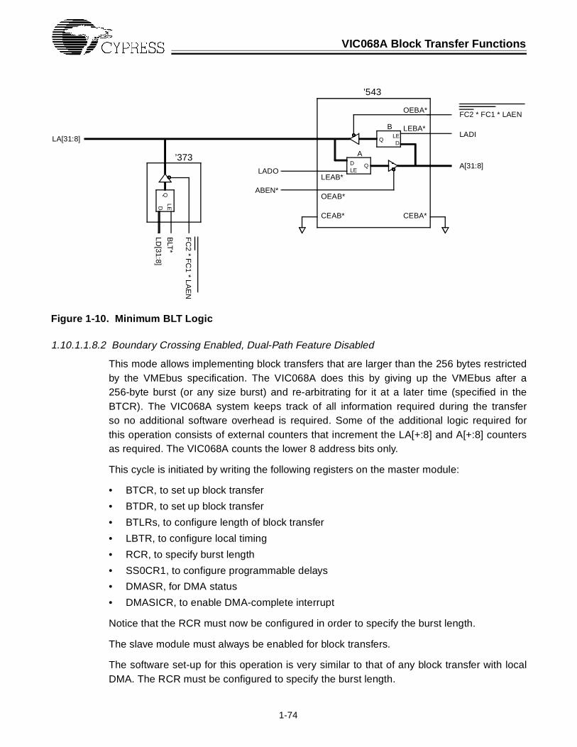
VIC068A Block Transfer Functions
1-74
Figure 1-10. Minimum BLT Logic
1.10.1.1.8.2 Boundary Crossing Enabled, Dual-Path Feature Disabled
This mode allows implementing block transfers that are larger than the 256 bytes restrictedby the VMEbus specification. The VIC068A does this by giving up the VMEbus after a256-byte burst (or any size burst) and re-arbitrating for it at a later time (specified in theBTCR). The VIC068A system keeps track of all information required during the transferso no additional software overhead is required. Some of the additional logic required forthis operation consists of external counters that increment the LA[+:8] and A[+:8] countersas required. The VIC068A counts the lower 8 address bits only.
This cycle is initiated by writing the following registers on the master module:
• BTCR, to set up block transfer
• BTDR, to set up block transfer
• BTLRs, to configure length of block transfer
• LBTR, to configure local timing
• RCR, to specify burst length
• SS0CR1, to configure programmable delays
• DMASR, for DMA status
• DMASICR, to enable DMA-complete interrupt
Notice that the RCR must now be configured in order to specify the burst length.
The slave module must always be enabled for block transfers.
The software set-up for this operation is very similar to that of any block transfer with localDMA. The RCR must be configured to specify the burst length.
LA[31:8]
FC2 * FC1 * LAEN
LADI
A[31:8]
FC
2 * FC
1 * LAE
N
BLT
*
LD[31:8]
’373
’543
B
A
OEBA*
LEBA*
CEBA*CEAB*
OEAB*
LEAB*
DLE
Q
LED
Q
LADO
ABEN*
LEDQ

VIC068A Block Transfer Functions
1-75
1.10.1.1.8.2.1 Sample 68K Code (write)
If we assume that the VIC068A registers are at vic_reg, as in the previous example, a sampleof 68K code that would configure the VIC068A for a block transfer with local DMA and boundarycrossing could be as follows:
; Set up VIC068A to block transfer 512 ; bytes in the BTLRs.
move.b #$02, (vic_reg, $db) move.b #$00, (vic_reg, $df)
; ; Specify a burst length of 64 cycles ; in the RCR ; ($00 specifies 64 cycles)
move.b #$00, (vic_reg, $d3) ; ; Enable boundary crossing for both ; the local bus and the VMEbus. ; Disable dual path. Use the BTDR
move.b #$0c, (vic_reg, $ab) ; ; Configure the local bus timing for: ; PAS* asserted time = 90ns ; PAS* deasserted time = 45ns ; DS* deasserted time = 15ns ; in the LBTR.
move.b #$44, (vic_reg, $a7) ; ; Configure for: ; interleave period = 0 ; write to VMEbus ; and enable block transfer w/ local ; DMA using the BTCR.
move.b #$40, (vic_reg, $d7)
As in any block transfer with local DMA, the VMEbus is requested at the assertion ofMWB*. In the above example, two bursts of 256 bytes (64 cycles of longwords) are per-formed. Between these bursts, an interleave time of “0” was specified. In this case, theVMEbus is immediately requested after it is given up after the first burst and the local buswill not be released. If a VMEbus master cycle is attempted during the interleave period,it will be DEDLKed (dual-path is not enabled).
The block transfer could be started as in any of the previous examples. Program theVIC068A to issue an interrupt or check for the completion of the transfer with the DMASR.
Notice that no additional software overhead is required (with the exception of writing theRCR) to perform a boundary crossing block transfer.

VIC068A Block Transfer Functions
1-76
1.10.1.1.8.3 Boundary Crossing Enabled, Dual-Path Enabled
This mode of operation is similar to that of the previous example except that master cyclesare allowed during the interleave period. If a master cycle is desired (MWB* asserted),the VMEbus is requested and the transfer takes place like any other master cycle. Arequest for a master cycle is DEDLKed if dual-path is not enabled.
The same registers that were used in the previous example are used in this example.Namely:
• BTCR, to set up block transfer
• BTDR, to set up block transfer
• BTLRs, to configure length of block transfer
• LBTR, to configure local timing
• RCR, to specify burst length
• SS0CR1, to configure programmable delays
• DMASR, for DMA status
• DMASICR, to enable DMA-complete interrupt
The required software set-up is no different from that of any block transfer with local DMAexcept that the dual-path bit (BTDR[0]) must be enabled.
1.10.1.1.8.3.1 Sample 68K Code (Write)
A sample of 68K code that would configure the VIC068A for a block transfer with localDMA with boundary crossing and dual-path could be as follows:
; Set up VIC068A to block transfer 512 ; bytes in the BTLRs.
move.b #$02, (vic_reg, $db) move.b #$00, (vic_reg, $df)
; ; ; Specify a burst length of 64 cycles ; in the RCR. ; ($00 specifies 64 cycles)
move.b #$00, (vic_reg, $d3) ; ; Enable boundary crossing for both ; the local bus and the VMEbus. ; Disable dual path. Use the BTDR.
move.b #$0d, (vic_reg, $ab) ; ; Configure the local bus timing for: ; PAS* asserted time = 90ns ; PAS* deasserted time = 45ns ; DS* deasserted time = 15ns ; in the LBTR.

VIC068A Block Transfer Functions
1-77
move.b #$44, (vic_reg, $a7) ; ; Configure for: ; interleave period = 1000ns ; write to VMEbus ; and enable block transfer w/ local ; DMA using the BTCR.
move.b #$44, (vic_reg, $d7)
The VMEbus is requested at the assertion of MWB*.
In this scenario, a block transfer of 512 bytes is performed in two blocks of 256 bytes.During the interleave period (1000 ns), master cycles can be performed.
1.10.1.1.9 D16 Block Transfers
The VIC068A is capable of performing D16 block transfers. If the WORD* signal is assertedduring the initiation cycle, the VIC068A performs the block transfer with D16 protocol onthe VMEbus.
The SWDEN* and ISOBE* signals can be configured to alternately toggle between thelower and the upper word banks, or swap all data to the upper word bank. If SS0CR0[4](D32 enable) is set, SWDEN* and ISOBE* will toggle for 32-bit memory. If it is cleared,the data will not switch between the upper and lower banks; only SWDEN* is asserted.
1.10.1.1.10 Data Acquisition Delays
The programmable delays in SS0CR1 take on different meanings depending on whetherthe system is reading, writing, or even whether it is the first transfer or subsequent transfers.During block transfer writes, the MBAT timing reflects the minimum delays. The actualdelays will depend on the speed in which DTACK* for the previous cycle is asserted. Noticethat the VIC068A asserts the DS* signals before the DTACK* signal has been assertedin an attempt to read-ahead the next data. During the read-ahead cycle, the VIC068Acannot deassert the LEDO and DS* signals before DTACK* is asserted from the previouscycle.
Master Write Block Transfer (MBAT1/0)
DSACKi*(L) & DS*(L) to DS*(H) DSACKi*(L) & DS*(L) to LEDO(H) DSACKi*(L) & DS*(L) to DSi*(L) DSACKi*(L) & DS*(L) to LA(7:0)
Master Read Block Transfer (MBAT1/0)
DSACKi*(L) & DS*(L) to DS*(H) DSACKi*(L) & DS*(L) to LEDI(H) DSACKi*(L) & DS*(L) to DSi*(L) DSACKi*(L) & DS*(L) to LA(7:0)

VIC068A Block Transfer Functions
1-78
The terms MBAT refer to the following bit fields:
MBAT0 = SSiCR1[3:0]MBAT1 = SSiCR1[7:4]
Figures 1-11 through 1-15 demonstrate these delays. See Chapter 1.13 for the actual ACperformance specifications.
1.10.1.2 MOVEM Block Transfers
The MOVEM block transfer is one in which the local CPU continues to be the local busmaster. The VMEbus block transfer protocol is the same as it was for block transfers withlocal DMA. This cycle is initiated by writing the registers:
• RCR, to configure burst length
• BTCR, to configure block transfer
Once BTCR[5] is set, the first assertion of MWB* qualified with the assertion of PAS*,causes the VIC068A to start the MOVEM transfer. The MOVEM block transfer will termi-nate if any of the following occur:
• BTCR[5] is cleared
• BERR* is asserted
• any local bus cycle occurs in which MWB* is not asserted
BTLR1/0 are not used for MOVEM block transfers. During MOVEM block transfers, thereis no latching of addresses. The VIC068A passes the local address onto the VMEbusaddress lines directly.
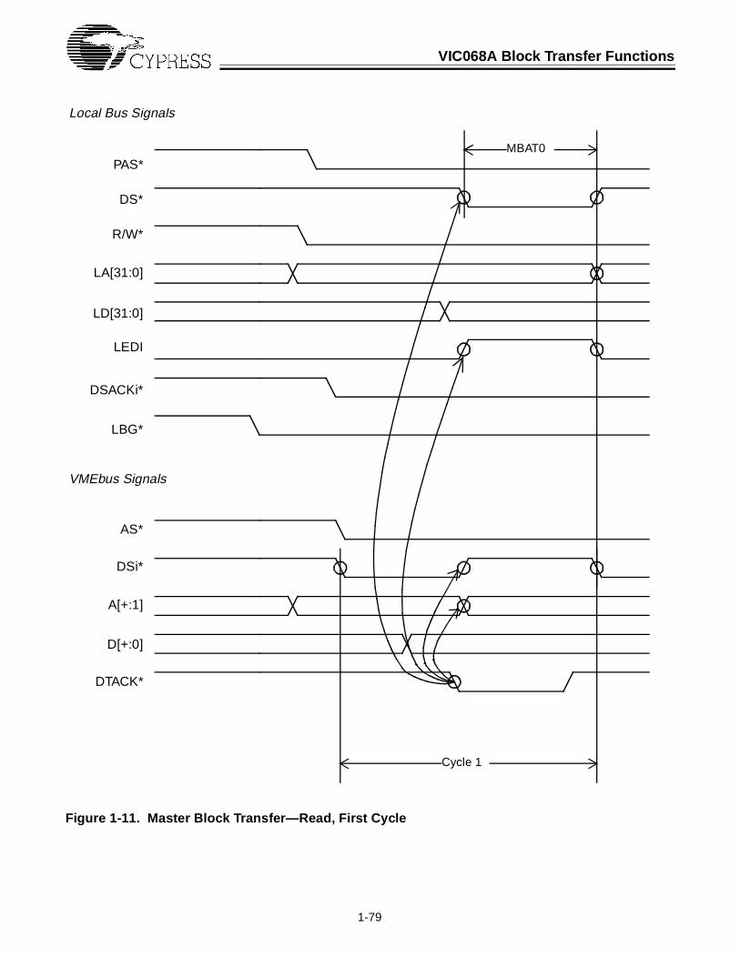
VIC068A Block Transfer Functions
1-79
Figure 1-11. Master Block Transfer—Read, First Cycle
Cycle 1
MBAT0PAS*
DS*
DTACK*
LA[31:0]
LD[31:0]
R/W*
DSACKi*
LEDI
AS*
DSi*
A[+:1]
D[+:0]
Local Bus Signals
VMEbus Signals
LBG*

VIC068A Block Transfer Functions
1-80
Figure 1-12. Master Block Transfer—Read, Second and Subsequent Cycles
Cycle N
PAS*
DS*
DTACK*
LA[31:0]
LD[31:0]
R/W*
DSACKi*
LEDI
AS*
DSi*
A[+:1]
D[+:0]
Local Bus Signals
VMEbus Signals
LBG*
MBAT1 MBAT1
COMPLETION OF CYCLE N-1
(N>2)

VIC068A Block Transfer Functions
1-81
Figure 1-13. Master Block Transfer—Write, First Cycle
PAS*
DS*
DTACK*
LA[31:0]
LD[31:0]
R/W*
DSACKi*
LEDO
AS*
DSi*
A[+:1]
D[+:0]
Local Bus Signals
VMEbus Signals
LBG*
Cycle 1
MBAT0
DST

VIC068A Block Transfer Functions
1-82
Figure 1-14. Master Block Transfer—Write, Second and Subsequent Cycles (Fast Sl ave)
Cycle N
PAS*
DS*
DTACK*
LA[31:0]
LD[31:0]
R/W*
DSACKi*
LEDO
AS*
DSi*
A[+:1]
D[+:0]
Local Bus Signals
VMEbus Signals
LBG*
MBAT1
DST
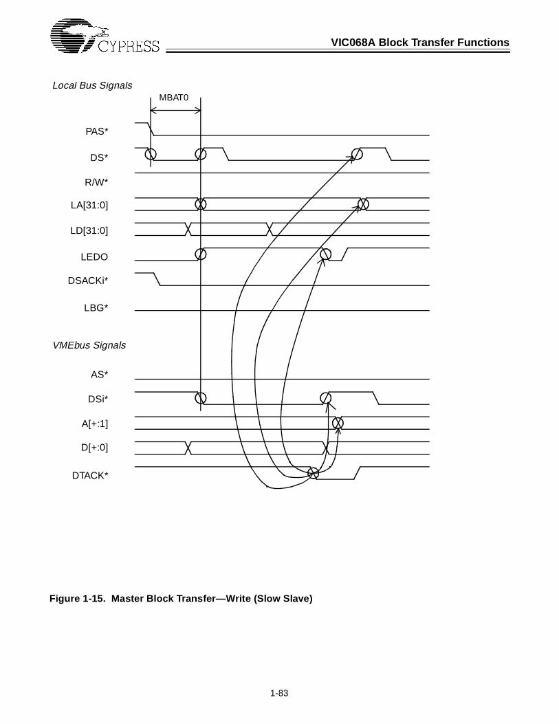
VIC068A Block Transfer Functions
1-83
Figure 1-15. Master Block Transfer—Write (Slow Slave)
PAS*
DS*
DTACK*
LA[31:0]
LD[31:0]
R/W*
DSACKi*
LEDO
AS*
DSi*
A[+:1]
D[+:0]
Local Bus Signals
VMEbus Signals
LBG*
MBAT0

VIC068A Block Transfer Functions
1-84
1.10.1.2.1 Sample MOVEM 68K Code
If, for example, we assume the VIC068A registers start at the base address vic_reg, asample of 68K code that would configure a MOVEM block transfer and dump the word contents ofthe 68K d0 through d7 registers to memory could be as follows:
; Write burst length in to the RCR. move.b #$0f, (vic_reg, $d3)
; ; Set the MOVEM bit in the BTCR.
move.b #$20, (vic_reg, $d7) ; ; Perform the MOVEM instruction. ; (a0 contains the destination ; address)
movem.l 0xffff, (a0) ; ; Clear the MOVEM bit.
move.b #$00, (vic_reg, $d7)
1.10.1.3 Buffer Control Signals During Master Block Transfers
The buffer control signals provide latching and bus-driving control for the address anddata lines on both local and VMEbus sides. For MOVEM block transfers, the buffer controlsignals are identical in behavior to that of normal master transfers. For block transfers withlocal DMA, the behavior of the buffer control signals may act slightly differently. Whenusing block transfers with local DMA, the loading, holding, and incrementing of the addresscounters and latches is controlled by LADO, ABEN* and the FC2/1 function codes.
Initialization Cycle
LADO is asserted as a result of PAS*, DS*, and MWB* being asserted for the initiationcycle.
VMEbus Read (Local Write)
LEDI is asserted as a result of the VMEbus DTACK* being asserted by the slave, indicatingthat valid data is available on the VMEbus. LEDI is deasserted as a result of MBAT1/0expiring.
VMEbus Write (Local Read)
During block transfer writes, the MBAT timing reflects the minimum delays. The actualdelays will depend on the speed in which DTACK* for the previous cycle is asserted. TheVIC068A asserts the DS* signal before the DTACK* signal has been asserted in an attemptto read-ahead the next data. During the read-ahead cycle, the VIC068A cannot deassertthe LEDO and DS* signals before DTACK* is asserted from the previous cycle.

VIC068A Block Transfer Functions
1-85
1.10.1.4 Performing Block Transfers to VMEbus Slaves Not Supporting Block
Transfers
The VIC068A may be used to perform block transfers with local DMA to cards that do notaccept block transfers. This is accomplished by performing the block transfer in bursts of1 and using single-cycle AM codes (set BTDR[1]). This makes the VMEbus data appearto be single-cycle data, but data is transferred on the local bus by DMA. Because theVIC068A is in a block transfer mode, the LADO signal operates by deasserting after DS*is asserted (recall that the address for single-cycle transfers must be held for the durationof the cycle, but for block transfers the slave is responsible for latching the address at thebeginning of the cycle). When the VIC068A is configured for bursts of 1, LADO may beconfigured to behave differently depending on certain register configurations. If BTDR[3]is set (VMEbus boundary crossing enabled), LADO is deasserted when DSi* is assertedfor the final transfer. If BTDR[3] is clear, LADO will hold until the final DTACK* of the finaltransfer. Therefore, it is recommended that boundary crossing be disabled when perform-ing these burst-of-1 transfers to non-block slaves.
1.10.2 VIC068A Slave Block Transfers
The VIC068A as a slave may be configured, in SSiCR0, to perform in one of three modesfor block transfers:
• does not support block transfers
• supports block transfers, but emulates single-cycle transactions on the local slave side(toggle PAS* and DSACKi* for each transfer)
• supports block transfers in a DMA-type mode where PAS* and DSACKi* are assertedthroughout the cycle and not toggled (accelerated transfers)
The VIC068A contains a slave block-transfer address counter separate from either of theaddress counters used for master block transfers. This counter, initialized by the VMEbusaddress, drives the local bus during the slave block transfer, and is incremented by theamount of data transferred with each local acknowledgment.
The timing for the slave’s response to a block transfer is the same for that of a masterblock transfer with local DMA. VIC068A registers relevant to slave block transfers are asfollows:
• Slave Select Control Registers (SS0CRi, SS1CRi)
• Local Bus Timing Register (LBTR)
The DMASR, DMASIR, RCR, BTCR, and the BTLRs are not used for slave block transfers.Slave block transfers that cross 256-byte boundaries are not supported in accordancewith the VMEbus specification.
VIC068A Block Transfer Functions
1-86
1.10.3 Buffer Control Signals During Slave Block Trans-fers
When the VIC068A is selected as a valid slave, LADI is asserted to latch the first address.From that point on, the VIC068A increments the lower 8 local address bits for each transfer.The data latches work as follows:
VMEbus Write (Local Write)
LEDI is asserted as a result of the VMEbus DSi* being asserted. LEDI is deasserted asa result of SBAT1/0 expiring.
VMEbus Read (Local Read)
Similar to master block transfer writes, the VIC068A attempts to read ahead the next datawhile the cycle is completing on the VMEbus. If DSi* from the previous cycle is not deas-serted before SBAT1 expires for the read-ahead cycle, LEDO and DS* are deasserted atthe deassertion of DSi*. If DSi* is deasserted before SBAT1 expires, LEDO and DS* aredeasserted at that point.
1.10.4 Using the CY7C964 for Additional Block Transfer Support
The CY7C964s are perfect companion chips for designs for which all of the VAC068A’sfunctionality is not required, or for designs that cannot incorporate the VAC068A’s addressmapping.
The CY7C964 provides all logic necessary for
• local boundary crossing
• VMEbus boundary crossing
• dual-path functionality
See Section 4, The CY7C964 Bus Interface Logic Circuit, for details on a VIC068A/CY7C964 interface.

VIC068A Block Transfer Functions
1-87
Figure 1-16. Slave Block Tran sfer—Read, First Cycle
PAS*
DS*
DTACK*
LA[31:0]
LD[31:0]
R/W*
DSACKi*
LEDO
AS*
DSi*
A[+:1]
D[+:0]
Local Bus Signals
VMEbus Signals
LBG*
SLSEL1*
LBR*
Cycle N
SBAT1

VIC068A Block Transfer Functions
1-88
Figure 1-17. Slave Block Tran sfer—Read, Sec ond and Subsequent Cycles
PAS*
DS*
DTACK*
LA[31:0]
LD[31:0]
R/W*
DSACKi*
LEDO
AS*
DSi*
A[+:1]
D[+:0]
Local Bus Signals
VMEbus Signals
LBG*
SLSEL1*
LBR*
COMPLETION OF CYCLE N–1
(N>2)Cycle N
SBAT1
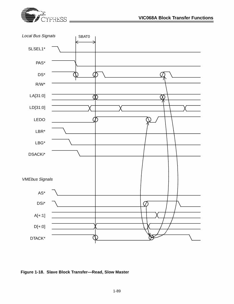
VIC068A Block Transfer Functions
1-89
Figure 1-18. Slave Block Tran sfer—Read, Slow Master
PAS*
DS*
DTACK*
LA[31:0]
LD[31:0]
R/W*
DSACKi*
LEDO
AS*
DSi*
A[+:1]
D[+:0]
Local Bus Signals
VMEbus Signals
LBG*
SLSEL1*
LBR*
SBAT0

VIC068A Block Transfer Functions
1-90
Figure 1-19. Slave Block Tran sfer—Write, First Cycle
PAS*
DS*
DTACK*
LA[31:0]
LD[31:0]
R/W*
DSACKi*
LEDO
AS*
DSi*
A[+:1]
D[+:0]
Local Bus Signals
VMEbus Signals
LBG*
SBAT0
Cycle 1
SLSEL1*
LBR*

VIC068A Block Transfer Functions
1-91
Figure 1-20. Slave Block Tran sfer—Write, Sec ond and Subsequent Cycles
PAS*
DS*
DTACK*
LA[31:0]
LD[31:0]
R/W*
DSACKi*
LEDI
AS*
DSi*
A[+:1]
D[+:0]
Local Bus Signals
VMEbus Signals
LBG*
SBAT1
Cycle N
SLSEL1*
LBR*

1-92
1.11Miscellaneous Features
This chapter describes additional miscellaneous features of the VIC068A.
1.11.1 Resetting the VIC068A
The VIC068A is reset by any of three distinct reset conditions. These reset conditions areinitiated by asserting various inputs or, in the case of a system reset, writing a VIC068Aregister. Since it is possible for more than one reset condition to be present simultaneously,the resets have the following priority:
1. global reset
2. internal reset
3. system reset
Upon completion of a VIC068A reset, ICR6[6] is set, thus causing SYSFAIL* to be as-serted. To remove the SYSFAIL* set ICR7[7], which is cleared by a global or power-upreset.
IMPORTANT
It is vital to the proper operation of the VIC068A that a global reset be performed at power-up. It is not necessary to wait for a system reset (caused by an assertion of SYSRESET*on the VMEbus) to complete before asserting a global reset. See section 1.11.1.2.
1.11.1.1 Internal Reset
The internal reset is the most common and easiest to implement of the VIC068A resets.This resets all the VIC068A internal circuitry and selected register bit fields. This reset istypically used as a push-button reset after power-up.
The internal reset is initiated by asserting the IRESET* signal for a minimum of 20 ns.Immediately after the assertion of IRESET*, the VIC068A asserts the LBR* signal. TheVIC068A then waits 1 ms for the assertion of LBG*. If LBG* is asserted within the 1-µstimeout, the VIC068A asserts HALT* and RESET* immediately. If LBG* is not assertedwithin this timeout period, the VIC068A asserts HALT* and RESET* as if LBG* had beenreceived. The VIC068A attempts this reset handshaking sequence to provide an orderlyreset of local resources.
After the VIC068A asserts HALT* and RESET*, the VIC068A deasserts LBR*, places allthree-state outputs to a high-Z state, and begins a 200-ms timeout period. If IRESET* is

Introduction to the VIC068A
1-93
still asserted after this timeout expires, the VIC068A begins an additional 200-ms timeout.The reset does not complete until the 200-ms timeout expires after IRESET* is deasserted.
If the VIC068A is the VMEbus system controller, the VIC068A also asserts SYSRESET*with the RESET* and HALT* signals.
After the conclusion of an internal reset, the HALT* and RESET* signals (and SYSRESET*if VMEbus is system controller) are deasserted and all outputs are brought to their quies-cent states.
1.11.1.2 Global Reset
The global reset provides the most complete reset to the VIC068A. This resets all VIC068Ainternal circuitry and all register bit fields to predefined states. A global reset must beissued at power-up to insure proper operation of the VIC068A.
The global reset is initiated by asserting the IPL0 signal after the IRESET* signal isasserted. It is important that IPL0 be asserted 16 ns (commercial) or 20 ns (industrial/military) after the IRESET* signal. This allows IRESET* to reverse the direction of theIPL0 line to an input. For a reliable global reset, the IPL0 signal should be asserted for aminimum of 50 ns.
Two notes should be observed when using global resets:
• SYSCLK is not driven while IPL0 is being asserted.
• The BGiOUT* daisy-chain is disconnected during the global reset.
The characteristics of the global reset are present only while IPL0 is asserted. This impliesthat the aforementioned behaviors are present only during the time IPL0 is asserted.Before the IPL0 signal is asserted, the VIC068A is in an internal reset state. After IPL0 isasserted, the VIC068A is in an internal reset state except that the registers have alreadyhad their bit fields set to their default global reset state.
If a global reset is needed when the VIC068A is configured as VMEbus system controller,assert IPL0 for a minimum time. This causes SYSCLK to be disabled only for the minimumtime IPL0 is asserted. The same is true for the BGiOUT* daisy-chain behavior.
The global reset mechanism is identical to the internal reset (LBG* and HALT* or RESET*timeouts, etc.) with the following two exceptions:
• All register bit fields are set to their default states.
• If the IPL0 signal is deasserted first (i.e., before IRESET*), the reset continues until a200-ms timeout expires.
• If the IRESET* signal is deasserted first (i.e., before IPL0), the reset concludes imme-diately instead of waiting for the 200-ms timeout to expire.
SYSRESET* is asserted during a global reset when configured as VMEbus system con-troller, as it is during an internal reset.

Introduction to the VIC068A
1-94
1.11.1.3 System Reset
The system reset is a VMEbus-defined reset that is signaled by the assertion of theVMEbus signal SYSRESET*. The system reset is typically issued from another moduleto reset an entire VMEbus system. The system reset resets all the VIC068A internalcircuitry and selected register bit fields. The VIC068A may both issue and receive a systemreset. If the VIC068A issues a system reset, it also resets itself.
There are two ways to issue a system reset:
• Write the SRCR with the value of $F0.
• Implement an internal or global reset while configured as a VMEbus system controller.
The VIC068A receives a system reset by having its SYSRESET* signal asserted. Whenthis occurs, the VIC068A begins the same procedures as if an internal reset had beenperformed.
The system reset is identical in function to the internal reset with the following exceptions:
• The effect on certain VIC068A register bit fields are different.
• If SYSRESET* is asserted beyond the 200-ms timeout described by the internal reset,the reset completes immediately after SYSRESET* is deasserted.
If an internal or global reset is performed on a system controller VIC068A while SYSRE-SET* is being asserted by another board, the VIC068A will not assert SYSRESET*. Thisimplies that any SYSRESET* asserted to a system controller VIC068A should be assertedfor the 200 ms required by the VMEbus specification.
1.11.1.4 Power-On Reset
To reliably reset the VIC068A at power-on, a global reset must be performed. In addition,the VIC068A must be in a “stable” operating environment at the initiation of the reset. Astable operating environment is defined by the following conditions:
• VCC has reached 5V dc.
• The CLK64M signal is within the specified operating range (see Chapter 1.16).
• All inputs are in a negated state (excluding address/data buses).
If the VIC068A is not in a stable environment when IRESET* is asserted, the VIC068Amay not reset reliably. If the power-on reset is performed when the environment is notstable, re-issue the global reset when the environment is stable.
Because a global reset causes certain VMEbus system controller operations to be sus-pended (see section 1.11.1.2), the power-on reset circuitry must be designed to assert theIPL0 signal for a “minimum” time while the VIC068A is the VMEbus system controller. Minimumis defined to be greater than the required 50 ns but less than the time the disabled featuresare required to be enabled for a particular application.

Introduction to the VIC068A
1-95
1.11.2 The Local Bus Timeout Timer
The VIC068A contains a local bus timeout timer that may be used to time certain localtimeout conditions for the local bus. The timer begins on the assertion of DS*. If the timerperiod expires without an assertion of either the DSACKi* or LBERR* signals, the VIC068Aasserts LBERR* and sets BESR[3].
The local timeout timer may be configured to include or not include time waiting for VMEbusacquisition. If enabled to include VMEbus acquisition time, BESR[0] is set when a timeoutoccurs. Once VMEbus mastership is obtained, the local timeout timer is reset and doesnot expire. At this point a VMEbus timeout timer (if one exists for the particular VMEbussystem) is used to indicate timeout conditions. If the VIC068A is used as the systemcontroller, this VMEbus timeout timer is located internal to the VIC068A.
If the local timeout timer is configured not to include VMEbus acquisition time, the timerresets at the assertion of BRi* and does not expire.
The local bus timeout periods are configurable for 4, 16, 32, 64, 128, 256, and 512 ms.
1.11.3 The DRAM Refresh Controller
The VIC068A contains a DRAM refresh controller. When enabled in the ARCR, theVIC068A increments a DRAM refresh counter every 15 µs. When the count of this counterreaches 4, the VIC068A requests the local bus by asserting LBR*. After the local bus isgranted, the VIC068A performs a CAS-before-RAS refresh (that is, DS*-before-PAS*).The VIC068A increments the refresh counter until the local bus is granted so the actualnumber of cycles that are performed would equal the number in the refresh counter whenthe local bus is granted to the VIC068A. If a VMEbus slave request is pending, the VIC068Agives priority to the slave transfer and the DRAM refresh is performed after the slavetransfer is complete, but within the same assertion of LBR*.
When the VIC068A receives the local bus, the VIC068A drives the FC2/1 signals with theDRAM refresh function codes. It then asserts PAS* and DS* according to the timingconfigured in the LBTR. Insure that the minimum High time specified for PAS* is greaterthen the minimum precharge time for the particular DRAMs being used. The VIC068Adrives the LA[7:0] signals High and asserts LAEN when performing DRAM refresh. TheSIZ1/0 signals are driven with a 32-bit code.
The refresh counter is a modulo-64 counter. If it reaches 64 without having the VIC068Aobtain the local bus, DRAM refresh cycles may be lost. The VIC068A local bus timer maybe used to insure that DRAM refresh cycles are not lost due to excessive local bus latency.

Introduction to the VIC068A
1-96
1.11.4 Rescinding Outputs
The VIC068A contains selected output signals that utilize a rescinding feature. A rescind-ing output is a three-state output driver that first drives the output High before three-stating.This is necessary for proper functionality of high-speed buses. The VIC068A rescindingoutputs are as follows:
VMEbus Local bus
DTACK* PAS* AS* DS* LWORD* LBERR* WRITE* R/W* BERR* SIZ1/0* IACK* FC2/1* DS1/0* BBSY*
1.11.5 Turbo Mode
By setting ICR[1], it is possible to reduce certain delays within the VIC068A. When set,the VIC068A reduces the following by 1 CLK64M period:
• VMEbus address set-up time
• VMEbus data set-up time
• DTACK* asserted time for slave block transfers
Because VMEbus times may be violated with this mode enabled, this mode should beused with caution.
1.11.6 Metastability Delays
Because the VMEbus is an asynchronous bus (the local bus may also be), the VIC068Amust insure that its synchronous logic is protected from possible metastable conditions.The VIC068A accomplishes this using a traditional double-sampling latch. The VIC068Asamples an input, then a specified settling time later samples it again. This allows for anymetastability that may have occurred to settle to a stable value. This settling time is pro-grammable to 3T or 4T in the ICR.

1-97
1.12VIC068A Register Map and
DescriptionsThis chapter describes the VIC068A internal configuration registers. These registers en-able and disable various features of the VIC068A. (Refer to the specific sections of thisguide for details on specific features.)
Table 1-16 provides information on the various reset states of the VIC068A registers. Thefollowing notes should be observed regarding this table:
• An asterisk (*) indicates a bit that is not affected by the particular reset.
• An “X” indicates a bit that is affected by that state of a particular VIC068A pin.
• ICR5 is the VIC068A-version register. Its contents will vary depending on the revisionof the device being used.
Unless otherwise specified, the reset status is given in this chapter by the values locatedin the parentheses by each bit field. The (X/X/X) format indicates the Global/Internal/System reset state of each bit or bit field.
For compatibility with the VIC64, it is recommended that all reserved register bits be writtenwith a 0.
Table 1-16. VIC068A Register Values After Reset Operations
Address(hex) Name Description
GlobalReset
InternalReset
SystemReset
03 VIICR VMEbus Interrupter Interrupt Control Register 11111000 11111*** 11111***
07–1F CICR1–7 VMEbus Interrupt Control Registers 1–7 11111000 11111*** 11111***
23 DMASR DMA Status Register 11111000 11111*** 11111***
27–3F LICR1–7 Local Interrupt Control Registers 1–7 1000X000 1***X*** 1***X***
43 ICGSICR ICGS Interrupt Control Register 11111000 11111*** 11111***
47 ICMSICR ICMS Interrupt Control Register 11111000 11111*** 11111***
4B EGICR Error Group Interrupt Control Register 1111X000 1111X*** 1111X***
4F ICGSVBR ICGS Vector Base Register 000011XX 000011XX 000011XX
53 ICMSVBR ICMS Vector Base Register 000011XX 000011XX 000011XX
57 LIVBR Local Interrupt Vector Base Register 00001XXX 00001XXX 00001XXX
5B EGIVBR Error Group Interrupt Vector Base Register 00001XXX 00001XXX 00001XXX
5F ICSR Interprocessor Communications Switch Register 00000000 ****0000 00000000
63–73 ICR0-4 Interprocessor Communications Registers 0–4 00000000 00000000 00000000
77 ICR5 Interprocessor Communications Register 5 Version Version Version
7B ICR6 Interprocessor Communications Register 6 X11111XX X1111111 X1111110
7F ICR7 Interprocessor Communications Register 7 00X00000 *0XX**** 00X00000
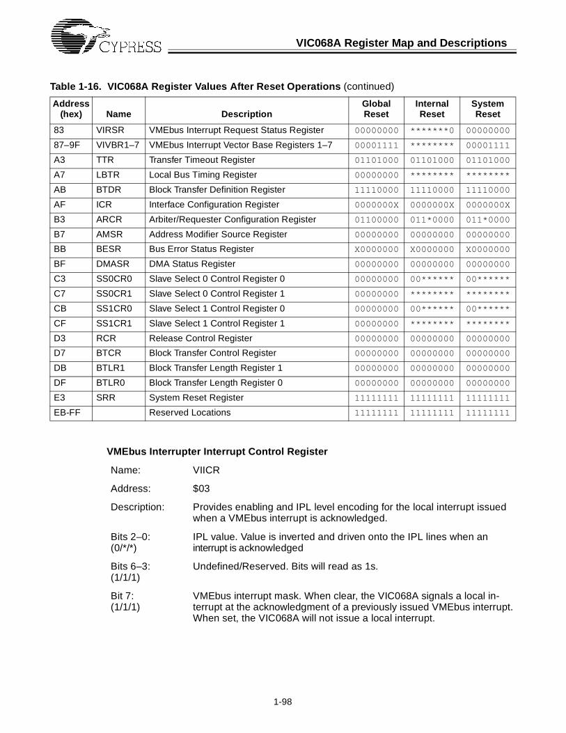
VIC068A Register Map and Descriptions
1-98
83 VIRSR VMEbus Interrupt Request Status Register 00000000 *******0 00000000
87–9F VIVBR1–7 VMEbus Interrupt Vector Base Registers 1–7 00001111 ******** 00001111
A3 TTR Transfer Timeout Register 01101000 01101000 01101000
A7 LBTR Local Bus Timing Register 00000000 ******** ********
AB BTDR Block Transfer Definition Register 11110000 11110000 11110000
AF ICR Interface Configuration Register 0000000X 0000000X 0000000X
B3 ARCR Arbiter/Requester Configuration Register 01100000 011*0000 011*0000
B7 AMSR Address Modifier Source Register 00000000 00000000 00000000
BB BESR Bus Error Status Register X0000000 X0000000 X0000000
BF DMASR DMA Status Register 00000000 00000000 00000000
C3 SS0CR0 Slave Select 0 Control Register 0 00000000 00****** 00******
C7 SS0CR1 Slave Select 0 Control Register 1 00000000 ******** ********
CB SS1CR0 Slave Select 1 Control Register 0 00000000 00****** 00******
CF SS1CR1 Slave Select 1 Control Register 1 00000000 ******** ********
D3 RCR Release Control Register 00000000 00000000 00000000
D7 BTCR Block Transfer Control Register 00000000 00000000 00000000
DB BTLR1 Block Transfer Length Register 1 00000000 00000000 00000000
DF BTLR0 Block Transfer Length Register 0 00000000 00000000 00000000
E3 SRR System Reset Register 11111111 11111111 11111111
EB-FF Reserved Locations 11111111 11111111 11111111
VMEbus Interrupter Interrupt Control Register
Name: VIICR
Address: $03
Description: Provides enabling and IPL level encoding for the local interrupt issued when a VMEbus interrupt is acknowledged.
Bits 2–0:(0/*/*)
IPL value. Value is inverted and driven onto the IPL lines when an interrupt is acknowledged
Bits 6–3:(1/1/1)
Undefined/Reserved. Bits will read as 1s.
Bit 7:(1/1/1)
VMEbus interrupt mask. When clear, the VIC068A signals a local in-terrupt at the acknowledgment of a previously issued VMEbus interrupt. When set, the VIC068A will not issue a local interrupt.
Table 1-16. VIC068A Register Values After Reset Operations (continued)
Address(hex) Name Description
GlobalReset
InternalReset
SystemReset

VIC068A Register Map and Descriptions
1-99
VMEbus Interrupt Control Registers 1–7
Name: VICR1–7
Addresses:For interrupt:
$07, $0B, $0F, $13, $17, $1B, $1F 1 2 3 4 5 6 7
Description: Provides enabling of the VIC068A as VMEbus interrupt handler for any or all of the VMEbus interrupts. Seven registers exist to provide unique masking and IPL values for the seven VMEbus interrupts.
Bits 2–0:(0/*/*)
IPL value. Value is inverted and driven onto the IPL signals when a VMEbus interrupt is acknowledged.
Bits 6–3:(1/1/1)
Undefined/Reserved. Bits will read as 1s.
Bit 7:(1/1/1)
VMEbus interrupt mask. When clear, the VIC068A acts as a VMEbus interrupt handler by signaling a local interrupt at the specified IPL level. When set, the VIC068A does not handle the VMEbus interrupt and no local interrupt is issued.
DMA Status Interrupt Control Register
Name: DMASICR
Address: $23
Description: Provides enabling and IPL-level encoding for the DMA-complete inter-rupt issued by the VIC068A when any VIC068A local DMA operation completes (successfully or unsuccessfully).
Bits 2–0:(0/*/*)
IPL value. Value is inverted and driven onto the IPL lines when interrupt is acknowledged.
Bits 6–3:(1/1/1)
Undefined/Reserved. Bits will read as 1s.
Bit 7:(1/1/1)
DMA status interrupt mask. When clear, the VIC068A signals a local interrupt at the completion of any VIC068A local DMA operation. When set, the VIC068A will not issue a local interrupt.
Local Interrupt Control Registers 1–7
Name: LICR1–7
Address:For LIRQ:
$27, $2B, $2F, $33, $37, $3B, $3F 1 2 3 4 5 6 7
Description: Provides enabling, IPL level, and control of local interrupts 1–7 (LIRQ1–7*).
Bits 2–0:(0/*/*)
IPL value. Value is inverted and driven onto the IPL lines when a local interrupt is presented on the LIRQ1–7* signals and bit 7 of this register is clear (enabled).
Bit 3:(X/X/X)
LIRQ1–7* voltage state. A cleared bit indicates the LIRQ1–7* signal is asserted at the VIC068A.

VIC068A Register Map and Descriptions
1-100
Bit 4:(0/*/*)
Autovector enable. When set, the VIC068A will supply the interrupt status/ID vector for the local interrupt acknowledge cycle. When cleared, the VIC068A will assert the LIACK0* signal to indicate an 68K “autovector” condition or that the interrupting source should provide the Status/ID vector to the processor.
Bit 5:(0/*/*)
Edge/level enable. When cleared, the VIC068A responds to the LIRQ1-7* as a level-sensitive interrupt. When set, the VIC068A responds to LIRQ1–7* as an edge-sensitive interrupt.
Bit 6:(0/*/*)
Polarity set. When set, the VIC068A responds to interrupts as active High if bit 5 is clear (level sensitive) or on a rising edge if bit 5 is set (edge sensitive). When clear, the VIC068A responds to interrupts as active Low if bit 5 is clear (level sensitive) or on a falling edge if bit 5 is set (edge sensitive).
Bit 7:(1/1/1)
Local interrupt mask. When clear, the VIC068A is enabled to handle the corresponding local interrupt asserted on the LIRQ1–7* signals.
ICGS Interrupt Control Register
Name: ICGSICR
Address: $43
Description: Provides enabling and IPL encoding for the four global switch inter-rupts.
Bits 2–0:(0/*/*)
IPL Value. Value is inverted and driven onto the IPL signals when a global switch is acknowledged.
Bit 3:(1/1/1)
Undefined/Reserved. Bit will read as a 1.
Bit 4:(1/1/1)
ICGS0 mask. When clear, the VIC068A will issue and handle a local interrupt when global switch 0 is set.
Bit 5:(1/1/1)
ICGS1 mask. When clear, the VIC068A will issue and handle a local interrupt when global switch 1 is set.
Bit 6:(1/1/1)
ICGS2 mask. When clear, the VIC068A will issue and handle a local interrupt when global switch 2 is set.
Bit 7:(1/1/1)
ICGS3 mask. When clear, the VIC068A will issue and handle a local interrupt when global switch 3 is set.
ICMS Interrupt Control Register
Name: ICMSICR
Address: $47
Description: Provides enabling and IPL encoding for the four module switch interrupts.
Local Interrupt Control Registers 1–7 (continued)
VIC068A Register Map and Descriptions
1-101
Bits 2–0:(0/*/*)
IPL Value. Value is inverted and driven onto the IPL signals when a module switch is acknowledged.
Bit 3:(1/1/1)
Undefined/Reserved. Bit will read as a 1.
Bit 4:(1/1/1)
ICMS0 mask. When clear, the VIC068A will issue and handle a local interrupt when module switch 0 is set.
Bit 5:(1/1/1)
ICMS1 mask. When clear, the VIC068A will issue and handle a local interrupt when module switch 1 is set.
Bit 6:(1/1/1)
ICMS2 mask. When clear, the VIC068A will issue and handle a local interrupt when module switch 2 is set.
Bit 7:(1/1/1)
ICMS3 mask. When clear, the VIC068A will issue and handle a local interrupt when module switch 3 is set.
Error-Group Interrupt Control Register
Name: EGICR
Address: $4B
Description: Provides enabling and IPL encoding for the error group interrupts.
Bits 2–0:(0/*/*)
IPL Value. Value is inverted and driven onto the IPL signals when an error group interrupt is acknowledged.
Bit 3:(X/X/X)
SYSFAIL* asserted. This bit is set whenever SYSFAIL* is detected asserted.
Bit 4:(1/1/1)
SYSFAIL* interrupt mask. When clear, the VIC068A generates a local interrupt when SYSFAIL* is asserted.
Bit 5:(1/1/1)
Arbitration timeout interrupt mask. When clear, the VIC068A generates a local interrupt when an arbitration timeout has occurred.
Bit 6:(1/1/1)
Write post fail interrupt mask. When clear, the VIC068A generates a local interrupt when a write post operation has failed due to a bus error. For master write posts, an assertion of BERR* will trigger an interrupt. For slave write posts, an assertion of LBERR* will trigger an interrupt.
Bit 7:(1/1/1)
AC Fail interrupt mask. When clear, the VIC068A generates a local interrupt when ACFAIL* is detected as asserted.
ICMS Interrupt Control Register (continued)

VIC068A Register Map and Descriptions
1-102
ICGS Interrupt Vector Base Register
Name: ICGSIVBR
Address: $4F
Description: Provides the status/ID vector for the global switch interrupts. This reg-ister must be written after any VIC068A reset to enable identification encoding for bits 1-0.
Bits 1–0:(X/X/X)
Global switch number (read-only). This value indicates which global switch is pending during a global switch interrupt acknowledge cycle. These bits are used with bits 7–2 to provide a unique status/ID vector for each global switch. The numeric value of this field indicates the switch number. These bits are valid only during the interrupt acknowl-edge cycle.
Bits 7–2: Status/ID. These bits are user-definable and are used with bits 1–0 to provide a unique global switch interrupt status/ID vector.
ICMS Interrupt Vector Base Register
Name: ICMSIVBR
Address: $53
Description: Provides the status/ID vector for the module switch interrupts. This register must be written after any VIC068A reset to enable identification encoding for bits 1-0. This register is reset to $F0 during any VIC068A reset.
Bits 1–0:(X/X/X)
Module switch number (read-only). This value indicates which module switch is pending during a module switch interrupt acknowledge cycle. These bits are used with bits 7–2 to provide a unique status/ID vector for each module switch. The numeric value of this field indicates the switch number. These bits are valid only during the interrupt acknowl-edge cycle.
Bits 7–2: Status/ID. These bits are user-definable and are used with bits 1–0 to provide a unique module switch interrupt status/ID vector.
Local Interrupt Vector Base Register
Name: LIVBR
Address: $57
Description: Provides the status/ID vector for the local interrupts. This register must be written after any VIC068A reset to enable identification encoding for bits 2–0. This register is reset to $F0 during any VIC068A reset.
VIC068A Register Map and Descriptions
1-103
Bits 2–0:(X/X/X)
Local Interrupt number (read-only). This value indicates which local interrupt is pending during a local interrupt acknowledge cycle. These bits are used with bits 7–3 to provide a unique status/ID vector for each local interrupt. The numeric value of this field indicates the local inter-rupt number. These bits are valid only during the interrupt acknowledge cycle.
Bits 7–3: Status/ID. These bits are user-definable and are used with bits 1–0 to provide a unique local interrupt status/ID vector.
Error Group Interrupt Vector Base Register
Name: EGIVBR
Address: $5B
Description: Provides the status/ID vector for the error group interrupts. This register must be written after any VIC068A reset to enable identification en-coding for bits 2–0. This register is reset to $F0 during any VIC068A reset.
Bits 2–0:(X/X/X)
Error/Status Group Interrupt number (read-only). This value indicates which group interrupt is pending during the interrupt acknowledge cy-cle. These bits are used with bits 7–3 to provide a unique status/ID vector for each error group interrupt. These bits are valid only during the interrupt acknowledge cycle.
Bits 2–0 Error/Status Interrupt
0 0 0 ACFAIL* asserted 0 0 1 Write post failed 0 1 0 Arbitration timeout 0 1 1 SYSFAIL* asserted 1 0 0 VMEbus Interrupter interrupt acknowledge 1 0 1 DMA complete
Bits 7–3: Status/ID. These bits are user-definable and are used with bits 1-0 to provide a unique interrupt status/ID vector.
Interprocessor Communications Switch Register
Name: ICFSR
Address: $5F
Description: Provides setting, clearing, and monitoring of the interprocessor switch interrupts via the local bus. If the switch interrupts are enabled, setting these bits (more precisely, a clear-to-set transition) causes a local in-terrupt to occur in the same way as if the switch was set over the VMEbus.
Bits 3–0:(0/0/0)
Module switches. Bits 0, 1, 2, and 3 correspond to ICMSs 0, 1, 2, and 3 respectively.
Bits 7–4:(0/*/0)
Global switches. Bits 4, 5, 6, and 7 correspond to ICGSs 0, 1, 2, and 3 respectively.
Local Interrupt Vector Base Register (continued)

VIC068A Register Map and Descriptions
1-104
Interprocessor Communication Registers 0–4
Name: ICR0–4
Addresses:For registers:
$63, $67, $6B, $6F, $73 0 1 2 3 4
Description: These are general-purpose read/write registers that can be accessed from either the local bus or the VMEbus. The addresses listed above are the local addresses. See Chapter 1.8 for details on accessing these registers from the VMEbus.
Bits 7–0:(0/0/0)
Data field.
Interprocessor Communication Register 5
Name: ICR5
Address: $77
Description: This register provides the VIC068A version/revision number. The first VIC068A device contains a value of $F1. Contact your local Cypress Semiconductor sales office for current VIC068A revision status. The address listed above is the local address. See Chapter 1.8 for details on accessing this register from the VMEbus.
Bits 7–0: VIC068A version/revision (read-only).
Interprocessor Communication Register 6
Name: ICR6
Address: $7B
Description: This register provides local or remote reset and HALT*. The address listed above is the local address. See Chapter 1.8 for details on accessing this register from the VMEbus.

VIC068A Register Map and Descriptions
1-105
Bits 1–0: Reset/HALT* status (read-only from VMEbus). These bits provide re-set/HALT* status of the VIC068A and local resources according to the following table:
Bits 1–0 Reset/HALT* Status.
0 1 HALT* has been asserted longer than 6 ms by a sourceother then the VIC068A. These bits may both be resetby the local CPU to indicate local resources are runningand operational.
1 0 The VIC068A has performed a local reset function andthe VIC068A is not the system controller. These bits mayboth be reset by the local CPU to indicate local resourcesare running and operational.
1 1 Indicates that the CPU has just been released from asystem reset.
0 0 Local resources are running and operational. This pat-tern must be written by the local CPU after a reset con-dition to indicate that local resources are running andoperational.
Bits 5–2:(1/1/1)
Undefined/Reserved. Bits will read as 1s.
Bit 6:(1/1/1)
IRESET* and HALT* status (read-only from VMEbus). This bit is set upon assertion of IRESET*, and/or HALT*. It is set whether HALT* is asserted by external sources or by the VIC068A. SYSFAIL* is asserted when this bit is set if the SYSFAIL* mask bit (ICR7, bit 7) is cleared.
Bit 7:(X/X/X)
IRESET* status (read-only). On a VMEbus read, this bit indicates that the VIC068A is in a reset state. On a local bus read, this bit is set whenever ACFAIL* is asserted.
Interprocessor Communication Register 7
Name: ICR7
Address: $7F
Description: This register provides semaphores to the five general-purpose inter-processor communication registers (ICR4–0). The remaining bits indi-cate VMEbus master status, generate HALT* and RESET*, and mask SYSRESET*. The address listed above is the local address. See Chap-ter 1.8 for details on accessing this register from the VMEbus.
Bits 4–0:(0/*/0)
ICR4–0 semaphores. These bits provide semaphores to the five inter-processor communication registers ICR4–0 respectively. Each bit is set when the corresponding ICR is written. These bits must be cleared by the user (i.e., they are not cleared automatically). These bits can be read or written from the local bus or the VMEbus.
Interprocessor Communication Register 6 (continued)

VIC068A Register Map and Descriptions
1-106
Bit 5:(X/X/X)
VMEbus master status (read-only). This bit is set whenever the VIC068A is the VMEbus master, and the VIC068A is asserting AS*. This bit is not set when the VIC068A is VMEbus master to an idle bus in ROR and BCAP release modes. Bit 7 of the BESR may be used to indicate that the VIC068A is VMEbus master when AS* is not asserted.
Bit 6:(0/0/0)
HALT* and RESET* control. This bit may be used to assert the HALT* and RESET* pins via software. Whenever this bit is set, the VIC068A asserts HALT* and RESET* until this bit is cleared or any reset occurs.
Bit 7:(0/*/0)
SYSFAIL* mask. When set, the VIC068A is prohibited from asserting SYSFAIL* in response to bit 6 of ICR6 being set (which, by default, is set after any reset). This bit must be written after resetting the VIC068A to deassert SYSFAIL*.
VMEbus Interrupt Request/Status Register
Name: VIRSR
Address: $83
Description: This register provides status and control of the VMEbus interrupts 7–1.
Bit 0:(0/0/0)
Register enable/disable. This bit provides enabling and disabling for the remainder of this register.
Bits 7–1:(0/0/0)
VMEbus interrupt switches. Setting any of these bits asserts the VME-bus IRQi* signals corresponding to the bit positions, if bit 0 is set during the write. These bits are cleared automatically when the interrupt is serviced.
VMEbus Interrupt Vector Base Registers 1–7
Name: VIVBR
Address:for IRQ:
$87, $8B, $8F, $93, $97, $9B, $9F 1 2 3 4 5 6 7
Description: Provides the status/ID vector for the VMEbus interrupts.
Bits 7–0: Status/ID Vector. These bits provide the status/ID vector for VMEbus interrupt acknowledge cycles. Address $87 corresponds to IRQ1*. These bits are set to a value of $0F for global and system resets and are unchanged by internal resets.
Transfer Timeout Register
Name: TTR
Address: $A3
Description: Provides control of the local and VMEbus timeout timers.
Interprocessor Communication Register 7 (continued)

VIC068A Register Map and Descriptions
1-107
Bit 0:(0/0/0)
Include VMEbus acquisition. When set, the local bus timer will include waiting for VMEbus acquisition. When clear, the local bus timer will stop and reset when the VMEbus is requested.
Bit 1:(0/0/0)
Arbitration timeout. When set, the VIC068A as VMEbus arbiter has detected a VMEbus arbitration timeout. This is only used when con-figured as the VMEbus system controller (SCON* asserted).
Bits 4–2: Local bus timeout period. Defines the local bus timeout.
Bit 4 Bit 3 Bit 2 Local Bus Timeout (ms)
0 0 0 4 0 0 1 16 0 1 0 32 (default)0 1 1 64 1 0 0 128 1 0 1 256 1 1 0 512 1 1 1 Infinite (timer disabled)
Bits 7–5: VMEbus timeout period. Defines the VMEbus timeout.
Bit 7 Bit 6 Bit 5 VMEbus Timeout (ms)
0 0 0 4 0 0 1 16 0 1 0 32 (default)0 1 1 64 1 0 0 128 1 0 1 256 1 1 0 512 1 1 1 Infinite (timer disabled)
Local Bus Timing Register
Name: LBTR
Address: $A7
Description: Provides timing control for PAS* and DS* signals when the VIC068A is local bus master. In the following descriptions, n is the binary value specified in the bit fields, and T is one CLK64M clock period. Clock latency may add one additional clock period to these times.
Bits 3–0:(0/*/*)
Minimum PAS* asserted time. This field specifies the minimum asserted time for the PAS* signal whenever the VIC068A is the local bus master. The time is specified by (n + 2)T. The actual asserted time depends on a number of factors including local and VMEbus acknowledge tim-ing.
Transfer Timeout Register (continued)

VIC068A Register Map and Descriptions
1-108
Bit 4:(0/*/*)
Minimum DS* deasserted time. This field specifies the minimum deas-serted time for the DS* signal whenever the VIC068A is the local bus master. A time of 1T is selected when this bit is clear; 2T is selected when this bit is set.
Bits 7–5:(0/*/*)
Minimum PAS* deasserted time. This field specifies the minimum deas-serted time for the PAS* signal whenever the VIC068A is the local bus master. The time is specified by (n + 1)T.
Block Transfer Definit ion Register
Name: BTDR
Address: $AB
Description: Configures master block transfers (both MOVEM and block transfers with local DMA) for boundary crossings, dual-path, and user-defined address modifiers. See Chapter 1.10 for more details on implementing these features.
Bit 0:(0/0/0)
Dual-path enable. When set, the VIC068A is enabled with the dual-path feature during master block transfers with local DMA. External logic is required when this option is enabled.
Bit 1:(0/0/0)
AMSR Enable. When set, the VIC068A will issue the AM codes based in the address modifier source register for block transfers. This bit effects the AM codes for block transfers only.
Bit 2:(0/0/0)
When this bit is set, it enables local address 256-byte boundary cross-ings during DMA block transfer operations. External logic is required to increment latched address lines when this option is enabled.
Bit 3:(0/0/0)
When this bit is set, it enables VMEbus address 256-byte boundary crossings during DMA block transfer operations. External logic is re-quired to increment latched address lines when this option is enabled.
Bit 7–4:(1/1/1)
Undefined/Reserved. Bits will be read as 1s.
Interface Configuration Register
Name: ICR
Address: $AF
Description: Controls various features of the VIC068A including RMCs, deadlock signaling, metastability delays, and the “turbo” feature.
Bit 0:(X/X/X)
SCON* value (read-only). Reads the value of the SCON* pin. When set, the VIC068A is not the VMEbus system controller. When clear, the VIC068A is the VMEbus system controller.
Local Bus Timing Register

VIC068A Register Map and Descriptions
1-109
Bit 1:(0/0/0)
Turbo enable. When set, the VIC068A accelerates VMEbus transfers by reducing selected timings by one CLK64M clock period. VMEbus protocols may be violated when the turbo mode is enabled (see section 1.11.5).
Bit 2:(0/0/0)
Metastability interval. When set, the VIC068A adds one additional CLK64M clock period of metastability delay on asynchronous inputs (from 3 CLK64M periods to 4).
Bits 4, 3:(0/0/0)
Deadlock signaling. These bits configure deadlock signaling. Bit 4 is used to enable the assertion of HALT* and LBERR* in addition to the DEDLK* signal in deadlock situations. If bit 4 is enabled, bit 3 may be used to prevent the assertion of HALT* for RMC deadlocks.
Bit 4 Bit 3 Deadlock Signaling
0 X DEDLK* only (default)1 0 HALT*, LBERR*, DEDLK* 1 1 HALT*, LBERR*, DEDLK*
(HALT* is not asserted for RMC cycles)
Bit 5:(0/0/0)
RMC control bit 1. When set, the VIC068A will request the VMEbus whenever the RMC* is asserted independent of the MWB* signal.
Bit 6:(0/0/0)
RMC control bit 2. When set, the VMEbus AS* is stretched when RMC* is asserted for VMEbus transfers.
Bit 7:(0/0/0)
RMC control bit 3. When set, the VIC068A qualifies the RMC control bits 5 and 6 with the SIZ1/0 signals. If RMC control bits 5 or 6 are set and the first cycle of the RMC transfer is of byte size, the “set” behaviors are not implemented.
Arbiter/Requester Configuration Register
Name: ARCR
Address: $B3
Description: This register provides configuration of the fairness timeout and DRAM refresh features. The VMEbus request level is also configured from this register.
Bits 3–0:(0/0/0)
Fairness timer enable. The VMEbus fair requester is enabled in this bit field according to the following table:
Bits 3–0 Timeout Period/Mode
$0 Fairness disabled (default)$F Timeout disabled All other patterns 2 µs times number
Bit 4:(0/*/*):
DRAM refresh. When set, the VIC068A will perform CAS-before-RAS (DS* before PAS*) refresh functions.
Interface Configuration Register (continued)

VIC068A Register Map and Descriptions
1-110
Bits 6, 5: VMEbus request level. The VMEbus request level is set according to the following table:
Bit 6 Bit 5 VMEbus Request Level
0 0 BR0 0 1 BR1 1 0 BR2 1 1 BR3 (default)
Bit 7:(0/0/0)
Arbitration mode. When set, the VIC068A performs priority VMEbus arbitration. When clear, the VIC068A performs round-robin arbitration. This bit is only relevant when the VIC068A is configured as the VMEbus system controller (SCON* asserted).
Address Modifier Source Register
Name: AMSR
Address: $B7
Description: This register provides the user-definable address modifiers (AM codes) that can be sourced by the VIC068A for VMEbus master cycles, or used in validating AM codes during VMEbus slave cycles.
Bits 5–0:(0/0/0)
Address modifier code. The AM code that is issued during master cycles or used for qualifying slave cycles. This register is used only when enabled for user-defined AM codes. Otherwise, standard VME-bus AM codes are used.
Bit 6:(0/0/0)
AM5–3 qualification. When set, the VIC068A uses bits 5–3 in qualifying for slave accesses in addition to the address space size information defined by bits 3 and 2 of the SSiCR0s. This bit is overridden if bits 3 and 2 of the SSiCR0s are both set.
Bit 7:(0/0/0)
AM2–0 generation. When set, the VIC068A issues the AM2–0 codes based on the FC2/1 signals. AM5–3 will be issued from bits 5–3 of this register.
Bus Error Status Register
Name: BESR
Address: $BB
Description: This register provides BERR*/LBERR*, self-access, VMEbus master-ship, and timeout status. All bits except bit 7 are flags that must be cleared manually by the local processor after being set by status con-ditions. If these bits are to be used for a specific operation, it is important that they be cleared prior to starting that operation.
Bit 0:(0/0/0)
Local timeout during VMEbus acquisition. This bit, when set, indicates that a local bus timeout has occurred during an attempted acquisition of the VMEbus.
Arbiter/Requester Configuration Register (continued)

VIC068A Register Map and Descriptions
1-111
Bit 1:(0/0/0)
SLSEL1* self-access. This bit is set when the VIC068A is selected by the assertion on the SLSEL1* signal, while operating as VMEbus mas-ter.
Bit 2:(0/0/0)
SLSEL0* self-access. This bit is set when the VIC068A is selected by the assertion on the SLSEL0* signal, while operating as VMEbus mas-ter.
Bit 3:(0/0/0)
Local bus timeout. This bit, when set, indicates a local bus timeout occurred without qualification.
Bit 4:(0/0/0)
VMEbus timeout. This bit, when set, indicates the VIC068A has sig-naled a VMEbus timeout. This bit is relevant only if the VIC068A is system controller and the VMEbus timeout is enabled.
Bit 5:(0/0/0)
VMEbus bus error. This bit is set when a VMEbus bus error is signaled (BERR* asserted).
Bit 6:(0/0/0)
Local bus error. This bit is set when a local bus error is signaled by a source other then the VIC068A (LBERR* asserted to the VIC068A).
Bit 7:(X/X/X)
VMEbus mastership. This bit is set whenever the VIC068A is VMEbus master.
DMA Status Register
Name: DMASR
Address: $BF
Description: This register provides status of a VIC068A DMA transfer. This includes the block transfer with local DMA function. Status bits are included to show various BERR* and LBERR* statuses and DMA termination sta-tuses.
Bit 0:(0/0/0)
Block transfer in progress. This bit, when set, indicates an interleaved block transfer is in progress. Once set, this bit is cleared automatically by the VIC068A after completion of the local DMA operation, or by resetting the VIC068A.
Bit 1:(0/0/0)
LBERR* during DMA transfer. This bit, when set, indicates a LBERR* was signaled during a DMA transfer. Once set, this bit must be cleared manually by writing a 0 (zero) to this bit location, or by resetting the VIC068A.
Bit 2:(0/0/0)
BERR* during DMA transfer. This bit, when set, indicates a BERR* was signaled during a DMA transfer. Once set, this bit must be cleared manually by writing a 0 (zero) to this bit location, or by resetting the VIC068A.
Bit 3:(0/0/0)
Local bus error (read-only). This bit is set when a local bus error is signaled by a source other then the VIC068A (LBERR* asserted to the VIC068A). This bit is a read-only copy of bit 6 of the BESR.
Bus Error Status Register (continued)

VIC068A Register Map and Descriptions
1-112
Bit 4:(0/0/0)
VMEbus bus error. This bit is set when a VMEbus bus error is signaled (BERR* asserted). This bit is a copy of bit 5 of the BESR.
Bits 5, 6:(1/1/1)
Undefined/Reserved. These bits will be read as 1s.
Bit 7:(0/0/0)
Master write post information stored. This bit is set whenever master write post information is stored.
Slave Select 0 Control Register 0
Name: SS0CR0
Address: $C3
Description: This register provides control of the slave selection 0 facilities of the VIC068A. Enabling of the LIRQ2* timer interrupt is also configured in this register.
Bits 1–0:(0/*/*)
Local transfer mode. These bits set the local transfer mode when the VIC068A is local bus master for both slave and master block transfers.
Bit 1 Bit 0 Mode
0 0 No support is given for slave block transfers onSLSEL0*. The VIC068A will BERR* any attemptto receive a VMEbus block transfer. Master blocktransfers with local DMA will not function in thismode.
0 1 Emulate single-cycle transfers on the local bus.In this mode, the VIC068A emulates single-cycletransfers when performing slave block transfersand master block transfers with local DMA. Byemulating single-cycle transfers, the VIC068Atoggles the PAS* for each cycle. DSACKi musttoggle for each transfer and not be held asserted.
1 0 Accelerated transfers on the local bus. In thismode, the VIC068A asserts the PAS* signal forthe entire slave block transfer and master blocktransfer with local DMA. The DSACKi* signalsshould be held asserted in this mode.
1 1 Undefined/Reserved.
Bits 3–2:(0/*/*)
Address space configuration. The SLSEL0* address space is config-ured according to the following table:
Bit 3 Bit 2 Address Space
0 0 A32 (extended) (default)0 1 A24 (standard)1 0 A16 (short)1 1 User defined, uses AMSR
DMA Status Register (continued)

VIC068A Register Map and Descriptions
1-113
Bit 4:(0/*/*)
D32 enable. D32 slave operations are enabled for SLSEL0* when this bit is set. This bit has no effect for enabling D32 master accesses. This bit also controls byte-lane switching for D16 Block transfers. When set ISOBE* and SWDEN* alternate states thus alternating which D16 bus data is placed. When clear, only SWDEN* is asserted for D16 block transfers.
Bit 5:(0/*/*)
Supervisory access. When set, SLSEL0* slave accesses are restricted to supervisory accesses. Other accesses are BERRed. Supervisory accesses are checked with the AM(2) signal.
Bits 7–6:(0/0/0)
Periodic interrupt timer enable. These bits enable and determine the frequency of the periodic LIRQ2* interrupt. If the VIC068A is to handle this local interrupt, LICR2 must be enabled. The frequencies for this interrupt are given below:
Bit 7 Bit 6 Timer Mode
0 0 Timer disabled (default)0 1 50-Hz output on LIRQ2*1 0 1000-Hz output on LIRQ2*1 1 100-Hz output on LIRQ2*
Slave Select 0 Control Register 1
Name: SS0CR1
Address: $C7
Description: This register provides the various access and acquisition timings for slave transfers and slave block transfers for SLSEL0* in addition to data acquisition timing for master block transfers with local DMA.
Slave Select 0 Control Register 0 (continued)
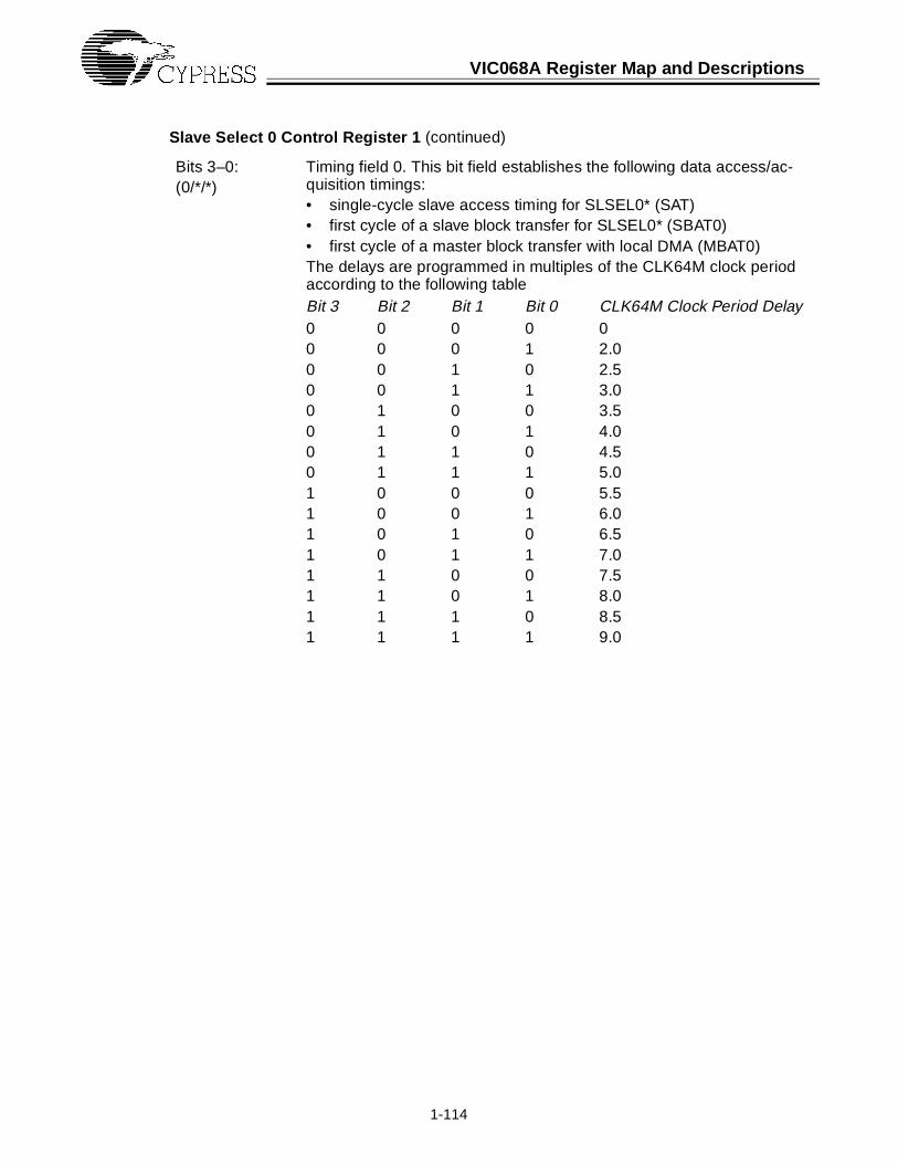
VIC068A Register Map and Descriptions
1-114
Bits 3–0:(0/*/*)
Timing field 0. This bit field establishes the following data access/ac-quisition timings:• single-cycle slave access timing for SLSEL0* (SAT)• first cycle of a slave block transfer for SLSEL0* (SBAT0)• first cycle of a master block transfer with local DMA (MBAT0)The delays are programmed in multiples of the CLK64M clock period according to the following tableBit 3 Bit 2 Bit 1 Bit 0 CLK64M Clock Period Delay0 0 0 0 00 0 0 1 2.00 0 1 0 2.50 0 1 1 3.00 1 0 0 3.50 1 0 1 4.00 1 1 0 4.50 1 1 1 5.01 0 0 0 5.51 0 0 1 6.01 0 1 0 6.51 0 1 1 7.01 1 0 0 7.51 1 0 1 8.01 1 1 0 8.51 1 1 1 9.0
Slave Select 0 Control Register 1 (continued)
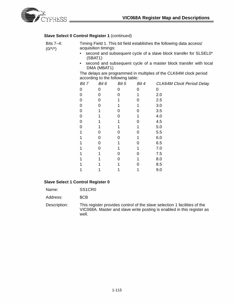
VIC068A Register Map and Descriptions
1-115
Bits 7–4:(0/*/*)
Timing Field 1. This bit field establishes the following data access/acquisition timings:• second and subsequent cycle of a slave block transfer for SLSEL0*
(SBAT1)• second and subsequent cycle of a master block transfer with local
DMA (MBAT1)The delays are programmed in multiples of the CLK64M clock period according to the following table:Bit 7 Bit 6 Bit 5 Bit 4 CLK64M Clock Period Delay0 0 0 0 00 0 0 1 2.00 0 1 0 2.50 0 1 1 3.00 1 0 0 3.50 1 0 1 4.00 1 1 0 4.50 1 1 1 5.01 0 0 0 5.51 0 0 1 6.01 0 1 0 6.51 0 1 1 7.01 1 0 0 7.51 1 0 1 8.01 1 1 0 8.51 1 1 1 9.0
Slave Select 1 Control Register 0
Name: SS1CR0
Address: $CB
Description: This register provides control of the slave selection 1 facilities of the VIC068A. Master and slave write posting is enabled in this register as well.
Slave Select 0 Control Register 1 (continued)

VIC068A Register Map and Descriptions
1-116
Bits 1–0:0/*/*
Local Transfer Mode. These bits set the local transfer mode when the VIC068A is local bus master for both slave and master block transfers.
Bit 1 Bit 0 Mode
0 0 No support is given for slave block transfers onSLSEL1*. The VIC068A will BERR* any attemptto receive a VMEbus block transfer.
0 1 Emulate single-cycle transfers on the local bus.In this mode, the VIC068A emulates single-cycletransfers when performing slave block transfers.By emulating single-cycle transfers, the VIC068Atoggles PAS* for each cycle. DSACKi* must tog-gle for each transfer and not be held asserted.
1 0 Accelerate transfers on the local bus. In thismode, the VIC068A asserts PAS* for the entireslave block transfer. The DSACKi* signals shouldbe held asserted in this mode.
1 1 Undefined/Reserved.
Bits 3–2:(0/*/*)
Address Space Configuration. The SLSEL1* address space is config-ured according to the following table:
Bit 3 Bit 2 Address Space
0 0 A32 (extended)0 1 A24 (standard)1 0 A16 (short)1 1 User defined, uses AMSR
Bit 4:(0/*/*)
D32 enable. D32 slave operations are enabled for SLSEL1* when this bit is set. This bit has no effect for enabling D32 master accesses.
Bit 5:(0/*/*)
Supervisory access. When set, SLSEL1* slave accesses are restricted to supervisory accesses. Other accesses are BERRed. Supervisory accesses are checked with the AM(2) signal.
Bit 6:(0/0/0)
Master write post enable. When set, master write posting is enabled.
Bit 7:(0/0/0)
Slave write post enable. When set, slave write posting is enabled.
Slave Select 1 Control Register 1
Name: SS1CR1
Address: $CF
Description: This register provides the various access and acquisition timings for slave transfers and slave block transfers for SLSEL1*.
Slave Select 1 Control Register 0 (continued)

VIC068A Register Map and Descriptions
1-117
Bits 3–0:(0/*/*)
Timing field 0. This bit field establishes the following data access/ac-quisition timings:• single-cycle slave access timing for SLSEL1* (SAT)• first cycle of a slave block transfer for SLSEL1* (SBAT0)The delays are programmed in multiples of the CLK64M clock period according to the following table:Bit 3 Bit 2 Bit 1 Bit 0 CLK64M Clock Period Delay0 0 0 0 00 0 0 1 2.00 0 1 0 2.50 0 1 1 3.00 1 0 0 3.50 1 0 1 4.00 1 1 0 4.50 1 1 1 5.01 0 0 0 5.51 0 0 1 6.01 0 1 0 6.51 0 1 1 7.01 1 0 0 7.51 1 0 1 8.01 1 1 0 8.51 1 1 1 9.0
Slave Select 1 Control Register 1 (continued)

VIC068A Register Map and Descriptions
1-118
Bits 7–4:(0/*/*)
Timing field 1. This bit field establishes the following data access/ac-quisition timing:• second and subsequent cycle of a slave block transfer for SLSEL1*
(SBAT1)The delays are programmed in multiples of the CLK64M clock period according to the following tables:Bit 7 Bit 6 Bit 5 Bit 4 CLK64M Clock Period Delay0 0 0 0 00 0 0 1 2.00 0 1 0 2.50 0 1 1 3.00 1 0 0 3.50 1 0 1 4.00 1 1 0 4.50 1 1 1 5.01 0 0 0 5.51 0 0 1 6.01 0 1 0 6.51 0 1 1 7.01 1 0 0 7.51 1 0 1 8.01 1 1 0 8.51 1 1 1 9.0
Release Control Register
Name: RCR
Address: $D3
Description: This register configures the VMEbus release mode. The burst count for block transfers with local DMA is also configured in the RCR.
Bits 5-0:(0/0/0)
Block transfer burst length. The burst length for both MOVEM block transfers and block transfers with local DMA are configured in this bit field. The value indicates the number of cycles per block transfer (not the number of bytes). A value of 0 in this bit field indicates the maximum 64 cycles per burst. All other values correspond directly to the burst count.
Bits 7,6:(0/0/0)
Release mode. This bit field defines the release mode used by the VIC068A when releasing the VMEbus after the completion of a VME-bus transfer.
Bit 7 Bit 6 Release Mode
0 0 ROR—Release on Request (default)0 1 RWD—Release When Done1 0 ROC—Release on BCLR* assertion1 1 BCAP—VMEbus Capture and Hold
Slave Select 1 Control Register 1 (continued)

VIC068A Register Map and Descriptions
1-119
Block Transfer Control Register
Name: BTCR
Address: $D7
Description: The BTCR provides control of the VIC068A block transfers. The local interleave periods and data direction are defined in this register. The enabling bits for all of the VIC068A’s block transfer modes are located here as well. These enabling bits are mutually exclusive and more than one should not be set at the same time.
Bits 3–0:(0/0/0)
Interleave period. The interleave period for block transfers is defined here. The interleave period is 250 ns times the value programmed in this bit field.
Bit 4:(0/0/0)
Data direction. This bit defines the direction of a block transfer with local DMA (MOVEM data direction determined by the R/W* signal). When set, VMEbus block reads occur. When clear, VMEbus block writes occur.
Bit 5:(0/0/0)
MOVEM enable. When set, MOVEM transfers are enabled. After this bit is set, the next VMEbus transfer is treated as the start of a VMEbus block transfer. Clearing this bit concludes a MOVEM block transfer in progress. It is important to set this bit immediately before and clear this bit immediately after the actual MOVEM transfer.
Bit 6:(0/0/0)
Block transfer with local DMA enable. When set, block transfers with local DMA are enabled. After this bit is set, the next assertion of MWB* is considered the initiation cycle of a VMEbus block transfer with local DMA. It is important to set this bit immediately before and clear this bit immediately after the actual block transfer.
Bit 7:(0/0/0)
Special purpose. For normal operation set this bit to 0.
Block Transfer Length Registers 1–0
Name: BTLR1–0
Addresses: $DB (BTLR1), $DF (BTLR0)
Description: These registers configure the byte count for block transfers with local DMA. BTLR1 is considered the most significant byte and BTLR0 the least significant. Bit 0 of BTLR0 must never be set because this implies at least one 8-bit transfer is required to complete the block transfer. Only D16 and D32 block transfers are supported. If bit 0 of BTLR0 is set, the block transfer length is ignored and only one burst is performed.
Bits 7–0:(0/0/0)
Block transfer length. Defines the block transfer length in bytes. BTLR1 contains the most significant 8 bits of the length, and BTLR0 the least.

VIC068A Register Map and Descriptions
1-120
System Reset Register
Name: SRR
Address: $E3
Description: The system reset register provides the means to perform a VMEbus system reset (SYSRESET* asserted). Writing a value of $F0 causes this function to occur. A system reset is also performed within the VIC068A.
Bits 7–0:(1/1/1)
System reset field. Writing this bit field with a value of $F0 causes SYSRESET* to be asserted for a minimum of 200 ms and a system reset to be performed within the VIC068A.

1-121
1.13VIC068A AC Performance
SpecificationsClock Input
Note:
1. A 60/40 to 40/60 duty cycle must be maintained.
AC Specifications [2]
Num. Characteristic Min. Max.
Frequency of Operation (MHz) 1 64
1 Cycle Time (ns) 15.6 1000
2, 3 Clock Pulse Width (Measured from 1.5V to 1.5V) Note 1 Note 1
4, 5 Rise and Fall Time (ns) — 5
Operation Notes
Commercial Industrial Military
Min. Max. Min. Max. Min. Max.
ARBITRATION
A1 BRi*[0] to BBSY*[H] 3, 4 2½T+5 3T+25 2½T+4 3T+26 2½T+4 3T+31⁄A2 BRi*[0] to BBSY*[L] 4, 5 3T+8 3½T+28 3T+7 3½T+34 3T+7 3½T+35
A3 BRi*[0] to BGiOUT*[L] 4, 5 3T+4 4T+25 3T+4 4T+26 3T+3 4T+28
A4 BRi*[0] to BCLR*[L] 4 2 16 2 16 2 19
A5 BGiIN*[0] to BGiOUT*[L] 4 2 18 2 18 2 20
A6 BGiIN*[0] to BBSY*[L] 6 4 23 4 24 3 25
A7 BGiIN*[0] to BRi*[H] 4, 6 5 3T+26 4 3T+27 4 3T+31
A8 BGiIN*[1] to BGiOUT*[H] 4 3 20 2 21 2 23
A9 BBSY*[0] to BGiOUT*[H] 4, 5 4 21 3 22 3 24
A10 BBSY*[1] to BGiOUT*[L] 4 3T+5 4T+25 3T+4 4T+26 3T+3 4T+29
A11 BBSY*[1] to BCLR*[H] 4 1T+4 2T+24 1T+4 2T+25 1T+3 2T+27
MASTER ACCESSES
B1 BGiIN*[0] to DENO*[L] 4, 6, 7 8 3T+36 7 3T+37 6 3T+42
B2 BGiIN*[0] to LADO[H] 4, 6 14 3T+59 13 3T+61 12 3T+67
0.8V
2.2V
4 5
1
32

VIC068A AC Performance Specifications
1-122
B3 BGiIN*[0] to AS*[L] 4, 6 3T+5 6T+28 3T+5 6T+29 3T+4 6T+31
B4 BGiIN*[0] to A[7:1] Valid 4, 6 6 3T+31 6 3T+32 5 3T+37
B5 BGiIN*[0] to LWORD*[H/L] 4, 6 6 3T+31 6 3T+32 5 3T+37
B6 BGiIN*[0] to WRITE*[H/L] 4, 6 6 3T+31 6 3T+32 5 3T+37
B7 BGiIN*[0] to ABEN*[L] 4, 6 7 3T+34 6 3T+36 6 3T+38
B8 PAS*[0] & MWB*[0] to BRi*[L]
4 4 22 3 22 3 24
B9 PAS*[0] & MWB*[0] to ISOBE*[L]
4 4 22 3 23 3 25
B10 PAS*[0] & MWB*[0] to LADO[H]
4 15 60 13 62 12 68
B11 PAS*[0] & MWB*[0] to BB-SY*[L]
4, 8 7 32 5 33 5 36
B12 PAS*[0] & MWB*[0] to ABEN*[L]
4, 8 1½T+8 2½T+36 1½T+7 2½T+37 1½T+6 2½T+41
B13 PAS*[0] & MWB*[0] to A[7:1]
4, 8 1½T+7 2½T+36 1½T+6 2½T+37 1½T+5 2½T+41
B14 PAS*[0] & MWB*[0] to LWORD*[H/L]
4, 8 1½T+7 2½T+36 1½T+6 2½T+37 1½T+5 2½T+41
B15 PAS*[0] & MWB*[0] to WRITE*[H/L]
4, 8 1½T+7 2½T+36 1½T+6 2½T+37 1½T+5 2½T+41
B16 PAS*[0] & MWB*[0] & DS*[0] to DS1/0*[L]
4, 8 4½T+10 5½T+46 4½T+9 5½T+47 4½T+9 5½T+57
B17 PAS*[0] & MWB*[0] to SWDEN*[L]
4 7 36 4 12 3 14
B18 PAS*[0] & MWB*[0] to DE-NIN*[L]
4, 9 3 20 3 20 2 22
B19 PAS*[0] & MWB*[0] to DENIN1*[L]
4, 9 3 20 3 21 3 23
B20 PAS*[0] & MWB*[0] & DS*[0] to AS*[L]
4, 8 4½T+6 5½T+28 4½T+5 5½T+29 4½T+5 5½T+32
B21 R/W*[0] to DDIR[H] 4, 7 4 22 3 23 2 25
B22 R/W*[1] to DDIR[L] 4, 7 2 14 1 14 1 15
B23 D[7:0] to LD[7:0] Valid 4, 9 3 18 2 18 2 22
B24 DTACK*[0] to LEDI[H] 4, 9 3T+6 4T+28 3T+4 4T+29 3T+4 4T+32
B25 DTACK*[0] to DSACKi*[L] 4 4 30 3 31 3 36
B26 PAS*[1] & DS*[1] to DSACKi*[H]
4 2 19 2 20 2 27
B27 PAS*[1] to AS*[H] 4 6 30 5 31 5 41
B28 DS*[1] to ISOBE*[H] 4 4 23 3 24 3 26
B29 DS*[1] to SWDEN*[H] 4 4 10 3 10 2 13
B30 DS*[1] to DENIN1*[H] 4, 9 3 19 3 20 2 22
B31 DS*[1] to DENIN*[H] 4, 9 3 19 3 20 2 22
B32 DS*[1] to LD[7:0] Invalid 4, 9 3 20 2 22 2 28
B33 DS*[1] to LD[7:0] Hi-Z 4, 9 3 20 2 22 2 28
B34 DS*[0] to DSACKi*[L] 4, 10 6 T+30 5 T+32 5 T+35
B35 DS*[0] to LADO[H] 4, 10 8 38 7 39 7 43
B36 DS*[0] to LEDO[H] 4, 10 4 T+16 3 T+18 3 T+20
Operation Notes
Commercial Industrial Military
Min. Max. Min. Max. Min. Max.

VIC068A AC Performance Specifications
1-123
LOCAL BUS TIMING (VIC068A AS LOCAL BUS MASTER)
C1 LBG*[0] to PAS*[L] 4 5T+6 6T+31 5T+5 6T+33 5T+5 6T+44
C2 LBG*[0] to LA[7:0] Valid 4 3T+8 4T+36 3T+7 4T+37 3T+6 4T+46
C3 LBG*[0] to SIZ[1:0] Valid 4 1T+3 2T+20 1T+3 2T+21 1T+2 2T+28
C4 LBG*[0] to FC[2:1] Valid 4 1T+3 2T+20 1T+3 2T+21 1T+2 2T+27
C5 LBG*[0] to LD[7:0] Driven 7 3T+8 4T+38 3T+7 4T+39 3T+7 4T+48
C6 LBG*[0] to LAEN[H] 4 3T+10 4T+43 3T+9 4T+44 3T+8 4T+48
C7 LBG*[0] to ISOBE*[L] 4 3T+8 4T+37 3T+7 4T+39 3T+7 4T+42
C8 LBG*[0] to SWDEN*[L] 4 3T+9 4T+39 3T+8 4T+41 3T+7 4T+45
C9 LBG*[0] to DDIR[H] 4, 7 3T+8 4T+37 3T+7 4T+39 3T+7 4T+42
C10 LBG*[0] to DENIN1*[L] 4, 7 3T+7 4T+36 3T+6 4T+38 3T+6 4T+42
C11 LBG*[0] to DENIN*[L] 4, 7 3T+7 4T+32 3T+6 4T+35 3T+5 4T+38
C12 LBG*[0] & DS1/0*[0] & WRITE*[0] to R/W*[L]
4, 7 3T+8 4T+38 3T+7 4T+40 3T+7 4T+47
C13 LBG*[0] & DS1/0*[0] to DS*[L]
4 5T+8 6T+39 5T+7 6T+42 5T+7 6T+56
C14 PAS*[0] to DS*[L] 4, 11 0 12 0 15 0 15
C15 LBR*[H] to LBG*[1] 4, 12 T T T
SLAVE ACCESSES
D1 SLSELi*[0] & AS*[0] to LBR*[L]
4 7 35 6 36 6 40
D2 SLSELi*[0] & AS*[0] & DS1/0*[0] to LADI[H]
4 5 25 4 26 4 29
D3 LD[7:0] to D[7:0] 4, 9 2 16 2 16 2 18
D4 DSACKI*[0] to LEDO[H] 4, 9 SAT+8 SAT+½T+35
SAT+7 SAT+½T+36
SAT+6 SAT+½T+39
D5 DSACKi*[0] to DTACK*[L] 4 SAT+10 SAT+½T+45
SAT+9 SAT+½T+47
SAT+9 SAT+½T+53
D6 DS1/0*[0] to DTACK*[L] 4, 13 2T+5 3½T+28 2T+5 3½T+29 2T+4 3½T+33
D7 DS1/0*[0] to LEDI[H] 4, 13 9 41 8 43 8 47
D8 AS*[1] to LA[7:0], R/W* Invalid
4 5 38 4 42 4 55
D9 AS*[1] to LA[7:0], R/W* High-Z
4 5 38 4 42 4 55
D10 AS*[1] to FC2/1, Invalid 4 10 42 8 44 8 56
D11 AS*[1] & DSACKi*[1] to FC2/1, High-Z
4 10 42 8 44 8 56
D12 AS*[1] to SIZ1/0, Invalid 4 7 32 6 34 6 37
D13 AS*[1] & DSACKi*[1] to SIZ1/0, High-Z
4 3 1T+17 2 1T+19 2 1T+24
D14 AS*[1] to ISOBE*[H] 4 6 30 5 31 5 34
D15 AS*[1] to SWDEN*[H] 4 4 24 4 25 3 27
D16 AS*[1] to DENIN1*[H] 4, 7 5 27 4 28 4 30
D17 AS*[1] to DENIN*[H] 4, 7 5 27 4 28 4 30
D18 AS*[1] & DSACKi*[1] to LBR*[H]
4 5 26 4 27 4 30
Operation Notes
Commercial Industrial Military
Min. Max. Min. Max. Min. Max.

VIC068A AC Performance Specifications
1-124
D19 AS*[1] to LAEN[L] 4 9 40 8 43 7 56
D20 DS*1/0[1] to LD[7:0] Invalid
4, 7 2 27 2 30 2 39
D21 DS*1/0[1] to LD[7:0] High-Z 4, 7 2 27 2 30 2 39
D22 DSACKi*[0] to PAS*[H] 4 SAT+10 SAT+½T+44
SAT+9 SAT+½T+46
SAT+8 SAT+½T+56
D23 DSACKi*[0] to DS*[H] 4 SAT+9 SAT+½T+40
SAT+8 SAT+½T+41
SAT+7 SAT+½T+48
D24 DSi*[1] to DTACK*[H] 4 3 27 3 28 3 35
INTERRUPT
E1 IACKIN*[0] to IACKOUT*[L]
4 2 16 2 17 2 18
E2 IACKIN*[1] to IACKOUT*[H]
4 3 18 2 19 2 20
E3 FCIACK*[0] & PAS*[0] to BRi*[L]
4 5T+9 6T+41 5T+8 6T+42 5T+7 6T+48
E4 FCIACK*[0] & PAS*[0] to IACK*[L]
4, 8 7½T+7 8½T+34 7½T+6 8½T+35 7½T+6 8½T+39
E5 FCIACK*[0] & PAS*[0] to LD[7:0] Driven
4, 14 5T+12 6T+50 5T+10 6T+52 5T+10 6T+57
E6 FCIACK*[0] & PAS*[0] to LD[7:0] valid
4, 15 9T+5 10T+29 9T+5 10T+33 9T+4 10T+37
E7 FCIACK*[0] & PAS*[0] to LIACK0*[L]
4, 16 5T+7 6T+32 5T+6 6T+33 5T+5 6T+36
E8 IRQi*[0] to IPL 4 5 33 5 34 4 37
E9 BGiIN*[0] to BBSY*[L] 4 7 32 5 33 5 36
E10 BGiIN*[0] to AS*[L] 4 3T+5 4T+27 3T+4 4T+28 3T+4 4T+31
E11 BGiIN*[0] to DS1/0*[L] 4 3T+10 4T+45 3T+9 4T+46 3T+8 4T+55
E12 BGiIN*[0] to IACK*[L] 4, 15 39 7 40 7 44
E13 PAS*[0] to ISOBE*[L] 4 5T+9 6T+39 5T+7 6T+40 5T+7 6T+44
E14 PAS*[0] to SWDEN*[L] 4 5T+8 6T+37 5T+7 6T+38 5T+6 6T+42
E15 IPLi to IPLi 4, 11 10 12 12
MASTER BLOCK TRANSFER WITH LOCAL DMA (INITIATION CYCLE)
F1 MWB*[0] & PAS*[0] & DS*[0] to BRi*[L]
4 T+7 2T+32 T+6 2T+33 T+5 2T+38
F2 BGiIN*[0] to LBR*[L] 4 4T+10 5T+42 4T+8 5T+44 4T+8 5T+50
F3 MWB*[0] & PAS*[0] & DS*[0] to LBR*[L]
4, 8 5T+10 6T+42 5T+8 6T+44 5T+8 6T+50
F4 MWB*[0] & PAS*[0] & DS*[0] to LADO[H]
4 T+7 2T+35 T+6 2T+36 T+6 2T+39
F5 MWB*[0] & PAS*[0] & DS*[0] to BLT*[L]
4 T+6 2T+28 T+5 2T+29 T+4 2T+37
MASTER BLOCK TRANSFER WITH LOCAL DMA (WRITE)
** First cycle **
G1 DSACKi*[0] and DS*[0] to DS*[H]
4 MBAT0+9 MBAT0+⁄ T+41
MBAT0+8 MBAT0+½T+43
MBAT0+7 MBAT0+½T+52
Operation Notes
Commercial Industrial Military
Min. Max. Min. Max. Min. Max.

VIC068A AC Performance Specifications
1-125
G2 DSACKi*[0] and DS*[L] to LEDO[H]
4 MBAT0+8 MBAT0+½T+36
MBAT0+7 MBAT0+½T+37
MBAT0+6 MBAT0+½T+40
G3 DSACKi*[0] and DS*[L] to LA[7:0] valid
4 MBAT0+T+11
MBAT0+1½T+32
MBAT0+T+9
MBAT0+1½T+36
MBAT0+T+9
MBAT0+1½T+40
G4 DSACKi*[0] and DS*[L] to DSi*[L]
4 MBAT0+3T+6
MBAT0+3½T+37
MBAT0+3T+5
MBAT0+3½T+39
MBAT0+3T+5
MBAT0+3½T+42
G5 DTACK*[0] to LEDO[L] 4 7 32 6 33 6 38
G6 DTACK*[0] to DSi*[H] 4 10 49 9 51 9 56
G7 DTACK*[0] to A[7:0] Valid 4 11 46 10 48 9 64
G8 DS*[H] to DS*[L] 4 DST+1½T–13 DST+1½T–6
DST+1½T–14 DST–1½T–5
DST+1½T–15 DST+1½T–4
** Second and subsequent cycles **
G9 DSACKi*[0] and DS*[L] to DS*[H]
4 MBAT1+9 MBAT1+½T+41
MBAT1+8 MBAT1+½T+43
MBAT1+7 MBAT1+½T+52
G10 DSACKi*[0] and DS*[L] to LEDO[H]
4 MBAT1+8 MBAT1+½T+36
MBAT1+7 MBAT1+½T+37
MBAT1+6 MBAT1+½T+40
G11 DSACKi*[0] and DS*[L] to LA[7:0] Valid
4 MBAT1+T+11
MBAT1+1½T+32
MBAT1+T+9
MBAT1+1½T+36
MBAT1+T+9
MBAT1+1½T+40
G12 DSACKi*[0] and DS*[L] to DSi*[L]
4 MBAT1+3T+6
MBAT1+3⁄ T+29
MBAT1+3T+5
MBAT1+3⁄ T+30
MBAT1+3T+5
MBAT1+3⁄ T+38
G13 DTACK*[0] to LEDO[L] 4 7 32 6 33 6 38
G14 DTACK*[0] to DSi*[H] 4 10 45 9 46 9 59
G15 DTACK*[0] to A[7:0] Valid 4 11 46 10 48 9 64
G16 DTACK*[0] to DS*[H] 4, 17 T + 15 1⁄ T + 45 1⁄ T + 14 1⁄ T + 46 T + 13 1⁄ T + 47
G17 LEDO[L] to LEDO[H] 4, 17 T + 11 1⁄ T + 25 1⁄ T + 10 1⁄ T + 26 T + 9 1⁄ T + 27
MASTER BLOCK TRANSFER WITH LOCAL DMA (READ)
** First Cycle **
H1 DTACK*[0] to LEDI[H] 2T+6 3T+23 2T+4 3T+25 2T+4 3T+27
H2 DTACK*[0] to DSi*[H] 2T+9 3T+28 2T+8 3T+30 2T+7 3T+32
H3 DTACK*[0] to A[7:0] Valid 4 1½T+10 2½T+44 1½T+9 2½T+45 1½T+8 2½T+53
H4 DTACK*[0] to DS*[L] 4 1½T+8 2½T+38 1½T+7 2½T+40 1½T+7 2½T+47
H5 DSACKi*[0] and DS*[L] to DS*[H]
MBAT0+9 MBAT0+½T+38
MBAT0+8 MBAT0+½T+40
MBAT0+7 MBAT0+½T+45
H6 DSACKi*[0] and DS*[L] to LEDI[L]
MBAT0+9 MBAT0+½T+48
MBAT0+8 MBAT0+½T+50
MBAT0+7 MBAT0+½T+55
H7 DSACKi*[0] and DS*[L] to LA[7:0] Valid
4 MBAT0+T+11
MBAT0+1½T+30
MBAT0+T+9
MBAT0+1½T+32
MBAT0+T+9
MBAT0+1½T+35
H8 DSACKi*[0] and DS*[L] to DSi*[L]
4 MBAT0+11 MBAT0+½T+74
MBAT0+10 MBAT0+½T+76
MBAT0+10 MBAT0+½T+83
** Second and subsequent cycles **
H9 DTACK*[0] to LEDI[H] 4 2T+6 3T+23 2T+4 3T+25 2T+4 3T+27
H10 DTACK*[0] to DSi*[H] 4 2T+9 3T+28 2T+8 3T+30 2T+7 3T+32
H11 DTACK*[0] to A[7:0] Valid 4 10 44 9 45 8 53
H12 DTACK*[0] to DS*[L] 4 8 38 7 40 7 47
H13 DSACKi*[0] and DS*[0] to DS*[H]
4 MBAT1+9 MBAT1+½T+36
MBAT1+8 MBAT1+½T+38
MBAT1+7 MBAT1+½T+45
Operation Notes
Commercial Industrial Military
Min. Max. Min. Max. Min. Max.

VIC068A AC Performance Specifications
1-126
H14 DSACKi*[0] and DS*[0] to LEDI[L]
4 MBAT1+9 MBAT1+½T+44
MBAT1+8 MBAT1+½T+46
MBAT1+7 MBAT1+½T+55
H15 DSACKi*[0] and DS*[0] to LA[7:0] Valid
4 MBAT1+T+11
MBAT1+1½T+31
MBAT1+T+9
MBAT1+1½T+33
MBAT1+T+9
MBAT1+1½T+35
H16 DSACKi*[0] and DS*[0] to DSi*[L]
4 MBAT1+11 MBAT1+½T+72
MBAT1+10 MBAT1+½T+76
MBAT1+10 MBAT1+½T+83
MASTER BLOCK TRANSFER WITH LOCAL DMA (BOUNDARY CROSSING)
J1 DS*[L] to BLT*[H] 2 30 2 32 2 35
J2 DS*[H] to BLT*[L] 2 17 2 19 2 21
J3 DSi*[L] to LEDO[H/L] 2 21 2 23 2 25
J4 DSi*[H] to LADO[L/H] 4 1 16 2 18 2 20
SLAVE BLOCK TRANSFER (WRITE)
** First Cycle **
See: Local Bus Timing (VIC068A as local bus master)
** Second and subsequent cycles **
K1 DSi*[0] to LEDI[H] 4 4 20 4 22 4 24
K2 DSi*[0] to DS*[L] 6 35 5 36 5 39
K3 DSACKi*[0] and DS*[L] to DS*[H]
4 SBAT+9 SBAT+½T+41 SBAT+8 SBAT+½T+42 SBAT+7 SBAT+½T+52
K4 DSACKi*[0] and DS*[L] to DTACK*[L]
4 SBAT+12 SBAT+½T+51 SBAT+11 SBAT+½T+53 SBAT+10 SBAT+½T+67
K5 DSACKi*[0] and DS*[L] to ISOBE*[H]
4 SBAT+13 SBAT+½T+54 SBAT+11 SBAT+½T+56 SBAT+11 SBAT+½T+62
K6 DSACKi*[0] and DS*[L] to SWDEN*[H]
4 SBAT+12 SBAT+½T+50 SBAT+10 SBAT+½T+52 SBAT+10 SBAT+½T+61
K7 DSACKi*[0] and DS*[L] to LA[7:0] Invalid
4 SBAT+T+10
SBAT+1½T+34
SBAT+T+8 SBAT+1½T+36
SBAT+T+8 SBAT+1½T+40
K8 DSACKi*[0] and DS*[L] to LEDI*[L]
4 SBAT+8 SBAT+½T+46
SBAT+7 SBAT+½T+48
SBAT+6 SBAT+½T+53
K9 DS1/0*[1] to DTACK*[H] 4 5 27 5 28 4 35
SLAVE BLOCK TRANSFER (READ)
** First Cycle **
See: Local Bus Timing (VIC068A as local bus master)
** Second and subsequent cycles **
L1 DS1/0*[1] to LEDO[L] 4 23 3 24 3 30
L2 DS*[H] to DS*[L] 4 DST+1½T–13
DST+1½T–2
DST+1½T–14
DST+1½T–3
DST+1½T–15
DST+1½T–4
L3 DS1/0*[0] to DENO*[L] 4 3 20 3 22 3 24
L4 DSACKi*[0] and DS*[0] to LEDO[H]
4 SBAT+8 SBAT+½T+36 SBAT+7 SBAT+½T+37 SBAT+6 SBAT+½T+41
L5 DSACKi*[0] and DS*[0] to DS*[H]
4 SBAT+9 SBAT+½T+41 SBAT+8 SBAT+½T+43 SBAT+7 SBAT+½T+52
L6 DSACKi*[0] and DS*[0] to DTACK*[L]
SBAT+11 SBAT+½T+47 SBAT+9 SBAT+½T+48 SBAT+9 SBAT+½T+53
L7 DSACKi*[0] and DS*[0] to LA[7:0] Invalid
4 SBAT+T+9 SBAT+1½T+34
SBAT+T+8 SBAT+1½T+36
SBAT+T+8 SBAT+½T+40
L8 DS1/0*[1] to DENO*[H] 4 3 19 3 20 2 22
Operation Notes
Commercial Industrial Military
Min. Max. Min. Max. Min. Max.

VIC068A AC Performance Specifications
1-127
Notes:
L9 DS1/0*[1] to DTACK*[H] 4 3 20 3 21 3 24
L10 LEDO[L] to LEDO[H] 4, 18 T + 11 1½ + 25 T + 10 1½ + 26 1½ + 9 1½ + 27
L11 DTACK*[0] to DS*[H] 4, 18 T + 15 1½ + 45 1½ + 14 1½ + 46 1½ + 13 1½ + 47
REGISTER ACCESS
M1 PAS*[0] & DS*[0] & CS*[0] to DSACKi*[L]
4 4T+5 5T+34 4T+5 5T+35 4T+4 5T+38
M2 PAS*[0] & DS*[0] & CS*[0] to LD[7:0] Valid
4, 9 3T+5 4T+28 3T+5 4T+29 3T+4 4T+37
M3 AS*[0] & ICFSEL*[0] to DTACK*[L]
4 4T+6 4T+30 4T+5 4T+31 4T+5 4T+34
RESET
N1 LBG*[0] to HALT*[L], RE-SET*[L]
4 8 36 7 37 6 48
N2 IRESET*[0] to LBR*[L] 4 6 29 5 30 5 33
N3 IRESET*[0] to IPL0[Z] 4 2 16 2 16 2 20
SET-UP TIMES
P1 LA, ASIZ[1:0] Valid to PAS*[0]
4 –2T –2T –2T
P2 SIZ[1:0], WORD*, FC[2:1] Valid to PAS*[0]
4 –2T –2T –2T
P3 LD[7:0] Valid to DS*[0] 4 0 0 0
HOLD TIMES
Q1 PAS*[1] to LA, ASIZ[1:0] In-valid
4 0 0 0
Q2 PAS*[1] to SIZ[1:0], WORD*, FC[2:1] Invalid
4 0 0 0
Q3 DS*[1] to LD[7:0] Invalid 4 0 0 0
Q4 DS1/0*[1] to DTACK*[H] 4 0 0 0
2. T = CLK64M clock periodSAT = Slave Access TimingMBAT0 = Master Block Transfer Timing 0MBAT1 = Master Block Transfer Timing 1SBAT = Slave Block Transfer TimingDST = Data Strobe Timing
3. ROR mode.
4. Timing specified but not tested.
5. While VMEbus system controller.
6. Synchronous delay depends on speed in whichBGiIN* is returned. If BGiIN* is returned in zero timeafter request, synchronous delay will be maximum.
7. Write operation only.
8. While VMEbus master.
9. Read operation only.
10. Master write post only.
11. Skew.
12. Input requirement.
13. Slave write post only.
14. VMEbus interrupt only.
15. Local interrupt (LICR[4] = 1) only.
16. Local interrupt (LICR[4] = 0) only.
17. “Slow” Slave.
18. “Slow” Master.
Operation Notes
Commercial Industrial Military
Min. Max. Min. Max. Min. Max.

VIC068A AC Performance Specifications
1-128
Figure 1-21. VMEbus Arbitration—VIC068A as Arbitor, priority interrupt
Figure 1-22. VMEbus Arbitration—VIC068A as System Controller (granting bus internally)
Figure 1-23. VMEbus Arbitration—VIC068A (not System Controller) Honoring ROR
OUTPUT
INPUT
BRi*
BGiOUT*
BBSY*
BCLR*
INPUT
OUTPUT
A11A4
A10
A9 A3
OUTPUTBRi*
BGiOUT*
BBSY*
A2
OUTPUT
OUTPUT
OUTPUT
INPUT
BRi*
BGiOUT*
BBSY*
BGiIN*
INPUT
OUTPUT
A1 A5 A8

VIC068A AC Performance Specifications
1-129
Figure 1-24. VMEbus Arbitration—VIC068A (not System Controller) Taking the VMEbus
OUTPUT
BRi*
BBSY*
BGiIN* INPUT
A6
OUTPUT
A7

VIC068A AC Performance Specifications
1-130
Figure 1-25. Master Write
OUTPUT
PAS*
DS*
INPUT
P1P3
B26
Q3
B29
B28
Q1B25B10
B9
B22
B17
B21
B2B1
B8B3
B27
B5
B4
B6
INPUT
INPUT
INPUT
INPUT
INPUT
OUTPUT
OUTPUT
OUTPUT
OUTPUT
OUTPUT
OUTPUT
OUTPUT
OUTPUT
OUTPUT
OUTPUT
OUTPUT
OUTPUT
OUTPUT
OUTPUT
OUTPUT
INPUT
INPUT
MWB*
DSACKi*
R/W*
LA[7:0]
LD[7:0]
LEDO
DENO*
LADO
ABEN*
ISOBE*
SWDEN*
DDIR
BRi*
BGiIN*
AS*
DS1/0*
LWORD*
WRITE*
BBSY*
DTACK*
A[7:1]
D[7:0]
VALID
VALID
VALID
VALID

VIC068A AC Performance Specifications
1-131
Figure 1-26. Master Read
OUTPUT
PAS*
DS*
INPUT
B5
B4
B6
INPUT
INPUT
INPUT
INPUT
OUTPUT
OUTPUT
OUTPUT
OUTPUT
OUTPUT
OUTPUT
OUTPUT
OUTPUT
OUTPUT
OUTPUT
OUTPUT
OUTPUT
OUTPUT
OUTPUT
OUTPUT
INPUT
INPUT
INPUT
MWB*
DSACKi*
R/W*
LA[7:0]
LD[7:0]
LEDI
DENIN/1*
LADO
ABEN*
ISOBE*
SWDEN*
DDIR
BRi*
BGiIN*
AS*
DS1/0*
LWORD*
WRITE*
BBSY*
DTACK*
A[7:1]
D[7:0]
P1P3
B26
Q3
B28
Q1B25
B10
B18,B19
B7 B23
B24B32
B33
B30, B31
B3B27
B17B9
B2
B8
B29
VALID
VALID
VALID
VALID

VIC068A AC Performance Specifications
1-132
Figure 1-27. Slave Write
INPUT
PAS*
DS*
INPUT
OUTPUT
OUTPUT
OUTPUT
OUTPUT
OUTPUT
OUTPUT
OUTPUT
OUTPUT
OUTPUT
OUTPUT
OUTPUT
OUTPUT
OUTPUT
OUTPUT
INPUT
INPUT
INPUT
INPUT
INPUT
INPUT
OUTPUT
OUTPUT
SLSELi*
DSACKi*
R/W*
LA[7:0]
FCi
SIZi
LD[7:0]
LEDI
DENIN/1*
LADI
LAEN
ISOBE*
SWDEN*
DDIR
LBR*
LBG*
AS*
DS1/0*
WRITE*
DTACK*
A[7:1]
D[7:0]
D22
D23
D2
D1
D8
D9D10
D12 D11
D13D21D20
D16, D17
D19
D15D14
D18
D5
D24
VALID
VALID
VALID
VALID
VALID
VALID

VIC068A AC Performance Specifications
1-133
Figure 1-28. Slave Read
INPUT
PAS*
DS*
INPUT
OUTPUT
OUTPUT
OUTPUT
OUTPUT
OUTPUT
OUTPUT
INPUT
OUTPUT
OUTPUT
OUTPUT
OUTPUT
OUTPUT
OUTPUT
OUTPUT
INPUT
INPUT
INPUT
INPUT
INPUT
OUTPUT
OUTPUT
OUTPUT
SLSELi*
DSACKi*
R/W*
LA[7:0]
FCi
SIZi
LD[7:0]
LEDO
DENO*
LADI
LAEN
ISOBE*
SWDEN*
DDIR
LBR*
LBG*
AS*
DS1/0*
WRITE*
DTACK*
A[7:1]
D[7:0]
D2
D1
D8
D9D10
D12 D11
D13
D4
D3
D16, D17
D19
D15D14
D18
D5D24
D22
D23
VALID
VALID
VALID
VALID
VALID
VALID

VIC068A AC Performance Specifications
1-134
Figure 1-29. Master Write Post
OUTPUT
PAS*
DS*
INPUT
P1P3
B26
Q3
B29B28
Q1
B9B17
B21
B2B1
B8B3
B5
B4
B6
INPUT
INPUT
INPUT
INPUT
INPUT
OUTPUT
OUTPUT
OUTPUT
OUTPUT
OUTPUT
OUTPUT
OUTPUT
OUTPUT
OUTPUT
OUTPUT
OUTPUT
OUTPUT
OUTPUT
OUTPUT
OUTPUT
INPUT
INPUT
MWB*
DSACKi*
R/W*
LA[7:0]
LD[7:0]
LEDO
DENO*
LADO
ABEN*
ISOBE*
SWDEN*
DDIR
BRi*
BGiIN*
AS*
DS1/0*
LWORD*
WRITE*
BBSY*
DTACK*
A[7:1]
D[7:0]
B36
B35
B34
B10
B7
VALID
VALID
VALID
VALID

VIC068A AC Performance Specifications
1-135
Figure 1-30. Slave Write Post
INPUT
PAS*
DS*
INPUT
OUTPUT
OUTPUT
OUTPUT
OUTPUT
OUTPUT
OUTPUT
OUTPUT
OUTPUT
OUTPUT
OUTPUT
OUTPUT
OUTPUT
OUTPUT
OUTPUT
INPUT
INPUT
INPUT
INPUT
INPUT
INPUT
OUTPUT
OUTPUT
SLSELi*
DSACKi*
R/W*
LA[7:0]
FCi
SIZi
LD[7:0]
LEDI
DENIN/1*
LADI
LAEN
ISOBE*
SWDEN*
DDIR
LBR*
LBG*
AS*
DS1/0*
WRITE*
DTACK*
A[7:1]
D[7:0]
D22
D23
D2
D1
D8
D9D10
D12 D11
D13
D16, D17
D15D14
D6
D7
VALID
VALID
VALID
VALID
VALID
VALID

VIC068A AC Performance Specifications
1-136
Figure 1-31. Local Bus
INPUT
PAS*
DS* OUTPUT
OUTPUT
OUTPUT
OUTPUT
OUTPUT
OUTPUT
OUTPUT
OUTPUT
OUTPUT
OUTPUT
OUTPUT
OUTPUT
OUTPUT
OUTPUT
INPUT
OUTPUT
DSACKi*
R/W*
LA[7:0]
FCi
SIZi
LD[7:0]
DENIN*
LADI
LAEN
ISOBE*
SWDEN*
DDIR
LBR*
LBG*
C7
DENIN1*
C8
C9
C6
C11
C10
C5
C3
C4
C2
C12
C14
C13
C1
C15

VIC068A AC Performance Specifications
1-137
Figure 1-32. While VME Master
PAS*
DS*
INPUT
INPUT
INPUT
OUTPUT
OUTPUT
OUTPUT
OUTPUT
OUTPUT
OUTPUT
MWB*
AS*
DS1/0*
LWORD*
WRITE*
A[7:1]
B13
ABEN*
B15
B14
B16
B20
B12

VIC068A AC Performance Specifications
1-138
Figure 1-33. VME IACK
OUTPUT
PAS*
FCIACK*
E1
INPUT
INPUT
OUTPUT
INPUT
OUTPUT
OUTPUT
OUTPUT
OUTPUT
OUTPUT
OUTPUT
INPUT
OUTPUT
OUTPUT
INPUT
OUTPUT
OUTPUT
DSACKi*
IPLi
IRQi*
LD[7:0]
LIACKO*
ISOBE*
SWDEN*
BRi*
BGiIN*
AS*
DS1/0*
LWORD*
IACK*
BBSY*
DTACK*
D[7:0]
INPUT
OUTPUT
IACKIN*
IACKOUT*
E2
E9
E12
E11
E10
E13
E6
E4
E5E8
E15 E3
E14
INPUT
VALID
VALID
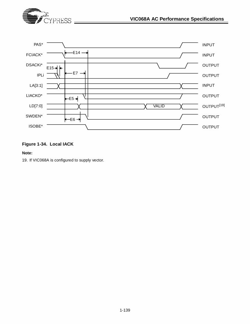
VIC068A AC Performance Specifications
1-139
Figure 1-34. Local IACK
Note:
19. If VIC068A is configured to supply vector.
PAS*
FCIACK*
DSACKi*
IPLi
LD[7:0]
LIACKO*
ISOBE*
SWDEN*E6
E5
E15E7
E14
LA[3:1]
OUTPUT[19]VALID
OUTPUT
OUTPUT
OUTPUT
OUTPUT
OUTPUT
INPUT
INPUT
INPUT

VIC068A AC Performance Specifications
1-140
Figure 1-35. Initiation
OUTPUT
PAS*
DS*
INPUT
INPUT
INPUT
INPUT
INPUT
INPUT
OUTPUT
OUTPUT
OUTPUT
OUTPUT
INPUT
MWB*
DSACKi*
R/W*
LA[31:0]
LD[31:0]
LADO
LBR*
BRi*
BGiIN*
BLT*
Initiation
F2
F4
F3
F5
F1
VALID
VALID

VIC068A AC Performance Specifications
1-141
Figure 1-36. First MBLT Write
INPUT
PAS*
DS*
G4
OUTPUT
OUTPUT
OUTPUT
OUTPUT
OUTPUT
OUTPUT
OUTPUT
OUTPUT
OUTPUT
OUTPUT
INPUT
INPUT
DSACKi*
R/W*
LA[31:0]
LD[31:0]
LEDO
LBG*
AS*
DSi*
DTACK*
A[7:1]
D[+:0]
G2
G3
G1
G5G6G7
G8
VALID
VALID
VALID
VALID
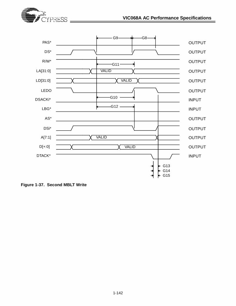
VIC068A AC Performance Specifications
1-142
Figure 1-37. Second MBLT Write
INPUT
PAS*
DS*
G12
OUTPUT
OUTPUT
OUTPUT
OUTPUT
OUTPUT
OUTPUT
OUTPUT
OUTPUT
OUTPUT
OUTPUT
INPUT
INPUT
DSACKi*
R/W*
LA[31:0]
LD[31:0]
LEDO
LBG*
AS*
DSi*
DTACK*
A[7:1]
D[+:0]
G10
G11
G9
G13G14G15
G8
VALID
VALID
VALID
VALID

VIC068A AC Performance Specifications
1-143
Figure 1-38. Master Block Transfer—Write (Slow Slave)
PAS*
DS*
DTACK*
LA[31:0]
LD[31:0]
R/W*
DSACKi*
LEDO
AS*
DSi*
A[+:1]
D[+:0]
Local Bus Signals
VMEbus Signals
LBG*
MBAT0
G8
G17
G16

VIC068A AC Performance Specifications
1-144
Figure 1-39. First MBLT Read
INPUT
PAS*
DS*
H8
OUTPUT
OUTPUT
OUTPUT
OUTPUT
OUTPUT
OUTPUT
OUTPUT
OUTPUT
OUTPUT
INPUT
INPUT
INPUT
DSACKi*
R/W*
LA[31:0]
LD[31:0]
LEDI
LBG*
AS*
DSi*
DTACK*
A[7:1]
D[+:0]
H6
H7
H5
H1H2H3H4
VALID
VALID
VALID
VALID

VIC068A AC Performance Specifications
1-145
Figure 1-40. Second MBLT Read
INPUT
PAS*
DS* OUTPUT
OUTPUT
OUTPUT
OUTPUT
OUTPUT
OUTPUT
OUTPUT
OUTPUT
OUTPUT
INPUT
INPUT
INPUT
DSACKi*
R/W*
LA[31:0]
LD[31:0]
LEDI
LBG*
AS*
DSi*
DTACK*
A[7:1]
D[+:0]
H16
H14
H15
H13
H9H10H11H12
H9H10H11H12
H16
H14
H15
H13
VALID VALID
VALID VALID VALID
VALID VALID

VIC068A AC Performance Specifications
1-146
Figure 1-41. Boundary Crossing
J2
J3
J4
J1
BLT*
Local Boundary Crossing
DS*
LADO
VMEbus Boundary Crossing
DSi*

VIC068A AC Performance Specifications
1-147
Figure 1-42. Slave Write BLT
INPUT
PAS*
DS*
INPUT
K2
OUTPUT
OUTPUT
OUTPUT
OUTPUT
OUTPUT
OUTPUT
OUTPUT
INPUT
OUTPUT
OUTPUT
INPUT
INPUT
INPUT
INPUT
OUTPUT
SLSELi*
DSACKi*
R/W*
LA[31:0]
LD[31:0]
LEDI
LBR*
LBG*
ISOBE*
SWDEN*
AS*
DSi*
DTACK*
A[+:1]
D[+:0]
K3
K7
K5
K6
K4
K1
K9
VALID
VALID
K8

VIC068A AC Performance Specifications
1-148
Figure 1-43. Slave Read BLT
INPUT
PAS*
DS*
INPUT
OUTPUT
OUTPUT
OUTPUT
OUTPUT
INPUT
OUTPUT
OUTPUT
INPUT
OUTPUT
INPUT
INPUT
INPUT
OUTPUT
OUTPUT
SLSELi*
DSACKi*
R/W*
LA[31:0]
LD[31:0]
LEDO
LBR*
LBG*
DENO*
AS*
DSi*
DTACK*
A[+:1]
D[+:0]
L7
L3
L4
L6
L1
L8
L5
L9

VIC068A AC Performance Specifications
1-149
Figure 1-44. Slave Block Tran sfer—Read, Slow Master
PAS*
DS*
DTACK*
LA[31:0]
LD[31:0]
R/W*
DSACKi*
LEDO
AS*
DSi*
A[+:1]
D[+:0]
Local Bus Signals
VMEbus Signals
LBG*
SLSEL1*
LBR*
L2
L10
L11
L4

VIC068A AC Performance Specifications
1-150
Figure 1-45. Register Operations
PAS*
DS* INPUT
INPUT
INPUT
INPUT
OUTPUT
INPUT
CS*
R/W*
DSACK1/0*
D[7:0]
Write
M1
Read
PAS*
DS* INPUT
INPUT
INPUT
INPUT
OUTPUT
OUTPUT
CS*
R/W*
DSACK1/0*
D[7:0]
ICF Select
INPUT
INPUT
OUTPUT
AS*
ICFSEL*
DTACK*
M1
M2
M3
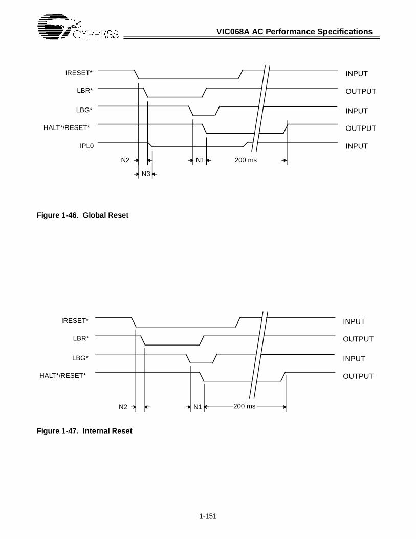
VIC068A AC Performance Specifications
1-151
Figure 1-46. Global Reset
Figure 1-47. Internal Reset
N1
N3
OUTPUT
INPUT
OUTPUT
INPUT
INPUT
HALT*/RESET*
IRESET*
LBR*
LBG*
IPL0
N2 200 ms
N1N2 200 ms
OUTPUT
INPUT
OUTPUT
INPUT
HALT*/RESET*
IRESET*
LBR*
LBG*

1-152
1.14VIC068A Signal List and
PinoutsTable 1-17. VMEbus Signals
NamePGAPin
QFPPin Type Description
D07 H15 99 Three-State I/O VMEbus Data
D06 H14 98 Three-State I/O VMEbus Data
D05 J15 97 Three-State I/O VMEbus Data
D04 K15 96 Three-State I/O VMEbus Data
D03 J14 94 Three-State I/O VMEbus Data
D02 L15 93 Three-State I/O VMEbus Data
D01 K14 92 Three-State I/O VMEbus Data
D00 K13 91 Three-State I/O VMEbus Data
A07 N2 33 Three-State I/O VMEbus Address
A06 L3 32 Three-State I/O VMEbus Address
A05 M2 31 Three-State I/O VMEbus Address
A04 M1 29 Three-State I/O VMEbus Address
A03 L2 28 Three-State I/O VMEbus Address
A02 L1 27 Three-State I/O VMEbus Address
A01 K2 25 Three-State I/O VMEbus Address
AM5 R10 63 Three-State I/O VMEbus Address Modifier
AM4 R9 62 Three-State I/O VMEbus Address Modifier
AM3 R8 59 Three-State I/O VMEbus Address Modifier
AM2 P8 58 Three-State I/O VMEbus Address Modifier
AM1 R7 57 Three-State I/O VMEbus Address Modifier
AM0 R6 56 Three-State I/O VMEbus Address Modifier
BG3IN* N14 84 Input VMEbus Bus Grant Input
BG3OUT* M15 90 Output VMEbus Bus Grant Output
BG2IN* M13 83 Input VMEbus Bus Grant Input
BG2OUT* N15 88 Output VMEbus Bus Grant Output
BG1IN* P14 77 Input VMEbus Bus Grant Input
BG1OUT* L13 87 Output VMEbus Bus Grant Output
BG0IN* N13 76 Input VMEbus Bus Grant Input
BG0OUT* M14 86 Output VMEbus Bus Grant Output

VIC068A Signal List and Pinouts
1-153
BR3* P13 73 Open Collector I/O VMEbus Request
BR2* N11 72 Open Collector I/O VMEbus Request
BR1* P12 71 Open Collector I/O VMEbus Request
BR0* R12 69 Open Collector I/O VMEbus Request
IACK* P6 52 Rescinding Three-State I/O VMEbus Interrupt Acknowledge
IACKIN* N6 51 Input VMEbus Interrupt Acknowledge Input
IACKOUT* R4 50 Output VMEbus Interrupt Acknowledge Output
IRQ7* R2 45 Open Collector I/O VMEbus Interrupt Request
IRQ6* P3 44 Open Collector I/O VMEbus Interrupt Request
IRQ5* N4 43 Open Collector I/O VMEbus Interrupt Request
IRQ4* R1 38 Open Collector I/O VMEbus Interrupt Request
IRQ3* P2 37 Open Collector I/O VMEbus Interrupt Request
IRQ2* N3 36 Open Collector I/O VMEbus Interrupt Request
IRQ1* M3 35 Open Collector I/O VMEbus Interrupt Request
BBSY* N12 75 Rescinding Three-State I/O VMEbus Busy
BCLR* R14 74 Three-State I/O VMEbus Clear
AS* P7 54 Rescinding Three-State I/O VMEbus Address Strobe
DS1* P11 68 Rescinding Three-State I/O VMEbus DataStrobe
DS0* R11 67 Rescinding Three-State I/O VMEbus Data Strobe
DTACK* R5 53 Rescinding Three-State I/O VMEbus Data Transfer Acknowledge
BERR* N10 66 Rescinding Three-State I/O VMEbus Error
LWORD* P9 64 Rescinding Three-State I/O VMEbus Long-Word
WRITE* P10 65 Rescinding Three-State I/O VMEbus Data Direction
SYSCLK* P15 85 Three-State Output VMEbus Syatem Clock
SYSRESET* P5 49 Open Collector I/O VMEbus System Reset
ACFAIL* R3 48 Input VMEbus AC Fail
SYSFAIL* N5 47 Open Collector I/O VMEbus System Fail
Table 1-17. VMEbus Signals (continued)
NamePGAPin
QFPPin Type Description
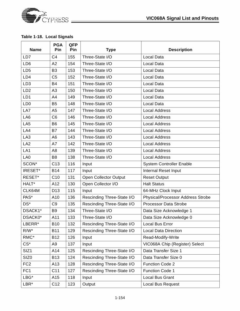
VIC068A Signal List and Pinouts
1-154
Table 1-18. Local Signals
NamePGA Pin
QFP Pin Type Description
LD7 C4 155 Three-State I/O Local Data
LD6 A2 154 Three-State I/O Local Data
LD5 B3 153 Three-State I/O Local Data
LD4 C5 152 Three-State I/O Local Data
LD3 B4 151 Three-State I/O Local Data
LD2 A3 150 Three-State I/O Local Data
LD1 A4 149 Three-State I/O Local Data
LD0 B5 148 Three-State I/O Local Data
LA7 A5 147 Three-State I/O Local Address
LA6 C6 146 Three-State I/O Local Address
LA5 B6 145 Three-State I/O Local Address
LA4 B7 144 Three-State I/O Local Address
LA3 A6 143 Three-State I/O Local Address
LA2 A7 142 Three-State I/O Local Address
LA1 A8 139 Three-State I/O Local Address
LA0 B8 138 Three-State I/O Local Address
SCON* C13 116 Input System Controller Enable
IRESET* B14 117 Input Internal Reset Input
RESET* C10 131 Open Collector Output Reset Output
HALT* A12 130 Open Collector I/O Halt Status
CLK64M D13 115 Input 64-MHz Clock Input
PAS* A10 136 Rescinding Three-State I/O Physical/Processor Address Strobe
DS* C9 135 Rescinding Three-State I/O Processor Data Strobe
DSACK1* B9 134 Three-State I/O Data Size Acknowledge 1
DSACK0* A11 133 Three-State I/O Data Size Acknowledge 0
LBERR* B10 132 Rescinding Three-State I/O Local Bus Error
R/W* B11 129 Rescinding Three-State I/O Local Data Direction
RMC* B12 126 Input Read-Modify-Write
CS* A9 137 Input VIC068A Chip (Register) Select
SIZ1 A14 125 Rescinding Three-State I/O Data Transfer Size 1
SIZ0 B13 124 Rescinding Three-State I/O Data Transfer Size 0
FC2 A13 128 Rescinding Three-State I/O Function Code 2
FC1 C11 127 Rescinding Three-State I/O Function Code 1
LBG* A15 118 Input Local Bus Grant
LBR* C12 123 Output Local Bus Request

VIC068A Signal List and Pinouts
1-155
IPL2 B1 5 Output Interrupt Priority Level 2
IPL1 C2 4 Output Interrupt Priority Level 1
IPL0 D3 3 Three-State I/O Interrupt Priority Level 0/Global Reset
BLT* B2 157 Open Collector I/O Block Transfer Status
DEDLK* C3 156 Output Deadlock Status
LIACKO* C1 8 Output Local Interrupt Autovector
LIRQ7* G3 15 Input Local Interrupt Request 7
LIRQ6* G2 14 Input Local Interrupt Request 6
LIRQ5* E1 13 Input Local Interrupt Request 5
LIRQ4* F2 12 Input Local Interrupt Request 4
LIRQ3* F3 11 Input Local Interrupt Request 3
LIRQ2* D1 10 Three-State I/O (w/PU) Local Interrupt Request 2
LIRQ1* E2 9 Input Local Interrupt Request 1
MWB* J2 24 Input Module Wants Bus
FCIACK* K1 23 Input Interrupt Acknowledge
WORD* J1 22 Input D16/D32 Control
SLSEL1* H1 19 Input Slave Select 1
SLSEL0* J3 21 Input Slave Select 0
ICFSEL* H2 18 Input ICF Select
ASIZ1 F1 16 Input Address Size 1
ASIZ0 G1 17 Input Address Size 0
Table 1-18. Local Signals (continued)
NamePGA Pin
QFP Pin Type Description

VIC068A Signal List and Pinouts
1-156
Table 1-19. Buffer Control Signals
NamePGA Pin
QFP Pin Type Description
ABEN* B15 114 Output VMEbus Address Buffer Enable
LADO C14 113 Output Latch Outgoing VMEbus Address
LADI E13 112 Output Latch Incomming VMEbus Address
LEDO D15 109 Output Latch Outgoing VMEbus Data
LEDI D14 111 Output Latch Incomming VMEbus Data
DDIR E14 108 Output Local Data Direction
DENIN1* E15 107 Output Local Data Enable In (Upper Word)
DENIN* F14 105 Output Local Data Enable In (Lower Word)
SWDEN* F15 103 Output Swap Local Data Enable
DENO* G14 104 Output VMEbus Data Buffer Enable
ISOBE* G15 102 Output Isolation Buffer Enable
LAEN E3 7 Output Local Address Buffer Enable
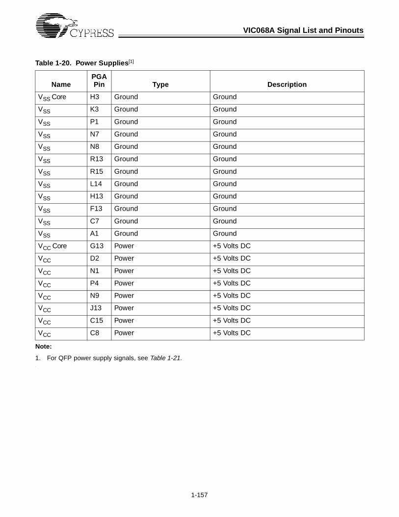
VIC068A Signal List and Pinouts
1-157
Note:
1. For QFP power supply signals, see Table 1-21..
Table 1-20. Power Supplies [1]
NamePGA Pin Type Description
VSS Core H3 Ground Ground
VSS K3 Ground Ground
VSS P1 Ground Ground
VSS N7 Ground Ground
VSS N8 Ground Ground
VSS R13 Ground Ground
VSS R15 Ground Ground
VSS L14 Ground Ground
VSS H13 Ground Ground
VSS F13 Ground Ground
VSS C7 Ground Ground
VSS A1 Ground Ground
VCC Core G13 Power +5 Volts DC
VCC D2 Power +5 Volts DC
VCC N1 Power +5 Volts DC
VCC P4 Power +5 Volts DC
VCC N9 Power +5 Volts DC
VCC J13 Power +5 Volts DC
VCC C15 Power +5 Volts DC
VCC C8 Power +5 Volts DC
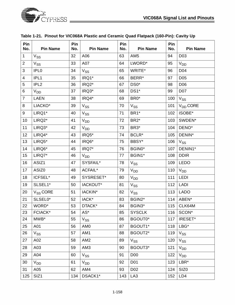
VIC068A Signal List and Pinouts
1-158
Table 1-21. Pinout for VIC068A Plastic and Ceramic Quad Flatp ack (160-Pin): Cavity Up
Pin No. Pin Name
Pin No. Pin Name
Pin No. Pin Name
Pin No. Pin Name
1 VSS 32 A06 63 AM5 94 D03
2 VSS 33 A07 64 LWORD* 95 VDD
3 IPL0 34 VSS 65 WRITE* 96 D04
4 IPL1 35 IRQ1* 66 BERR* 97 D05
5 IPL2 36 IRQ2* 67 DS0* 98 D06
6 VDD 37 IRQ3* 68 DS1* 99 D07
7 LAEN 38 IRQ4* 69 BR0* 100 VSS
8 LIACKO* 39 VSS 70 VSS 101 VDD CORE
9 LIRQ1* 40 VSS 71 BR1* 102 ISOBE*
10 LIRQ2* 41 VDD 72 BR2* 103 SWDEN*
11 LIRQ3* 42 VDD 73 BR3* 104 DENO*
12 LIRQ4* 43 IRQ5* 74 BCLR* 105 DENIN*
13 LIRQ5* 44 IRQ6* 75 BBSY* 106 VSS
14 LIRQ6* 45 IRQ7* 76 BGIN0* 107 DENIN1*
15 LIRQ7* 46 VDD 77 BGIN1* 108 DDIR
16 ASIZ1 47 SYSFAIL* 78 VSS 109 LEDO
17 ASIZ0 48 ACFAIL* 79 VDD 110 VDD
18 ICFSEL* 49 SYSRESET* 80 VDD 111 LEDI
19 SLSEL1* 50 IACKOUT* 81 VSS 112 LADI
20 VSS CORE 51 IACKIN* 82 VSS 113 LADO
21 SLSEL0* 52 IACK* 83 BGIN2* 114 ABEN*
22 WORD* 53 DTACK* 84 BGIN3* 115 CLK64M
23 FCIACK* 54 AS* 85 SYSCLK 116 SCON*
24 MWB* 55 VSS 86 BGOUT0* 117 IRESET*
25 A01 56 AM0 87 BGOUT1* 118 LBG*
26 VSS 57 AM1 88 BGOUT2* 119 VSS
27 A02 58 AM2 89 VSS 120 VSS
28 A03 59 AM3 90 BGOUT3* 121 VDD
29 A04 60 VSS 91 D00 122 VDD
30 VDD 61 VDD 92 D01 123 LBR*
31 A05 62 AM4 93 D02 124 SIZ0
125 SIZ1 134 DSACK1* 143 LA3 152 LD4
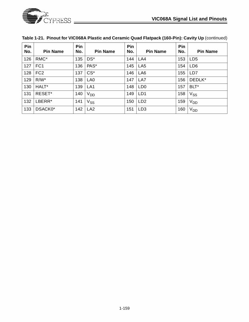
VIC068A Signal List and Pinouts
1-159
126 RMC* 135 DS* 144 LA4 153 LD5
127 FC1 136 PAS* 145 LA5 154 LD6
128 FC2 137 CS* 146 LA6 155 LD7
129 R/W* 138 LA0 147 LA7 156 DEDLK*
130 HALT* 139 LA1 148 LD0 157 BLT*
131 RESET* 140 VDD 149 LD1 158 VSS
132 LBERR* 141 VSS 150 LD2 159 VDD
133 DSACK0* 142 LA2 151 LD3 160 VDD
Table 1-21. Pinout for VIC068A Plastic and Ceramic Quad Flatp ack (160-Pin): Cavity Up (continued)
Pin No. Pin Name
Pin No. Pin Name
Pin No. Pin Name
Pin No. Pin Name

VIC068A Signal List and Pinouts
1-160
Figure 1-48. VIC068A Pin Grid Array (PGA), Bottom View
A B C D E F G H J K L M N P R
1
2
3
4
5
6
9
10
11
12
13
14
15
7
8
VSS
LD6
LD2
LA7
LA3
LA2
LA1
CS*
PAS*
DSACK0*
HALT*
FC2
SIZ1
BLT*
LD5
LD3
LD0
LA5
LA4
LA0
DSACK1*
LBERR*
R/W*
IPL2
RMC*
SIZ0
IRESET*
ABEN*
LIACKO*
IPL1
DEDLK*
LD7
LD4
LA6
VSS
VCC7
DS*
RESET*
FC1
LBR*
SCON*
LADO
VDD
LIRQ2*
VDD
IPL0
LOCATORPIN
CLK64M
LEDI
LEDO
LIRQ5*
LIRQ1*
LAEN
ASIZ1
LIRQ4*
LIRQ3*
LADI
DDIR
DENIN1*
VSS
DENIN*
SWDEN*
ASIZ0
LIRQ6*
LIRQ7*
VDD
DENO*
ISOBE*
SLSEL1*
ICFSEL*
VSS
VSS8
D06
D07
WORD*
MWB*
SLSEL0*
VCC5
D03
D05
FCIACK*
A01
VSS
D00
D01
D04
A02
A03
A06
BG1OUT*
VSS7
D02
A04
A05
IRQ1*
BG2IN*
BG0OUT*
BG3OUT*
VDD
A07
IRQ2*
IRQ5*
SYSFAIL*
IACKIN*
VSS
VSS
VDD
BERR*
BR2*
BBSY*
BG0IN*
BG3IN*
BG2OUT*
VSS
IRQ3*
IRQ6*
VDD
SYSRE-SET*
IACK*
AS*
AM2
LWORD*
WRITE*
DS1*
BR1*
BR3*
BG1IN*
SYSCLK
IRQ4*
IRQ7*
ACFAIL*
IACKOUT*
DTACK*
AM0
AM1
AM3
AM4
AM5
DS0*
BR0*
VSS
BCLR*
VSSLBG*
LD1

VIC068A Signal List and Pinouts
1-161
Figure 1-49. VIC068A Quad Flatp ack (QFP), Top View
1VSS 120 VSS2VSS 119 VSS3IPL0 118 LBG*4IPL1 117 IRESET*5IPL2 116 SCON*6VDD 115 CLK64M7LAEN 114 ABEN*8LIAKO* 113 LADO9LIRQ1* 112 LADI10LIRQ2* 111 LEDI11LIRQ3* 110 VDD12LIRQ4* 109 LEDO13LIRQ5* 108 DDIR14LIRQ6* 107 DENIN1*15LIRQ7* 106 VSS16ASIZ1 105 DENIN*17ASIZ0 104 DENO*18ICFSEL* 103 SWDEN*19SLSEL1* 102 ISOBE*20VSS 101 VDD21SLSEL0* 100 VSS22WORD* 99 D0723FCIACK* 98 D0624MWB* 97 D0525A1 96 D0426VSS 95 VDD27A2 94 D0328A3 93 D0229A4 92 D0130VDD 91 D0031A5 90 BGOUT3*32A6 89 VSS33A7 88 BGOUT2*34VSS 87 BGOUT1*35IRQ1* 86 BGOUT0*36IRQ2* 85 SYSCLK37IRQ3* 84 BGIN3*38IRQ4* 83 BGIN2*39VSS 82 VSS40VSS 81 VSS
41V
DD
160
VD
D42
VD
D15
9V
DD
43IR
Q5*
158
VS
S44
IRQ
6*15
7B
LT*
45IR
Q7*
156
DE
DLK
*46
VD
D15
5LD
747
SY
SFA
IL*
154
LD6
48A
CFA
IL*
153
LD5
49S
YS
RE
SE
T*
152
LD4
50IA
CK
OU
T*
151
LD3
51IA
CK
IN*
150
LD2
52IA
CK
*14
9LD
153
DTA
CK
*14
8LD
054
AS
*14
7LA
755
VS
S14
6LA
656
AM
014
5LA
557
AM
114
4LA
458
AM
214
3LA
359
AM
314
2LA
260
VS
S14
1V
SS
61V
DD
140
VD
D62
AM
413
9LA
163
AM
513
8LA
064
LWO
RD
*13
7C
S*
65W
RIT
E*
136
PAS
*66
BE
RR
*13
5D
S*
67D
S0*
134
DS
AC
K1*
68D
S1*
133
DS
AC
K0*
69B
R0*
132
LBE
RR
*70
VS
S13
1R
ES
ET
*71
BR
1*13
0H
ALT
*72
BR
2*12
9R
/W*
73B
R3*
128
FC
274
BC
LR*
127
FC
175
BB
SY
*12
6R
MC
*76
BG
IN0*
125
SIZ
177
BG
IN1*
124
SIZ
078
VS
S12
3LB
R*
79V
DD
122
VD
D80
VD
D12
1V
DD
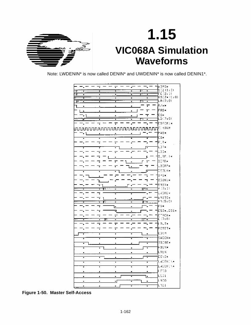
1-162
1.15VIC068A Simulation
WaveformsNote: LWDENIN* is now called DENIN* and UWDENIN* is now called DENIN1*.
Figure 1-50. Master Self-Access

VIC068A Simulation Waveforms
1-163
Figure 1-51. Master Deadlock Operation

VIC068A Simulation Waveforms
1-164
Figure 1-52. Master Write Post

VIC068A Simulation Waveforms
1-165
Figure 1-53. Master Write Post with Slave Read (shows data toggle)

VIC068A Simulation Waveforms
1-166
Figure 1-54. Master RMC1 ($AF [7:5] = 000)

VIC068A Simulation Waveforms
1-167
Figure 1-55. Master RMC2 ($AF [7:5] = 001)

VIC068A Simulation Waveforms
1-168
Figure 1-56. Master RMC3 ($AF [7:5] = 010)

VIC068A Simulation Waveforms
1-169
Figure 1-57. Master RMC4 ($AF [7:5] = 011)

VIC068A Simulation Waveforms
1-170
Figure 1-58. Master RMC5 ($AF [7:5] = 101)

VIC068A Simulation Waveforms
1-171
Figure 1-59. Master RMC6 Non-Byte ($AF[7:5] = 110)

VIC068A Simulation Waveforms
1-172
Figure 1-60. Master RMC7 ($AF [7:5] = 111)

VIC068A Simulation Waveforms
1-173
Figure 1-61. MOVEM Write Operation
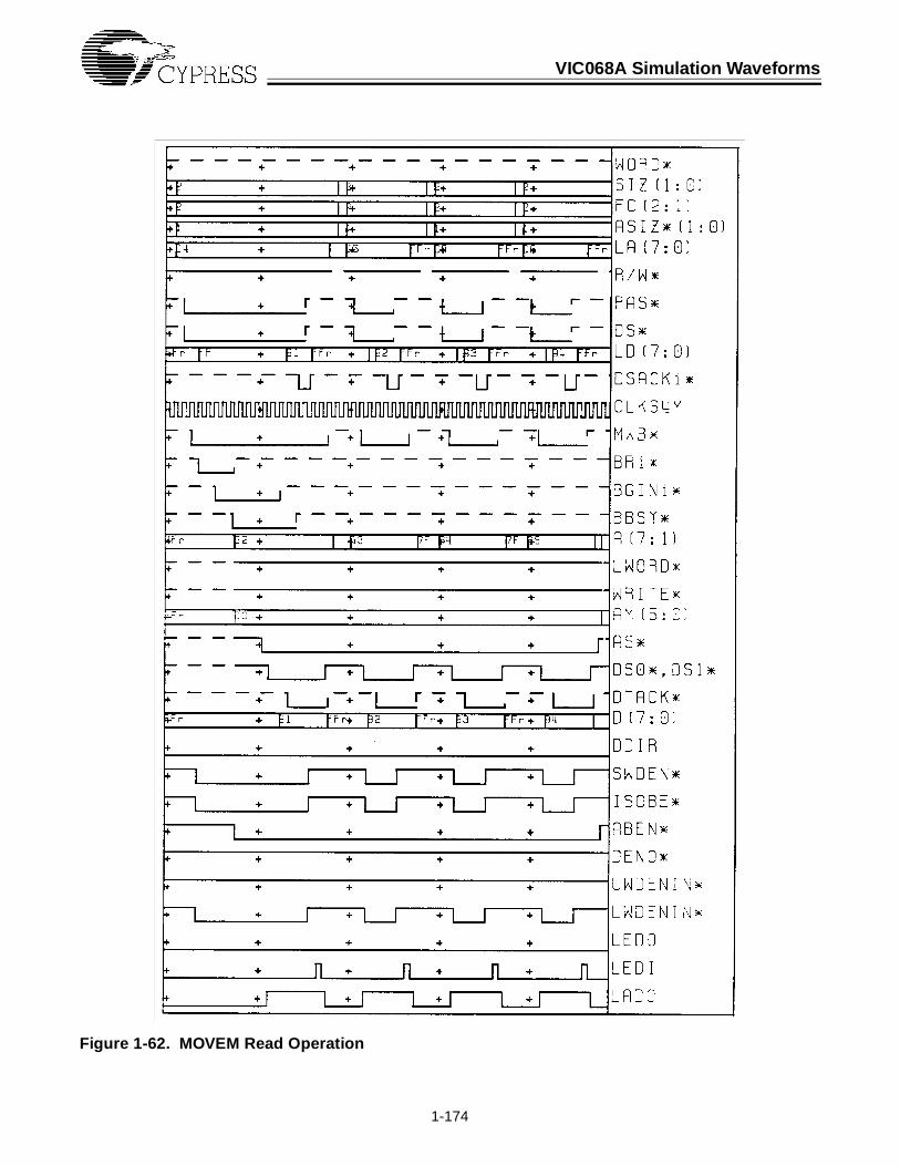
VIC068A Simulation Waveforms
1-174
Figure 1-62. MOVEM Read Operation

VIC068A Simulation Waveforms
1-175
Figure 1-63. Slave Write Post
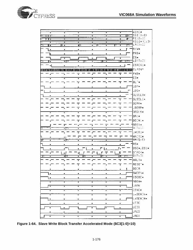
VIC068A Simulation Waveforms
1-176
Figure 1-64. Slave Write Block Transfer Accelerated Mode ($C3[1:0]=10)
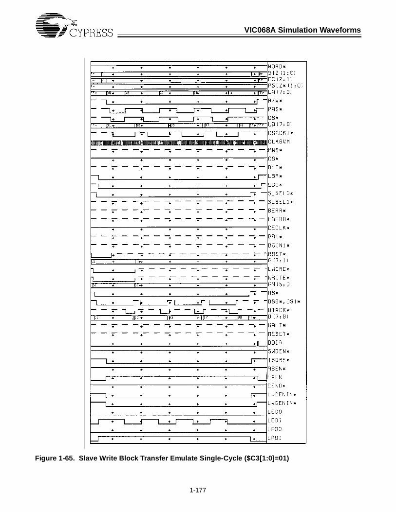
VIC068A Simulation Waveforms
1-177
Figure 1-65. Slave Write Block Transfer Emulate Single-Cycle ($C3[1 :0]=01)

VIC068A Simulation Waveforms
1-178
Figure 1-66. Slave Read Block Transfers Accelerated ($C3[1:0]=10)
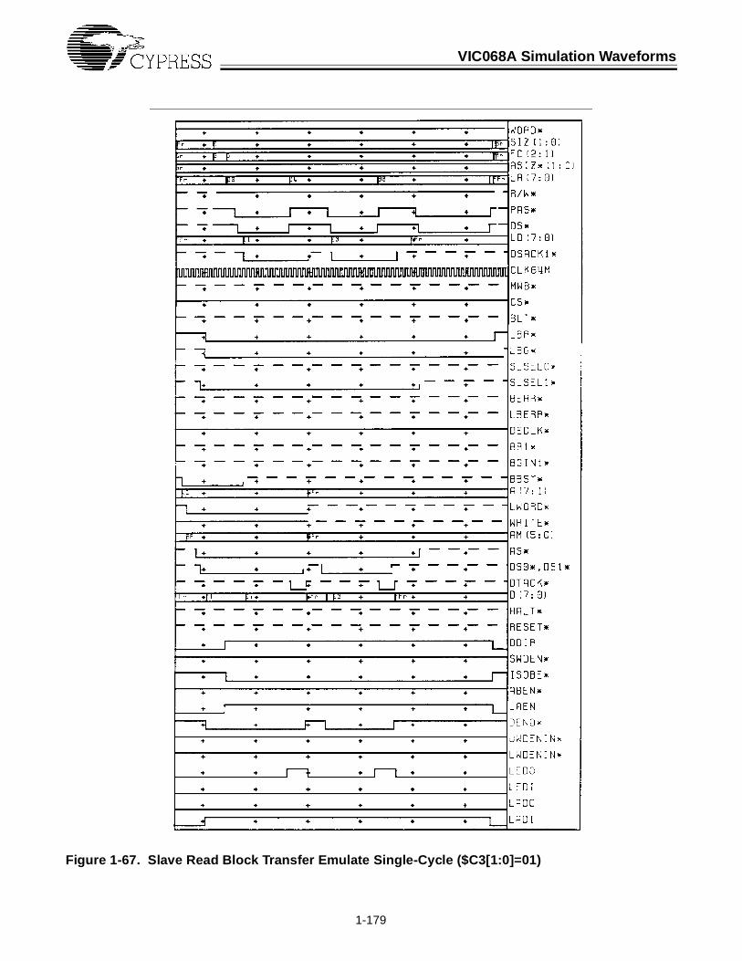
VIC068A Simulation Waveforms
1-179
Figure 1-67. Slave Read Block Transfer Emulate Single-Cycle ($C3[1:0]=01)

VIC068A Simulation Waveforms
1-180
Figure 1-68. Refresh Timing
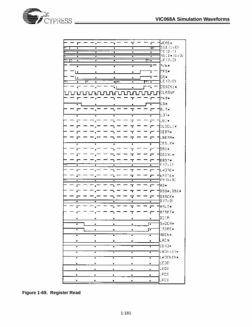
VIC068A Simulation Waveforms
1-181
Figure 1-69. Register Read
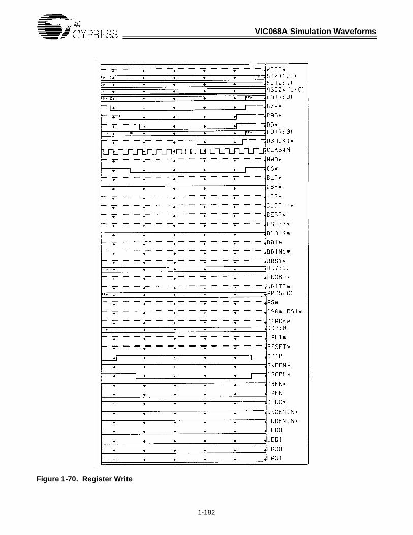
VIC068A Simulation Waveforms
1-182
Figure 1-70. Register Write

VIC068A Simulation Waveforms
1-183
Figure 1-71. Interprocessor Communications Register Access Timing
Figure 1-72. Interprocessor Communication Module Switch Access Timing
Figure 1-73. Interprocessor Communications Global Switch Access Timing
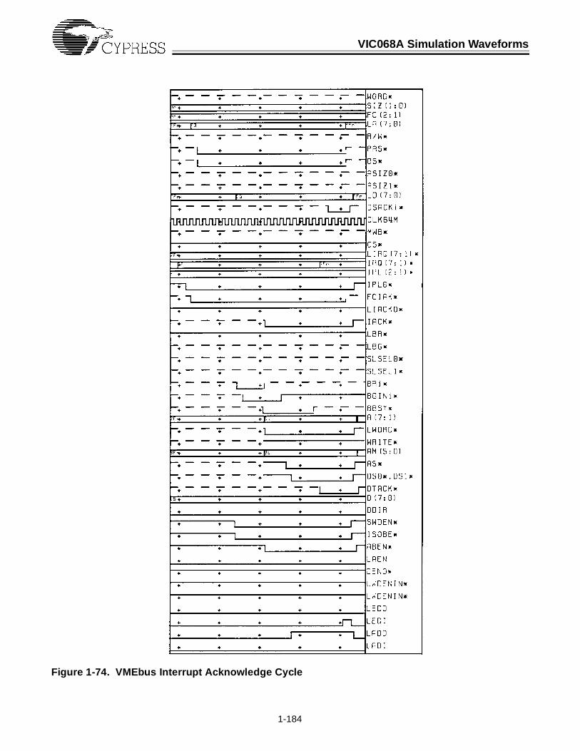
VIC068A Simulation Waveforms
1-184
Figure 1-74. VMEbus Interrupt Acknowledge Cycle

VIC068A Simulation Waveforms
1-185
Figure 1-75. Local Interrupt Acknowledge Cycle

VIC068A Simulation Waveforms
1-186
Figure 1-76. Interrupter Acknowledge Cycle

VIC068A Simulation Waveforms
1-187
Figure 1-77. Block Transfer: VME Write: Burst of 2

VIC068A Simulation Waveforms
1-188
Figure 1-78. VME Boundary Crossing and Local Boundary Crossing

VIC068A Simulation Waveforms
1-189
Figure 1-79. Slave Cycle During Interleave Period

VIC068A Simulation Waveforms
1-190
Figure 1-80. Master Cycle Deadlocked During Interleave

VIC068A Simulation Waveforms
1-191
Figure 1-81. Master Cycle During Interleave with Dual-Path Option

1-192
1.16DC Performance Specifications
.
Table 1-22. VMEbus Signals (AS*, DS1*, DS0*, BCLR*, SYSCLK)
Parameter Description Test Conditions Comm. Industrial Military Units
VIH MinimumHigh-LevelInput Voltage
2.0 2.0 2.0 V
VIL MaximumLow-LevelInput Voltage
0.8 0.8 0.8 V
VOH MinimumHigh-LevelOutput Voltage
VCC = Min.,IOH = –3 mA
2.4 2.4 2.4 V
VOL MaximumLow-LevelOutput Voltage
VCC = Min.,IOL = 48 mA, 56 mA, 64 mA
0.6 0.6 0.6 V
IL MaximumInput LeakageCurrent
VCC = Max.,VIN = 0.6–2.4
±5 ±5 ±5 µA
VIK Input ClampVoltage
VCC = Min. IIN=–18 mA –1.2 –1.2 –1.2 V
VIK Input ClampVoltage
VCC = Min. IIN = 18 mA VCC+1.2 VCC+1.2 VCC+1.2 V
IOZ MaximumOutput LeakageCurrent
VCC = Max.GND < VOUT < VCCAll Outputs Disabled
±10 ±10 ±10 µA

DC Performance Specifications
1-193
.
Table 1-23. VMEbus Signals (Low Drive. All VMEbus Daisy-Chain Signals.)
Parameter Description Test Conditions Comm. Industrial Military Units
VIH MinimumHigh-LevelInput Voltage
2.0 2.0 2.0 V
VIL MaximumLow-LevelInput Voltage
0.8 0.8 0.8 V
VOH MinimumHigh-LevelOutput Voltage
VCC = Min.,IOH = –8 mA
2.4 2.4 2.4 V
VOL MaximumLow-LevelOutput Voltage
VCC = Min.,IOL = 8 mA
0.6 0.6 0.6 V
IL MaximumInput LeakageCurrent
VCC = Max.,VIN = 0.6–2.4
±5 ±5 ±5 µA
VIK Input ClampVoltage
VCC = Min. IIN=–18 mA –1.2 –1.2 –1.2 V
VIK Input ClampVoltage
VCC = Min. IIN = 18 mA VCC+1.2 VCC+1.2 VCC+1.2 V
IOZ MaximumOutput LeakageCurrent
VCC = Max.VOUT = 0.6/2.4VAll Outputs Disabled
±5 ±5 ±10 µA

DC Performance Specifications
1-194
.
Table 1-24. VMEbus Signals (Medium Drive. All non-High, non-Low Drive Signals, All VAC068A VMEbus Signals.)
Parameter Description Test Conditions Comm. Industrial Military Units
VIH MinimumHigh-LevelInput Voltage
2.0 2.0 2.0 V
VIL MaximumLow-LevelInput Voltage
0.8 0.8 0.8 V
VOH MinimumHigh-LevelOutput Voltage
VCC = Min.,IOH = –3 mA
2.4 2.4 2.4 V
VOL MaximumLow-LevelOutput Voltage
VCC = Min.,IOL = 48 mA
0.6 0.6 0.6 V
IL MaximumInput LeakageCurrent
VCC = Max.,VIN = 0.6–2.4
±5 ±5 ±5 µA
VIK Input ClampVoltage
VCC = Min. IIN=–18 mA –1.2 –1.2 –1.2 V
VIK Input ClampVoltage
VCC = Min. IIN = 18 mA VCC+1.2 VCC+1.2 VCC+1.2 V
IOZ MaximumOutput LeakageCurrent
VCC = Max.VOUT = 0.6/2.4VAll Outputs Disabled
±5 ±5 ±10 µA

DC Performance Specifications
1-195
.
.
.
Table 1-25. Non-VMEbus Signals
Parameter Description Test Conditions Comm. Industrial Military Units
VIH MinimumHigh-LevelInput Voltage
2.0 2.0 2.0 V
VIL MaximumLow-LevelInput Voltage
0.8 0.8 0.8 V
VOH MinimumHigh-LevelOutput Voltage
VCC = Min.,IOH = –8 mA
2.4 2.4 2.4 V
VOL MaximumLow-LevelOutput Voltage
VCC = Min.,IOL = 8 mA
0.6 0.6 0.6 V
IL MaximumInput LeakageCurrent
VCC = Max.,VIN = 0.00/VCC
±5 ±5 ±5 µA
VIK Input ClampVoltage
VCC = Min. IIN=–18 mA –1.2 –1.2 –1.2 V
VIK Input ClampVoltage
VCC = Min. IIN = 18 mA VCC+1.2 VCC+1.2 VCC+1.2 V
IOZ MaximumOutput LeakageCurrent
VCC = Max.GND < VOUT < VCCAll Outputs Disabled
±5 ±10 µA
Table 1-26. Capacitance
Parameters Description Test Conditions Max. Units
CIN Input Capacitance TA = 25°C, f = 64 MHz,VCC = 5.0V
5 pF
COUT Output Capacitance 7 pF
Table 1-27. Operating Current
Parameters Description Test Conditions Max. Units
IDD Maximum Operating Current
No external DC load 150 mA

1-196
1.17Package Diagrams
144-Pin Plastic Thin Quad Flat Pack (TQFP) A144

Package Diagrams
1-197
145-Pin Plastic Grid Array (Cavity Up) B144
145-Pin Grid Array (Cavity Up) G145

Package Diagrams
1-198
160-Lead Plastic Quad Flatpack N160

Package Diagrams
1-199
160-Lead Ceramic Quad Flatpack (Cavity Up) U162
Section 2
The VIC64 VMEbus Interface Controller

2-1
2.1Introduction
The VIC64 is a member of the industry-standard VIC family of VMEbus interface products.The VIC64 implements 64-bit wide block transfers, in addition to 32- and 16-bit block transfersand 32-, 16-, and 8-bit single-cycle transfers, all using the same backplane hardware. VIC64is software and hardware compatible with the VIC068A VMEbus Interface Controller.
This document provides the designer with the information needed to evaluate and developVIC64-based boards. You should have already read the section on the VIC068A. This docu-ment provides information on the enhancements found within the VIC64. Another device, theCY7C964 Bus Interface Logic Chip, is described in Section 4 of this book.
Like the Cypress VIC068A, the VIC64 contains all the circuitry necessary to manage VMEbustransfers, either as a slave or a master. It can also be programmed as the VMEbus systemcontroller. The VIC64 contains circuitry intended to minimize the problems associated withthe development of a VMEbus interface such as an interrupt controller, a DMA controller, aDRAM refresh controller, and many other features normally on VMEbus boards. The VIC64is a logical extension to the capabilities of the VIC068A, the industry-standard VMEbus In-terface Controller chip, and it is fully compatible with the VIC068A.
The primary benefit of using the VIC64 is that you can perform 64-bit VMEbus transfers. TheVIC64 also contains some enhancements to the VIC068A, including some performance im-provements and additional features.
A board that has been designed to use the VIC068A is not likely to implement D64 VMEbustransfers, but there are several reasons why a user may choose to replace the VIC068A witha VIC64. For example, to take advantage of the enhancements of the VIC64, or to evaluatethe device and use an existing board to speed the evaluation.

2-2
2.2 Compatibility
All pin assignments and register assignments are the same as those of the VIC068A, thereforethe VIC64 will work flawlessly when used to replace a VIC068A. In fact, several of the VIC068’sfunctions have been enhanced in the VIC64, allowing VIC068A applications to run faster insome cases. Naturally, some attention must be paid to the additional controls for the improvedfunctionality to ensure that the original hardware and software supports the improvements.Therefore, several bits have been added to the VIC068A registers to control the enhance-ments. They map into the unused bits within the VIC068A register space; assuming that theVIC068A developer has not inadvertently set the bits, VIC068A code will run on the VIC64without modification.
To add 64-bit functionality to the VIC family and still retain plug compatibility, the SCON* pinhas been modified in the VIC64. Whereas previously it performed only the input function ofselecting VIC068A to be the system controller, in VIC64 the pin is sensed and latched duringreset to determine whether the system controller function is enabled. After reset the pinbecomes an output to control external circuitry during 64-bit transfers. The new name for thepin is SCON*/D64. If you simply replace the VIC068A with the VIC64, the VIC64 will functionin an identical manner to the VIC068A, whether it is the system controller or not. It is recom-mended that the VIC64 SCON*/D64 pin be connected via a resistive pull-down/up of greaterthan 4.7 kΩ to enable/disable the system controller function.

2-3
2.364-Bit Operations
2.3.1 VMEbus Specification
The primary reason for the development of the VIC64 was to provide users with the capabilityto perform 64-bit-wide data transfers in a manner consistent with the goals of the 64-bitVMEbus specification, more commonly known as the VME64 specification. The protocol for64-bit MBLT (Multiplexed Block Transfer) is specified in an ANSI document VITA1-1994. TheVIC64 implements this protocol.
2.3.2 Address Modifier Codes
VIC64 responds as a slave to the address modifier (AM) codes associated with MBLT transfersas follows:
$3C, $38, $0C, $08; Performs D64 operation as implied by the actual AM code, and thecontents of the Slave configuration Registers $C3 and $CB, and Block Transfer DefinitionRegister $AB.
$00-$07; No response: these codes are associated with 64-bit address operations, and theVIC64 does not support 64-bit address operation.
As a master, VIC64 will use the MBLT protocol to transfer data if the appropriate conditionsoccur:
AM codes $3C, $38, $0C, $08 are selected, and the appropriate bits of the configurationregisters are set (see later for exact details).
In summary, VIC64 performs A32/D64 and A24/D64 operations in addition to the D8/16/32single cycles and A16/24/32..D16/32 block transfers performed by VIC068A.
2.3.3 Boundary Crossing
There are several implications of the 64-bit VMEbus protocol and the requirement for com-patibility that you should consider. The VIC64, being a 144-pin device, can connect to onlythe lower byte of the VMEbus address. For block transfers other than D64 transfers, theVMEbus specification requires that the VMEbus address be rebroadcast at 256-byte bound-ary crossings; this quantity maps neatly into the byte of address that the VIC64 can monitor.MBLT transfers, however, are required to rebroadcast the address only at 2-Kbyte boundaries.VIC64 has no means of determining how the starting address of a master block transfer

64-Bit Operations
2-4
relates to the 2K boundary (it has access to only the lower 8 address bits), and thereforeVIC64 rebroadcasts the address at every 256-byte boundary. This is still compatible with thespecification, but has a small impact on the sustained transfer rate. If you wish to take advan-tage of the increased performance of 2-Kbyte boundaries, then VIC64 can be programmedto rebroadcast the address every 2048 bytes, and the starting address must then be alignedon a 2-Kbyte boundary.
2.3.4 External Circuit Complexity
The VIC64 is a flexible building block that can be used in many different configurations. TheVMEbus specification is written to allow many levels of circuit complexity to conform to thespecification. Such circuitry may include slave address decode circuitry, local DMA transfer,slave read modify cycles, and more. The VIC64 and the VIC068A provide dual-path operation,a mechanism whereby the local bus master can perform single-cycle VMEbus operationsduring the time that the VMEbus is between block transfer bursts (interleave period). Theyalso provide a mechanism allowing master write-posting, and slave read modify cycles tooccur concurrently without harming the posted data. All this circuitry must be duplicatedexternally for the higher-order data byes if you want these features.
You may choose to implement only those features that your system requires, thereby simpli-fying the necessary external circuitry. Alternatively, the user may decide to use the companiondevice, the CY7C964, and gain access to all the features using only three small devices. TheCY7C964 is described in Section 4, The CY7C964 Bus Interface Logic Circuit.

2-5
2.4VIC64:
Additional InformationThe following sections are related to Section 1, The VIC068A VMEbus Interface Controller.The chapter numbers are those chapters of Section 1 that require clarification or modificationfor the VIC64. All other information in Section 1 is applicable to the VIC64.
2.4.1 VIC64 Signal Description (Chapter 1.2)
All pins are identical to those of the VIC068A with the following exception:
SCON*/D64
Input: YesOutput: YesDrive: 16 mA
This is the dual-function signal by which the VIC64 determines whether system controllerfunctions are required, and by which the VIC64 controls external logic during 64-bit VMEbustransfers. During the time that RESET* is asserted, this pin is the SCON* input whose stateis latched internally when RESET* goes inactive. A Low state causes VIC64 to become theVMEbus system controller. During the time that RESET* is inactive, this pin becomes theD64 output whose state is normally Low, becoming High only during the Data Phase of D64transactions.
2.4.2 System Controller Operations (Chapter 1.4)
The VIC64 functions identically to VIC068A as a system controller, except that the SCON*pin of the VIC068A has been renamed to be SCON*/D64 on the VIC64. During the periodthat RESET* is asserted (Low), VIC64 assumes that the pin is an input whose state is latchedon the rising edge of RESET*. The latched state is then used to determine whether the VIC64is the system controller: if the state is Low, then the VIC64 is the system controller.
SCON*/D64 becomes an output after the rising edge of RESET*; the state of the output isused to enable 64-bit data transfers (Chapter 1.10, Block Transfer Functions contains infor-mation on this operation).
2.4.3 VMEbus Master Operations (Chapter 1.5)
The VIC64 does not perform single-cycle 64-bit transfers.

VIC64: Additional Information
2-6
The VIC64 uses the same pins and register bits as the VIC068A to configure and select 64-bit block transfers. The release modes are identical, and the address broadcast phase isidentical to the VIC068A, except that the AM code reflects the D64 transaction (see Table 2-1).
Table 2-1. Master Transfer AM Code Control Map for D64 Operations
As the VIC64 has an identical local bus interface to that of the VIC068A, some mention mustbe made of the protocol used to transfer the 64-bit VMEbus data to the 32-bit local bus. First,it should be noted that Byte(0) is transferred on VMEbus address [A31:A24], and Byte(7) istransferred on VMEbus data [D7:D0]. Two local transactions are required for each VMEbustransaction. For maximization of performance, a pipelined architecture is used. The VIC64provides the appropriate timing for latch controls to implement the pipe externally for thosebytes that the VIC64 itself does not connect to.
2.4.3.1 D64 Master Write Cycles
In the case of master write cycles, the first local cycle fetches the first [Byte(0)–Byte(3)]longword and the VIC64 places it into a two-stage pipe: the next local cycle fetches the nextlongword and presents it to the VMEbus data bus, while the piped data is presented to theVMEbus address bus. Then the next local cycle can commence without waiting for the com-pletion of the VMEbus cycle, as the first stage of the pipe is now free. See the timing diagramsfor full details of this operation.
2.4.3.2 D64 Master Read Cycles
In the case of master read cycles, 64 bits of VMEbus data are latched under the control ofVIC64. The [Byte(4)–Byte(7)] longword is placed into a two-stage pipe, while the [Byte(0)–Byte(3)] longword is presented to the local bus. After the local bus write cycle, the piped datais then presented to the local bus, and the next VMEbus cycle can commence as the firststage of the pipe is now free. See the timing diagrams for full details of this operation.
2.4.4 VMEbus Slave Operations (Chapter 1.6)
Upon detecting SLSEL0* or SLSEL1* asserted, the VIC64 behaves in an identical mannerto the VIC068A except that if the AM code for the slave transaction is $08, $0C, $38, or $3C,the VIC64 configures itself for a D64 slave block transfer (see Table 2-2).
VIC64 Master Access Inputs VIC64 AM Code Output
ASIZ1/0 Address Size Blk FC2 Operation Type AM[5:0]
01 A32 addressing Yes 0X User block $08
01 A32 addressing Yes 1X Supervisory block $0C
11 A24 addressing Yes 0X User block $38
11 A24 addressing Yes 1X Supervisory block $3C

VIC64: Additional Information
2-7
Table 2-2. Slave Transfer AM Code Control Map for D64 Operations
2.4.4.1 D64 Slave Read Cycles
As in the case of master write cycles, the first local cycle fetches the first [Byte(0)-Byte(3)]longword and the VIC64 places it into a two-stage pipe. The next local cycle fetches the nextlongword and presents it to the VMEbus data bus, while the piped data is presented to theVMEbus address bus. Then the next local cycle can commence without waiting for the com-pletion of the VMEbus cycle, as the first stage of the pipe is now free.
2.4.4.2 D64 Slave Write Cycles
As in the case of master read cycles, 64 bits of VMEbus data are latched under the controlof VIC64. The [Byte(4)–Byte(7)] longword is placed into a two-stage pipe, while the [Byte(0)–Byte(3)] longword is presented to the local bus. After the local bus write cycle, the piped datais then presented to the local bus, and the next VMEbus cycle can commence as the firststage of the pipe is now free.
2.4.5 Interrupts (Chapter 1.9)
The VIC64 can be programmed to perform either D8, D16, or D32 interrupt acknowledgecycles. The method by which this is performed is simply to drive the values on SIZ1/0, in asimilar fashion to a master read or write operation. The SIZ1/0 lines are sensed by the VIC64following the assertion of FCIACK* by the local processor. Note that no provision is made fornon-aligned status/ID vector: The VIC64 enables the appropriate local bus drivers for either8-, 16-, or 32-bit Status/ID.
Table 2-3. VIC64 Interrupt Acknowledge Cycle Selection
VIC64 AM Code Inputs VIC64 Master Access Outputs
Operation Type AM[5:0] Address Size Blk FC2/1
User block $08 A32 addressing Yes 00
Supervisory block $0C A32 addressing Yes 00
User block $38 A24 addressing Yes 00
Supervisory block $3C A24 addressing Yes 00
SIZ1/0 VMEbus Data Width
00 32
01 8
10 16
11 32

VIC64: Additional Information
2-8
2.4.6 VIC64 Block Transfer Functions (Chapter 1.10)
As the VIC64 is a superset of the VIC068A, all the VIC068A block transfer functionality isreproduced in the VIC64. The additional features provided by the VIC64 are D64 transfersand performance enhancements.
2.4.6.1 D64 Transfers, VMEbus Boundary Crossing
The VME64 specification allows D64 block transfers to exceed the 256-byte boundary-cross-ing limitation that the original VMEbus specification contains. The new specification allowsfor 2-Kbyte boundaries. As the VIC64 can only discern 8 bits of address, it has no means ofdetermining which 256-byte boundary is the 2048-byte boundary, and therefore the VIC64rebroadcasts the address every 256 bytes unless BTDR[7] is set: this bit causes the addressto be rebroadcast on 2-Kbyte boundaries, but the VIC64 then assumes that the transfer startson the 2-Kbyte boundary.
2.4.7 Miscellaneous Features (Chapter 1.11)
2.4.7.1 Selection of System Controller Functionality
The VIC068A is configured to be system controller by strapping SCON* Low. In VIC64, theSCON”*/D64 pin performs this function: the state of the pin is latched during any of the possibleReset operations, and this state determines whether VIC64 is system controller. Followingthe Reset operation, the SCON*/D64 pin becomes an output whose state controls the externalcircuitry (such as the CY7C964) used during the data phase of D64 transfers. The detailedtiming of this operation depends upon internal states such as DRAM refresh timing, in additionto the external stimuli such as SYSRESET*, IRESET*, and IPL0. Use of an external pull-up/pull-down resistor to determine the state of the SCON* pin during the Reset operation is allthat is required to ensure correct operation.
2.4.7.2 Enhanced Turbo Mode
In addition to the use of ICR[1], another performance enhancement is possible in the VIC64.Setting BTDR[5] reduces the DSACK*-to-DTACK* time defined in the slave select controlregisters by 0.5 clock period for both master and slave block transfers. The reduced timesare 0, 1.5, 2, 2.5, ..., 8.5 clock periods. See the AC Timing Parameters section for details onwhich times are affected by this bit.
2.4.8 Register Map and Descriptions (Chapter 1.12)
There are some differences between the VIC068A and the VIC64 register assignments andcontents.

VIC64: Additional Information
2-9
2.4.8.1 Interprocessor Communications Register 5
2.4.8.2 Block Transfer Definition Register
2.4.8.3 Release Control Register
For non-MBLT operations, the burst length is simply the field contents. A value of 0 in thisfield is interpreted to mean 64.
2.4.8.4 Block Transfer Length Register 2
Name: ICR5Address: $77Description: This register provides the VIC64 revision number.
Name: BTDRAddress: $ABDescription: Configures master block transfers for boundary crossing, dual-path and
user defined address modifiers. There are four additional bits defined for VIC64:
Bit 4(0/0/0)
Enables D64 Master Operations when BTCR[6] is set
Bit 5(0/0/0)
Enables Accelerated Block Transfer Operations as discussed above.
Bit 6(0/0/0)
Enables D64 Slave Operations
Bit 7(0/0/0)
Enables 2-Kbyte boundary crossing for D64 Master Operations. If this bit is set, VIC64 assumes that the transfer is aligned to a 2-Kbyte boundary.
Name: RCRAddress: $D3Description: This register configures the VMEbus release mode, and the burst length
for block transfers with local DMA.Bits 5–0(0/0/0)
For MBLT operations (D64 transfers), the burst length is 4 times the actual field contents. A value of 0 is interpreted to mean 4 x 64.
Name: BTLR2Address: $E7Description: This register provides the most significant byte of the 24-bit value used
to determine the byte count for block transfers with local DMABits 7–0(0/0/0)
Bits 23:16 of the block transfer length.

VIC64: Additional Information
2-10
2.4.9 AC Performance Specifications (Chapter 1.13)
AC Timing for D64 Operations [1]
Operation Notes
Commercial Industrial Military
Min. Max. Min. Max. Min. Max.
Master D64 Block Transfer with Local DMA (Initiation Cycle) [2]
A1 MWB*[0] & PAS*[0] & DS*(0) to BRi*[L]
T+7 2T+32 T+7 2T+33 4T+5 5T+38
A2 MWB*[0] & PAS*[0] & DS*(0) to LADO[H]
T+9 2T+31 T+8 2T+32 T+8 2T+38
A3 MWB*[0] & PAS*[0] & DS*(0) to BLT*[L]
T+9 2T+26 T+8 2T+27 T+8 2T+30
A4 MWB*[0] & PAS*[0] & DS*(0) to DSACK1*[L]
T+11 2T+46 T+10 2T+48 T+10 2T+54
A5 MWB*[0] & PAS*[0] & DS*(0) to DSACK0*[L]
T+11 2T+46 T+10 2T+48 T+10 2T+54
Master D64 Block Transfer Address Broadcast Cycle [2]
B1 DTACK*[0] to LBR*[L] 24 65 20 69 20 75
B2 DTACK*[0] to DSi*[H] 8 24 7 26 7 30
B3 DTACK*[0] to SCON*/D64[H]
16 59 15 62 15 70
Master D64 Block Transfer with Local DMA (Write)
** First Longword Fetch **
C1 DSACKi*[0] and DS*[L] to DS*[H]
2, 3, 4 MBAT0+8 MBAT0+T+36
MBAT0+7 MBAT0+T+38
MBAT0+7 MBAT0+T+42
C2 DSACKi*[0] and DS*[L] to LEDO[H]
2, 3, 4 MBAT0+7 MBAT0+T+33
MBAT0+6 MBAT0+T+35
MBAT0+6 MBAT0+T+36
C3 DSACKi*[0] and DS*[L] to LA(7:0)
2, 3, 4 MBAT0+.5T+9
MBAT0+2T+30
MBAT0+.5T+8
MBAT0+2T+32
MBAT0+.5T+8
MBAT0+2T+35
C4 DS*(H) to DS*[L] 2, 3, 4, 5
T+8 3T+31 T+7 3T+32 T+7 3T+35
** Second Longword Fetch **
C5 DSACKi*[0] and DS*[L] to DS*[H]
2, 4 MBAT1+14 MBAT1+T+46
MBAT1+13 MBAT1+T+48
MBAT1+13 MBAT1+T+52
C6 DSACKi*[0] and DS*[L] to DENO*[L]
4 MBAT1+11 MBAT1+T+37
MBAT1+10 MBAT1+T+39
MBAT1+10 MBAT1+T+42
C7 DSACKi*[0] and DS*[L] to LA(7:0)
2, 4 MBAT1+.5T+9
MBAT1+2T+31
MBAT1+.5T+8
MBAT1+2T+32
MBAT1+.5T+8
MBAT1+2T+35
C8 DSACKi*[0] and DS*[L] to DSi*[L]
6 MBAT1+3T+12
MBAT1+4T+32
MBAT1+3T+10
MBAT1+4T+33
MBAT1+3T+10
MBAT1+4T+36
C9 DSACKi*[0] and DS*[L] to LEDO[L]
4 MBAT1+16 MBAT1+T+56
MBAT1+15 MBAT1+T+57
MBAT1+15 MBAT1+T+64
C10 DS*(H) to DS*[L] 2, 4, 5 T+8 3T+31 T+7 3T+32 T+7 3T+35
C11 DTACK*[0] to DSi*[H] 7 22 6 23 6 25
C12 DTACK*[0] to DENO*[H] 2 8 24 7 26 7 30

VIC64: Additional Information
2-11
Master Block Transfer with Local DMA (Read)
** First Longword Write **
D1 LBG*[0] to DENIN*[L] 2 2T+11 3T+41 2T+10 3T+43 2T+10 3T+48
D2 DTACK*[0] to LEDI[H] 7 2T+6 3T+23 2T+5 3T+24 2T+5 3T+27
D3 DTACK*[0] to DSi*[H] 2, 6 2T+9 3T+28 2T+8 3T+29 2T+8 3T+32
D4 DTACK*[0] to DS*[L] 6 2T+13 3T+36 2T+12 3T+37 2T+12 3T+41
D5 DSACKi*[0] and DS*[L] to DS*[H]
2, 3, 4 MBAT0+8 MBAT0+T+37
MBAT0+7 MBAT0+T+38
MBAT0+7 MBAT0+T+42
D6 DSACKi*[0] and DS*[L] to LEDI[L]
3, 4 MBAT0+13 MBAT0+T+52
MBAT0+12 MBAT0+T+53
MBAT0+12 MBAT0+T+60
D7 DSACKi*[0] and DS*[L] to DENIN1*[L]
3, 4 MBAT0+8 MBAT0+T+35
MBAT0+7 MBAT0+T+36
MBAT0+7 MBAT0+T+41
D8 DSACKi*[0] and DS*[L] to LA(7:0)
2, 3, 4 MBAT0+.5T+9
MBAT0+2T+29
MBAT0+.5T+8
MBAT0+2T+31
MBAT0+.5T+8
MBAT0+2T+35
D9 DSACKi*[0] and DS*[L] to DSi*[L]
3, 4 MBAT0+22 MBAT0+T+56
MBAT0+20 MBAT0+T+58
MBAT0+20 MBAT0+T+64
D10 DS*[H] to DS*[L] 2, 4, 5 T+8 3T+29 T+7 3T+31 T+7 3T+35
** Second Longword Write **
D12 DSACKi*[0] and DS*[L] to DS*[H]
2, 4 MBAT1+8 MBAT1+T+36
MBAT1+7 MBAT1+T+38
MBAT1+7 MBAT1+T+42
D13 DSACKi*[0] and DS*[L] to DENIN1*[H]
2, 4 MBAT1+16 MBAT1+T+56
MBAT1+15 MBAT1+T+59
MBAT1+15 MBAT1+T+66
D14 DSACKi*[0] and DS*[L] to LA(7:0)
2, 4 MBAT1+.5T+9
MBAT1+2T+29
MBAT1+.5T+8
MBAT1+2T+31
MBAT1+.5T+8
MBAT1+2T+35
D15 DSACKi*[0] and DS*[L] to LD(7:0)
2, 4 MBAT1+.5T+12
MBAT1+2T+39
MBAT1+.5T+10
MBAT1+2T+42
MBAT1+.5T+10
MBAT1+2T+48
Master D64 Block Transfer with Local DMA (Boundary Crossing) [2]
E1 DS*[0] to BLT*[H] 3 28 2 30 2 33
E2 DS*[1] to BLT*[L] 3 19 2 20 2 21
E3 DSi*[0] to LADO first tran-sition
3 19 3 20 2 21
E4 DSi*[0] to LADO second transition
3 19 3 20 2 21
Slave D64 Block Transfer Address Broadcast Cycle [2]
F1 DSi*[1] to LBR*[L] 11 36 10 39 10 42
F2 DSi*[0] to DTACK*[L] 2T+9 3T+28 2T+8 3T+29 2T+8 3T+32
F3 DSi*[1] to DTACK*[H] 9 28 8 35 8 39
F4 DSi*[1] to SCON*/D64[H] 10 33 9 35 9 39
F5 DSi*[0] and AS*[0] and SLSELi*[0] to LADI[H]
1.5T+5 2T+25 1.5T+4 2T+26 1.5T+4 2T+29
Slave D64 Block Transfer (Write)
** First Longword Cycle **
G1 DSi*[0] to DS*[L] 2, 4 3T+11 4T+38 3T+10 4T+40 3T+10 4T+44
G2 DSi*[0] to DTACK*[L] 6 2T+9 3T+23 2T+8 3T+24 2T+8 3T+26
G3 DSi*[0] to LEDI[H] 2, 4 T+11 2T+37 T+10 2T+39 T+10 2T+42
Operation Notes
Commercial Industrial Military
Min. Max. Min. Max. Min. Max.

VIC64: Additional Information
2-12
G4 DSACKi*[0] and DS*[L] to DS*[H]
2, 4, 8 SBAT0+8 SBAT0+T+36 SBAT0+7 SBAT0+T+38 SBAT0+7 SBAT0+T+42
G5 DSACKi*[0] and DS*[L] to LEDI[L]
2, 4, 8 SBAT0+13 SBAT0+T+52 SBAT0+12 SBAT0+T+54 SBAT0+12 SBAT0+T+60
G6 DSACKi*[0] and DS*[L] to DENIN1*[L]
2, 4, 8 SBAT0+8 SBAT0+T+31 SBAT0+7 SBAT0+T+33 SBAT0+7 SBAT0+T+37
G7 DSACKi*[0] and DS*[L] to LA(7:0)
2, 4, 8 SBAT0+.5T+9
SBAT0+2T+29
SBAT0+.5T+8
SBAT0+2T+31
SBAT0+.5T+8
SBAT0+2T+35
G8 DS*[H] to DS*[L] 2, 4, 5 T+8 3T+31 T+7 3T+32 T+7 3T+35
** Second Longword Cycle[2, 4] **
G9 DSACKi*[0] and DS*[L] to DENIN1*[H]
SBAT1+20 SBAT1+T+64 SBAT1+19 SBAT1+T+67 SBAT1+19 SBAT1+T+74
G10 DSACKi*[0] and DS*[L] to DS*[H]
SBAT1+11 SBAT1+T+34 SBAT1+10 SBAT1+T+36 SBAT1+10 SBAT1+T+42
G11 DSACKi*[0] and DS*[L] to LA(7:0)
SBAT1+.5T+9
SBAT1+2T+29
SBAT1+.5T+8
SBAT1+2T+31
SBAT1+.5T+8
SBAT1+2T+35
G12 DSACKi*[0] and DS*[L] to LD(7:0)
SBAT1+.5T+11
SBAT1+2T+40
SBAT1+.5T+10
SBAT1+2T+42
SBAT1+.5T+10
SBAT1+2T+48
Slave D64 Block Transfer (Read)
** First Longword Cycle **
H1 DSACKi*[0] and DS*[L] to LEDO[H]
4, 8 SBAT0+7 SBAT0+T+36 SBAT0+6 SBAT0+T+37 SBAT0+6 SBAT0+T+41
H2 DSACKi*[0] and DS*[L] to DS*[H]
4, 8 SBAT0+8 SBAT0+T+39 SBAT0+7 SBAT0+T+41 SBAT0+7 SBAT0+T+45
H3 DSACKi*[0] and DS*[L] to LA(7:0)
2, 4, 8 SBAT0+.5T+9
SBAT0+T+29 SBAT0+.5T+8
SBAT0+T+31 SBAT0+.5T+8
SBAT0+T+35
H4 DS*[H] to DS*[L] 2, 4, 5 T+8 3T+30 T+7 3T+32 T+7 3T+35
** Second Longword Cycle **
H5 DSACKi*[0] and DS*[L] to LEDO[L]
4 SBAT1+19 SBAT1+T+64 SBAT1+18 SBAT1+T+67 SBAT1+18 SBAT1+T+74
H6 DSACKi*[0] and DS*[L] to DENO*[L]
4 SBAT1+11 SBAT1+T+37 SBAT1+10 SBAT1+T+39 SBAT1+10 SBAT1+T+42
H7 DSACKi*[0] and DS*[L] to DS*[H]
2, 4 SBAT1+24 SBAT1+T+72 SBAT1+23 SBAT1+T+75 SBAT1+23 SBAT1+T+85
H8 DSACKi*[0] and DS*[L] and DSi*[0] to DTACK*[L]
4 SBAT1+13 SBAT1+T+33 SBAT1+12 SBAT1+T+34 SBAT1+12 SBAT1+T+38
H9 DSACKi*[0] and DS*[L] to LA(7:0)
2, 4 SBAT1+.5T+9
SBAT1+2T+29
SBAT1+.5T+8
SBAT1+2T+31
SBAT1+.5T+8
SBAT1+2T+35
H10 DS1/0*[1] to DENO*[H] 2 6 21 5 22 5 25
Slave D64 Block Transfer (Boundary Crossing)
H11 DS*[0] to LADI[L] 2 11 26 10 28 10 32
H12 DS*[1] to LADI[H] 2 6 13 5 14 5 15
Operation Notes
Commercial Industrial Military
Min. Max. Min. Max. Min. Max.

VIC64: Additional Information
2-13
Notes:
1. All minimum times are guaranteed, not tested.
2. These timings are specified for information, but not tested.
3. For second and all subsequent longword fetches, MBAT1 is used in the timing equations.
4. When the Enhanced Turbo Bit is set, all these times are reduced by 0.5T.
5. Min. and Max. Times are programmable: see Register Descriptions.
6. When the Enhanced Turbo Bit is set, these times become MBAT1+.5T+D min., MBAT1+1.5T+D max.
7. When the Enhanced Turbo Bit is set, all these items are reduced to 0.5T min., 1.0T max., plus appropriateasynchronous delay from the table. Minimum times reflect unloaded device pins. Actual in-system delays willbe in accordance with the VMEbus specification.
8. For second and all subsequent longword fetches, SBAT1 is used in the timing equations.

VIC64: Additional Information
2-14
Figure 2-1. Master Address Broadcast Cycle
MWB*
R/W*
LA
LD
BLT*
PAS*
DS*
DSACK1*
DSACK0*
A[31:1]+LWORD*
AM[5:0]
D[31:0]
AS*
DS1*
DS0*
DTACK*
WRITE*
DENIN*
DENIN1*
LEDI
LEDO
DENO*
SCON*/D64
LAEN
LADO
LADI
ABEN*
B3
B2

VIC64: Additional Information
2-15
Figure 2-2. Master D64 Write Operation: Detail
MWB*
R/W*
LA
LD
BLT*
PAS*
DS*
DSACK1*
DSACK0*
A[31:1]+LWORD*
AM[5:0]
D[31:0]
AS*
DS1*
DS0*
DTACK*
WRITE*
DENIN*
DENIN1*
LEDI
LEDO
DENO*
SCON*/D64
LAEN
LADO
LADI
ABEN*
C3 C7
C1 C4 C5 C10
C8
C11
C2
C9
C6 C12

VIC64: Additional Information
2-16
Figure 2-3. Master D64 Write Operation: Block Transfer
MWB*
R/W*
LA
LD
BLT*
PAS*
DS*
DSACK1*
DSACK0*
A[31:1]+LWORD*
AM[5:0]
D[31:0]
AS*
DS1*
DS0*
DTACK*
WRITE*
DENIN*
DENIN1*
LEDI
LEDO
DENO*
SCON*/D64
LAEN
LADO
LADI
ABEN*
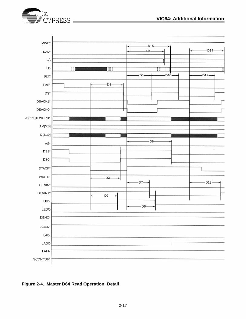
VIC64: Additional Information
2-17
Figure 2-4. Master D64 Read Operation: Detail
D15MWB*
R/W*
LA
LD
BLT*
PAS*
DS*
DSACK1*
DSACK0*
A[31:1]+LWORD*
AM[5:0]
D[31:0]
AS*
DS1*
DS0*
DTACK*
WRITE*
DENIN*
DENIN1*
LEDI
LEDO
DENO*
SCON*/D64
LAEN
LADO
LADI
ABEN*
D4
D2
D3
D6
D7 D13
D9
D5 D10 D12
D8 D14

VIC64: Additional Information
2-18
Figure 2-5. Master D64 Read Operation: Block Transfer
MWB*
R/W*
LA
LD
BLT*
PAS*
DS*
DSACK1*
DSACK0*
A[31:1]+LWORD*
AM[5:0]
D[31:0]
AS*
DS1*
DS0*
DTACK*
WRITE*
DENIN*
DENIN1*
LEDI
LEDO
DENO*
SCON*/D64
LAEN
LADO
LADI
ABEN*
E1 E2
E3 E4

VIC64: Additional Information
2-19
Figure 2-6. Slave D64 Write Operation: Detail
MWB*
R/W*
LA
LD
BLT*
PAS*
DS*
DSACK1*
DSACK0*
A[31:1]+LWORD*
AM[5:0]
D[31:0]
AS*
DS1*
DS0*
DTACK*
WRITE*
DENIN*
DENIN1*
LEDI
LEDO
DENO*
SCON*/D64
LAEN
LADO
LADI
ABEN*
G3
G2
G1
G7
G12
G11
G10
G6
G5
G9
G4 G8
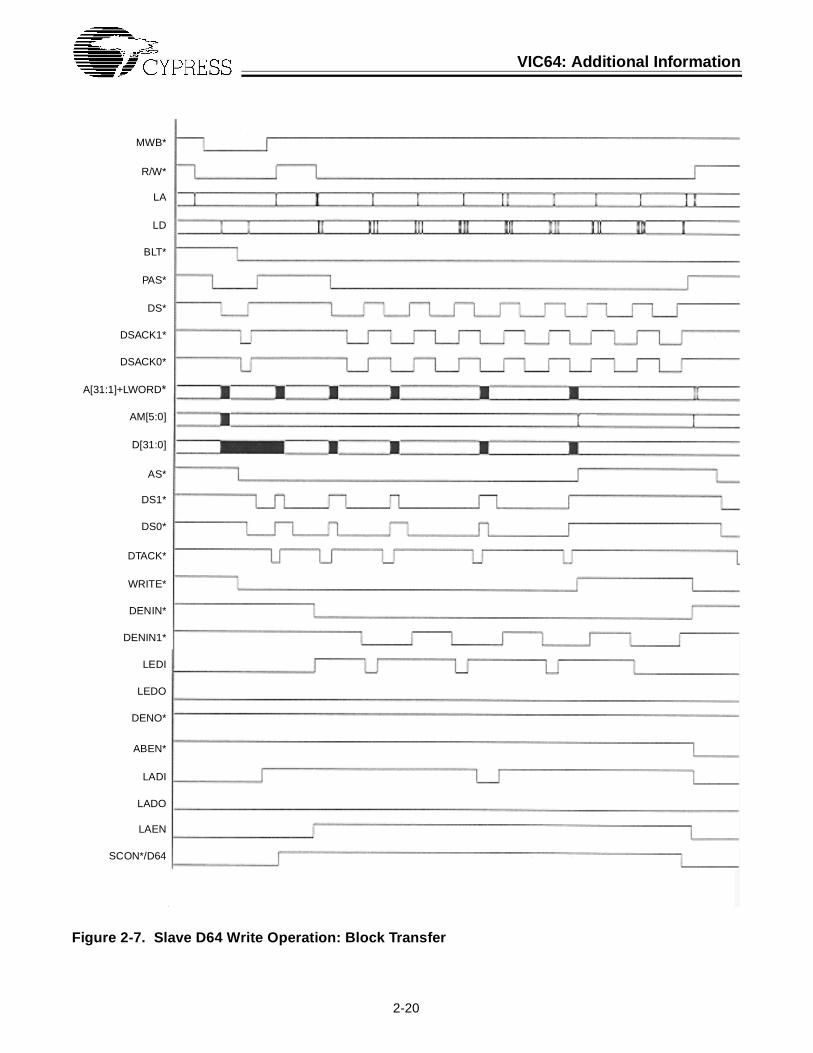
VIC64: Additional Information
2-20
Figure 2-7. Slave D64 Write Operation: Block Transfer
MWB*
R/W*
LA
LD
BLT*
PAS*
DS*
DSACK1*
DSACK0*
A[31:1]+LWORD*
AM[5:0]
D[31:0]
AS*
DS1*
DS0*
DTACK*
WRITE*
DENIN*
DENIN1*
LEDI
LEDO
DENO*
SCON*/D64
LAEN
LADO
LADI
ABEN*

VIC64: Additional Information
2-21
Figure 2-8. Slave D64 Read Operation: Detail
MWB*
R/W*
LA
LD
BLT*
PAS*
DS*
DSACK1*
DSACK0*
A[31:1]+LWORD*
AM[5:0]
D[31:0]
AS*
DS1*
DS0*
DTACK*
WRITE*
DENIN*
DENIN1*
LEDI
LEDO
DENO*
SCON*/D64
LAEN
LADO
LADI
ABEN*
H3
H1
H2 H4
H9
H7
H8
H5
H6
H10

VIC64: Additional Information
2-22
Figure 2-9. Slave D64 Read Operation: Block Transfer
MWB*
R/W*
LA
LD
BLT*
PAS*
DS*
DSACK1*
DSACK0*
A[31:1]+LWORD*
AM[5:0]
D[31:0]
AS*
DS1*
DS0*
DTACK*
WRITE*
DENIN*
DENIN1*
LEDI
LEDO
DENO*
SCON*/D64
LAEN
LADO
LADI
ABEN*
A3
A4
A5
F2
F3
F5
F4
H11 H12

2-23
2.5DC Performance Specifications
Table 2-4. VMEbus Signals (AS*, DS1*, DS0*, BCLR*, SYSCLK)
Parameter Description Test Conditions Comm. Industrial Military Units
VIH MinimumHigh-LevelInput Voltage
2.0 2.0 2.0 V
VIL MaximumLow-LevelInput Voltage
0.8 0.8 0.8 V
VOH MinimumHigh-LevelOutput Voltage
VCC = Min.,IOH = –3 mA
2.4 2.4 2.4 V
VOL MaximumLow-LevelOutput Voltage
VCC = Min.,IOL = 48 mA, 56 mA, 64 mA
0.6 0.6 0.6 V
IL MaximumInput LeakageCurrent
VCC = Max.,VIN = 0.6–2.4
±5 ±5 ±5 µA
VIK Input ClampVoltage
VCC = Min. IIN= –18 mA –1.2 –1.2 –1.2 V
VIK Input ClampVoltage
VCC = Min. IIN = 18 mA VCC+1.2 VCC+1.2 VCC+1.2 V
IOZ MaximumOutput LeakageCurrent
VCC = Max.GND < VOUT < VCCAll Outputs Disabled
±10 ±10 ±10 µA

DC Performance Specifications
2-24
Table 2-5. VMEbus Signals (Low Drive. All VMEbus Daisy-Chain Signals.)
Parameter Description Test Conditions Comm. Industrial Military Units
VIH MinimumHigh-LevelInput Voltage
2.0 2.0 2.0 V
VIL MaximumLow-LevelInput Voltage
0.8 0.8 0.8 V
VOH MinimumHigh-LevelOutput Voltage
VCC = Min.,IOH = –8 mA
2.4 2.4 2.4 V
VOL MaximumLow-LevelOutput Voltage
VCC = Min.,IOL = 8 mA
0.6 0.6 0.6 V
IL MaximumInput LeakageCurrent
VCC = Max.,VIN = 0.6–2.4
±5 ±5 ±5 µA
VIK Input ClampVoltage
VCC = Min. IIN= –18 mA –1.2 –1.2 –1.2 V
VIK Input ClampVoltage
VCC = Min. IIN = 18 mA VCC+1.2 VCC+1.2 VCC+1.2 V
IOZ MaximumOutput LeakageCurrent
VCC = Max.VOUT = 0.6/2.4VAll Outputs Disabled
±5 ±5 ±10 µA

DC Performance Specifications
2-25
Table 2-6. VMEbus Signals (Medium Drive. All non-High, non-Low Drive Signals, All VAC068A VMEbus Signals.)
Parameter Description Test Conditions Comm. Industrial Military Units
VIH MinimumHigh-LevelInput Voltage
2.0 2.0 2.0 V
VIL MaximumLow-LevelInput Voltage
0.8 0.8 0.8 V
VOH MinimumHigh-LevelOutput Voltage
VCC = Min.,IOH = –3 mA
2.4 2.4 2.4 V
VOL MaximumLow-LevelOutput Voltage
VCC = Min.,IOL = 48 mA
0.6 0.6 0.6 V
IL MaximumInput LeakageCurrent
VCC = Max.,VIN = 0.6–2.4
±5 ±5 ±5 µA
VIK Input ClampVoltage
VCC = Min. IIN= –18 mA –1.2 –1.2 –1.2 V
VIK Input ClampVoltage
VCC = Min. IIN = 18 mA VCC+1.2 VCC+1.2 VCC+1.2 V
IOZ MaximumOutput LeakageCurrent
VCC = Max.VOUT = 0.6/2.4VAll Outputs Disabled
±5 ±5 ±10 µA
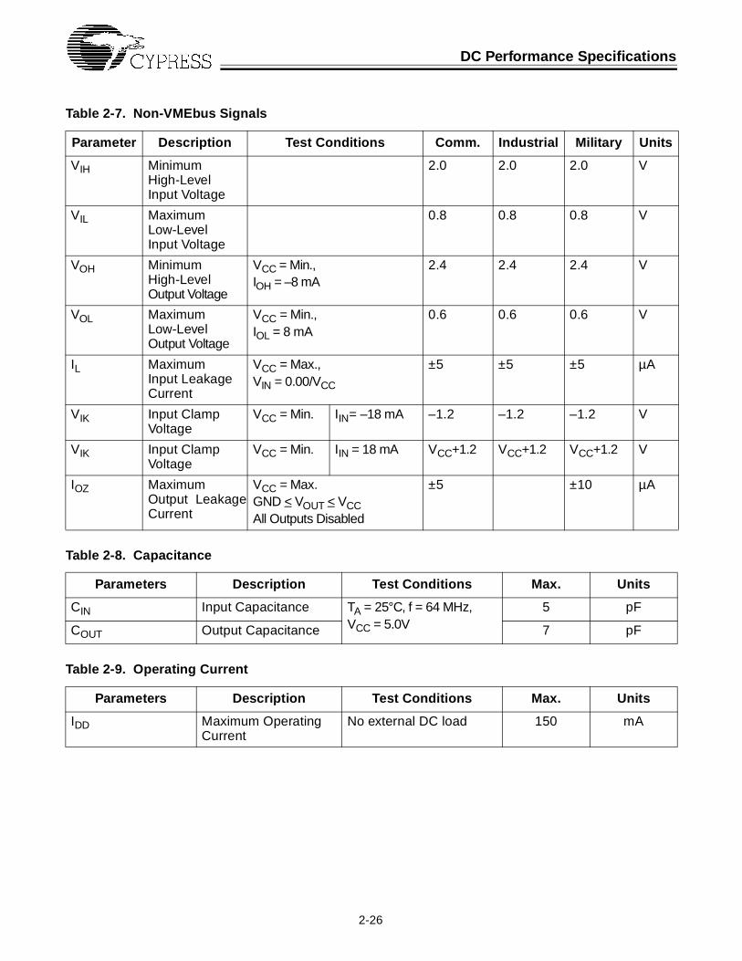
DC Performance Specifications
2-26
Table 2-7. Non-VMEbus Signals
Table 2-8. Capacitance
Table 2-9. Operating Current
Parameter Description Test Conditions Comm. Industrial Military Units
VIH MinimumHigh-LevelInput Voltage
2.0 2.0 2.0 V
VIL MaximumLow-LevelInput Voltage
0.8 0.8 0.8 V
VOH MinimumHigh-LevelOutput Voltage
VCC = Min.,IOH = –8 mA
2.4 2.4 2.4 V
VOL MaximumLow-LevelOutput Voltage
VCC = Min.,IOL = 8 mA
0.6 0.6 0.6 V
IL MaximumInput LeakageCurrent
VCC = Max.,VIN = 0.00/VCC
±5 ±5 ±5 µA
VIK Input ClampVoltage
VCC = Min. IIN= –18 mA –1.2 –1.2 –1.2 V
VIK Input ClampVoltage
VCC = Min. IIN = 18 mA VCC+1.2 VCC+1.2 VCC+1.2 V
IOZ MaximumOutput LeakageCurrent
VCC = Max.GND < VOUT < VCCAll Outputs Disabled
±5 ±10 µA
Parameters Description Test Conditions Max. Units
CIN Input Capacitance TA = 25°C, f = 64 MHz,VCC = 5.0V
5 pF
COUT Output Capacitance 7 pF
Parameters Description Test Conditions Max. Units
IDD Maximum Operating Current
No external DC load 150 mA

2-27
2.6Pin Configurations
144-Pin Thin Quad Flatpack (TQFP)
Top View
GN
D
LBG*
IRQ
5*
IPL0234
IPL1 IRESET*
5
IPL2 SCON*/D64
6
VCC CLK64M
7
LAEN ABEN*
8
LIAKO* LADO
9
LIRQ1* LADI
10
LIRQ2* LEDI
11
LIRQ3* VCC
12
LIRQ4* LEDO
13
LIRQ5*
108
DDIR
14
LIRQ6*
107
DENIN1*
15
LIRQ7*
106
GND
16
ASIZ1
105
DENIN*
17
ASIZ0
104
DENO*
18
ICFSEL*
103
SWDEN*
19
SLSEL1*
102
ISOBE*
20
GND
101
VCC
21
SLSEL0*
100
GND
22
WORD*
99
D07
23
FCIACK*
98
D06
24
MWB*
97
D05
25
A1
96
D04
26
GND
95
VCC
27
A2
94
D03
28
A3
93
D02
29
A4
92
D01
30
VCC
91
D00
31
A5
90
BGOUT3*
32
A6
89
GND
33
A7
88
BGOUT2*
34
GND
87
BGOUT1*
35
IRQ1*
86
BGOUT0*
36
IRQ2*
85
SYSCLKIRQ3*
84
BGIN3*IRQ4*
83
BGIN2*
8281
41 42 43 44
IRQ
6*B
LT*
45
IRQ
7*D
ED
LK*
46
VC
CLD
7
47
SY
SFA
IL*
LD6
48
AC
FAIL
*LD
5
49
SY
SR
ES
ET
*LD
4
50
IAC
KO
UT
*LD
3
51
IAC
KIN
*LD
2
52
IAC
K*
LD1
53
DTA
CK
*LD
0
54
AS
*LA
7
55
GN
DLA
6
56
AM
0LA
5
57
AM
1LA
4
58
AM
2
143
LA3
59
AM
3
142
LA2
60
GN
D
141
GN
D
61
VC
C
140
VC
C
62
AM
4
139
LA1
63
AM
5
138
LA0
64
LWO
RD
*
137
CS
*
65
WR
ITE
*
136
PAS
*
66
BE
RR
*
135
DS
*
67
DS
0*
134
DS
AC
K1*
68
DS
1*
133
DS
AC
K0*
69
BR
0*
132
LBE
RR
*
70
VS
S
131
RE
SE
T*
71
BR
1*
130
HA
LT*
72
BR
2*
129
R/W
*
123
BR
3*
128
FC
2
122
BC
LR*
127
FC
1
121
BB
SY
*
126
RM
C*
120
BG
IN0*
125
SIZ
1
119
BG
IN1*
124
SIZ
0
118
GN
DLB
R*
117
116
37 38 39 40
8079787776757473
115
114
113
112
111
110
109
144
1

Pin Configurations
2-28
160-Pin Quad Flatpack (QFP)
Top View
1GND 120 GDN2GND 119 GND3IPL0 118 LBG*4IPL1 117 IRESET*5IPL2 116 SCON*/D646VCC 115 CLK64M7LAEN 114 ABEN*8LIAKO* 113 LADO9LIRQ1* 112 LADI10LIRQ2* 111 LEDI11LIRQ3* 110 VCC12LIRQ4* 109 LEDO13LIRQ5* 108 DDIR14LIRQ6* 107 DENIN1*15LIRQ7* 106 GND16ASIZ1 105 DENIN*17ASIZ0 104 DENO*18ICFSEL* 103 SWDEN*19SLSEL1* 102 ISOBE*20GND 101 VCC21SLSEL0* 100 GND22WORD* 99 D0723FCIACK* 98 D0624MWB* 97 D0525A1 96 D0426GND 95 VCC27A2 94 D0328A3 93 D0229A4 92 D0130VCC 91 D0031A5 90 BGOUT3*32A6 89 GND33A7 88 BGOUT2*34GND 87 BGOUT1*35IRQ1* 86 BGOUT0*36IRQ2* 85 SYSCLK37IRQ3* 84 BGIN3*38IRQ4* 83 BGIN2*39GND 82 GND40GND 81 GND
41V
CC
160
VC
C42
VC
C15
9V
CC
43IR
Q5*
158
GN
D44
IRQ
6*15
7B
LT*
45IR
Q7*
156
DE
DLK
*46
VC
C15
5LD
747
SY
SFA
IL*
154
LD6
48A
CFA
IL*
153
LD5
49S
YS
RE
SE
T*
152
LD4
50IA
CK
OU
T*
151
LD3
51IA
CK
IN*
150
LD2
52IA
CK
*14
9LD
153
DTA
CK
*14
8LD
054
AS
*14
7LA
755
GN
D14
6LA
656
AM
014
5LA
557
AM
114
4LA
458
AM
214
3LA
359
AM
314
2LA
260
GN
D14
1G
ND
61V
CC
140
VC
C62
AM
413
9LA
163
AM
513
8LA
064
LWO
RD
*13
7C
S*
65W
RIT
E*
136
PAS
*66
BE
RR
*13
5D
S*
67D
S0*
134
DS
AC
K1*
68D
S1*
133
DS
AC
K0*
69B
R0*
132
LBE
RR
*70
VS
S13
1R
ES
ET
*71
BR
1*13
0H
ALT
*72
BR
2*12
9R
/W*
73B
R3*
128
FC
274
BC
LR*
127
FC
175
BB
SY
*12
6R
MC
*76
BG
IN0*
125
SIZ
177
BG
IN1*
124
SIZ
078
GN
D12
3LB
R*
79V
CC
122
VC
C80
VC
C12
1V
CC

Pin Configurations
2-29
A B C D E F G H J K L M N P R
1
2
3
4
5
6
9
10
11
12
13
14
15
7
8
A02IPL2 LIACKO*
LOCATOR
LIRQ2* ASIZ1
ICFSEL*VCC
SLSEL1* GNDVCCFCIACK*
LD6 MWB*
Pin Grid Array (PGA)
LIRQ5* ASIZ0GND WORD* A04 IRQ4*
BLT* IPL1 LIRQ1* LIRQ4* LIRQ6* A01 A03 A05 A07 IRQ3* IRQ7*
IRQ2* IRQ6*IRQ1*A06GNDSLSEL0*GNDLIRQ7*LIRQ3*IPL0LD2 LD5
LD1 LD3
LD0 LD4LA7
LA3 LA5 LA6
LA2 LA4
LA1 LA0
CS* DS*
PAS*
IRQ5* VCC
VCC
VCC
VCC D00
D01
D04
D03
D05
D06
D07 D02
GNDGND
GND
GND
GNDVCC
GND
LD7
GND
GND
BGOUT0*
BGOUT3* BGOUT2*
BGIN2*BGOUT1* BGIN0*
BGIN3* BGIN1* BCLR*
BBSY* BR1*
BR3*
BR2* DS1* DS0*
BR0*
LEDO
LEDILADO
LADIFC2
FC1
SCON*/D64
DDIR DENIN* DENO*
SIZ0
SIZ1
LBG* ABEN*
IRESET*
HALT*
DSACK0*
LBR*RMC*
R/W*
DSACK1*
RESET*LBERR*
VCC
CLK64M
DENIN1* SWDEN* ISOBE* SYSCLK
BERR* WRITE* AM5
AM3AM2
AM1
AM0
AM4
AS*
LWORD*
DEDLK* LAEN ACFAIL*
IACKOUT*
SYSFAIL* SYSRE-SET*
IACKIN* IACK*
DTACK*
Bottom View

2-30
2.7Package Diagrams
144-Pin Plastic Thin Quad Flat Pack (TQFP) A144

Package Diagrams
2-31
145-Pin Plastic Grid Array (Cavity Up) B144
145-Pin Grid Array (Cavity Up) G145

Package Diagrams
2-32
160-Lead Plastic Quad Flatpack N160

Package Diagrams
2-33
160-Lead Ceramic Quad Flatpack (Cavity Up) U162

Section 3
The CY7C960/961 Slave VMEbus
Interface Controllers

3-6
3.1Introduction
3.1.1 Feature List
Optimal Performance: 80 Mbyte per second Block Transfer Rates
Next-Generation Product: VME64 transactions, including A64/D64, A40/MD32
transfers, Auto Slot ID, CR/CSR space, LOCK cycles etc.
Backwards Compatible: All standard VMEbus transactions implemented
VMEbus Interrupter
Simple to Use: No Local CPU required
Programmable from VMEbus or serial PROM
Highly Integrated: DRAM controller, including refresh timers,
Local I/O controller,
Innovative Architecture: Flexible VMEbus address scheme
User-configured VMEbus Personality
Ultra-Small footprint: TQFP Packaging, and other options.
3.1.2 Family Overview
The CY7C960 and the CY7C961 are members of Cypress’s industry-standard range of VME-bus controllers. Although they are each low cost, they are highly flexible, and designed tomeet the needs of high performance VMEbus board developers. The CY7C960 is intendedfor applications whose primary requirement is board space savings—it offers Slave-onlyfeatures. The CY7C961 provides Master support in addition to the Slave features of the ‘960,and hence occupies a little more board space. Each device has been optimized for VMEbusperformance, supporting the full 80-Mbyte/sec transfer rate of the VME64 specification.
The other members of the family are VIC068A (the industry’s most popular 32-bit VMEbusinterface controller), VIC64 (the 64-bit version of the VIC068A), VAC068A (VMEbus addresscontroller), and CY7C964 (a useful companion for either VIC068A, VIC64, CY7C960, orCY7C961).
This Section of the book first describes the CY7C960, then extends that description to theCY7C961. It is necessary to understand the operation of the CY7C960 before reading theCY7C961 sections.

Introduction
3-7
3.1.3 CY7C960 Architectural Overview
The CY7C960 Slave VMEbus Interface Controller provides the board designer with an inte-grated, full-featured VME64 interface. This 64 pin device can be programmed to handle everytransaction defined in the VME64 specification. The CY7C960 contains all the circuitry neededto control large DRAM arrays and local I/O circuitry without the intervention of a local CPU.There are no registers to read or write, no complex command blocks to be constructed inmemory. The CY7C960 simply fetches its own configuration parameters during the power-on reset period. After reset the CY7C960 responds appropriately to VMEbus activity andcontrols local circuitry transparently.
Figure 3-1. Typical System Block Diagram
The CY7C960 controls a bridge between the VMEbus and the local DRAM and I/O. Onceprogrammed, the CY7C960 provides activities such as DRAM refresh and local I/O hand-shaking in a manner which requires no additional local circuitry. The VMEbus control signalsare connected directly to CY7C960. The VMEbus address and data signals are connectedto companion address/data transceivers which are controlled by CY7C960. The CY7C964VMEbus Interface Logic Circuit is an ideal companion device: the CY7C964 provides a sliceof data and address logic that has been optimized for VME64 transactions. In addition toproviding the specified drive strength and timing for VME64 transactions, the CY7C964 con-tains all the circuitry needed to multiplex the address/data bus for multiplexed VMEbus trans-actions. It contains counters and latches needed during block transfer (BLT) operations. Andit also contains address comparators which can be used in the board’s Slave Address De-
VMEbus
Add
ress
Dat
a
Con
trol
CY7C960 ControlCY7C964
(x 4)
Add
ress
Dat
a
Con
trol
Local Bus
Dat
a
I/O
Add
ress
Dat
a
DRAM

Introduction
3-8
coder. For a 6U or 9U application, four CY7C964 devices are controlled by a single CY7C960.For 3U applications, the CY7C960 controls two CY7C964 devices and an address latch.
If the application does not need VME64 transactions, then the user may choose to implementthe companion logic using Cypress’s inexpensive FCT family of interface devices. TheCY7C960 also provides all of the timing and control signals needed for this application also.(See Chapter 3.7.)
The design of the CY7C960 makes it unnecessary to know the details of the VMEbus trans-action timing and protocol. The complex VMEbus activities are translated by the CY7C960to be simple local cycles involving a few familiar control signals. Similarly, it is not necessaryto understand the operation of the companion device, CY7C964: all control sequences forthe part are generated automatically by the CY7C960 in response to VMEbus or local activity.If more information is desired, consult Section 4, The CY7C964 Bus Interface Logic Circuit.
VMEbus Transactions supported by CY7C960 include all transactions defined by the VME64specification. CY7C960 functions as a VMEbus Interrupter, and supports the new Auto SlotID standard and CR/CSR space. CY7C960 also handles LOCK cycles, although full LOCKsupport is not possible within the constraints of the CY7C960 pinout. (For full LOCK supportsee the CY7C961 description.)
On the local side, no CPU is needed to program the CY7C960, nor to manage transactions.All programmable parameters are initialized through the use of either the VMEbus, or a serialPROM. As the CY7C960 incorporates a reliable power-on reset circuit, parameters are self-loaded by the device at power-up or after a system reset. If the VMEbus is used to provideparameters, a VMEbus Master provides the programming information using a protocol, de-scribed in a later section, which is compliant with the Auto Slot ID protocol from the VME64specification.
Figure 3-2 shows the internal blocks that comprise the CY7C960. The architecture includesseveral functions that remove most of the VMEbus problems from the board designer’s shoul-ders. All VMEbus control and response is automatic: the user loads the Region/AM tableduring configuration, and the CY7C960 then handles all appropriate VMEbus transactions.The CY7C964 controller works in lock step with the VMEbus Control Interface, providing thecorrect timing and control for the transaction in process. Local circuitry such as DRAM or I/O is simplified by the Refresh Controller, the DRAM Controller, and the Output Pattern Table.Block transfers are supported by the Local Address Controller together with the CY7C964circuitry. Local timing is determined during configuration, and handshaking is available fromthe Data Byte Enable Controller. Local Interrupts are supported through the VME InterruptInterface. The CY7C960 contains an internal Power-on Reset circuit, and responds also to aVMEbus SYSRESET*.
To keep the size of the package as small as possible, several signal pins carry multiplexedsignals, and other pins have functions that are programmable.
The Pin Description section, and other parts of this document, provide full information on thedefinition and use of these multiplexed signals.
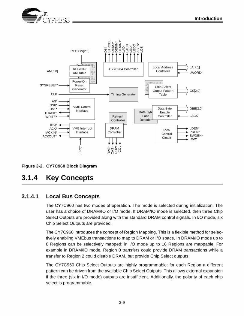
Introduction
3-9
Figure 3-2. CY7C960 Block Diagram
3.1.4 Key Concepts
3.1.4.1 Local Bus Concepts
The CY7C960 has two modes of operation. The mode is selected during initialization. Theuser has a choice of DRAM/IO or I/O mode. If DRAM/IO mode is selected, then three ChipSelect Outputs are provided along with the standard DRAM control signals. In I/O mode, sixChip Select Outputs are provided.
The CY7C960 introduces the concept of Region Mapping. This is a flexible method for selec-tively enabling VMEbus transactions to map to DRAM or I/O space. In DRAM/IO mode up to8 Regions can be selectively mapped: in I/O mode up to 16 Regions are mappable. Forexample in DRAM/IO mode, Region 0 transfers could provide DRAM transactions while atransfer to Region 2 could disable DRAM, but provide Chip Select outputs.
The CY7C960 Chip Select Outputs are highly programmable: for each Region a differentpattern can be driven from the available Chip Select Outputs. This allows external expansionif the three (six in I/O mode) outputs are insufficient. Additionally, the polarity of each chipselect is programmable.
1001001101100101101100110001101010000000100010101011111
1001001101100101101100110001101010000000100010101011111110001110011011001100000000000000
RefreshController
Data ByteLane
Decoder
VME ControlInterface
AS*DS0*DS1*
DTACK*WRITE*
CY7C964 Controller
D64
ST
RO
BE
DE
NO
*D
EN
IN*
DE
NIN
1*LA
DI
LAE
NLE
DI
LED
OA
BE
N*
LDS
Timing Generator
DRAMController
RA
S*
CA
S*
RO
WC
OL
SYSRESET*Power-On
ResetGenerator
VME InterruptInterface
IRQ*IACK*
IACKIN*IACKOUT*
LIR
Q*
REGION/AM TableAM[5:0]
REGION[2:0]
Local AddressController
LA[7:1]
Data ByteEnable
Controller
DBE[3:0]
Chip SelectOutput Pattern
TableCS[2:0]
LACK
LocalControlCircuit
PREN*
R/W*SWDEN*
LDEN*
CLK
LWORD*
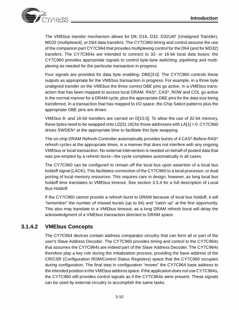
Introduction
3-10
The VMEbus transfer mechanism allows for D8, D16, D32, D32UAT (Unaligned Transfer),MD32 (multiplexed), or D64 data transfers. The CY7C960 timing and control assume the useof the companion part CY7C964 that provides multiplexing control for the D64 (and for MD32)transfers. The CY7C964s are intended to connect to 32- or 16-bit local data buses: theCY7C960 provides appropriate signals to control byte-lane switching, pipelining and multi-plexing as needed for the particular transaction in progress.
Four signals are provided for data byte enabling: DBE[3:0]. The CY7C960 controls theseoutputs as appropriate for the VMEbus transaction in progress. For example, in a three byteunaligned transfer on the VMEbus the three correct DBE pins go active. In a VMEbus trans-action that has been mapped to access local DRAM; RAS*, CAS*, ROW and COL go activein the normal manner for a DRAM cycle, plus the appropriate DBE pins for the data size beingtransferred. In a transaction that has mapped to I/O space; the Chip Select patterns plus theappropriate DBE pins are driven.
VMEbus 8- and 16-bit transfers are carried on D[15:0]. To allow the use of 32-bit memory,these bytes need to be swapped onto LD[31:16] for those addresses with LA[1] = 0. CY7C960drives SWDEN* at the appropriate time to facilitate this byte swapping.
The on-chip DRAM Refresh Controller automatically provides bursts of 4 CAS*-Before-RAS*refresh cycles at the appropriate times, in a manner that does not interfere with any ongoingVMEbus or local transaction. No external intervention is needed on behalf of posted data thatwas pre-empted by a refresh burst—the cycle completes automatically in all cases.
The CY7C960 can be configured to remain off the local bus upon assertion of a local busholdoff signal (LACK). This facilitates connection of the CY7C960 to a local processor, or dualporting of local memory resources. This requires care in design, however, as long local busholdoff time translates to VMEbus timeout. See section 3.5.4 for a full description of LocalBus Holdoff.
If the CY7C960 cannot provide a refresh burst to DRAM because of local bus holdoff, it will“remember” the number of missed bursts (up to 64) and “catch up” at the first opportunity.This also may translate to a VMEbus timeout, as a long DRAM refresh burst will delay theacknowledgment of a VMEbus transaction directed to DRAM space.
3.1.4.2 VMEbus Concepts
The CY7C964 devices contain address comparator circuitry that can form all or part of theuser’s Slave Address Decoder. The CY7C960 provides timing and control to the CY7C964sthat assumes the CY7C964s are indeed part of the Slave Address Decoder. The CY7C964stherefore play a key role during the initialization process, providing the base address of theCR/CSR (Configuration ROM/Control Status Registers) space that the CY7C960 occupiesduring configuration. The final step in configuration “moves” the CY7C964 base address tothe intended position in the VMEbus address space. If the application does not use CY7C964s,the CY7C960 still provides control signals as if the CY7C964s were present. These signalscan be used by external circuitry to accomplish the same tasks.
Introduction
3-11
The CY7C960 recognizes Slave Address Regions which are selected by the use of the 4REGION inputs (3 in DRAM/IO mode). It is the responsibility of the Slave Address Decodercircuitry external to the CY7C960 to drive these pins in response to VMEbus address changes.Thus 16 unique regions (8 in DRAM/IO mode) are recognized by the CY7C960, althoughnormally at least one region would be used as the “Board Not Selected” region.
The CY7C960 is highly flexible in the manner by which it responds to VMEbus transfers. AnAddress Modifier (AM) Code table is configured during initialization which determines whetherspecific AM Codes will be recognized. If a particular code is disabled, then no VMEbus DTACK*is provided and the cycle is ignored. Furthermore, an independent AM Code table is availablefor each of the possible regions in the Slave Address Map. This provides great flexibility tothe user: an I/O region could be configured to respond only to single cycle 8/16 bit transfers,while a DRAM region could be configured to respond only to A64 Block transfers.
3.1.5 Address Mapping
The CY7C960 supports many different schemes for address mapping. The function of theexternal decoder circuitry is to provide signals (REGION[3:0]) to the CY7C960 that definewhether the board is addressed in VMEbus Address Space. One simple use of the CY7C960is shown in Figure 3-3. In this simple case, the CY7C960 has been configured to respondonly to A16 accesses in the VMEbus space 0h–ffffh; to A24 and CR/CSR accesses from10000h–ff ffffh. From 100 0000h–ffff ffffh the CY7C960 responds to A32 accesses, and driveslocal circuitry to route the data to VSB (or Raceway) in the lower part, and to DRAM in theupper part. Above ffff ffffh, the CY7C960 is programmed to respond to A64 or A40 accesses,routing the data to DRAM.
Of course, this fictitious example is impractical due the size of the DRAM segments described.The CY7C960 can support simple contiguous schemes like this one, or arbitrarily complexdecoders at the will of the designer.

Introduction
3-12
Figure 3-3. Possible VMEbus Slave Address Map
0hA16, and I/O
A24 and CR/CSR Space
A32 DRAMSpace
VSB orRaceWay
Space
A64 and A40DRAM Space
ffff ffffh
ffff ffff ffff ffffh
100 0000h
10000h

3-13
3.2 System Block Diagrams
Four examples of system diagrams are shown: a 6U example, a 3U example, a low cost 6Uimplementation, and a CY7C961 3U example.
Figure 3-4 shows an example of a 6U form factor board design. The details of the local circuitryare at the option of the board designer: this diagram illustrates the simplicity of the CY7C960VMEbus interface. Note that in this example, DRAM/IO mode is selected so there are threeregion inputs; the VMEbus is used for configuration as no serial PROM is shown; if AM Codemultiplexing is used, the LA[7:2] pins should be connected to the external address decoderand LADI is used to latch the code in the decoder. As CY7C964s are used, LAEN is requiredto be active High, and hence the internal pull-down resistor is sufficient to define this signalat power-on. No resistors are shown for clarity: see the Pin Description section (Chapter 3.3)for details of which signals are required to be pulled up or down.
The four CY7C964s are controlled by the CY7C960. For more details concerning the con-nection of the CY7C964 to the CY7C960, see the section on CY7C964 Interface (Chapter3.6). The CY7C960 connects directly to the control signals of the VMEbus as shown. TheCY7C964s connect directly to the VMEbus Data and Address bus. If it is desired to support8- and 16-bit VMEbus data transfers to 32-bit memory or peripherals, then the Swap Bufferprovides the data path switching needed to transfer the bytes on the appropriate byte lanes.All timing and control for this comes from the CY7C960. If only 32- and 64-bit transfers arerequired, the swap circuitry is not needed. The decoder block provides the function of SlaveAddress Map decoding, and is user-defined. The CY7C960 ensures that the VMEbus Addressis available on the local address pins at the appropriate times, and the decoder comparesthe value with user-defined inputs. It is the responsibility of the decoder block to provide theREGION[2:0] inputs to the CY7C960. In very simple systems the address comparators withinthe CY7C964s could be used in place of the external decoder block. In Figure 3-4 theCY7C964s are shown providing part of the decoder function (VCOMP* connections).

Introduction to the VIC068A
3-14
Figure 3-4. CY7C960 6U Block Diagram
The DRAM is controlled by the CY7C960, including refresh, and hence the standard connec-tions, RAS*, CAS*, and R/W* are shown. The signals ROW, COL, and DBE, are additionalsignals provided by the CY7C960 to facilitate control of the array. The local handshake, LACK,is shown connected to the DRAM array. In some cases it may be desirable to delay the progressof a DRAM access—LACK can accomplish this. LACK is also used to handshake I/O cyclesif desired. The DBE signals connected to the I/O block provide byte addressing for peripheralsgreater than 8 bits wide.
VME Data Bus D[31:0]
D[3
1:24
]
D[2
3:16
]
D[1
5:8]
D[7
:0]
LD[3
1:16
]
LD[1
5:0]
LA[31:1]
REGION
RAS*, CAS*, ROW, COL
DBE[3:0],R/W*
VCOMP*
VME Address Bus A[31:1], LWORD*
A[3
1:24
]
A[2
3:16
]
A[1
5:8]
A[7
:1],L
WO
RD
*
LA[7:1],LWORD*
DRAMMEMORY
DECODER
I/O
CY7C960
DS
1/0*
VME Interrupt Bus
AM
[5:0
]
SWAPBUFFER
CY7C964 CY7C964
LACK
LIRQ*
DTA
CK
*
IRQ
*AS
*
WR
ITE
*
IAC
KIN
*IA
CK
OU
T*
IAC
K*
SY
SR
ES
ET
*
LA[31:1]
CY7C964 CY7C964
SWDEN*
R/W*
CS[2:0]

Introduction to the VIC068A
3-15
The I/O block is shown providing an interrupt, LIRQ*. This signal causes the CY7C960 toprovide a VMEbus Interrupt. It is the responsibility of the Interrupt Handler and local circuitryto remove the LIRQ* signal at the appropriate time. The CY7C960 merely copies the valueof the LIRQ* through to its IRQ* pin, and handles the IACK cycles appropriately.
The CY7C960 drives the Chip Select outputs in response to a VMEbus cycle. The patternthat is driven can be any binary pattern. In this example, the three available chip selects areprogrammed to provide a different binary pattern for each of the available eight Regions. Theyare connected to the decoder so as to provide a three-to-eight decoder. Thus up to eightperipherals could be selected in this manner.
Figure 3-5 shows a 3U system diagram. In this case there are only two CY7C964s needed,along with one 8-bit address buffer. If the AM Code is connected to the external decoder onpins LA[7:2], then LADI is used to latch the AM Code value in the decoder at the appropriatetime. LAEN is required to be active-High as in the 6U example.
In order to add support for A40/MD32 operations the external decoder would use DENIN*and DENIN1* to enable the local data LD[15:0] into the decoder comparator, making up theupper 16 bits of A[39:0]. The CY7C964s provide the multiplexing for the upper 16 bits of the32-bit data word. The controls for these transactions are provided automatically by theCY7C960. The DBE signals require combinational logic if the local memory or peripheralsare 16 bits wide, as the CY7C960 is designed to control 32-bit local devices. Thus a VMEbusD16 block transfer would activate first DBE[1:0], then DBE[3:2], dependent upon the startingaddress. The DBEs should be logically combined to produce the desired result. Refer tosection 3.6.3, Swap Buffer Control, for more information.
Figure 3-6 shows a low-cost 6U implementation. The VMEbus address and data are bufferedby Cypress FCT parts as shown, controlled by the CY7C960 without additional logic beingrequired. In this case the LAEN is required to be active-Low, accomplished at power on usingthe pull-up resistor externally as shown. As CY7C964s are not used, the functions that thisschematic provides are limited. For example, no multiplexed data transactions, or A64/A40transactions are possible. The external address decoder cannot take advantage of theCY7C964’s on-chip comparators in providing the slave address decode signals REGION[3:0].
Introduction to the VIC068A
3-16
Figure 3-5. CY7C960 3U Block Diagram
Figure 3-7 shows the system diagram for a CY7C961 3U implementation. Note that there areadditional connections to the VME arbitration bus. The block diagram shown supports A40master operations through the use of an external upper address latch. In this implementationthe local DRAM is 32 bits wide, though the VMEbus data connections are only 16 bits wide.A swap buffer comprised of bidirectional transceivers such as the CY74FCT162445 is usedto drive the correct byte lanes of the DRAM, controlled by the CY7C961 automatically. Referto section 3.6.3, Swap Buffer Control, for more information.
VME Data Bus D[31:0]
D[1
5:8]
D[7
:0]
LD[1
5:0
]
LA[23:1]
REGION
RAS*, CAS*, ROW, COL
DBE[3:0],R/W*
VCOMP
VME Address Bus A[31:1], LWORD*
A[1
5:8]
A[7
:1],L
WO
RD
*
LA[7:1],LWORD*
16 bit DRAMMEMORY
DECODER
I/O
CY7C960
DS
1/0*
VME Interrupt Bus
AM
[5:0
]CY7C964
LACK
LIRQ*
DTA
CK
*
IRQ
*AS
*
WR
ITE
*
IAC
KIN
*IA
CK
OU
T*
IAC
K*
SY
SR
ES
ET
*
CS[2:0]
LA[23:1]
’373 CY7C964LADILAEN
A[2
3:16
]

Introduction to the VIC068A
3-17
Figure 3-6. CY7C960 Low-Cost Block Diagram
VCC
LAEN
LADI
R/W*
SWDEN*
LEDI
CY74FCT162245T
CY
74F
CT
1654
3TC
Y74
FC
T1
6543
TC
Y7
4FC
T16
237
3TC
Y74
FC
T16
2373
T
VMEbus P2
VMEbus P1
LD[15:0]
LD[31:16]
CY7C960
LA[31:2]DENIN1*
DENIN*
LEDO
DENO*
A[2
3:1]
, LW
OR
D*
A[3
1:24
]
D[3
1:16
]
D[1
5:0]
>10k
VCC
>10k
Introduction to the VIC068A
3-18
Figure 3-7. CY7C961 3U Block Diagram
These four examples illustrate the flexibility of the CY7C960 and CY7C961 in supporting manydifferent VMEbus and local bus configurations.
VME Data Bus D[31:0]
D[1
5:8]
D[7
:0]
LD[1
5:0]
LA[23:2]
REGION
RAS*, CAS*, ROW, COL
DBE[3:0],R/W*
VME Address Bus A[31:1], LWORD*
A[1
5:8]
A[7
:1],L
WO
RD
*LA[7:1],LWORD*
32 bit DRAMMEMORY
DECODER
I/O
CY7C961D
S1/
0*
VME Interrupt Bus
SWAPBUFFER
CY7C964
LACK
LIRQ*
DTA
CK
*
AS
*
SWDEN*
R/W*
CS[2:0]
AM
[5:0
]
SE
LEC
TLM
*
VME DTB ARBITRATION BUS
IRQ
*WR
ITE
*
IAC
KIN
*IA
CK
OU
T*
IAC
K*B
ER
R*
BR
*B
BS
Y*
BG
IN*
BG
OU
T
VCOMP*
A[2
3:16
]
LED
I
SELECTLM*
LDE
NM
WB
*LA
DO
UPPERADDRESS
LATCH/COUNTER
LA[23:1]
CY7C964
’543LADILAEN321
ABEN*
SY
SR
ES
ET
*

3-19
‘
3.3Pin Description
Figure 3-8. CY7C960 Pin Assignment (TQFP)
3.3.1 VMEbus Signals
AM[5:0] - VMEbus Address Modifier
Input: YesOutput: No
Signals AM[5:0] are the VMEbus Address Modifier inputs. These input signals are used todecode the VMEbus transaction type. The CY7C960 provides support for all predefined anduser-defined VMEbus Address Modifiers.
AS* - VMEbus Address Strobe
Input: YesOutput: NoActive: Low
Address Strobe is the VMEbus signal that informs VMEbus slaves that a valid address is on
the VMEbus. This signal is used by the CY7C960 to qualify the VMEbus Address Modifiers
AM[5:0] and REGION[3:0] inputs to determine if a slave cycle should be performed.
LA7LA6LA5LA4IRQ*LA3GndAM5LA2VccLA1DS1*LWORD*LDSDENIN1*LAEN
PR
EN
*S
WD
EN
*R
AS
*/C
S4
CA
S*/
CS
5A
M2
RO
W/C
S2
CO
L/C
S3
AM
1G
ND
DB
E0
AM
0V
ccD
BE
1D
BE
2D
BE
3R
/W*
LACK*LIRQ*
LDEN*CS0CS1AM3
REGION3/CS2AM4Vcc
GNDREGION2
CLKWRITE*
REGION1REGION0
DENIN*
CY7C960
TQFP
Top View
DE
NO
*IA
CK
OU
T*
IAC
KIN
*IA
CK
*A
S*
LAD
IS
TR
OB
EA
BE
N*
DTA
CK
*G
ND
DS
0*V
ccS
YS
RE
SE
T*
D64
LED
OLE
DI
Pin 1

Pin Description
3-20
DS0*, DS1* - VMEbus Data Strobe
Input: YesOutput: NoActive: Low
DS0* and DS1* are the VMEbus Data Strobe inputs. These signals inform the CY7C960 thateither an address broadcast or data phase of the VMEbus cycle has begun. These signalsin conjunction with the VMEbus LWORD* and LA[1] signals encode the data transfer widthor number of bytes, 1 through 4. This information is necessary to enable the appropriateCY7C964 data bytes.
IRQ* - VMEbus Interrupt Request
Input: NoOutput: YesDrive: 48 mAActive: Low
The IRQ* signal is driven by the CY7C960 to indicate that the local interrupt request signalis active. The IRQ* pin should be connected to one of the 7 VMEbus interrupt request signalsIRQ[7..1]* in order to implement a standard VMEbus interrupt requester. This signal may alsobe used, following a power-on reset, as part of the configuration protocol using the VMEbusto load the device configuration registers. In this case it shall be connected to VMEbus IRQ2*.
IACK* - VMEbus Interrupt
Input: YesOutput: NoActive: Low
The IACK* signal further qualifies the VMEbus address transaction. If this signal is assertedthe CY7C960 decodes the VMEbus address transaction as an Interrupt Acknowledge cycle.During the interrupt acknowledge cycle the CY7C960 will match three bits of the VMEbusaddress (A[3:1]) against the user-programmed internal level. If the levels match, IACKIN* isreceived active, and a VMEbus interrupt is pending from the device, then the VMEbus interruptacknowledge is completed by the enabling of a vector onto the VME data bus. This vector isuser defined, and enabled using the LDEN* signal. CY7C960 assumes that it is an 8-bitinterrupter, and hence responds to all interrupt acknowledge cycles without regard to the sizeof the STATUS/ID requested. If a VMEbus interrupt is not pending or IACKIN* is not assertedto the device this VMEbus address cycle will be disregarded.
IACKIN* - VMEbus Interrupt Acknowledge In
Input: YesOutput: NoActive: Low
The IACKIN* signal informs the CY7C960 that no other up-stream (daisy chain) VMEbusdevice has responded to the VMEbus Interrupt Acknowledge cycle. When IACKIN* is assertedto the CY7C960 during a VMEbus Interrupt Acknowledge, cycle the device determines if a

Pin Description
3-21
VMEbus interrupt is pending of the same level being acknowledged. If so the CY7C960generates a local interrupt acknowledge cycle to respond to the pending interrupt. If a localinterrupt is not pending the device asserts IACKOUT*, passing the chain to the next interrupteron the VMEbus backplane.
IACKOUT* - VMEbus Interrupt Acknowledge Out
Input: NoOutput: YesDrive: 8 mAActive: Low
The CY7C960 asserts the IACKOUT* signal during VMEbus interrupt acknowledge cycles ifthere is no VMEbus interrupt pending on the device, or if the VMEbus interrupt level beingacknowledged does not match that being requested by the CY7C960.
SYSRESET* - VMEbus System Reset Input
Input: YesOutput: NoActive: Low
The SYSRESET* input to the CY7C960 halts all local and VMEbus operations and causesthe device to reinitialize all internal register bits. This reinitialization is either performed byreading the external serial PROM or by an Initialization Master on the VMEbus. When SYS-RESET* goes Low, all outputs from the CY7C960 become three-state until the first risingedge on the CLK input.
WRITE* - VMEbus Write Input
Input: YesOutput: NoActive: Low
The VMEbus WRITE* input encodes the type of VMEbus data cycle in progress. This signalis asserted when a VMEbus WRITE operation is in progress. During such a transaction, ifthe VMEbus address decodes properly, the CY7C960 responds by asserting the local R/Wsignal and performing the appropriate local cycle.
DTACK* - VMEbus Data Acknowledge Output
Input: NoOutput: YesDrive: 64 mAActive: Low
The DTACK* signal is asserted by the CY7C960 when a valid VMEbus transaction is inprogress and the transaction has remained valid for the proper length of time. The assertionof this signal informs the VMEbus Master that the slave has either accepted the data duringwrite operations or has sourced the data during read operations. This signal is a rescindingoutput.

Pin Description
3-22
3.3.2 Local Signals
LWORD* - Long Word
Input: YesOutput: NoActive: Low
This is the local version of the VMEbus signal LWORD* which, when active, indicates eithera D32 or D64 transfer over the VMEbus. The VMEbus LWORD* signal is connected directlyto the A[0] bidirectional pin of the least significant CY7C964. The LA[0] bidirectional pin ofthe least significant CY7C964 is in turn connected directly to the LWORD input of theCY7C960. This signal in conjunction with the DS0*, DS1*, and LA[1] signals encode the datatransfer width or number of bytes, 1 through 4. This information is necessary to enable theappropriate CY7C964 data bytes.
LA[1] / PCLK - Local Address Signal / Init PROM Clock
Input: YesOutput: YesDrive: 8 mA
During CY7C960 initialization this pin sources or receives a serial-PROM-compatible clock.The state of this pin is sampled immediately after the power-on reset period expires. If it issampled High, then the CY7C960 will source a PROM clock signal (PCLK) during localinitialization. If it is sampled Low then the CY7C960 will accept an external clock which willadvance data through its internal serial chain.
If the CY7C960 receives a High data bit on PDATA during the first initialization clock cycle,this signal becomes LA[1] and the device expects to be configured from the VMEbus. If thedevice receives a Low data bit on PDATA during the first initialization clock cycle, the CY7C960will either source or receive a clock from this pin and proceed to load configuration data fromthe local serial data source.
After initialization, this pin carries the local address signal LA[1].
LA[2] / PDATA / AM[0] - Local Address / Init PROM Data / Local AM code
Input: YesOutput: YesDrive: 8 mA
During device initialization the CY7C960 receives the serial data stream on this signal: if thelocal serial method is used, then the serial configuration data comes from the PROM; if theVMEbus method of configuration is used, then the VMEbus A[2] signal is used to carry theserially-encoded configuration data, and the appropriate CY7C964 is enabled by theCY7C960 to provide this data to PDATA. After system initialization this signal becomes localbidirectional address signal LA[2] or LA[2]/AM[0] depending on the programming.
Pin Description
3-23
If the CY7C960 is programmed for LA/AM multiplexing then the VMEbus signals AM[5:0] willbe driven on LA[7:2] by the CY7C960 between VMEbus accesses. A rising edge on LADI isused by local external decoding circuitry to latch the AM codes before this bus changes fromproviding AM information to providing LA information. The CY7C960 will assert LAEN afterLADI rises which disables the CY7C960 LA[7:1] drivers and at the same time enables theCY7C964 LA[7:0] drivers. See section 3.5.3.1.
LA[7:3] / AM[5:1] - Local Address Signals
Input: YesOutput: YesDrive: 8 mA
LA[7:3] make up the remainder of the local bidirectional address bus. The CY7C960 onlysources local addresses during VMEbus block transfer operations. During single cycle andinterrupt acknowledge accesses the lowest order address byte is sourced from the respectiveCY7C964. The CY7C960 begins to source the least significant byte of local address informa-tion starting with the second cycle in a VMEbus block transfer. This is done to increment thelocal address by the proper amount, 1, 2, or 4, depending on the VMEbus word size of thetransfer.
If the CY7C960 is programmed for LA/AM multiplexing, then the VMEbus signals AM[5:0] willbe driven on LA[7:2] by the CY7C960 between VMEbus accesses. A rising edge on LADI isused by local external decoding circuitry to latch the AM codes before this bus changes fromproviding AM information to providing LA information. The CY7C960 will assert LAEN afterLADI rises which disables the CY7C960 LA[7:1] drivers and at the same time enables theCY7C964 LA[7:0] drivers.
PREN* - Serial PROM Enable
Input: NoOutput: YesDrive: 8 mAActive: Low
The PREN* signal enables the serial initialization PROM. The CY7C960 asserts this signalwhen it receives an active SYSRESET* input from the VMEbus or after a power-on resetperiod.
LDEN* - Latch Data Enable
Input: NoOutput: YesDrive: 8 mAActive: Low
The LDEN* signal is used to select one of several potential latched-data sources. During theinitialization sequence LDEN* is driven Low at the time that the Address Mask and Compareregisters of the CY7C964s are to be loaded. After initialization, LDEN* driven low signifiesthat an Interrupt Status/ID or an AUTO ID Status/ID cycle is in progress.

Pin Description
3-24
RAS* / CS[4] - Row Address Strobe / Chip Select 4
Input: NoOutput: YesDrive: 8 mAActive: Programmable
The RAS*/CS[4] output on the CY7C960 is a dual-purpose pin whose function is selectedduring the initialization period. When configured to do so, this output controls the row addressstrobe function for DRAM. In the general-purpose I/O configuration, this output is a user-programmable chip select.
CAS* / CS[5] - Column Address Strobe / Chip Select 5
Input: NoOutput: YesDrive: 8 mAActive: Programmable
The CAS*/CS[5] output on the CY7C960 is a dual-purpose pin whose function is selectedduring the initialization period. When configured to do so, this output controls the columnaddress strobe function for DRAM. In the general-purpose I/O configuration, this output is auser-programmable chip select.
ROW / CS[2] - Row Address Enable / Chip Select 2
Input: NoOutput: YesDrive: 8 mAActive: Programmable
The ROW/CS[2] is a dual-purpose signal whose function is selected during the initializationperiod. When configured to do so, this output acts as a row address enable signal, to be usedin conjunction with RAS. In the general-purpose I/O mode, this output becomes a user-programmable chip select.
When configured for DRAM operation, CY7C960 still provides CS[2] as an output from anotherpin: CS[2]/REGION[3].
COL / CS[3] - Column Address Enable / Chip Select 3
Input: NoOutput: YesDrive: 8 mAActive: Programmable
The COL/CS[3] is a dual-purpose signal whose function is selected during the initializationperiod. When configured to do so, this output acts as a column address enable signal, to beused in conjunction with CAS. In the general-purpose I/O mode, this output becomes a user-programmable chip select.

Pin Description
3-25
DBE[3:0] - Data Byte Enables [3:0]
Input: NoOutput: YesDrive: 8 mAActive: Programmable
These four signals provide the byte enables for local circuitry, either DRAM or I/O. The sizeof the VMEbus data transaction is decoded by CY7C960 from the state of the DS0*/DS1*/LWORD*/A1 VMEbus signals, and the appropriate byte enable signals are driven. The activestate of the signal is user-programmable during configuration. DBE3 represents LD[7:0].DBE0 represents LD[31:24].
CS[1:0] - Chip Select [1:0]
Input: NoOutput: YesDrive: 8 mAActive: Programmable
These two signals are chip select outputs that are available whether the CY7C960 is config-ured for DRAM or for I/O operations. The behavior of these pins is determined during config-uration.
R/W* - Read/Write
Input: NoOutput: YesDrive: 8 mA
R/W* is the local signal that determines if the cycle in progress is a read operation or a writeoperation. The CY7C960 asserts this signal Low during write operations.
LIRQ* - Local Interrupt Request
Input: YesOutput: NoActive: Low
LIRQ* is the local interrupt request input. Asserting this active Low input causes the CY7C960to assert the VMEbus IRQ* output signal.
LACK* - Local Data Acknowledge/Local Bus Hold-off
Input: YesOutput: No
The LACK input is used to acknowledge a local data transfer cycle. Asserting this active Lowsignal causes DTACK* to be driven on the VMEbus. The user may assert this signal contin-uously, which causes the CY7C960 to time data cycle acknowledgments: or the user maywithhold assertion of LACK in order to handshake the acknowledge.

Pin Description
3-26
If the CY7C960 has been programmed for local bus hold-off mode, then LACK is also usedto keep the CY7C960 off the local bus. If LACK is deasserted after LADI falls between VMEbusoperations then the CY7C960 will three-state its local drivers and place itself in stand by untilLACK is asserted again.
REGION[2:0] - Local Slave Decode Inputs
Input: YesOutput: No
The REGION[2:0] inputs are user-programmable address decode inputs. External decodercircuitry, such as the CY7C964’s, drives these signals when VMEbus addresses match user-defined values. CY7C960 uses these signals together with the REGION[3] and AM codes todetermine its reaction to the VMEbus cycle. (See section 3.9.1, Region Mapping.)
CS[2] / REGION[3] - Chip Select [2] / Local Slave Decode Input
Input: YesOutput: YesDrive: 8 mAActive: Programmable
The CS[2]/REGION[3] signal pin has two user-configurable modes of operation. If CY7C960is configured for I/O operation, the pin becomes the REGION[3] input, providing anotherdecode input, a total of 4. If CY7C960 is configured for DRAM, then only three REGION inputsare required, and the pin becomes CS[2]. (See section 3.9.1, Region Mapping.)
CLK - Clock Input
Input: YesOutput: No
The CY7C960 will operate with any input frequency in the range of 30-80 MHz. However, theVMEbus will suffer in performance if this clock is slower than 80MHz. All output events occuron the rising edge of the clock input. All internal states are timed by this signal.
3.3.3 Local Buffer Control Signals
LDS - Local Data Select
Input: NoOutput: YesDrive: 8 mA
During multiplexed data VMEbus transactions this pin is used by the CY7C964s to selectinternal registers. During initialization, this signal determines which of the mask or compareregisters is loaded within the CY7C964s.

Pin Description
3-27
LADI - Latch Address In
Input: NoOutput: YesDrive: 8 mAActive: Programmable
The Latch Address In signal controls the address latches within the CY7C964 that containaddress information to be written to the local bus. The LADI signal is asserted shortly afterthe CY7C960 detects an assertion of the VMEbus AS* signal and can be used externally tolatch local AM codes or LA[31:1] values. In system designs that use the CY7C960 with theCY7C964s this signal can directly connect to the LADI inputs on the CY7C964s.
The state of this pin is sampled immediately after the power-on reset period expires. If it issampled High, then the LADI signal will be active Low. If it is sampled Low, then the LADIsignal will be active High.
LAEN - Local Address Enable
Input: NoOutput: YesDrive: 8 mAActive: Programmable
The Local Address Enable signal enables the local address output buffer within theCY7C964s. The state of this pin is sampled immediately after the power-on reset periodexpires. If it is sampled High, then the LAEN signal will be active Low. If it is sampled Low,then the LAEN signal will be active High.
In system designs that use the CY7C960 with four CY7C964s, this signal is connected to onlythe least significant device and is active High by default via a weak internal pull-down resistor.The LAEN inputs of the other three devices are tied High, or controlled by external logicallowing multi-port local bus accesses. This convention allows the CY7C960 to disable theaddress from the least significant CY7C964 so that it can source the least significant byte oflocal address during block transfer operations.
LEDI - Latch Enable Data In
Input: NoOutput: YesDrive: 8 mA
LEDI is designed to control a transparent latch of the type used within the CY7C964. If thisoutput is Low, data from the VMEbus flows through to the local data bus. Asserting this signalHigh closes the latch, maintaining the data present at the rising edge. System designs thatuse the CY7C960 with CY7C964s can tie this output directly to the associated LEDI input onall of the CY7C964s.

Pin Description
3-28
LEDO - Latch Enable Data Out
Input: NoOutput: YesDrive: 8 mA
LEDO is designed to control a transparent latch similar to the type used within the CY7C964.If this output is Low, data from the local data bus flows through to the VMEbus. Asserting thissignal High closes the latch, maintaining the data present at the rising edge. System designsthat use the CY7C960 with CY7C964s can tie this output directly to the associated LEDOinput on all of the CY7C964s.
DENO* - Data Enable Out
Input: NoOutput: YesDrive: 8 mAActive: Low
The DENO* output controls the VMEbus data bus drivers in the CY7C964s. When data is tobe driven onto the VMEbus, a Low level is driven from this output. A High level on this outputsignifies that the VMEbus drivers are high impedance. This pin should be connected to allthe DENO* pins on the CY7C964s.
DENIN*, DENIN1* - Data Enable In Signals
Input: NoOutput: YesDrive: 8 mAActive: Low
The DENIN* and DENIN1* outputs control the latching of sections of the VMEbus data. Thesetwo control signals in association with the local SWDEN* signal allow all VMEbus transferwidths to be transmitted to the local peripherals. These signals are intended to be connectedto the DENIN* and DENIN1* inputs on all the CY7C964s to enable the local bus drivers. Seesection 3.6.3, Swap Buffer Control.
ABEN* - Address Bus Enable
Input: NoOutput: YesDrive: 8 mAActive: Low
ABEN* is the VMEbus address bus enable out signal. The CY7C960 asserts this signal Lowduring VMEbus D64 block transfer read operations, to enable the second longword of datainformation onto the VMEbus. This output should be connected to the corresponding ABEN*inputs on all four CY7C964s. A pull-up resistor is also needed on this pin for proper operation.

Pin Description
3-29
STROBE - CY7C964 Strobe Control
Input: NoOutput: YesDrive: 8 mA
The STROBE output allows the CY7C960 to control the register loading on the CY7C964s.Loading the CY7C964 Address Mask and Compare registers requires assertion of theSTROBE signal, with the LDS signal providing the signal that determines which of the tworegisters, mask or compare, is loaded. The STROBE output performs this function duringsystem initialization. Designs that use four companion CY7C964s should tie this output to theassociated STROBE input on all four CY7C964 devices.
D64 - CY7C964 D64 Control
Input: NoOutput: YesDrive: 8 mA
The D64 output informs external hardware that a D64 VMEbus block transfer operation is inprogress. When a D64 VMEbus address decode cycle is valid this signal asserts High. De-signs that use four companion CY7C964s should tie this output to the associated D64 inputon all four CY7C964 devices.
SWDEN* - Swap Data Enable
Input: NoOutput: YesDrive: 8 mAActive: Low
The SWDEN* signal controls a local swap buffer. This buffer is used to move data to the propersection of the local data bus during appropriate byte and word width transfers. The CY7C960local bus ordering convention matches that of the MC68020. This signal asserts Low whena byte or word width transfer, which always are moved on D[15:0] of the VMEbus, must endup on D[31:16] of the local data bus. (See section 3.6.3, Swap Buffer Control.)

3-30
3.4 Programming the CY7C960
The VMEbus board that is designed to use the CY7C960 has what might be called a person-ality. This encompasses such things as DRAM (speed and amount), I/O circuitry, SRAM, andother matters under the control of the board designer. To a large extent, this personality hasto be known to the CY7C960. Some portion of this personality is determined when the boardis developed, and is not changed during the board’s lifetime. Other aspects of the personalitycould conceivably change from time to time, such as the address to which the board responds,or the type of VMEbus transaction that it recognizes. All of this information must be providedto the CY7C960 each time the power is cycled or SYSRESET* is asserted. The designermight choose to provide switches that convey part of the personality, or he may rely uponsome other VMEbus board to download the information. The CY7C960 has been designedto support these diverse programming requirements.
First consider the address on the VMEbus to which the board responds. This may be a verysimple application which has only one address range within which to respond; or it may be acomplex address map involving AM Code discrimination, and multiple address ranges. Ineither case, the external address comparator circuitry needs to be programmed with the slaveaddress ranges in which the application will respond. The CY7C960 supports the loading ofthis address comparator circuitry from either local circuitry, or from the VMEbus.
For configuration of the other parameters of the user’s application a serial bit stream is used.The CY7C960 contains approximately 380 programmable bits, each of which must be set tothe right value for the user’s application in order to ensure correct functionality (see Figure3-9). There are two methods that can accomplish this: the VMEbus can be used to passparameters from a VMEbus master to the CY7C960, or a local serial PROM can be used.
Figure 3-9. CY7C960 Initialization Block Diagram
PDATA
REGION/AM
TableDRAM
RAS/CASTiming
RefreshTiming/Enable
ROW/COLPolarity
DBE
DBERefreshEnable
PolarityDBETiming/
REGIONTable
PCLKClock Divider (CLK/80)
DRAM/IOMode
CS
PolarityOutputpattern/
REGIONTable
DecodeDelayTime
Serial Shift Register
Programming the CY7C960
3-31
Thus in summary, the slave address map can be obtained either from local circuitry or theVMEbus, and the configuration data can likewise be obtained either from the VMEbus or fromlocal circuitry.
The CY7C960 is designed for use with the CY7C964 device. The CY7C964’s address andmask registers can be used during the configuration process and the CY7C960 providestiming and control signals during initialization that are intended to load these address andmask registers. If the target application does not use the CY7C964’s registers as part of theslave address decoder, these signals can be used by user-defined circuitry to configure theaddress decoder. Refer to Section 4, The CY7C964 Bus Interface Logic Circuit, for moreinformation regarding the signals used to configure the address and mask registers.
The LAEN signal is programmed during the power-on reset period. This signal is used by theCY7C960 to control the external three-state buffer connected to LA[7:0], enabling theCY7C960 itself to drive LA[7:0] at certain times. If using the CY7C964, LAEN is required tobe active High; other devices may require LAEN to be active Low. During the power-on resetperiod the LAEN pin is sampled to determine whether it is pulled up externally, and if so theLAEN output becomes an active Low signal.
3.4.1 Configuration Bit Stream
The 380 bits that make up the configuration data are provided to the CY7C960 by either aseries of VMEbus transactions, or by a local serial device such as a serial PROM. The variousfields within the bit stream are used to determine the behavior of the CY7C960, and hencethe application, after configuration is complete. For the duration of the configuration processtwo pins, LA[2:1], assume the roles of serial clock and serial data signals. Another pin, PREN*,is used to enable the external serial device during configuration.
The CY7C960 expects the serial data to arrive on pin LA[2] so if the VMEbus configurationmethod is used, it is the responsibility of the remote VMEbus master to encode the desiredconfiguration stream into 380 VMEbus cycles whose VME address A[2] is controlled by thedesired configuration data bit. Likewise, if using a local serial device, the data output from thedevice shall be connected to LA[2].
To assist in the generation of the correct configuration data file, there is a configuration programavailable, called WinSvic, that runs on a PC using Windows. This program has extensive helpmenus which can be used to better understand the configuration bit stream. See section 3.4.6for more details on this development tool.
For applications using a local serial device the serial clock may be generated by the CY7C960,or it may be provided to the CY7C960 by external circuitry.
The CY7C960 determines which method of configuration is desired, and whether to drive aserial clock or not, as part of the power-on process. This is described in the next section.
Programming the CY7C960
3-32
3.4.2 Operation at Power-On or Reset
The CY7C960 contains a power-on reset circuit. When power is applied to the device thiscircuit causes the internal state to be reset. All outputs become three-state until the first risingedge of the clock input is recognized after the internal power-on reset circuit terminates. (Thetime period of the on-chip power-on-reset circuit depends upon the characteristics of thepower supply, but is guaranteed by design to be less than the time period of the rising powerramp.) Also, if a Low level is applied to the SYSRESET* input the CY7C960 immediatelythree-states its output drivers, resets its internal state and waits for the first clock edge beforetaking any action. SYSRESET* does not have to be High for the CY7C960 to commence theconfiguration operation, but must be High for normal operation to proceed after configuration.
PREN* is asserted Low four clocks after the assertion of SYSRESET*, or after a power-onreset. If an external serial device is connected, the first bit must be programmed to be zero.If the VMEbus is to be used, an external pull-up must provide a High level. The PDATA signal(LA[2]) is sensed 40 CLK periods after the assertion of PREN*. If PDATA is sensed to be High,PREN* is driven High one CLK period later.
Also, the CY7C960 senses the level of two pins: LAEN and PCLK (LA[1]). LAEN is sensedto determine whether the signal is desired to be high or low true. PCLK is sensed to determinewhether the pin is to be an input or an output. The point at which these signals are sensed is40 CLK periods after the assertion of PREN*. LAEN has an internal pull-down of approximately470 kohms. PCLK has no internal resistor. Whichever level is sensed on LAEN is driven fromthe pin one clock period after it has been sensed. If PCLK is determined to be pulled High,then it is driven Low by the CY7C960 one CLK period after it was sensed: subsequently theCY7C960 will provide a clock output (of frequency CLK÷80). If PCLK is pulled Low, thenexternal circuitry must provide the serial clock signal and must not drive the PCLK input Highuntil at least 40 CLK periods following the falling edge of PREN*.
If the CY7C960 is providing the PCLK signal, the period of each half-cycle is 40 CLK periods,leading to a PCLK frequency of 1 MHz (CLK÷80). PDATA is required to be stable at eachfalling edge on PCLK, when the PDATA is clocked into the serial configuration register insidethe CY7C960. Similarly, if the PCLK signal is provided externally, the PDATA input must bestable at the falling edge of PCLK. The frequency applied to the PCLK pin from an externalsource does not have to be synchronous to the CLK input as the PCLK input is synchronizedinternally. The minimum half cycle time for the PCLK input is 50 ns: there is no maximum timeas the design is static.
If SYSRESET* is driven Low by a device on the VMEbus, then the CY7C960 reacts in amanner similar to the power-on reset: all outputs become three-state until the first rising edgeof the clock (following the falling edge of SYSRESET*), then the PREN* signal is driven Lowand the initialization cycle commences. Note that the configuration cycle commences priorto the SYSRESET* signal going inactive: this allows the CY7C960 to complete the configu-

Programming the CY7C960
3-33
ration cycle within the 200-ms VMEbus specification for SYSRESET* minimum active time ifthe Serial PROM method is used.
If a front panel reset switch is to be used, then external circuitry combines the two sourcesof reset (VMEbus SYSRESET* and switch reset), and connects the result to the SYSRESET*pin. The behavior of the CY7C960 is, of course, identical in the two different methods ofapplying reset. (Note, however, that if a manual reset is performed while VMEbus activity istaking place, the CY7C960 will ignore any VMEbus transactions to any and all Regions untilthe configuration has been loaded. This may cause the system timer to timeout, and thetransaction will cause a BERR*.)
Following the reset and configuration sequence, the CY7C960 performs a DRAM refreshoperation (if enabled to do so in the configuration sequence). This is illustrated in Figure 3-10. This allows a “warm” reset whereby data in DRAM is preserved across reset operationsthat do not involve power-down. The length of the refresh depends upon the DRAM configu-ration selected during initialization: the possible values are from zero bursts to 128 bursts,each burst being four CAS*-before-RAS* cycles whose cycle timing is taken from the config-ured values. During the long refresh operation, the CY7C960 monitors the VMEbus: if atransaction is directed to the CY7C960 which does not require the use of the DRAM circuitry(for example, a transaction addressed to a Region where DRAM is not enabled), the trans-action is completed normally. If the DRAM access is required, the cycle cannot complete untilthe refresh burst is ended. The detail of the behavior depends upon the transaction: a readoperation of any sort cannot commence until refresh is complete; for write operations, thefirst write cycle is DTACK’ed because the CY7C960 always posts write data, but subsequentwrite cycles will not be acknowledged until the DRAM refresh burst has completed and theposted data has been written to DRAM. In all cases, the CY7C960 completes the transactioncorrectly.
Following the power-on or reset configuration sequence, and the refresh burst (if enabled),the CY7C960 will respond to any VMEbus transfers that are enabled by the configuration.
Figure 3-10. Refresh Burst after Initialization
Reset/Initialization finishesRESET REFRESH BURST (scaled to REFRESH BURST PERIOD)
REFRESH BURST PERIOD
if programmed, DBE follows CAS during refresh bursts.
RAS
CAS
DBE
ROW
COL

Programming the CY7C960
3-34
3.4.3 VMEbus Method
After 40 clock periods, the CY7C960 senses the value of PDATA and PCLK. The VMEbusinitialization method is automatically invoked by the CY7C960 if its PDATA pin is at logic 1 atpower on or during a system reset. (This may be easily accomplished by using a pull-upresistor for the local address bus.) If PDATA is indeed High at this time, then after SYSRESET*is deasserted on the VME backplane, CY7C960 asserts its interrupt request line. This interruptshould be connected to IRQ2* of the VMEbus backplane as the initialization interrupter insideCY7C960 is hard-coded to respond to that level. (After configuration is complete, the user-programmed interrupt level is used, but this must match the actual hardware level connectedon the backplane. Therefore if the user wishes to use a level other than 2, external circuitryis necessary to switch the IRQ output pin to the different VMEbus IRQ signal after initialization.)See section 3.5.6.
The VMEbus Interrupt Handler must provide a level 2 interrupt acknowledge cycle: the inter-rupt acknowledge daisy-chain will ensure that the CY7C960 closest to the handler will respondto the IACK cycle. When the IACK cycle is detected, CY7C960 asserts its LDEN pin, whichprovides a signal for enabling initialization interrupt status ID (user defined) onto the localdata bus. This status comes from user-defined external circuitry such as jumpers or latches.The CY7C964s are controlled by the CY7C960, and hence pass the vector to the VMEbus.CY7C960 will acknowledge the next VMEbus master write qualified by the A16 (supervisoryor nonprivileged) or CR/CSR AM code and write the VMEbus data to the address registersof the CY7C964s. Thus, the CY7C964s are now primed to react to that VMEbus address,unmasked, as the action of writing the compare register clears the mask register in theCY7C964. The interrupt acknowledge cycle and the following single master write cycle mustbe indivisible for guaranteeing system integrity (the board has yet to be positioned in theVMEbus slave address map, and therefore will respond to ANY A16 or CR/CSR write cycle).If this indivisibility is not possible, then the local method of configuration must be used.
From this point, CY7C960 expects a series of A16 (or CR/CSR) master write transactions tobe written to the address just programmed. As the board address has now been set in A16or CR/CSR space, there is no requirement for indivisibility. (There is a requirement that theAM code for each write transaction be the same as that used in the first transaction: start withA16, stay with A16; or start with CR/CSR, stay with CR/CSR.) Each transaction carries asingle configuration bit (just like the serial PROM method). The bit must be encoded on theVMEbus A[2] signal. CY7C960 counts the transactions. After the last transaction of the serialstream is acknowledged, two more transactions are required, with the same address and AMcode. The data from these transactions are loaded into the compare and mask registers ofthe CY7C964s to complete the initialization transaction sequence: the signals that control theloading of the CY7C964 registers are LDS and STROBE (driven by the CY7C960), and MWB*and BLT*, (pulled High).
The REGION[3:0] inputs to the CY7C960 should be driven by the user’s external slave addressmap decoder. For the very first VMEbus write cycle following the IACK cycle, the REGION

Programming the CY7C960
3-35
inputs are ignored. Since the write cycle is not qualified with address (i.e., REGION), it mustimmediately follow the IACK cycle. For subsequent configuration cycles the REGION inputsmust be driven with “xx00” if the CR/CSR AM Code is used; and with “xxx0” (x = don’t-care)if one of the two A16 AM Codes is used. Note that this system allows the user to connect theVCOMP (compare) outputs from the appropriate CY7C964 directly to the related REGIONinput as a simple configuration address map decoder. If the user requires a more complexaddress map, the configuration requirement is easily accomplished.
It should be understood that certain device behavior is not available during the configurationsequence. Obviously, no VMEbus slave operations can take place other than the configurationsequence itself. The CY7C960 does not provide AM Codes from the LA[7:2] pins until afterthe configuration sequence has completed as the bit that enables this operation is embeddedin the configuration sequence. Similarly, the first IACK cycle is self timed because the bit whichenables IACK cycles to be locally handshaked is embedded in the configuration data.
Figure 3-11 shows the timing of the start of the VMEbus initialization sequence, and Figure3-12 shows the end.
In summary, the sequence starts by setting the address of the CR/CSR space, then the CR/CSR is used to load the CY7C960, and finally the board’s Slave Address is loaded. CY7C960exits initialization mode and, after the refresh burst if so enabled, is ready for service. (Notethat this initialization sequence is compliant with the Auto Slot ID utility of the VME64 speci-fication.)

Programming the CY7C960
3-36
Figure 3-11. VMEbus Initialization Start
IRQ LEVEL
IRQ LEVEL
STATID
A16 or CR/CSR
CONTROL ADDRESS
if CR/CSR then ”xx00” if A16 then ”xxx0”
CTRL.
PDATA=1 PDATA=0 PDATA=1
DON’T CARE CTRL. + PDATA CTRL. + PDATA CTRL. + PDATA
STATID
DON’T CARE
SYSRESET*
AM
AS*
IRQ*
IACK*
IACKIN*
IACKOUT*
WRITE*
A
D
DS0*
DS1*
DTACK*
LD
STROBE
REGION
LA
LADI
LAEN
LEDI
LDEN
DENIN
DENO
PREN
LDS

Programming the CY7C960
3-37
Figure 3-12. VMEbus Initialization End
A16 or CR/CSR
COMP. + PDATA COMP. COMP.
PDATA=0
NEW BASE ADDRESS (NBA) ADDRESS MASK
N. B. A. NBA ADDR. MASK
SYSRESET*
AM
AS*
IRQ*
IACK*
IACKIN*
IACKOUT*
WRITE*
A
D
DS0*
DS1*
DTACK*
LD
STROBE
REGION
LA
LADI
LAEN
LEDI
LDEN
DENIN
DENO
PREN
LDS

Programming the CY7C960
3-38
3.4.4 Serial PROM Method
Following the assertion of SYSRESET*, or a power-on reset, CY7C960 drives PREN* Lowand, after 40 CLK periods, senses the state of PDATA and PCLK. If the PDATA pin is Low, theserial method of configuration is used. The PCLK pin is sampled at this same point to deter-mine clock direction. If PCLK is High (as controlled by an external resistor), CY7C960 willdrive PCLK to strobe serial data into the CY7C960 from a serial PROM. If PCLK is sensedLow (as controlled by an external resistor), PCLK becomes the clock input of the CY7C960serial program register. This option is to allow for programming the CY7C960 from a localmicroprocessor.
Once serial configuration has commenced, it continues for a predetermined number of clockpulses on the PCLK pin. If PCLK is sourced by the CY7C960, the clock frequency is CLKdivided by 80 (maximum rate of 1 MHz), allowing industry-standard serial PROMS to be used.If PCLK is an input, the CY7C960 expects the PCLK signal to begin in the Low state, thentoggle at a rate not to exceed 10 MHz. Regardless of PCLK direction, the rising edge on PCLKis assumed to clock the external serial device, and the falling edge is used by the CY7C960to sample the PDATA input into the internal configuration data stream. PDATA is taken by theCY7C960 one CLK period after the High-to-Low transition of PCLK. When the correct numberof data bits have been sampled by the CY7C960, PREN* is driven High. This PREN* transitioncan be used to disable external clock circuitry.
Once the entire stream of configuration data has been read into the CY7C960, the CY7C964s(or the external slave address decoders) are now to be configured. If the last bit of the serialbit stream was a 0 (Low), the CY7C960 assumes that the CY7C964s are to be configuredusing local resources. Therefore, the user-defined address and mask data (from latches orjumpers) are enabled onto the local bus by a combination of the LDEN*, STROBE, and LDSsignals. LDEN* is driven Low when the CY7C960 detects that the serial PROM data has beenloaded, and then LDS selects first the address register (High) then the mask register (Low).The CY7C960 controls the signal, STROBE, to ensure correct operation. Following the reg-ister load operation, LDEN* is driven High to disable the user’s latches.
The CY7C960 performs the refresh burst, if so enabled, and is ready for service. The serialconfiguration portion of this operation takes approximately 380 µsec if the CY7C960 is pro-viding the PCLK signal, and hence can be completed within the period of a normal VMEbusSYSRESET*. If the configuration sequence is invoked from a manual reset, it should be notedthat the CY7C960 ignores any VMEbus activity until the entire configuration sequence iscompleted. VMEbus response during the long refresh burst is as described above.
Figure 3-13 shows the start of the Serial programming sequence, and Figure 3-14 shows theend. SYSRESET* is Low as the sequence starts. This illustrates that serial programming canbe completed before the VMEbus SYSRESET* period (200 ms) ends. There is no actualrequirement that SYSRESET* be Low.

Programming the CY7C960
3-39
The first bit of PROM data after PREN* goes Low is 0: subsequent bits contain appropriateprogramming information. After the final bit of PROM Data has been read as a 0, theCY7C964s are programmed. First LDEN* and STROBE go Low, then STROBE goes High toload the Address Compare Register. While LDEN* remains Low, one clock after STROBEgoes High, LDS is driven Low to select the Mask Data. A second STROBE pulse is issued tocomplete the process. The pulsewidth of STROBE assertion is 40 CLKs High/40 CLKs Low.See Section 4, The CY7C964 Bus Interface Logic Circuit, if using CY7C964s.
The CY7C960 board is now ready for service, once SYSRESET* goes High.
Figure 3-13. Serial Method Start
Figure 3-14. Serial Method End
3.4.5 Combination Method
The third method of initializing the CY7C960 is simply a combination of the above two methods.The serial PROM is used to load the configuration data stream, then VMEbus transactionsare used to load the address and mask registers of the CY7C964s. The serial device operatesas described above, except that the final bit is programmed to 1. This is a flag to the CY7C960to use the VMEbus for the CY7C964 configuration. First the CY7C960 drives PREN* Highand asserts the IRQ* output, which must be connected to the VMEbus IRQ line designatedin the configuration data stream that was just loaded. This interrupt request must be inter-preted by the interrupt handler in a similar manner to that described earlier for the VMEbus
SERIAL DATA from PROM
SYSRESET*
PREN*
PDATA
PCLK
COMP. MASK
SYSRESET*
LD
LDEN*
PREN*
PDATA
PCLK
STROBE
LDS

Programming the CY7C960
3-40
method: the interrupt acknowledge cycle causes CY7C960 to enable the initialization statusvector using LDEN*. CY7C960 then interprets the next A16 (or CR/CSR) write transaction toload the CY7C964 address register with the control address. Then it expects the next twoA16 (or CR/CSR) write transactions (to the address just loaded) to be the address and maskdata for the CY7C964s. See section 3.5.6.
Following receipt of these three transactions the CY7C960 initialization is complete.
Regarding the interrupt level used in this combination method: though any level can be used,if it is desired to be compliant with auto slot ID level 2 should be used.
Figure 3-15 shows the timing of the signals involved in the CY7C964 Address and Maskregister programming that occurs at the end of the serial load sequence. Following the receiptof the final bit of serial data, CY7C960 waits for a High on SYSRESET* (if SYSRESET* isLow). Then IRQ* is driven Low. The resultant IACK cycle (AS* #1) causes CY7C960 to driveLDEN* Low, which causes local circuitry to drive a vector that is passed to the VMEbus. Theinterrupt handler must be programmed to then write the CR/CSR base address (AS* #2). Thiscan use the CR/CSR AM Code, or one of the two A16 AM Codes. Note that, as the boardhas not yet been programmed, the VMEbus Address, and hence the REGION inputs toCY7C960 are not significant. The implication of this is that the IACK cycle and the first writecycle must be indivisible on the VMEbus. The CY7C964s are primed to receive the AddressCompare data as STROBE previously went Low while LDS was High. DENIN* and DENIN1*go Low, which drives the latched VMEbus data onto the local bus. This is the Address Compareregister value, the CR/CSR base address value. The CY7C960 drives STROBE High, latchingthe value into the CY7C964 Compare register (and clearing the Mask register in the process).Now the CY7C964s have a meaningful value to compare against VMEbus address, and theREGION inputs to the CY7C960 become significant. If A16 cycles are used the CY7C960expects the value “xxx0” on REGION[3:0], or if CR/CSR cycles are used, “xx00”. The nexttwo write cycles must be of the same AM Code as the first write cycle, but they do not haveto be indivisible. AS* #3 provides the “final” address for the board’s slave address map, andAS* #4 provides the associated mask pattern. Note that during cycle #3 LEDI goes High: thislatches the value of the VME data bus inside the CY7C964. Then during cycle #4, while theVMEbus is carrying the mask value, the data held from cycle #3 is loaded into the AddressCompare register (STROBE going High), then LDS and STROBE toggle, selecting the MaskRegister. Finally, LEDI goes Low allowing the Mask data to flow from the VMEbus, andSTROBE goes High loading the Mask register. The CY7C964s are now primed to respondto the appropriate address.

Programming the CY7C960
3-41
Figure 3-15. Combination Method Timing
3.4.6 Configuration Software
To assist in developing and debugging CY7C960 configurations for specific applications,Cypress has developed a Windows-based program called WinSvic. This program assists inconfiguration by leading the designer through all the steps needed to successfully generatethe file that will be used to configure the CY7C960 during initialization
Vector CR/CSR Base Address Compare Register Mask Register
CR/CSR Code CR/CSR Code CR/CSR Code
IRQ Level 2 Don’t Care CR/CSR Base Address CR/CSR Base Address
Don’t Care CR/CSR Base Address
xxxx xx00 xx00
1 2 3 4
CR/CSR Base Compare Comp Mask
AM
AS*
REGION
IRQ*
IACK*
WRITE*
A
D
DS0*,DS1*
DTACK*
LDEN*
PREN*
LA
LADI
LAEN
DENIN*
LD
LEDI
LDS
STROBE

Programming the CY7C960
3-42
WinSvic presents device configuration graphically as a set of nested menu forms. The mainscreen provides for selection of basic options, such as DRAM/IO versus I/O mode, DecodeDelay, and the method by which the CY7C960 is to be configured (Serial, Serial/VME, orVME). Selecting options changes the availability of submenu forms. For example, whenDRAM/IO mode is selected, the I/O configuration submenu button is greyed out.
Selecting I/O mode allows the designer to move into the IO submenu. Here the polarity of thesix available chip select outputs are individually specified, and for each Region, the patternto be driven from the Chip Selects when that Region is addressed. Chip Select Assert Timeis also specified for each individual Region.
A second submenu, the AM Code dialog box, allows specification of which AM codes are tobe accepted as valid for each Region. The special AM codes, CR/CSR, USER1, USER2,LOCK, and SERIAL, are also enabled and assigned in this submenu.
If DRAM/IO mode is selected, the designer can access the DRAM submenu to specify variousDRAM configuration options. DRAM timing parameters such as, RAS*/CAS* Delay, RAS*PreCharge, and CAS* Assert are specified in terms of CY7C960 CLK periods. Refresh con-trols, DRAM Region enables, Chip Select pattern and polarity, and ROW/COL control polarityare all selectable from this form.
Once the appropriate submenus have been negotiated, the main menu is revisited, and theconfiguration file can be written to disk using the appropriate button or menu choice.
Context sensitive help is available, and the program can write existing names for modificationand adjustment. WinSvic guides the designer through the configurability of the CY7C960,making clear the relationship between operating modes and programmable features.
3.4.7 Programmable Features
During configuration the CY7C960 functionality is selected, and many timing parameters areset. For more information on the individual functions read the appropriate chapter of thisdocument. The following two tables serve as a brief outline of the various functions.
The CY7C960 can be viewed as having two sections: Local Bus side, and VMEbus side. Table3-1 indicates the programmable functions that the user employs to affect the behavior of thelocal side of the chip. The part has two basic modes of operation: DRAM/IO and I/O. A bit inthe configuration bit stream selects between the two modes. Table 3-2 illustrates what controlthe user has over the VMEbus responses.
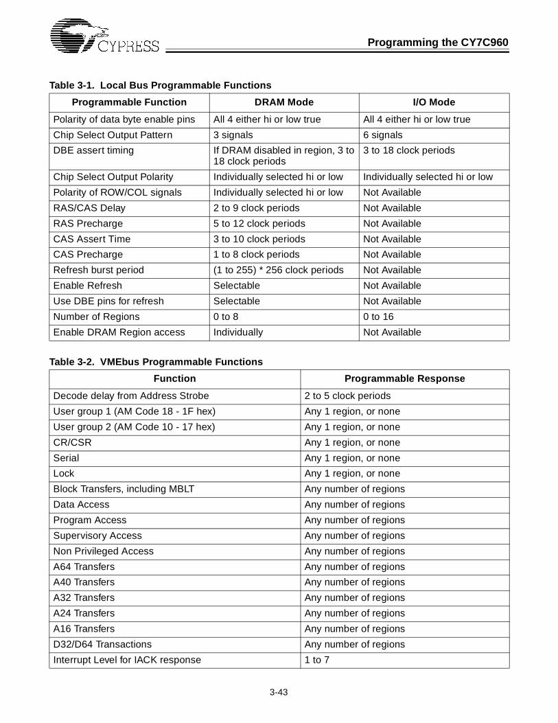
Programming the CY7C960
3-43
Table 3-1. Local Bus Programmable Functions
Table 3-2. VMEbus Programmable Functions
Programmable Function DRAM Mode I/O Mode
Polarity of data byte enable pins All 4 either hi or low true All 4 either hi or low true
Chip Select Output Pattern 3 signals 6 signals
DBE assert timing If DRAM disabled in region, 3 to 18 clock periods
3 to 18 clock periods
Chip Select Output Polarity Individually selected hi or low Individually selected hi or low
Polarity of ROW/COL signals Individually selected hi or low Not Available
RAS/CAS Delay 2 to 9 clock periods Not Available
RAS Precharge 5 to 12 clock periods Not Available
CAS Assert Time 3 to 10 clock periods Not Available
CAS Precharge 1 to 8 clock periods Not Available
Refresh burst period (1 to 255) * 256 clock periods Not Available
Enable Refresh Selectable Not Available
Use DBE pins for refresh Selectable Not Available
Number of Regions 0 to 8 0 to 16
Enable DRAM Region access Individually Not Available
Function Programmable Response
Decode delay from Address Strobe 2 to 5 clock periods
User group 1 (AM Code 18 - 1F hex) Any 1 region, or none
User group 2 (AM Code 10 - 17 hex) Any 1 region, or none
CR/CSR Any 1 region, or none
Serial Any 1 region, or none
Lock Any 1 region, or none
Block Transfers, including MBLT Any number of regions
Data Access Any number of regions
Program Access Any number of regions
Supervisory Access Any number of regions
Non Privileged Access Any number of regions
A64 Transfers Any number of regions
A40 Transfers Any number of regions
A32 Transfers Any number of regions
A24 Transfers Any number of regions
A16 Transfers Any number of regions
D32/D64 Transactions Any number of regions
Interrupt Level for IACK response 1 to 7
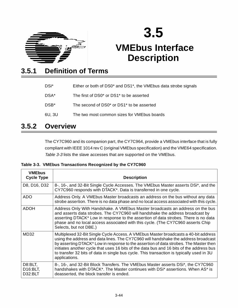
3-44
3.5 VMEbus Interface
Description3.5.1 Definition of Terms
DSi* Either or both of DS0* and DS1*, the VMEbus data strobe signals
DSA* The first of DS0* or DS1* to be asserted
DSB* The second of DS0* or DS1* to be asserted
6U, 3U The two most common sizes for VMEbus boards
3.5.2 Overview
The CY7C960 and its companion part, the CY7C964, provide a VMEbus interface that is fully
compliant with IEEE 1014 rev C (original VMEbus specification) and the VME64 specification.
Table 3-3 lists the slave accesses that are supported on the VMEbus.
Table 3-3. VMEbus Transactions Recognized by the CY7C960
VMEbus Cycle Type Description
D8, D16, D32 8-, 16-, and 32-Bit Single Cycle Accesses. The VMEbus Master asserts DSi*, and the CY7C960 responds with DTACK*. Data is transferred in one cycle.
ADO Address Only. A VMEbus Master broadcasts an address on the bus without any data strobe assertion. There is no data phase and no local access associated with this cycle.
ADOH Address Only With Handshake. A VMEbus Master broadcasts an address on the bus and asserts data strobes. The CY7C960 will handshake the address broadcast by asserting DTACK* Low in response to the assertion of data strobes. There is no data phase and no local access associated with this cycle. (The CY7C960 asserts Chip Selects, but not DBE.)
MD32 Multiplexed 32-Bit Single Cycle Access. A VMEbus Master broadcasts a 40-bit address using the address and data lines. The CY7C960 will handshake the address broadcast by asserting DTACK* Low in response to the assertion of data strobes. The Master then initiates another cycle that uses 16 bits of the data bus and 16 bits of the address bus to transfer 32 bits of data in single bus cycle. This transaction is typically used in 3U applications.
D8:BLT, D16:BLT, D32:BLT
8-, 16-, and 32-Bit Block Transfers. The VMEbus Master asserts DSi*, the CY7C960 handshakes with DTACK*. The Master continues with DSi* assertions. When AS* is deasserted, the block transfer is ended.

VMEbus Interface Description
3-45
MD32:BLT Multiplexed 32-Bit Block Transfer. A VMEbus Master broadcasts a 40-bit address using the address and data lines. The CY7C960 will handshake the address broadcast by asserting DTACK* Low in response to the assertion of data strobes. The Master then initiates a series of cycles that use 16 bits of the data bus and 16 bits of the address bus to transfer 32 bits of data in each cycle of the burst. This transaction is typically used in 3U applications.
D64:MBLT Multiplexed 64-Bit Block Transfer. A VMEbus Master broadcasts a 32- or 24-bit address on the address lines or a 64-bit address on the address and data lines. The CY7C960 will handshake the address broadcast by asserting DTACK* Low in response to the assertion of data strobes. The Master then initiates a series of cycles that use 32 bits of the data bus and 32 bits of the address bus to transfer 64 bits of data in each cycle of the burst. When AS* is deasserted, the block transfer is ended.
D8:RMW, D16:RMW, D32:RMW
8-, 16-, and 32-Bit Read-Modify-Write Cycles. A VMEbus Master reads data from the slave board, modifies that data, and writes it back to the board in a single transaction. The CY7C960 provides DTACK* in response to each DSi* assertion.
MD32:RMW Multiplexed 32-Bit Read-Modify-Write. A VMEbus Master broadcasts a 40-bit address using the address and data lines. The CY7C960 will handshake the address broadcast by asserting DTACK* Low in response to the assertion of data strobes. The Master then initiates a cycle that reads 16 bits of the data bus and 16 bits of the address bus, modifies that data, and writes the data back in a single VMEbus access. This transaction is typically used in 3U applications. The CY7C960 provides DTACK* in response to each DSi* assertion.
D32:UAT 32 Bit Unaligned Transfer. A VMEbus Master transfers 16 or 24 bits of data using a single cycle access. For example, a Master may transfer 16 bits of data using VMEbus data Byte 1 and Byte 2. The CY7C960 provides DTACK* in response to the DSi* asser-tion.
A16, A24, A32, A40, A64
The CY7960 can be programmed to respond to any of the address-based AM codes.
CR/CSR Configuration ROM/Control and Status Register accesses. The CY7C960 can be pro-grammed to respond to this AM Code.
SERIAL Serial cycles. The extension to the VMEbus specification defines the use of certain reserved AM Codes for this serial data interface. The CY7C960 can be programmed to respond to these AM Codes.
LOCK LOCK cycles. The CY7C960 provides limited support by acknowledging the address broadcast from the VMEbus Master. No local signals are driven. The CY7C961 device provides a complete LOCK facility.
USER 16 VMEbus AM codes grouped as USER1(18–1F) and USER2 (10–17). The CY7C960 can be programmed to respond to these transactions.
IACK The VMEbus Interrupt Handler provides an IACK cycle in response to a VMEbus inter-rupt. The CY7C960 responds to IACK cycles as appropriate.
Table 3-3. VMEbus Transactions Recognized by the CY7C960 (continued)
VMEbus Cycle Type Description

VMEbus Interface Description
3-46
There are many features of the CY7C960 interface solution which can be combined in variousways and augmented with external decoder logic to configure a slave board to respond in anyof 16 VMEbus address regions. The CY7C960 can be programmed to respond to a subsetof the transaction types listed in Table 3-3 when they occur within user-specified regions ofVMEbus address space. (Refer to Programming the CY7C960 for complete details on howto configure the device.) This section will describe how the CY7C960 uses its AM codeprogramming and REGION inputs to respond to certain transactions within certain addressregions and how the CY7C960 is selected by a Master. As the CY7C960 is designed to handlethe complexity of the VMEbus transaction processing without external assistance, it is notnecessary to understand the internal circuitry to any great extent. The following two sectionsprovide the basic knowledge needed to use the device: the rest of the chapter can be viewedas reference material.
3.5.3 Region Mapping
The CY7C960 receives VMEbus address decoder information on its REGION inputs. Slaveselection begins by decoding these inputs. There are four REGION inputs available when theCY7C960 is configured as an IO controller and three REGION inputs when it is configuredas a combination DRAM/IO controller. Refer to the Local Interface Description for details onthese configurations. The IO controller configuration will be assumed for the purpose of thisdiscussion.
The purpose for providing this large number of Regions is to allow a board to respond differ-ently to the various VMEbus transactions that can be enabled. Each Region can have its own“personality.” For example some respond to block transfers, some do not. One or more of the16 decoded Regions can be designated as the “unselected” regions. The way this is done isdescribed in the next section.
The CY7C964s are configured to drive the VME address onto the local address bus. VMEbusaddresses flow through and allow external decode logic to take advantage of the VMEbusbuffering provided by the CY7C964 transceivers. In the case of A64 and A40 transactions,the CY7C960 provides two signals, DENIN* and DENIN1*, which can be used to instruct theexternal decoder circuitry when to sample the VMEbus data signals (available on the localdata bus, buffered by the CY7C964 devices) for this multiplexed address information. Thus,the user may choose to implement a comparator externally of any complexity and drive theREGION inputs from this external circuit.
The amount of time the CY7C960 waits before sampling the REGION inputs is specifiedduring initialization. The parameter is called Decode Delay. The CY7C960 starts counting thenumber of clocks that occur from the assertion of AS* by the VMEbus Master. When thenumber of clocks equal the Decode Delay, the CY7C960 samples the four REGION inputs todetermine which one of 16 possible address regions the cycle is directed towards.
Decode delay starts with the sampling of DSB* instead of AS* in the case of multiplexedaddress cycles such as A64. This is to allow address information to arrive on the VME data bus.
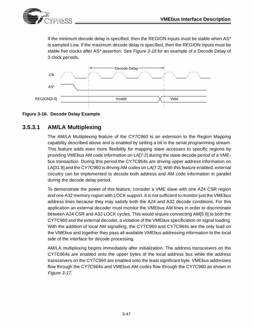
VMEbus Interface Description
3-47
If the minimum decode delay is specified, then the REGION inputs must be stable when AS*is sampled Low. If the maximum decode delay is specified, then the REGION inputs must bestable five clocks after AS* assertion. See Figure 3-16 for an example of a Decode Delay of3 clock periods.
Figure 3-16. Decode Delay Example
3.5.3.1 AM/LA Multiplexing
The AM/LA Multiplexing feature of the CY7C960 is an extension to the Region Mappingcapability described above and is enabled by setting a bit in the serial programming stream.This feature adds even more flexibility for mapping slave accesses to specific regions byproviding VMEbus AM code information on LA[7:2] during the slave decode period of a VME-bus transaction. During this period the CY7C964s are driving upper address information onLA[31:8] and the CY7C960 is driving AM codes on LA[7:2]. With this feature enabled, externalcircuitry can be implemented to decode both address and AM code information in parallelduring the decode delay period.
To demonstrate the power of this feature, consider a VME slave with one A24 CSR regionand one A32 memory region with LOCK support. It is not sufficient to monitor just the VMEbusaddress lines because they may satisfy both the A24 and A32 decode conditions. For thisapplication an external decoder must monitor the VMEbus AM lines in order to discriminatebetween A24 CSR and A32 LOCK cycles. This would require connecting AM[5:0] to both theCY7C960 and the external decoder, a violation of the VMEbus specification on signal loading.With the addition of local AM signalling, the CY7C960 and CY7C964s are the only load onthe VMEbus and together they pass all available VMEbus addressing information to the localside of the interface for decode processing.
AM/LA multiplexing begins immediately after initialization. The address transceivers on theCY7C964s are enabled onto the upper bytes of the local address bus while the addresstransceivers on the CY7C960 are enabled onto the least significant byte. VMEbus addressesflow through the CY7C964s and VMEbus AM codes flow through the CY7C960 as shown inFigure 3-17.
ValidInvalid
AS*
Clk
REGION[3:0]
Decode Delay

VMEbus Interface Description
3-48
Figure 3-17. AM/LA Multiplexing with Decode Delay = 2T
The assertion of LADI is the event used to latch the local AM codes presented on LA[7:2]within an external decoder. The CY7C960 local address transceivers are disabled and theCY7C964 local address transceivers are enabled one clock after LADI assertion. The VMEbussignals A[7:1] and LWORD* will flow through to LA[7:0] of the least significant CY7C964 atthis time. The CY7C960 then stores the values presented to it on LA[1] and LWORD* tocomplete the slave decode process. These values are used to compute the correct data byteenable pattern during the data phase of the access.
Figure 3-18 shows the effect of introducing Decode Delay to the address phase of a slaveaccess when AM/LA Multiplexing is enabled. The timing of AS* sampling, LADI assertion,and local address bus transition from AM[5:0] to LA[7:1] and LWORD* remain the same asin Figure 3-17 while the duration of LA[7:1], LWORD*, and the time to valid chip selects willincrease according the number of Decode Delay clocks programmed at initialization.
Figure 3-19 represents the same slave access as in Figure 3-17 except that AM/LA multiplex-ing is turned off. In this case, all four CY7C964s are enabled onto the local bus while theCY7C960 is waiting to be accessed by a Master. The CY7C960 will not drive the local addressbus until the second and subsequent beats of a Block Transfer.
VALID AM CODE
AM[5:0]
VALID
CY7C964 drives LA[7:1] CY7C960 Drives
VALID
AM
AS*
LADI
CS
LAEN
LA[7:0]
LA[31:8]
REGION
DBE
CLK

VMEbus Interface Description
3-49
Figure 3-18. AM/LA Multiplexing with Decode Delay = 5T
Figure 3-19. AM/LA Multiplexing Disabled with Decode Delay = 2T
VALID AM CODE
AM[5:0]
VALID
CY7C964 drives LA[7:1]
VALID
CY7C960 Drives
AM
AS*
LADI
CS
LAEN
LA[7:0]
LA[31:8]
REGION
DBE
CLK
VALID AM CODE
VALID
CY7C960 Drives
VALID
CY7C964 Drives LA[7:1]
AM
AS*
LADI
CS
LAEN
LA[7:0]
LA[31:8]
REGION
DBE
CLK
VMEbus Interface Description
3-50
3.5.4 Bus Holdoff
The Bus Holdoff feature of the CY7C960 provides the ability to three-state the slave interfacechip set (CY7C960 and CY7C964s) and suspend slave decode activity in order to easily dual-port devices mapped as VMEbus slave resources. This feature also extends the functionalityof the CY7C961 by allowing local configuration of its master DMA channel. The feature isenabled by setting a bit in the serial programming stream.
The mechanism for Bus Holdoff is overlaid on the CY7C960 LACK pin. When Bus Holdoff isenabled, LACK acquires a local bus grant function in addition to its previously described localtransaction acknowledge function. By controlling LACK deassertion, it is possible to suspendall local response of the slave interface chip set, effectively delaying the next VMEbus slaveaccess until LACK is reasserted.
While the CY7C960 is in its holdoff state, output signals DBE, RW, CS, and LA are three-state, and control signals DENIN[1:0]* and LAEN three-state the LD and LA pins of the leastsignificant CY7C964 device. LAEN on the most significant CY7C964s must also be externallycontrolled during Bus Holdoff. This holdoff configuration is intended to allow simple design ofaddress, data, and control multiplexing to achieve dual-ported local memory architectures.
The CY7C960 Bus Holdoff feature conceptually allows cycle stealing by other local bus mas-ters. This is accomplished by using an output of the CY7C960, the LADI signal, as an interfacebusy signal. A local bus arbiter can monitor LADI and deassert LACK within two clocks aftera deassertion edge on LADI. LADI deassertion represents the end of a VMEbus transactionregardless of whether it was decoded by the CY7C960 interface. If LACK is deasserted inthe bus holdoff window, the local bus is three-state until LACK is again asserted. If LACK isdeasserted outside the holdoff window, LACK performs its local acknowledge function.
3.5.4.1 Transaction Type Detection
There is another internal decoder: the CY7C960 decodes AM[5:0] and forms an internalAddress Modifier Decode Word after the same Decode Delay interval that is used for samplingthe REGION inputs. As the VMEbus specification dictates that AM Codes be stable prior tothe assertion of AS* then the Decode Delay is unnecessary, but is used for convenience.
Two fields result from decoding the AM Codes: Address Size and Modifiers. Table 3-4 providesa definition of the CY7C960’s classification of AM Codes.

VMEbus Interface Description
3-51
Figure 3-20. Local Bus Holdoff
r
Table 3-4. AM Code Decode
Address Size Modifier VMEbus Transactions
A64 A64 block transfer (BLT); A64 single cycle access; A64 64-bit block transfer (MBLT); A64 lock command (LCK); A64 serial access
A40 A40 block transfer (BLT); A40 single cycle access; A40 lock command (LCK); A40 serial access
A32 A32 supervisory block transfer (BLT); A32 supervisory program access; A32 su-pervisory data access; A32 supervisory 64-bit block transfer (MBLT); A32 non-privileged block transfer (BLT); A32 non-privileged program access; A32 non-privileged data access; A32 non-privileged 64-bit block transfer (MBLT); A32 lock command (LCK); A32 serial access
A24 A24 supervisory block transfer (BLT); A24 supervisory program access; A24 su-pervisory data access; A24 supervisory 64-bit block transfer (MBLT); A24 non-privileged block transfer (BLT); A24 non-privileged program access; A24 non-privileged data access; A24 non-privileged 64-bit block transfer (MBLT); A24 lock command (LCK); A24 serial access
A16 A16 supervisory access; A16 non privileged access; A16 lock command (LCK); A16 serial access
SUPER Supervisory access
NPRIV Non-Privileged access
PROG Program access
BLT Block transfer (inc. MBLT)
LONG 32 or 64 bit access (not 8 or 16)
LOCK A64 lock command (LCK), A40 lock command (LCK), A32 lock command (LCK), A24 lock command (LCK), A16 lock command (LCK)
SERIAL A64 serial, A40 serial, A32 serial, A24 serial, A16 serial
CR/CSR Configuration ROM/Control and Status Register
U1, U2 User Defined (U1 includes AM Codes 18–1F, U2 includes 10–17)
CLK
LACK
LADI
RW
LAEN
LA
LD
DENIN
DBE
CS

VMEbus Interface Description
3-52
It should be noted that the parameter LONG is derived from a combination of DSi*, LWORD*,and AM Code. For more information on AM Code definitions, it is recommended that theVMEbus Specification be consulted.
The reason that the CY7C960 decodes the AM Code this way is to allow the user to enableVMEbus transactions selectively by AM Code classification. For example, a transaction withAM Code “0C” would result in the following settings: A32, SUPER, BLT, LONG. The CY7C960would react to the transaction only if all four categories were enabled for the addressed Region.The CY7C960 consults a look-up table, configured during initialization, to determine whetherthe transaction is enabled or not. Table 3-5 is an example of how this table could be pro-grammed.
Table 3-5. Major AM-to-Region Mapping Example
If the CY7C960 is configured according the table above, then it will respond as slave underthe following conditions.
If the REGION inputs are “0000”, then the CY7C960 will respond to A64 block transfers oftype BLT or MBLT.
If the REGION inputs are “0001”, then the CY7C960 will respond to A40 block transfers oftype D8:BLT, D16:BLT, or MD32:BLT.
If the REGION inputs are “0010”, then the CY7C960 will respond to A32 supervisory programaccesses of type D8, D16, or D32 (single cycle).
If the REGION inputs are “0011”, then the CY7C960 will respond to A24 non-privileged dataaccesses of type D8, D16, or D32 (single cycle).
REGION A64 A40 A32 A24 A16 SUPER NPRIV PROG DATA BLT LONG
0
1
2
3
4
5
6
7
8
9
10
11
12
13
14
15

VMEbus Interface Description
3-53
If the REGION inputs are “0100”, then the CY7C960 will respond to A24 supervisory program,and A16 supervisory accesses of type D8 or D16 (single cycle). Note that D32s will not beresponded to in this region because LONG is not set.
If the REGION inputs are “0101”, then the CY7C960 will respond to any A32 AM Code otherthan A32 LOCK and A32 SERIAL which must be enabled separately (see below).
If the REGION inputs are any other value, then the CY7C960 will assume that the cycle isintended for another board and will not respond.
LOCK, SERIAL, USER, and CR/CSR AM codes are treated somewhat differently from the“mainstream” codes. Each of these codes can be assigned to only a single specific REGION.Since these transactions are typically mapped to a single address space on a board, it wasnot necessary to include them in all 16 rows of the main REGION/AM decode lookup table.The user simply selects which, if any, of these transactions should be decoded and assignsa valid REGION pattern to them.
Table 3-6 shows an example: A32 LOCK transactions are enabled in Region 0; A40 and A16SERIAL transactions are enabled in Region 8; User AM codes in group 1 are enabled inRegion 10; the remaining two classifications are disabled (but had they been enabled theywould have been enabled for Region 2).
Table 3-6. Minor AM-to-Region Mapping Example
If the VMEbus transaction is determined by the above process to be enabled for the Regionbeing addressed, then the CY7C960 internal flag DECODE is set, allowing local activity tocommence. Figure 3-21 shows a flowchart representation of the process of decoding a VME-bus Transaction.
A slave board that uses the CY7C960 can be programmed to respond in a wide variety ofways with a fine control on decode granularity by using the CY7C960’s Region Mappingfeatures. The following sections and the AC timing diagrams at the end of this document areintended for users who need to know further details of the features described above.
AM Classification A64 A40 A32 A24 A16 Enable Region
LOCK 0
SERIAL 8
USER1 (AM Codes 18 - 1F)
These do not have an associated address size
10
USER2 (AM Codes 10 - 17)
2
CR/CSR 2

VMEbus Interface Description
3-54
Figure 3-21. Flowchart for Decoding VMEbus Transactions
3.5.5 Decode Delay Timing
Slave decode delay timing is a process that conceptually begins whenever AS* is sampledlow on the rising edge of CLK. However, at this time the CY7C960 slave decoder must waitfor all local activity to clear before processing a VMEbus cycle. This is because it is possiblefor a local cycle to be in progress without a Master on the VMEbus.
For example, in the case of a posted slave write, the VMEbus Master is allowed to leave thebus with data still to be processed in the interface. If this is the case, then the local addressbus will be holding an address from this posted write. Likewise, there are situations wherethe CY7C960 will perform a read-ahead cycle. This happens when block transfer reads donot terminate on a 256-byte boundary. The on-board slave decoder must wait for this address
Decode REGION & AMCode Inputs
Is Address Sizeenabled for Region
CR/CSR or
Yes
No
No
Are ModifiersEnabled for Region
Yes
Yes
Successful Decode
Yes
No
AS* LOW andDecode Delay
ExpiredNo
Start
User-AM

VMEbus Interface Description
3-55
to clear and allow enough time for the new address to arrive and become stable on the localbus.
The internal AM decoder then signals whether the first cycle will be an address broadcastcycle. Since MBLT and MD32 transactions use the address bus for data transfers, a Masterinitiating these transactions will first issue an address broadcast so the Slave can capture thestarting address before the address bus changes into a data transfer bus. This addressbroadcast cycle also occurs for transactions that use the VME data bus as an address bus.These cycles include all A64 and A40 transactions since the width of the VME address busis only 32 bits (24 bits for 3U boards).
If there will be no address broadcast cycle, then the decode delay timeout begins with AS*.An internal timer counts up to the programmed decode delay. If an address broadcast cycleis signalled, then the CY7C960 will wait for the DSB* event and then count up to the pro-grammed decode delay.
In either case, after the decode delay has expired, the CY7C960 will determine if the address-ing information for this cycle falls with its programmed address space. If it does, then aninternal flag signals other internal circuitry that the cycle is a valid slave decode for the board.If it does not, then the internal slave decoder will wait until AS* is sampled High and thenreturn to an idling state waiting for the next VMEbus cycle.
3.5.6 Slave Addressing Before Initialization
The CY7C960 can be programmed in one of three ways. The interface can be programmedfrom the VMEbus, the local bus, or a combination of the VME and local buses. If the CY7C960is programmed using the VMEbus or the combination method, slave address information anddevice programming is loaded using a methodology compliant with the VMEbus Auto Slot IDspecification using either a CR/CSR or A16 AM code. The configuration ROM/control andstatus register (CR/CSR) capability described by the latest revision of the VMEbus specifica-tion provide a mechanism for board identification and automatic initialization. Auto Slot ID isan optional method of assigning the CR/CSR base address to each VMEbus board. This AutoID slave uses a level 2, D8 interrupter along with additional board specific hardware to obtainthe CR/CSR base address. An Auto ID Master, called the Monarch, uses a level 2, D8 InterruptHandler to acknowledge the Auto ID interrupt and assigns a base address to the slave board.Specifically, this Auto ID slave:
1. generates a level 2 interrupt if PDATA is sampled Low after power-on or a negative edgeon SYSRESET*. (IRQ* must be connected to IRQ[2]* on the VMEbus.)
2. waits for and responds to the level 2 IACK cycle initiated by the Monarch.
3. asserts LDEN* thereby enabling a Status/ID byte that is sourced by external local hard-ware.
4. presents the Status/ID byte on the VMEbus. (all 32 bits of VMEbus data are driven)

VMEbus Interface Description
3-56
5. drives DTACK* Low and releases IRQ*.
The Monarch must then:
1. write the base address of this board using a single cycle write with a CR/CSR or A16 AMcode. If a CR/CSR AM code is used, then all subsequent programming cycles must usea CR/CSR AM code. Likewise, if an A16 AM code is used, then all subsequent program-ming cycles must use an A16 AM code. It is mandatory that this access be indivisible withthe previous IACK cycle on the backplane to avoid collisions with
2. program the CY7C960 internal registers using a series of single-cycle writes to the base
address of the slave if the VMEbus Initialization Method is used. These accesses require
a bit pattern of ‘xx00’ on REGION[2:0] if a CR/CSR AM code is used and ‘xxx0’ if an A16
AM code is used.
3. initialize the CY7C964 compare and mask registers using two single writes to the base
address of the slave. These two writes will reassign the CR/CSR base address of the
slave to its new base address in the system.
3.5.7 Address and Data Strobe Event Processing
Another process begins in parallel with slave decoding. The following sequence of eventsoccurs whenever AS* is sampled Low by the CY7C960:
• The internal AM decoder signals whether the first cycle will be an address broadcastcycle. Since MBLT and MD32 transactions use the address bus for data transfers, a Masterinitiating these transactions will first issue an address broadcast cycle so the Slave cancapture the starting address before the address bus changes into a data transfer bus.This address broadcast cycle also occurs for transactions that use the VME data bus asan address bus. These cycles include all A64 and A40 transactions since the width of theVME address bus is only 32 bits.
• The value of LWORD* is latched and held for the duration of the transaction. LWORD* onthe VMEbus must be connected to A[0] on the least significant CY7C964 becauseLWORD* is captured by the CY7C960 on LA[0]. This does not present a problem becauseA[0] on the VMEbus is encoded on the VMEbus data strobes.
• The local address that has been flowing through the CY7C964s will now be latched. Animportant consideration to note here is that the transaction may be intended for anotherslave on the backplane and that slave may respond very quickly on its DTACK* or BERR*lines. Since the Master is permitted to remove the address after the responding Slavedrives DTACK* or BERR* Low, the CY7C960 will signal the CY7C964 to latch its localaddress lines at this time in order to capture the addressing information before it can beremoved. This is accomplished by the assertion of LADI from the CY7C960 to theCY7C964.

VMEbus Interface Description
3-57
The CY7C960 then waits for the DSB* and DECODE events. The DSB* event is defined bythe VMEbus specification, which states that maximum skew between the assertions DS1*and DS0* Low by a Master shall be no more than 20 ns at the Slave. When the CY7C960samples either DS1* or DS0* Low by CLK, it waits two clocks and then sets an internal flagcalled DSB*. This two clock waiting period is designed to accommodate any data strobe skewwithin specification by ensuring that both strobes have had time to arrive before the devicedecodes addressing information from the strobes.
The DECODE event is another internal flag that is set ‘true’ or ‘false’ depending on whetherthe CY7C960 has been selected. Refer to the previous sections on slave address decodingfor a description of this process.
Several things happen when these two events occur. Data size information is decoded fromthe values on DS1*, DS0*, LA[1], and LWORD*. This information is used to determine localbyte enable patterns (DBE[3:0]), data byte swapping control (SWDEN*), and local addresscounting. The CY7C960 also disables the drivers on the least significant CY7C964 and beginsto drive the starting address for the transaction on LA[7:0].
If either of these two events fail to occur, then the CY7C960 will wait until it samples AS* High,deassert LADI thereby letting VME address flow through to local address on the CY7C964’s,and return to an idling state waiting for the next AS* Low event.
3.5.8 Slave Data Transfer Acknowledgment
Slave data transfers are acknowledged by a Low assertion of the DTACK* output. All asser-tions of DTACK* require the assertion of the internal DECODE and DSB* flags. If these twoconditions are present, then DTACK* will be asserted Low on the backplane when
• the internal AM decoder signals that an address broadcast cycle is in progress. Addressbroadcast cycles do not generate local chip selects.
• the cycle is a slave read of any type. The CY7C960 will assert DTACK* Low when its localcontroller sets an internal flag that indicates data has been read from the local board andthe data is being held in the interface (CY7C964s).
• the cycle is a slave block transfer write of any type. This is the case where data is postedin the interface and the VMEbus Master is allowed to start the next cycle or terminate thetransaction. While the Master is starting the next cycle or terminating, the CY7C960 localcontroller writes the posted data to the local board. Slave write posting of block transfercycles allow the CY7C960 to transfer data at a maximum rate of 80 Mbytes/s for MBLTbursts and 40 Mbytes/s for BLT bursts.
• the cycle is a single-cycle slave write of any type and the CY7C960 local controller hasfinished writing the data to the local board. This is the case where data is not posted inthe interface and the VMEbus Master must wait for the write transfer to complete beforestarting the next cycle or terminating.

VMEbus Interface Description
3-58
3.5.9 Slave Write Posting
Slave write posting is a means of obtaining maximum data transfer performance by decouplingthe VMEbus from the local board. Every slave write data transaction is latched in theCY7C964s for further processing by the CY7C960 local controller and the VMEbus Masteris allowed to begin its next cycle or terminate the transaction.
In other words, the VMEbus Master drives DSi*, and the CY7C960 drives DTACK* before thedata has reached the local bus.
Data is latched in the interface when DSB* occurs during a slave write to a valid addressregion. At this time the CY7C960’s local controller initiates a write cycle to the local board.This pipelined architecture allows fast VMEbus cycles that are not delayed by local affectssuch as DRAM refresh bursts, or resource contention. When the local cycle is complete, thedata latches are opened and new data is allowed to flow into the interface. Also, LA[7:0] isincremented according to the data width of the transaction after the local board acknowledgesthat the posted data has been written.
3.5.10 Slave Read-Ahead Cycles
Slave read-ahead cycles are also used to achieve maximum data transfer rates for blocktransfer reads. When the CY7C960 completes a read cycle to a VMEbus Master during ablock transfer operation, it will read ahead on the local bus in order to have data ready for thenext cycle of the burst.
Data is read from the local board, latched in the interface, and driven on the VMEbus datalines when DSB* arrives to start a slave block transfer read from a valid address region. Notethat all 32 bits of data are driven on the VMEbus data lines, regardless of data size. TheCY7C960 asserts DTACK* Low to signal that the data is ready to be taken. When the VMEbusMaster releases the data strobes, the CY7C960 stops driving the VMEbus data lines andLA[7:0] are incremented according to the data width of the transaction. The CY7C960 thenperforms another local read in preparation for the next cycle of the read burst.
Since there is no indication to the slave as to how long a block transfer will be or when it willterminate, it is possible to have a read-ahead cycle occur that does not get transferred to theMaster. In other words, the Master could terminate before, during, or after the read-aheadand the local data that was read would not be transferred to the VMEbus. However, theCY7C960 will not read ahead at a 256 byte boundary even if 2k byte boundaries are in effectas is the case for some MBLT transactions. The read circuitry was implemented this way inorder to provide a means of averting read-ahead cycles and is possible because the CY7C960drives LA[7:0], which enables it to detect when the address is about to overflow.
Also, as in the case of MBLT and MD32 transactions, there can be two local accesses to beprocessed for one VMEbus access. The CY7C960 handles all the pipelining and multiplexing

VMEbus Interface Description
3-59
control that must take place in the interface to accommodate reads or writes when the VMEdata bus is wider than the local data bus.
3.5.11 Interrupt Cycle Support
There are six pins associated with interrupt requesting on the VMEbus: IRQ*, IACK*, IACKIN*,IACKOUT*, LDEN*, and LIRQ*. There are two ways an interrupt can be signalled on theVMEbus backplane: a local interrupt request or a reset.
A power-on, system reset, or local reset condition causes the device to implement its initial-ization protocol. Refer to sections 3.4.3 and 3.4.5 for details on initialization.
LIRQ* is the input to the device from local circuitry demanding an interrupt cycle. If the LIRQ*signal is asserted Low, the CY7C960’s IRQ* pin is asserted Low. The local circuitry shouldremove LIRQ* after the interrupt has been acknowledged: The CY7C960 simply drives thestate of LIRQ* onto IRQ*. Figure 3-22 illustrates the relationship between LIRQ* and IRQ*.s60 represents the assert and deassert delays.
Figure 3-22. Interrupt Signal Timing
The CY7C960 actively drives the value of IACKIN* to IACKOUT* in conformance with therules for VMEbus D8 Interrupt Acknowledge Cycles. If it is driving IRQ* and IACK* is sampledLow and IACKIN* is sampled Low and AS* is sampled Low, then LA[3:1] is compared withthe programmed interrupt request level. If they are not equal then the Low IACKIN* is drivento IACKOUT*. If they are equal, then IACKOUT* remains High and LDEN* is driven Low toenable an external Status/ID vector onto the local data bus. This vector is in turn enabled ontothe backplane and the VMEbus Interrupt Handler is acknowledged by a Low transition on theDTACK* line.
It is important to note that, while the CY7C960 is a D8 interrupter, it drives all 32 bits of VMEbusdata on the backplane with the assertion of DENO* to the CY7C964s. If the user wishes toprovide only 8 bits of status ID, then the value of the upper bytes should be set to FF hex toensure full compliance with the VMEbus specification. If the user wishes to provide 16 or 32bits of status ID, then the interrupt handler should be programmed to handle the providedwidth. The CY7C960 does not attempt to differentiate between 8-, 16-, or 32-bit interruptacknowledge cycles.
IRQ*
LIRQ
s60 s60
VMEbus Interface Description
3-60
3.5.12 Interrupt Handshake Support
The CY7C960 can be programmed at initialization to wait for a local acknowledge signalbefore terminating an IACK cycle. LACK is the local signal used to suspend completion of anIACK cycle until the local interrupter is ready to present a STATUS/ID vector to the VMEbusInterrupt Handler.
If the Handshake bit is set the CY7C960 will sample the state of the LACK pin three clocksafter it samples a Low level on its IACKIN* pin during a VMEbus IACK cycle. If LACK is Highat this time, then the CY7C960 will wait until LACK is Low before terminating the cycle witha falling edge on DTACK*.
If the Handshake bit is not set, the CY7C960 will ignore the state of the LACK pin and DTACK*the VMEbus Interrupt Handler four clocks after sampling a valid IACKIN*.
Handshake support is available immediately after local completion of the Combination Initial-ization Method or after full completion of the VMEbus or Local Initialization Methods. Referto Chapter 3.4 for details on the three programming methods.
3-61
3.6CY7C964 Interface
3.6.1 CY7C964 Overview
The CY7C960 is designed for use with the CY7C964 VMEbus Interface Logic Circuit. Thisdevice is fully described in Section 4, The CY7C964 Bus Interface Logic Circuit. The CY7C960provides all the control and timing for the interface with the CY7C964. Interface timing asgenerated by the CY7C960 is designed for CY7C964 delay characteristics.
The CY7C964 contains a collection of counters, latches, and multiplexers used to facilitatedata handling during any of the many VMEbus data transactions. Three-state high drivebuffers allow direct connection to VME and local address and data busses. Additionally, theCY7C964 contains an address comparator with mask function to allow the CY7C964 to formpart of the user’s slave address decoder. Defined as a companion to the VIC068A/VIC64devices, the CY7C964 has been designed into many high-performance VME64 CPU boards.In concert with the CY7C960, it performs the functions of address decoder, D64 data multi-plexer, and local address counter, to facilitate the design of high-performance slave systems.
3.6.2 CY7C964 Connections
The signals that are provided by the CY7C960 for use by the CY7C964 are: LADI, LEDI,LEDO, DENO*, ABEN*, DENIN*, DENIN1*, LAEN, STROBE, LDS, and D64 using dedicatedpins. These signals are described in the pin description section.
LADI (Latch ADdress In) controls a transparent latch which connects the VMEbus addressto the local address. The default state of the signal ensures that the VMEbus address is drivento the local pins, allowing the implementation of VMEbus address decoder circuitry on thelocal address bus. The LAEN (Local Address ENable) input is tied High on all but the leastsignificant CY7C964 to ensure that the local address is always enabled. The least significantCY7C964 has its LAEN pin controlled by the CY7C960 to allow the CY7C960 to source theLSB of address during block transfers when the address has to increment by 1, 2, or 4(dependent on the transfer type: single, double, or quad byte). Note that in order to takeadvantage of the “local bus holdoff” feature of the CY7C960, it is necessary to control LAENof the upper 3 CY7C964 devices. LAEN must be driven Low during holdoff.
LEDI (Latch Enable Data In) and LEDO (Latch Enable Data Out) control the VMEbus andlocal data transfer latches in the CY7C964. Data read from local resources must be set upto LEDO for burst transfers, while LEDI provides data hold time during burst transfers whendata is captured from the CY7C964. These signals, by holding data in the interface allow“write posting” and “read-ahead” performance features.

CY7C964 Interface
3-62
DENO* (VMEbus Data ENable Out) and the pair of signals, DENIN* and DENIN1* (local DataENable IN) are normally used for local and VMEbus data enable. DENIN* and DENIN1* arealso active during address broadcast of A64 and A40 VMEbus transactions. They are usedto inform an external address decoder when the data bus can be sampled for the high-orderaddress information.
During D64 and MD32 data cycles, the function of DENO* and DENIN*/DENIN1* are identicalto LEDO and LEDI respectively. A two-stage pipelined latch inside the CY7C964 is controlledin the data sourcing case by LEDO and DENO* working in concert, and in the data capturecase by LEDI and DENIN*/DENIN1* working in concert.
Each VMEbus data cycle is served by two local data cycles. The second cycle for slave readmust set data up to the falling edge of DENO*. For slave write, data hold on the second cycleis provided by the assertion of DENIN* (D64) or DENIN1* (MD32).
LDS is used during D64/MD32 slave write transfers to control the VMEbus address to localdata demultiplexing, and during the initialization period to control the selection of the addressmask and compare registers. During multiplexed slave data capture, LDS is the signal whichcontrols data hold time with respect to the deassertion of CAS* and/or DBE.
ABEN* (VME Address Bus ENable) is active only during multiplexed data transactions toenable the VMEbus address pins during D64 or MD32 transfers.
D64 is the signal that informs the CY7C964s that the data phase of multiplexed data transferis in progress and the on-chip pipelining should be used to multiplex or demultiplex the localdata. The CY7C964 is expressly designed to demultiplex D64 and MD32 VME transactionsto a non-multiplexed 32 bit local data bus.
STROBE is a timing signal used to load the on-chip address mask and compare registers ofthe CY7C964. It can be considered a latch enable signal which latches local data when High.
The on-chip counters of the CY7C964 are used for local address counting during slave D64block transfers if the VMEbus master bursts to 2 Kbyte boundaries. Therefore the counterchains must be enabled by connecting the appropriate carry-out to carry-in pins. The VMEbuscounters of the CY7C964 are not used by the CY7C960.
It is recommended that the following connections be made to ensure correct operation duringthe Reset period: Pull-up resistors attached to ABEN*, DENO*; pull-down resistors attachedto LAEN and LADI. These connections prevent CY7C964 drivers from turning on during thebrief periods of three-state operation during reset.
The CY7C964 has several signals which are not used for slave operations: BLT*, FC1, LADO,and MWB*. LADO and FC1 must be tied Low. BLT* and MWB* must be tied High for correctoperation.
Figure 3-23 shows how the control signals for the CY7C964 are driven during initialization toload the Address Compare and Mask Registers. The significant signals are LDS, which selects

CY7C964 Interface
3-63
which register to load, and STROBE, which actually strobes the data on the local bus into theappropriate register.
Figure 3-23. Example of CY7C964 Control Timing
3.6.3 Swap Buffer Control
The CY7C960 is designed to control the swap buffering necessary for handling D8 and D16VMEbus transactions in combination with 32-bit local memory. Figure 3-24 illustrates howVMEbus byte lanes relate to local memory. Note that the CY7C960 coordinates control ofSWDEN* with DENIN*/DENIN1*. The CY7C964 Byte(0) and Byte(1) drivers are turned offduring slave write transfers when SWDEN* is active. Because DENIN*/DENIN1* are used aslatch control signals during multiplexed data transactions (D64 and MD32) DENIN* signalingto CY7C964 Byte(0) and Byte(1) must be modified by external logic IF (and only IF) and boardis to handle BOTH D64 and A40/MD32 slave write transactions. The required circuitry isshown at the top of the figure below.
COMP. MASK
SYSRESET*
LD
LDEN*
PREN*
PDATA
PCLK
STROBE
LDS

CY7C964 Interface
3-64
Figure 3-24. Swap Buffer Design
BY
TE
(2)
CY
7C96
4
’245
CY
7C96
4C
Y7C
964
CY
7C96
4
BY
TE
(0)
BY
TE
(1)
BY
TE
(2)
BY
TE
(3)
’245
DB
E[3
]D
BE
[2]
DB
E[1
]D
BE
[0]
R/W
*S
WD
EN
*D
EN
IN*
DE
NIN
1*
VM
Ebu
s B
YT
E L
AN
ES
BY
TE
(3)
BY
TE
(0)
BY
TE
(1)
BY
TE
(0)
BY
TE
(1)
Cross-connect DENIN*s on upper bytes!
LO
CA
L M
EM
OR
Y
Additional logic only if MD32 and D64 supported on same board
D64
LDS
DENIN1*Byte(0–1)
DENIN*Byte(0–1)
DENIN1*
DENIN*

3-65
3.7 Interfacing without CY7C964
3.7.1 Reduced Cost, Fewer Features
Many board designs need only simple VMEbus slave interfaces. The CY7C960 used in com-bination with Cypress FCT Logic family devices meets this need perfectly. A complete interfacecan be built using the CY7C960 in combination with industry standard latches, transceivers,and latched transceivers.
This interface supports Rev C VMEbus: A16, A24, A32 D8, D16, D32, D32UAT, RMW, in otherwords, a complete interface excluding the performance and multiplexed address features ofVME64.
Because the CY7C964 was designed as an integrated replacement for a pair of bidirectionaltransceivers controlling address and data in the VMEbus interface, the number and sense ofsignals controlling transceiver function have been preserved in the design of the CY7C960.This makes direct connection and control of discrete devices straightforward.
Figure 3-25 illustrates just such an implementation. One pair of CY74FCT16543T deviceshandles the bidirectional data path while a pair of CY74FCT162373T devices provides forlatching and driving 32 bits of address from the VMEbus to the local side of the interface. Aswap buffer, implemented with a CY74FCT162245T device is optional depending on theVMEbus transactions the slave interface is intended to accept.
The pull-up resistor shown is required to program the polarity of the LAEN output of theCY7C960. LAEN is three-stated at power-on or warm reset. The logic level sensed on LAENduring the first initialization cycle determines the deasserted state of LAEN during normaloperation. In this case, the deasserted state is required to be High.
The FCT543 devices are rated 64 mA sink current and 32 mA source current over commercialtemperature range. The FCT245 and FCT373 devices have balanced 24 mA output drive.
In Figure 3-25 all components are drawn to relative scale assuming the CY7C960 in a 64-pinthin quad flat pack. The FCT Logic devices are depicted in thin shrunk small outline packages.The total footprint area of the interface as shown is only 1.08 sq. in. for the 6 chips. Thiscompares to the slightly larger CY7C960/CY7C964 solution requiring 1.16 sq. in. using 5identical packages. The CY7C961/CY7C964 chip set occupies 1.34 sq. in. All of these inter-face sets have thin package profiles suitable for mounting on the back side of a VMEbusboard without violating mechanical clearance requirements.

Interfacing without CY7C964
3-66
Figure 3-25. VMEbus Interface Implemented with CY7C960 and FCT Logic Family.
VCC
LAEN
LADI
R/W*
SWDEN*
LEDI
CY74FCT162245T
CY
74F
CT
1654
3TC
Y74
FC
T16
543
TC
Y74
FC
T16
237
3TC
Y74
FC
T16
2373
T
VMEbus P2
VMEbus P1
LD[15:0]
LD[31:16]
CY
7C
960
LA[31:2]DENIN1*
DENIN*
LEDO
DENO*
A[2
3:1]
, LW
OR
D*
A[3
1:24
]D
[31:
16]
D[1
5:0]
>10k
VCC
>10k
3-67
3.8 DRAM Control Description
3.8.1 Overview
The CY7C960 contains a high-performance DRAM controller, developed to take advantageof DRAMs operating in Fast Page Mode. By using Fast Page Mode devices, VMEbus MBLTtransfer rates of 80 Mbyte per second are attainable with DRAM RAS*-access times of 70ns. With appropriate buffering on the DRAM address and control signals, 16 Mbytes of DRAMcan be directly accommodated (using 4-Mbit devices). With minimal external decoding logicgenerating multiple RAS*/CAS* signals, larger memory arrays can be controlled. When highercapacity DRAM devices become readily available, the memory arrays increase accordingly.
The CY7C960 is configured by the user to work with local DRAM during the initializationsequence. This configuration determines the function of several pins (RAS*, CAS*, ROW,COL, and REGION3/CS2). RAS* and CAS* provide the well-known address strobe signalsfor the DRAM array, ROW and COL provide address enable signals for strobing the row andcolumn addresses into the DRAM array. If DRAM mode is selected during the configurationsequence, then the REGION3/CS2 pin becomes the CS2 output: 8 regions are available inDRAM mode requiring only three REGION decode inputs.
Figure 3-26 shows an example of the use of the DRAM control signals. ROW enables theupper bits of the local address bus to be latched in the DRAM by RAS*. COL enables thelower address bits to be latched by the use of the Data Byte Enable signals. In the examplechosen, the DBE signals are connected to the CAS* inputs of the DRAMs, and the CY7C960has been programmed to provide refresh timing on the DBE pins (DBE Refresh Enabled)
The LACK input may be used to acknowledge DRAM cycles. If LACK is tied Low, then thecycle is self timed using the programmed values for CAS* assert and CAS* precharge. Theuser may prevent DRAM CAS* bursts by the use of the LACK signal. This is done by main-taining LACK High until the DRAM CAS* burst is to be permitted. Once LACK is driven Lowand CAS* is asserted by the CY7C960, the DRAM access is no longer affected by LACK untilRAS* deasserts, signaling the end of the current access (useful in dual-port applications tohold off VMEbus accesses to DRAM).

DRAM Control Description
3-68
Figure 3-26. DRAM Signal Usage
3.8.2 Types of DRAM
The CY7C960 controls Fast Page Mode DRAMs. This is an industry standard mode of oper-ation. For 80 Mbyte/second burst transfer rate, 70-ns (RAS*-access) devices, or faster, shouldbe used. The CY7C960 can be configured to operate with a wide range of DRAM timings.For example, if an 80-MHz clock is applied to the device the range of timings is given below.If a lower frequency is used the times scale as shown in the AC Timings Specification (seeChapter 3.12).
The access time of a page-mode DRAM is determined by two factors: the time from applicationof RAS* to the data becoming available, and the time from application of CAS*. The fastestmethod for getting bursts of data out of or into memory is to maintain RAS* Low, and cycleCAS*. The access time for the first cycle is determined mainly by the RAS* access time, butsubsequent cycles are shorter, determined by the CAS* access time. The amount of datathat can be transferred in one burst is bounded by the size of the DRAM’s row. When a rowboundary is encountered it is necessary to reassert RAS, and hence another long cycleoccurs.
DRAM ARRAY1 MEG x 8
LA[21:12]
RO
W B
UF
FE
RC
OLU
MN
BU
FF
ER
LA[11:2]
DBE[3:0]
COL
ROW
RAS
LD[31:24]
LD[23:16]
LD[15:8]
LD[1
5:8]
LD[7:0]
LD[7
:0]
R/W
A9-A0

DRAM Control Description
3-69
3.8.3 VMEbus Implications
VMEbus transfers match DRAM Page Mode Accesses quite closely. When AS* is assertedthe first cycle is generally longer than subsequent cycles, especially if the transaction involvesan address broadcast cycle. For optimizing the slave’s performance, RAS* is driven wheneverAS* goes LOW. This starts the page mode cycle to the DRAMs. If the VMEbus transaction isnot intended for the CY7C960, then RAS* is deasserted, and no DRAM cycle occurs. If thetransaction is directed to the CY7C960, and the cycle type is enabled for the Region beingaddressed, then a DRAM cycle occurs. The programmable delays for DRAM cycle timing arethen used as the cycle progresses. The first cycle therefore uses the RAS*/CAS* Delayparameter to ensure that the RAS* access time for the DRAM is met, and CAS* assert andprecharge time parameters ensure that the shorter CAS* access time is used for subsequentcycles.
When a VMEbus boundary is encountered (256 byte for BLT, 2048 byte for MBLT), the addressis rebroadcast by the VMEbus master. This causes AS* to cycle, which in turn causes RAS*to cycle. This ensures that no problems occur due to overflowing a page boundary in theDRAM, as the local address is aligned to the VME address. Put another way, the maximumnumber of transfers that can occur between RAS* cycles is 256. Even the smallest page modeDRAMs have page lengths that are a multiple of this number, so a page boundary in theDRAM is guaranteed to correspond to an address boundary on the VMEbus. Therefore RAS*is guaranteed to cycle at DRAM page boundaries.
3.8.4 Refresh Cycles
The CY7C960 contains a refresh controller. The refresh period and function enable are setduring device configuration. The controller can be enabled to generate CAS* before RAS*Refresh cycles at preprogrammed intervals. The controller employs a hidden refresh strategyand is fully integrated into the response of the CY7C960 local interface. Each time a refreshinterval expires, a burst of 4 CAS* before RAS* refresh cycles is scheduled. At the nextopportunity a refresh burst will be generated. During DRAM accesses, refresh is allowed atdouble longword address boundaries. Refresh is blocked during burst accesses to I/O regionsif the DBE refresh enable feature is enabled. Refresh is always allowed between slave ac-cesses and does not interfere with transaction decoding. If refresh cannot occur before ad-ditional intervals expire, a proportional number of additional CAS* before RAS* cycles will bescheduled. Overflow and consequent loss of refresh control timing occurs if 256 intervalselapse without a refresh burst.
3.8.5 Refresh Timing
The CY7C960 DRAM control can be programmed by specifying 4 parameters which are partof the initialization bit stream. These 4 parameters are RAS*/CAS* Delay Time, CAS* Assert

DRAM Control Description
3-70
Time, CAS* Precharge Time, and RAS* Precharge Time. Each is a 3-bit eight valued field.Table 3-7 relates the programmed values for three of the parameters to the timing diagramof Figure 3-27. CAS* Precharge Time (not shown) is used to adjust the minimum deassertiontime between CAS* assertions during CAS* bursting. The DRAM timing is designed to support60-ns fast page mode DRAM.
Figure 3-27. Programming DRAM Timing
Table 3-7. DRAM Timing
3.8.6 DBE Refresh Enable Feature
Refresh control behavior is fundamentally affected by the DBE refresh enable feature of theCY7C960. If the feature is off, refresh is mutually exclusive with DRAM accesses, but isunrestricted when a DRAM access is not in progress. During I/O accesses, CAS* before RAS*refresh bursts can occur at any time with respect to access to I/O regions. R/W*, DBE, andCS* outputs are oblivious to activity on RAS* and CAS*. DRAM RAS* and CAS* signals canbe connected directly to the CY7C960, while DRAM OE and WE signals must be gated withthe CY7C960 COL signal to provide the distinction between DRAM access and DRAM refresh.The COL signal is inactive except during CAS* cycles of DRAM access.
A CAS* Assert Time – 1 2T – 9T
B RAS* Precharge Time – 3 2T – 9T
C RAS* Precharge Time – 3 2T – 9T
D RAS* Precharge Time 5T – 12T
E RAS* Precharge Time 5T – 12T
F CAS* Assert Time 3T – 10T
G RAS*/CAS* Delay Time 2T – 9T
A B C D E
G
F
VALIDCS
RAS*
CAS*
ROW
COL
DBE[0]

DRAM Control Description
3-71
If the DBE refresh enable feature is turned on, refresh will be mutually exclusive with DRAMaccesses and I/O accesses. This is a necessary consequence of providing refresh CAS*behavior on the DBE signals. With the feature enabled, CS is deasserted and R/W* drivenHigh during refresh bursts. This mode allows the use of CS signals to explicitly select DRAMand the use of DBE signals as byte addressable CAS signals. DRAM OE and WE can begated by CY7C960 CS signaling. Where possible, the refresh occurs in parallel with usertransactions such as I/O transactions with no DRAM enabled.
Figure 3-27 shows a refresh burst delaying a DRAM access with DBE Refresh Enable turnedon. Note that R/W* (not shown) is High, and ROW and COL are inactive during the refreshburst. The four DBE signals (only one is shown) and CAS* toggle in concert with RAS* forfour cycles. After a RAS* precharge time, row and column addresses are established andCS, R/W*, RAS*, CAS*, and DBE appropriate to the DRAM access are asserted.
Figure 3-28. Refresh after Initialization
3.8.7 Refresh and Reset
If the CY7C960 is reset by a front panel switch, independently from the VMEbus SYSRESET*,a “Warm Reset” is supported whereby DRAM data is preserved across the reset period. Theinitialization sequence, whether Serial, Combo, or VMEbus method, is followed immediatelyby a DRAM Refresh burst of appropriate length. Figure 3-28 illustrates this behavior. Theactual length is calculated by the CY7C960 based upon the refresh timing parameters justloaded by the initialization sequence. The assumption is made that the DRAM was beingrefreshed normally up to the point that the local Reset signal was generated, so the CY7C960calculates the number of refresh cycles needed based upon the time taken by the SerialMethod of configuration (380 µsec). The reason for this is that the VMEbus method of con-figuration is faster under normal circumstances so the worst case for refresh purposes isSerial. Note however that if the VMEbus method is delayed substantially for any reason (forexample Bus occupancy or bus tenure problems) then the refresh burst may not be sufficientto maintain DRAM contents. If warm reset is desired, the Serial configuration method isrecommended.
Reset/Initialization finishesRESET REFRESH BURST (scaled to REFRESH BURST PERIOD)
REFRESH BURST PERIOD
if programmed, DBE follows CAS during refresh bursts.
RAS*
CAS*
DBE
ROW
COL

DRAM Control Description
3-72
During the extended refresh burst following a reset, the CY7C960 handles transactions nor-mally. The user is cautioned that creating a local bus condition which blocks refresh afterwarm reset could overflow the refresh controllers hidden refresh counter which is limited tostoring 256 refresh intervals.
Figure 3-29 shows the timing of the signals associated with a series of standard VMEbustransactions. The figure shows three back-to-back transactions: a LOCK cycle, an A64/D16BLT, and an A24 Serial single cycle I/O transaction. The CY7C960 is configured as theresponding slave to all three. The LOCK cycle is DTACKed, but no local activity takes placeas the CY7C960 does not provide full LOCK support. The A64/D16 BLT write commenceswith an address broadcast cycle followed by 13 data beats. A refresh burst interrupts localbus activity, delaying the write of the last word. CY7C960 response to the I/O transaction isdelayed until the local bus is ready. The A24 I/O transaction then completes.
DECODE delay
Block transfer to DRAMREFRESH BURST
LCK A64/D16 BLT A24/Serial
VAL ADD VALID
VALID
VALID VALID
ADD
ADD
01 45 8923 67
LA0 LA4LA2 LA6 LA10 LA14 LA18LA8 LA12 LA16 LA20 LA22 LA24
01 2425
"10”
VALID
etc
AM
AS*
WRITE*
A
D
DS0*
DS1*
DTACK*
LA
REGION
LADI
CS
LD
LEDI
DBE
SWDEN*
RAS*
CAS*
ROW
COL
LACK
DENIN*
R/W*
Figure 3-29. DRAM Transaction Timing
45 8923 67 etc.
"10”

DRAM Control Description
3-73
The LOCK cycle illustrates DRAM mode RAS* behavior. RAS* will always assert in responseto VMEbus AS* assertion when CY7C960 is ready, regardless of transaction decode status.This behavior speeds up response for transactions that are decoded. It generates a harmlessRAS*-only refresh signaling for transactions that are not decoded. Local bus hold-off alwaysblocks RAS* assertion while LACK is deasserted. The CY7C961 should be used if full LOCKcycle support is desired.
The A64/D16 BLT write shows the posted nature of block writes. RAS* latches the flowthroughaddress during the address broadcast. The CY7C960 latches data in the interface with theLEDI signal and drives DTACK* as it begins local bus write activity. The CS outputs are drivenwith the pattern appropriate for the Region being addressed. CS signals are set up to theCAS* burst and remain valid through a burst. SWDEN* and DBE signals indicate the bytesvalid for each data cycle. The BLT progresses, with the CY7C960 incrementing local address-es, and providing CAS*, DBE, and SWDEN* appropriate to each DRAM access.
In the example illustrated, a DRAM Refresh occurs at the end of the BLT, prior to the completionof the last local write. ROW and COL signals go inactive, and the four CAS* before RAS*cycles occur. Then the CY7C960 drives the original ROW address on the local address busand drives ROW and RAS* to relatch the ROW address in the DRAMs. Next, COL, CAS*,DBE, and SWDEN* are driven appropriately, and the posted data in the CY7C964s is writtento DRAM.
While this delayed write is going on, the A24 Serial VMEbus cycle has commenced that isalso addressed to the CY7C960 board. Note that the cycle is extended until the previous localactivity, refresh and posted data, has completed. Then the VME cycle is DTACK’ed, the datais posted (it is another write operation), and the local signals are driven appropriately. In thiscase the single cycle is addressed to a Region where DRAM is disabled, so no CAS* occursThe chip select pattern is driven by the CY7C960 along with the correct DBE and SWDEN*.
Those developers familiar with VMEbus transactions will know of the challenge associatedwith handling multiplexed, posted Write transactions together with address boundary cross-ing, and high priority refresh cycles. The CY7C960 handles all possible cases without inter-vention or monitoring being necessary. For example, a refresh burst may preempt the localwriting of the last 64-bit MBLT transaction posted prior to a 2K boundary crossing. TheCY7C960 completes the refresh burst, but in parallel, the rebroadcast VMEbus address issignalled by AS* toggling and DS* going Low. This address broadcast cycle cannot be com-pleted immediately: first CY7C960 drives RAS* to relatch the PREVIOUS page address whichis still held on the local address bus by the CY7C964s. Next, two CAS* cycles occur in orderto write the two 32-bit longwords that were posted from the 64-bit write. CY7C960 then goesthrough a complete decode cycle to ascertain whether the newly-broadcast VMEbus addressis still in an enabled Region: if so it cycles RAS* to latch the NEW page address, in parallel,DTACKing the VMEbus address broadcast cycle. Then the block transfer continues normally.

DRAM Control Description
3-74
3.8.8 Local Acknowledge Behavior
In some applications it may be desirable to delay DRAM cycles. In these cases, the localsignal LACK is used. If LACK is Low, CAS* is asserted at the appropriate time. If LACK isHigh when RAS*/CAS* delay time expires, then CAS remains deasserted: when LACK goesLow CAS* is asserted. This provides a mechanism for holding off DRAM accesses if desired.Note that this operation is limited to the FIRST CAS* after RAS* is asserted, not a cycle-by-cycle basis. Anytime RAS* is asserted the opportunity to delay the cycle occurs.
If LACK is High for a considerable period of time, the refresh burst will become due. CY7C960initiates the refresh burst. After the refresh burst is complete, the part continues awaiting thearrival of LACK. If LACK has gone Low during the refresh burst the cycle completes withoutfurther delay.
Figure 3-30 shows the use of LACK. An A32/D16 BLT Read commences: the CY7C960determines that it is addressed and the transfer is enabled, and so drives the local signalsappropriately. ROW and RAS* latch the ROW address in the DRAMs, and soon after SWDEN*is driven because of the need to swap byte lanes for the addressed data bytes. But the localcircuitry cannot, for some reason, allow the access, and LACK remains High. Therefore,CY7C960 maintains ROW active, and does not drive COL, CAS*, or DBE until LACK hasbeen driven Low by the local circuitry. Once LACK has gone Low, the BLT commences.
3.8.9 DBE Signal Behavior
The Data Byte Enable signals are used to indicate which local data bytes are active for thecurrent cycle. They do not necessarily reflect the VMEbus data byte lanes being used for thetransfer. For example, if a VMEbus D16 transfer is selected, and the most significant twobytes, LD[31:16], are enabled onto the local bus by DBE[1:0], the VMEbus specificationensures that those two bytes are carried on D[15:0]. CY7C960 provides the SWDEN* signalfor controlling a swap buffer if D8 or D16 transfers are required.
For DRAM cycles the timing of the DBE[3:0] signals is identical to CAS*. In some applicationsthis means that the appropriate DBE pin can be connected to the CAS* input for one bytewidth of DRAM. For accesses to Regions where DRAM is not enabled, the DBE timing istaken from the programmed value for DBE Assert Time. See Chapter 3.9, I/O Control De-scription, for more details.
If DRAM refresh is enabled, then the DBE pins can be configured to provide the refresh burstif desired. If DBE Refresh is enabled during initialization, all four DBE pins carry the samerefresh timing that is driven on the CAS* pin. If DBE refresh is disabled, then all four signalsare not driven due to refresh.

DRAM Control Description
3-75
3.8.10 Formal Signal Description
3.8.10.1 RAS*, CAS*, ROW, COL
RAS*, the DRAM Row Address Strobe, is an active Low signal that is used by the DRAM tolatch the Row address internally. The falling edge of RAS* is timed with respect to the localaddress being driven by the CY7C964s so that there is sufficient set-up time prior to the fallingedge for all commonly available DRAMs.
BYTE(0-1) BYTE(2-3)
0-1 2-3
VALID LA0 LA2 LA4
VALID
”0f” - A32/D16 SUPERVISORY BLT
”1100” ”0011”
AM
AS*
WRITE*
A
D
DS0*
DS1*
DTACK*
REGION
CS
LA
ROW
COL
RAS*
CAS*
LACK
LADI
LAEN
LD
SWDEN*
LEDI
DENIN*
LEDO
DENO*
DBE
LDS
RW
VALID
Figure 3-30. LACK in DRAM Cycles
DRAM Control Description
3-76
CAS*, the DRAM Column Address Strobe, is an active Low signal that is used by the DRAMto latch the column address internally. The falling edge of CAS* is timed with respect to thelocal address being driven by the CY7C964s so that there is sufficient set-up time prior to thefalling edge for all commonly available DRAMs.
ROW, a signal provided by CY7C960 whose polarity is programmable, is intended to multiplexthe row address signals to the address pins of the DRAM array prior to the falling edge ofRAS*. ROW is set up 1 clock period before the falling edge of RAS*, and held 1 clock periodbeyond the falling edge of RAS* to guarantee that all common multiplexing circuitry hassufficient set-up and hold time.
COL, a signal provided by CY7C960 whose polarity is programmable, is intended to multiplexthe column address signals to the address pins of the DRAM array prior to the falling edgeof CAS*. COL is set up 1 clock period before the first falling edge on CAS*, and held activefor the duration of the VMEbus transaction as appropriate.
Neither ROW nor COL become active for refresh bursts.
3.8.11 Programmable Features
3.8.11.1 Refresh Enable
A bit is set during initialization that enables refresh activity.
3.8.11.2 Cycle Timing
The following parameters are set during configuration: RAS* Precharge (min. 5, max 12clocks); CAS* precharge (min. 1, max 8 clocks); CAS* assert (min. 3, max 10 clocks); RAS*/CAS* delay (min. 2, max 9 clocks)
With an 80-MHz clock, and 100-nsec RAS* access time DRAMs, an example would be RAS*precharge 7 clocks, CAS* precharge 1 clock, RAS*/CAS* delay 2 clocks, CAS* assert 3 clocks.
3.8.11.3 Refresh Period
CAS* before RAS* refresh cycles occur in bursts of 4. The timing is taken from the cycle timingjust described. The time interval between bursts is programmable during configuration to be
where N is a value between 1 and 255.
For example, if a DRAM was used with R rows requiring to be refreshed every t msec, then N
would be found as follows
N 256×( ) clockperiod×
N int4R---- t
103
---------×1
256----------×
1clockperiod---------------------------------×
=

DRAM Control Description
3-77
In the case of a 256 row device with a refresh period of 4 msec and a clock rate of 80 MHz,N turns out to be 19 (13hex). The period between bursts in this case would be seen to beabout 61 µsec.
3.8.11.4 DBE Refresh
The DBE pins can be configured to provide the CAS* timing for refresh bursts. If this is notenabled, then the DBE pins do not toggle during refresh bursts.
3.8.11.5 DBE Polarity
The polarity of the DBE pins can be programmed as a group during initialization.
3.8.11.6 ROW, COL Polarity
The polarity of the ROW and COL pins can be programmed individually during initialization.

3-78
3.9 I/O Control Description
The CY7C960 has two basic modes of operation: DRAM mode and I/O mode. The userselects the mode during configuration. This section describes the I/O mode of operation.
In I/O mode the CY7C960 does not provide the timing signals required by DRAM, such asRAS*/CAS*. The pins that provide these signals in DRAM mode are therefore available for I/O functions in I/O mode, and are used as Chip Select Outputs.
The signals that form the Local I/O Mode Functionality are CS[5:0], LACK, and DBE[3:0].
Figure 3-31 shows the block diagram of the CY7C960 in I/O mode. It is, as may be expected,very similar to the block diagram of the DRAM/IO Mode (see Introduction). The DRAM controlblock is disabled, and hence does not appear in the figure, and the pins thus freed are reusedas Chip Selects. One additional Region Input (REGION[3]) is provided in I/O mode, allowing16 Regions to be individually configured.
Figure 3-31. I/O Mode Block Diagram
1001001101100101101100110001101010000000100010101011111110001110011011001100000000000000
1001001101100101101100110001101010000000100010101011111110001110011011001100000000000000001100110001110001111100001000110
Data ByteLane
Decoder
VME ControlInterface
AS*DS0*DS1*
DTACK*WRITE*
CY7C964 Controller
D64
ST
RO
BE
DE
NO
*D
EN
IN*
DE
NIN
1*LA
DI
LAE
N
LED
I
LED
OA
BE
N*
LDS
Timing Generator
SYSRESET*Power-On
ResetGenerator
VME InterruptInterface
IRQ*IACK*
IACKIN*IACKOUT*
LIR
Q*
REGION/AM TableAM[5:0]
REGION[3:0]
Local AddressController
LA[7:0]
Data ByteEnable
Controller
DBE[3:0]
Chip SelectOutput Pattern
TableCS[5:0]
LACK
LocalControlCircuit
PREN*
R/W*SWDEN*
LDEN*
CLK

Introduction to the VIC068A
3-79
3.9.1 Region Mapping
The CY7C960 introduces the concept of Region Mapping for I/O control. The CY7C960provides up to 16 Regions when in I/O mode, selected by REGION[3:0]. The external SlaveAddress Map Decoder drives the REGION inputs in response to changes in the VMEbusaddress signals. When the CY7C960 detects the start of a valid transaction on the VMEbus(AS going Low) the REGION inputs are used to point into a table that contains entries foreach possible VMEbus Transaction Type. The table entries are programmed during the ini-tialization process, and are not adjustable after configuration is complete. If the VMEbustransaction is enabled in the table, then the CY7C960 proceeds. If the transaction is disabledthen the CY7C960 takes no action and assumes that the VMEbus cycle is intended for anotherboard. Further information is provided in the VMEbus Chapter.
This provides great flexibility in address mapping. For example, two separate VMEbus boardscan occupy the same address in VMEbus space: one can react to 32/64 bit data transfers,the other can react to only 8/16 bit data transfers. Or one can selectively respond to blocktransfers, the other single cycles.
Each of the 16 Regions has a unique entry in the table, allowing for fine granularity in theSlave Address Map, and providing a wide range of options if the user cares to use them. If asimple Slave Address Map is desired, then the companion CY7C964 contains comparatorcircuitry which could be used, and the majority of the 16 possible regions could be selectivelydisabled.
Table 3-8 shows the use of the Region AM Code programming table. In this example, onlytransactions directed to Regions 0 through 4 could result in the CY7C960 driving DTACK*.Furthermore, only A64 supervisory block transfers, of any data width, are enabled in Region0. The other Regions have different types of VME transaction enabled.

Introduction to the VIC068A
3-80
Table 3-8. Example of Region AM Code Enabling
3.9.2 Chip Select Output Control
The six pins dedicated to I/O mode output, CS[5:0], can be configured during the initializationprocess in a flexible manner. Once the CY7C960 has detected that the VMEbus cycle is validand enabled for the Region being addressed, then a pattern is driven from the Chip SelectOutputs (CS[5:0]). The pattern is found in a table that contains entries for each possibleRegion, in a manner similar to the Region AM Code Enabling Table (Table 3-8). The entriesare programmed during initialization and are not changeable after configuration is complete.
The user can select the polarity of each individual Chip Select Output to be High or Low true.This sets the output pattern when no VMEbus cycle has been decoded to drive the enabledRegions. In other words, this pattern is the relaxed state of the CS[5:0] pins. To effect a changein one or more of the 6 Chip Select pins, the appropriate bit or bits of the Chip Select OutputControl Table (Table 3-9) entry (for the desired Region) are set. Any VMEbus transaction thatis enabled for the Region it maps to will then cause that pattern to be driven from the CS[5:0]pins.
Table 3-9 provides an example of how the Chip Select Programming and Polarity may be set.The state of CS[5:0] after initialization becomes 000111, because the polarity field determinesthe unselected state of the signals. Any transaction directed to Regions 8, or 12 through 15,will not result in a CS[5:0] change as no CS programming has been entered for those Regions.
REGION A64 A40 A32 A24 A16 SUPER NPRIV PROG DATA BLT LONG
0
1
2
3
4
5
6
7
8
9
10
11
12
13
14
15

Introduction to the VIC068A
3-81
Regions 0 through 7 cause CS[2:0] patterned to be driven. Regions 9, 10, and 11 causeCS[5], CS[4], and CS[3] to change respectively.
Table 3-9. Example of Chip Select Output Control
An access to Region 0 therefore would cause the pattern 000000 to be driven. Region 9 wouldcause 100111.
3.9.3 Chip Select Output Timing
3.9.3.1 Overview
When a valid VMEbus transaction is decoded that maps to a Region with a Chip Select Patternenabled, the pattern is driven from the CS[5:0] pins after the VMEbus DSi* signal goes true.Then the appropriate DBE signals are driven. After either the self-timed delay or the LACKhandshake, the VMEbus DTACK* is driven and the DBE pins are disabled. If the VMEbustransaction is a block transfer, the CS[5:0] pattern is maintained and the DBE pins toggleinterlocked with the VMEbus handshake mechanism. After the final transfer, signified by AS*going inactive, the CS[5:0] pins return to the relaxed state.
REGION CS[5] CS[4] CS[3] CS[2] CS[1] CS[0]
0
1
2
3
4
5
6
7
8
9
10
11
12
13
14
15
Polarity L L L H H H

Introduction to the VIC068A
3-82
3.9.3.2 Read-Aheads
In VMEbus block read transactions, the CY7C960 optimizes performance by performing read-ahead cycles whenever possible. Therefore, if the AS* signal is slow going inactive, an extraDBE cycle may occur. The data read locally is not passed to the VMEbus and the cyclecompletes as soon as the AS* signal goes inactive.
To guarantee that a read-ahead cycle will not occur, it is necessary to deassert AS* at thesame time that DSi* is deasserted. This of course is a VMEbus master transaction, not underthe control of the CY7C960.
3.9.3.3 Local Acknowledge Timing
The CY7C960 provides the option of handshaking local accesses, or having the access beself-timed. The LACK pin provides the handshake. The time period for the self-timed accessis programmed during configuration to be a value between 3 and 18 clock periods. When aVMEbus access causes the local cycle to commence, Chip Select goes active followed bythe appropriate DBE pins. The width of the DBE signal is controlled: after the expiration ofthe access time, if LACK is Low the cycle terminates. If LACK is High, the cycle is extendeduntil LACK goes Low.
Therefore, if the user ties LACK Low, the width of the DBE pulse is determined only by theprogrammed value for the Region’s CS Access Time field. Each Region can have a uniquevalue for this field. The user may also choose to Handshake the cycles with LACK, in whichcase the minimum width is set by the Access time field, and the maximum time is determinedby LACK.
Figure 3-32 provides an example of one of the most challenging VMEbus Transactions—theA40/MD32 Read-Modify-Write Cycle. Once the CY7C960 determines that the transaction isdirected to a Region for which it is enabled, the address broadcast cycle is DTACKed and theRead cycle commences. The appropriate pattern is driven on the Chip Select signals. Two16-bit local accesses are needed to construct the MD32 VMEbus transaction, and SWDEN*and DBE signals are driven appropriate to the address requested. Once the 32 bits of dataare latched into the CY7C964s and enabled onto the VMEbus signals (A[15:1], LWORD*, andD[15:0]) the VMEbus DTACK* is driven. The WRITE* signal is toggled by the VMEbus master,signifying an RMW cycle. The CY7C960 responds to the subsequent DSi* assertion by latch-ing the state of A[15:1], LWORD*, and D[15:0] in the CY7C964s, thus posting the data, andcompleting the VMEbus cycle by driving and releasing DTACK*. The local cycle continues byreasserting the previously-latched lower 24 bits of address on the local address bus anddriving SWDEN* and DBE signals appropriately for the address to be written. Two local cyclesoccur to write the MD32 data.
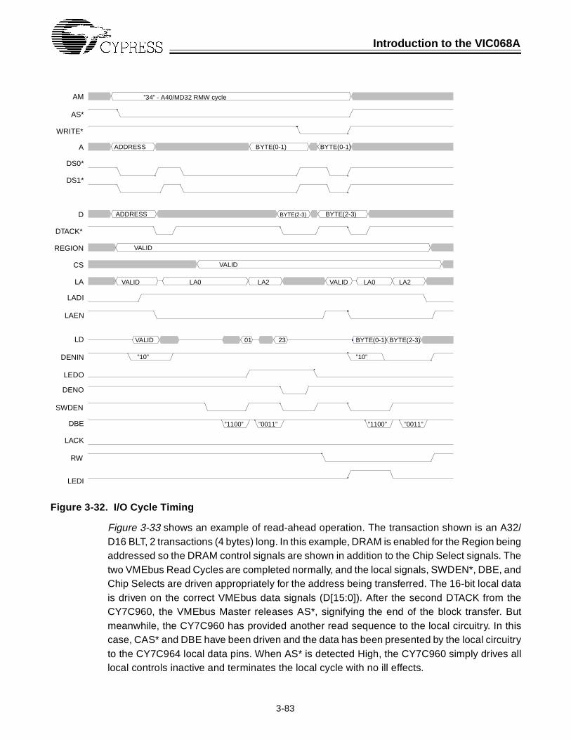
Introduction to the VIC068A
3-83
Figure 3-32. I/O Cycle Timing
Figure 3-33 shows an example of read-ahead operation. The transaction shown is an A32/D16 BLT, 2 transactions (4 bytes) long. In this example, DRAM is enabled for the Region beingaddressed so the DRAM control signals are shown in addition to the Chip Select signals. Thetwo VMEbus Read Cycles are completed normally, and the local signals, SWDEN*, DBE, andChip Selects are driven appropriately for the address being transferred. The 16-bit local datais driven on the correct VMEbus data signals (D[15:0]). After the second DTACK from theCY7C960, the VMEbus Master releases AS*, signifying the end of the block transfer. Butmeanwhile, the CY7C960 has provided another read sequence to the local circuitry. In thiscase, CAS* and DBE have been driven and the data has been presented by the local circuitryto the CY7C964 local data pins. When AS* is detected High, the CY7C960 simply drives alllocal controls inactive and terminates the local cycle with no ill effects.
”34” - A40/MD32 RMW cycle
ADDRESS
ADDRESS
BYTE(0-1)
BYTE(2-3)
BYTE(0-1)
BYTE(2-3)
VALID
VALID
”10” ”10”
”1100” ”0011” ”1100” ”0011”
LA0 LA2 VALID LA0 LA2
VALID
VALID
01 23 BYTE(0-1) BYTE(2-3)
AM
AS*
WRITE*
A
DS0*
DS1*
D
DTACK*
REGION
CS
LA
LADI
LAEN
LD
DENIN
LEDO
DENO
SWDEN
DBE
LACK
RW
LEDI

Introduction to the VIC068A
3-84
Figure 3-33. Example of Read-Ahead Timing
3.9.4 Data Byte Enable Usage
Table 3-10 indicates which Data Byte Enable signals are active for all possible VMEbusTransactions. The polarity assumed for the DBE pins is LOW true.
”0f” - A32/D16 SUPERVISORY BLT
VALID
BYTE(0-1)
”1100” ”001
01 23
VALID LA0 LA2 LA4
”1100”
01
VALID
VALID
BYTE(2-3)
AM
AS*
WRITE*
A
D
DS0*
DS1*
DTACK*
REGION
CS
LA
ROW
COL
RAS
CAS
LACK
LADI
LAEN
LD
SWDEN
LEDI
DENIN
LEDO
DENO
DBE
LDS
RW

Introduction to the VIC068A
3-85
Table 3-10. DBE Signal Truth Table
3.9.5 Using I/O In DRAM Mode
When the CY7C960 is configured for DRAM, three pins remain for use as Chip Select Outputs,CS[2:0]. When a transaction takes place that maps to a Region where DRAM is enabled theChip Select output pattern for that Region is driven from CS[2:0]. The DBE pins are drivenwith timing appropriate for a DRAM access (CAS* timing parameters configured during ini-tialization). When a transaction takes place that maps to a Region where DRAM is disabled,then the Chip Select pattern for that Region is driven from CS[2:0], and the DBE pins aredriven with timing appropriate for an I/O access (DBE assert time configured during initializa-tion).
DS1* DS0* LA1LA0
(LWORD*) DBE3 DBE2 DBE1 DBE0
Byte 0 1 0 1 1 1 1 0
1 0 0 1 1 1 0 1
0 1 1 1 1 0 1 1
1 0 1 1 0 1 1 1
Word 0 0 0 1 1 1 0 0
0 0 1 1 0 0 1 1
Longword 0 0 0 0 0 0 0 0
Unaligned 0 1 0 0 1 0 0 0
1 0 0 0 0 0 0 1
0 0 1 0 1 0 0 1
3-86
3.10 Design Considerations
3.10.1 Design Philosophy
The CY7C960 and the CY7C961 each share the basic VMEbus slave circuitry, and each hasa common design philosophy. The most basic foundation for the design was that of achievinghigh performance in whatever system the devices were placed. For the CY7C960, that phi-losophy determined the hierarchical partitioning of the design into several independent blocks,each with its own state machine. The coexistence of these state machines demanded a fully-synchronous internal design in order to remove the necessity for block-to-block synchroniza-tion circuitry, or pipelining. Thus the internal operations are all designed to take place withinone clock period, so that results from one state transition are available to other blocks in thecycle that they occur. No “analog” delays are employed in the design, and the standardVMEbus timings are determined by counting clock periods internally. The clock input frequen-cy that the two parts expect to see is 80 MHz: at this frequency all the VMEbus timings areassured. The design is fully static, and the clock frequency must therefore be consideredwhen specifying the configuration of the application. All parameters that are a function ofclock period are specified as such (e.g., 3T + 4 nsec) in the AC timing tables (Chapter 3.12).
There is a comprehensive set of timing diagrams in Chapter that should be consulted todetermine the relationship of the various signals. Where possible, there are AC timing pa-rameters specified in Table 3-16. In general, however, the diagrams will give a better under-standing of the operation of the parts than a table of numbers.
3.10.2 CY7C964 Interface
The operation of the interface is described in Chapter 3.6, and in Section 4, The CY7C964Bus Interface Logic Circuit. The background to this section may be of interest.
The first controller produced by Cypress for the VMEbus community was the ubiquitousVIC068A—the current industry-standard controller. This device was intended to be used inconcert with the state of the art in low-cost drivers—then “ACT” logic devices such as ‘543sand ‘245s. The control outputs from the VIC068A were crafted to interface cleanly with thesedevices. Thus LEDI, LEDO, DENIN*, DENO*, etc. from the VIC068A were signals whosetiming was designed to turn the drivers on or off, and latch the data and address buses, atappropriate times for the VMEbus transfers. When the VIC64 was introduced it inherited theidentical timings, because the VIC64 was socket-compatible with the VIC068A. The CY7C964was designed as a glueless companion to VIC64, replacing the ACT logic with a higher level
Design Considerations
3-87
of integration to allow the increased functionality of the VME64 specification to be implementedin similar board space. So it also inherited the control signal timing of the VIC068A.
Several of the control signals perform double duty, such as LDS and MWB*, which are usedduring the comparator load sequence in the CY7C964. But in general, the signals controllingthe ‘964 are the original buffer control signals from the VIC068A.
Therefore, when the CY7C960 and ‘961 were designed, they had to conform to the originalcontrol timing imposed by the VIC068A in order to use the popular CY7C964. Therefore thecontrol signals have the same names, functions, and timings as the original VIC068A and theVIC64. One advantage of this is that applications that do not require the sophistication of theVME64 specification are not forced into employing the sophisticated CY7C964—the controlsignals work with the FCT family of devices that are also offered by Cypress. These devicesallow simpler applications to achieve cost goals without sacrificing performance. The limita-tion, as should be expected, is that the more complex VMEbus transactions are not imple-mented unless the CY7C964 is employed.
3.10.3 Local Bus Philosophy
The CY7C960 and ‘961 are very flexible in the way they deal with local circuitry. However,they are not intended to compete with their more sophisticated cousins, VIC64 and VIC068A.Whereas VIC068A and VIC64 have a local bus arbitration circuit, on-chip DMA engine, andlocal interrupt circuitry, the ‘960 and ‘961 are conceptually much simpler. On the surface, thepinout reveals a simple local acknowledge handshake, and a local interrupt input. The ‘961also provides a local bus error function. Beneath the surface, there is another level of com-plexity that can be invoked by applications that need somewhat more local bus control.
The CY7C960 was intended to be the highest priority on the local bus. In other words, the‘960 assumes that when a VMEbus slave transaction occurs, nothing will prevent it fromreading or writing local transactions other than the local acknowledge handshake. The localcycle starts with no regard for other masters which may be accessing local resources. Thisoptimizes VMEbus performance, preventing VMEbus cycles being extended by local buscontention. However, this philosophy is not beneficial in all cases. Some rudimentary controlover the local bus may be needed from time to time by other devices.
To cater to this situation the CY7C960 can be prevented from starting a local cycle, or a refreshof local DRAM. To explain this operation, first consider the VMEbus activity. Whenever AS*is asserted by a VMEbus master, the CY7C960 will drive RAS* Low, and the VMEbus addressis driven onto the local address bus by the CY7C964s. This happens whether the CY7C960is addressed or not, in order to optimize performance. The problem for local bus ownershipis that there is no way to predict when AS* will go active. Hence the only way to guaranteethat AS* is not about to go Low, is to watch it go High. Then the AS* minimum High timeprovides a window of opportunity for the local master to capture the local bus from theCY7C960. The local signal which can be used to monitor AS* going High is LADI. This signalalso indicates DRAM refresh activity, thus preventing a conflict between the local bus master

Design Considerations
3-88
and a local DRAM refresh cycle. The local acknowledge signal is used to capture the localbus: if enabled to do so by a bit in the configuration sequence, the LACK pin prevents thestart of a ‘960 local cycle. If LACK is driven High (or is High already) when the windowdescribed earlier occurs, then no local signals are driven by the ‘960 whatever happens onthe VMEbus. Control signals to the ‘964 are driven to cause the least significant ‘964 to bethree-stated and the local bus master can now perform local cycles without fear of interventionor DRAM refresh. LAEN of the remaining ‘964s must be controlled by external logic. The localbus is given back to the CY7C960 upon the assertion of LACK (Low).
In some applications, VMEbus traffic may not provide enough opportunities—AS* may notcycle frequently. In such a case, the local master can still acquire the local bus by drivingLACK High, waiting a period of time (2T) then examining LADI. If LADI is still inactive thenthe local bus is available. If LADI is active, then the VMEbus transaction has begun and the‘960 is about to start a local bus access.
Note that, while the local bus is not available to the CY7C960, any VMEbus accesses to theCY7C960 will hang until the local bus is again available. Also, the refresh engine will be unableto refresh the DRAM; when LACK is driven Low, the refresh engine has priority and will burstall the missed refresh cycles (256 bursts) before the CY7C960 will respond to a VMEbus cycle.
Note that this function is enabled by a bit in the configuration bit stream. If the bit is not enabled,then the CY7C960 cannot be prevented from DRAM refresh, or from starting a local cycle.The function of LACK is then simply to control the completion of local cycles allowing for slowor asynchronous local peripherals.
3.10.4 Read-Ahead Cycles
The CY7C960 does not read ahead single-cycle transfers, but it does perform read-aheadcycles when acting as a slave to a VMEbus BLT read operation. There are two ways to preventCY7C960 performing the read-ahead, both involving the VMEbus Master: terminate the blocktransfer at a 256-byte address boundary; or remove AS* with the final DS* deassertion.
Read-ahead is implemented to allow a higher performance to be achieved, as otherwise theslave board will be unable to provide data within the specified timing for minimum transactionperiod.
There are considerations when designing FIFO-based slave circuitry in order to guaranteethat the master will be given an error-free block transfer. The FIFO going empty during theprogress of a block transfer Read will not be a problem, assuming that the circuitry externalto CY7C960 intercepts the read strobe until the FIFO has data, and does not acknowledgethe local cycle until the data has in fact been transferred to the CY7C960. The problem occurswhen a data block is desired that is not aligned to 256-byte address boundaries. The finaltransfer of desired data will be followed by a read-ahead cycle which will, unless interceptedin some way, clock exactly one more data location from the FIFO.

Design Considerations
3-89
In most applications this will not be a problem, as the system design is usually organized sothat the FIFO goes empty after the final desired data byte has been read, and the followingread-ahead will not be relevant. Once AS* has gone inactive on the VMEbus, the CY7C960understands that the data transfer is complete. It drives all local signals inactive, whether ornot the cycle has been locally acknowledged. This effectively discards the read-ahead.
In some cases the FIFO may contain relevant data at all times, and a read-ahead cycle wouldresult in loss of data. These applications must either ensure that the data is aligned to 256byte address boundaries, or ensure that AS* and DS* go inactive together, thereby ensuringthat the final cycle is not followed by a read-ahead.
3.10.5 Write Posting
A similar consideration is inherent in the BLT Write operation. A common system configurationon VMEbus is that the slave “posts” the write data and acknowledges the VMEbus cycle priorto the local acknowledge. This optimizes performance: without BLT write posting, performanceis substantially degraded, approximating that of a well-designed single cycle transfer.
During a BLT Write transfer, if the local circuitry detects an error or is unable to complete thetransaction, then the local circuitry will not acknowledge the posted data. This causes theVMEbus to extend the current cycle (the one immediately AFTER the posted transaction) andthe system timer will timeout, causing a BERR* and allowing the Master to perform errorrecovery.
In the event that the final local cycle of a block does not terminate correctly, there is nomechanism for communicating this error to the Master. The cycle has already been DTACKed,and the bus ownership has been relinquished. This is a problem common to all VMEbus SlaveWrite Posting applications.
The CY7C960 posts all BLT write transactions. If the system designer has a problem withwrite posting due to the last-cycle issue, then single cycle transfers must be used. CY7C960does not post single cycle write data.
3.10.6 VMEbus Error Considerations
Because of pinout limitations the CY7C960 does not monitor or drive BERR*, the VMEbuserror handshake. In the case where the VMEbus cycle terminates with a BERR*, indicatingthat the local data was in fact needed but was not provided before the VMEbus timer expired,CY7C960 cannot see BERR*, but still sees AS* go inactive. The CY7C960 always terminatesthe local cycle in response to AS* going inactive. In this case it is the responsibility of theMaster to take action following the BERR*. The CY7C960 continues to operate normally.

3-90
3.11 CY7C961 Description
3.11.1 Introduction
The CY7C961 is a CY7C960 Slave VMEbus Interface Controller with the addition of a masterblock transfer capability. Full-featured Slave boards can be built, using the CY7C961, thatoffer a flexible Master block transfer facility for bursting data across the VMEbus. The CY7C961can receive its instructions from a VMEbus Master or by programming registers locally. TheCY7C961 interprets the instructions and then moves data accordingly as a VMEbus Master.This optimizes performance and bus utilization.
The CY7C961 is a true superset of the CY7C960. Signal pins have been added to controlCY7C964 DMA functions. Unidirectional VMEbus pins have been changed to bidirectional.A few additional signals have been provided to complete a master interface, such as a dataport and VMEbus requester signals. As a VMEbus Slave, the CY7C961 behaves in everyrespect like the CY7C960. It has more pins, a master block transfer facility, and (because ofthe addition of BBSY*) full lock cycle support.
From a system perspective, this CY7C961 master block transfer capability can be viewed asa DMA channel which resides on the slave card, and is controlled by a dual ported on-chipregister file. It is possible to program the DMA channel from the VMEbus or from the localside of the interface, or both. Once programmed, the CY7C961 acquires the VMEbus andtransfers data in one of 20 user-selected protocols.
Circuitry on the local side of the CY7C961 sees the same control signals as were describedfor the CY7C960. For example, the REGION inputs to the CY7C961 are driven by an externaladdress decoder. The address decoder sits on the local address bus, which is driven fromthe CY7C964s. The local memory or I/O involved in the data transfer is enabled through theCS outputs and the DRAM control signals from the CY7C961, so they must be configuredcorrectly for the REGION inputs being driven.
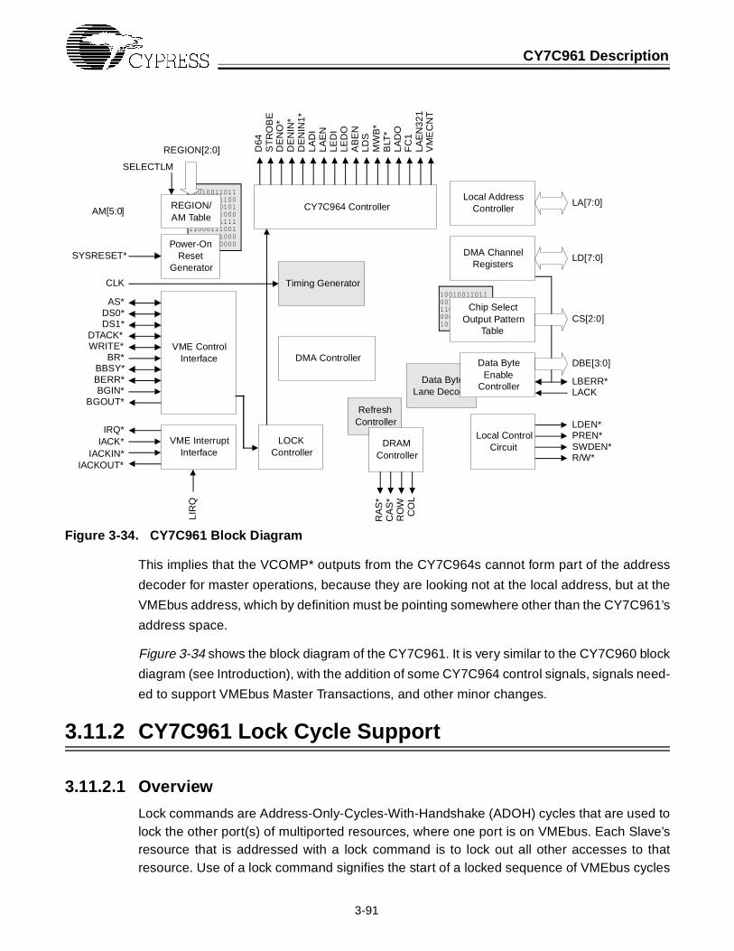
CY7C961 Description
3-91
Figure 3-34. CY7C961 Block Diagram
This implies that the VCOMP* outputs from the CY7C964s cannot form part of the address
decoder for master operations, because they are looking not at the local address, but at the
VMEbus address, which by definition must be pointing somewhere other than the CY7C961’s
address space.
Figure 3-34 shows the block diagram of the CY7C961. It is very similar to the CY7C960 block
diagram (see Introduction), with the addition of some CY7C964 control signals, signals need-
ed to support VMEbus Master Transactions, and other minor changes.
3.11.2 CY7C961 Lock Cycle Support
3.11.2.1 Overview
Lock commands are Address-Only-Cycles-With-Handshake (ADOH) cycles that are used tolock the other port(s) of multiported resources, where one port is on VMEbus. Each Slave’sresource that is addressed with a lock command is to lock out all other accesses to thatresource. Use of a lock command signifies the start of a locked sequence of VMEbus cycles
1001001101100101101100110001101010000000100010101011111
1001001101100101101100110001101010000000100010101011111110001110011011001100000000000000
RefreshController
Data ByteLane Decoder
VME ControlInterface
AS*DS0*DS1*
DTACK*WRITE*
BR*BBSY*BERR*BGIN*
BGOUT*
Timing Generator
DRAMController
RA
S*
CA
S*
RO
WC
OL
SYSRESET*Power-On
ResetGenerator
VME InterruptInterface
IRQ*IACK*
IACKIN*IACKOUT*
LIR
QREGION/AM Table
AM[5:0]
REGION[2:0]
Data ByteEnable
Controller
DBE[3:0]
Chip SelectOutput Pattern
TableCS[2:0]
Local ControlCircuit
PREN*
R/W*SWDEN*
LDEN*
CLK
SELECTLM
DMA Controller
Local AddressController
LA[7:0]
DMA ChannelRegisters
LD[7:0]
LOCKController
CY7C964 Controller
D64
ST
RO
BE
DE
NO
*D
EN
IN*
DE
NIN
1*LA
DI
LAE
NLE
DI
LED
OA
BE
NLD
SM
WB
*B
LT*
LAD
OF
C1
LAE
N32
1V
ME
CN
T
LACKLBERR*

CY7C961 Description
3-92
which ends with the end of the current VMEbus Master’s bus tenure. The CY7C961 allowslocked cycles to be decoded, and drives a local lock indicator while the ensuing VMEbuslocked sequence is in progress.
3.11.2.2 Description
Each of the lock commands (A16, A24, A32, A40, A64) consists of an address phase whichis presented to the VMEbus and handshaken by the targeted Slave. The CY7C961 can beprogrammed to decode lock commands on any ONE of its 16 decode regions. Any combina-tion of the five lock commands can be enabled for that region, but only one lock indicatorsignal is provided. When a lock command is decoded, the CY7C961 drives its MWB pin Lowto indicate the beginning of the locked VMEbus sequence. The lock indication on MWB willbe maintained as long as BBSY* or AS* remains asserted to the CY7C961. A decoded lockcycle will not cause chip selects or byte enables to become active. A decoded lock cycle willnot interfere in any way with slave accesses to the CY7C961. Figure 3-35 shows the timingof the various signals associated with LOCK cycles.
The MWB signal is active during block transfer register accesses and during CY7C961 masterblock transfers. MWB indicates a default lock condition during master block transfer. Thisshould be considered when designing the local resource lock control circuitry in which MWBis used. If the lock default is not needed during master block transfers, the CY7C961 signalFC1 can be used to disable lock during master block transfers.
3.11.3 CY7C961 Master Block Facility
3.11.3.1 Overview
The CY7C961 Master Block Facility provides “block transfer on demand” capability for slavecards built around the Cypress CY7C961/CY7C964 chip set. This facility allows DMA controlby writing a short series of commands to the CY7C961/CY7C964 chip set, telling it how muchdata to move, where to get it from, where to put it, and what transfer protocol to use whilemoving it. Blocks can be moved over the VMEbus as indivisible single cycles or BLTs. Theprotocol menu includes D8, D16, D32, MD32, or D64. A16, A24, A32, A40, and A64 addressspaces can be specified. Burst lengths from 16 bytes to 8 megabytes can be requested. Eightregisters accessible from the VMEbus or the local side of the interface make the facility simpleto configure and simple to control. The facility has a busy semaphore, a VMEbus Interrupt oncompletion feature with a programmable statusID byte, and a built in requester and bus grantdaisychain.

CY7C961 Description
3-93
Figure 3-35. LOCK Cycle Timing
It is expected that the system designer will choose either local programming of the DMAchannel or VMEbus programming and design decode and other support circuitry based onthat choice. There is nothing in the design of the CY7C961 to prevent dual porting of the DMAcontrol registers, but dual porting, like multi-master VMEbus control requires polling of theCY7C961 control register semaphore and/or added complexity in hardware and softwaredesign.
VMEbus locked sequence
DECODE delay
REFRESH BURST
Block transfer to DRAM
LCK
LOCK Indicator remains lentil AS* is deasserted after BBSY* has been deasserted.
A64/D16 BLT A24/Serial
VAL ADD VALID
VALID
VALID VALID
ADD
ADD
01 45 8923 67
LA0 LA4LA2 LA6 LA10 LA14 LA18LA8 LA12 LA16 LA20 LA22 LA24
01 45 8923 67 2425
”10” ”10”
VALID
etc.
etc.
BBSY*
MWB*
AM
AS*
WRITE*
A
D
DS0*
DS1*
DTACK*
LA
REGION
LADI
CS
LD
LEDI
DBE
SWDEN*
RAS*
CAS*
ROW
COL
LACK
DENIN*
R/W*
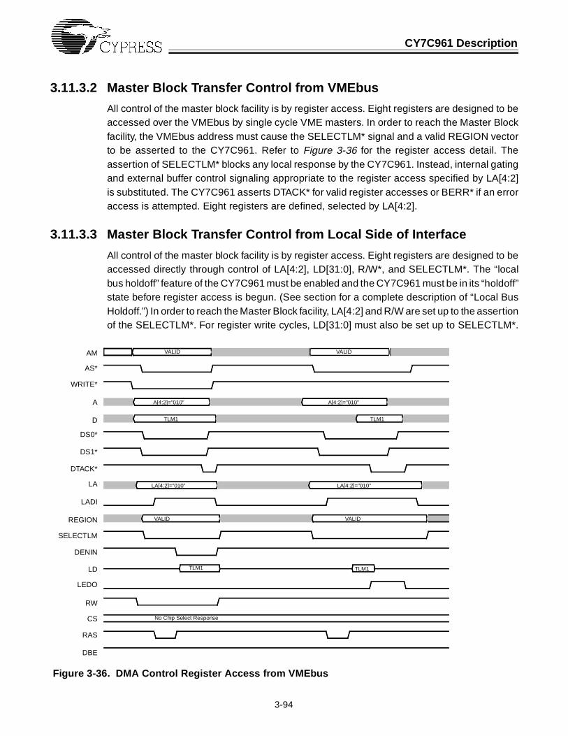
CY7C961 Description
3-94
3.11.3.2 Master Block Transfer Control from VMEbus
All control of the master block facility is by register access. Eight registers are designed to beaccessed over the VMEbus by single cycle VME masters. In order to reach the Master Blockfacility, the VMEbus address must cause the SELECTLM* signal and a valid REGION vectorto be asserted to the CY7C961. Refer to Figure 3-36 for the register access detail. Theassertion of SELECTLM* blocks any local response by the CY7C961. Instead, internal gatingand external buffer control signaling appropriate to the register access specified by LA[4:2]is substituted. The CY7C961 asserts DTACK* for valid register accesses or BERR* if an erroraccess is attempted. Eight registers are defined, selected by LA[4:2].
3.11.3.3 Master Block Transfer Control from Local Side of Interface
All control of the master block facility is by register access. Eight registers are designed to beaccessed directly through control of LA[4:2], LD[31:0], R/W*, and SELECTLM*. The “localbus holdoff” feature of the CY7C961 must be enabled and the CY7C961 must be in its “holdoff”state before register access is begun. (See section for a complete description of “Local BusHoldoff.”) In order to reach the Master Block facility, LA[4:2] and R/W are set up to the assertionof the SELECTLM*. For register write cycles, LD[31:0] must also be set up to SELECTLM*.
AM
AS*
WRITE*
A
D
DS0*
DS1*
DTACK*
LA
LADI
REGION
SELECTLM
DENIN
LD
LEDO
RW
CS
RAS
DBE
VALID VALID
A[4:2]=”010”
TLM1
A[4:2]=”010”
TLM1
LA[4:2]=”010” LA[4:2]=”010”
TLM1
VALIDVALID
TLM1
No Chip Select Response
Figure 3-36. DMA Control Register Access from VMEbus

CY7C961 Description
3-95
The response of the CY7C961 is self-timed and no acknowledge handshake is provided.SELECTLM* must be asserted for a minimum of 100 ns (eight CLK periods) and LA[4:2], R/W*, and LD[31:0] must be driven valid until SELECTLM* is deasserted. On register reads,CY7C961 drives LD[7:0] two clocks after SELECTLM* is sampled asserted and three-statesLD[7:0] one clock after SELECTLM* is sampled deasserted. Refer to Figure 3-37 for LocalRegister access signaling.
Figure 3-37. DMA Control Register Local Access
The CY7C961 provides control signals to the CY7C964 to control the loading of registersinside the device for operations such as establishing the local starting address and the VME-bus starting address, both of which could be 32-bit quantities stored inside the CY7C964s.
If an illegal register access is attempted, the CY7C961 will signal by driving LBERR* Lowwithin two clocks after SELECTLM* is asserted. LBERR* deasserts one clock after SE-LECTLM* is sampled deasserted.
3.11.3.4 Programming the Master Block Facility
In general, the set-up programming is very simple. First the semaphore must be read. Thisregister read unlocks the facility. Next, values are written to Transfer Length, Transfer Type,Upper Address (optional), and Master Block StatusID (optional). These parameters need notbe refreshed each time the facility is used. After that, the VME Starting Address is written,then Local Starting Address and GO. This last register write operation starts the block transfer.The CY7C961 will assert BR* and, upon being granted the VMEbus, move data until thetransfer length is exhausted.
Note that the CY7C961 can be programmed through the initialization bit stream to releaseand re-request the VMEbus at every 256-byte boundary as DMA transfer progresses. This
DATA from CY7C961
Register Address
VALID
DATA to CY7C961/CY7C964
CLK
LADI
LACK
RW
LAEN
LA[4:2]
LD(write)
SELECTLM
LD(read)
LBERR

CY7C961 Description
3-96
behavior can be useful in providing VMEbus access to high-priority traffic interleaved with theDMA transaction.
If more than one VMEbus master is to control the block transfer facility, or if the facility is dual-ported between a local and one or more VMEbus masters, the Semaphore Test & Set registercan be polled by any master to determine if the facility is “idle” or “busy.” If the polling resultis “idle”, that register read sets the semaphore to “busy”, eliminating the need for a read-modify operation. The semaphore can be written to “idle.” The semaphore is changed by theregister write, but this operation is always acknowledged with an error response by theCY7C961.
The semaphore is reset by the CY7C961 on block transfer completion. To do another blocktransfer requires a minimum of three register accesses, namely, (1) read Semaphore Test &Set, (2) write VME Starting Address, and (3) write Local Starting Address and GO. Of courseany of the set-up parameters can be read (with some limitations) or written before writing theGO register. Once the Local Starting Address and GO register is written, all register writeattempts are greeted with error acknowledge, cancellation of the DMA operation, and resetof the semaphore. Register reads are always permitted.
The CY7C961 is equipped with BERR* and LBERR* inputs which can be used to interrupt aDMA transfer at any time after it is started (BBSY* is asserted). No consideration as to thetiming of BERR* or LBERR* assertion with respect to the progress of the DMA needs to begiven. These signals provide a mechanism for aborting DMA transfers in favor of higher priorityVMEbus traffic.
Table 3-11. Master Block Transfer Control Registers
3.11.3.5 Register Definitions
The following descriptions apply equally to VMEbus register and local register access, butare written from the VMEbus perspective. Local access occurs in the context of “local busholdoff” as previously described, and has as its error response LBERR* substituted for BERR*.
LA[4:0] Register Function
000xx Semaphore Test & Set (read only)
001xx Transfer Length Multiplier 0 (TLM0)
010xx Transfer Length Multiplier 1 (TLM1)
011xx Transfer Type
100xx Local Starting Address and GO
101xx VME Starting Address
110xx A40/A64 Upper Address
111xx Master Block StatusID & Interrupt Enable

CY7C961 Description
3-97
3.11.3.5.1 Semaphore Test & Set (read only)
Location 000xx is a semaphore test and set. It is a read cycle. CY7C961 responds with thecurrent value of the semaphore. If the Master Block resource of the CY7C961 is idle, this readwill return logic “1” on LD0 which is reflected on D0 of the VME data bus. This register readcauses the semaphore to be set to busy. The CY7C961 will now respond to additional registeraccesses. Any subsequent read of the semaphore will return logic “0” on LD[0] and D[0]indicating that the block transfer resource is “busy.”
The semaphore is cleared by the CY7C961 upon completion of a block transfer or when anillegal combination of register values is held when a transfer is attempted. If the interrupt oncompletion feature is enabled, semaphore clear is delayed until the interrupt generated byblock transfer completion is serviced. When BERR* is received during a block transfer, thetransfer terminates and the semaphore is cleared. If the interrupt on completion feature isenabled, an interrupt will be signaled on termination and the semaphore clear is delayed untilthat interrupt is serviced.
Any write to location 000xx will cause the CY7C961 to drive BERR* and clear the semaphore.If access to any of the seven other defined registers is attempted before the semaphore is inthe “busy” state, CY7C961 will BERR* those attempts and the semaphore will remain in theidle state.
The CY7C961 drives status conditions on LD[6:1] passed through to D[6:1] of the VMEbusduring semaphore read. The normal value for these status bits is logic “1.” A logic “0” on anybit indicates a condition which would prevent a block transfer from starting (cause CY7C961to BERR a write to Local Starting Address and GO). Table 3-12 summarizes the semaphoreTest and Set Status Bit functions.
Table 3-12. Semaphore Test and Set Status Bits
A logic “0” on bit 1 means that interrupt on completion is enabled and a block transfer hasterminated or completed, but the interrupt signalled on termination/completion has not yetbeen serviced by a VMEbus interrupt handler. Bit 0 is always logic “0” in this case since the
Status Bit Error Indication
bit 0 Semaphore. (Logic “1” if idle)
bit 1 Master Block interrupt is pending.
bit 2 Transfer Length Multiplier registers are 0.
bit 3 Transfer Type is undefined.
bit 4 Data size is incompatible with VME or local starting address.
bit 5 Address alignment violated on multiplexed data BLT.
bit 6 VME starting address has not been updated.
bit 7 BERR* or LBERR* asserted during transaction.
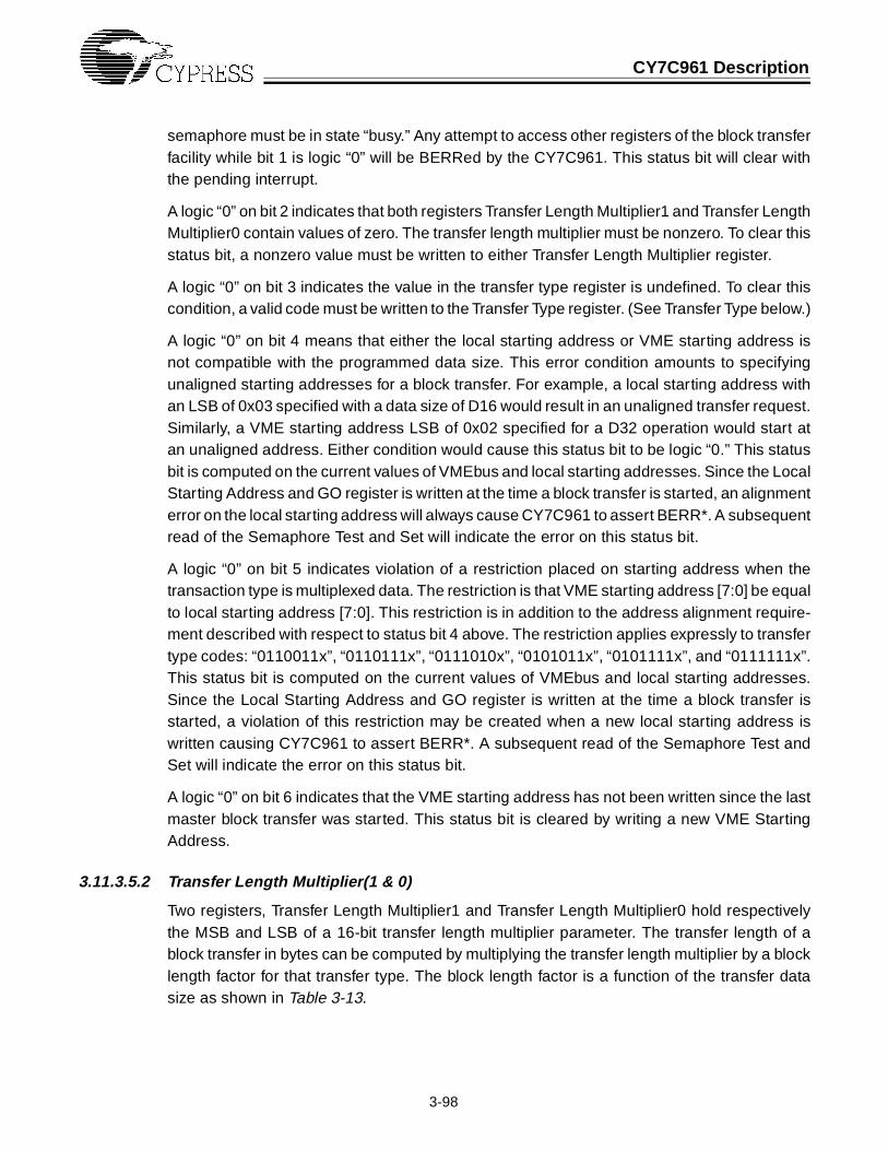
CY7C961 Description
3-98
semaphore must be in state “busy.” Any attempt to access other registers of the block transferfacility while bit 1 is logic “0” will be BERRed by the CY7C961. This status bit will clear withthe pending interrupt.
A logic “0” on bit 2 indicates that both registers Transfer Length Multiplier1 and Transfer LengthMultiplier0 contain values of zero. The transfer length multiplier must be nonzero. To clear thisstatus bit, a nonzero value must be written to either Transfer Length Multiplier register.
A logic “0” on bit 3 indicates the value in the transfer type register is undefined. To clear thiscondition, a valid code must be written to the Transfer Type register. (See Transfer Type below.)
A logic “0” on bit 4 means that either the local starting address or VME starting address isnot compatible with the programmed data size. This error condition amounts to specifyingunaligned starting addresses for a block transfer. For example, a local starting address withan LSB of 0x03 specified with a data size of D16 would result in an unaligned transfer request.Similarly, a VME starting address LSB of 0x02 specified for a D32 operation would start atan unaligned address. Either condition would cause this status bit to be logic “0.” This statusbit is computed on the current values of VMEbus and local starting addresses. Since the LocalStarting Address and GO register is written at the time a block transfer is started, an alignmenterror on the local starting address will always cause CY7C961 to assert BERR*. A subsequentread of the Semaphore Test and Set will indicate the error on this status bit.
A logic “0” on bit 5 indicates violation of a restriction placed on starting address when thetransaction type is multiplexed data. The restriction is that VME starting address [7:0] be equalto local starting address [7:0]. This restriction is in addition to the address alignment require-ment described with respect to status bit 4 above. The restriction applies expressly to transfertype codes: “0110011x”, “0110111x”, “0111010x”, “0101011x”, “0101111x”, and “0111111x”.This status bit is computed on the current values of VMEbus and local starting addresses.Since the Local Starting Address and GO register is written at the time a block transfer isstarted, a violation of this restriction may be created when a new local starting address iswritten causing CY7C961 to assert BERR*. A subsequent read of the Semaphore Test andSet will indicate the error on this status bit.
A logic “0” on bit 6 indicates that the VME starting address has not been written since the lastmaster block transfer was started. This status bit is cleared by writing a new VME StartingAddress.
3.11.3.5.2 Transfer Length Multiplier(1 & 0)
Two registers, Transfer Length Multiplier1 and Transfer Length Multiplier0 hold respectivelythe MSB and LSB of a 16-bit transfer length multiplier parameter. The transfer length of ablock transfer in bytes can be computed by multiplying the transfer length multiplier by a blocklength factor for that transfer type. The block length factor is a function of the transfer datasize as shown in Table 3-13.

CY7C961 Description
3-99
Table 3-13. Transfer Length Calculation
For example, if TLM1= 4 and TLM0 = 6 and the data size is D32 (specified in the TransferType register), then the transfer length for the block transfer would be 64 X 1030 = 65,920bytes. The number of data cycles is always 16 times the transfer length multiplier, so the databytes transferred is obviously proportional to the width of the transaction. The transfer lengthmultiplier registers are read/write with data sent/received on LD[7:0] and reflected on D[7:0]of the VMEbus. Bit 2 of the Semaphore Test and Set status word will be logic “0” if bothTLM1and TLM0 are set to 0. This is an error condition which will block a transfer start. Bothregisters are cleared to 0 after power up or SYSRESET*.
3.11.3.5.3 Transfer Type
The Transfer type register specifies which of 22 possible block transfer operations is to beperformed. The user can select from among A40BLT, D64MBLT, D32BLT, D16BLT, D8BLT,and single cycle block move options. The 8-bit hex codes shown in Table 3-14 are validcontents of the transfer type register:
Data Size Block Length Factor TLM1,TLM0 Transfer Length
D8 16 Bytes X TLM[15:0] = BYTES
D16 32 Bytes X TLM[15:0] = BYTES
D32 64 Bytes X TLM[15:0] = BYTES
D64 128 Bytes X TLM[15:0] = BYTES
Table 3-14. Transfer Type Field—Block Transfer Operations
Transfer Type[7:0] AmCode Block Transfer Desc ription
20,21,22,23,24,25 3F A24 supervisory block transfer (D8BLT or D16BLT or D32BLT)
A8,A9,AA,AB,AC,AD 3E A24 supervisory program access (D8 or D16 or D32)
B0,B1,B2,B3,B4,B5 3D A24 supervisory data access (D8 or D16 or D32)
66,67 3C A24 supervisory 64-bit block transfer (MBLT)
28,29,2A,2B,2C,2D 3B A24 nonprivileged block transfer (D8BLT or D16BLT or D32BLT)
B8,B9,BA,BB,BC,BD 3A A24 nonprivileged program access (D8 or D16 or D32)
A0,A1,A2,A3,A4,A5 39 A24 nonprivileged data access (D8 or D16 or D32)
6E,6F 38 A24 nonprivileged 64-bit block transfer (MBLT)
40,41,42,43 37 A40 block transfer (D8BLT or D16BLT)
74,75 37 A40 32-bit block transfer (MD32)
90,91,92,93,94,95 2D A16 supervisory access (D8 or D16 or D32)
98,99,9A,9B,9C,9D 29 A16 nonprivileged access (D8 or D16 or D32)

CY7C961 Description
3-100
Bits [2:1] of the Transfer Type register specify the data size of the block transfer. Table 3-15defines this Transfer Type field. The CY7C961 checks for consistency between transfer typeand data size. Illogical combinations will be reported on Semaphore Test and Set status bit3 as an undefined transfer type and will prevent the start of a block transfer.
Table 3-15. Transfer Type Field—Data Size
Bit 0 of the Transfer Type register specifies block transfer data direction. Logic “1” specifiesmaster read with data moving to the CY7C961 interface, logic “0” specifies master write withdata moving from the CY7C961interface to a VMEbus slave.
The transfer type register is read or written with data transmitted on LD[7:0] and reflected onD[7:0] of the VMEbus. Illegal codes cause block transfer to abort when the GO transaction isreceived. Both undefined transfer type fields and illogical transfer type data size combinationswill BERR when Local Starting Address and GO is written.
3.11.3.5.4 Local Starting Address & GO
The Local starting address and GO register is used to write the local block address to beused in the DMA block transfer. This address can be up to 32 bits of address informationprovided as VME data when the register is written. Local starting address is loaded directly
10,11,12,13,14,15 0F A32 supervisory block transfer (D8BLT or D16BLT or D32BLT)
C0,C1,C2,C3,C4,C5 0E A32 supervisory program access (D8 or D16 or D32)
C8,C9,CA,CB,CC,CD 0D A32 supervisory data access (D8 or D16 or D32)
56,57 0C A32 supervisory 64-bit block transfer (MBLT)
18,19,1A,1B,1C,1D 0B A32 nonprivileged block transfer (D8BLT or D16BLT or D32BLT)
D0,D1,D2,D3,D4,D5 0A A32 nonprivileged program access (D8 or D16 or D32)
D8,D9,DA,DB,DC,DD 09 A32 nonprivileged data access (D8 or D16 or D32)
5E,5F 08 A32 nonprivileged 64-bit block transfer (MBLT)
48,49,4A,4B,4C,4D 03 A64 block transfer (D8BLT or D16BLT or D32BLT)
7E,7F 00 A64 64-bit block transfer (MBLT)
Transfer Type [2:1] Block Transfer Data Size
00 D8
01 D16
10 D32
11 D64
Table 3-14. Transfer Type Field—Block Transfer Operations (continued)
Transfer Type[7:0] AmCode Block Transfer Desc ription
CY7C961 Description
3-101
into the CY7C964’s local address counters C1 and the CY7C961 local address register. Aread of the local starting address will yield only the LSB of the starting address on LD[7:0]reflected on D[7:0] of the VME data bus.
The CY7C961 signal BLT* is driven low for 2 CLK periods to load the local address into theCY7C964s from the LD bus. The value of LD on the rising edge of BLT* is stored in theCY7C964 counter C1. Refer to Figure 3-38.
The control function of this register is activated only for writes to the register. GO causes thestart of the block transfer by signaling the CY7C961 requester to take the VMEbus and beginthe transfer. Once CY7C961 acquires the VMEbus, it will not release the VMEbus until theblock transfer finishes or is terminated by a BERR* during a transfer attempt. BBSY* is re-leased when the transfer length count is exhausted, not at VMEbus boundary crossings. Any
AM
AS*
WRITE*
A
D
DS0*
DS1*
DTACK*
LAEN321
BLT*
MWB*
LA
LADI
REGION
SELECTLM*
LD
DENIN*
LEDO
R/W*
CS
RAS*
DBE
BR*
BBSY*
VALID VALID
VALID VALID
LOCAL START ADDR BYTE0 BYTE1 BYTE2 BYTE3 BYTE4
Local Start Address latched on rising edge of BLT
VALID VALID LA0 LA1 LA2 LA3 LA4
VALID VALID VALID
VALID B0 B1 B2 B3 B4
VALID
0 1 2 3 0
Figure 3-38. Local Starting Address and Go, Block Tran sfer Start Timing

CY7C961 Description
3-102
write to a set-up register after the GO transaction will be BERRed by CY7C961, the blockmove aborted, and the semaphore reset.
3.11.3.5.5 VME Starting Address
The VME Starting Address register is used to write the VMEbus block address to be used inthe DMA block transfer. This address can be up to 32 bits of address information written asVME data to the CY7C961. It is actually stored in latch L9 of the CY7C964s and the LSB ofthe address is also captured by the CY7C961 to facilitate counting to the VME addressboundary. A read of the VMEbus Starting Address will yield only the LSB of the startingaddress on LD[7:0] reflected on D[7:0] of the VME data bus. Note that this specifier is a truebyte address. The CY7C961 takes care of VMEbus LWORD* and DS1*/DS0* encoding. Thisregister must be written each time a block transfer is executed. Bit 6 of the Semaphore Testand Set status register will indicate when the VME starting address has not been updated.This requirement guarantees that the CY7C964 and CY7C961 will be using the same VMEbusstarting address.
3.11.3.5.6 A40/A64 Upper Address
A40/A64 Upper Address register is not a register residing in either the CY7C961 or CY7C964.Instead, it is a facility for reading/writing extended address information to external hardwareon the slave card that is not part of the CY7C961/CY7C964 interface. Latch and enablesignaling allows for reading and writing during register access as well as data enable duringaddress broadcast as the DMA block transfer runs. A40 and A64 extensions are supported.
The latch signal for capturing extended address from the local data bus is (SELECTLM* &LEDI) where LEDI is a CY7C961 output. The active Low enable for driving the latched dataonto the local data bus is (LDEN* | MWB*). If the extended address is to be incremented,VCOUT* of the appropriate CY7C964 and LADO are used as count enable and clock respec-tively for extended address counting. Refer to Figure 3-39 for signaling.
The latch signal is designed to latch up to 32 bits of upper address from LD[31:0] passedthrough the interface from VME D[31:0] when Upper Address is written. The enable signal isdesigned to allow the stored address to be read from the VMEbus when Upper Data is read,as well as to enable the stored address onto LD when the master block transfer addressbroadcast requires it.
3.11.3.5.7 Master Block StatusID & Interrupt Enable
Master Block status ID & Interrupt Enable is a CY7C961 register which holds the Master BlockstatusID byte. This register can be read or written. Bits 7–1 of the register will be reflected inthe statusID byte sourced by CY7C961 when the Master Block interrupt is serviced. Bit 0controls enabling of interrupt on completion: logic “1” enables interrupt on completion.

CY7C961 Description
3-103
When the interrupter status is read by the handler, bit 0 of the statusID indicates completionstatus. Logic “1” means normal completion. Logic “0” means abnormal termination (BERR*or LBERR* was received during block transfer). The interrupter is a Release on Acknowledge(ROAK) interrupter. If interrupt on completion is enabled, CY7C961 will reset its semaphoreon interrupt acknowledge. If interrupt on completion is not enabled, CY7C961 will reset itssemaphore with BBSY deassertion at the end of the DMA block transfer. Refer to Figure 3-40 for Interrupter timing.
AM
AS*
WRITE*
A
D
DS0*
DS1*
DTACK*
LA
LADI
REGION
SELECTLM*
LD
LDEN*
MWB*
LEDI
DENIN*
LEDO
R/W*
CS
RAS*
DBE
VALID VALID
A[4:2] = “110” A[4:2] = “110”
UPPER ADDR UPPER ADDR
LA[4:2] = “110” LA[4:2] = “110”
VALID VALID
UPPER ADDR U.A.
Enable Upper Address!(MWB+LDEN)
Latch Upper Address 25 ns(!SELECTLM * LEDI)
No Chip Select Response
Figure 3-39. Upper Address Register Access Timing

CY7C961 Description
3-104
AM
AS*
IRQ*
IACK*
IACKIN*
WRITE*
VMECNT
A
D
DS0*
DS1*
DTACK*
MWB*
LA
LADI
REGION
CS
LD
LEDI
DENIN*
LEDO
LACK
DBE
RAS*
R/W*
BBSY*
“0a” - A32/D32 supervisory program access
A_last-8 A_last-4 A_last IRQ_level
St. Id
LA_last-8 LA_last-4 LA_last IRQ_level
Status/Id
Figure 3-40. Interru pter Timin g

CY7C961 Description
3-105
3.11.4 Pin Description Addendum
The following signals are either additional to, or redefined from, the CY7C960 pin descriptionsin Chapter 3.3.
3.11.4.1 VMEbus Signals
AM[5:0] - VMEbus Address Modifier
Input: YesOutput: YesDrive: 48 mA
Signals AM[5:0] are the VMEbus Address Modifier I/Os. When inputs, these signals are usedto decode the VMEbus data transaction type. The CY7C961 provides support for both pre-defined and user-defined VMEbus Address Modifiers. During master block transfers VMEbusAM codes are driven out on these signal pins.
AS* - VMEbus Address Strobe
Input: YesOutput: YesDrive: 64 mAActive: Low
LA7LA6LA5LD7LA4SELECTLM*LBERR*IRQ*N/CLA3LAEN321GndAM5LA2BBSY*VccLA1N/CDS1*N/CLWORD*FC1LDSDENIN1*LAEN
PR
EN
SW
DE
NR
AS
*/C
S4
LD3
CA
S*/
CS
5LD
4N
/CA
M2
N/C
RO
W/C
S2
LD5
CO
L/C
S3
AM
1G
ndB
R*
DB
E0
AM
0N
/CV
ccLD
6D
BE
1G
ndD
BE
2D
BE
3R
/W*
DE
NO
*IA
CK
OU
T*
IAC
KIN
*B
GO
UT
*IA
CK
*M
WB
*N
/C AS
*N
/CLA
DI
ST
RO
BE
BG
IN*
AB
EN
*D
TAC
K*
Gnd
N/C
DS
0*N
/C Vcc
BLT
*S
YS
RE
SE
T*
LAD
OD
64LE
DO
LED
I
LACKLIRQ*
LDEN*LD1CS0VccLD2CS1N/C
AM3REGION3/CS2
AM4Vcc
BERR*Gnd
VMECNTREGION2
LD0CLKN/C
WRITE*N/C
REGION1REGION0
DENIN*
CY7C961
TQFP
Top View
Pin 1

CY7C961 Description
3-106
Address Strobe is the VMEbus signal that informs VMEbus slaves that a valid address is onthe VMEbus. This signal is used by the CY7C961 to qualify the VMEbus Address ModifiersAM[5:0] and REGION[3:0] inputs to determine if a valid slave cycle should be performed.During master block transfers VMEbus AS* is driven out on this signal pin.
DS0*,DS1* - VMEbus Data Strobes
Input: YesOutput: YesDrive: 64 mAActive: Low
DS0* and DS1* are the VMEbus Data Strobes. As inputs, these signals inform the CY7C961that the data phase of the VMEbus cycle has begun. These signals in conjunction with theVMEbus LWORD* (connected to LA[0]) signal encode the data transfer width or number ofbytes, 1 through 4. This information is necessary to enable the appropriate CY7C964 databytes. During master block transfers VMEbus DS0* and DS1* are driven out on these signalpins.
WRITE* - VMEbus Write Line
Input: YesOutput: YesDrive: 48 mAActive: Low
The VMEbus WRITE* line specifies the data direction of the VMEbus data cycle in progress.If this signal is asserted then a VMEbus WRITE operation is in progress. During such atransaction, if the VMEbus address decodes properly, the CY7C961 responds by assertingthe local R/W* signal and performing the appropriate local cycle. During master block trans-fers, VMEbus WRITE* is driven out on this signal pin indicating the direction of data for theDMA transfer.
DTACK* - VMEbus Data Acknowledge
Input: YesOutput: YesDrive: 64 mAActive: Low
The DTACK* signal is asserted by the CY7C961 when a valid VMEbus transaction is inprogress and has remained valid for the proper length of time. The assertion of this signalinforms the VMEbus Master that the slave has either accepted the data during write operationsor has sourced the data during read operations. This signal is a rescinding output. Duringmaster block transfers, the CY7C961 receives VMEbus data acknowledge from the targetslave.

CY7C961 Description
3-107
BR* - VMEbus Request
Input: NoOutput: YesDrive: 48 mAActive: Low
Signal BR* is the VMEbus Request output. This output is open-collector with a low state sinkcurrent of 48 mA. It is asserted by the CY7C961 when the VMEbus is required for a blocktransfer.
BGIN* - VMEbus Bus Grant In
Input: YesOutput: NoActive: Low
BGIN* is a VMEbus Bus Grant In signal. It is generated by the VMEbus arbiter and signalsthat CY7C961 may use the VMEbus. BGIN* and BGOUT* signals form a bus grant daisy chain.
BGOUT* - VMEbus Bus Grant Out
Input: NoOutput: YesDrive: 8 mAActive: Low
BGOUT* is a VMEbus Bus Grant Out signal. It is driven Low by the CY7C961 in response toan assertion of the BGIN* signal when CY7C961 does not want to use the VMEbus.
BBSY* - VMEbus Bus Busy
Input: YesOutput: YesDrive: 64 mAActive: Low
BBSY* is the VMEbus bus busy signal. It is driven Low by the CY7C961 to indicate the VMEbusis being used for a block transfer. When the block transfer operation is done, CY7C961 drivesBBSY* High and then three-states the signal. In response to decoded VMEbus lock cycles,the CY7C961 monitors BBSY* to determine when a locked VMEbus sequence is ending.
BERR* - VMEbus Bus Error
Input: YesOutput: YesDrive: 48 mAActive: Low
BERR* is the VMEbus bus error signal. It is driven Low by CY7C961 in two cases. First,decoded slave accesses which attempt to illegally configure the CY7C961 block transferfacility will result in a BERR* acknowledge. Second, BERR* will be signaled to acknowledgea slave block data cycle if LBERR* is sampled asserted at the time VMEbus DSA* was received
CY7C961 Description
3-108
by the CY7C961. BERR* is three-stated on the deassertion of VMEbus signals DS0* andDS1*. CY7C961 monitors BERR* during master block transfer operation, truncating the blocktransfer if a BERR* acknowledge is detected. BERR* assertion will also signal the end of anylocked VMEbus sequence.
3.11.4.2 Local Buffer Control Signals
BLT*
Input: NoOutput: YesDrive: 8 mAActive: Low
BLT* is driven Low for 2 clock periods during the block transfer register access “Local startingaddress and GO.” The local starting address for block transfer is latched into CY7C964 internalcounters on the High-going edge of this signal. The CY7C961 BLT* pin should be connectedto the BLT* pin of each CY7C964 in the interface.
MWB*
Input: NoOutput: YesDrive: 8 mAActive: Low
MWB* is driven Low by CY7C961 during the block transfer register access “Local startingaddress and GO.” It remains in the Low state throughout master block transfer except at 256-byte local boundaries. When a 256-byte local boundary is crossed, MWB* will be pulsed Highfor one clock period. The High to Low transition on this pulse increments the interfaceCY7C964 local block counters. MWB* is deasserted on completion of a block transfer. MWB*also signals VMEbus lock status. MWB* is driven Low on decode of a VMEbus lock cycle. Itis deasserted when the VMEbus lock sequence is complete. The CY7C961 MWB* pin shouldbe connected to the MWB* pin of each CY7C964 in the interface.
LADO
Input: NoOutput: YesDrive: 8 mA
LADO is pulsed High by CY7C961 at VMEbus 256-byte boundaries during master blocktransfers. LADO is driven High at the same time VMEbus data strobes are asserted for thelast cycle of the address page. LADO is driven Low one clock after DTACK* is detected Lowin that cycle. The High to Low transition on LADO increments the VMEbus block counters ofthe interface CY7C964s. The CY7C961 LADO pin should be connected to the LADO pins ofall interface CY7C964s EXCEPT the one connected to VMEbus addresses A[7:1].

CY7C961 Description
3-109
FC1
Input: NoOutput: YesDrive: 8 mAActive: High
FC1 is driven High by CY7C961 at the beginning of the block transfer’s VMEbus tenure. It isdeasserted at the end of the block transfer’s VMEbus tenure. The CY7C961 FC1 pin shouldbe connected to the FC1 pins of each CY7C964 in the interface. This signal can serve as aDMA complete indicator for local control purposes.
VMECNT
Input: NoOutput: YesDrive: 8 mA
VMECNT is a clock signal driven by CY7C961 to the LADO pin of the CY7C964 connectedto VMEbus addresses A[7:1]. This signal adjusts the VMEbus block counter of this CY7C964to source LWORD correctly for D8 and D16 block transfers. VMECNT also burst clocks thisblock counter to $h00 in cases where the VMEbus block starting address is not aligned to a256-byte boundary. The clock pulse width is one CLK period.
LAEN321
Input: NoOutput: YesDrive: 8 mAActive: High
LAEN321 is driven Low for four CLK periods during the block transfer register access “Localstarting address and GO.” The High to Low transition happens one clock before the High toLow transition on BLT*. LAEN321 is used in conjunction with BLT* and MWB* to place theinterface CY7C964s in BLT_STATE. The CY7C961 LAEN321 pin should be connected to theLAEN pins of all interface CY7C964s EXCEPT the one connected to VMEbus addressesA[7:1].
3.11.4.3 Local Signals
LD[7:0] - Local Data Signals
Input: YesOutput: YesDrive: 8 mA
LD[7:0] make up the local bidirectional data bus. These pins should be connected to LD[7:0]of the interface CY7C964 connected to VMEbus data D[7:0]. During block transfer registeraccesses and block transfer complete interrupt acknowledge accesses, data is read from orwritten to the CY7C961 via this data port.

CY7C961 Description
3-110
SELECTLM* - Select Load Master Signal
Input: YesOutput: NoActive: Low
SELECTLM* is a chip select for accessing the eight CY7C961 registers that control the blocktransfer facility. A decoded VMEbus slave cycle for which SELECTLM* is also asserted willbe interpreted by CY7C961 as a block transfer register access. SELECTLM* timing shouldimitate that of the REGION input.
LBERR* - Local Bus Error Signal
Input: YesOutput: YesDrive: 8 mAActive: Low
LBERR* has three distinct functions. First, it provides a mechanism for aborting DMA transfersin progress. At any time after the GO register access completes, LBERR* may be assertedto cause DMA completion (with error status). If interrupt on completion is enabled, IRQ* willbe asserted within two CLK periods after LBERR* assertion. A second function of LBERR*is as an error signaling mechanism for slave block transfer. Each time the VMEbus DSA*signal is asserted to the CY7C961, the state of the LBERR* signal is sampled. If it is asserted,that VMEbus cycle will receive a BERR* acknowledge instead of a DTACK* acknowledge.The third function of LBERR* is as an error acknowledge output for DMA register accessesduring “local bus holdoff.” LBERR* will be asserted (driven low) by CY7C961 to indicate anerror condition during a register access in progress. Note that LBERR* is always driving outof the CY7C961 during “local bus holdoff.”
R/W* - Read/Write
Input: YesOutput: YesDrive: 8 mA
R/W* is the local signal that determines if the cycle in progress is a read operation or a writeoperation. The CY7C961 asserts this signal Low during write operations.
When accessing the Master Block Facility from the local side of the interface - R/W* is aninput to the CY7C961. The local bus holdoff feature of the CY7C961 must be enabled beforeregister access is initiated.
3.11.4.4 Master Block Transfer Performance
From the perspective of local bus timing, there is no difference between local bus signalingfor master DMA and slave accesses. The master block facility uses the same circuits and thesame self-timed acknowledge constants as the slave. Master block transfers sample REGION
CY7C961 Description
3-111
at each 256-byte boundary. This allows a block transfer to, for example, start in an SRAMregion and transparently cross a hardware boundary into a DRAM region.
The master block facility has performance limits set by CY7C961 internal synchronous statemachines. 6 CLK periods is the minimum required per VMEbus data cycle for master writeoperations, 7 CLK periods for master read VMEbus data cycles. Local bus signaling limitsD64 transfer rates to 80 megabytes per second, and MD32 to 40 megabytes/second. Theperformance of D32 block transfer is limited by VMEbus slave response, with an ideal slaveresponse making block read performance of 40 megabytes/second and block write perfor-mance of 50 megabytes per second possible. These are, of course, burst maximums. Sus-tained D64 block transfer rate will be 73 megabytes/second to an ideal slave with local cyclesset up for 50 ns.
The block transfers using single-cycle protocol will be considerably slower than the true block
protocols because the CY7C961 must increment the CY7C964 after each data cycle. For
D32 this represents an 8 CLK period overhead. Transfer rate will not exceed 20 megabytes/
second. D16 single-cycle protocol will be down around 12 megabytes/second. D8 single-cycle
will top out at 5.5 megabytes/second.
For BLT transfers, CY7C961 will cross VME address boundaries without releasing the VME-
bus unless the Interleave function is programmed ON in the serial bit stream. Address strobe
will be cycled and address rebroadcast. BBSY does not have an early release mode, and is
asserted throughout the block transfer. D64MBLT will rebroadcast at 256-byte boundaries. If
single-cycle accesses are specified, the block move will consist of an indivisible packet of
single-cycle transfers sufficient to satisfy the transfer length parameter, transfer type dictating
the AM code used.

CY7C961 Description
3-112
3.11.5 Examples of Block Transfers
Figure 3-41. A64/D64 MBLT Master Write
AM
AS*
WRITE*
A
D
DS0*
DS1*
DTACK*
REGION
CS
LA
MWB*
LDEN*
LD
LEDO
DENIN*
RAS*
DBE
LACK
R/W*
BBSY*
“00” - A64/D64 MBLT
ADDRESS ADDRESSDATA0 DATA8 DATA16 DATA24 DATA32
UPP. ADDR. UPP. ADDR.DATA4 DATA12 DATA20 DATA28 DATA36
VALID (DRAM REGION)
VALID VALID
LA0 LA4 LA8 LA12 LA16 LA20 LA24 LA28 LA32 LA36 LA40 LA44
UPPER ADD. UPPER ADD.

CY7C961 Description
3-113
Figure 3-42. CY7C961 A64/D64 MBLT Master Read Example
AM
AS*
WRITE*
A
D
DS0*
DS1*
DTACK*
REGION
CS
LA
MWB*
LDEN*
LD
LEDI
DENIN*
RAS*
DBE
LACK
R/W*
BBSY*
“00” - A64/D64 MBLT
BOUNDARY
ADDRESS
UPP. ADD.
ADDRESS
UPP. ADD.
VALID (DRAM REGION)
VALID VALID
LA0 LA4 LA8 LA12 LA16 LA20 LA24 LA28 LA32 LA36 LA
UPPER ADD. UPPER ADD.0 4 8 12 16 20 24 28 32 36 40
“01” “01” “01” “01” “01” “01” “01”
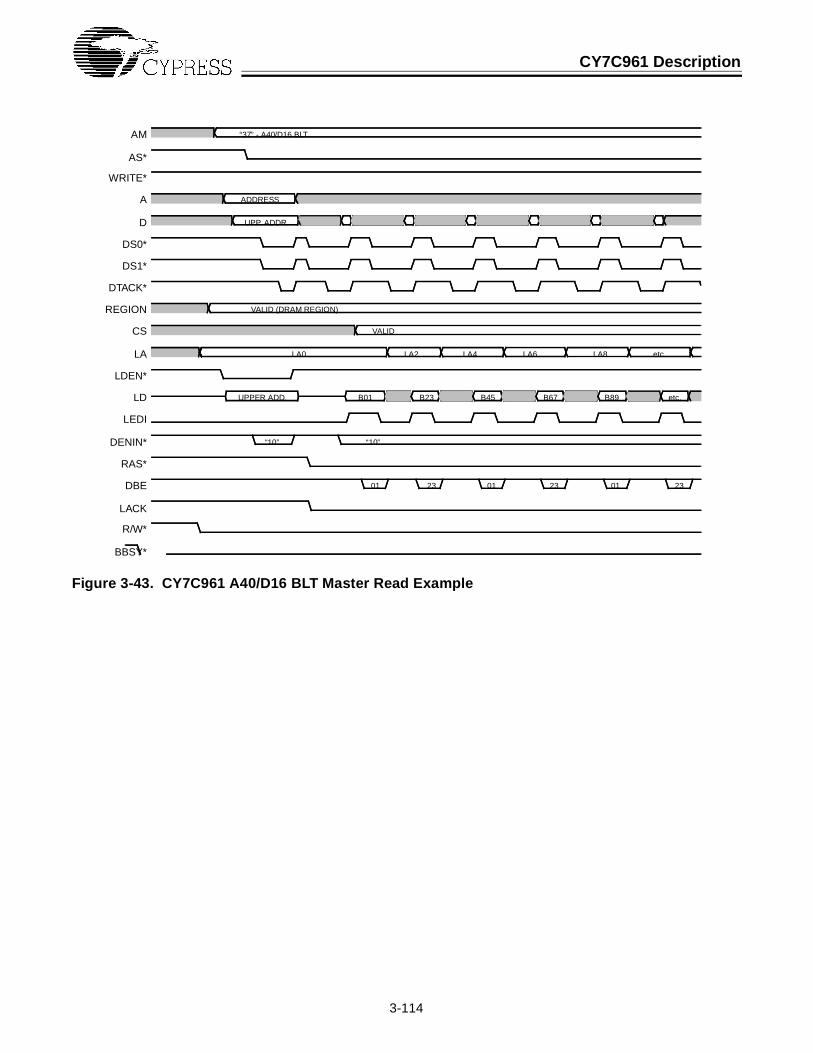
CY7C961 Description
3-114
Figure 3-43. CY7C961 A40/D16 BLT Master Read Example
AM
AS*
WRITE*
A
D
DS0*
DS1*
DTACK*
REGION
CS
LA
LDEN*
LD
LEDI
DENIN*
RAS*
DBE
LACK
R/W*
BBSY*
“37” - A40/D16 BLT
ADDRESS
UPP. ADDR.
VALID (DRAM REGION)
VALID
LA0 LA2 LA4 LA6 LA8 etc.
UPPER ADD. B01 B23 B45 B67 B89 etc.
“10” “10”
01 01 0123 23 23

CY7C961 Description
3-115
Figure 3-44. A32/D32 Single Cycle Write Example
AM
AS*
WRITE*
VMECNT
A
D
DS0*
DS1*
DTACK*
MWB*
LA
REGION
CS
LD
LEDO
LACK
DBE
RAS*
R/W*
BBSY*
“0e” - A32/D32 supervisory program access
Burst clock increments CY7C964
A0 A4 A8 A12 A16
D0 D4 D8 D12 D16
MWB increments LA
LA0 LA4 LA12LA8 LA16 LA20

3-116
3.12 AC Parameters
This addendum contains waveforms that describe the behavior of the CY7C960/961/CY7C964 interface for a variety of transaction types and timings. A table of AC parametersis referenced to the waveforms. Note that “T” refers to the CLK input period. Note also thatparameters are not indicated on the waveforms everywhere they apply. These waveformswere captured during in-system simulation and reflect accurately the behavior that can beexpected.
Clock Input
Note:
1. A 60/40 to 40/60 duty cycle must be maintained.
Num. Characteristic Min. Max.
Frequency of Operation (MHz) 30 80
1 Cycle Time (ns) 12.5 33.3
2, 3 Clock Pulse Width (Measured from 1.5V to 1.5V) Note 1 Note 1
4, 5 Rise and Fall Time (ns) — 5
Table 3-16. AC Parameters
Parameter Description Min Max Reference Notes
p1 DECODE Delay 2T 5T 2
p2 RAS*/CAS* Delay 2T 9T 2
p3 CAS* Width/DBE Width 3T 18T 2, 7
p4 CAS* Precharge 1T 8T 2
p5 RAS* Precharge 5T 12T 2
t2 LD to D 19 ns Waveform 5 3
t3 A to LA 20 ns Waveform 5 3
t4 D to LD 22 ns Waveform 20 3
0.8V
2.2V
4 5
1
32

AC Parameters
3-117
t5 LD to A Propagation Delay 22 ns Waveform 11 3
t7 ABEN* falling to A Output Enable Delay 12 ns Waveform 11 3
t8 DENO* falling to D Output Enable Delay 16 ns Waveform 5 3
t9 ABEN* falling to D Output Enable Delay 17 ns Waveform 11 3
t11 LAEN rising to LA 12 ns Waveform 18 3
t12 DENIN* falling to LD Output Enable Delay 18 ns Waveform 9 3
t13 DENIN1* falling to LD Output Enable Delay 21 ns Waveform 23 3
t15 ABEN* rising to A High-Z 12 ns Waveform 22 3
t16 DENO* rising to D High-Z 15 ns Waveform 3 3
t17 ABEN* rising to D High-Z 15 ns Waveform 22 3
t19 LAEN falling to LA High-Z 15 ns Waveform 18 3
t20 DENIN* rising to LD High-Z 18 ns Waveform 9 3
t23 A valid to VCOMP* falling 21 ns Waveform 3 3
t25 LD set-up to LEDO rising 7 ns Waveform 22 3
t26 LD hold to LEDO rising 0 ns Waveform 22 3
t28 LD set-up to DENO* falling 0 ns Waveform 22 3
t29 LD hold to DENO* falling 7 ns Waveform 22 3
t37 A, D set-up to LEDI rising 7 ns Waveform 23 3
t38 A, D hold after LEDI rising 0 ns Waveform 23 3
t45 LD set-up to STROBE rising 5 ns 3
t46 LD hold after STROBE rising 5 ns 3
t74 LDS rising to LD valid 24 ns Waveform 23 3
t75 LDS falling to LD valid 24 ns Waveform 23 3
t138 LADI falling to LA[31:8] valid 18 ns Waveform 18 3
s1 CLK period 12.5ns 33.3ns Waveform 4
s2 CLK pulse width 5 ns Waveform 4
s3 AS* falling edge to CS p1 + 1T p1 + 2T Waveform 1
s4 DSA* falling edge to CS 1T 2T Waveform 4
s5 AS* falling edge to REGION valid p1 – 1T Waveform 18
s6 AS* falling edge to RAS* falling 2T 3T Waveform 6
s7 ROW set-up to RAS* falling 1T Waveform 3
s8 PREN* falling to PCLK rising 80T Waveform 26
s9 COL set-up to CAS*, DBE falling 1T Waveform 3
s10 ROW deassertion to CAS* falling, DBE 1T Waveform 6
s11 LACK* rising set-up to prevent CAS* falling p2 – 1T Waveform 25 4
s12 LACK* falling to CAS* falling,DBE 2T 3T Waveform 25
s13 DSA* falling to CAS* falling,DBE 3T 4T Waveform 4
s14 SWDEN* set-up to CAS* falling,DBE 1T Waveform 12
Table 3-16. AC Parameters (continued)
Parameter Description Min Max Reference Notes
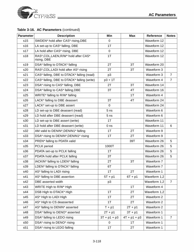
AC Parameters
3-118
s15 SWDEN* hold after CAS* rising,DBE 0 Waveform 12
s16 LA set-up to CAS* falling, DBE 1T Waveform 12
s17 LA hold after CAS* rising, DBE 0 Waveform 12
s18 RAS*,COL,LAEN,R/W* hold after CAS* rising, DBE
1T Waveform 12
s19 DSA* falling to DTACK* falling 2T 3T Waveform 20
s20 RAS*,COL,LADI hold after AS* rising 2T 3T Waveform 3
s21 CAS* falling, DBE to DTACK* falling (read) p3 Waveform 3 7
s22 CAS* falling, DBE to DTACK* falling (write) p3 + 1T Waveform 4 7
s23 DSA* rising to CAS* falling, DBE 2T 3T Waveform 14
s24 DSA* falling to CAS* falling,DBE 3T 4T Waveform 16
s25 WRITE* falling to R/W* falling 1T Waveform 4
s26 LACK* falling to DBE deassert 3T 4T Waveform 24
s27 LACK* set-up to DBE assert 0 Waveform 24
s28 LD set-up to DBE deassert (read) 5 ns Waveform 6
s29 LD hold after DBE deassert (read) 5 ns Waveform 6
s30 LD set-up to DBE assert (write) 1T Waveform 11
s31 LD hold after DBE deassert (write) 0 ns Waveform 11 6
s32 AM valid to DENIN*,DENIN1* falling 1T 2T Waveform 9
s33 DSA* rising to DENIN*,DENIN1* rising 1T 2T Waveform 9
s34 PREN* falling to PDATA valid 39T Waveform 26 5
s35 PCLK period 1000T Waveform 26 5
s36 PDATA set-up to PCLK falling 1T Waveform 26 5
s37 PDATA hold after PCLK falling 3T Waveform 26 5
s38 IACKIN* falling to LDEN* falling 2T 3T Waveform 7
s39 LDEN* falling to DTACK* falling 6T Waveform 7
s40 AS* falling to LADI rising 1T 2T Waveform 1
s41 AS* falling to DBE assertion 5T + p1 6T + p1 Waveform 1,2
s42 DBE asserted width p3 Waveform 1,2 7
s43 WRITE High to R/W* High 1T Waveform 4
s44 DSB High to DTACK* High 1T 2T Waveform 1,2
s45 AS* High to LADI High 1T 2T Waveform 2
s46 AS* High to CS deasserted 1T 2T Waveform 2
s47 AS* falling to DENIN* asserted T + p1 2T + p1 Waveform 2
s48 DSA* falling to DENO* asserted 2T + p1 3T + p1 Waveform 1
s49 DSA* falling to LEDO rising 3T + p1 + p3 4T + p1 + p3 Waveform 1 7
s50 DSA* rising to DENO* rising 0 1T Waveform 1
s51 DSA* rising to LEDO falling 1T 2T Waveform 1
Table 3-16. AC Parameters (continued)
Parameter Description Min Max Reference Notes
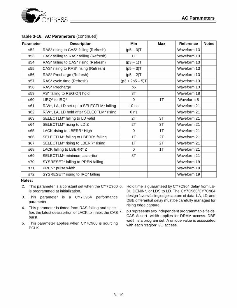
AC Parameters
3-119
Notes:
s52 RAS* rising to CAS* falling (Refresh) (p5 – 3)T Waveform 13
s53 CAS* falling to RAS* falling (Refresh) 1T Waveform 13
s54 RAS* falling to CAS* rising (Refresh) (p3 – 1)T Waveform 13
s55 CAS* rising to RAS* rising (Refresh) (p5 – 3)T Waveform 13
s56 RAS* Precharge (Refresh) (p5 – 2)T Waveform 13
s57 RAS* cycle time (Refresh) (p3 + 2p5 – 5)T Waveform 13
s58 RAS* Precharge p5 Waveform 13
s59 AS* falling to REGION hold 3T Waveform 18
s60 LIRQ* to IRQ* 0 1T Waveform 8
s61 R/W*, LA, LD set-up to SELECTLM* falling 10 ns Waveform 21
s62 R/W*, LA, LD hold after SELECTLM* rising 0 ns Waveform 21
s63 SELECTLM* falling to LD valid 2T 3T Waveform 21
s64 SELECTLM* rising to LD Z 2T 3T Waveform 21
s65 LACK rising to LBERR* High 0 1T Waveform 21
s66 SELECTLM* falling to LBERR* falling 1T 2T Waveform 21
s67 SELECTLM* rising to LBERR* rising 1T 2T Waveform 21
s68 LACK falling to LBERR* Z 0 1T Waveform 21
s69 SELECTLM* minimum assertion 8T Waveform 21
s70 SYSRESET* falling to PREN falling Waveform 19
s71 PREN* pulse width Waveform 19
s72 SYSRESET* rising to IRQ* falling Waveform 19
2. This parameter is a constant set when the CY7C960is programmed at initialization.
3. This parameter is a CY7C964 performanceparameter.
4. This parameter is timed from RAS falling and speci-fies the latest deassertion of LACK to inhibit the CASburst.
5. This parameter applies when CY7C960 is sourcingPCLK.
6. Hold time is guaranteed by CY7C964 delay from LE-DI, DENIN*, or LDS to LD. The CY7C960/CY7C964design favors falling edge capture of data. LA, LD, andDBE differential delay must be carefully managed forrising edge capture.
7. p3 represents two independent programmable fields.CAS Assert width applies for DRAM access. DBEwidth is a program set. A unique value is associatedwith each “region” I/O access.
Table 3-16. AC Parameters (continued)
Parameter Description Min Max Reference Notes
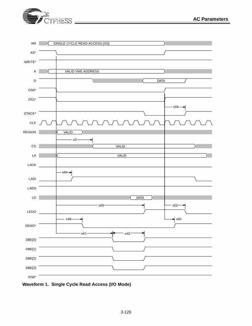
AC Parameters
3-120
Waveform 1. Single Cycle Read Access (I/O Mode)
s42
s44
s3
s40
s49 s51
s48 s50
s41
SINGLE CYCLE READ ACCESS (I/O)
VALID VME ADDRESS
DATA
VALID
DATA
VALID
VALID
AM
AS*
WRITE*
A
D
DS0*
DS1*
DTACK*
CLK
REGION
CS
LA
LACK
LADI
LAEN
LD
LEDO
DENO*
DBE[0]
DBE[1]
DBE[2]
DBE[3]
R/W*

AC Parameters
3-121
Waveform 2. Single Cycle Write Access (I/O Mode)
s42
s44
s4 s46
s45
s47
s41
SINGLE CYCLE WRITE ACCESS(I/O)
VALID VME ADDRESS
VALID
VALID
VALID
DATA
DATA
AM
AS*
WRITE*
A
D
DS0*
DS1*
DTACK*
CLK
REGION
CS
LA
LACK
LADI
LAEN
LD
LEDI
DENIN[0]*
DENIN[1]*
DBE[0]
DBE[1]
DBE[2]
DBE[3]
R/W*
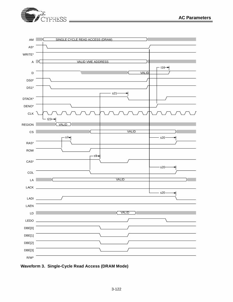
AC Parameters
3-122
Waveform 3. Single-Cycle Read Access (DRAM Mode)
t16
s21
t23
s7 s20
s9
s20
s20
SINGLE CYCLE READ ACCESS (DRAM)
VALID
VALID VME ADDRESS
VALID
VALID
VALID
VALID
AM
AS*
WRITE*
A
D
DS0*
DS1*
DTACK*
DENO*
CLK
REGION
CS
RAS*
ROW
CAS*
COL
LA
LACK
LADI
LAEN
LD
LEDO
DBE[0]
DBE[1]
DBE[2]
DBE[3]
R/W*

AC Parameters
3-123
Waveform 4. Single Cycle Write Access (DRAM Mode)
s1 s2
s22
s4
s43
s13
s25
SINGLE CYCLE WRITE ACCESS(DRAM)
VALID
VALID
VALID AME ADDRESS
VALID
VALID
VALID
AM
AS*
WRITE*
A
D
DS0*
DS1*
DTACK*
CLK
REGION
CS
RAS*
CAS*
ROW
COL
LA
LADI
LAEN
LD
DENIN[0]*
DENIN[1]*
DBE[0]
DBE[1]
DBE[2]
DBE[3]
LACK
R/W*

AC Parameters
3-124
Waveform 5. Single-Cycle Read-Modify-Write Access (I/O Mode)
t8 t2
t3
SINGLE CYCLE READ MODIFY WRITE ACCESS (I/O)
VALID VME ADDRESS
VALID
VALID
VALID
VALID VALID
VALID VALID
AM
AS*
WRITE*
A
D
DS0*
DS1*
DTACK*
CLK
REGION
CS
LA
LACK
LADI
LAEN
LD
SWDEN*
LEDO
DENO*
LEDI
DENIN[0]*
DENIN[1]*
DBE[0]
DBE[1]
DBE[2]
DBE[3]
R/W*

AC Parameters
3-125
Waveform 6. Single-Cycle Read-Modify-Write Access (DRAM Mode)
s6
s10
s29
s28
SINGLE CYCLE DRAM READ MODIFY WRITE ACCESS (DRAM)
VALID VME ADDRESS
DATA DATA
VALID
VALID
DATA DATA
VALID
AM
AS*
WRITE*
A
D
DS0*
DS1*
DTACK*
REGION
CS
ROW
RAS*
CAS*
COL
LA
LADI
LAEN
CLK
LD
LEDO
DENO*
DENIN[0]*
DENIN[1]*
DBE[0]
DBE[1]
DBE[2]
DBE[3]
LACK
R/W*

AC Parameters
3-126
Waveform 7. IACK CYCLE Self-timed
s39
s38
VALID VME ADDRESS
VALID
VALID
VALID
LIRQ
IRQ*
A
IACK*
IACKIN*
AS*
WRITE*
D
DS0*
DS1*
DTACK*
CLK
LDEN
LA
LACK
LADI
LAEN
LD
LEDO
DENO*
R/W*

AC Parameters
3-127
Waveform 8. IACK Cycle Handshake
s60
VALID VME ADDRESS
VALID
VALID
LIRQ*
IRQ*
A
IACK*
IACKIN*
AS*
WRITE*
D
DS0*
DS1*
DTACK*
CLK
LDEN*
LA
LACK
LADI
LAEN
LD
LEDO
DENO*
R/W*

AC Parameters
3-128
Waveform 9. Multiplexed Address Read-Modify-Write Access (I/O Mode)
t20 t12
s32 s33
MULTIPLEXED ADDRESS READ MODIFY WRITE ACCESS (I/O)
VALID VALID
VALID VALID
VALID
VALID
VALID
VALID
VALID
VALID
AM
AS*
WRITE*
A
D
DS0*
DS1*
DTACK*
CLK
REGION
CS
LA
LACK
LADI
LAEN
LD
SWDEN*
LEDO
DENO*
LEDI
DENIN[0]*
DENIN[1]*
DBE[0]
DBE[1]
DBE[2]
DBE[3]
R/W*

AC Parameters
3-129
Waveform 10. Multiplexed Address Read-Modify-Write Access ( DRAM Mode)
MULTIPLEXED ADDRESS READ MODIFY WRITE DRAM CYCLE
DATA
Addr.
Addr. DATA
VALID
VALID
Addr. DATA DATA
VALID
AM
AS*
WRITE*
A
D
DS0*
DS1*
DTACK*
CLK
REGION
CS
RAS*
CAS*
ROW
COL
LA
LADI
LEDI
LD
LEDO
DENO*
DENIN[0]*
DENIN[1]*
DBE[0]
DBE[1]
DBE[2]
DBE[3]
LACK
R/W*
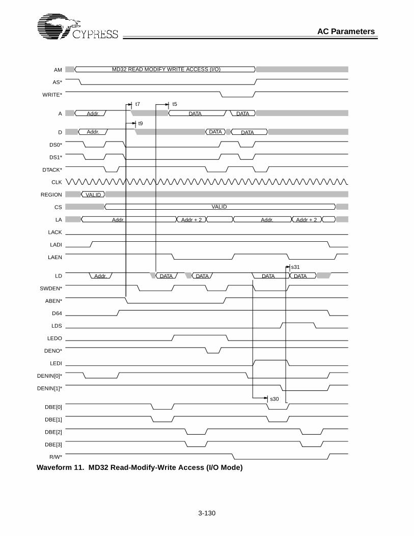
AC Parameters
3-130
Waveform 11. MD32 Read-Modify-Write Access (I/O Mode)
t7 t5
t9
s31
s30
Addr.
Addr.
VALID
VALID
Addr. Addr + 2 Addr. Addr + 2
Addr.
DATA DATA
DATA DATA
DATA DATA DATA DATA
MD32 READ MODIFY WRITE ACCESS (I/O)AM
AS*
WRITE*
A
D
DS0*
DS1*
DTACK*
CLK
REGION
CS
LA
LACK
LADI
LAEN
LD
SWDEN*
ABEN*
D64
LDS
LEDO
DENO*
LEDI
DENIN[0]*
DENIN[1]*
DBE[0]
DBE[1]
DBE[2]
DBE[3]
R/W*

AC Parameters
3-131
Waveform 12. MD32 Read-Modify-Write Access (DRAM Mode)
s18
s15
s14 s16
s17
s18
s18
s18
MD32 READ MODIFY WRITE ACCESS (DRAM)
Addr.
Addr.
VALID
VALID
Addr. Addr + 2 Addr Addr + 2
Addr. DATA DATA DATA DATA
DATA DATA
DATA DATA
AM
AS*
WRITE*
A
D
DS0*
DS1*
DTACK*
CLK
REGION
CS
RAS*
SWDEN*
CAS*
LA
ROW
COL
LADI
LAEN
LEDI
LD
LEDO
DENO*
DENIN[0]*
DENIN[1]*
ABEN*
D64
DBE[0]
DBE[1]
DBE[2]
DBE[3]
LACK
R/W*
LDS

AC Parameters
3-132
Waveform 13. Single-Cycle Write and CAS before RAS Refresh
s57s56 s58s55 s53
s52s54
SINGLE CYCLE WRITE and CAS BEFORE RAS REFRESH
VALID VME ADDRESS
DATA
VALID
VALID
VALID
DATA
AM
AS*
WRITE*
A
D
DS0*
DS1*
DTACK*
CLK
REGION
CS
RAS*
CAS*
ROW
COL
LA
LADI
LAEN
LD
DENIN[0]*
DENIN[1]*
DBE[0]
DBE[1]
DBE[2]
DBE[3]
LACK
R/W*

AC Parameters
3-133
Waveform 14. Block Transfer Read (Slow VME)
s23
BLOCK TRANSFER READ (SLOW VMEbus)
Addr.
DATA DATA DATA
VALID
VALID
Addr Addr + 2 Addr + 4 Addr + 6
DATA DATA DATA DATA
AM
AS*
WRITE*
A
D
DS0*
DS1*
DTACK*
CLK
REGION
CS
LA
LACK
LADI
LAEN
LD
SWDEN*
LEDO
DENO*
DBE[0]
DBE[1]
DBE[2]
DBE[3]
R/W*
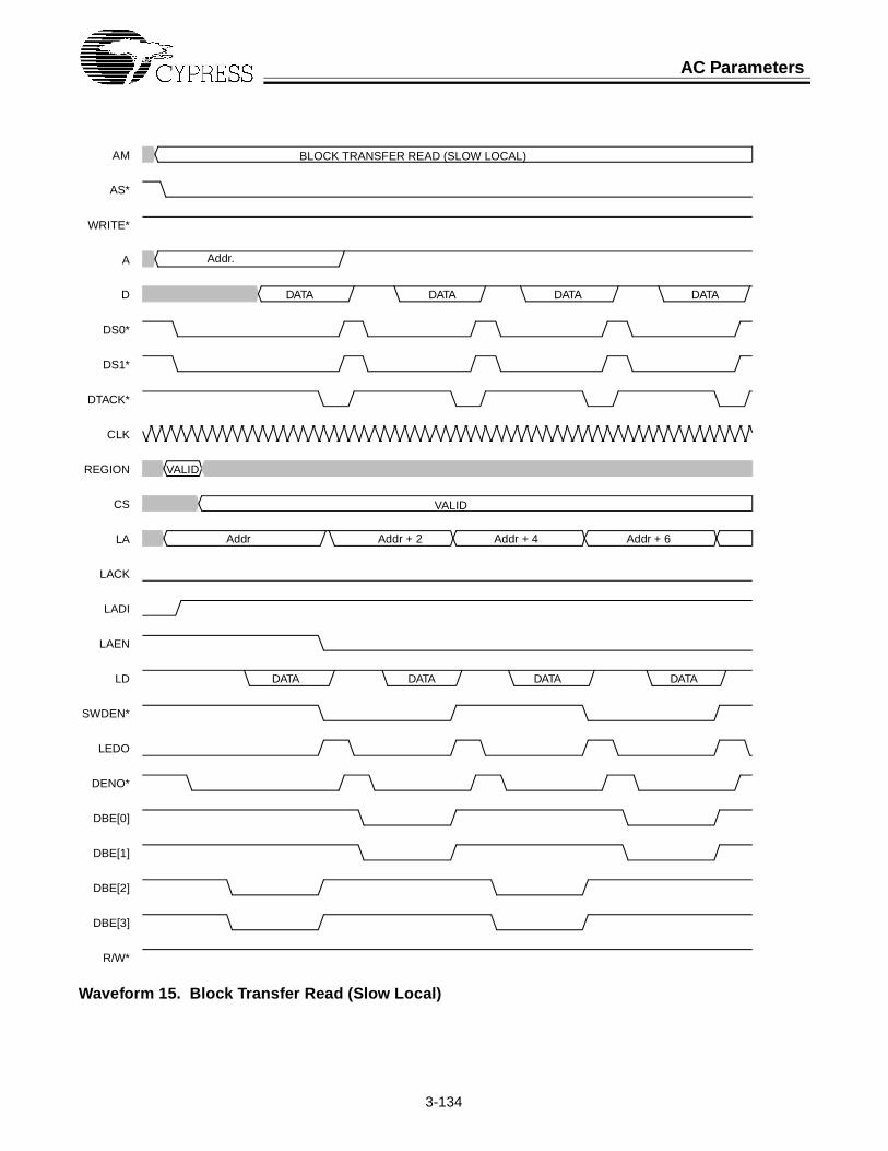
AC Parameters
3-134
Waveform 15. Block Transfer Read (Slow Local)
BLOCK TRANSFER READ (SLOW LOCAL)
Addr.
DATA DATA DATA DATA
VALID
VALID
Addr Addr + 2 Addr + 4 Addr + 6
DATA DATA DATA DATA
AM
AS*
WRITE*
A
D
DS0*
DS1*
DTACK*
CLK
REGION
CS
LA
LACK
LADI
LAEN
LD
SWDEN*
LEDO
DENO*
DBE[0]
DBE[1]
DBE[2]
DBE[3]
R/W*

AC Parameters
3-135
Waveform 16. Block Transfer Write (Slow VMEbus)
s24
BLOCK TRANSFER WRITE (SLOW VMEbus)
Addr.
DATA DATA DATA DATA
VALID
VALID
Addr Addr + 2 Addr + 4 Addr + 6
DATA DATA DATA DATA
AM
AS*
WRITE*
A
D
DS0*
DS1*
DTACK*
CLK
REGION
CS
LA
LACK
LADI
LAEN
LD
SWDEN*
LEDI
DENIN[0]*
DENIN[1]*
DBE[0]
DBE[1]
DBE[2]
DBE[3]
R/W*

AC Parameters
3-136
Waveform 17. Block Transfer Write (Slow Local)
Addr.
DATA DATA DATA DATA DATA
VALID
VALID
Addr Addr + 2 Addr + 4 Addr + 6
DATA DATA DATA DATA
BLOCK DATA TRANSFER WRITE (SLOW LOCAL)AM
AS*
WRITE*
A
D
DS0*
DS1*
DTACK*
CLK
REGION
CS
LA
LACK
LADI
LAEN
LD
SWDEN*
LEDI
DENIN[0]*
DENIN[1]*
DBE[0]
DBE[1]
DBE[2]
DBE[3]
R/W*

AC Parameters
3-137
Waveform 18. AMCODE or LA and Decode Timing
s5s59
t138
t11 t19
VALID AM CODE
VALID VME ADDRESS
VALID LOCAL ADDRESS [31:8]
VALID LOCAL ADDRESS [7:0]AM CODE
VALID
VALID
AM
AS*
A
DS0*
DS1*
DTACK*
CLK
REGION
LADI
LA[31:8]
LAEN
LA[7:0]
CS
RAS*
ROW

AC Parameters
3-138
Waveform 19. VMEbus Initialization Method
s71
s70
s72
CR/CSR
CR/CSR CR/CSR
CR/CSR
SYSRESET*
PREN*
IRQ*
AM
A
WRITE*
IACK*
AS*
DS1*
DTACK*
LAEN

AC Parameters
3-139
Waveform 20. Block Transfer Write (DRAM Mode)
s19
t4
VALID
REV ”C” Block Transfer
DATA DATA DATA DATA
VALID VALID VALID
DATA DATA DATA DATA
VALID
VALID
VALID
AM
AS*
WRITE*
A
D
DS0*
DTACK*
CLK
LADI
LA
LAEN
REGION
CS
DENIN[0]*
LD
LEDI
RAS*
CAS*
R/W*

AC Parameters
3-140
Waveform 21. Local Bus Holdoff (and CY7C961 Register Access)
s69
s62
s61
s63 s64
s65 s66 s67 s68
DATA from CY7C961
Register AddressAM AM
VALID
DATA to CY7C961/CY7C964
CLK
LADI
R/W*
LAEN
LA[4:2]
LD(write)
SELECTLM*
LD(read)
LBERR*
LACK

AC Parameters
3-141
Waveform 22. D64 Block Read Access (DRAM Mode)
t25t26
t28t29
t15
t17
D64 BLOCK READ ACCESS (DRAM MODE)
Addr.
VALID
AM CODE
data data data data data data
Addr Addr + 4 Addr + 8 Addr + 12 Addr + 16 Addr + 20
DATA DATA DATA
DATADATA
VALID
AM
AS*
WRITE*
A
D
DS0*
DS1*
DTACK*
CLK
REGION
CS
RAS*
CAS*
ROW
COL
LA
LADI
LAEN
LACK
ABEN*
LD
LEDO
DENO*
D64
DBE[0]
DBE[1]
DBE[2]
DBE[3]
R/W*

AC Parameters
3-142
Waveform 23. D64 Block Write Access (DRAM Mode)
t37t38
t13 t74 t75
D64 BLOCK WRITE ACCESS (DRAM MODE)
ADDR DATA DATA DATA
DATA DATA DATA
ADDR ADDR + 4 ADDR + 8 ADDR + 12 ADDR + 16AM CODE
DATA DATA DATA DATA DATA
VALID
VALID
AM
AS*
WRITE*
A
D
DS0*
DS1*
DTACK*
CLK
REGION
CS
RAS*
CAS*
ROW
COL
LA
LADI
LAEN
LEDI
LD
DENIN[0]*
DENIN[1]*
ABEN*
D64
DBE[0]
DBE[1]
DBE[2]
DBE[3]
LDS
R/W*

AC Parameters
3-143
Waveform 24. LACK Handshake (I/O Mode)
Waveform 25. LACK Handshake (DRAM Mode)
s27
s26
VALID
VALID
AM
AS*
CS
SWDEN*
DBE[0]
DBE[1]
LACK
DBE[2]
DBE[3]
s12
s11
1 or 0 1 or 0
AS*
DS1*
DTACK*
CLK1
CS
RAS*
CAS*
ROW
COL
DBE[0]
LACK

AC Parameters
3-144
Waveform 26. Local Initialization Method
s34s8
s35 s37 s36
Serial DATA from PROM
SYSRESET*
PREN*
PCLK
PDATA
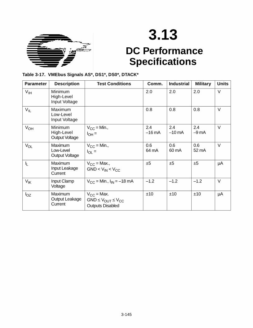
3-145
3.13 DC Performance
SpecificationsTable 3-17. VMEbus Signals AS*, DS1*, DS0*, DTACK*
Parameter Description Test Conditions Comm. Industrial Military Units
VIH MinimumHigh-LevelInput Voltage
2.0 2.0 2.0 V
VIL MaximumLow-LevelInput Voltage
0.8 0.8 0.8 V
VOH MinimumHigh-LevelOutput Voltage
VCC = Min.,IOH =
2.4–16 mA
2.4–10 mA
2.4–9 mA
V
VOL MaximumLow-LevelOutput Voltage
VCC = Min.,IOL =
0.664 mA
0.660 mA
0.652 mA
V
IL MaximumInput LeakageCurrent
VCC = Max.,GND < VIN < VCC
±5 ±5 ±5 µA
VIK Input ClampVoltage
VCC = Min., IIN = –18 mA –1.2 –1.2 –1.2 V
IOZ MaximumOutput LeakageCurrent
VCC = Max.GND < VOUT < VCCOutputs Disabled
±10 ±10 ±10 µA

Introduction to the VIC068A
3-146
Table 3-18. VMEbus Signals AM5, AM4, AM3, AM2, AM1, AM0, IRQ*, BERR* [1]
Note:
1. The BERR* signal has an on-chip pull-up resistor. For this signal the IOZ value is modified by Table 3-21.
Parameter Description Test Conditions Comm. Industrial Military Units
VIH MinimumHigh-LevelInput Voltage
2.0 2.0 2.0 V
VIL MaximumLow-LevelInput Voltage
0.8 0.8 0.8 V
VOH MinimumHigh-LevelOutput Voltage
VCC = Min.,IOH =
2.4–16 mA
2.4–10 mA
2.4–9 mA
V
VOL MinimumLow-LevelOutput Voltage
VCC = Min.,IOL =
0.648 mA
0.644 mA
0.638 mA
V
IL MaximumInput LeakageCurrent
VCC = Max.,GND < VIN < VCC
±5 ±5 ±5 µA
VIK Input ClampVoltage
VCC = Min., IIN = –18 mA –1.2 –1.2 –1.2 V
IOZ MaximumOutput LeakageCurrent
VCC = Max.GND < VOUT < VCCOutputs Disabled
±5 ±5 ±10 µA

Introduction to the VIC068A
3-147
Table 3-19. All Other Output Signals [2]
Note:
2. Some signals have an on-chip pull-up or pull-down resistors. For these signals IOZ value is modified.
Table 3-20. Capacitance - All Signals
Table 3-21. Pullup/Pulldown Current - All Signals
Table 3-22. Operating Current (CY7C960/CY7C961)
Parameter Description Test Conditions Comm. Industrial Military Units
VIH MinimumHigh-LevelInput Voltage
2.0 2.0 2.0 V
VIL MaximumLow-LevelInput Voltage
0.8 0.8 0.8 V
VOH MinimumHigh-LevelOutput Voltage
VCC = Min.,IOH =
2.4–16 mA
2.4–10 mA
2.4–9 mA
V
VOL MinimumLow-LevelOutput Voltage
VCC = Min.,IOL =
0.620 mA
0.618 mA
0.616 mA
V
IL MaximumInput LeakageCurrent
VCC = Max.,GND < VIN < VCC
±5 ±5 ±5 µA
VIK Input ClampVoltage
VCC = Min., IIN = –18 mA –1.2 –1.2 –1.2 V
IOZ MaximumOutput LeakageCurrent
VCC = Max.GND < VOUT < VCCOutputs Disabled
±5 ±5 ±10 µA
Parameters Description Test Conditions Max. Units
CIN Input Capacitance TA = 25°C, f = 1 MHz,VCC = 5.0V
10 pF
COUT Output Capacitance 10 pF
Parameters Description Test Conditions Typ. Max.
IPU Input PullupCurrent
TA =–55°C, VCC = 5.5VVIN = GND
100 mA 250 µA
IPD Input PulldownCurrent
TA = –55°C, VCC = 5.5VVIN = VCC
–100 mA –250 µA
Parameters Description Test Conditions Max. Units
IDD Maximum Operating Current
No external DC load 100 mA
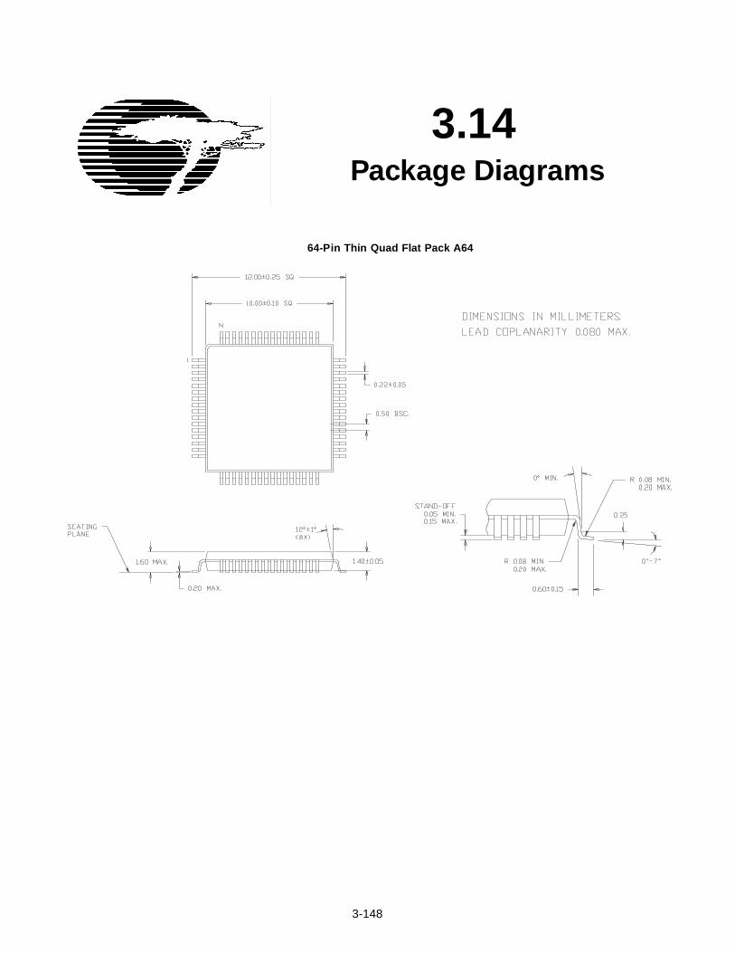
3-148
3.14 Package Diagrams
64-Pin Thin Quad Flat Pack A64

Package Diagrams
3-149
100-Pin Plastic Thin Quad Flat Pack (TQFP) A100
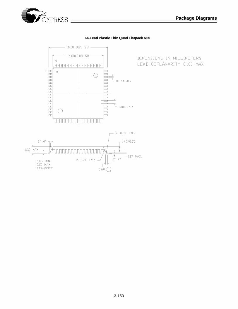
Package Diagrams
3-150
64-Lead Plastic Thin Quad Flatpack N65

Section 4
The CY7C964 Bus
Interface Logic Circuit

4-4
4.1 Introduction
The CY7C964 is a flexible collection of byte (8-bit) wide transceivers, latches, counters,multiplexers, and comparators that provide bus interface designs with a low-cost alternativeto PLDs, ASICs, or discrete logic devices. It is based on a standard cell design that incorpo-rates patented line drivers for reduced ground bounce and high noise immunity. The CY7C964is a companion part to Cypress’s VIC068A, VIC64, CY7C960, and CY7C961 VMEbus inter-face controller devices. It is completely compatible with all operating modes of these devices,such as dual-address path, block transfer boundary crossing conditions, block transfer initial-ization cycle, local DMA control, and D64 VMEbus block transfers. Signal-naming conventionscorrespond directly to the VIC068A/VIC64/CY7C960/961 buffer control signals, and theCY7C964 can be directly connected to these corresponding signals.
The CY7C964 can also be used as a generic-interface building block. Some examples includelow-cost slave VMEbus controllers, VSB interfaces, or other interface applications. CY7C964sare cascadable, allowing easy interfacing to buses of any width. By combining multiple logicfunctions into one discrete part, the CY7C964 saves board space and reduces power con-sumption, which is becoming increasingly important to designers.

4-5
4.2 Features
• Directly connects to VIC068A, VIC64, CY7C960, or CY7C961
• Has internal counters for block transfer and local DMA address control
• Has internal multiplexers for D64 64-bit VMEbus block transfers
• Has internal comparators for address decoding
• Supports VIC068A/VIC64 dual-address-path option
• Has cascadable operation
• Directly drives VMEbus address and data bus signals
• Directly drives local address and data bus signals
• Reduces components for a compact board design
• Has low power requirements
• Is available in a 64-pin TQFP or 68-pin PGA

4-6
4.3 Interfacing to Cypress
VMEbus Interface Controllers
Previously, interfacing the VIC068A to the VMEbus required a significant number of LSI andMSI devices. With the advent of 64-bit VMEbus block transfers and the VIC64, the externaldiscrete device count for a full functional interface has expanded. The CY7C964 has beendeveloped to combat this problem by incorporating the functions of much of this external logicinto a single package. Using the CY7C964 shortens system design, debug, and manufacturingcycle times. Design engineers are relieved from the burden of performing critical or worst-case timing analysis on the VMEbus and VIC buffer control signals. Local control signalsother than those directly interfaceable to the interface controllers have been kept to a minimum.
A full function D64 VMEbus interface implemented using the CY7C964, VIC64, and all VME-bus interface local support logic includes the following features:
• block transfer support for D16, D32, and D64 VMEbus transfers
• dual-path address operation (allowing single-cycle transfers during master block transferinterleave periods)
• slave block transfers during master block transfer interleave periods
• fully programmable slave VMEbus address decoding
• write posting
• the VIC mail box interrupt message support
The interface can be broken into five functional sections for the purpose of discussion. Thesesections are:
• VMEbus signal group
• Buffer control signal group
• CY7C964 local signal group
• CY7C964 address comparator and local signal group
• Local data swap buffer logic
The focus of this section is the CY7C964. Each of the interface functional blocks are examinedfrom this perspective. For additional information on the signals described within this section,consult the VMEbus Specification (IEEE 1014) and/or the section of this book that describesthe controller you are connecting.
4.3.1 VMEbus Signal Group
This group includes the VMEbus address and data signals. Each CY7C964 provides supportfor 8 bits of VMEbus address and data. Three CY7C964s are necessary for 32-bit interface

Interfacing to Cypress VMEbus Interface Controllers
4-7
applications when used with the VIC068A or VIC64. Four CY7C964s are used with CY7C960and CY7C961 for full-function slave interfaces. The A[7:0] and D[7:0] transceivers on theCY7C964 furnish a high drive strength, allowing direct connection to the respective addressand data signals on the VMEbus backplane. With any of Cypress’s family of VMEbus interfacecontrollers generating the control information, the CY7C964s meet VMEbus worst-case timingand drive-strength requirements for all forms of data transfers.
Table 4-1. VMEbus Signals
4.3.2 Buffer Control Signal Group
This group includes all of the address and data buffer control signals. A major design timesavings is realized using the CY7C964s as all of these signals directly connect to the chosencontroller or are wired to a steady state value. The buffer control interface is simple andstraightforward with a few minor exceptions. Table 4-2 specifies these connections for theVIC068A and VIC64 controllers.
Signal Description Interface Comments
D[7:0] VMEbus compatible data signals Directly connect to VMEbus P1 and P2 connectors
A[7:0] VMEbus compatible address signals Directly connect to VMEbus P1 and P2 connectors
Table 4-2. Buffer Control Signals Connection for VIC068A and VIC64
Signal Description Interface Comments
LADO Latch address out Directly connect to VIC LADO on all CY7C964s
LADI Latch address in Directly connect to VIC LADI on all CY7C964s
LEDO Latch enable data out Directly connect to VIC LEDO on all CY7C964s
LEDI Latch enable data in Directly connect to VIC LEDI on all CY7C964s
ABEN* VMEbus address bus enable Directly connect to VIC ABEN* on all CY7C964s
DENO* Data enable output Directly connect to VIC DENO* on all CY7C964s
D64 D64 block transfer mode enable Directly connect to VIC64 SCON/D64 pin on all CY7C964s. Tie this input LOW on all CY7C964s when using VIC068A.
BLT* Block transfer enable Directly connect to VIC BLT* on all CY7C964s
LAEN Local address enable Directly connect to VIC LAEN on all CY7C964s
DENIN* Primary data enable in signal Directly connect to VIC DENIN1* on NMSB and MSB CY7C964s, directly connect to VIC DENIN* on LSB CY7C964
DENIN1* Companion data enable in signal Directly connect to VIC DENIN* on NMSB and MSB CY7C964s, directly connect to VIC DENIN1* on LSB CY7C964

Interfacing to Cypress VMEbus Interface Controllers
4-8
4.3.3 CY7C964 Local Signal Group
The CY7C964 local signal group consists of the VMEbus and local block-transfer countercount-enable daisy-chains. These signals enable the local and VMEbus higher-order addresscounters; two local address counters (a master block transfer and a slave block transfer) anda single VMEbus address counter. The local address counters share the LCIN*/LCOUT*count-enable daisy-chain. These signals are multiplexed within the CY7C964 and enablecounting for the proper counter depending on the current state of the interface. The VCIN*/VCOUT* daisy-chain is dedicated to the VMEbus address counter on the device. When theVCIN* or LCIN* are held Low, counting is enabled for the appropriate counters within thedevice. The VCIN* or LCIN* signals do not advance the counters, they just enable counting.The counters increment when these signals are active and the proper increment count controllogic sequence occurs. The controller advances the address counters at the proper timeduring VMEbus and local DMA block transfer operations. For further information on the counteradvance control sequence, refer to Chapter 4.5, CY7C964 Operation.
Table 4-3. CY7C964 Local Signals for VIC068A and VIC64
4.3.4 CY7C964 Address Comparison and Local Signal Group
The implementation of this group of CY7C964 signals is application specific. The MWB* signaland FC1 signal have been included in this section because they are locally generated signalsrequired by the VIC and output directly from the CY7C961. These two signals differ slightlyon the VIC; MWB* is an input only, while FC1 is a bidirectional signal that can be driven by
Signal Description Interface Comments
LCIN* Local address counter count enable On LSB CY7C964, tie this input Low. On the NMSB device, directly connect to the LCOUT* of the LSB device. For the MSB CY7C964, connect to the LCOUT* of the NMSB device.
LCOUT* Local address counter carry out On LSB CY7C964, connect this output to the LCIN* input. On the NMSB CY7C964, connect this output to the MSB LCIN* input. For the MSB device do not connect this output.
VCIN* VMEbus address counter count enable
On LSB CY7C964, tie this input Low. On the NMSB device, directly connect to the VCOUT* of the LSB device. For the MSB CY7C964, connect to the VCOUT* of the NMSB device.
VCOUT* VMEbus address counter carry out On LSB CY7C964, connect this output to the VCIN* input. On the NMSB CY7C964, connect this output to the MSB VCIN* input. For the MSB device do not connect this output.

Interfacing to Cypress VMEbus Interface Controllers
4-9
the VIC. On the CY7C964 the MWB* and FC1 signals are inputs. These signals should bedirectly connected to the respective local signals on VIC or CY7C961. For CY7C960 designs,MWB* should be connected to VCC and FC1 should be connected to GND.
The CY7C964s contain a high-performance programmable VMEbus address equality com-parator. The comparator is controlled by two internal, write-only registers: a mask and acompare register. The mask register enables and disables bits of the comparator, and thecompare register stores the data pattern that inputs are compared against. VCOMP* is theactive-Low comparator match output signal. VCOMP* is driven Low by the CY7C964 whenthe bit pattern on pins A[7:0] match enabled bits of the compare register. Setting mask registerbits to 0 enables the corresponding bits of the compare register. Loading bits of the maskregister with 1s places bits of the compare register in don’t care or “match anything” state.Loading the mask register with all 0s forces the compare register to match all bits of the patternon A[7:0]. Setting the mask register to all 1s effectively disables the on-board comparator.VCOMP* will always be Low.
These registers are loaded by supplying the proper data on LD[7:0] and the register addresson MWB* and LDS signals. The STROBE input is used to qualify the address and latch thedata into the proper internal register. Figure 4-1 and Figure 4-2 show the waveforms needed toload the compare and mask registers.
This load cycle operates as follows:
1. The state of LDS and MWB* are latched on the falling edge of STROBE.
2. The data is loaded into the selected register on the rising edge of the STROBE signal.
3. MWB* must be held inactive (High): the state of LDS selects the register to load.
4. If LDS is High at the falling edge of STROBE, the compare register will be loaded; if LDSis Low the data is written to the mask register.
Table 4-4. CY7C964 Address Comparison and Local Signals for VIC068A and VIC64
Signal Description Interface Comments
FC1 Function code 1 signal Directly connect on all CY7C964s to the same local signal that drives the FC1 signal on the VIC.
MWB* Module wants VMEbus Directly connect on all CY7C964s to the same local signal that drives the MWB* signal on the VIC.
LDS Load register select signal Should be directly connected to LA2 for VIC sys-tems with 32-bit local bus. Refer to text below for further information.
STROBE Latch register control signal Chip select-like signal for CY7C964 internal comparator mask and comparison registers. See text below for further information.
VCOMP* VMEbus address comparator output Needs a small amount of external glue logic to validate an combine signals in a parallel high-performance fashion.

Interfacing to Cypress VMEbus Interface Controllers
4-10
Figure 4-1. Mask Register Load Timing
Figure 4-2. Compare Register Load Timing
This load cycle can be generated by decoding a separate address region or chip select signalfor the CY7C964 comparator registers. In applications with a 32-bit local bus, it is desirableto load all three CY7C964s in parallel by having the host processor perform a 32-bit writecycle to the address region that will activate STROBE. The select signal for the address regionis connected to the STROBE input on all CY7C964s. Boards that implement VIC068A orVIC64 interface should connect LDS to LA2, thereby decoding the mask register at the baseaddress of the address region and the compare register at the base address + 4. LDS also controlsthe operation of the D64 block transfer data multiplexer/demultiplexer. If it is not connected to LA2,this logic will not operate properly. For CY7C960 and CY7C961 designs, LDS is connected directlyto the controller.
t43 t44
t47
t45 t46
Load CY7C964 Mask Register
MWB*
LDS
STROBE
LD[7:0] Data Valid
t43 t44
t47
t45 t46
Load CY7C964 Compare Register
MWB*
LDS
STROBE
LD[7:0] Data Valid

Interfacing to Cypress VMEbus Interface Controllers
4-11
The mask and compare registers can be set to select any contiguous address region on theVMEbus. These registers do not preload and therefore power up in an unknown state. It isadvisable to initialize these registers as soon as possible in the system boot sequence. Notethat the act of writing the compare register clears the mask register.
The CY7C964 comparator output signal VCOMP* supplies the result from the equality com-pare logic. VCOMP* drives Low when the input matches the loaded conditions. The CY7C964VCOMP* signals are not directly compatible with the VIC SLSEL0* and SLSEL1* slave selectsignals. The short (10 ns) address set-up time to AS* active for VMEbus slave boards doesnot meet the worst case compare out delay of the CY7C964 VCOMP* signal. combining thiswith the potential output glitching that can occur with an asynchronous comparator can causeproblems for the VIC. It is recommended that the VCOMP* signal be externally filtered priorto being used with the VIC SLSEL0* or SLSEL1* signal. Most applications will require someexternal comparison logic to combine VCOMP* signals from the NMSB and MSB device,furnishing finer grained VMEbus decoding: this logic can also be used to filter the CY7C964VCOMP* signals. Note that CY7C960 and CY7C961 have a built-in decode delay feature,which eliminates the need for external filtering.
4.3.5 Local Data Swap Buffer Logic
Local Data Swap Buffer logic is a requirement for all 32-bit local bus designs that perform 8-or 16-bit transfers. The swap buffer moves data to and from the lower section of the VMEbus,D[15:0], to the upper segments of the local bus, D[31:16]. VMEbus requires that all 8- and16-bit data transfers be performed on the D[15:0] section of the bus. The CY7C964s workproperly with the VIC-controlled or CY7C960/961-controlled swap buffer. For the VIC case,if an isolation buffer is implemented, care should be taken to ensure that the local data busis driven to the least-significant CY7C964 during address/mask register programming cycles.One way to ensure this is to assert the CS* and PAS* signals to the VIC068/VIC64, thuscausing VIC to assert the ISOBE* signal to the isolation buffer.

4-12
4.4 Signal Descriptions
4.4.1 VMEbus Signals
A[7:0]
Input: YesOutput: Yes, three-stateDrive: 48 mA
These are VMEbus-compatible address signal transceivers that can be directly connected tothe VMEbus. A0 is the least-significant address bit. In flow-through modes of operation, thesesignals correspond one for one with local interface signals LA[7:0].
In VMEbus interface applications, including those using the VIC068A, VIC64, CY7C960, orCY7C961, these signals should be connected to the VMEbus address bus sequentially.
In CY7C960/961 designs, A0 on the least-significant CY7C964 should be connected to theVMEbus LWORD* signal.
D[7:0]
Input: YesOutput: Yes, three-stateDrive: 48 mA
These are VMEbus-compatible data signal transceivers that can be directly connected to theVMEbus. D0 is the least-significant data bit. In flow-through modes of operation, these signalscorrespond one for one with local interface signals LD[7:0].
In VMEbus interface applications, including those using the VIC068A, VIC64, CY7C960, orCY7C961, these signals should be connected to the VMEbus data bus sequentially.
4.4.2 Local Signals
LA[7:0]
Input: YesOutput: Yes, three-stateDrive: 8 mA
These are medium drive-strength local address transceivers that allow direct connection tomemory, microprocessors and/or peripheral controllers. LA0 is the least-significant local ad-dress signal. In flow-through operating modes, these signals correspond one for one with theVMEbus signals A[7:0].

Signal Descriptions
4-13
When implementing conventional VMEbus interfaces or using the CY7C964 with theVIC068A, VIC64, CY7C960, or CY7C961, these signals should be connected to the localaddress bus sequentially.
LD[7:0]
Input: YesOutput: Yes, three-stateDrive: 8 mA
These are medium drive-strength local data transceivers that allow direct connection to mem-ory, microprocessors and/or peripheral controllers. LD0 is the least-significant local data sig-nal. In flow-through operating modes, these signals correspond one for one with the VMEbussignals D[7:0].
When implementing conventional VMEbus interfaces or using the CY7C964 with theVIC068A, VIC64, CY7C960, or CY7C961, these signals should be connected to the localdata bus sequentially.
ABEN*
Input: YesOutput: No
This is the VMEbus Address Bus ENable control signal. This signal controls the state of theVMEbus address transceivers A[7:0]. When asserted (driven Low), the transceivers are con-figured as outputs and are enabled.
When using the CY7C964 with the VIC068A, VIC64, CY7C960, or CY7C961 to implementVMEbus interfaces, this input should be connected to the ABEN* output of the controller.
BLT*
Input: YesOutput: No
This signal controls the VIC-compatible block transfer operations that require local DirectMemory Access (DMA). If this input is driven Low, the CY7C964 will operate in the appropriateVIC-compatible block transfer mode (dependent on the states of the other buffer control logic).
When using the CY7C964 with the VIC068A, VIC64, or CY7C961, this signal can be directlyconnected to the controller BLT* pin. A rising edge of BLT* increments the local addresscounters if LCIN* is Low. Refer to the LCIN* signal description and Chapter 4.5, CY7C964Operation, for the further information on the local address counter function.

Signal Descriptions
4-14
D64
Input: YesOutput: No
This signal is used to indicate to the CY7C964 that a VMEbus D64 block transfer is in progress.When High, the CY7C964 is instructed to use the high-performance two-state pipeline andmultiplex or demultiplex 64-bit data to and from the VMEbus address bus.
When used in conjunction with the VIC64, CY7C960, or CY7C961, this pin can be directlyconnected to the SCON*/D64 signal. For applications that only support 32-bit block transfers,as is the case with the VIC068A, this input should be tied Low.
DENIN*
Input: YesOutput: No
The Data ENable IN signal is used to control the three-state data transceivers LD[7:0]. If alogic Low level is presented to this input, LD[7:0] transceivers will be enable. In conventionalVMEbus designs, this signal would need to be driven during master read or slave writeoperations.
When used in conjunction with the VIC068A, VIC64, CY7C960, or CY7C961, this input istypically connected to DENIN1* for CY7C964’s controlling bus data lines D16 through D31,and DENIN* for the CY7C964’s controlling bus data lines D8 through D15.
DENIN1*
Input: YesOutput: No
The Data ENable IN 1 signal is used in conjunction with DENIN* to latch data from the VMEbusand provide a second enable control of the LD[7:0] transceivers for D64 transactions.
When used in conjunction with VIC64, CY7C960, or CY7C961, this input is typically connectedto DENIN* for CY7C964’s controlling bus data signals D16 through D31, and DENIN1* forthe CY7C964’s controlling bus data signals D8 through D15.
DENO*
Input: YesOutput: No
The Data ENable Out signal is used to control the three-state transceivers D[7:0]. If a logic-Low level is presented to this input, the D[7:0] transceivers will be enabled. In conventionalVMEbus design, the D[7:0] signals will be directly connected to the VMEbus. Used in thismanner, this input must be asserted during master writes and slave read operations.
When used in conjunction with the VIC068A, VIC64, CY7C960, or CY7C961, this signalshould be connected to the DENO* output on the controller.

Signal Descriptions
4-15
FC1
Input: YesOutput: No
The Function Code 1 input is used by the CY7C964 during block transfer operations todetermine the source for the local address signals LA[7:0]. If the input is driven High, theinternal Local DMA counter is selected as the source for LA[7:0]. If this input is Low, the SlaveBlock Transfer counter is the source for LA[7:0].
When used with the VIC068A, VIC64, or CY7C961, this signal can be directly connected tothe FC1 pin of the controller. The controller will drive this pin to the proper level for slave orblock transfer operations when it is master of the local system bus.
When used with the CY7C960, this signal should be tied to GND.
LCOUT*
Input: NoOutput: YesDrive: 8 mA
The Local Carry Out signal is used by the CY7C964 for cascading the local address counterchains. This signal will drive Low when the local address counter has reached the maximumcount (255). The signal generates a synchronous count enable for the next-most-significantCY7C964 in the cascade chain. This signal alone does not cause the local address counterto increment.
When cascading the CY7C964s, this signal should be connected to the LCIN* pin of the nextmost significant device. Refer to the description of the LCIN* pin for further information on theoperation of the local address counters.
LDS
Input: YesOutput: No
The Local Data Select input has two main functions: (1) as a control input for the data toaddress bus multiplexer during D64 VMEbus block transfers, (2) as a select bit for configuringthe CY7C964 address comparison and mask registers. Refer to Chapter 4.5, CY7C964 Op-eration, for further information about how data is steered to and from the VMEbus addressbus during block transfers. Typically this input will be connected to LA2 for VIC controllers andto the LDS output of CY7C960/961.
When configuring the CY7C964 internal address mask and address compare registers, thispin in conjunction with MWB* selects which registers to load. During a comparator registerload cycle, LDS High will select the Address Compare register; otherwise the Address Maskregister will be selected.

Signal Descriptions
4-16
LADI
Input: YesOutput: No
The Latch ADdress In signal controls a transparent VMEbus to local address latch within theCY7C964. When this input is High, the device will latch the data present on A[7:0]. Thisfunction is useful when building VMEbus interfaces for latching the VMEbus address duringa slave access. If LADI is Low, the internal address latch will be in a flow-through mode. LADIis also used to increment the slave block transfer local address counter. LADI is used inconjunction with LAEN to control the operation of the VMEbus to local address section of theCY7C964. For more information, refer to the description of LAEN.
When using the CY7C964 to implement VMEbus interfaces, this signal is used to maintainthe local address during slave read and write cycles. For VMEbus designs that use a Cypresscontroller, this input should be connected to the LADI output of the controller.
LAEN
Input: YesOutput: No
The Local Address ENable signal controls the three-state enable for signals LA[7:0]. Whenthis signal is High, LA[7:0] drive the address local bus. Driving the signal Low places LA[7:0]in the high-impedance/input state.
When using the CY7C964 to implement VMEbus interfaces, this signal is driven High tomaintain the local address VMEbus during slave cycles. For VMEbus interfaces using theVIC068A or VIC64, this pin should be connected to the LAEN output on the VIC. For CY7C960/961 designs, only the least-significant CY7C964 is connected to the LAEN output of thecontroller.
LEDI
Input: YesOutput: No
The Latch Enable Data In signal controls a transparent VMEbus-to-local-data-bus latch withinthe CY7C964. When this input is High, the device will latch the data present on D[7:0]. Thisfunction is useful when building VMEbus interfaces for latching the VMEbus data during amaster or slave access. If LEDI is Low, the internal address latch will be in a flow-through mode.
LEDI is used in conjunction with DENIN* and DENIN1* to control the operation of the addressVMEbus-to-local-data section of the CY7C964.
When implementing VMEbus interfaces with the CY7C964, LEDI can be used to maintain thelocal data during VMEbus master read and slave write cycles. For VMEbus designs that usea Cypress controller, this input should be connected to the LEDI output of the controller.
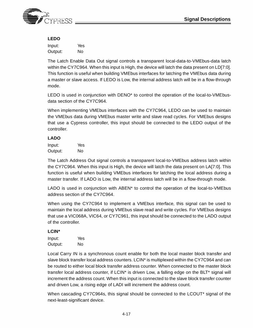
Signal Descriptions
4-17
LEDO
Input: YesOutput: No
The Latch Enable Data Out signal controls a transparent local-data-to-VMEbus-data latchwithin the CY7C964. When this input is High, the device will latch the data present on LD[7:0].This function is useful when building VMEbus interfaces for latching the VMEbus data duringa master or slave access. If LEDO is Low, the internal address latch will be in a flow-throughmode.
LEDO is used in conjunction with DENO* to control the operation of the local-to-VMEbus-data section of the CY7C964.
When implementing VMEbus interfaces with the CY7C964, LEDO can be used to maintainthe VMEbus data during VMEbus master write and slave read cycles. For VMEbus designsthat use a Cypress controller, this input should be connected to the LEDO output of thecontroller.
LADO
Input: YesOutput: No
The Latch Address Out signal controls a transparent local-to-VMEbus address latch withinthe CY7C964. When this input is High, the device will latch the data present on LA[7:0]. Thisfunction is useful when building VMEbus interfaces for latching the local address during amaster transfer. If LADO is Low, the internal address latch will be in a flow-through mode.
LADO is used in conjunction with ABEN* to control the operation of the local-to-VMEbusaddress section of the CY7C964.
When using the CY7C964 to implement a VMEbus interface, this signal can be used tomaintain the local address during VMEbus slave read and write cycles. For VMEbus designsthat use a VIC068A, VIC64, or CY7C961, this input should be connected to the LADO outputof the controller.
LCIN*
Input: YesOutput: No
Local Carry IN is a synchronous count enable for both the local master block transfer andslave block transfer local address counters. LCIN* is multiplexed within the CY7C964 and canbe routed to either local block transfer address counter. When connected to the master blocktransfer local address counter, if LCIN* is driven Low, a falling edge on the BLT* signal willincrement the address count. When this input is connected to the slave block transfer counterand driven Low, a rising edge of LADI will increment the address count.
When cascading CY7C964s, this signal should be connected to the LCOUT* signal of thenext-least-significant device.

Signal Descriptions
4-18
MWB*
Input: YesOutput: No
The Module Wants Bus is a decoding/control signal for the CY7C964 that allows the deviceto discern the cycle type. When MWB* is active (Low), the CY7C964 assumes that a blocktransfer initiation cycle or a single-cycle VMEbus transfer is pending. Subsequent assertionof BLT* allows the CY7C964 to enter block transfer mode.
MWB* is also used to decode accesses to the CY7C964 address Mask and Compare regis-ters. To load these registers, MWB* must be inactive (High).
STROBE
Input: YesOutput: No
The STROBE signal controls the loading of the internal Address Mask and Compare registers.This signal operates in the same manner as an active-Low chip select for these registers.When STROBE is Low and MWB* is High, data present on LD[7:0] will be loaded into eitherthe Address Mask or Compare registers.
Refer to Chapter 4.5, CY7C964 Operation, for further information on the use of MWB* to loadthe Address Mask and Compare registers.
VCOMP*
Input: NoOutput: YesDrive: 8 mA
The VMEbus COMPare signal indicates whether the address presented on A[7:0] matchesthe pattern of the internal Address Compare register. If the two values are determined tomatch, VCOMP* will drive Low. (Note: The Address Mask register can mask bits of theCompare register, causing these bits to match anything.)
This signal is the output of an asynchronous comparator and is therefore susceptible toglitching during address transitions on A[7:0]. When used in conjunction with the VIC64 orVIC068A for conventional VMEbus implementations, these signals should be de-glitchedexternally. The decode delay feature of the CY7C960/961 eliminates the need to de-glitch forslave controller designs. External logic is required to cascade VCOMP* comparison outputs.
VCIN*
Input: YesOutput: No
VMEbus Carry IN is a synchronous count enable for the local address counters. When VCIN*is Low and the device is not operating in the Dual-Address-Path mode, a rising edge on theLADO signal will increment the VMEbus address counter.

Signal Descriptions
4-19
When cascading CY7C964s, this signal should be connected to the VCOUT* signal of thenext-least-significant device.
For more information on the Dual-Address-Path mode, refer to Chapter 4.5, CY7C964 Oper-ation.
VCOUT*
Input: NoOutput: YesDrive: 8 mA
The VMEbus Carry Out signal is used by the CY7C964 for cascading the VMEbus addresscounter chains. This signal will drive Low when the VMEbus address counter has reachedthe maximum count (255). The signal generates a synchronous count enable for the next-most-significant CY7C964 in the cascade chain. This signal alone does not cause the VMEbusaddress counter to increment.
When cascading the CY7C964s, this signal should be connected to the VCIN* pin of the next-most-significant device. Refer to the description of the VCIN* pin for further information onthe operation of the VMEbus address counters.
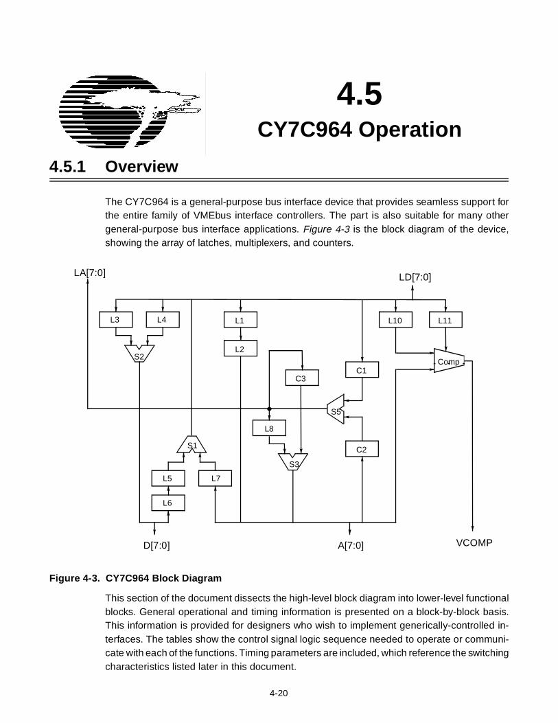
4-20
4.5CY7C964 Operation
4.5.1 Overview
The CY7C964 is a general-purpose bus interface device that provides seamless support forthe entire family of VMEbus interface controllers. The part is also suitable for many othergeneral-purpose bus interface applications. Figure 4-3 is the block diagram of the device,showing the array of latches, multiplexers, and counters.
Figure 4-3. CY7C964 Block Diagram
This section of the document dissects the high-level block diagram into lower-level functionalblocks. General operational and timing information is presented on a block-by-block basis.This information is provided for designers who wish to implement generically-controlled in-terfaces. The tables show the control signal logic sequence needed to operate or communi-cate with each of the functions. Timing parameters are included, which reference the switchingcharacteristics listed later in this document.
LA[7:0]
D[7:0] A[7:0] VCOMP
LD[7:0]
L3
S2
L4
S1
L5 L7
L6
L1
L2
L8
C3
C2
C1
L10 L11
Comp
S3
S5

CY7C964 Operation
4-21
The CY7C964 operation is controlled by the combination of external control signals andinternal state logic. Three internal asynchronous state bit control the operating mode of thedevice. These bits are referred to as BLT_STATE, BLT_INIT, and DUAL_PATH. TheBLT_STATE bit is set during block transfer operations. The block transfer initiation cycle gen-erates a rising edge on the BLT_INIT signal. The DUAL_PATH signal is the output of a trans-parent latch within the device that latches the state of LADO. These internal state bits mustbe in the proper state to use and communicate with the internal logic of the device. Thefunctional tables include references to these signals when their state is required for the op-eration. The designer must perform the appropriate cycle to the device to set or clear theselatches as needed prior to the desired functional cycle. The internal latch signals and all othercontrol signals that are not called out within the tables for a specific operation can be consid-ered don’t cares.
Table 4-5. Examples of References to Control Signals Within Functional Tables
Figure 4-4. CY7C964 Block Diagram: Address Counters and Address Multiplexers
Note 1: BLT_STATE=(/BLT* • /MWB*)+(BLT_STATE • (/BLT*+/MWB*+LAEN))
Note 2: BLT_INIT=(/BLT_STATE • /BLT* • /MWB*)+(BLT_INIT • /BLT* • /MWB*)
Note 3: DUAL_PATH=(LADO • BLT_INIT)+(DUAL_PATH • /BLT_INIT)
LA[7:0]
D[7:0] A[7:0] VCOMP
LD[7:0]
L3
S2
L4
S1
L5 L7
L6
L1
L2
L8
C3
C2
C1
L10 L11
Comp
S3
S5

CY7C964 Operation
4-22
4.5.2 Master Block Transfer Local Address Counter (C1)
Master Block Transfer Local Address Counter supplies the local address to LA[7:0] duringmaster block transfer operations. This 8-bit synchronous counter is cascadable using theLCIN*/LCOUT* daisy-chain. The counter powers up in an uninitialized state and must beinitialized for predictable operation. The counter loads from LD[7:0] when both MWB* andBLT* control signals are active (Low). To enable the counter onto LA[7:0], an internal asyn-chronous latch (BLT_STATE) must be set and Local Address Multiplexer S5 must selectcounter C1. A falling edge on MWB* or BLT* increments C1. FC1 controls S5. If it is High, asshown in Table 4-7, C1 is selected. The internal latch and S5 multiplexer must also be in theproper state to increment the counter. For further information on the S5 Local Address Mul-tiplexer, see section 4.5.3.
Table 4-6. Master Block Transfer Local Address Counter Operation
Logic Functional Description Operational Description Required Condition Parameter
C1 Load counter LD[7:0] valid to falling edge of MWB*
BLT*=0, LAEN=0 Set-up t48
Hold t49
LD[7:0] valid to falling edge of BLT*
MWB*=0, LAEN=0 Set-up t50
Hold t51
Increment counter MWB* falling edge to LA[7:0] valid
LAEN=1, FC1=1, BLT_STATE=1[1]
Prop t54
BLT* falling edge to LA[7:0] valid LAEN=1, FC1=1, BLT_STATE=1[1]
Prop t54
LCIN* valid to MWB* falling edge
LAEN=1, FC1=1, BLT_STATE=1[1]
Set-up t52
Hold t53
LCIN* valid to BLT* falling edge LAEN=1, FC1=1, BLT_STATE=1[1]
Set-up t52
Hold t53
Counter carry out at ter-minal count
MWB falling edge to LCOUT* valid
LAEN=1, FC1=1, BLT_STATE=1[1]
Prop t55
BLT* falling edge to LCOUT* valid
LAEN=1, FC1=1, BLT_STATE=1[1]
Prop t55
LCIN* valid to LCOUT* valid LAEN=1, FC1=1, BLT_STATE=1[1]
Prop t56
Minimum pulse widths BLT* LAEN=1, FC1=1, BLT_STATE=1[1]
t57
MWB* t57
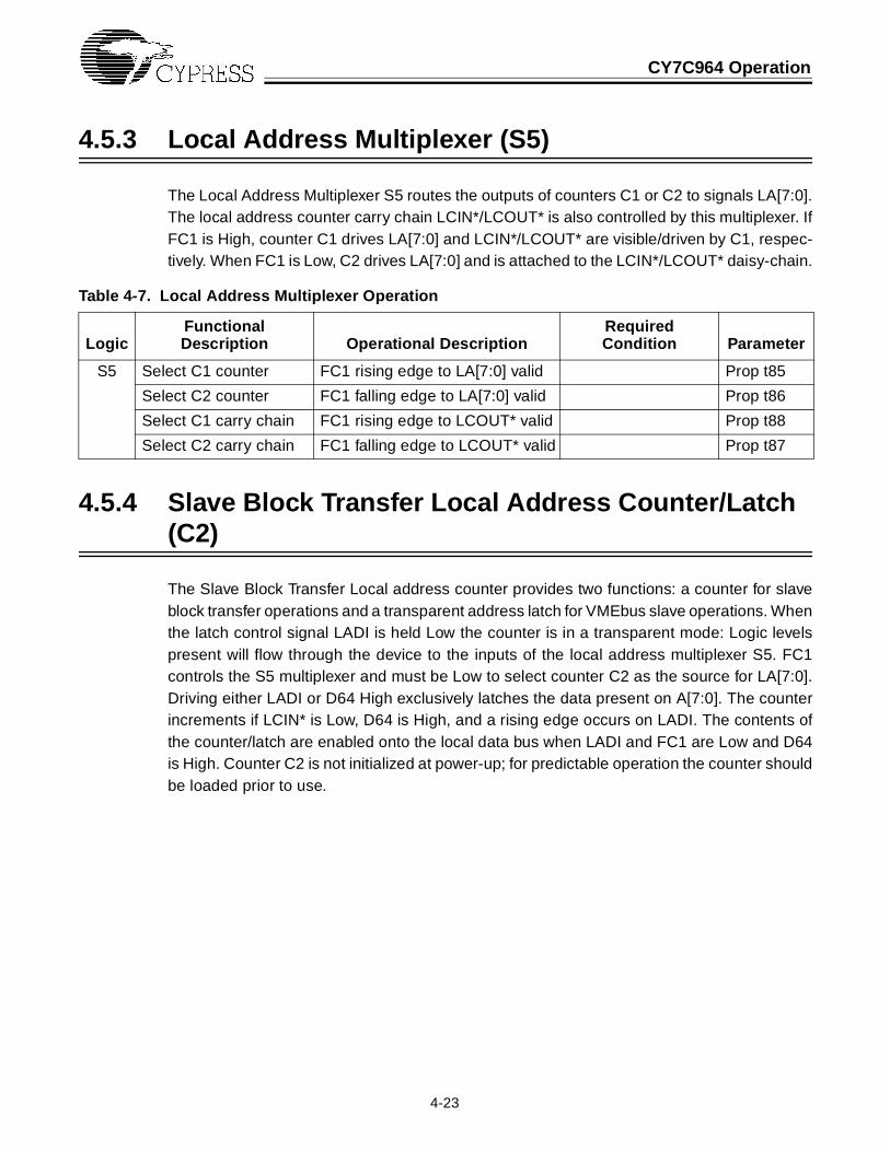
CY7C964 Operation
4-23
4.5.3 Local Address Multiplexer (S5)
The Local Address Multiplexer S5 routes the outputs of counters C1 or C2 to signals LA[7:0].The local address counter carry chain LCIN*/LCOUT* is also controlled by this multiplexer. IfFC1 is High, counter C1 drives LA[7:0] and LCIN*/LCOUT* are visible/driven by C1, respec-tively. When FC1 is Low, C2 drives LA[7:0] and is attached to the LCIN*/LCOUT* daisy-chain.
4.5.4 Slave Block Transfer Local Address Counter/Latch (C2)
The Slave Block Transfer Local address counter provides two functions: a counter for slaveblock transfer operations and a transparent address latch for VMEbus slave operations. Whenthe latch control signal LADI is held Low the counter is in a transparent mode: Logic levelspresent will flow through the device to the inputs of the local address multiplexer S5. FC1controls the S5 multiplexer and must be Low to select counter C2 as the source for LA[7:0].Driving either LADI or D64 High exclusively latches the data present on A[7:0]. The counterincrements if LCIN* is Low, D64 is High, and a rising edge occurs on LADI. The contents ofthe counter/latch are enabled onto the local data bus when LADI and FC1 are Low and D64is High. Counter C2 is not initialized at power-up; for predictable operation the counter shouldbe loaded prior to use.
Table 4-7. Local Address Multiplexer Operation
LogicFunctionalDescription Operational Description
Required Condition Parameter
S5 Select C1 counter FC1 rising edge to LA[7:0] valid Prop t85
Select C2 counter FC1 falling edge to LA[7:0] valid Prop t86
Select C1 carry chain FC1 rising edge to LCOUT* valid Prop t88
Select C2 carry chain FC1 falling edge to LCOUT* valid Prop t87

CY7C964 Operation
4-24
4.5.5 Master Block Transfer VMEbus Address Counter (C3)
The VMEbus Master Block Transfer Address stores and increments the VMEbus addressduring master block transfer operations. The counter loads from LA[7:0] on the rising edgeof MWB* provided that the internal asynchronous latch BLT_STATE is set. The contents ofthe counter are enabled onto the A[7:0] pins if the internal asynchronous latch bits BLT_STATEand multiplexer S3 are in the appropriate state. Depending on the state of DUAL_PATH, eitherthe rising or the falling edge of LADO increments C3. Counter C3 uses the VCIN*/VCOUT*counter daisy-chain. This counter is uninitialized at power-up and should be initialized priorto use for predictable operation.
Table 4-8. Slave Block Transfer Local Address Counter/Latch Operation
Logic Functional Description Operational Description Required Condition Parameter
C1 Load counter A[7:0] valid to D64 rising edge LADI=0 Set-up t58
Hold t59
A[7:0] valid to LADI rising edge D64=0 Set-up t60
Hold t61
Increment counter LADI rising edge to LA[7:0] D64=1, FC1=0 Prop t64
LCIN* active to LADI rising edge D64=1 Set-up t62
Hold t63
Counter carry out at terminal count
LADI rising edge to LCOUT* D64=1, FC1=0 Prop t65
Minimum pulse width LADI t66

CY7C964 Operation
4-25
4.5.6 VMEbus Address Latch (L8) and Multiplexer (S3)
The VMEbus Address Latch and Multiplexer selects the source for the VMEbus addresssignals A[7:0]. The information supplied to A[7:0] originates at one of three sources: the D64block transfer data pipeline latch L2, the VMEbus master block transfer counter C3, or theVMEbus address latch L8. Table 4-10 shows how to latch information into the VMEbus addresslatch L8 and control the selection of the source for signals A[7:0]. Latch L8 is uninitialized atpower-up and for predictable operation should be loaded prior to use.
Table 4-9. Master Block Transfer VMEbus Address Counter Operation
Logic Functional Description Operational Description Required Condition Parameter
C3 Load counter LA[7:0] valid to rising edge of MWB*
BLT_STATE=1[1]
BLT_INIT=1Set-up t67
Hold t68
Increment counter LADO falling edge to A[7:0] BLT_STATE=1[1]
DUAL_PATH=1[3]
BLT_INIT=0
Prop t69
LADO rising edge to A[7:0] BLT_STATE=1[1]
DUAL_PATH=0BLT_INIT=0
Prop t70
VCIN* valid to LADO rising/fall-ing edge
Set-up t134
Hold t135
Counter carry out LADO falling edge to VCOUT* valid
BLT_STATE=1[1]
DUAL_PATH=1[3]
BLT_INIT=0
Prop t71
LADO rising edge to VCOUT* valid
BLT_STATE=1[1]
DUAL_PATH=0BLT_INIT=0
Prop t72
Minimum pulse width LADO (High) t73
LADO (Low) t73
Table 4-10. VMEbus Address Latch and Multiplexer Operation
LogicFunctional Description Operational Description Required Condition Parameter
S3 Select L8 D64 falling edge to A[7:0] valid BLT_STATE=1[1] Prop t83
S3 Select L8 ABEN* falling edge to A[7:0] valid BLT_STATE=1[1] Prop t84
S3 Select L8 D64 falling edge to A[7:0] valid BLT_STATE=0 Prop t81
L8 Load L8 LA[7:0] valid to LADO rising edge Set-up t40
L8 Load L8 LA[7:0] valid to LADO rising edge Hold t41

CY7C964 Operation
4-26
4.5.7 VMEbus Address Comparator
The VMEbus Address Comparator is made up of three logic elements: an address maskregister, address compare register, and a high-performance, 8-bit, equality comparator. Thecompare and mask registers control the compare logic. The mask register contains an 8-bitvalue that enables or disables bits of the comparator. The compare register contains an 8-bitpattern. The enabled bits of the compare register are matched against the value on A[7:0]. Ifa match is detected (all active bits equal), the VCOMP* output pin is driven Low. Neither thecompare register nor the mask register are preset at power-up and must be initialized forpredictable operation. The act of writing the compare register clears the mask register. Thisprevents any inadvertent address compares during the configuration process. See Chapter4.3 for further information on the VMEbus address comparator.
Figure 4-5. CY7C964 Block Diagram: VMEbus Address Comparator
LA[7:0]
D[7:0] A[7:0] VCOMP
LD[7:0]
L3
S2
L4
S1
L5 L7
L6
L1
L2
L8
C3
C2
C1
L10 L11
Comp
S3
S5

CY7C964 Operation
4-27
Table 4-11. VMEbus Address Comparator Operation
4.5.8 VMEbus D64 Block Transfer Data Pipeline and Multiplexer
Latches L1 and L2 form a two-stage high-performance data pipeline for D64 block transferoperations. These latches load from the local signals LD[7:0], but drive VMEbus addresssignals A[7:0]. Latches L3 and L4 load from the local data signals LD[7:0] and in combinationwith multiplexer S2 drive D[7:0]. On the first cycle of a D64 block transfer, data on LD[7:0] iswritten to latch L1. During the second local data fetch of a D64 block transfer operation(D64=1), data from LD[7:0] is written to latch L3 and the data within latch L1 moves to L2.Two fetches must be performed to form the 64-bit block transfer data word. During non-D64modes of operation (D64=0), data from LD[7:0] is written to latch L4. This is the normal datapath from LD[7:0] to D[7:0] for all non-D64 operation. Because all the latches are implementedon transparent latches, L2 may be loaded from LD[7:0] when L1 is transparent (LEDO=0).None of the latches are initialized at power-up. Therefore, for predictable operation, theselatches should be written prior to their use.
Logic Functional Description Operational Description Required Condition Parameter
L10 Select compare register LDS, MWB* valid to STROBE falling edge
LDS=1, MWB*=1 Set-up t43
Hold t44
Load compare register LD[7:0] valid to STROBE rising edge
Set-up t46
Hold t47
L11 Select mask register LDS, MWB* valid to STROBE falling edge
LDS=0, MWB*=1 Set-up t43
Hold t44
Load mask register LD[7:0] valid to STROBE rising edge
Set-up t46
Hold t47
Compare out A[7:0] valid to VCOMP* valid Prop t23
A[7:0] valid to VCOMP* invalid
Prop t24
Minimum pulse width STROBE minimum pulse width t47

CY7C964 Operation
4-28
Figure 4-6. CY7C964 Block Diagram: D64 Block Tran sfer Data Pipe line and Multiplexer
Table 4-12. VMEbus D64 Block Tran sfer Data Pipeline and Multipl exer Operation
Logic Functional Description Operational Description Required Condition Parameter
L1 Load register LD[7:0] valid to LEDO rising edge Set-up t25
Hold t26
L2 Load register LD[7:0] valid to DENO*falling edge
LEDO=0 Set-up t28
Hold t29
Drive A[7:0] D64 rising edge to A[7:0] valid BLT_STATE=1 Prop t82
L3 Load register LD[7:0] valid to DENO*rising edge
Set-up t25
Hold t26
L4 Load register LD[7:0] valid to LEDO rising edge Set-up t131
Hold t132
S2 Multiplexer selects L3 drive D[7:0]
D64 rising edge to D[7:0] valid Prop t78
Multiplexer selects L4 drive D[7:0]
D64 falling edge to D[7:0] valid Prop t79
Minimum pulse width DENO* t30
LEDO t27
LA[7:0]
D[7:0] A[7:0] VCOMP
LD[7:0]
L3
S2
L4
S1
L5 L7
L6
L1
L2
L8
C3
C2
C1
L10 L11
Comp
S3
S5
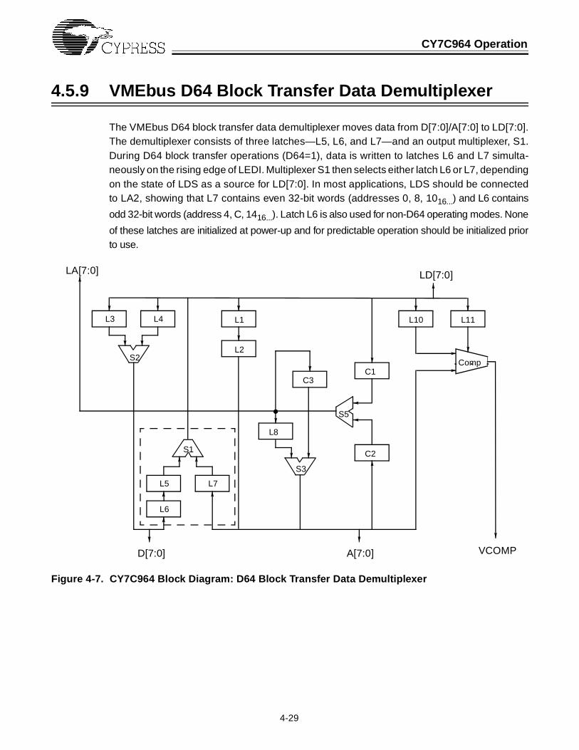
CY7C964 Operation
4-29
4.5.9 VMEbus D64 Block Transfer Data Demultiplexer
The VMEbus D64 block transfer data demultiplexer moves data from D[7:0]/A[7:0] to LD[7:0].The demultiplexer consists of three latches—L5, L6, and L7—and an output multiplexer, S1.During D64 block transfer operations (D64=1), data is written to latches L6 and L7 simulta-neously on the rising edge of LEDI. Multiplexer S1 then selects either latch L6 or L7, dependingon the state of LDS as a source for LD[7:0]. In most applications, LDS should be connectedto LA2, showing that L7 contains even 32-bit words (addresses 0, 8, 1016...) and L6 contains
odd 32-bit words (address 4, C, 1416...). Latch L6 is also used for non-D64 operating modes. None
of these latches are initialized at power-up and for predictable operation should be initialized priorto use.
Figure 4-7. CY7C964 Block Diagram: D64 Block Tran sfer Data Demultiplexer
LA[7:0]
D[7:0] A[7:0] VCOMP
LD[7:0]
L3
S2
L4
S1
L5 L7
L6
L1
L2
L8
C3
C2
C1
L10 L11
Comp
S3
S5

CY7C964 Operation
4-30
Table 4-13. VMEbus D64 Block Tran sfer Data Pipeline and Demultiplexer Operation
Logic Functional Description Operational Description Required Condition Parameter
L5 Load register D[7:0] valid to DENIN* falling edge
DENIN1*=0, LEDI=0 Set-up t31
Hold t32
Load register D[7:0] valid to DENIN1* falling edge
DENIN*=0, LEDI=0 Set-up t34
Hold t35
L6 Load register D[7:0] valid to LEDI rising edge LEDO=0 Set-up t37
Hold t38
L7 Load register A[7:0] valid to LEDI rising edge LEDO=0 Set-up t37
Hold t38
S1 Select L5 LDS rising edge to LD[7:0] valid D64=1 Prop t74
D64 rising edge to LD[7:0] valid
LDS=1 Prop t76
Select L7 LDS falling edge to LD[7:0] valid D64=1 Prop t75
Select L6 D64 falling edge to LD[7:0] valid
Prop t77
Minimum pulse width DENIN* t33
DENIN1* t36
LEDI t39
4-31
4.6 CY7C964 Alternate BLT Initiation Operation for
VIC068A and VIC64Another method of loading the VMEbus block transfer address counters exists within theCY7C964. This method has been placed within its own section of the document because itis not completely compatible with the VIC block transfer initiation cycle.
The CY7C964 determines the source for loading the VMEbus master block transfer counterC3 by monitoring the arrival sequence of the MWB* and BLT* signals. For typical block transferinitiation cycles, the assertion of MWB* occurs prior to the assertion of the BLT*. The VMEbusmaster block transfer counter C3 loads from the local address pins, LA[7:0], as describedwithin section 4.5.5.
Reversing the arrival order of these two signals changes the operation of the device. This isdone at system design time by swapping the BLT* and MWB* inputs to the CY7C964. Forproper operation, these signals must continue to operate in the same manner as they do onthe VIC, even though they are no longer connected to the associated input pins on theCY7C964 which have the same name. Swapping these signals on the device changes theway that the VMEbus master block transfer counter C3 is loaded. In this mode it loads fromthe local data bus via latch L9. All other functions within the device operate in the same manneras described in Chapter 4.5.
Loading C3 is accomplished with a local cycle similar to the cycles needed to load the maskand compare registers. This cycle operates as follows: LDS is driven High, (most likely thissignal is connected to LA2), the MWB* input pin of the CY7C964 is driven Low, (this pin isactually connected to the open collector BLT* output of the VIC), and STROBE is asserted.The local data bus should be driven to the appropriate value for the address to load into theC3 counters. STROBE is deasserted and the data is latched into L9 within the CY7C964.The local address decode signal used to assert MWB* on the CY7C964, (BLT* on the VIC),must be a three-state or an open-collector output. This signal must not be driven High or theVIC will be unable to perform block transfers.
A normal master block transfer initiation cycle is then performed, with one minor exception.The lower 8 bits of address LA[7:0] which are controlled by the VIC, must contain the desiredlower address. This is needed because the VIC operates in the typical block transfer initiationmode. The upper address LA[31:8] will be ignored by the CY7C964s during the initiation cycle.
This mode of operation allows the VMEbus master block transfer address counters to beloaded independent of the VMEbus address. This has advantages in some designs, but C3cannot be used to source single cycle transfer addresses. This limitation should be consideredwhile performing the design analysis to use this mode.

CY7C964 Alternate BLT Initiation Operation for VIC068A and VIC64
4-32
Table 4-14. Master Block Transfer Local Address Counter Operation
Figure 4-8. CY7C964 Alternate BLT Operation Block Diagram
Logic Functional Description Operational Description Required Condition Parameter
L9 Select register LDS, MWB* valid to STROBE falling edge
LDS=1, MWB*=0 Set-up t43
Hold t44
Load register LD[7:0] valid to STROBE rising edge
Set-up t45
Hold t46
Minimum pulse width STROBE t46
LA[7:0]
D[7:0] A[7:0] VCOMP
LD[7:0]
L3
S2
L4
S1
L5 L7
L6
L1
L2
L8
C3
C2
C1
L10 L11
Comp
S3
L9
S5

4-33
4.7 DC Performance
SpecificationsTable 4-15. VMEbus Signals (A[7:0], D[7:0])
Parameter Description Test Conditions Comm. Industrial Military Units
VIH MinimumHigh-LevelInput Voltage
2.0 2.0 2.0 V
VIL MaximumLow-LevelInput Voltage
0.8 0.8 0.8 V
VOH MinimumHigh-LevelOutput Voltage
VCC = Min.,IOH = –3 mA
2.4 2.4 2.4 V
VOL MaximumLow-LevelOutput Voltage
VCC = Min.,IOL = 48 mA
0.6 0.6 0.6 V
IL MaximumInput LeakageCurrent
VCC = Max.,VIN = 0.6–2.4
±5 ±5 ±5 µA
VIK Input ClampVoltage
VCC = Min. IIN= –18 mA –1.2 –1.2 –1.2 V
VIK Input ClampVoltage
VCC = Min. IIN = 18 mA VCC+1.2 VCC+1.2 VCC+1.2 V
IOZ MaximumOutput LeakageCurrent
VCC = Max.GND < VOUT < VCCAll Outputs Disabled
±10 ±10 ±10 µA

DC Performance Specifications
4-34
Table 4-16. Non-VMEbus Signals
Table 4-17. Operating Current
Parameter Description Test Conditions Comm. Industrial Military Units
VIH MinimumHigh-LevelInput Voltage
2.0 2.0 2.0 V
VIL MaximumLow-LevelInput Voltage
0.8 0.8 0.8 V
VOH MinimumHigh-LevelOutput Voltage
VCC = Min.,IOH = –8 mA
2.4 2.4 2.4 V
VOL MaximumLow-LevelOutput Voltage
VCC = Min.,IOL = 8 mA
0.6 0.6 0.6 V
IL MaximumInput LeakageCurrent
VCC = Max.,VIN = 0.00 – VCC
±5 ±5 ±5 µA
VIK Input ClampVoltage
VCC = Min. IIN= –18 mA –1.2 –1.2 –1.2 V
VIK Input ClampVoltage
VCC = Min. IIN = 18 mA VCC+1.2 VCC+1.2 VCC+1.2 V
IOZ MaximumOutput LeakageCurrent
VCC = Max.GND < VOUT < VCCAll Outputs Disabled
±5 ±5 ±5 µA
ICC VCC Maximum Operating Supply Current
VCC = Max.,All Outputs Disabled
25 25 25 mA
Parameters Description Test Conditions Max. Units
IDD Maximum Operating Current
No external DC load 50 mA

4-35
4.8 AC Performance
Specifications
Parameter DescriptionMin. All
Grades [1]Max.
(Com’l)Max. (Ind)
Max. (Mil) Unit Comment
t1 LA[7:0] to A[7:0] propagation delay[2] 15 16 18 ns
t2 LD[7:0] to D[7:0] propagation delay 16 17 19 ns
t3 A[7:0] to LA[7:0] propagation delay 17 18 20 ns
t4 D[7:0] to LD[7:0] propagation delay[2] 19 20 22 ns
t5 LD[7:0] to A[7:0] propagation delay[2] 19 20 22 ns D64=1
t6 A[7:0] to LD[7:0] propagation delay[2] 19 20 22 ns D64=1
t7 ABEN* active to A[7:0] output enable delay[2]
11 11 12 ns
t8 DENO* active to D[7:0] output enable de-lay[2]
14 15 16 ns
t9 ABEN* active to D[7:0] output enable delay
14 15 17 ns D64=1
t10 D64 active to D[7:0] output enable delay[2] 13 14 15 ns ABEN*=0
t11 LAEN active to LA[7:0] output enable delay[2]
10 11 12 ns
t12 DENIN* active to LD[7:0] output enable delay
15 16 18 ns
t13 DENIN1* active to LD[7:0] output enable delay[2]
18 19 21 ns D64=1
t14 D64 active to LD[7:0] output enable delay[2]
18 19 21 ns DENIN1*=0
t15 ABEN* inactive to A[7:0] High-Z output disable delay[2]
8 10 12 ns
t16 DENO* inactive to D[7:0] High-Z output disable delay[2]
12 14 15 ns
t17 ABEN* inactive to D[7:0] High-Z output disable delay[2]
12 14 15 ns D64=1
t18 D64 inactive to D[7:0] High-Z output disable delay[2]
14 15 16 ns ABEN*=0
t19 LAEN inactive to LA[7:0] High-Z output disable delay[2]
13 14 15 ns
t20 DENIN* inactive to LD[7:0] High-Z output disable delay[2]
14 16 18 ns
t21 DENIN1* inactive to LD[7:0] High-Z output disable delay[2]
14 16 18 ns D64=1
t22 D64 inactive to LD[7:0] High-Z output disable delay[2]
19 21 24 ns DENIN1*=0

AC Performance Specifications
4-36
t23 A[7:0] to VCOMP* High-to-Low propagation delay
18 19 21 ns
t24 A[7:0] to VCOMP* Low-to-High propagation delay
16 17 19 ns
t25 LD[7:0] set-up time to LEDO rising edge 7 ns
t26 LD[7:0] hold time after LEDO rising edge 0 ns
t27 LEDO minimum pulse width 7 ns
t28 LD[7:0] set-up time to DENO* falling edge 0 ns LEDO=0
t29 LD[7:0] hold time after DENO* falling edge 7 ns LEDO=0
t30 DENO* minimum pulse width 10 ns
t31 D[7:0] set-up time to DENIN* falling edge 5 ns DENIN1*=0, LEDI=0
t32 D[7:0] hold time after DENIN* falling edge 5 ns DENIN1*=0, LEDI=0
t33 DENIN* minimum pulse width 10 ns
t34 D[7:0] set-up time to DENIN1* falling edge 5 ns
t35 D[7:0] hold time after DENIN1* falling edge
5 ns
t36 DENIN1* minimum pulse width 10 ns
t37 D[7:0], A[7:0] set-up time to LEDI rising edge
7 ns
t38 D[7:0], A[7:0] hold time after LEDI rising edge
0 ns
t39 LEDI minimum pulse width 10 ns
t40 LA[7:0] set-up time to LADO rising edge 5 ns
t41 LA[7:0] hold time after LADO rising edge 5 ns
t42 LADO minimum pulse width 10 ns
t43 MWB*, LDS set-up time to STROBEfalling edge
0 ns
t44 MWB*, LDS hold time after STROBE falling edge
5 ns
t45 LD[7:0] set-up time to STROBE rising edge
5 ns
t46 LD[7:0] hold time after STROBE rising edge
5 ns
t47 STROBE minimum pulse width 10 ns
t48 Local master block transfer address counter C1 LD[7:0] set-up time before MWB* falling edge
0 ns BLT*, LAEN=0
t49 Local master block transfer address counter C1 LD[7:0] hold time after MWB* falling edge
5 ns BLT*, LAEN=0
t50 Master block transfer local address counter C1 LD[7:0] set-up time to BLT* fall-ing edge
0 ns MWB*, LAEN=0
t51 Master block transfer local address counter C1 LD[7:0] hold time after BLT* falling edge
5 ns MWB*, LAEN=0
Parameter DescriptionMin. All
Grades [1]Max.
(Com’l)Max. (Ind)
Max. (Mil) Unit Comment

AC Performance Specifications
4-37
t52 LCIN* set-up time to MWB* falling edge 5 ns BLT_STATE, LAEN, FC1=1
t53 LCIN hold time after MWB* or BLT* falling edge
0 ns BLT_STATE, LAEN, FC1=1
t54 MWB*, BLT* falling edge to LA[7:0] propagation delay
21 22 25 ns BLT_STATE, LAEN, FC1=1
t55 MWB*, BLT* falling edge to LCOUT* prop-agation delay
24 25 28 ns BLT_STATE, LAEN, FC1=1
t56 LCIN* to LCOUT* propagation delay[2] 17 18 20 ns BLT_STATE, LAEN, FC1=1
t57 BLT*, MWB* minimum pulse width 10 ns
t58 Slave block transfer local address counter C2, A[7:0] set-up time to D64 rising edge
5 ns LADI=0
t59 Slave block transfer local address counter C2, A[7:0] hold time after D64 rising edge
5 ns LADI=0
t60 Slave block transfer local address counter C2, A[7:0] set-up time to LADI rising edge
5 ns D64=0
t61 Slave block transfer local address counter C2, A[7:0] hold time after LADI rising edge
5 ns D64=0
t62 LCIN* set-up time to LADI rising edge 8 ns D64=1
t63 LCIN* hold time after LADI rising edge 0 ns D64=1
t64 LADI rising edge to LA[7:0] validpropagation delay
15 16 18 ns D64=1, FC1=0
t65 LADI rising edge to LCOUT* valid propagation delay
20 21 24 ns D64=1, FC1=0
t66 LADI minimum pulse width 10 ns
t67 Master block transfer VMEbus address counter LA[7:0] set-up time to MWB* rising edge
5 ns BLT_STATE=1, BLT_INIT=1
t68 Master block transfer VMEbus address counter LA[7:0] hold time after MWB* rising edge
5 ns BLT_STATE=1, BLT_INIT=1
t69 LADO falling edge to A[7:0] valid propagation delay
23 24 27 ns BLT_STATE, DUAL_PATH=1, BLT_INIT=0
t70 LADO rising edge to A[7:0] valid propagation delay[2]
24 25 28 ns BLT_STATE=1, DUAL_PATH=0, BLT_INIT=0
t71 LADO falling edge to VCOUT* valid propagation delay
26 27 30 ns BLT_STATE, DUAL_PATH=1, BLT_INIT=0
t72 LADO rising edge to VCOUT* valid propagation delay[2]
30 33 36 ns BLT_STATE, DUAL_PATH=0, BLT_INIT=0
t73 LADO minimum High or Low pulse width 10 ns
t74 LDS rising edge to LD[7:0] valid propagation delay[2]
20 21 24 ns D64=1
t75 LDS falling edge to LD[7:0] valid propagation delay
20 21 24 ns D64=1
Parameter DescriptionMin. All
Grades [1]Max.
(Com’l)Max. (Ind)
Max. (Mil) Unit Comment

AC Performance Specifications
4-38
t76 D64 rising edge to LD[7:0] valid propagation delay[2]
21 22 24 ns
t77 D64 falling edge to LD[7:0] valid propagation delay
21 22 24 ns
t78 D64 rising edge to D[7:0] valid propagation delay[2]
16 16 18 ns
t79 D64 falling edge to D[7:0] valid propagation delay[2]
19 19 21 ns
t80 D64 rising edge to A[7:0] valid propagation delay[2]
15 16 18 ns BLT_STATE=0
t81 D64 falling edge to A[7:0] valid propagation delay[2]
16 17 19 ns BLT_STATE=0
t82 D64 rising edge to A[7:0] valid propagation delay[2]
19 19 22 ns BLT_STATE=1
t83 D64 falling edge to A[7:0] valid propagation delay
20 21 23 ns BLT_STATE=1
t84 ABEN* falling edge to A[7:0] valid propagation delay[2]
11 11 12 ns BLT_STATE=1
t85 FC1 rising edge to LA[7:0] valid propagation delay[2]
14 15 17 ns
t86 FC1 falling edge to LA[7:0] valid propagation delay
17 18 20 ns
t87 FC1 falling edge to LCOUT* valid propagation delay[2]
17 18 20 ns
t88 FC1 rising edge to LCOUT* valid propagation delay
17 18 20 ns
t89 LADO set-up time to MWB*, BLT* rising edge
0 ns BLT_STATE=1
t136 LADO hold time after MWB*, BLT* rising edge
7 ns BLT_STATE=1
t137 BLT* set-up time to MWB* falling edge 5 ns
t90 BLT* hold time after MWB* falling edge 5 ns
t131 LD[7:0] to DENO* falling edge set-up 5 ns
t132 LD[7:0] after DENO* falling edge 5 ns
t133 LCIN* hold time after BLT* falling edge 5 ns
Notes:
1. All minimum times guaranteed by design, not tested.
2. Guaranteed, not tested.
Parameter DescriptionMin. All
Grades [1]Max.
(Com’l)Max. (Ind)
Max. (Mil) Unit Comment

4-39
4.9 Pin Description
4.9.1 Pin Definitions
QFP Pin No.
PGAPin No. Signal Name Type Description
1 E1 GND Power Ground
2 L2 LD7 Three-state I/O Local data transceiver 7
3 K3 LDS Input Register select bit
4 L3 FC1 Input Function code 1 control signal
5 K4 STROBE Input Comparator register load control signal
6 L4 MWB* Input Module wants VMEbus control signal
7 K5 LCOUT* Output Local address counters carry out signal
8 L5 GND Power Ground
9 K6 VCOMP* Output VMEbus address comparator out signal
10 L6 VCOUT* Output VMEbus address counter carry out signal
11 K7 LADO Input Latch address out control signal
12 L7 LADI Input Latch address in control signal
13 K8 LEDI Input Latch enable data in control signal
14 L8 LEDO Input Latch enable data out control signal
15 K9 A7 Three-state I/O High drive address transceiver 7
16 A3 GND Power Ground
17 A2 VCC Power VCC
18 K11 D7 Three-state I/O High drive data transceiver 7
19 J10 A6 Three-state I/O High drive address transceiver 6
20 J11 D6 Three-state I/O High drive data transceiver 6
21 H10 A5 Three-state I/O High drive address transceiver 5
22 H11 D5 Three-state I/O High drive data transceiver 5
23 G10 A4 Three-state I/O High drive address transceiver 4
24 G11 D4 Three-state I/O High drive data transceiver 4
25 L9 GND Power Ground
26 F11 A3 Three-state I/O High drive address transceiver 3
27 E10 D3 Three-state I/O High drive data transceiver 3
28 E11 A2 Three-state I/O High drive address transceiver 2

Pin Description
4-40
29 D10 D2 Three-state I/O High drive data transceiver 2
30 D11 A1 Three-state I/O High drive address transceiver 1
31 C10 D1 Three-state I/O High drive data transceiver 1
32 K10 VCC Power VCC
33 B10 GND Power Ground
34 A10 A0 Three-state I/O High drive address transceiver 0
35 B9 D0 Three-state I/O High drive data transceiver 0
36 A9 ABEN* Input High drive address bus enable signal
37 B8 DENO* Input High drive data bus enable signal
38 A8 D64 Input D64 mode enable control signal
39 B7 BLT* Input Block transfer control signal
40 B2 VCC Power VCC
41 B6 VCIN* Input VMEbus address counter count enable signal
42 A6 LCIN* Input Local address counter count enable signal
43 B5 LAEN Input Local address enable control signal
44 A5 DENIN1* Input Data enable in 1 control signal
45 B4 DENIN* Input Data enable in control signal
46 A4 LA0 Three-state I/O Local address transceiver 0
47 B3 LD0 Three-state I/O Local data transceiver 0
48 F10 GND Power Ground
49 A7 VCC Power VCC
50 B1 LA1 Three-state I/O Local address transceiver 1
51 C2 LD1 Three-state I/O Local data transceiver 1
52 C1 LA2 Three-state I/O Local address transceiver 2
53 D2 LD2 Three-state I/O Local data transceiver 2
54 D1 LA3 Three-state I/O Local address transceiver 3
55 E2 LD3 Three-state I/O Local data transceiver 3
56 L10 GND Power Ground
57 F2 LA4 Three-state I/O Local address transceiver4
58 F1 LD4 Three-state I/O Local data transceiver 4
59 G2 LA5 Three-state I/O Local address transceiver 5
60 G1 LD5 Three-state I/O Local data transceiver 5
61 H2 LA6 Three-state I/O Local address transceiver 6
62 H1 LD6 Three-state I/O Local data transceiver 6
QFP Pin No.
PGAPin No. Signal Name Type Description
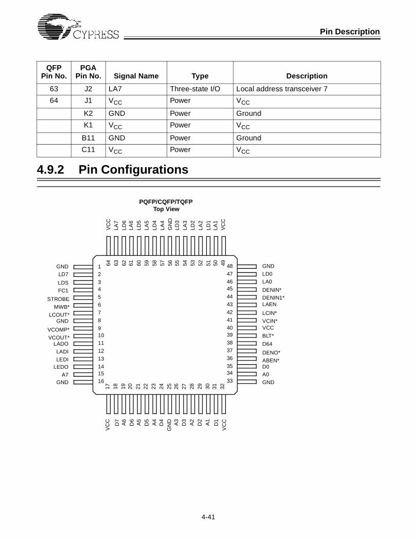
Pin Description
4-41
4.9.2 Pin Configurations
63 J2 LA7 Three-state I/O Local address transceiver 7
64 J1 VCC Power VCC
K2 GND Power Ground
K1 VCC Power VCC
B11 GND Power Ground
C11 VCC Power VCC
QFP Pin No.
PGAPin No. Signal Name Type Description
PQFP/CQFP/TQFPTop View
1GND2LD7
34
LDS
5FC1
6
7
8GND91011LADO12LADI13LEDI14
A7 15
GND
48 GND
47 LD046 LA045
44
43 LAEN
4241
40 VCC39
38 D6437
36
3534
D0
33A0
GND
17V
CC
64V
CC
18
A6
63LA
719
D6
62LD
620
A5
61LA
621
D5
60LD
522
A4
59LA
523
58LD
424
D4
57LA
425
GN
D56
GN
D26
A3
55LD
327
D3
54LA
328
A2
53LD
229
D2
52LA
230
A1
51LD
131
D1
50LA
132
49V
CC
DENIN1*DENIN*
LCIN*
VCIN*
BLT*
DENO*
ABEN*
STROBE
MWB*
LCOUT*
VCOUT*
16
LEDO
VC
C
VCOMP*
D7

Pin Description
4-42
11 10 9 8 7 6 5 4 3 2 1
A
B
C
D
E
F
J
K
L
G
H
GND
VCC
A2
A3
D4
D5
D6
D7
GND
D1
D2
D3
GND
A4
A5
A6
A0
VCC
GND
ABEN*
D0
A7
GND
D64
DENO*
LEDI
LEDO
VCC
BLT*
LCIN*
VCIN*
LADO
LADI
VCOMP*
VCOUT*
DENIN1*
LAEN
LCOUT*
GND
LA0
DENIN*
STROBE
MWB*
GND
LD0
LDS
FC1
VCC
VCC
LD1
LD2
LD3
LA4
LA5
LA6
LA7
GND
LD7
LA1
LA2
LA3
GND
LD4
LD5
LD6
VCC
VCC
A1
68-Pin Ceramic PGABottom View
Index MarkOn Top

4-43
4.10Package Diagrams
64-Pin Thin Quad Flat Pack A64

Package Diagrams
4-44
68-Pin Grid Array (Cavity Up) G68

Package Diagrams
4-45
64-Lead Plastic Thin Quad Flatpack N65
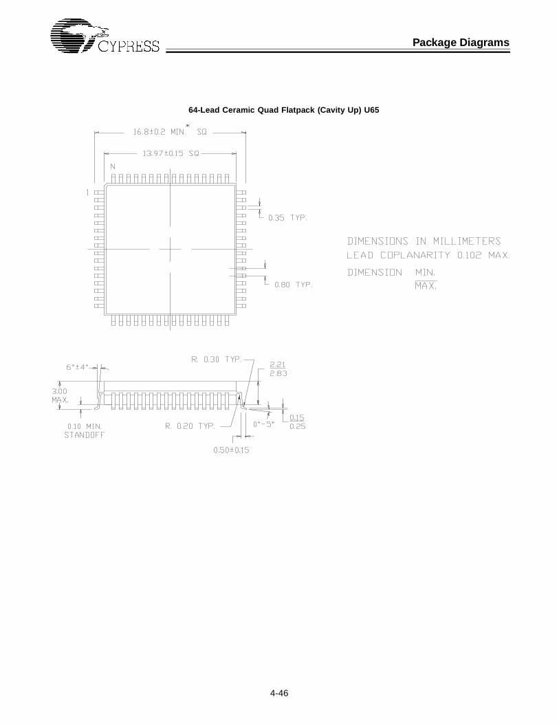
Package Diagrams
4-46
64-Lead Ceramic Quad Flatpack (Cavity Up) U65

Section 5
The VAC068A VMEbus Address Controller

5-1
5.1Introduction to the VAC068A
5.1.1 Features Summary
When used with the VIC068A (VMEbus Interface Controller), the VAC068A (VMEbus AddressController) forms a complete VMEbus master/slave interface solution. The VAC068A is in-tended for use solely with VIC068A. The following feature list is VAC068A specific but usesVIC068A implementations for items such as boundary crossing, dual-path, interprocessorcommunications facilities, and block transfers.
• Complete VMEbus and I/O DMA capability for 32-bit processors, including 42 program-mable registers for configuration and control of:
— slave address decode
— UARTs
— programmable I/O signals
— local I/O
— interrupt source
• Provides complete local memory map decoding. Separate segments on local interfaceavailable for:
— DRAM
— VME Subsystem Bus (VSB)
— Shared Resource
— Local I/O
— EPROM
• Provides complete VMEbus memory map decoding. Separate segments are available for:
— two VMEbus slave decodes
— interprocessor communication facilities
• Supports block transfers over 256-byte boundaries:
— address counters for VMEbus A[31:8] and local LA[31:8]
— supports dual-path feature of the VIC068A
— supports implementation of the VSB interface
— includes local DMA capability
• Dual UARTs on chip:
— double buffered on transmit, quad-buffered on receive
— programmable baud rate from 300 to 9600 baud

Introduction to the VAC068A
5-2
• Miscellaneous:
— supports unaligned transfers
— programmable DSACKi* for local I/O
— programmable timer and interrupts
— programmable I/O signals (dual function)
— buffer control signals for direct connection to ’543s
5.1.2 General Description
The VAC068A is a programmable address decode controller and VMEbus DMA extension forthe VIC068A. When used in conjunction with the VIC068A, the VAC068A maximizes perfor-mance of a master/slave VMEbus interface module. It also substantially reduces power con-sumption and board space when compared to discrete implementations. The VAC068A con-tains programmable registers that allow the user to easily define VMEbus address decoding.These are:
• A24 address space overlay register
• three programmable VMEbus boundary registers
• separate A16 address space with programmable D16 or D32 data size
The VAC068A reserves address space for local I/O resources, DRAM, and EPROM. Accessto these address spaces forces the proper chip select signal on the VAC068A. The chip selectoutputs are CS*, IOSEL5–0*, DRAMCS*, and EPROMCS*. DRAM address space is hardcoded to start at $0000 0000 to follow normal VMEbus address space conventions. Program-mable address options also exist for the purpose of asserting VSB select (VSBSEL*) andshared resources chip select (SHRCS*).
The VAC068A contains address counters and control logic to allow for block transfer over256-byte boundaries.
Additional features include 13 programmable input/output signals (PIO signals) that can beprogrammed for the following functions:
• 13 general-purpose I/O signals
• two serial I/O transmit and receive channels (A and B)
• three interrupt signals
• shared resource chip select
• I/O read and I/O write
• I/O selects 2–5 for slower 8-bit peripheral devices
Note: IOSEL0* and IOSEL1* have dedicated pins on the VAC068A.
The I/O selects have reserved address space and may use the local address bus or the IDbus.When the IDbus is used, programmable cycle end and DSACK control may be programmedin the corresponding DSACK control register.

Introduction to the VAC068A
5-3
Programmable DSACKi* control also exists for EPROM and shared resource selects. DSAC-Ki*s may also be disabled if the user wishes to provide this function. There is also a program-mable timer and interrupt mapping on either PIO7, PIO10, or PIO11 for the following inter-rupting functions:
• timer interrupt
• UART A and B interrupt
• mailbox interrupt
• PIO4, PIO7, PIO8, or PIO9
The VAC068A uses the VIC068A data direction (DDIR) and swapping signals (SWDEN*) fordirection control and unaligned transfers.
The VAC068A connects directly to the local address bus LA[31:8] and the VMEbus addressA[31:8] signals. It also connects to the local data bus through the IDbus ID[15:8]. VAC068Auses the IDbus to provide VMEbus data signal connection D[15:8], although external buffersand line drivers are required. The VIC068A directly drives the VMEbus data signals D[7:0],address signals A[7:1], and local address LA[7:1] and data signals D[7:0].
Both parts utilize Cypress’s patented output drivers and were designed with high-performancestandard cells using a 1-micron CMOS process. Thirteen ground and nine power pins areprovided.

5-4
5.2VAC068A Signal
Descriptions5.2.1 VMEbus Signals
A[31:8]
Drive: 64 mA (all) Type: Three-state I/O
These are the VMEbus address signals.
AS*
Type: Input
This is the VMEbus address strobe signal. It responds to both VIC068A- and VMEbus-gen-erated address strobes.
ID[15:8]
Drive: 16 mA Type: Three-state I/O
These are the isolated data bus signals. They are used to interface local data [15:8] to theVMEbus D[15:8] in conjunction with transparent latching bidirectional I/O buffers. They alsoare used to interface with local 8-bit I/O peripherals via the Device Location and DSACKi*Control registers.
5.2.2 CPU/Local Interface Signals
LD[31:16]
Drive: 16 mA Type: Three-state I/O
These are the local data bus signals. They are used to write or read the local data bus andfor writing and reading the on-chip control registers.
Note: The IDbus connects to LD[15:8] and VIC068A connects to LD[7:0].
VAC068A Signal Descriptions
5-5
LA[31:8]
Drive: 16 mA Type: Three-state I/O
These are the local address bus signals. They are used as inputs during a VMEbus mastercycle and to access on-chip control registers. They are used for output during local or slaveaccesses.
PAS*
Type: Input
This is the local-processor address strobe. It indicates to the VAC068A that a valid addressis present on the address bus. This signal is typically driven by either VIC068A or the localprocessor.
R/W*
Type: Input
This is the local read/write signal. When High, this signal indicates that the current cycle is aread. When Low, the current cycle is a write. This signal is typically driven by either theVIC068A or the local processor.
RESET*
Type: Input
This is the reset for the VAC068A. It is used alone or in conjunction with WORD* to reset theVAC068A internal registers. There are two reset types that may be implemented, and both ofthem are discussed in the reset section.
WORD*
Drive: 16 mA Type: Input/Three-state output
This signal is active under programmable control from the appropriate region attribute registerand controls the length of the data field. When it is asserted, the data path is 16 bits wide.When deasserted, a 32-bit data path is set. It is also used as an input in conjunction withRESET* to set VAC068A registers. It is typically connected to the VIC068A as an output.
ASIZ1, ASIZ0
Drive: 16 mA Type: Three-state output
These are the address size signals. They are used to specify the address size of an access.They are active under programmable control from the appropriate region attribute register.These signals are typically driven to VIC068A along with WORD* to determine address anddata path size.

VAC068A Signal Descriptions
5-6
ASIZ0 ASIZ1 Addressing Mode
0 0 User-defined0 1 A321 0 A16 1 1 A24
DSACK1/0*
Drive: 16 mA Type: Three-state I/O (rescinding)
These are the data sizing acknowledge signals. They are generated for any of the VAC068Adevice select outputs except CS* and VSBSEL* accesses. DSACK0* or DSACK1* can beselectively disabled or enabled in the DSACK1* Control register.
FC2/0
Type: Inputs
These are the function code signals. They are used by the VAC068A to determine the localaccess type and are typically driven by the local processor or the VIC068A as shown in thefollowing tables:
(Per 680X0 User’s Guide)
FC2 FC1 FC0 Cycle
0 0 1 User Data Space 0 1 0 User Program Space 1 0 1 Supervisor Data Space 1 1 0 Supervisor Program Space 1 1 1 CPU Space
(Per section 1.2.2 of this Handbook)
FC2 FC1 Cycle
0 0 Slave Block Transfer 0 1 Local DMA1 0 Slave Access 1 1 DRAM Refresh
MWB*
Drive: 16 mA Type: Output
This is the module-wants-bus signal. It is asserted under programmable control of the appro-priate region attribute register and indicates that a VMEbus access is occurring. This signalis typically connected to the VIC068A.
VAC068A Signal Descriptions
5-7
FCIACK*
Drive: 16 mA Type: Output
This is the local interrupt acknowledge signal. It indicates that the current cycle is an interruptacknowledge cycle. This signal is typically connected to the VIC068A. It is asserted duringlocal VAC068A interrupt cycles, or when HIACKEN is enabled in the PIO Direction registeror when IOSEL5* address space is accessed when enabled in the PIO Function register.
DRAMCS*
Drive: 16 mA Type: Output
This is the DRAM chip select signal. It is asserted when the local address maps into region0 as defined by the DRAM Upper Limit Address register. It is also asserted when redirectionis enabled in the VAC068A Decode Control register.
EPROMCS*
Drive: 16 mA Type: Output
This is the EPROM chip select signal. It is asserted after a global reset, during a local accessto EPROM address space, and during redirection of SLSEL1* on the local bus via theVAC068A Decode Control register.
FPUCS*
Drive: 16 mA Type: Output
This is the floating-point-unit chip select signal. It is asserted when a floating-point coproces-sor access is occurring. This is decoded from the processor function codes or under program-mable control in the PIO Function register to be asserted in the IOSEL4* address range.
VSBSEL*
Drive: 16 mA Type: Output
This is the VSB (VME Subsystem Bus) select signal. It is used to identify accesses to adaughterboard or VSB. It is asserted when enabled from the appropriate region attributeregister.
REFGT*
Drive: 16 mA Type: Output
This is the refresh grant signal. It is asserted during a DRAM refresh cycle and is typicallydecoded from the VIC068A function codes (FC1 and FC2).
VAC068A Signal Descriptions
5-8
LBR*
Type: Input
This is the VIC068A local bus request signal. It is used to signal the VAC068A when theVIC068A requests the local bus. It is typically connected to the VIC068A LBR* signal.
CS*
Drive: 16 mA Type: Output
This is the VIC068A chip select signal. It is asserted when the fixed address of the VIC068Ais present on the local address bus. This signal is typically connected to the VIC068A chipselect signal (CS*).
BLT*
Type: Input
This is the block transfer signal. It is used to determine when a block transfer is in progressand to increment internal address counters during a boundary crossing. This signal is typicallyconnected to the VIC068A.
CACHINH*
Drive: 16 mA Type: Open Collector Output
This is the cache inhibit signal. It is asserted when enabled in either the Region Attributeregisters or in the A24 Space Base Address register. It is also asserted on access to theDRAM Mailbox and VMEbus A16 address space (Region 6). It may be connected to the CDISsignal on 680X0-type processors.
LDMACK*
Drive: 16 mA Type: Output
This is the local DMA activity signal. It is asserted when there is DMA activity mapped into aparticular region. It is typically decoded from the VIC068A function codes (FC1 and FC2).
CPUCLK
Type: Input
This is the CPU clock signal. It is typically connected to the system CPU clock. Maximumfrequency is 50 MHz.

VAC068A Signal Descriptions
5-9
SLSEL0*
Drive: 16 mA Type: Output
This is the slave select 0 signal. It is asserted when enabled by a comparison of its baseaddress register and the address on the VMEbus. It indicates to the VIC068A that a slaveoperation is pending.
SLSEL1*
Drive: 16 mA Type: Output
This is the slave select 1 signal. It is asserted when enabled by a comparison of its baseaddress register and the address on the VMEbus. It indicates to the VIC068A that a slaveoperation is pending.
ICFSEL*
Drive: 16 mA Type: Output
This is the interprocessor communications signal. It is asserted under programmable controlof a comparison of its base address register and the address on the VMEbus. It indicates aVIC068A interprocessor communication access.
IOSEL1/0*
Drive: 16 mA Type: Output
These are 2 of the 6 I/O select signals. They are asserted when the local bus address matchestheir fixed memory location. They are also used in conjunction with the IDbus when pro-grammed in the PIO Function register.
5.2.3 Parallel I/O-Shared Function Signals
The functions of these signals are programmed in the PIO Function register. When the cor-responding bit is set in this register, the signal is the shared function. When the correspondingbit is cleared, the signals operate in the general-purpose parallel I/O mode (PIO).
PIO0–TXDA
Drive: 16 mA Type: Input/Three-state output
The PIO0–TXDA signal is programmed to serve either as General-Purpose I/O pin bit 0, oras an output for the UART Channel-A Transmit signal.

VAC068A Signal Descriptions
5-10
PIO1–RXDA
Drive: 16 mAType: Input/Three-state output
The PIO1–RXDA signal is programmed to serve as either General-Purpose I/O pin bit 1, oras an input for the UART Channel-A Receiver signal.
PIO2–TXDB
Drive: 16 mA Type: Input/Three-state output
The PIO2–TXDB signal is programmed to serve as either General-Purpose I/O pin bit 2, oras an output for the UART Channel-B Transmit signal.
PIO3-RXDB
Drive: 16 mA Type: Input/Three-state output
The PIO3–RXDB signal is programmed to serve as either General-Purpose I/O pin bit 3, oras an input for the UART Channel-B Receiver signal.
PIO4–IORD*
Drive: 16 mA Type: Input/Three-state output
The PIO4–IORD* signal is programmed to serve as either General-Purpose I/O pin bit 4, oras an output for the read enable signal (local I/O accesses).
PIO5–IOWR*
Drive: 16 mA Type: Input/Three-state output
The PIO5–IOWR* signal is programmed to serve as either General-Purpose I/O pin bit 5, oras an output for the write enable signal (local I/O accesses).
PIO6–IOSEL3*
Drive: 16 mA Type: Input/Three-state output
The PIO6–IOSEL3* signal is programmed to serve as either General-Purpose I/O pin bit 6,or as an output for the IOSEL3* enable signal (local fixed-map I/O select).
PIO7–Interrupt Request
Drive: 16 mA Type: Input/Three-state output
The PIO7–Interrupt Request signal is used as either General-Purpose I/O pin bit 7, or as anoutput for interrupt requests on one of PIO 7, 10, or 11 (programmed in the Interrupt Controlregister).

VAC068A Signal Descriptions
5-11
PIO8–IOSEL4*
Drive: 16 mA Type: Input/Three-state output
The PIO8–IOSEL4* signal is programmed to serve as either General-Purpose I/O pin bit 8,or as an output for the IOSEL4* enable signal (local fixed-map I/O select). IOSEL4* accessesalso assert FPUCS* when so programmed in the PIO Function register.
PIO9–IOSEL5*
Drive: 16 mA Type: Input/Three-state output
The PIO9–IOSEL5* signal is programmed to serve as either General-Purpose I/O pin bit 9,or as an output for the IOSEL5* enable signal (local fixed-map I/O select). IOSEL5* accessesalso assert FCIACK* when so programmed in the PIO Function register.
PIO10–Interrupt Request
Drive: 16 mA Type: Input/Three-state output
The PIO10–Interrupt Request signal is used as either General-Purpose I/O pin bit 10, or asa programmed interrupt request as programmed in the Interrupt Control register.
PIO11–Interrupt Request
Drive: 16 mA Type: Input/Three-state output
The PIO11–Interrupt Request signal is used as either General-Purpose I/O pin bit 11, or asan output for interrupt requests as programmed in the Interrupt Control register.
PIO12–SHRCS*
Drive: 16 mA Type: Input/Three-state output
The PIO12–SHRCS* signal is programmed to serve as either General-Purpose I/O pin bit12, or as an output for shared resource chip select.
PIO13–IOSEL2*
Drive: 16 mA Type: Input/Three-state output
The PIO13–IOSEL2* signal is programmed to serve as either General-Purpose I/O pin bit13, or as an output for the IOSEL2* enable signal (local fixed-map I/O select).
VAC068A Signal Descriptions
5-12
5.2.4 Data Flow Control Signals
These signals are inputs to VAC068A and are connected to outputs from VIC068A.
SWDEN*
Type: Input
This is the swap data enable signal. It is used in conjunction with DDIR* to swap data to orfrom the Isolated Data bus signals ID[15:8] to the Local Data LD[15:8] bus. This signal istypically connected to the VIC068A.
DDIR
Type: Input
This is the data direction signal. It is typically connected to the VIC068A.
LADO
Type: Input
This is the latch address out signal. It is used to latch the local address out to the VMEbus.It is typically connected to the VIC068A. LADO is also used to increment internal addresscounters during a VMEbus boundary crossing.
LADI
Type: Input
This is the latch address in signal. It is used to latch the local address from the VMEbus.
LAEN
Type: Input
This is the local address bus enable signal. It is used by the VAC068A to indicate that theVIC068A has bus mastership of the local bus.
ABEN*
Type: Input
This is the VMEbus address enable signal. It is used to indicate that the VIC068A is drivingthe VMEbus address bus.

VAC068A Signal Descriptions
5-13
Figure 5-1. VAC068A Block Diagram
LOCALCOUNTER/LATCH
Local Address (31:8)
Local Data (31:8)
BLT*LAENLADI
BLT*ABEN*LADO
VMEbusCOUNTER/LATCH
VMEbus ADDRESS
LOCALMAP DECODE
VMEbusMAP DECODE
LOCALSTATUS/CONTROL
LOCAL I/OMAP DECODE
RESET
SIZECONTROL
VAC068AREGISTER MAP
IDbus LATCH
6
2
4
6
2
2
2
14
7
3
2
3
MWB*DRAMCS*EPROMCS*CACHINH*CS*VSBSEL*
LBR*PAS*
R/W*FC2-0
FCIACK*FPUCS*REFGT*DSACK1/0*LDMACK*
IOSEL1/0*
GENERAL- PURPOSE I/O
IORD/WR*IOSEL5/2*SHRCS*
OR
SIO TXDA RXDA TXDB RXDB
INTERRUPT REQUEST
AS*
ICFSEL*SLSEL0*SLSEL1*
RESET*
WORD*
ASIZ1/0
ID[15:8]
DDIRSWDEN*

5-14
5.3VAC068A Overview
5.3.1 Applications
The VAC068A is a complementary chip to Cypress’s VIC068A VMEbus Interface Controller.As the VAC068A is intended to work exclusively with the VIC068A, the user should be familiarwith VIC068A operation. Section 1 of this book must be used in conjunction with the VAC068Asection to fully understand the operation of the chip set.
The VAC068A includes drivers and receivers to interface directly to the local address anddata bus. For connection to the local address bus, the VIC068A drives the lower local addressbus signals LA[7:0] and the VAC068A drives the upper local address bus signals LA[31:8].For the local data bus, the VIC068A drives LD[7:0] and the VAC068A drives LD[31:8].
For the VMEbus address signals, the VIC068A drives A[7:1] and the VAC068A drives A[31:8].VMEbus data signals D[7:0] are driven directly by the VIC068A. The VAC068A uses analternate IDbus to drive the next eight VMEbus data bits D[15:8] with an external ’543. Anexternal ’245 is needed to swap between LD[15:8] and ID[15:8]. The upper VMEbus datasignals D[31:16] are driven through external ’543s and enabled by the VIC068A buffer controlsignals. Thus the only additional logic required with the VIC068A and the VAC068A for acomplete VMEbus and local interface are two ’543s and three ’245s for direction and isolationof data signals from ID[15:8]. The VAC068A internally includes one of the two swap buffersrequired for unaligned transfers (see VAC068A block diagram). The internal swap buffermoves the ID bus data from ID[15:8] to LD[31:24].
The VAC068A IDbus also allows slower I/O devices to be utilized with system processor clockrates of 25 MHz or higher. This is accomplished by I/O read, I/O write, and DSACKi* program-mable time delays. These parameters are set in the DSACKi* Control register along withassertion and recovery times for local I/O chip selects (IOSELi*).
When the IDbus is used to interface to slower 8-bit peripherals, certain registers must beconfigured. These are the DSACKi* Control register, PIO Function register, and the DeviceLocation register. Region 5 of the VAC068A address map defines each of six different addressareas for these 8-bit peripherals with separate I/O select signals for each address area. Twoof these select signals have dedicated pins and the other selects are shared with the pro-grammable I/O signals. To enable these devices on the ID bus, the corresponding bit in theDevice Location register must be set.
The VAC068A provides VMEbus address decoding when functioning as a slave. This isaccomplished by two separate slave select base address registers. These registers are com-pared to the respective VMEbus address signals and, when a match occurs, the correspond-

VAC068A Overview
5-15
ing SLSELi* signal is asserted to the VIC068A. The address resolution of slave selects is 64Kbytes; i.e., only the upper 16 bits are compared. For A16 slave selects, bits 26 and 27 ofslave select 1 must be used. This is enabled in the Decode Control register.
In addition to VMEbus slave selects, the VAC068A can assert a variety of chip selects to thelocal module. These are activated by internal comparators that compare the local or theVMEbus address to the VAC068A address map. Two means exist for asserting the chipselects. One is when the local address matches the corresponding region address. The otheris when redirection is enabled in the Decode Control register. When the VAC068A’s ownVMEbus slave select address is detected and redirection is enabled in the Decode Controlregister, the corresponding chip select is asserted. For example, the VAC068A can assertDRAMCS* (after VIC068A asserts LBR* and receives a LBG*) in response to the detectionof its own slave select 0 address on the local bus. The slave select address is located in theSLSEL0 Base Address register. SLSEL1* may be redirected to EPROMCS*, DRAMCS*,SHRCS*, or VSBSEL* (if it is enabled in the Decode Control register) when the slave select1 address is detected on the VMEbus address bus.
The VAC068A also provides address decode for local I/O devices (IOSEL0–5*), the VIC068A(CS*), and local resources. The upper address range is reserved for VMEbus short addressspace (A16), and can be programmed for either automatic D32/D16 decode (based on A16),D16, or D32 data path.
The VAC068A includes local and VME address counters required to support VMEbus blocktransfers. These counters automatically increment when a 256-byte boundary is crossed. TheVAC068A also contains a dual-address path that allows VIC068A master accesses to theVMEbus during the interleave period of a block transfer.
The VAC068A may be used in conjunction with the VIC068A for local DMA transfers. Thisincludes transfers from memory to local I/O or across the VSB (VME Subsystem Bus). Thatis, the VIC068A/VAC068A architecture allows design of VSB and I/O LSI devices that utilizeDMA capability.
The VAC068A decodes processor and VIC068A signals to identify the current state of thelocal module. For example, the function codes are decoded from the VIC068A to interpretwhether the current local cycle is a slave block transfer, normal slave transfer, local DMAcycle, or DRAM refresh cycle. The result of this decode is used to determine the slave cycletype and to assert the signals LDMACK* (local DMA activity) or REFGT* (refresh grant).
FC2 FC1 CYCLE
0 0 Slave Block Transfer0 1 Local DMA 1 0 Slave Access 1 1 DRAM Refresh
The VAC068A includes circuitry to decode the processor’s function codes. This is used tosupply floating-point-unit chip select (FPUCS*) to the modules coprocessor.

VAC068A Overview
5-16
The VAC068A also identifies if the current cycle is an interrupt acknowledge cycle. This isdone through the assertion of FCIACK* by the VAC068A when any one of these three con-ditions occur:
• function code bits 0–2 are all set to 1s
• bit 30 of the PIO Direction register is set and an access is made to $FFFF FFxx andfunction code inputs are NOT all set to 1s
• bit 31 of the PIO Function register is set and there is an access to local I/O 5 address space
The VAC068A local interrupts can occur on any of three interrupt-request output signals:PIO7, PIO10, or PIO11. These signals are enabled as output interrupt signals through thePIO Function register.
Enabling/disabling specific interrupts is accomplished in the Interrupt Control register. Thisregister also specifies the mapping of interrupts on PIO7, 10, or 11. Normally, the PIO7, 10,or 11 signals are connected to the VIC068A LIRQi* signals. The Interrupt Status register maybe read to determine which interrupt condition is causing the output to be asserted. Theconditions causing these interrupts are:
• programmable timer
• mailbox access
• UART channel A or B service
• programmable I/O signals PIO4, PIO7, PIO8, or PIO9
The timer, mailbox, and PIO4, 7, 8, and 9 interrupts are active Low and edge triggered. Theinterrupt request goes inactive when the local processor clears its respective bit in the InterruptControl register.
To disable the UART channel A and B interrupts, the user must first determine what causedthe UART interrupt. The cause of the interrupt is located in the respected UART Serial I/OChannel Interrupt Status register. This register is read-only. Once the cause is determined,the respective bit in the UART Serial I/O Channel Interrupt Mask register must be disabled.Upon completion of this activity, the Interrupt Control register bit may be cleared.
Other signals the VAC068A decodes include:
• BLT* (local block transfer address counter)
• LBG* (VIC068A local bus activity)
The VAC068A also decodes the VIC068A buffer control signals. These include:
• SWDEN* (swap data enable)
• DDIR (data direction)
• LAEN (local address enable)
• LADO (latch address out)
• LADI (latch address in)
• ABEN* (VME address bus enable)

VAC068A Overview
5-17
The VAC068A also furnishes status and size signals to the VIC068A and the local processor.These include:
• WORD* for data size
• ASIZ1/0 for address size
• LDMACK* for local DMA activity
• CACHINH* cache inhibit signal
• REFGT* for refresh grant
The VAC068A also includes shared-function programmable I/O signals. These dual-functionpins are defined in the PIO Function register. When not serving as general-purpose I/O signalsthey may be used for:
• dual UART channels (A and B)
• I/O read enable for local I/O
• I/O write enable for local I/O
• local I/O chip selects (2–5)
• shared-resource chip select
The VAC068A also includes a timer with prescaler, programmable DSACKi* control, and achip select (ICFSEL*) for access to the VIC068A global and module switches from the VME-bus.
5.3.2 VMEbus Address Decoding
The VAC068A’s VMEbus address map consists of an address region for VMEbus A16 mastercycles. The A24 Space Base Address register specifies where the A24 address overlay is forA24 master cycles. This register also contains the bits to program the data size of the A16and A24 master cycles. An automatic decode of the data size is accomplished through theVAC068A by monitoring LA[16] for A16 space and LA[24] for A24 space. If this address signalis High, a D16 data path is selected (WORD* asserted). If this address bit is Low, a D32 datapath is selected (WORD* deasserted). A fixed data size option also exists.
There are three programmable regions that can be programmed to assert MWB*, VSBSEL*,or SHRCS*. MWB* signals the VIC068A to acquire the VMEbus for a master access. Any orall regions are capable of this operation. VSBSEL* and SHRCS* are chip selects to moduleresources.
The VAC068A also has two slave select base address registers, two slave select mask reg-isters, and an interprocessor communications select address register. The slave select baseaddress registers and mask registers are used to decode valid slave selects and generateSLSELi* to the VIC068A. Any of A32, A24, or A16 slave access can occur. The ICFSELaddress register is used to access the VIC068A global and module switches from the VMEbus.
VAC068A Overview
5-18
5.3.2.1 Master Access
There are five types of master accesses that may be accomplished with the VAC068A. Theyare:
• A32 address with programmable data size
• A24 address with D16
• A24 address with D32
• A16 address with D32
• A16 address with D16
5.3.2.2 Programmable VMEbus Space
Any or all of the three programmable regions can be used to set up VMEbus accesses bydefining an address range and programming the attribute register to assert MWB*. The ad-dress range is configured by programming the Boundary 2 or 3 Address registers. When theRegion Attribute register is set for MWB* assertion, the VIC068A arbitrates for the VMEbus.The corresponding ASIZ1/0, WORD*, and CACHINH* settings are driven upon the assertionof the processor address strobe (PAS*). See Section 1 of this book for details on VMEbusmaster transfers.
5.3.2.3 A24 VMEbus Space
The A24 Base Address register specifies an A24 address space overlay. This overlay is 32Mbytes in size. The data path may be D16, D32, or automatically decoded. Bit 24 of the A24Base Address register determines if the entire region is D16 or D32. Automatic decode isenabled through bit 20 of the A24 Base Address register. The A24 address space data pathis determined by LA[24]. If LA[24] is High, the data path is D16. If LA[24] is Low, the data pathis D32. WORD* is driven accordingly on these master cycles.
This address space can be divided into two 16-megabyte blocks if automatic decode of LA[24]is enabled. The first 16 Mbytes are D32 and the second 16 Mbytes are D16. If automatic data-path decoding is not used, bit 24 of the register determines the data path of the entire 32-Mbyte overlay. The A24 address space may be overlaid on the top of any of the three pro-grammable regions (1, 2, or 3) regardless of what it is set for (i.e., VSBSEL*, MWB*, SHRCS*,or inactive).
The VAC068A compares the upper 7 bits [31:25] of the A24 Base Address register to localaddress bits LA[31:25] and, upon a match, overlays 32 Mbytes of A24 address space on theprogrammed region. When this overlay occurs, MWB* is asserted and an A24 VMEbus mastercycle takes place. The VAC068A drives WORD*, ASIZ1/0, and CACHINH* as specified bythe settings of the A24 Base Address register.
The requirements for forcing A24 address accesses are that it must fall between the addressrange of $02 and $FE00 0000 and that the A24 overlay address is above the DRAM region(region 0). This address space decode cannot be disabled.

VAC068A Overview
5-19
As in a programmable master access, MWB* is asserted and the VIC068A requests theVMEbus and initiates the transfer per VMEbus protocol.
5.3.2.4 A16 VMEbus Space
The upper address space, starting at $FFFE 0000 and continuing to $FFFF FFF0, is reservedfor A16 VMEbus accesses. This address space is fixed and should not be used for any otherpurpose. There are two ways to set up the data size for A16 master accesses. The first is toallow the VAC068A to automatically decode LA[16]. This is similar to the automatic decodeof the A24 VMEbus space. If LA[16] is High, the data path size is D16 (WORD* asserted). IfLA[16] is Low, the data path size is D32 (WORD* deasserted). This decode reflects region 6of the VAC068A address map as A16/D32. The other option is to set bit 22 in the A24 SpaceBase Address register. This enables bit 21 of the A24 Space Base Address register to controlthe data path size. If bit 21 is set, the data path is D32 (WORD* deasserted). If bit 21 is clear,the data path is D16 (WORD* asserted). CACHINH* is always asserted during VMEbus A16access and is not programmable.
Region 6 and the programmable regions provide the only way for an A16 access to take placewhen using the VAC068A. As before, MWB* assertion triggers the VIC068A to acquire theVMEbus and initiate the VMEbus transfer.
5.3.3 VMEbus Slave Access
The VAC068A contains four registers to define VMEbus slave address decode. These arethe Slave Select 1 and Slave Select 0 Base Address registers, and Slave Select 1 and SlaveSelect 0 Address Mask registers. The VAC068A also contains an Interprocessor Communi-cations Select register. This is used to access the VIC068A global switches, module switches,and communication registers.
The base address registers are loaded with the address that determines a valid slave selectto assert SLSEL0* or SLSEL1*. The mask registers are used to qualify which bits in the baseaddress register are to be compared to its respective VMEbus address signal. When a bit isset in the mask register, it allows the base address register contents to be compared to thecorresponding VMEbus address signal. If the compare matches, the corresponding SLSELi*is asserted. If clear, no compare is made and the VAC068A does not care what value is onthat particular VMEbus address signal. It is important to use these mask bits with care. It ispossible to get multiple slave selects if a small number of mask bits are set (i.e., 0s in thehigh-order mask bits).
The lower VMEbus address bits may also be compared for an A16 slave access. This isaccomplished by setting bit 26 of the Decode Control register. When this bit is set, VMEbusA[15:8] is compared to the Slave Select 1 Base Address register bits [31:24]. This allows theuser to decode VMEbus short address space and assert any of DRAM, EPROM, VSB, orshared resources chip selects. The chip select is determined using bits 28–29 in the DecodeControl register.

VAC068A Overview
5-20
The VAC068A address decoder constantly compares the register values to the VMEbusaddress, and when a match occurs it asserts the proper slave select signal. When SLSELi*is asserted to the VIC068A, the VIC068A asserts LBR* (qualified by VMEbus AS*), which isalso connected to the VAC068A’s LBR* signal. When LBG* is asserted by the modules localbus arbiter, the following sequence occurs:
1. The VIC068A asserts LAEN with valid FC2/1, SIZ1/0, and LA[7:0].
2. The VAC068A asserts LA[31:8].
3. The VIC068A asserts PAS* and DS*.
4. The VAC068A drives ASIZ1/0 and WORD*, then asserts the proper chip select.
5. The VAC068A asserts DSACK0/1* (if enabled).
6. The VIC068A times out SAT delay.
7. The VIC068A asserts DTACK* and VAC068A deasserts DSACK0/1* with PAS* deasser-tion.
8. the cycle completes, VAC068A three-states its address signals
Slave select 0 is always associated with DRAMCS*. This assumes that a local bus grant onassertion of SLSEL0* results in an access of local DRAM. Similarly, slave select 1 can beenabled to assert any of the following chip selects:
• SHRCS*
• EPROMCS*
• DRAMCS*
• VSBSEL*
This chip select is asserted according to the Decode Control register bits 28–29 (FFFD 14xx).
Slave select 1 is only asserted when slave select 0 is not asserted per an internal interlock.Slave select 0 is asserted for slave transfers matching its base address register (and whenthe proper mask bits are set) or redirection of the local address to DRAM and DRAMCS*assertion.
If both slave selects are in use and each is enabled for a different address space, it is possiblefor both SLSEL0* and SLSEL1* to be asserted simultaneously as in the following case:
When bit 26 is set in the Decode Control register, the VAC068A compares the VMEbusaddress signals A[15:8] to SLSEL1* Base Address register bits [31:24]. If a match occurswith SLSEL0* address bits [31:24] and VME address signals A[31:24], qualified by theaddress mask register, then both selects are asserted. The slave select address maskregister would also have to be enabled for a compare of these address bits. When thisoccurs, and the two slave selects are mapped to different regions, the local module mustdecide which slave select has precedence.
VAC068A Overview
5-21
If both SLSEL0* and SLSEL1* are asserted and point to the same device (i.e., DRAMCS* viaSLSEL1* redirection in the Decode Control register) or they are decoded at non-overlappingaddress ranges in the same address space, no conflict should arise. In this case, to accessthe full address space, slave select 0 should correspond to the larger address space for accessto the Mailbox region.
For recognition of the slave select address on the local bus, additional comparators monitorthe local bus for the SLSEL0* address range. If this function is enabled in the Decode Controlregister bit 19, the VAC068A asserts DRAMCS* when it recognizes a valid slave address onthe local address bus. This allows the local processor to access data in DRAM at the sameaddress as other modules on the VMEbus.
Additionally, the slave address may be determined by using the VIC068A’s ability to assertLBERR* when it sees a qualified slave select. This is called self-access. The resulting oper-ation is:
• VMEbus BERR* is driven by the VIC068A
• LBERR* is driven by the VIC068A
• the VIC068A Bus Error Status register indicates a self-access has occurred
The Interprocessor Communications Facility Select register is another type of slave select. Itenables an A16 access to VIC068A internal global switches, module switches, and commu-nication registers. This register compares VMEbus A[15:8] to each of the two bytes in theregister. When a match occurs, the VAC068A asserts ICFSEL* to the VIC068A. The upperbyte is normally used for global accesses to the four Interprocessor Communications Globalswitches. If used for this function, all VAC068A (and all other non-VAC068A modules) mustbe set to the same value. The lower byte is used to access the Interprocessor CommunicationsModule switches and Interprocessor Communications registers. When used for this function,the values must be different for each VMEbus module. Section 1 of this user’s guide shouldbe referenced when accessing specific switches and registers.
5.3.4 Local Memory Map Decoding
The VAC068A segments the local processor’s address space into a number of fixed- andvariable-sized segments with a resolution of 64 Kbytes (i.e., bits [31:16]). Separate segmentsare available for:
• DRAM
• VMEbus subsystem bus select (VSBSEL*)
• shared resource chip select (SHRCS*)
• EPROM
• local I/O (I/O selects 5–0, VIC068A and VAC068A register access)
The DRAM, VSBSEL*, and Shared Resource segments are programmable. These regionsoccupy address space from $0000 to $FFFD FFFF. DRAM is hard-coded to start at $0000

VAC068A Overview
5-22
0000, thus making it region 0. The means for sectioning VSBSEL* or SHRCS* in regions 1,2, or 3 are in the respective Region Attribute register. Boundary Address registers 2 and 3divide the respective contiguous regions. Each of these regions has the following attributesettings associated with it:
• cache inhibit (CACHINH*)
• address size (ASIZ1/0)
• data word size (WORD*)
In addition to the above programmable segments that may be assigned boundaries andattributes, fixed-size attribute segments are mapped to EPROM and local I/O, which includeIOSEL5–0* and the VIC068A and VAC068A register maps. Areas also exist for assertion ofMWB* in any of the three programmable regions, VME A16 address space, and an A24address overlay space (see Figure 5-2 for graphical representation).
5.3.4.1 DRAM Decode
DRAM is hard-coded to start at $0. This region continues to the value programmed into theDRAM Upper-Limit Mask register. The minimum value that can be programmed in this registeris 0000 0001. A 256-byte region is always available for the DRAM mailbox area. This registervalue is also the starting address for region 1.
An interrupt can be enabled in the Interrupt Control register to indicate an access to themailbox address space. DRAMCS* is asserted for $0000 00xx after the Force EPROM modeis exited.
The DRAM Upper-Limit Address register is NANDed with the local address bus LA[31:16] todetermine the output of the compares. If any are Low, the access is not to DRAM. If allcompares are High, then DRAM is being accessed and DRAMCS* is asserted.
There is another way to assert DRAMCS* and access DRAM address space using bits in theDecode Control register to redirect the Slave Select 0 address when it is present on the localaddress bus. Qualification of DRAMCS* assertion may be with or without PAS* assertion.This is programmable in the Decode Control register. DSACKi* control for DRAM access isalso available in the Decode Control register. DRAM accesses may be set for a 32-bit datapath, or VAC068A DSACKi* may be three-stated and external DSACKi* generation used. Thethree-state option is useful for processors that need synchronous termination of DRAM accessas with the Motorola 68040.
For redirection of the SLSEL0* address, bit 19 in the Decode Control register must be set.The slave select base address register must be present on the local address bus. If this bitis clear, DRAMCS* is not asserted when the SLSEL0* address is present on the local bus.The correct mask bits must be set to enable a compare of the address bits.
The user may also elect to enable qualification of DRAMCS* with PAS* asserted by settingbit 30 in the Decode Control register. This bit is normally set to condition the VAC068A to lookonly at the address during the proper time period.

VAC068A Overview
5-23
Figure 5-2. VAC068A Memory Map
It should be noted that DRAMCS* is always asserted during a VMEbus SLSEL0* cycle unlessredirection is disabled. DSACKi* may also be three-stated on LAEN assertion for VMEbusslave cycles. This is accomplished using bit 31 of the Decode Control register. The user maychose to set the DSACKi* delay for DRAM accesses in the Decode Control register using bits17–18. The time intervals are in CPUCLK cycles, from 0 to 3.
The upper 256 bytes of DRAM serve as a mailbox area. If the mailbox interrupt is enabledvia the Interrupt Control register, a write to the upper 256 bytes of DRAM via SLSEL0*interrupts the local processor with the specified interrupt signal.
Address 0000 0000
Region 0Local DRAM
Programmable Boundary 1
Region 1Map to: VMEbus VSBbus Shared Resource
Programmable Boundary 2
Region 2Map to: VMEbus VSBbus Shared Resource
Programmable Boundary 3
Region 3Map to: VMEbus VSBbus Shared Resource
Address FF00 0000
Region 4EPROM
Address FFF0 0000
Region 5Local I/O:FFF0 XXXX IOSEL0*
FFF2 XXXX IOSEL1*FFF4 XXXX IOSEL2*FFF6 XXXX IOSEL3*FFF8 XXXX IOSEL4*FFFA XXXX IOSEL5*FFFC XXXX CS*FFFD XXXX VACSEL
Address FFFE 0000
Region 6VMEbus A16
Address FFFF FFFF
A 24 Address Overlay[32 Mb VMEbus A24]
In any 1 of the 3
Note: A24 Overlay must not cross

VAC068A Overview
5-24
5.3.4.2 Programmable Decode
Following the DRAM Upper-Limit Mask register are two Boundary Address registers. Theseregisters define the next three regions of address space that may be assigned to any of thefollowing chip selects or VMEbus access:
• SHRCS* (Shared Resource Chip Select)
• VSBSEL* (VMEbus Subsystem Bus Select)
• inactive (not programmed)
Normally SHRCS* is used as an SRAM chip select, although it can be used for any sharedresource on the module including DRAM. When used in this fashion, it has no effect on theVIC068A block transfers with local DMA.
When configured for “inactive,” the region attributes are still driven as programmed when theregion is accessed. These attributes can be qualified with PAS* when enabled in the DecodeControl register bit 20.
Since the DRAM Upper-Limit Mask register defines the upper address space of DRAM, it isalso the starting address for region 1. This means that the Boundary 2 Address registerspecifies the upper limit of region 1 and the starting address of region 2. The Boundary 3Address register specifies the upper address limit of region 2 and the starting address ofregion 3. Care should be exercised in programming region 3 so that it does not overlap theEPROM address space. If this occurs, EPROMCS* is asserted with the chip select pro-grammed in the Region 3 Attribute register. If this situation arises, external logic must decodechip selects.
5.3.4.3 EPROM Decode
The EPROMCS* address starts at $FF00 0000 and continues to $FFEF FFFF. This gives theuser 15 Mbytes of dedicated EPROM address space. When the user accesses this addressspace, the VAC068A asserts EPROMCS*. The default EPROM data size is 32 bits. DifferentEPROM data sizing is selected by setting signals ID8 or ID9 upon power-up reset. If ID9 isLow during RESET*, a 16-bit data path is selected. If ID8 is Low during RESET*, an 8-bitdata path is selected. After reset, the user must configure the data size acknowledge in theEPROM DSACKi* Control register bits 27 and 28. It is assumed that the IORD*, IOWR*, andIOSEL* assertion/recovery times are not to be used for EPROM accesses.
The DSACKi* Control register also allows for different-speed EPROM to be used on themodule. Bits 29–31 are used to set proper DSACKi* assertion timing or disable DSACKi*assertion by VAC068A altogether.
The EPROMCS* timing should be determined upon power-up by loading the DSACKi* timein the DSACKi* Control register. There is also a “Force EPROM” mode that the VAC068Ainitially enters upon power-up. This mode is exited by any memory access in the EPROMaddress space ($FF00 0000 to $FFEF FFFF).

VAC068A Overview
5-25
5.3.4.3.1 Forced EPROM Mode
The map decode function is overridden at power-up to force read accesses to EPROM inde-pendent of its mapping until the EPROM address appears on the local address bus. Thisimplies a jump to EPROM address space ($FF00 0000 to $FFEF FFFF) should be one of thefirst instructions in the boot-up sequence. An initialization routine is given in Chapter 20. Thisroutine or a similar one should be initiated after exiting from system reset. When the forcedEPROM mode is exited, DRAMCS* is asserted for address $0000 00xx.
5.3.4.4 Local I/O Select Decode
The local I/O address space begins at $FFF0 0000 and ends at $FFFD FFFF. IOSEL5–0*accesses, VIC068A registers, and VAC068A registers reside in this address space. Thisaddress space is available to the local module only. The IOSELi*s each occupy 128 Kbytesof address space starting at $FFF0 0000 to $FFFA 0000. The VIC068A register accessesstart at $FFFC 0000 and the VAC068A register accesses start at $FFFD 0000. Thus eachregister map consumes 64 Kbytes of address space. The upper limit for this region is $FFFDFFFF. Each IOSEL5–0* has an individual DSACKi* Control register associated with it.IOSEL5–0* also have a Device Location Register attribute that enables the particular IOSEL5–0* device to be located on the ID bus. IOSEL5/2* do not have their own dedicated signal onthe VAC068A, instead they share a PIO signal function and must be enabled in the PIOFunction register. IOSEL1/0* signals have their own pin and do not share functionality.
In the DSACKi* Control register, it is possible to set IORD* and IOWR* assertion and deas-sertion parameters. These are commonly called “cycle end control.” Cycle end control isdefined as a means to provide increased hold time to peripheral devices located on the localmodule. Qualification of IORD* or IOWR* deassertion is either with PAS* or when the DSACKi*assertion delay has elapsed. For assertion of IORD* or IOWR*, the delay is programmed inhalf CPUCLK cycles after PAS* assertion. The IORD* and IOWR* assertion and recoverydelay is not used for EPROM or shared resources selects.
IOSEL5–0*s are available to the user in one of two modes of operation. The first mode iswhen they are located on the local address and data bus. This is the typical operating condition.The second mode is when they are used on the ID bus. This mode is used when slowperipherals reside on the local module.
When the ID bus is used, the Device Location register should be properly programmed. Thisregister indicates to the VAC068A which device is located on the ID bus. Latching is providedinternal to the VAC068A. When using the IOSEL5–0*, no I/O device access is allowed to startuntil the select signal for the previously accessed I/O device has been deasserted for thenumber of clock cycles configured in the DSACKi* Control register. Programmable attributesfor IOSEL5–0*s in the DSACKi* Control register are:
• assertion delay for the IOSEL5–0* from PAS* in half CPUCLK cycles (otherwise assertionis with PAS*)
• deassertion delay (recovery time) for IOSEL5–0* inactive in CPUCLK cycles
VAC068A Overview
5-26
EPROMCS* and SHRCS* devices do not use these timing parameters.
The VAC068A registers are also located in region 5 address space. They are accessed atlocal address $FFFD 0000 through $FFFD 0029. Accesses to these registers occur on thelocal address and data bus. Acknowledge occurs with the assertion of DSACK1*. Theseregisters are not byte-accessible and must be set upon power-up to configure the VAC068Aoperational mode. The undefined bits are read as 1s. When all registers are configured, theVAC068A ID register must be written to enable decode and control functions.
5.3.5 Local Decode Control/Status
The VAC068A decodes function codes FC2–0 to provide status and control signals to thelocal module. These signals include:
• FCIACK* for local interrupt acknowledge cycle
• FPUCS* for floating-point coprocessor chip select
• REFGT* for refresh grant
• LDMACK* for local DMA activity
• CACHINH* for cache inhibit status
5.3.5.1 Function Code Decode
The VAC068A decodes FC2–0 from the processor and FC2–1 from the VIC068A. To deter-mine when function codes from the VIC068A are to be decoded, the signal LAEN must beasserted. For local processor function decodes, LAEN is not asserted. The functions decodedon the local bus from the VIC068A are one of the following:
• slave transfer (normal)
• slave block transfer
• DRAM refresh cycle
• local DMA
When these activities are detected by the VAC068A, the proper output signals are asserted.When the VIC068A drives the function codes (defined in Section 1 of this book) the REFGT*and LDMACK* signals are decoded and asserted.
When decoding local processor cycles (LAEN deasserted), the VAC068A is capable of as-serting FCIACK* and FPUCS*. These signals can only be generated when the local processorfunction codes specify CPU space (FC2–0 = 111). The FCIACK* signal, used for interruptacknowledge to the VIC068A, is asserted when FC2–0 = 111 and LA[17:15] = 111. TheFPUCS* signal, used to select a floating-point coprocessor, is asserted when FC2–0 = 111and LA[17:13] = 10001.
VAC068A Overview
5-27
Care should be taken when these signals are used in a robust system that makes use ofcoprocessors or other parts of CPU space as only those local address bus bits listed aredecoded.
FPUCS* may also be asserted through an access to IOSEL* region 4. This is enabled bysetting bit 31 of the PIO Function register.
Assertion of FPUCS* is further qualified by bit 16 in the Decode Control register. This allowsthe assertion of FPUCS* to occur either when the CPUCLK goes Low or when PAS* isasserted.
Both FCIACK* and FPUCS* are inhibited when the VIC068A owns the local bus (LAEN isasserted).
5.3.6 Programmable Input/Output
The programmable I/O (PIO) signals of the VAC068A provide a general-purpose I/O facilitythat can alternatively be programmed to provide IORD* (I/O read), IOWR* (I/O write), IOSEL5/2* (I/O selects), interrupt, SHRCS*, or Serial I/O (asynchronous serial I/O) functions. Multipleregisters are used to configure the operation of these pins and read status of a particularfunction. These include PIO Function, Data Out, Pin, and Direction registers.
When the PIO signals are configured in the PIO Function register as general-purpose I/Osignals, the user may choose to use these signals to support the serial I/O function onVAC068A (i.e., RTS, CTS, DCD).
Bits 30 and 31 of the PIO Function register have special functions. Bit 30 enables a debouncedelay circuit associated with PIO9 (see section 5.3.8.1). When bit 31 is set, it enables theuser to assert FPUCS* on accesses to IOSEL4* address space and assert FCIACK* onaccesses to IOSEL5* address space. This is useful for decoding an interrupt acknowledgecycle to obtain the status/ID of a service routine.
The PIO Data Output register contains data to be put out on the PIO pins that are defined asoutputs. Reading this address causes the data bus to be driven with the contents of theregister. Writing to this register causes the value in the PIO Data Output register to be drivenon the PIO pins that are defined as outputs in the PIO Function register.
The PIO Pin register can be read to examine the data being presented on the PIO inputs.This register is a read-only register. Reading the PIO Pin register does not affect the contentsof the PIO Data Output register. Writing to the Pin register causes a DSACK1* assertion, buthas no effect on the data present on the PIO pins.
The PIO Direction register specifies the direction of the PIO signals. When set the signal isan output, when cleared it is an input. This register has no effect if the corresponding PIOFunction Register bit is set to disable the general-purpose I/O capability of that pin. Bit 30 ofthe PIO Direction register has a special function (HIACKIN). It allows FCIACK* to be assertedon accesses to $FFFF FFxx. This is used to allow non-680x0 processors to assert FCIACK*.

VAC068A Overview
5-28
5.3.6.1 Serial I/O
The VAC068A contains a dual, full-duplex UART. Each channel is double-buffered on transmitand quad-buffered on receive. The UARTs always transmit two stop bits and require a singlestop bit on receive.
The UART Serial I/O Channel A and B Mode registers allow configuration for:
• looping of transmitter or receiver
• break transmission or no break
• enable the transmitter/receiver pair
• transmitter/receiver reset and run
• baud rate selection from 300 to 9600 baud as well as intermediate frequencies (via theCPU Clock Divisor register)
• 7 or 8 data bits per character
• odd, even, or no parity generation and check
The CPU Clock Divisor register must be loaded with a value to produce the correct baud rategeneration. Examples are given in the register description section for different CPUCLK rates.
Each UART contains a four-byte-deep FIFO (UART Channel A and B Receiver FIFO register)for receiving serial information. These FIFOs are accessed through the receiver FIFO regis-ters. Included in these registers are indications of errors in parity, frame, and break detection.Once a character is read, the next character becomes available to read.
The Channel A and B Transmit Data registers are accessed from the local data bus. They areloaded with the data to be transmitted. When enabled to run, the next character may be writteninto the register.
The Interrupt Control register is configured to indicate which interrupt signal (PIO7, 10, or 11)is driven as a serial I/O interrupt. Serial I/O interrupts are not cleared by disabling the UARTinterrupt alone. The following sequence should be followed when handling a serial I/O inter-rupt:
1. Determine which UART channel (A or B) interrupt is pending in the Interrupt Status reg-ister.
2. Determine the cause of the interrupt in the UART Channel (A or B) Interrupt Status register.
3. Mask the interrupt in the UART Channel (A or B) Interrupt Mask register.
4. Service the interrupt based on the status.
5. Clear the Interrupt Control register for the specific UART interrupt.
The UART Channel A or B Interrupt Mask registers can be configured to interrupt the localmodule for other conditions. These conditions include:

VAC068A Overview
5-29
• transmitter empty; transmitter ready
• single character received
• FIFO full
• break change
• parity error
• frame error
• overrun
5.3.6.2 I/O Select
The VAC068A incorporates individual local I/O select signals. IOSEL1* and 0 are individualsignals and are not multiplexed with other function. IOSEL2* through IOSEL5* share functionswith PIO13, PIO6, PIO8, and PIO9 signals, respectively. As stated previously, these signalshave the ability to communicate on the local data bus LD[31:16] or the ID bus ID[15:8].
The Device Location register specifies mapping of the IOSEL5–0* signals. When a bit is set,it indicates that the respective IOSEL5–0* is located on the ID bus instead of the local data bus.
The PIO Function register controls the multiplexed signal selection. When a bit is cleared, thesignals are in the general-purpose I/O mode, otherwise they have the shared function.
IOSEL4* has a special function associated with it. When PIO Function register bit 31 is set,FPUCS* is asserted on accesses to IOSEL4* address space. Additionally FCIACK* is as-serted on access to IOSEL5* address space. Another way to assert FCIACK* is to set bit 30in the PIO Direction register (HIACKEN). When this bit is set, FCIACK* is asserted on accessto $FFFF FFxx.
The other signals of concern when using the IOSEL5–0* function are IORD* (I/O Read) andIOWR* (I/O Write). These signals are multiplexed with PIO3 and PIO4 respectively. Controlfor IORD* and IOWR* is located in the DSACKi* Control register. If these signals are to beused as IORD* and IOWR*, the PIO Function register must be set accordingly.
CACHINH* is enabled by bit 23 in the A24 Space Base Address register for accesses to region5. This includes IOSEL5–0*, VIC068A, and VAC068A register accesses.
5.3.7 Interrupt Support
The VAC068A may be configured to generate up to three interrupt requests that are designedto connect to local interrupt request signals on the VIC068A. The interrupting functions areserial I/O, timer, mailbox, and PIO interrupt. The various interrupt requests can be multiplexedon up to three of the PIO signals, as configured in the Interrupt Control register. These interruptrequests are typically connected to the VIC068A LIRQi* signals.
VAC068A Overview
5-30
5.3.7.1 Interrupt Status Register
The Interrupt Status register allows the processor to determine which of several possibleevents caused an interrupt. Except for the UARTs, a serviced interrupt request is withdrawnwhen the processor clears its mapping bit in the Interrupt Control register ($FFFD 16xx). Aseparate Interrupt Status register is implemented for each of the serial I/O channels (channelA at $FFFD 25xx and channel B at $FFFD 26xx). These are cleared by determining the causein the Interrupt Status register, then masking the interrupt in the Interrupt Mask register, thenclearing the interrupt in the Interrupt Control register.
5.3.7.2 PIO Interrupt
The interrupt output signals share functions with PIO7, PIO10, and PIO11. These outputsignals are mappable from any of the following sources:
• timer (register-controlled)
• SIO Channel A and B (register-controlled)
• mailbox (access to upper 256 bytes of DRAM address space)
• PIO4 (user defined)
• PIO7 (user defined)
• PIO8 (user defined)
• PIO9 (user defined)
An interrupt request is generated if a falling edge is present on PIO4, 7, 8, or 9 input signalsand output on PIO7, 10, or 11. The PIO interrupts are enabled in the Interrupt Control register.The interrupt sources are active Low and edge-triggered (except UART channel A and B).PIO4, PIO7, and PIO8 can be used for VSB write post failure, parity error, or any other user-defined interrupt. PIO9 has a special debounce delay when enabled in the PIO Functionregister. A change of state on this input is not recognized until it has been stable for 255CPUCLK cycles. This provides a debounce delay of 26.7 ms when a 9600 baud rate isgenerated from the CPU Clock Divisor register.
5.3.7.2.1 Timer Interrupt
The timer interrupt is enabled by loading a value into the Timer Data register and configuringthe Timer Control register per the user’s requirement. The timer consists of a 16-bit program-mable timer with a 6-bit prescaler. Interaction with the timer is by means of a Timer Controlregister and a Timer Data register. The control register contains a 6-bit prescaler, which isloaded with a count value. The carry of this counter clocks the value loaded in the Timer Dataregister. A run/load bit and a once/continuous bit are also included. A prescale value of 0results in a DC prescale output. When the timer control register is read, LD[15:8] are drivenwith the instantaneous state of the prescaler counter and the value loaded in the prescalecounter. Whenever the timer overflows, or when it is disabled, the timer is loaded with thecontents of the Timer Data register. When the Timer Data register is read, the data bus is

VAC068A Overview
5-31
driven with the instantaneous state of the timer (e.g., the 16-bit counter). The prescaler counteris clocked by CPUCLK.
5.3.7.2.2 Serial I/O Interrupt
The SIO channel A and B interrupts are enabled in the UART Serial I/O Channel InterruptMask registers. UART A and B interrupts are the only interrupts that are level-sensitive andnot edge-triggered. All others are edge-triggered. Any of several interrupting conditions onthe UART ports may cause an interrupt. These include transmit ready, transmit shift registerempty, receiver FIFO full, received character ready, break change received, and error condi-tions such as overrun, frame, or parity. They can be masked in the UART Interrupt Maskregisters (A at $FFFD 23xx and B at $FFFD 24xx) and monitored in the UART Interrupt Statusregister (A at $FFFD 25xx and B at $FFFD 26xx). The SIO interrupts are cleared in the UARTInterrupt Mask registers.
5.3.7.2.3 Mailbox Interrupt
The mailbox interrupt is enabled in the Interrupt Control register. It is generated by writing tothe top 256 bytes of local DRAM as defined by the DRAM Upper-Limit Address register. Thismailbox region is always present in the VAC068A DRAM address space. The mailbox interruptis activated by a slave access using SLSEL0* or when the local processor’s access to theSLSEL0* address is redirected to local DRAM. It may also be generated by redirectingSLSEL1* to DRAM in the Decode Control register. The CACHINH* signal is asserted onaccesses to the mailbox region.
5.3.8 Miscellaneous Features
Individual features of the VAC068A including the PIO9 Debounce, ID bus, DSACKi* control,local DMA support, and IORD* and IOWR* are discussed here.
5.3.8.1 PIO9 Debounce
PIO9 has a special debounce circuit associated with it. This makes it suitable for mechanicalswitch interrupt input. Switch debouncing is accomplished using a counter. The counter isclocked at the maximum rate of the baud rate timing chain. Because of the debounce circuit,PIO9 must be held Low for 255 clock cycles of this counter in order to generate an interrupt.This provides a debounce circuit delay of 26.7 ms if a 9600 baud rate is generated from theCPU Clock Divisor register. The debounce delay is enabled by bit 30 of the PIO Functionregister.
5.3.8.2 Isolated Data Bus
The VAC068A pinout includes ID[15:8], the isolated data bus. On the module, a ’245 is con-nected between LD[15:8] and ID[15:8] and a ’543 is connected between ID[15:8] and D[15:8].The VAC068A provides the data swap connection between D[15:8] and LD[31:24]. Analysis
VAC068A Overview
5-32
has shown that connecting peripheral controller chips directly to the 68030’s data bus is difficultat higher processor-clock frequencies. Accordingly, systems using the VIC068A/VAC068Ashould be designed to connect low-speed peripheral devices to ID[15:8]. The VAC068A en-ables this data path on accesses to such I/O devices, as well as when SWDEN* is assertedby the VIC068A, and provides data latching and output enable control to ease interface timing.The DDIR signal provides direction flow.
5.3.8.3 Programmable DSACKi* Timing
The VAC068A generates DSACKi*s with programmable timing for each of its device selectoutputs (i.e., IOSEL5–0*, SHRCS*, and EPROMCS*) except the VSBSEL*, the VIC068A,and the VAC068A register accesses.
Upon power-up, DSACKi* sizing for EPROM space is as follows. For an EPROM data pathof 16 bits, force ID[9] to a 0 at power-up. If an 8-bit data path is needed, force ID[8] to 0 atpower-up. The default DSACKi* assertion for EPROM (prior to the DSACKi* EPROMCS*Control register being written) is for a 32-bit data path (ID8 and ID9 High).
The VAC068A asserts DSACKi*s on the processor access to DRAM with programmable waitstate timing (set in the DSACKi* Control register). When used with the Motorola 68020, theVAC068A three-states its DSACKi* drivers on DRAM access to allow either the VAC068A orexternal logic to control their timing. When used with a synchronous local bus, the VAC068Aallows for termination of DRAM accesses externally. On VME slave and VIC068A DMA cycles,the VAC068A asserts DSACKi* with minimum delay, following the assertion of local processoraddress strobe PAS*. This allows the high-resolution DSACKi*-to-DTACK* delay timer in theVIC068A to delay until data is valid. (See VIC068A registers $C7 and $A7.)
5.3.8.4 VIC068A/VAC068A DMA Support
The VAC068A provides upper-address counters and control logic for both the VMEbus ad-dress bus A[31:8] and the local address bus LA[31:8] to extend the address range from 8 bitsto 32 bits. This allows for crossing of 256-byte boundaries on either the local or VMEbusduring block transfers. VIC068A/VAC068A DMA always has local memory as the source ordestination of data. The data is transferred to either the VME interface or local I/O port in apass-through mode. VMEbus block transfer DMA is a dual-address operation in which thesource and destination are required to be on opposite sides of the VME interface. Data istransferred to/from some address in the local memory from/to some address accessed viathe VMEbus. Memory-to-memory transfers, where both the source and sink address are localmemory, are not supported.
In the VIC068A-supported module-based local DMA operation, DMA data transfers to/fromthe specified local memory address across an interface boundary to the local destination.This destination cannot be local memory. Thus, it allows the implementation of a VSB and/ordaughterboard interface with DMA capability or fixed-address I/O operation as would beappropriate with a SCSI or Ethernet implementation.

VAC068A Overview
5-33
There is also a dual-address path between the local bus and VMEbus that permits VMEbusaccesses during periods of processor activity or during the interleave time between blocktransfers. The VAC068A also supports block transfers as a slave by latching incoming addressinformation on the falling edge of AS*.
5.3.8.5 IORD* and IOWR*
The VAC068A generates IORD* and IOWR* as alternate I/O read and write signals. Theseoutputs are synchronous to CPUCLK with a 0–2 clock delay from assertion IOSEL5–0* to theassertion of IOWR* or IORD* as well as the usual DSACKi* delay assertion. The IOSELi*outputs may be combinatorial with a minimum delay, or synchronous with a clock period delayto insure address set-up time. The IOSELi*s also have a programmable minimum deassertiontime, since most peripheral controller chips cannot handle back-to-back accesses. Thesefeatures significantly reduce the amount of support logic otherwise required to interface pe-ripherals to the 68K.
5.3.8.6 I/O Recovery Timer
The VAC068A provides a programmable recovery time between individual I/O device access-es (IOSEL5–0* High). This timer function is provided when a value is written to the RecoveryTime bits in the DSACKi* Control registers. No IOSEL5–0* device access is allowed to startuntil the select signal for the previously accessed IOSEL5–0* device has been deassertedfor the programmed number of clock cycles.
5.3.8.7 IACK Cycle Emulation for Non-680X0 Processors
The VAC068A provides two alternatives to 680X0 function code decoding for asserting theFCIACK* signal. This allows non-680X0-type processors to emulate the 680X0’s interruptacknowledge hardware protocol. If bit 31 of the PIO Function Register is set, accesses toIOSEL5* address space results in FCIACK* being asserted, while accesses to the IOSEL4*address space results in FPUCS* being asserted. If bit 30 of the PIO Direction register is set,then accesses to $FFFF FFxx results in FCIACK* being asserted, independent of the functioncodes.
5.3.8.8 Cache Inhibit Output
The VAC068A provides a CACHINH* (cache inhibit) signal typically connected to the corre-sponding input of the local processor. CACHINH* is asserted on any A16 access and isprogrammable in regions 1, 2, 3, 5, and in the A24 overlay region. For regions 1, 2, and 3,this is configured in the corresponding region attribute register. It is enabled for local I/O deviceaccess with bit 19 in the A24 Base Address register. For the A24 overlay, CACHINH* is enabledby setting bit 23 in the A24 Base Address register. CACHINH* is always asserted on redirectedaccess of DRAM, and access to the top 256 bytes of DRAM if the mailbox interrupt is enabled.

VAC068A Overview
5-34
CACHINH* can be asserted for all region 5 local I/O device selects (IOSEL5-0*), includingVIC068A and VAC068A register accesses and region 6 (VMEbus A16) master accesses, andit may be asserted in the individual region attribute registers ($FFFD 09xx region 1, $FFFD0Axx region 2, and $FFFD 0Bxx region 3), including the A24 address space overlay.
CACHINH* is deasserted in the remainder of DRAM and in region 4, the EPROM addressspace.
5-35
5.4VAC068A Operation
5.4.1 Resetting the VAC068A
There are two reset methods on the VAC068A. A global reset clears all registers and a softreset (interrupt reset) masks all interrupt requests.
5.4.1.1 Global Reset
A global reset is initiated by either asserting the RESET* signal for 1K processor clock cyclesor asserting RESET* in conjunction with WORD*. Both global reset types reset all VAC068Aregisters to their default values.
To execute the first type of global reset, the RESET* signal must be held Low for more than1K CPUCLK cycles. If RESET* is held for less than 1K CPUCLK cycles, a soft reset occurs.
5.4.1.1.1 Power-On Reset
The other option to execute a reset of VAC068A registers is to assert RESET* for at least 5CPUCLK cycles and then assert WORD* in conjunction with RESET* for at least 10 CPUCLKcycles. This also resets all VAC068A internal registers.
Following a global reset, memory map and slave address decodes (other than EPROM andLocal I/O address space) are disabled until a local processor write occurs to the VAC068AID register.
5.4.1.2 Soft Reset
A soft reset is initiated by asserting RESET* and holding it for less than 1K CPUCLK cycles.This function masks all interrupt requests but does not affect the memory map configurations.
5.4.1.3 RESET* Termination
Upon the termination of the RESET* operation, EPROMCS* is asserted for all processor readcycles, independent of the processor address. EPROMCS* DSACKi* timings default to themaximum time and 32-bit data size. To modify the EPROM data size, hold either ID bus ID[9]Low upon power-up during RESET* for 16-bit data size, or hold IDbus ID[8] Low for 8-bit datasize. Upon completion of the FORCE EPROM mode, the user must configure DSACK*s inthe DSACKi* Control register per the data size on the module. The Force EPROM mode isexited upon an access to the EPROM address space ($FF00 0000 to $FFEF FFFF). Thisdictates that a jump to EPROM should be one of the first instructions in the boot sequence.

VAC068A Operation
5-36
The default EPROM timing and data sizes are disabled by the first write to the EPROMDSACKi* Control register.
5.4.2 System Initialization
After reset and before VAC068A registers are initialized, only EPROM, the VIC068A, and theVAC068A may be accessed. As stated previously, processor reads are forced to EPROM anduse the slowest DSACKi* timing. Once the EPROM address space is accessed on the localaddress bus, the force EPROM mode is exited. The user is expected to set DSACKi* timingsfor reliable module operation. The following sequence of events is anticipated after power-upreset:
1. The VAC068A samples ID[8,9] on the rising edge of RESET* to get the default EPROMdata path width.
2. CPU reads the reset vector table entry (address $0000) and loads it into the interruptstack pointer.
3. VAC068A asserts EPROMCS*, then DSACKi* is asserted after 7 CPUCLK cycles.
4. CPU captures $FF00 0008 (32-bit mode) from the data bus.
5. CPU reads address $0000 0004. The VAC068A asserts EPROMCS*, then DSACKi* cycle.
6. CPU captures data from the data bus.
7. CPU reads $FF00 0008.
8. The VAC068A asserts EPROMCS*, then DSACKi* after 7 clocks.
9. CPU reads, writes to a VAC068A register other than EPROM DSACKi* Control to verifyproper operation.
10. Write remainder of VAC068A registers to fully define memory map.
11. Write VAC068A ID register $FFFD 29xx to enable select and decode outputs.
12. Read/write sufficient addresses to verify map decoding.
5.4.3 Configuring the Local Memory Map
Sections 5.4.3 and 5.4.4 describe a sample memory map definition. The specific registersand configuration values are given.
The example assumes the module contains 4 Mbytes of DRAM, 16 Mbytes of VSB space inregion 1, and 256 Kbytes of SRAM in the shared resource area. All are 32 bits in width.

VAC068A Operation
5-37
5.4.3.1 DRAM Size
The module DRAM memory area (region 0) starts at address $0000 0000 and ends at theaddress configured in the DRAM Upper-Limit Mask register ($FFFD 05xx). For the 4 Mbytesrequired by this example, this register is loaded with $003F. Unlike regions 1 and 2, region 0is required to be the DRAM memory area.
To support a local mailbox area, the DRAM area must contain at least 256 bytes of addressspace.
5.4.3.2 VSB Space
VSB Space is configured in region 1. This requires setting bits 27 and 26 of the Region 1Attribute register ($FFFD 09XX) to 10 to assert VSBSEL* when the local address falls intothe address range for region 1. The lower address limit for region 1 is specified as the firstaddress beyond the DRAM area configured in the DRAM Upper-Limit Mask register. Theupper address limit for this region is configured in the Boundary 2 Address register ($FFFD06xx) with $013F to allocate a 16-Mbyte space directly above the DRAM area.
5.4.3.3 VMEbus A32, D32 Access
The VMEbus accessible address space is configured in region 2. This requires setting bits27 and 26 of the Region 2 Attribute register ($FFFD 0Axx) to 11 to assert MWB* when thelocal address falls into the address range for region 2. The lower address limit for region 2 isspecified as the first address beyond the VSB space configured in the Boundary 2 Addressregister. The upper address limit for this region is configured in the Boundary 3 Addressregister ($FFFD 07xx). This register is loaded with $FEFB to allocate all other address space—except 256 Kbytes for a shared resource area and the top 16 Mbytes for local resources andEPROM—to the VMEbus.
5.4.3.4 Shared Resource Area
The shared resource area is configured in region 3. This requires setting bits 27 and 26 ofthe Region 3 Attribute register ($FFFD 0Bxx) to 01 to assert SHRCS* when the local addressfalls into the address range for region 3. The lower address limit for region 3 is specified asthe first address beyond the VMEbus area configured in Boundary Area 3 Address register.The upper address limit for region 3 is fixed at $FEFF FFFF.
5.4.3.5 EPROM Space
The VAC068A supports a fixed EPROM space from $FF00 0000 to $FFEF FFFF. Theseaddress limits may not be modified. When any address in this range is accessed, the VAC068Aasserts EPROMCS*.

VAC068A Operation
5-38
5.4.4 Configuring the VMEbus Address Map
The module address map for slave accesses from other VMEbus masters is configurable inmultiple areas. For this example, the 4 Mbytes of DRAM and the 256 Kbytes of SRAM in theshared resource area are both mapped to other addresses on the VMEbus through the twoslave select areas.
5.4.4.1 SLSEL0* Access
The SLSEL0* address range is used to define VMEbus access to the 4 Mbytes of moduleDRAM. SLSEL0* accesses can only be mapped to region 0 (DRAM). This memory is mappedinto the $0880 0000 to $08BF FFFF address range using the SLSEL0* Base Address andAddress Mask registers. The base address register is used to specify the required logic levelof the upper address bits to be compared, while the mask register is used to specify whichbits to compare. To map the specified space, the SLSEL0* Base Address register ($FFFD03xx) is loaded with $0880 and the SLSEL0* Address Mask register ($FFFD 02xx) is loadedwith $FFC0. This includes the A[31:22] address bus signals in the address comparison.
Because the SLSEL0* space is defined here to be A32 space, it is necessary to also configurethe VIC068A Slave Select 0 Control register 0 (SS0CR0) for A32 address modifier codes andD32 address space.
By enabling redirection for the SLSEL0* region, it is possible for the local processor to accessthe 4 Mbytes of DRAM in both the region 0 and SLSEL0* areas of the address map. Redirectionis enabled for the SLSEL0* area by setting bit 19 in the Decode Control register ($FFFD 14xx).With this bit set, local processor accesses to either memory area will assert DRAMCS* andnot assert SLSEL0*.
A VMEbus slave access to the SLSEL0* memory area (with proper AM codes) will assertboth SLSEL0* (to the VIC068A) and DRAMCS*.
5.4.4.2 SLSEL1* Access
The SLSEL1* area can be configured to map VMEbus slave accesses into any of four areason the module: EPROM, DRAM, VSB, or Shared Resource. The specific area is configuredin the Decode Control register ($FFFD 14xx). For this example, the Shared Resource areais mapped into VMEbus space by setting bits 29 and 28 of the Decode Control register to 10.
The 256-Kbyte SRAM is mapped into the $C0 0000 to $CF FFFF address range using theSLSEL1* Base Address and Address Mask registers. The base address register is used tospecify the required logic level of the upper address bits to be compared while the maskregister is used to specify which bits to compare. To map a 256-Kbyte address space forSLSEL1 in the SHRCS region, the SLSEL1* Base Address register ($FFFD 01xx) is loadedwith $xxC0 with the SLSEL1* Address Mask register ($FFFD 00xx) is loaded with $00FC. Byclearing the upper 8 bits of the SLSEL1* Address Mask register, the A[31:24] address bus
VAC068A Operation
5-39
signals are excluded from the address comparison. This configures the shared resource toappear in A24/A32 address space by setting bit 27 of the Decode Control register.
Because the SLSEL1* space is defined here to be A24/A32 space, it is necessary to alsoconfigure the VIC068A Slave Select 1 Control register 0 (SS1CR0) for A24 or A32 addressmodifier codes and D32 address space.
When redirection for SLSEL1* is enabled by setting bit 20 of the Decode Control register, andan address in the SLSEL1* address mask range is present on the VMEbus, SHRCS* isasserted. Thus, a valid VMEbus slave access to SRAM occurs. If the SLSEL1* address ispresent on the local bus, no SLSEL1* assertion occurs.
If bit 20 in the Decode Control register is not set, no chip selects are asserted when theVMEbus address is within the SLSEL1* mask address range.
5.4.4.3 ICFSEL* Access
Decoding of VMEbus Interprocessor Communications Facility accesses are accomplishedthrough the ICFSEL* Address register ($FFFD 04xx). The two bytes of this register are bothcompared with A[15:8]. An exact match of these address bus signals with either byte causesthe VAC068A to assert ICFSEL* to the VIC068A. This allows both global (or group) andmodule specific select addresses to be configured. The low address bits (A[7:0]) are used toselect which specific module switches and registers are to be accessed.
Present convention is to use the upper byte of the ICFSEL* Address register to specify theglobal select address and the lower byte for the module specific address. Loading this registerwith $F00F would then specify that all A16 accesses to $F0xx are addressed globally, whilea similar access to $0Fxx would only be responded to by a module.
These same ICF registers and switches are accessed by the local processor in the $FFFCxx5F through $FFFC xx7F range.
5.4.4.4 VME A24 Master Cycle
The A24 space for VMEbus master accesses may be mapped to any 32-Mbyte section of theprogrammable regions. This is configured in the A24 Base Address register bits [31:25]. Thevalue placed in these bits is compared to the local address bus LA[31:25]. Because any valuemay be placed in these register bits, it is possible for the A24 space to overlay other regionsof the local address map. Values should be greater than $02 and less than $FE.
For this example, the A24 Base Address register ($FFFD 08xx) is loaded with $F000. Thisassigns the local address range of $F000 0000 to $F1FF FFFF to A24 space. This exists inthe local address space presently assigned as VMEbus space in region 2. Any local processoraccess to this space causes the VAC068A to drive ASIZ0/1 with 11 to force the VIC068A toassert the proper AM codes for A24 addressing.
The data bus size for these A24 master accesses may also be configured in the A24 BaseAddress register for either D16 or D32 operation.

VAC068A Operation
5-40
5.4.4.5 VME A16 Master Cycle
VMEbus A16 master cycles are fixed at the top 128 Kbytes section of the address map ($FFFE0000 to $FFFF FFFF). Other bits in the A24 Base Address register are used to configure thedata bus width (D32 or D16) and cache inhibit control.
5.4.4.6 Decode Control Register
To completely specify the VAC068A behavior as a VME slave device, the Decode Controlregister ($FFFD 14xx) must be configured. Bits [29:28] must be set to 10 to select SHRCS*for assertion in response to a LAEN when SLSEL1* is asserted and FC2/1 specifies a VMEslave access. Bit 27 must be set for A24 (or A32) operation. Bits [25:23] must be set to 1 inthe general case. If any of these bits is a 0, the slave select output is independent of VAS*.Otherwise, the output is only asserted when VAS* is asserted. Since the qualification of theslave selects is done midway through the address decode process, timing verification mustdemonstrate that it is done early enough to avoid glitches.
Bits [20:19] are normally set to 1. When this is the case, local CPU accesses to addresseswithin the SLSEL0* or SLSEL1* range, respectively, result in the device chip select, DRAMCS*for SLSEL0* or SHRCS* for SLSEL1*, being asserted instead of MWB*. Otherwise, MWB*is asserted and a VME access occurs. When these redirection bits are set to 0, the VIC068Ashould be programmed to assert BERR* and LBERR* when it sees a valid slave select whenit is bus master. This allows software to determine its own slave select address. If the redi-rection bits are not set to 1, attempted access to a module’s slave address results in a VMEbus timeout. Bit 22 provides a means of qualifying decodes of the local address map with PAS*.
5.4.5 VME Master Access
For VAC068A-controlled VMEbus accesses, the local address must be set up 10 ns beforePAS* is asserted. After the VAC068A decodes an address that maps to VMEbus, the VAC068Aasserts MWB* and sets ASIZ0/1 and WORD* High or Low according to the appropriate regionattribute register. The VIC068A then obtains bus mastership and asserts ABEN*. TheVAC068A uses ABEN* to enable its VME address drivers. The access completes when theVIC068A asserts DSACKi* or LBERR*. When ABEN* is deasserted, the VMEbus addressdrivers must three-state before the VIC068A deasserts both BBSY* and AS*.
When write-posting is enabled, the VIC068A asserts LADO to freeze the address outputs.Accordingly, the address path through the VAC068A is transparent when LADO is Low andlatched when LADO is High.
5.4.6 VME Slave Operation
The VAC068A continuously monitors the VMEbus address bus for any of the SLSEL0*,SLSEL1*, and ICFSEL* addresses. When it detects such an address, qualified by AS* if so

VAC068A Operation
5-41
enabled, it asserts the proper select output. The LADI input is used to insure that the addresspresented to the local bus remains stable throughout the slave access. This is accomplishedby latching the local address outputs when LADO is High. The VIC068A may respond to anasserted slave select output with a local bus request and subsequent slave transfer. TheVIC068A qualifies each slave select with the address modifier field and data strobe.
5.4.6.1 Slave Transfer Sequence
The following sequence of events occurs on a slave transfer:
1. The VAC068A asserts SLSEL0* (or SLSEL1* or ICFSEL*).
2. The VIC068A qualifies SLSEL0* with address modifiers and data strobe(s) and assertsVICLBR*.
3. Module logic arbitrates for the local bus and asserts LBG* to the VIC068A. The VIC068A waitsfor local-cycle-end plus 3 CLK64M clocks, then asserts LAEN, sets FC2/1 to 10 to distinguishslave transfer from DMA or refresh, drives LA[7:0] appropriately, and enables the data path (DDIR,SWDEN*, DENIN*, DENIN1*, DENO*).
4. The VAC068A uses LAEN to enable its local address drivers and FC2/1 to select theVMEbus as the address source. Approximately 1 CLK64M clock from LAEN assertion,the VIC068A asserts PAS*.
5. Upon PAS* assertion, the VAC068A asserts DSACK0/1* and asserts the appropriatedevice select output (DRAMCS*, EPROMCS*, VSBSEL*, or SHRCS*).
6. The local memory reads/writes at the address on the local bus.
7. The VIC068A times out the DSACKi* to DTACK* delay, then asserts the LEDO output tocapture the data in the bus interface latches, deasserts the local strobes, and assertsDTACK*. At some time previous to DTACK* assertion, the VIC068A asserts LADI to freezethe local address.
8. The VAC068A deasserts DSACK1/0* when PAS* is deasserted.
9. The VAC068A three-states its address drivers when LAEN is deasserted.
5.4.7 VME Master Block Transfer
The following sequence occurs on a master block transfer:
1. The local CPU initializes the VIC068A for a DMA block transfer, then asserts address andPAS* that maps to the VMEbus.
2. The VAC068A decodes the address and asserts MWB*, along with WORD* and ASIZ1/0 according to the appropriate Region Attribute registers.
3. The VIC068A detects MWB* asserted, requests the VMEbus, and asserts BLT*.

VAC068A Operation
5-42
4. The VAC068A detects BLT* asserted and loads LD[31..8] into its DMA address counterfor driving the local address and loads LA[31..8] into the BLT address counter for drivingA[31..8].
5. The VIC068A receives VMEbus mastership and asserts LBR*.
6. Module logic arbitrates for the local bus and asserts LBG* to the VIC068A.
7. The VIC068A waits for local-cycle-end plus 3 CK64M clocks, then asserts LAEN, setsFC2/1 to 01 to distinguish DMA from a slave transfer or refresh, drives LA[7:0] appropri-ately, and enables the data path (DDIR, SWDEN*, DENIN*, DENIN1*, DENO*).
8. The VAC068A uses LAEN to enable its local address drivers with the DMA address anduses FC2/1 to select the DMA counters as the address source.
9. The VAC068A asserts LDMACK* when LAEN is asserted and the function codes reachthe DMA (VME or local) state.
10. Approximately 1 CLK64M clock from LAEN assertion, the VIC068A asserts PAS* and DS*.
11. Upon PAS* assertion, the VAC068A asserts DSACKi*.
12. The local memory reads/writes at the addresses on the local bus as they are incrementedand strobed by the VIC068A and VAC068A.
13. After burst counter expiration in the VIC068A, PAS* is deasserted. If a 256-byte boundarycrossing occurs, BLT* or LADO is pulsed to increment the appropriate counter. Next, LBR*and LAEN are deasserted. If BLT* remains asserted, the address counters are preserved.If LADO toggles twice while LBR* is asserted, the local address counter is incremented.If BLT* toggles twice while LBR* is asserted, the local address counter is incremented.When BLT* or LAEN deassert, the local address drivers are three-stated. The DSACKi*drivers three-state soon thereafter as permitted by their rescinding circuit. When bothBLT* and LBR* are deasserted, the DMA block transfer is over.

VAC068A Operation
5-43
5.4.8 VIC068A/VAC068A Interconnect Diagram
Figure 5-3. VIC068A/VAC068A Interconnect Diagram
VAC068 VIC068ARBITERLOGIC
ABEN*DDIRLAENLADI
LADOSWDEN*
BLT*LBR*
WORD*ASIZ0ASIZ1
DSACK0*DSACK1*
R/W*MWB*
CS*PAS*AS*
FCIACK*SLSEL0*SLSEL1*ICFSEL*
FC2FC1FC0
ABEN*DDIRLAENLADILADOSWDEN*BLT*LBR*WORD*ASIZ0ASIZ1DSACK0*DSACK1*R/W*MWB*CS*PAS*AS*FCIACK*SLSEL0*SLSEL1*ICFSEL*FC2FC1
VIC068A BUFFER CONTROL
BLT CONTROL
680x0 SIGNALS

5-44
5.5VAC068A Register Map and
DescriptionsBase address for the VAC068A register set is $FFFD 00xx. Register size is up to 16 bits wideand accesses are acknowledged by using DSACK1*. The 16-bit registers are NOT byteaccessible. For single-byte registers, the unused bits are read as 1s. Register values arelisted in Table 5-1.
Table 5-1. Register Values
Local Address Register List Size
FFFD 00xx SLSEL1* Address Mask Register 16 bits
FFFD 01xx SLSEL1* Base Address Register 16 bits
FFFD 02xx SLSEL0* Address Mask Register 16 bits
FFFD 03xx SLSEL0* Base Address Register 16 bits
FFFD 04xx ICFSEL* Base Address Register 16 bits
FFFD 05xx DRAM Upper-Limit Mask Register 16 bits
FFFD 06xx Boundary 2 Address Register 16 bits
FFFD 07xx Boundary 3 Address Register 16 bits
FFFD 08xx A24 Base Address Register 13 bits
FFFD 09xx Region 1 Attribute Register 6 bits
FFFD 0Axx Region 2 Attribute Register 6 bits
FFFD 0Bxx Region 3 Attribute Register 6 bits
FFFD 0Cxx IOSEL4* DSACK Control Register 16 bits
FFFD 0Dxx IOSEL5* DSACK Control Register 16 bits
FFFD 0Exx SHRCS* DSACK Control Register 16 bits
FFFD 0Fxx EPROMCS* DSACK Control Register 16 bits
FFFD 10xx IOSEL0* DSACK Control Register 16 bits
FFFD 11xx IOSEL1* DSACK Control Register 16 bits
FFFD 12xx IOSEL2* DSACK Control Register 16 bits
FFFD 13xx IOSEL3* DSACK Control Register 16 bits
FFFD 14xx Decode Control Register 16 bits
FFFD 15xx Interrupt Status Register 8 bits
FFFD 16xx Interrupt Control Register 16 bits
FFFD 17xx Device Location Register 6 bits

VAC068A Register Map and Descriptions
5-45
The base address location for the VAC068A register set is $FFFD 00xx. All VAC068A registersare cleared during a global reset and remain intact during a soft reset. Only interrupts aremasked during a soft reset. Unused or reserved bits may read as a 0 or a 1. The VAC068AID register remains intact through all resets.
The VAC068A registers are accessed from the local address/data signals and acknowledgedas a 16-bit access by DSACK1* assertion. They may only be accessed as a 16-bit word.CACHINH* is asserted during accesses to the VAC068A registers. The VAC068A Identifica-tion register must be written after reset to enable VAC068A operation.
FFFD 18xx PIO Data Out Register 14 bits
FFFD 19xx PIO Pin Register 14 bits
FFFD 1Axx PIO Direction Register 15 bits
FFFD 1Bxx PIO Function Register 16 bits
FFFD 1Cxx CPU Clock Divisor Register 8 bits
FFFD 1Dxx UART Channel A Mode Register 12 bits
FFFD 1Exx UART Channel A Transmit Data Register 8 bits
FFFD 1Fxx UART Channel B Mode Register 12 bits
FFFD 20xx UART Channel A Receiver FIFO 11 bits
FFFD 21xx UART Channel B Receiver FIFO 11 bits
FFFD 22xx UART Channel B Transmit Register 8 bits
FFFD 23xx UART Channel A Interrupt Mask Register 6 bits
FFFD 24xx UART Channel B Interrupt Mask Register 6 bits
FFFD 25xx UART Channel A Interrupt Status Register 8 bits
FFFD 26xx UART Channel B Interrupt Status Register 8 bits
FFFD 27xx Timer Data Register 16 bits
FFFD 28xx Timer Control Register 8 bits
FFFD 29xx VAC068A ID Register 16 bits
SLSEL1* Address Mask Register
Local Address $FFFD 00xx
Bits 31:16 A set bit in any of the positions enables a comparison of the correspond-ingly numbered local and VMEbus address bits for the purpose of assert-ing SLSEL1*.
Table 5-1. Register Values (continued)
Local Address Register List Size

VAC068A Register Map and Descriptions
5-46
When either bits A[31:24] or A[23:16] match the VMEbus address bits A[15:8], ICFSEL* isasserted. These two different 8-bit compares are used for asserting ICFSEL* to the VIC068Afor differentiating between module-based or global functions.
This register contains an address mask used to specify the upper address limit of the DRAMmemory area located in region 0. The local address bits LA[31:16] are logically ANDed withthe NOT of their respective bits in this register and, if all AND outputs are Low, DRAMCS* isasserted. A simpler way to view this is if any 1 is present on the address bus where a corre-sponding 0 exists in the DRAMCS* Upper-Limit Mask register, DRAMCS* is not asserted.
The logic function used for this compare is a masking operation rather than a full magnitudecompare. It is advised that only exact binary multiples be specified for the DRAM memory
SLSEL1* Base Address Register
Local Address $FFFD 01xx
Bits 31:16 The contents of this register are compared under a bitwise mask compare to both the local and VMEbus address bits for the purpose of asserting SLSEL1*.
SLSEL0* Address Mask Register
Local Address $FFFD 02xx
Bits 31:16 A set bit in any of the positions enables a comparison of the correspond-ingly numbered local and VMEbus address bits for the purpose of assert-ing SLSEL0*.
SLSEL0* Base Address Register
Local Address $FFFD 03xx
Bits 31:16 The contents of this register are compared under a bitwise mask compare to both the local and VMEbus address bits for the purpose of asserting SLSEL0*.
ICFSEL* Base Address Register
Local Address $FFFD 04xx
Bits 31:24 The upper half of this register is compared to VMEbus address [15:8] for the purpose of asserting ICFSEL*. When a match occurs between register bits [31:24] and the VMEbus address signals A[15:8], ICFSEL* is assert-ed.
Bits 23:16 The lower half of this register is compared to VMEbus address [15:8] for the purpose of asserting ICFSEL*. When a match occurs between register bits [23:16] and VME address signals A[15:8], ICFSEL* is asserted.
DRAM Upper-Limit Mask Register (Boundary 1)
Local Address $FFFD 05xx

VAC068A Register Map and Descriptions
5-47
size (i.e., 1 Mbyte, 2 Mbytes, 4 Mbytes, etc.) to avoid having holes in the local address map.While it is not necessary to fully populate a defined area, DRAMCS* will be asserted if anaccess is attempted to the area, even if there is no memory present.
This register is cleared up on power-up and on global resets. Following exit from the forceEPROM mode, accesses to $0000 00xx will assert DRAMCS* even if no value has beenloaded into the mask register.
This register contains the lower address limit for region 2 and the upper address limit for region1. Its contents are compared to local address bits LA[31:16]. If the address is less than thevalue of this register, and neither DRAM nor A24 space (configured in the A24 Base Addressregister) access occurs, the access is valid for this region.
This register contains the upper address limit for region 2 and the lower limit for region 3. Theupper address limit for region 3 is the EPROM address space ($FF00 0000). Its contents arecompared to the local address bits LA[31:16]. If the address is less than the value in thisregister and neither DRAM or A24 space is being accessed, the access is valid for this region.If the address is greater than or equal to the value in this register yet less than EPROM space,a region 3 access occurs.
Boundary 2 Address Register
Local Address $FFFD 06xx
Boundary 3 Address Register
Local Address $FFFD 070xx
A24 Base Address Register
Local Address $FFFD 08xx
Bits 31:25 These are compared to local address bits LA[31:25] for the purpose of overlaying an A24 address space in any one of the three regions described by their respective boundaries. Local access to this address space forces a master access to VMEbus A24 space. The area specified must be above the DRAM upper limit. Note: Valid values for bits [31:25] are greater than $02 and less than $FE
Bit 24 This bit is decoded along with bit 20 to determine the A24 data path size for the entire 32-Mbyte range. If bit 24 is cleared, a D16 data path is selected. If bit 24 is set, a D32 data path is selected. This bit is only interpreted if bit 20 is cleared.
Bit 23 When set, this bit selects A24 CACHINH* (cache inhibit). When cleared, no CACHINH* for A24 address space accesses.

VAC068A Register Map and Descriptions
5-48
Bit 22 When set, this bit enables bit 21 to determine the data path size of the A16 address space (region 6). When cleared, this bit enables the local address bit LA[16] to decode data path size. If LA[16] is High, a D16 data path is enabled (WORD* asserted). If LA16 is Low, a D32 data path is enabled (WORD* deasserted).
Bit 21 When set, this bit along with bit 22 causes region 6 (VMEbus A16 address space) to have a D32 data path (WORD* deasserted). When cleared, this bit causes region 6 to have a D16 data path (WORD* asserted).
Bit 20 When set, this bit enables the local address bit LA[24] to determine the data path size for A24 master accesses. When LA[24] is High, the data path size is D16. When LA[24] is Low, the data path is D32. When bit 20 is cleared, bit 24 decodes the data path size for the entire A24 address space.
Bit 19 When set, this bit enables CACHINH* on accesses to VIC068A register accesses, VAC068A register accesses, and any of the six IOSEL0-5 local I/O address areas. When cleared, CACHINH* is not asserted on access to these address spaces.
Region 1–3 Attribute Registers
Local Address $FFFD 09xx Region 1 Attribute register.
Local Address $FFFD 0Axx Region 2 Attribute register.
Local Address $FFFD 0Bxx Region 3 Attribute register.
Bit 31 When set, this bit enables WORD* to be asserted upon access.
Bit 30 When set, this bit enables ASIZ1 to be driven Low upon access.
Bit 29 When set, this bit enables ASIZ0 to be driven Low upon access.
Bit 28 When set, this bit enables CACHINH* to be asserted upon access.
Bits 27:26 Follow this table:
Bit 27 Bit 26 Mode
0 0 Inactive0 1 Shared resources chip select1 0 VSB resource chip select 1 1 MWB select (VMEbus request)
DSACKi* Control Registers
Local Address $FFFD 0Cxx – IOSEL4* DSACKi* Control register (I/O Select Address = $FFF8 0000 to $FFF9 FFFF).
Local Address $FFFD 0Dxx – IOSEL5* DSACKi* Control register (I/O Select Address = $FFFA 0000 to $FFFB FFFF).
Local Address $FFFD 0Exx – SHRCS* DSACKi* Control register (I/O Select Address is programmable).
A24 Base Address Register
VAC068A Register Map and Descriptions
5-49
Local Address $FFFD 0Fxx – EPROMCS* DSACKi* Control register (I/O Select Address = $FF00 0000 to $FFEF FFFF).
Local Address $FFFD 10xx – IOSEL0* DSACKi* Control register (I/O Select Address = $FFF0 0000 to $FFF1 FFFF).
Local Address $FFFD 11xx – IOSEL1* DSACKi* Control register (I/O Select Address = $FFF2 0000 to $FFF3 FFFF).
Local Address $FFFD 12xx – IOSEL2* DSACKi* Control register (I/O Select Address = $FFF4 0000 to $FFF5 FFFF).
Local Address $FFFD 13xx – IOSEL3* DSACKi* Control register (I/O Select Address = $FFF6 0000 to $FFF7 FFFF).
Bits 31:29 These bits determine the delay from PAS* assertion to assertion of DSACKi* in CPUCLK cycles per the following table:
000 = 1 cycle001 = 2 cycles..111 = 8 cycles
Bit 28 When set, this bit enables DSACK1*. When cleared, DSACK1* is inactive.
Bit 27 When set, this bit enables DSACK0*. When cleared, DSACK0* is inactive.
Bits 26:24 These bits determine the recovery time for IOSELi* in integer multiples of the CPUCLK as follows:
000 = 1 CPUCLK cycle001 = 2 CPUCLK cycles..111 = 8 CPUCLK cycles
The VAC068A recovery time (time between assertions of device select outputs) is controlled by two separate timers; one for even-numbered IOSEL5-0* device select outputs and one for odd-numbered IOSEL5–0* device select outputs. Because of the shared usage of these counters, the user must insure that an IOSEL5–0* access to a device that uses the same counter (odd or even IOSEL5–0* address) is not allowed to start (not issued by the local processor) until the previous access has been deasserted for the required number of CPUCLK cycles. These counters operate only on IOSEL5–0* accesses. It is assumed that accesses to EPROMCS* or SHRCS* do not require a recovery time and should set the value of these bits of their DSACKi* Control register to 000.
Bits 23:22 These bits determine the assertion delay for IORD* from PAS* in 1/2 CPUCLK cycles (i.e., 0.5, 1, 1.5, 2).
Bits 21:20 These bits determine the assertion delay for IOWR* from PAS* in 1/2 CPUCLK cycles (i.e., 0.5, 1, 1.5, 2).
DSACKi* Control Registers (continued)
VAC068A Register Map and Descriptions
5-50
If bits 18 and 19 are cleared, IOSEL5–0* is always deasserted when PAS* is deasserted. Touse early cycle end control on read cycles, the data must be latched until captured by thelocal processor, independent of the deassertion of the control signals. This latching functionis provided in the VAC068A for devices located on the ID bus signals ID[15:8].
No odd-numbered I/O device access is allowed to start until the select signal for the previouslyaccessed odd-numbered I/O device has been deasserted for the programmed number ofclock cycles. The same is true for even-numbered device selects. Recovery time is meteredonly for IOSEL5–0*. All other devices are assumed to not need a recovery time. Accordingly,the recovery time field for SHRCS* and EPROMCS* should be set to 0.
Bits 19:18 These bits determine the assertion delay for IOSEL5–0* from PAS* in 1/2 CPUCLK cycles (i.e., 0.5, 1, 1.5, 2).
Bit 17 When cleared, the IORD* signal is deasserted when PAS* is deasserted. When set, IORD* is deasserted when the time specified in the DSACKi* Assertion Delay (bits 31:29) has elapsed. This is used to provide additional hold time for the peripheral device.
Bit 16 When cleared, the IOWR* signal is deasserted when PAS* is deasserted. When set, IOWR* is deasserted when the time specified in the DSACKi* Assertion Delay (bits 31:29) has elapsed. This used to provide additional hold time for the peripheral device.
Decode Control Register
Local Address $FFFD 14xx
Bit 31 When set, assert DSACKi* on slave accesses to DRAM during VIC068A local bus cycles (except DRAM Refresh). When cleared, three-state DSACKi* on slave accesses to DRAM during VIC068A local bus cycles.
Bit 30 When set, qualify DRAMCS* assertion with PAS* assertion. When cleared, assert DRAMCS* on address space match.
Bits 29:28 These bits specify what local resource select is asserted on SLSEL1* assertion when redirection of SLSEL1* is enabled (bit 20).
00 = EPROMCS* 01 = VSBSEL* 10 = SHRCS* 11 = DRAMCS*
Bit 27 When set, compare VMEbus A[31:16] to SLSEL1* base address register [31:16]. When cleared, no compare. This is used to allocate SLSEL1* in an A32/A24 space. This bit is normally set if SLSEL1* redirect is enabled. (Bit 20 below)
Bit 26 When set, compare VMEbus A[15:8] to SLSEL1* base address register [31:24]. When cleared, no compare. This is used to allocate SLSEL1* in
VAC068A Register Map and Descriptions
5-51
This register is read-only. Bits of this register are cleared by accessing the interrupt controlregister and clearing the control bits for that particular interrupt.
Bit 25 When set, qualify SLSEL0* decode with VMEbus AS*. When cleared, no qualification.
Bit 24 When set, qualify SLSEL1* decode with VMEbus AS*. When cleared, no qualification.
Bit 23 When set, qualify ICFSEL* decode with VMEbus AS*. When cleared, no qualification.
Bit 22 When sets, qualify boundary decodes (except DRAM) with PAS*. When cleared, no qualification.
Bit 21 When set, acknowledge DRAM access as 32-bit port (both DSACK0/1 asserted). When cleared, three-state DSACK0/1*s on DRAMCS*.
Bit 20 When set, redirect SLSEL1* area accesses on local bus to local resource specified in bits 29:28. When cleared, no redirect for SLSEL1*.
Bit 19 When set, redirect SLSEL0* area accesses on local bus to DRAM. When disabled, no redirect.
Bits 18:17 Assertion delay for DSACKi* upon access to DRAM (assertion of DRAMCS*) in CPU clock cycles per the following table:
00 = 0 CPUCLK cycles01 = 1 CPUCLK cycles10 = 2 CPUCLK cycles11 = 3 CPUCLK cycles
Bit 16 When set, FPUCS* is asserted on assertion of PAS*. When cleared, FPUCS* is asserted on CPUCLK.
Interrupt Status Register
Local Address $FFFD 15xx
Bit 31 When set, this bit indicates that a PIO9 interrupt is pending.
Bit 30 When set, this bit indicates that a PIO8 interrupt is pending.
Bit 29 When set, this bit indicates that a PIO7 interrupt is pending.
Bit 28 When set, this bit indicates that a PIO4 interrupt is pending.
Bit 27 When set, this bit indicates that a mailbox interrupt is pending.
Bit 26 When set, this bit indicates that a timer interrupt is pending.
Bit 25 When set, this bit indicates that a UART A interrupt is pending.
Bit 24 When set, this bit indicates that a UART B interrupt is pending.
Decode Control Register (continued)

VAC068A Register Map and Descriptions
5-52
Note that each interrupt service routine should clear its interrupt’s map bits momentarily inorder to clear the interrupt request output. Each interrupt is active Low and edge-triggeredexcept UART A and B, which are event triggered and hold until cleared by clearing the interruptin the Int Mask register. An interrupt request output is asserted only if a falling edge on aninterrupt request input occurs while its map bits are non-zero. PIO9 must be held Low for atleast 2.8 ms in order to generate an interrupt request.
Interrupt Control Register
Local Address $FFFD 16xx
Bits 31:30 These bits specify the mapping of PIO9 interrupt to one of the three signals as detailed in the following table.
Bits 29:28 These bits specify the mapping of PIO8 interrupt to one of the three signals as detailed in the following table.
Bits 27:26 These bits specify the mapping of PIO7 interrupt to one of the three signals as detailed in the following table.
Bits 25:24 These bits specify the mapping of PIO4 interrupt to one of the three signals as detailed in the following table.
Bits 23:22 These bits specify the mapping of the mailbox interrupt to one of the three signals as detailed in the following table.
Bits 21:20 These bits specify the mapping of the UART A interrupt to one of the three signals as detailed in the following table.
Bits 19:18 These bits specify the mapping of the UART B interrupt to one of the three signals as detailed in the following table.
Bits 17:16 These bits specify the mapping of the timer interrupt to one of the three signals as detailed in the following table.
Odd bit Even bit Function
0 0 Disabled0 1 Enable to PIO71 0 Enable to PIO101 1 Enable to PIO11
Device Location Register
Local Address $FFFD 17xx
Bit 21 When set, IOSEL5* active on the ID bus.
Bit 20 When set, IOSEL4* active on the ID bus.
Bit 19 When set, IOSEL3* active on the ID bus.
Bit 18 When set, IOSEL2* active on the ID bus.
Bit 17 When set, IOSEL1* active on the ID bus.
Bit 16 When set, IOSEL0* active on the ID bus.

VAC068A Register Map and Descriptions
5-53
This register specifies mapping of the input/output select device on the ID bus. If any bit isset, it indicates that the corresponding device is located on ID[15:8]. This allows the VAC068Ato control the internal Buffer and Latch on the ID bus when these devices are accessed.SWDEN* swaps the data from/to ID[31:24] to ID[15:8] and DDIR controls the data direction.
This register is used for writing to the PIO signals [13:0] defined as outputs. PIO[13:0] corre-spond directly to LD[29:16]. When read, the value in the register is driven onto the local databus LD[29:16]. When written, the value in the register is driven onto those PIO[13:0] signalsdefined as outputs in the PIO Function register. To set or clear a single PIO[13:0] bit, theregister must be read and a logical AND or OR operation performed on the bit, then the valueis written back into the register.
This register is read-only and reflects the instantaneous value on those PIO[13:0] signalsconfigured as inputs. Reading this register takes the logic value at the PIO[13:0] signal anddrives it onto the local data bus LD[29:16]. Writing to this register causes a DSACK1* assertionand has no effect on the contents of the register.
PIO Data Out Register
Local Address $FFFD 18xx
Bit 29 PIO13 or LD[29] signal output value.
Bit 28 PIO12 or LD[28] signal output value.
Bit 27 PIO11 or LD[27] signal output value.
Bit 26 PIO10 or LD[26] signal output value.
Bit 25 PIO9 or LD[25] signal output value.
Bit 24 PIO8 or LD[24] signal output value.
Bit 23 PIO7 or LD[23] signal output value.
Bit 22 PIO6 or LD[22] signal output value.
Bit 21 PIO5 or LD[21] signal output value.
Bit 20 PIO4 or LD[20] signal output value.
Bit 19 PIO3 or LD[19] signal output value.
Bit 18 PIO2 or LD[18] signal output value.
Bit 17 PIO1 or LD[17] signal output value.
Bit 16 PIO0 or LD[16] signal output value.
PIO Pin Register
Local Address $FFFD 19xx
Bits 29:16 Reflect the status of PIO signals [13:0] respectively (i.e., bit 29 = PIO 13, etc.).

VAC068A Register Map and Descriptions
5-54
Interrupt request functions (bits 27, 26, and 23) are mapped in the Interrupt Control register($FFFD 16xx).
PIO Direction Register
Local Address $FFFD 1Axx
Bit 30 When set, this bit enables FCIACK* assertion upon access to $FFFF FFxx independent of the function codes. This is useful for interrupt acknowledge emulation for non-68K processors.
Bits 29:16 These bits correspond directly to PIO signals [13:0]. When set, the direc-tion of the PIO signals are output from VAC068A. When cleared, the direction of the PIO signals [13:0] are input to VAC068A. These register bits have no effect if the corresponding PIO Function register bits ($FFFD 1Bxx) are set.
PIO Function Register
Local Address $FFFD 1Bxx
Bit 31 When set, this bit asserts FCIACK* upon access to IOSEL5* address space independent of the function codes. Also, access to IOSEL4* ad-dress space asserts FPUCS*. When cleared, access to IOSEL4* and IOSEL5* address space does not affect the FCIACK* and FPUCS* sig-nals.
Bit 30 When set, this bit enables the debounce delay associated with PIO9 (i.e., 26.7-ms debounce circuit delay). See PIO9 Debounce delay description for further details. When cleared, the debounce delay is disabled.
Bits 29:16 These bits select whether the shared function of the PIO pins are enabled. If set, the signal is always an output and operates with the shared function per the following table. If cleared, the signals operate in the PIO mode.
Bit General Purpose Shared Function
29 PIO signal 13 IOSEL2* address range $FFF4 0000 select 28 PIO signal 12 Shared resources chip select output 27 PIO signal 11 Interrupt request pin 11 (output) 26 PIO signal 10 Interrupt request pin 10 (output)25 PIO signal 9 IOSEL5* address range $FFFA 0000 select24 PIO signal 8 IOSEL4* address range $FFF8 0000 select23 PIO signal 7 Interrupt request pin 7 (output)22 PIO signal 6 IOSEL3* address range $FFF6 0000 select21 PIO signal 5 I/O write signal20 PIO signal 4 I/O read signal19 PIO signal 3 UART B receive data signal18 PIO signal 2 UART B transmit data signal17 PIO signal 1 UART A receive data signal16 PIO signal 0 UART A transmit data signal

VAC068A Register Map and Descriptions
5-55
CPU Clock Divisor Register
Local Address $FFFD 1Cxx
Bits 31:24 These bits set the 16X baud rate clock for use with the VAC068A UART. This register is loaded into an up-counter that continuously counts from the loaded value to $FF and reloads on the next clock. The table below gives examples of some CPU clock frequencies and the respective divisor to generate a baud rate of 9600.
CPU Clock CPU Clock Divisor Register
16 MHz $9616.67 MHz $9320 MHz $7C25 MHz $5B30 MHz $3B33 MHz $27
Note: Baud rate = CPUCLK/(Divisor * 16)
UART Channel A and B Mode Register
Local Address $FFFD 1Dxx Channel A Mode register.
Local Address $FFFD 1Fxx Channel B Mode register.
Bit 31 When set, parity check and generate are enabled. When cleared, parity generate and check are disabled.
Bit 30 When set, even parity check and generate are enabled. When cleared, odd parity check and generate are enabled.
Bit 29 When set, 8 data bits per character are enabled. When cleared, 7 data bits per character.
Bit 28:26 These bits set the baud rate for both the transmitter and receiver. The highest baud rate is derived from the CPU Clock Divisor register. The subsequent baud rates are a division of 2 from the previous baud rate. An example follows:111 = baud rate of 9600110 = baud rate of 4800..000 = baud rate of 75
Bit 25 When set, it allows the character receiver to run. When cleared, the re-ceiver is reset.
Bit 24 When set, it allows the character transmitter to run. When cleared, the transmitter is reset.
Bit 23 When set, it enables the transmitter. When cleared, the transmitter is disabled.
Bit 22 When set, it enables the receiver. When cleared, the receiver is disabled.

VAC068A Register Map and Descriptions
5-56
The A and B Receiver FIFO registers are read-only.
Bit 21 When set, a continuous break is sent. When cleared, break is disabled.
Bit 20 When set, this bit enables looping of the transmitter output to the receiver FIFO register. When cleared, looping is disabled.
UART Channel A and B Transmit Data Register
Local Address $FFFD 1Exx Channel A Transmit Data register.
Local Address $FFFD 22xx Channel B Transmit Data register.
Bits 31:24 These bits are loaded with data to be transmitted via the TXD* output when configured in the PIO Function register and enabled in the UART Mode register. Enable respective transmitters BEFORE loading these reg-isters.
UART Channel A and B Receiver FIFO Register
Local Address $FFFD 20xx Channel A Receiver FIFO register.
Local Address $FFFD 21xx Channel B Receiver FIFO register.
Bit 26 When set, this bit indicates that a break error for this byte was detected; otherwise no break error.
Bit 25 When set, this bit indicates that a frame error for this byte was detected; otherwise no frame error.
Bit 24 When set, this bit indicates that a parity error for this byte was detected; otherwise no parity error.
Bits 23:16 Received characters.
UART Channel A and B Interrupt Mask Register
Local Address $FFFD 23xx Channel A Interrupt Mask register.
Local Address $FFFD 24xx Channel B Interrupt Mask register.
Bit 31 When set, enable interrupt on single character. When cleared, disable interrupt.
Bit 30 When set, enable interrupt on receiver FIFO full. When cleared, disable interrupt.
Bit 29 When set, enable interrupt on break change. When cleared, disable in-terrupt.
Bit 28 When set, enable interrupt on overrun, framing, or parity error. When cleared, disable interrupt.
Bit 27 When set, enable interrupt on transmitter ready. When cleared, disable interrupt.
UART Channel A and B Mode Register (continued)

VAC068A Register Map and Descriptions
5-57
The pending interrupt must be disabled in this register, serviced, and then cleared in theInterrupt Control register.
This read-only register contains the interrupt status conditions causing the interruptgenerated.
Note: Refer to the Timer Control register for more information on RUN/LOAD and ONCE/CONTINUOUS.
Bit 26 When set, enable interrupt on transmitter empty. When cleared, disable interrupt.
UART Channel A and B Interrupt Status Register
Local Address $FFFD 25xx Channel A Interrupt Status register.
Local Address $FFFD 26xx Channel B Interrupt Status register.
Bit 31 When set, this bit indicates that an interrupt has occurred because a character in the receiver is ready to be read.
Bit 30 When set, this bit indicates that an interrupt has occurred because the receiver FIFO is full.
Bit 29 When set, this bit indicates that an interrupt has occurred because a break change was detected.
Bit 28 When set, this bit indicates that an interrupt has occurred because a parity error was detected.
Bit 27 When set, this bit indicates that an interrupt has occurred because a framing error was detected.
Bit 26 When set, this bit indicates that an interrupt has occurred because a overrun error was detected.
Bit 25 When set, this bit indicates that an interrupt has occurred because the transmitter is ready for another character.
Bit 24 When set, this bit indicates that an interrupt has occurred because the transmitter is empty.
Timer Data Register
Local Address $FFFD 27xx
Bits 31:16 This register contains the data for loading the VAC068A internal watchdog timer. This data is loaded into a 16-bit up-counter when RUN/LOAD is Low as well as under control of the reload circuitry when ONCE/CONTIN-UOUS is Low. When the contents of this register are read, the value of the timer is driven onto the data bus, not the value loaded into the register. The counter clock input is driven from the carry out of the prescale counter.
UART Channel A and B Interrupt Mask Register (continued)
VAC068A Register Map and Descriptions
5-58
Note: After a global reset and the completion of loading all other registers, this register mustbe written in order for the VAC068A to enable its decode and compare functions.
Timer Control Register
Local Address $FFFD 28xx
Bit 31 ONCE/CONTINUOUS: When cleared, the timer counts continuous and interrupt at the end of expiration. If this bit is set, the timer counts once and stops.
Bit 30 RUN/LOAD: When set, the count is enabled and dependent on bit 31 for control of count cycles. When cleared, the counter is disabled.
Bits 29:24 Prescale Load Value: These bits are loaded into the prescale counter. Bits 29 through 24 correspond directly to D5 through D0 respectively. The upper two bits of the prescale output (D6, D7) are tied High and not displayed in the register. The prescale counter carry out clocks the count value loaded into the Timer Data register.
Bits 23:16 Prescaler Value: These bits are read-only. They contain the instantaneous value of the prescale counter. Bits 23 through 16 correspond directly to the prescaler counter output Q7 through Q0 respectively.
VAC068A Identification Register
Local Address $FFFD 29xx
Bits 31:20 Constant: These bits are predefined and cannot be changed. A read or write to this register does not affect these bits.
Bits 19:16 Revision number: These bits contain the chip revision number.VAC068–F5 – 1AC0VAC068A – 1AC1

5-59
5.6VAC068A AC Performance
SpecificationsClock Input
AC Specifications
Num. Characteristic
Commercial Military
Min. Max. Min. Max.
Frequency of Operation (MHz) 1 50 1 40
1 Cycle Time (ns) 20 1000 2.5 1000
2, 3 Clock Pulse Width (Measured from 1.5V to 1.5V) 11.25
4, 5 Rise and Fall Time (ns) 5 5
Operation Notes
Commercial Industrial Military
Min. Max. Min. Max. Min. Max.
GLOBAL RESET
1 RESET*[0] to WORD*[L] 1 5T 5T 5T
2 WORD*[0] to RESET* High, WORD*[H]
1 10T 10T 10T
REGISTER WRITE
1 LA[31:8], FCi, R/W* Valid to PAS*[L] (Set-Up Time)
1 10 10 10
2 LD[31:16] Valid to DSACKi*[L] (Set-Up Time)
1 5 5 5
3 PAS*[0] to DSACKi*[L] 1 6 + 1T 35 + 2T 5 + 1T 36 + 2T 5 + 1T 40 + 2T
4 PAS*[1] to DSACKi*[H] 1 5 29 4 30 4 33
5 PAS*[1] to LA[31:8], FCi, R/W* (Hold Time)
1 5 5 5
6 PAS*[1] to LD[31:16] Invalid
6 33 5 34 5 36
REGISTER READ
1 LA[31:8], FCi, R/W* Valid to PAS*[0] (Set-Up Time)
1 10 10 10
0.8V
2.2V
4 5
1
32

VAC068A AC Performance Specifications
5-60
2 PAS*[0] to DSACKi*[L] 6 35 + 1T 5 36 + 1T 5 40 +1T
3 PAS*[0] to LD[31:16] Valid 9 51 + 1T 8 53 + 1T 7 58 +1T
4 PAS*[1] to DSACKi*[H] 5 17 4 17 5 18
5 PAS*[1] to LA[31:8], FCi, R/W* (Hold Time)
1 5 5 5
6 PAS*[0] to LD[31:16] Invalid
2 6 + 3T 44 + 35T 5 + 3T 44 + 3.5T 5 + 3T 45 + 3.5T
LOCAL ACCESS VIA LOCAL BUS
1 LA[31:8], FCi, R/W* to PAS*[0] (Set-Up Time)
1 10 10 10
2 PAS*[0] to ASIZ1/0, WORD* Valid
7 33 6 34 6 37
3 PAS*[0] to Chip Select[L] 3, 4 6 33 5 34 5 38
4 PAS*[0] to DSACKi*[L] 5 PI1 + 6 PI1+24+1T PI1 + 5 PI1+25+1T PI1 + 5 PI1+28+1T
5 PAS*[0] to IORD*/IOWR*[L] 6 PI3 + 6 PI3+47+1T PI3 + 6 PI3+48+1T PI3 + 5 PI3+53+1T
6 PAS*[1] to LA[31:8], FCi, R/W* (Hold Time)
1 5 5 5
7 PAS*[1] to ASIZ1/0 WORD* Invalid
7 37 7 38 6 42
8 PAS*[1] to Chip Select*[H] 3 4 34 3 35 3 39
9 PAS*[1] to DSACKi*[H] 4 16 4 17 4 18
10 PAS*[1] to IORD*[H] /IOWR*[H]
6 PI3 + 4 PI3+21+1T PI3 + 3 PI3+22+1T PI3 + 3 PI3+25+1T
LOCAL ACCESS VIA VMEbus
1 PAS*[0] to ASIZ1/0, WORD* Valid
7 33 6 34 6 37
2 PAS*[0] to Chip Select[L] 7 6 33 5 34 5 38
3 PAS*[0] to DSACKi*[L] 8 PI2 + 6 PI2+29+1T PI2 + 5 PI2+30+1T PI2 + 5 PI2+33+1T
4 PAS*[0] to IORD*[L],IOWR*[L]
6 PI3 + 6 PI3 + 47+1T PI3 + 6 PI3+48+1T PI3 + 5 PI3+53+1T
5 PAS*[1] to ASIZ1/0, WORD* Invalid
7 37 7 38 6 42
6 PAS*[1] to Chip Select[H] 6 4 34 3 35 3 39
7 PAS*[1] to DSACKi*[H] 9 5 17 4 17 4 18
8 PAS*[1] to IORD*[H], IOWR*[H]
6 PI3 + 4 PI3+21+1T PI3 + 3 PI3+22+1T PI3 + 3 PI3+25+1T
VMEbus SLAVE/SLAVE BLOCK ACCESS
1 AS*[0] to SLSELi*[L] or ICFSEL*[L]
3 24 3 25 2 27
2 LAEN[1] to LA[31:8] Valid 4 24 3 25 3 27
3 AS*[1] to SLSELi*[H] or ICFSEL*[L]
6 20 5 21 5 23
4 LAEN[0] to LA[31:0] Invalid
12 30 10 31 10 33
VMEbus MASTER ACCESS
1 LA[31:8], FCi, R/W* to PAS*[0] (Set-Up Time)
1 10 10 10
Operation Notes
Commercial Industrial Military
Min. Max. Min. Max. Min. Max.

VAC068A AC Performance Specifications
5-61
2 PAS*[0] to ASIZ1/0, WORD* Valid
7 33 6 34 6 37
3 PAS*[0] to MWB*[L] 11 30 10 32 10 35
4 ABEN*[0] to A[31:8] Valid 3 17 2 18 2 20
5 PAS*[1] to LA[31:8], FCi, R/W* (Hold Time)
1 5 5 5
6 PAS*[1] to ASIZ1/0, WORD* Invalid
7 37 7 38 6 42
7 PAS*[1] to MWB*[L] 3 31 2 32 2 36
8 ABEN*[1] to A[31:8] Invalid
2 10 1 10 1 11
MASTER BLOCK TRANSFER INITIATION CYCLE
1 LA[31:8], FCi, R/W* Valid to PAS*[0] (Set-Up Time)
1 10 10 10
2 PAS*[0] to ASIZ1/0, WORD* Valid
7 33 6 34 6 37
3 PAS*[0] to DSACKi*[L] 6 + 1T 35 + 2T 5 + 1T 36 + 2T 5 + 1T 40 + 2T
4 PAS*[0] to MWB*[L] 11 30 10 32 10 35
5 PAS*[1] to ASIZ1/0, WORD* (Hold Time)
7 37 7 38 6 42
6 PAS*[1] to DSACKi*[H] 5 17 4 17 4 18
7 PAS*[1] to MWB*[H] 3 31 2 32 2 36
8 ABEN*[0] to A[31:8] Valid 3 17 2 18 2 20
9 LAEN[1], FCi Valid to LA[31:8] Valid
4 24 3 25 3 27
10 LAEN[1], FCi Valid to LDMACK*[1]
1 27 1 28 1 31
BOUNDARY CROSSING
1 BLT*[1] to LA[31:8] Incremented
1 27 1 28 1 33
2 LADO[0] to A[31:8] Incremented
7 28 5 29 4 33
PIO OUTPUT
1 LA[31:8], FCi, R/W* Valid to PAS*[0] (Set-Up Time)
1 10 10 10
2 LD[31:16] to PAS*[0] (Set-Up Time)
1 5 5 5
3 PAS*[0] to PIO[13:0] Valid 4 + 1T 54 + 2T 3 + 1T 56 + 2T 3 + 1T 63 + 2T
4 PAS*[0] to DSACKi*[L] 6 + 1T 35 + 2T 5 + 1T 36 + 2T 5 + 1T 40 + 2T
5 PAS*[1] to DSACKi*[H] 4 16 4 17 4 18
6 PAS*[1] to LA[31:8], FCi, R/W* (Hold Time)
1 5 5 5
7 PAS*[1] to LD[31:16] Invalid
6 44 5 44 5 45
PIO INPUT
1 LA[31:8], FCi, R/W* Valid to PAS*[0] (Set-Up Time)
1 10 10 10
Operation Notes
Commercial Industrial Military
Min. Max. Min. Max. Min. Max.

VAC068A AC Performance Specifications
5-62
Notes:
1. Guaranteed, but not tested.
2. Maximum time to LD[31:16] invalid is PAS*[0] + 3.5T or PAS*[1], whichever occurs first.
3. Chip select can be any of DRAMCS*, EPROMCS*, SHRCS*, VSBSEL*, FPUCS*, CS*, or IOSELi*.
4. The Decode Control register provides facilities to condition DRAMCS* or boundary decodes with the assertionof PAS*.
5. PI1 is the programmable interval for EPROMCS*, SHRCS*, and IOSELi* in the DSACKi* Control register.
6. PI3 is the programmable interval for IORD* and IOWR* in the Decode Control register.
7. Chip select can be any of DRAMCS*, EPROMCS*, SHRCS*, or VSBSEL*.
8. PI2 is the programmable interval for EPROMCS*, SHRCS*, DRAMCS*, or VSBSEL* in the Decode Controlregister.
9. SLSELi* redirection is enabled in the Decode Control register.
Figure 5-4. VAC068A Global Reset
2 PIO[13:0] to PAS*[0] (Set-Up Time)
1 5 5 5
3 PAS*[0] to DSACKi*[L] 6 35 + 1T 5 36 + 1T 5 40 + 1T
4 PAS*[0] to LD[31:16] Valid 9 51 +1T 8 53 + 1T 7 58 + 1T
5 PAS*[1] to DSACKi*[H] 4 16 4 17 4 18
6 PAS*[1] to LA[31:8], FCi, R/W* (Hold Time)
1 5 5 5
7 PAS*[1] to LD[31:16] Invalid
6 44 5 44 5 45
Operation Notes
Commercial Industrial Military
Min. Max. Min. Max. Min. Max.

VAC068A AC Performance Specifications
5-63
Figure 5-5. VAC068A Register Write
Figure 5-6. VAC068A Register Read

VAC068A AC Performance Specifications
5-64
Figure 5-7. Local Resource Access via Local Bus
Figure 5-8. Local Resource Accesses via VMEbus

VAC068A AC Performance Specifications
5-65
Figure 5-9. VMEbus Accesses – Slave
Figure 5-10. VMEbus Accesses – Master

VAC068A AC Performance Specifications
5-66
Figure 5-11. Master Block Transfer – Initialization Cycle

VAC068A AC Performance Specifications
5-67
Figure 5-12. Master Block Transfer – Local and VME Boundary Crossing

VAC068A AC Performance Specifications
5-68
Figure 5-13. PIO Operation – Output
Figure 5-14. PIO Operation – Input

VAC068A AC Performance Specifications
5-69
Figure 5-15. Master Block Transfer – Local and VMEbus Boundary Crossing (DMA Write Cycle)

5-70
5.7VAC068A Signal List and
PinoutTable 5-2. VMEbus Signals
NamePGAPin
QFPPin Type Description
A08 A8 139 Three-State I/O VMEbus Address Signals
A09 B8 138 Three-State I/O VMEbus Address Signals
A10 A7 142 Three-State I/O VMEbus Address Signals
A11 B7 144 Three-State I/O VMEbus Address Signals
A12 A6 143 Three-State I/O VMEbus Address Signals
A13 B6 145 Three-State I/O VMEbus Address Signals
A14 A5 147 Three-State I/O VMEbus Address Signals
A15 B5 148 Three-State I/O VMEbus Address Signals
A16 A4 149 Three-State I/O VMEbus Address Signals
A17 A3 150 Three-State I/O VMEbus Address Signals
A18 B4 151 Three-State I/O VMEbus Address Signals
A19 B3 153 Three-State I/O VMEbus Address Signals
A20 A2 154 Three-State I/O VMEbus Address Signals
A21 C3 156 Three-State I/O VMEbus Address Signals
A22 B2 157 Three-State I/O VMEbus Address Signals
A23 A1 158 Three-State I/O VMEbus Address Signals
A24 B9 134 Three-State I/O VMEbus Address Signals
A25 A9 137 Three-State I/O VMEbus Address Signals
A26 B10 132 Three-State I/O VMEbus Address Signals
A27 A10 136 Three-State I/O VMEbus Address Signals
A28 B11 129 Three-State I/O VMEbus Address Signals
A29 A11 133 Three-State I/O VMEbus Address Signals
A30 A13 128 Three-State I/O VMEbus Address Signals
A31 A12 130 Three-State I/O VMEbus Address Signals
AS* D2 6 Input VMEbus Address Strobe Signal
ABEN* E2 9 Input VMEbus Address Bus Enable Signal
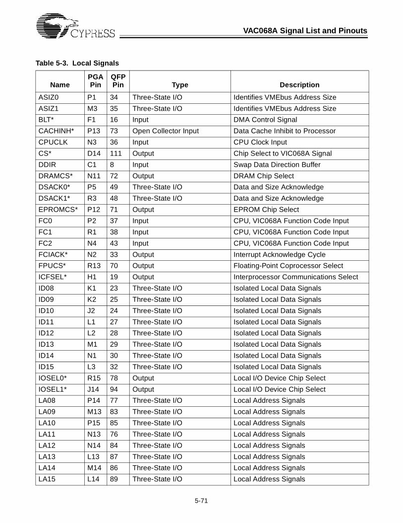
VAC068A Signal List and Pinouts
5-71
Table 5-3. Local Signals
NamePGAPin
QFPPin Type Description
ASIZ0 P1 34 Three-State I/O Identifies VMEbus Address Size
ASIZ1 M3 35 Three-State I/O Identifies VMEbus Address Size
BLT* F1 16 Input DMA Control Signal
CACHINH* P13 73 Open Collector Input Data Cache Inhibit to Processor
CPUCLK N3 36 Input CPU Clock Input
CS* D14 111 Output Chip Select to VIC068A Signal
DDIR C1 8 Input Swap Data Direction Buffer
DRAMCS* N11 72 Output DRAM Chip Select
DSACK0* P5 49 Three-State I/O Data and Size Acknowledge
DSACK1* R3 48 Three-State I/O Data and Size Acknowledge
EPROMCS* P12 71 Output EPROM Chip Select
FC0 P2 37 Input CPU, VIC068A Function Code Input
FC1 R1 38 Input CPU, VIC068A Function Code Input
FC2 N4 43 Input CPU, VIC068A Function Code Input
FCIACK* N2 33 Output Interrupt Acknowledge Cycle
FPUCS* R13 70 Output Floating-Point Coprocessor Select
ICFSEL* H1 19 Output Interprocessor Communications Select
ID08 K1 23 Three-State I/O Isolated Local Data Signals
ID09 K2 25 Three-State I/O Isolated Local Data Signals
ID10 J2 24 Three-State I/O Isolated Local Data Signals
ID11 L1 27 Three-State I/O Isolated Local Data Signals
ID12 L2 28 Three-State I/O Isolated Local Data Signals
ID13 M1 29 Three-State I/O Isolated Local Data Signals
ID14 N1 30 Three-State I/O Isolated Local Data Signals
ID15 L3 32 Three-State I/O Isolated Local Data Signals
IOSEL0* R15 78 Output Local I/O Device Chip Select
IOSEL1* J14 94 Output Local I/O Device Chip Select
LA08 P14 77 Three-State I/O Local Address Signals
LA09 M13 83 Three-State I/O Local Address Signals
LA10 P15 85 Three-State I/O Local Address Signals
LA11 N13 76 Three-State I/O Local Address Signals
LA12 N14 84 Three-State I/O Local Address Signals
LA13 L13 87 Three-State I/O Local Address Signals
LA14 M14 86 Three-State I/O Local Address Signals
LA15 L14 89 Three-State I/O Local Address Signals

VAC068A Signal List and Pinouts
5-72
LA16 N15 88 Three-State I/O Local Address Signals
LA17 K14 92 Three-State I/O Local Address Signals
LA18 M15 90 Three-State I/O Local Address Signals
LA19 K15 96 Three-State I/O Local Address Signals
LA20 L15 93 Three-State I/O Local Address Signals
LA21 J15 97 Three-State I/O Local Address Signals
LA22 H14 98 Three-State I/O Local Address Signals
LA23 H15 99 Three-State I/O Local Address Signals
LA24 G14 104 Three-State I/O Local Address Signals
LA25 G15 102 Three-State I/O Local Address Signals
LA26 F14 105 Three-State I/O Local Address Signals
LA27 F15 103 Three-State I/O Local Address Signals
LA28 E15 107 Three-State I/O Local Address Signals
LA29 F13 106 Three-State I/O Local Address Signals
LA30 C15 110 Three-State I/O Local Address Signals
LA31 E14 108 Three-State I/O Local Address Signals
LD16 P6 52 Three-State I/O Local Data Signals
LD17 R6 56 Three-State I/O Local Data Signals
LD18 P7 54 Three-State I/O Local Data Signals
LD19 R4 50 Three-State I/O Local Data Signals
LD20 R7 57 Three-State I/O Local Data Signals
LD21 R5 53 Three-State I/O Local Data Signals
LD22 P8 58 Three-State I/O Local Data Signals
LD23 N7 55 Three-State I/O Local Data Signals
LD24 N8 60 Three-State I/O Local Data Signals
LD25 R8 59 Three-State I/O Local Data Signals
LD26 R9 62 Three-State I/O Local Data Signals
LD27 P9 64 Three-State I/O Local Data Signals
LD28 R10 63 Three-State I/O Local Data Signals
LD29 P10 65 Three-State I/O Local Data Signals
LD30 R11 67 Three-State I/O Local Data Signals
LD31 P11 68 Three-State I/O Local Data Signals
LADO D3 3 Input Latch VMEbus Address Out Signal
LADI E1 13 Input Latch Local Address In Signal
LAEN P3 44 Input Local Address Bus Enable Signal
Table 5-3. Local Signals (continued)
NamePGAPin
QFPPin Type Description

VAC068A Signal List and Pinouts
5-73
LBR* G3 15 Input Local Bus Request to VIC068A Signal
LDMACK* E3 7 Output Local DMA is in Progress
MWB* R12 69 Output Module Wants Local Bus Signal
PAS* R2 45 Input Processor Address Strobe
PIO0/TXDA C11 127 Three-State I/O General-Purpose I/O or UART A Transmit Signal
PIO1/RXDA B12 126 Three-State I/O General-Purpose I/O or UART A Receive Signal
PIO2/TXDB A14 125 Three-State I/O General-Purpose I/O or UART B Transmit Signal
PIO3/RXDB B13 124 Three-State I/O General-Purpose I/O or UART B Receive Signal
PIO4/IORD* F2 12 Three-State I/O General-Purpose I/O or I/O Read Signal
PIO5/IOWR* C12 123 Three-State I/O General-Purpose I/O or I/O Write Signal
PIO6/IOSEL3*
B14 117 Three-State I/O General-Purpose I/O or I/O Select 3 Signal
PIO7/Interrupt
C13 116 Three-State I/O General-Purpose I/O or Interrupt Request Signal
PIO8/IOSEL4*
D13 115 Three-State I/O General-Purpose I/O or I/O Select 4 Signal
PIO9/IOSEL5*
B15 114 Three-State I/O General-Purpose I/O or I/O Select 5 Signal
PIO10/Interrupt
C14 113 Three-State I/O General-Purpose I/O or Interrupt Request Signal
PIO11/Interrupt
D1 10 Three-State I/O General-Purpose I/O or Interrupt Request Signal
PIO12/SHRCS*
D15 109 Three-State I/O General-Purpose I/O or Shared Resources Chip Select Signal
PIO13/IOSEL2*
B1 5 Three-State I/O General-Purpose I/O or I/O Select 2 Signal
REFGT* G1 17 Output Refresh Grant Signal
RESET* R14 74 Input System Reset Signal
R/W* P4 46 Input Read/Write Signal
SLSEL0* H2 18 Output Slave Select 0 Signal
SLSEL1* J1 22 Output Slave Select 1 Signal
SWDEN* C2 4 Input Swap Data Enable Signal
VSBSEL* G2 14 Output VSB Chip Select Signal
WORD* M2 31 Output 16-Bit Data Access Signal
Table 5-3. Local Signals (continued)
NamePGAPin
QFPPin Type Description

VAC068A Signal List and Pinouts
5-74
Table 5-4. Power Supply Signals [1]
NamePGAPin Type Description
VDD A15 Input Power Input
VDD C5 Input Power Input
VDD C7 Input Power Input
VDD C9 Input Power Input
VDD H3 Input Power Input
VDD Core H13 Input Power Input
VDD J13 Input Power Input
VDD N5 Input Power Input
VDD N10 Input Power Input
VDD Input Power Input
VDD Input Power Input
VDD Input Power Input
VDD Input Power Input
VDD Input Power Input
VDD Input Power Input
VSS C4 Input Ground
VSS C6 Input Ground
VSS C8 Input Ground
VSS C10 Input Ground
VSS E13 Input Ground
VSS F3 Input Ground
VSS G13 Input Ground
VSS Core J3 Input Ground
VSS K3 Input Ground
VSS N6 Input Ground
VSS N9 Input Ground
VSS N12 Input Ground
VSS K13 Input Ground
VSS Input Ground
VSS Input Ground
VSS Input Ground

VAC068A Signal List and Pinouts
5-75
Note:
1. For QFP power supply signals, see .
VSS Input Ground
VSS Input Ground
VSS Input Ground
VSS Input Ground
VSS Input Ground
Table 5-4. Power Supply Signals [1] (continued)
NamePGAPin Type Description

VAC068A Signal List and Pinouts
5-76
.
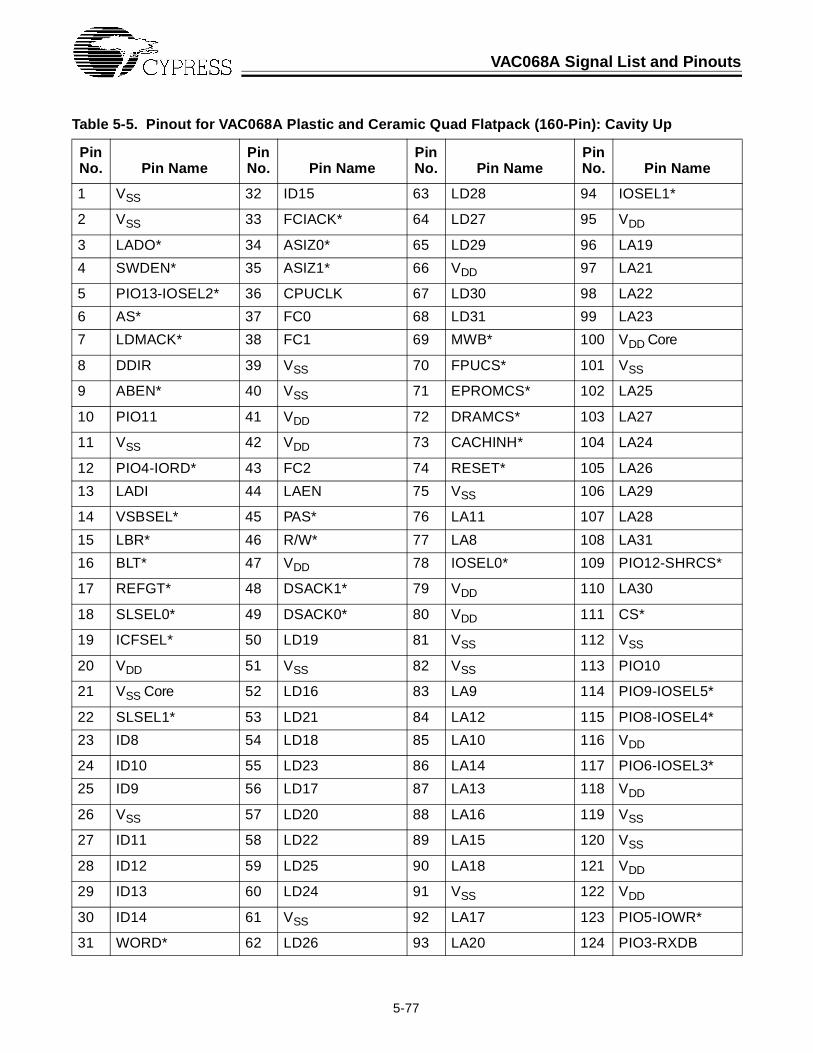
VAC068A Signal List and Pinouts
5-77
Table 5-5. Pinout for VAC068A Plastic and Ceramic Quad Flatpack (160-Pin): Cavity Up
Pin No. Pin Name
Pin No. Pin Name
Pin No. Pin Name
Pin No. Pin Name
1 VSS 32 ID15 63 LD28 94 IOSEL1*
2 VSS 33 FCIACK* 64 LD27 95 VDD
3 LADO* 34 ASIZ0* 65 LD29 96 LA19
4 SWDEN* 35 ASIZ1* 66 VDD 97 LA21
5 PIO13-IOSEL2* 36 CPUCLK 67 LD30 98 LA22
6 AS* 37 FC0 68 LD31 99 LA23
7 LDMACK* 38 FC1 69 MWB* 100 VDD Core
8 DDIR 39 VSS 70 FPUCS* 101 VSS
9 ABEN* 40 VSS 71 EPROMCS* 102 LA25
10 PIO11 41 VDD 72 DRAMCS* 103 LA27
11 VSS 42 VDD 73 CACHINH* 104 LA24
12 PIO4-IORD* 43 FC2 74 RESET* 105 LA26
13 LADI 44 LAEN 75 VSS 106 LA29
14 VSBSEL* 45 PAS* 76 LA11 107 LA28
15 LBR* 46 R/W* 77 LA8 108 LA31
16 BLT* 47 VDD 78 IOSEL0* 109 PIO12-SHRCS*
17 REFGT* 48 DSACK1* 79 VDD 110 LA30
18 SLSEL0* 49 DSACK0* 80 VDD 111 CS*
19 ICFSEL* 50 LD19 81 VSS 112 VSS
20 VDD 51 VSS 82 VSS 113 PIO10
21 VSS Core 52 LD16 83 LA9 114 PIO9-IOSEL5*
22 SLSEL1* 53 LD21 84 LA12 115 PIO8-IOSEL4*
23 ID8 54 LD18 85 LA10 116 VDD
24 ID10 55 LD23 86 LA14 117 PIO6-IOSEL3*
25 ID9 56 LD17 87 LA13 118 VDD
26 VSS 57 LD20 88 LA16 119 VSS
27 ID11 58 LD22 89 LA15 120 VSS
28 ID12 59 LD25 90 LA18 121 VDD
29 ID13 60 LD24 91 VSS 122 VDD
30 ID14 61 VSS 92 LA17 123 PIO5-IOWR*
31 WORD* 62 LD26 93 LA20 124 PIO3-RXDB

VAC068A Signal List and Pinouts
5-78
125 PIO2-TXDB 134 A24 143 A12 152 VDD
126 PIO1-RXDA 135 VDD 144 A11 153 A19
127 PIO0-TXDA 136 A27 145 A13 154 A20
128 A30 137 A25 146 VSS 155 VSS
129 A28 138 A9 147 A14 156 A21
130 A31 139 A8 148 A15 157 A22
131 VSS 140 VSS 149 A16 158 A23
132 A26 141 VDD 150 A17 159 VDD
133 A29 142 A10 151 A18 160 VDD
Table 5-5. Pinout for VAC068A Plastic and Ceramic Quad Flatp ack (160-Pin): Cavity Up (continued)
Pin No. Pin Name
Pin No. Pin Name
Pin No. Pin Name
Pin No. Pin Name
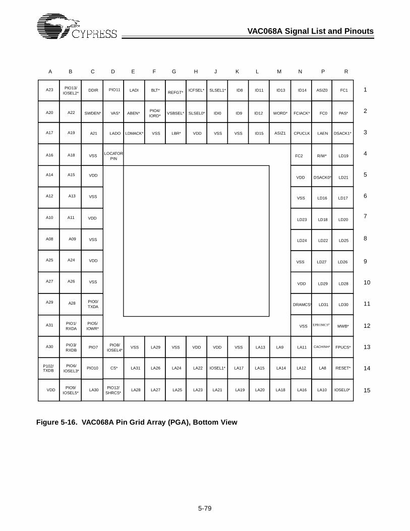
VAC068A Signal List and Pinouts
5-79
Figure 5-16. VAC068A Pin Grid Array (PGA), Bottom View
A B C D E F G H J K L M N P R
1
2
3
4
5
6
9
10
11
12
13
14
15
7
8
A23
A20
A17
A16
A14
A12
A10
A08
A25
A27
A29
A31
A30
P102/TXDB
VDD
A22
A19
A18
A15
A13
A11
A09
A24
A26
A28
PIO13/IOSEL2*
PIO1/RXDA
PIO3/RXDB
PIO6/IOSEL3*
PIO9/IOSEL5*
DDIR
SWDEN*
A21
VSS
VDD
VSS
VDD
VSS
VDD
VSS
PIO0/TXDA
PIO5/IOWR*
PIO7
PIO10
LA30
PIO11
VAS*
LADO
LOCATORPIN
PIO8/IOSEL4*
CS*
PIO12/SHRCS*
LADI
ABEN*
LDMACK*
BLT*
PIO4/IORD*
VSS
VSS
LA31
LA28
LA29
LA26
LA27
REFGT*
VSBSEL*
LBR*
VSS
LA24
LA25
ICFSEL*
SLSEL0*
VDD
VDD
LA22
LA23
SLSEL1*
IDI0
VSS
VDD
IOSEL1*
LA21
ID8
ID9
VSS
VSS
LA17
LA19
ID11
ID12
ID15
LA13
LA15
LA20
ID13
WORD*
ASIZ1
LA9
LA14
LA18
ID14
FCIACK*
CPUCLK
FC2
VDD
VSS
LD23
LD24
VSS
VDD
DRAMCS*
VSS
LA11
LA12
LA16
ASIZ0
FC0
LAEN
R/W*
DSACK0*
LD16
LD18
LD22
LD27
LD29
LD31
EPROMCS*
CACHINH*
LA8
LA10
FC1
PAS*
DSACK1*
LD19
LD21
LD17
LD20
LD25
LD26
LD28
LD30
MWB*
FPUCS*
RESET*
IOSEL0*

VAC068A Signal List and Pinouts
5-80
Figure 5-17. VAC068A Quad Flatpack (QFP), Top View
1VSS 120 VSS2VSS 119 VSS3LADO* 118 VDD4SWDEN* 117 PIO6-IOSEL3*5PIO13-IOSEL2* 116 VDD6AS* 115 PIO8-IOSEL4*7LDMACK* 114 PIO9-IOSEL5*8DDIR 113 PIO109ABEN* 112 VSS10PIO11 111 CS*11VSS 110 LA3012PIO4-IORD* 109 PIO12-SHRCS*13LADI 108 LA3114VSBSEL* 107 LA2815LBR* 106 LA2916BLT* 105 LA2617REFGT* 104 LA2418SLSEL0* 103 LA2719ICFSEL* 102 LA2520VDD 101 VSS21VSS 100 VDD22SLSEL1* 99 LA2323ID8 98 LA2224ID10 97 LA2125ID9 96 LA1926VSS 95 VDD27ID11 94 IOSEL1*28ID12 93 LA2029ID13 92 LA1730ID14 91 VSS31WORD* 90 LA1832ID15 89 LA1533FCIACK* 88 LA1634ASIZ0 87 LA1335ASIZ1 86 LA1436CPUCLK 85 LA1037FC0 84 LA1238FC1 83 LA939VSS 82 VSS40VSS 81 VSS
41V
DD
160
VD
D42
VD
D15
9V
DD
43F
C2
158
A23
44LA
EN
157
A22
45PA
S*
156
A21
46R
/W*
155
VS
S47
VD
D15
4A
2048
DS
AC
K1*
153
A19
49D
SA
CK
0*15
2V
DD
50LD
1915
1A
1851
VS
S15
0A
1752
LD16
149
A16
53LD
2114
8A
1554
LD18
147
A14
55LD
2314
6V
SS
56LD
1714
5A
1357
LD20
144
A11
58LD
2214
3A
1259
LD25
142
A10
60LD
2414
1V
DD
61V
SS
140
VS
S62
LD26
139
A8
63LD
2813
8A
964
LD27
137
A25
65LD
2913
6A
2766
VD
D13
5V
DD
67LD
3013
4A
2468
LD31
133
A29
69M
WB
*13
2A
2670
FP
UC
S*
131
VS
S71
EP
RO
MC
S*
130
A31
72D
RA
MC
S*
129
A28
73C
AC
HIN
H*
128
A30
74R
ES
ET
*12
7P
IO0-
TX
DA
75V
SS
126
PIO
1-R
XD
A76
LA11
125
PIO
2-T
XD
B77
LA8
124
PIO
3-R
XD
B78
IOS
EL0
*12
3P
IO5-
IOW
R*
79V
DD
122
VD
D80
VD
D12
1V
DD

5-81
5.8DC Performance Specifications
Table 5-6. VMEbus Signals (AS*, DS1*, DS0*, BCLR*, SYSCLK)
Parameter Description Test Conditions Comm. Industrial Military Units
VIH MinimumHigh-LevelInput Voltage
2.0 2.0 2.0 V
VIL MaximumLow-LevelInput Voltage
0.8 0.8 0.8 V
VOH MinimumHigh-LevelOutput Voltage
VCC = Min.,IOH = –3 mA
2.4 2.4 2.4 V
VOL MaximumLow-LevelOutput Voltage
VCC = Min.,IOL = 48 mA, 56 mA, 64 mA
0.6 0.6 0.6 V
IL MaximumInput LeakageCurrent
VCC = Max.,VIN = 0.6–2.4
±5 ±5 ±5 µA
VIK Input ClampVoltage
VCC = Min. IIN= –18 mA –1.2 –1.2 –1.2 V
VIK Input ClampVoltage
VCC = Min. IIN = 18 mA VCC+1.2 VCC+1.2 VCC+1.2 V
IOZ MaximumOutput LeakageCurrent
VCC = Max.GND < VOUT < VCCAll Outputs Disabled
±10 ±10 ±10 µA

Introduction to the VIC068A
5-82
Table 5-7. VMEbus Signals (Low Drive. All VMEbus Daisy-Chain Signals.)
Parameter Description Test Conditions Comm. Industrial Military Units
VIH MinimumHigh-LevelInput Voltage
2.0 2.0 2.0 V
VIL MaximumLow-LevelInput Voltage
0.8 0.8 0.8 V
VOH MinimumHigh-LevelOutput Voltage
VCC = Min.,IOH = –8 mA
2.4 2.4 2.4 V
VOL MaximumLow-LevelOutput Voltage
VCC = Min.,IOL = 8 mA
0.6 0.6 0.6 V
IL MaximumInput LeakageCurrent
VCC = Max.,VIN = 0.6–2.4
±5 ±5 ±5 µA
VIK Input ClampVoltage
VCC = Min. IIN= –18 mA –1.2 –1.2 –1.2 V
VIK Input ClampVoltage
VCC = Min. IIN = 18 mA VCC+1.2 VCC+1.2 VCC+1.2 V
IOZ MaximumOutput LeakageCurrent
VCC = Max.VOUT = 0.6/2.4VAll Outputs Disabled
±5 ±5 ±10 µA

Introduction to the VIC068A
5-83
Table 5-8. VMEbus Signals (Medium Drive. All non-High, non-Low Drive Signals, All VAC068A VMEbus Signals.)
Parameter Description Test Conditions Comm. Industrial Military Units
VIH MinimumHigh-LevelInput Voltage
2.0 2.0 2.0 V
VIL MaximumLow-LevelInput Voltage
0.8 0.8 0.8 V
VOH MinimumHigh-LevelOutput Voltage
VCC = Min.,IOH = –3 mA
2.4 2.4 2.4 V
VOL MaximumLow-LevelOutput Voltage
VCC = Min.,IOL = 48 mA
0.6 0.6 0.6 V
IL MaximumInput LeakageCurrent
VCC = Max.,VIN = 0.6–2.4
±5 ±5 ±5 µA
VIK Input ClampVoltage
VCC = Min. IIN=–18 mA –1.2 –1.2 –1.2 V
VIK Input ClampVoltage
VCC = Min. IIN = 18 mA VCC+1.2 VCC+1.2 VCC+1.2 V
IOZ MaximumOutput LeakageCurrent
VCC = Max.VOUT = 0.6/2.4VAll Outputs Disabled
±5 ±5 ±10 µA

Introduction to the VIC068A
5-84
Table 5-9. Non-VMEbus Signals
Table 5-10. Capacitance
Table 5-11. Operating Current
Parameter Description Test Conditions Comm. Industrial Military Units
VIH MinimumHigh-LevelInput Voltage
2.0 2.0 2.0 V
VIL MaximumLow-LevelInput Voltage
0.8 0.8 0.8 V
VOH MinimumHigh-LevelOutput Voltage
VCC = Min.,IOH = –8 mA
2.4 2.4 2.4 V
VOL MaximumLow-LevelOutput Voltage
VCC = Min.,IOL = 8 mA
0.6 0.6 0.6 V
IL MaximumInput LeakageCurrent
VCC = Max.,VIN = 0.00/VCC
±5 ±5 ±5 µA
VIK Input ClampVoltage
VCC = Min. IIN= –18 mA –1.2 –1.2 –1.2 V
VIK Input ClampVoltage
VCC = Min. IIN = 18 mA VCC+1.2 VCC+1.2 VCC+1.2 V
IOZ MaximumOutput LeakageCurrent
VCC = Max.GND < VOUT < VCCAll Outputs Disabled
±5 ±10 µA
Parameters Description Test Conditions Max. Units
CIN Input Capacitance TA = 25°C, f = 64 MHz,VCC = 5.0V
5 pF
COUT Output Capacitance 7 pF
Parameters Description Test Conditions Max. Units
IDD Maximum Operating Current
No external DC load 150 mA

5-85
5.9Package Diagrams
145-Pin Plastic Grid Array (Cavity Up) B144

Package Diagrams
5-86
145-Pin Grid Array (Cavity Up) G145

Package Diagrams
5-87
160-Lead Plastic Quad Flatpack N160
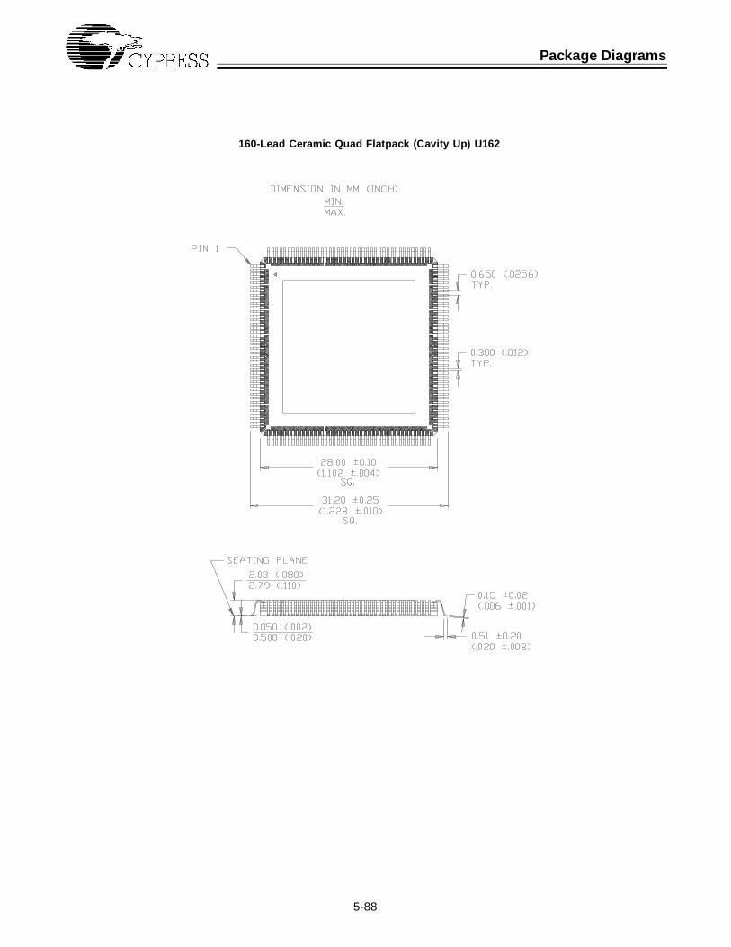
Package Diagrams
5-88
160-Lead Ceramic Quad Flatpack (Cavity Up) U162
G-1
Glossary
245 7400-family part type that is an 8-bit (octal) bus transceiver with controls fordirection and enabling of drivers.
543 7400-family part type that is an 8-bit (octal) bus transceiver with controls for latchenable, output enable, and direction flow.
68K A Motorola 68000, 68010, 68020, 68030 or 68040 microprocessor.
accelerated mode A mode of operation where the VIC068A will continuously assert the PAS* signalfor the duration of a DMA operation. The VIC068A expects the DSACK* signalto be continuously asserted for the duration of the DMA operation as well.
arbitration timeout A timeout that occurs when no module responds to a VMEbus bus grant.
assertion The forcing of a signal to its TRUE state.
base address The starting point of an address region defined by the mask register.
block tran sfer length The total length, in bytes, of a block transfer. In terms of the VIC068A, a blocktransfer may or may not contain more then one burst.
block tran sfer w/DMA A VIC068A block transfer mode in which the VIC068A obtains local bus master-ship and performs a VMEbus block transfer utilizing DMA on the local bus.
boundary crossing The crossing of a 256-byte local or VMEbus boundary during a block transfer.
buffer control signals VIC068A signals which control the operation of external address and data latch-es/buffers.
burst length The length, in VMEbus transfers, of a VMEbus block transfer burst. In terms ofthe VIC068A, there may or may not be more then one burst per block transfer.
byte An 8-bit unit of data.
clock-tick interrupt An optional, periodic interrupt issued by the VIC068A.
daisy-chain A type of VMEbus signal in which a signal level is propagated from board toboard starting from slot 1 and ending with the last occupied slot.
data size The size of a VMEbus data transfer independent of the physical bus size (byte,word, etc.).
deadlock In the context of the VIC068A, this is a condition where the local bus requiresthe use of the VMEbus and the VMEbus requires the use of the local bus. In thiscondition, the VIC068A requires the current local bus master remove its bustenure to let the VMEbus access proceed.

Glossary
G-2
deassertion The forcing of a signal to its FALSE state.
DMA Direct Memory Access. With the VAC068A, this refers to either DMA to theVMEbus or DMA to another interface controller.
DMAAT0 Module-based DMA Transfer Access Timing. The data acquisition timing theVIC068A uses for the first transfer of a module-based DMA transfer. This timingis programmed in bits 3-0 in the SSiCR1.
DMAAT1 Module-based DMA Transfer Access Timing. The data acquisition timing theVIC068A uses for the second and subsequent transfers of a module-based DMAtransfer. This timing is programmed in bits 7-4 in the SSiCR1.
DST The local data strobe minimum assertion timing. This timing is programmed inbit 4 of the LBTR.
dual-path A mode of operation which allows a single-cycle master operation to be per-formed by the VIC068A during interleave periods.
fair requester A VMEbus requester who waits until all requests on its particular VMEbus requestlevel are inactive before requesting the VMEbus.
Force EPROM A VAC068A mode of operation that asserts EPROMCS* after reset.
global switch A local interrupt issued by a VMEbus module to multiple VMEbus slaves.
IMAC Indivisible Multiple Address Cycle.
initiation cycle The local cycle which initiates a VMEbus block transfer with local DMA.
interleave period The period of time between block transfer bursts.
interprocessor communication facilities Various VIC068A register and facilities available by VMEbus accesses.
IPL Interrupt priority level.
ISAC Indivisible Single Address Cycle
local (local side) Resources that connect to the non-VMEbus signals of a VIC068A or VAC068A.
longword (lword) A 32-bit unit of data.
mail box An area of memory reserved for passing messages.
mask The comparison of only selected address bits for the purpose of specifying arange of don’t-care conditions.
master block transfer A mode of operation where the VIC068A performs a VMEbus block transfer.
master read The act of transferring data from a VMEbus slave to a VMEbus master.
master write The act of transferring data from a VMEbus master to a VMEbus slave
Glossary
G-3
master write posting A VMEbus master operation where the VIC068A captures outgoing VMEbuswrite data and acknowledges the local side immediately. This removes the VME-bus access time from local resources.
MBAT0 Master Block Transfer Access Timing. The data acquisition timing the VIC068Auses for the first transfer of a master block transfer with local DMA. This timingis programmed in bits 3-0 in the SSiCR1.
MBAT1 Master Block Transfer Access Timing. The data acquisition timing the VIC068Auses for the second and subsequent transfers of a master block transfer withlocal DMA. This timing is programmed in bits 7-4 in the SSiCR1.
module A VMEbus circuit card.
module-based DMA A mode of operation where the VIC068A transfers data from one local resourceto another utilizing DMA.
module switch A local interrupt issued by a VMEbus module to a single VMEbus slave.
MOVEM block transfer A VIC068A block transfer mode in which the local resource maintains local bus mas-tership while having the VIC068A perform transfers using block transfer protocol on theVMEbus.
non-accelerated mode A mode of operation where the VIC068A will toggle the PAS* signal for each transferof a DMA operation. The VIC068A expects the DSACK* signal to toggle for each transferof the DMA operation as well.
port size The physical size of the VMEbus modules data bus (D8, D16, D32, etc.)
pseudo cycle A block transfer with local DMA, initiation cycle
redirection Re-mapping VMEbus slave select address ranges to a specific local chip select output.
region An area of memory defined by one of three boundary registers in the VAC068A.
rescinding output A three-state output which is first driven High before it is three-stated.
RMC An indivisible read-modify-write cycle.
SAT Slave Access Timing. The data acquisition timing the VIC068A uses while performinga slave transfer. This timing is programmed in bits 3-0 in the SSiCR1.
SBAT0 Slave Block Transfer Access Timing. The data acquisition timing the VIC068A uses forthe first transfer of a slave block transfer. This timing is programmed in bits 3-0 in theSSiCR1.
SBAT1 Slave Block Transfer Access Timing. The data acquisition timing the VIC068A uses forthe second and subsequent transfers of a slave block transfer. This timing is pro-grammed in bits 7-4 in the SSiCR1.
self-access A condition where the VIC068A, as the VMEbus master, has selected itself as theVMEbus slave.

Glossary
G-4
slave block transfer A mode of operation where the VIC068A is slave to a VMEbus block transfer.
slave read The act of transferring data from a VMEbus slave to a VMEbus master.
slave write The act of transferring data from a VMEbus master to a VMEbus slave
slave write posting A VMEbus operation where the VIC068A captures incoming VMEbus write data andacknowledges the VMEbus immediately. This removes the local access time from VME-bus resources.
transfer timeout A timeout that occurs when no module responds with an acknowledge to a data transfer.
turbo A mode of operation in which the VIC068A reduces certain delays including set-uptimes.
UART Universal Asynchronous Receiver Transmitter.
VAC068A VMEbus Address Controller.
valid slave select A fully qualified request for slave operations.
VIC068A VMEbus Interface Controller.
VITA VMEbus International Trade Association.
VSB VMEbus Subsystem Bus.
word A 16-bit unit of data.


