84
VTA: Open & Flexible DL Acceleration Thierry Moreau TVM Conference, Dec 12th 2018

VTA: Open & Flexible DL Acceleration
Thierry MoreauTVM Conference, Dec 12th 2018

TVM Stack
High-Level Differentiable IR
Tensor Expression IR
LLVM CUDA Metal

TVM Stack
High-Level Differentiable IR
Tensor Expression IR
VTA: Open Hardware AcceleratorLLVM CUDA Metal

TVM Stack
High-Level Differentiable IR
Tensor Expression IR
VTA: Open Hardware AcceleratorLLVM CUDA Metal
Edge FPGA
TVM Stack
High-Level Differentiable IR
Tensor Expression IR
VTA: Open Hardware AcceleratorLLVM CUDA Metal
Edge FPGA Cloud FPGA

TVM Stack
High-Level Differentiable IR
Tensor Expression IR
VTA: Open Hardware AcceleratorLLVM CUDA Metal
Edge FPGA Cloud FPGA ASIC

TVM Stack
High-Level Differentiable IR
Tensor Expression IR
VTA: Open Hardware AcceleratorLLVM CUDA Metal
Edge FPGA Cloud FPGA ASIC

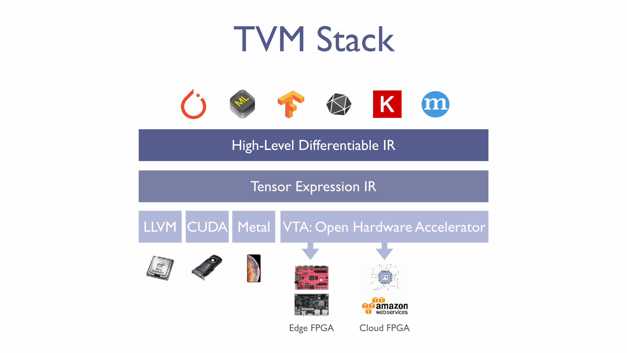
TVM Stack
Transparent End-to-End Deep Learning System Stack
High-Level Differentiable IR
Tensor Expression IR
VTA: Open Hardware AcceleratorLLVM CUDA Metal
Edge FPGA Cloud FPGA ASIC

TVM+VTA Stack Goals

TVM+VTA Stack Goals
• Blue-print for a complete deep learning acceleration stack

TVM+VTA Stack Goals
• Blue-print for a complete deep learning acceleration stack
• Experimentation framework for cross-stack deep learning optimizations

TVM+VTA Stack Goals
• Blue-print for a complete deep learning acceleration stack
• Experimentation framework for cross-stack deep learning optimizations
• Open-source community for industrial-strength deep learning acceleration

VTA Overview
Extensible Hardware Architecture
Programmability Across the Stack
Facilitates HW-SW Co-Design

VTA Overview
Extensible Hardware Architecture
Programmability Across the Stack
Facilitates HW-SW Co-Design

VTA: General DL Architecture

VTA: General DL Architecture
8
Tensor Intrinsic
x
8
8
8x
32
1
16
32vs.

VTA: General DL Architecture
8
Tensor Intrinsic
x
8
8
8x
32
1
16
32vs.
Hardware Datatype
<16 x i8> vs. <32 x i4>

VTA: General DL Architecture
8
Tensor Intrinsic
x
8
8
8x
32
1
16
32vs.
Memory Subsystem
vs.
Hardware Datatype
<16 x i8> vs. <32 x i4>

VTA: General DL Architecture
8
Tensor Intrinsic
x
8
8
8x
32
1
16
32vs.
Memory Subsystem
vs.
Hardware Datatype
<16 x i8> vs. <32 x i4>
Operation Support
{ADD, MUL, SHL, MAX} {ADD, SHL, MAX}vs.

VTA Hardware Architecture
Philosophy: simple hardware, provide software-defined flexibility

VTA Hardware Architecture
Philosophy: simple hardware, provide software-defined flexibility
DRAM
LOADMODULE
INPUT BUFFER
WEIGHT BUFFER
STORE BUFFER
MICRO-OP BUFFER
REGISTER FILE
Tensor Core
Vector ALU
LD→CMP Q
CMP→LD Q
CMP→ST Q
ST→CMP Q
COMPUTE MODULE
STOREMODULE
LOAD CMD Q
COMPUTE CMD Q
STORE CMD Q
INSTRUCTION FETCH MODULE

DRAM
LOADMODULE
INPUT BUFFER
WEIGHT BUFFER
STORE BUFFER
MICRO-OP BUFFER
REGISTER FILE
Tensor Core
Vector ALU
LD→CMP Q
CMP→LD Q
CMP→ST Q
ST→CMP Q
COMPUTE MODULE
STOREMODULE
LOAD CMD Q
COMPUTE CMD Q
STORE CMD Q
INSTRUCTION FETCH MODULE
VTA Hardware Architecture
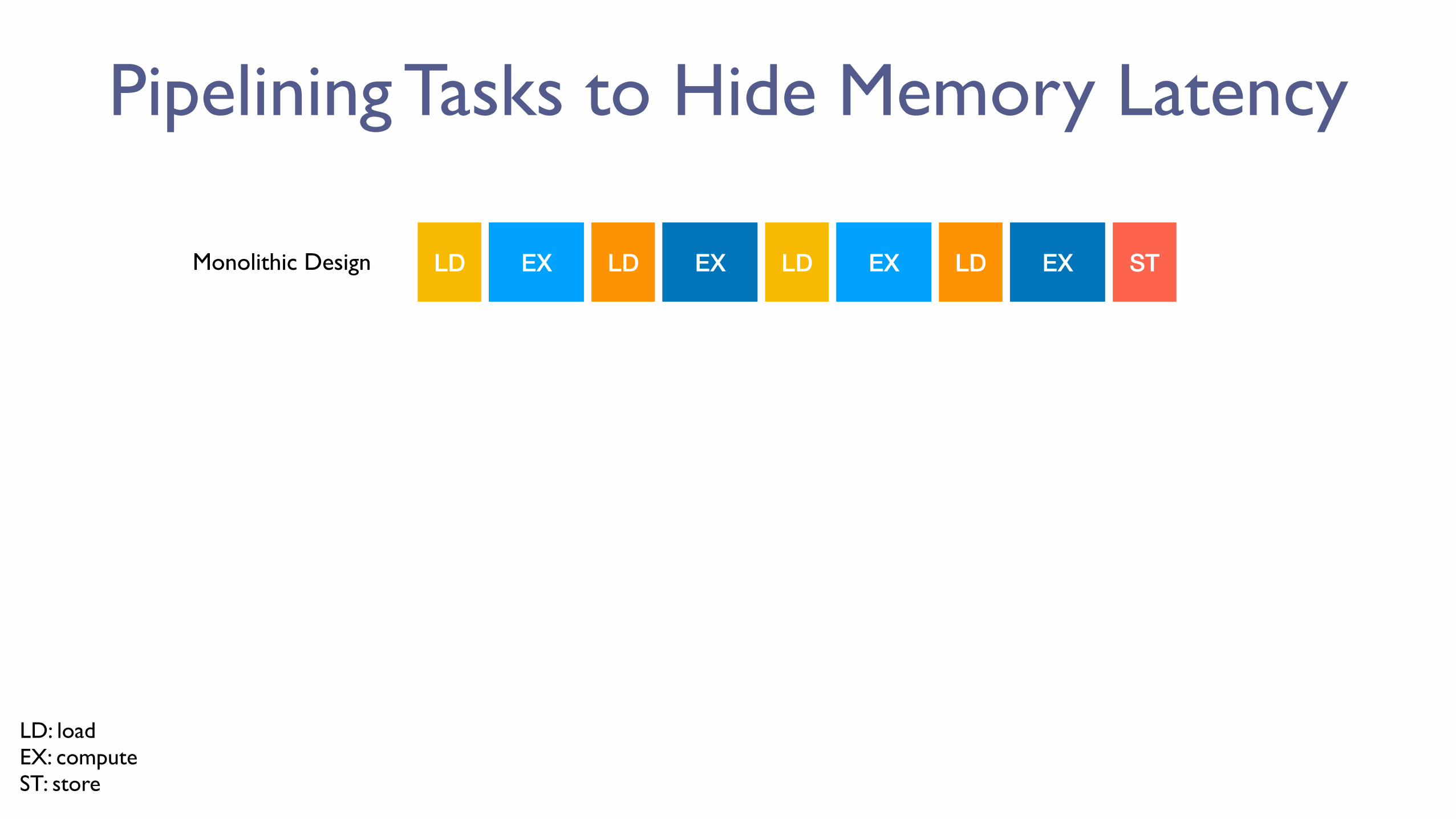
Pipelining Tasks to Hide Memory Latency
LD: loadEX: computeST: store
EXLD LD EX EXLD LD EX STMonolithic Design EXLD LD EX EX LD EX STLD

EXLD LD EX EXLD LD EX ST
Pipelining Tasks to Hide Memory Latency
Load Stage
Execute Stage
Store Stage
EX
LD LD
EX
LD
EX
LD
EX
ST
Monolithic Design
LD: loadEX: computeST: store

EXLD LD EX EXLD LD EX ST
Pipelining Tasks to Hide Memory Latency
Load Stage
Execute Stage
Store Stage
EX
LD LD
EX
LD
EX
LD
EX
ST
Monolithic Design
latency savings
LD: loadEX: computeST: store

EXLD LD EX EXLD LD EX ST
Pipelining Tasks to Hide Memory Latency
Load Stage
Execute Stage
Store Stage
EX
LD LD
EX
LD
EX
LD
EX
ST
Monolithic Design
latency savings
LD: loadEX: computeST: store
low-level synchronization between tasks is explicitly managed by the software

Two-Level ISA OverviewProvides the right tradeoff between expressiveness and code compactness

Two-Level ISA OverviewProvides the right tradeoff between expressiveness and code compactness
LOADDENSE STOREALU
• Use CISC instructions to perform multi-cycle tasks

Two-Level ISA OverviewProvides the right tradeoff between expressiveness and code compactness
LOADDENSE STOREALU
• Use CISC instructions to perform multi-cycle tasks
• Use RISC micro-ops to perform single-cycle tensor operations

Two-Level ISA OverviewProvides the right tradeoff between expressiveness and code compactness
LOADDENSE STOREALU
• Use CISC instructions to perform multi-cycle tasks
R0: R0 + GEMM(A8, W3)
• Use RISC micro-ops to perform single-cycle tensor operations

Two-Level ISA OverviewProvides the right tradeoff between expressiveness and code compactness
LOADDENSE STOREALU
• Use CISC instructions to perform multi-cycle tasks
R0: R0 + GEMM(A8, W3)
• Use RISC micro-ops to perform single-cycle tensor operations
R2: MAX(R0, ZERO)

VTA RISC Micro-Kernels

VTA RISC Micro-Kernelsmultiple RISC instructions define a micro-kernel,
which can be invoked by a CISC instruction

VTA RISC Micro-Kernelsmultiple RISC instructions define a micro-kernel,
which can be invoked by a CISC instruction
CONV2D: layout=NCHW, chan=128, kernel=(3,3), padding=(1,1), strides=(1,1)

VTA RISC Micro-Kernelsmultiple RISC instructions define a micro-kernel,
which can be invoked by a CISC instruction
CONV2D: layout=NCHW, chan=128, kernel=(3,3), padding=(1,1), strides=(1,1)
CONV2D: layout=NCHW, chan=256, kernel=(1,1), padding=(0,0), strides=(2,2)

VTA RISC Micro-Kernelsmultiple RISC instructions define a micro-kernel,
which can be invoked by a CISC instruction
CONV2D: layout=NCHW, chan=128, kernel=(3,3), padding=(1,1), strides=(1,1)
CONV2D_TRANSPOSE: ...
CONV2D: layout=NCHW, chan=256, kernel=(1,1), padding=(0,0), strides=(2,2)

VTA RISC Micro-Kernelsmultiple RISC instructions define a micro-kernel,
which can be invoked by a CISC instruction
CONV2D: layout=NCHW, chan=128, kernel=(3,3), padding=(1,1), strides=(1,1)
CONV2D_TRANSPOSE: ...
CONV2D: layout=NCHW, chan=256, kernel=(1,1), padding=(0,0), strides=(2,2)
GROUP_CONV2D: ...

VTA RISC Micro-Kernels
DCGAN ResNet50
micro-kernel programming gives us software-defined flexibility
“cat”

How is VTA Programmed?

How is VTA Programmed?// Pseudo-code for convolution program for the VIA accelerator// Virtual Thread 00x00: LOAD(PARAM[ 0-71]) // LD@TID00x01: LOAD(ACTIV[ 0-24]) // LD@TID00x02: LOAD(LDBUF[ 0-31]) // LD@TID00x03: PUSH(LD->EX) // LD@TID00x04: POP (LD->EX) // EX@TID00x05: EXE (ACTIV[ 0-24],PARAM[ 0-71],LDBUF[ 0-31],STBUF[ 0- 7]) // EX@TID00x06: PUSH(EX->LD) // EX@TID00x07: PUSH(EX->ST) // EX@TID00x08: POP (EX->ST) // ST@TID00x09: STOR(STBUF[ 0- 7]) // ST@TID00x0A: PUSH(ST->EX) // ST@TID0// Virtual Thread 10x0B: LOAD(ACTIV[25-50]) // LD@TID10x0C: LOAD(LDBUF[32-63]) // LD@TID10x0D: PUSH(LD->EX) // LD@TID10x0E: POP (LD->EX) // EX@TID10x0F: EXE (ACTIV[25-50],PARAM[ 0-71],LDBUF[32-63],STBUF[32-39]) // EX@TID10x10: PUSH(EX->LD) // EX@TID10x11: PUSH(EX->ST) // EX@TID10x12: POP (EX->ST) // ST@TID10x13: STOR(STBUF[32-39]) // ST@TID10x14: PUSH(ST->EX) // ST@TID1// Virtual Thread 20x15: POP (EX->LD) // LD@TID20x16: LOAD(PARAM[ 0-71]) // LD@TID20x17: LOAD(ACTIV[ 0-24]) // LD@TID20x18: LOAD(LDBUF[ 0-31]) // LD@TID20x19: PUSH(LD->EX) // LD@TID20x1A: POP (LD->EX) // EX@TID20x1B: POP (ST->EX) // EX@TID20x1C: EXE (ACTIV[ 0-24],PARAM[ 0-71],LDBUF[ 0-31],STBUF[ 0- 7]) // EX@TID20x1D: PUSH(EX->ST) // EX@TID20x1E: POP (EX->ST) // ST@TID20x1F: STOR(STBUF[ 0- 7]) // ST@TID2// Virtual Thread 30x20: POP (EX->LD) // LD@TID30x21: LOAD(ACTIV[25-50]) // LD@TID30x22: LOAD(LDBUF[32-63]) // LD@TID30x23: PUSH(LD->EX) // LD@TID30x24: POP (LD->EX) // EX@TID30x25: POP (ST->EX) // EX@TID20x26: EXE (ACTIV[25-50],PARAM[ 0-71],LDBUF[32-63],STBUF[32-39]) // EX@TID30x27: PUSH(EX->ST) // EX@TID30x28: POP (EX->ST) // ST@TID30x29: STOR(STBUF[32-39]) // ST@TID3
// Convolution access pattern dictated by micro-coded program.// Each register index is derived as a 2-D affine function.// e.g. idxrf = arfy+brfx+crf
0, where crf0 is specified by
// micro op 0 fields.for y in [0…i) for x in [0…j) rf[idxrf
0] += GEVM(act[idxact0], par[idxpar
0]) rf[idxrf
1] += GEVM(act[idxact1], par[idxpar
1]) … rf[idxrf
n] += GEVM(act[idxactn], par[idxpar
n])
(b) Convolution micro-coded program
// Max-pool, batch normalization and activation function// access pattern dictated by micro-coded program.// Each register index is derived as a 2D affine function.// e.g. idxdst = adsty+bdstx+cdst
0, where cdst0 is specified by
// micro op 0 fields.for y in [0…i) for x in [0…j) // max pooling rf[idxdst
0] = MAX(rf[idxdst0], rf[idxsrc
0]) rf[idxdst
1] = MAX(rf[idxdst1], rf[idxsrc
1]) … // batch norm rf[idxdst
m] = MUL(rf[idxdstm], rf[idxsrc
m]) rf[idxdst
m+1] = ADD(rf[idxdstm+1], rf[idxsrc
m+1]) rf[idxdst
m+2] = MUL(rf[idxdstm+2], rf[idxsrc
m+2]) rf[idxdst
m+3] = ADD(rf[idxdstm+3], rf[idxsrc
m+3]) … // activation rf[idxdst
n-1] = RELU(rf[idxdstn-1], rf[idxsrc
n-1]) rf[idxdst
n] = RELU(rf[idxdstn], rf[idxsrc
n])
(c) Max pool, batch norm and activationmicro-coded program
(a) Blocked convolution program with multiple thread contexts
Programming accelerators is
hard!!!

VTA Overview
Extensible Hardware Architecture
Programmability Across the Stack
Facilitates HW-SW Co-Design

Latency Hiding: An Example of Cross-Stack Design
programmer friendly construct// Virtual Threadingtx, co = s[OUT_L].split(co, factor=2)s[OUT_L].bind(tx, thread_axis(“cthread”))

Latency Hiding: An Example of Cross-Stack Design
programmer friendly construct// Virtual Threadingtx, co = s[OUT_L].split(co, factor=2)s[OUT_L].bind(tx, thread_axis(“cthread”))
low-level pipelined execution EX
LD LD
EX
LD
EX
LD
EX
ST

Latency Hiding: An Example of Cross-Stack Design
programmer friendly construct// Virtual Threadingtx, co = s[OUT_L].split(co, factor=2)s[OUT_L].bind(tx, thread_axis(“cthread”))
low-level pipelined execution EX
LD LD
EX
LD
EX
LD
EX
ST
?

Latency Hiding: An Example of Cross-Stack Design
programmer friendly construct
low-level pipelined execution

Latency Hiding: An Example of Cross-Stack Design
programmer friendly construct
low-level pipelined execution
Tensor Expression Optimizer (TVM) inserts dependence ops based on thread scope

Latency Hiding: An Example of Cross-Stack Design
programmer friendly construct
low-level pipelined execution
Tensor Expression Optimizer (TVM) inserts dependence ops based on thread scope
VTA Runtime & JIT Compiler generates instruction stream

Latency Hiding: An Example of Cross-Stack Design
programmer friendly construct
low-level pipelined execution
Tensor Expression Optimizer (TVM) inserts dependence ops based on thread scope
VTA Runtime & JIT Compiler generates instruction stream
VTA Hardware/Software Interface (ISA) exposes explicit dependences
VTA MicroArchitecture execution predicated on dependences
9-60% better compute utilization

VTA Helped inform ASIC Support in TVM

VTA Helped inform ASIC Support in TVM
1. How do we partition work and explicitly manage on-chip memories?
W
H
CI
W
H
CI
❌ not enough SRAM! ✅ fits in SRAM
// Tileyo, xo, yi, xi = s[OUT].tile(y, x, 4, 4)// Scoped cache readINP_L = s.cache_read(INP, vta.inp, [OUT])s[INP_L].compute_at(s[OUT], xo)

VTA Helped inform ASIC Support in TVM
1. How do we partition work and explicitly manage on-chip memories?
2. How do we take advantage of tensor computation intrinsics?W
H
CI
W
H
CI
❌ not enough SRAM! ✅ fits in SRAM
= x
// Tileyo, xo, yi, xi = s[OUT].tile(y, x, 4, 4)// Scoped cache readINP_L = s.cache_read(INP, vta.inp, [OUT])s[INP_L].compute_at(s[OUT], xo)
// Tensorizes[OUT_L].tensorize(ni)

VTA Helped inform ASIC Support in TVM
1. How do we partition work and explicitly manage on-chip memories?
2. How do we take advantage of tensor computation intrinsics?
3. How do we hide memory access latency?
W
H
CI
W
H
CI
❌ not enough SRAM! ✅ fits in SRAM
= x
// Tileyo, xo, yi, xi = s[OUT].tile(y, x, 4, 4)// Scoped cache readINP_L = s.cache_read(INP, vta.inp, [OUT])s[INP_L].compute_at(s[OUT], xo)
// Tensorizes[OUT_L].tensorize(ni)
// Virtual Threadingtx, co = s[OUT_L].split(co, factor=2)s[OUT_L].bind(tx, thread_axis(“cthread”))
EX
LD LD
EX
LD
EX
LD
EX
ST

VTA Overview
Extensible Hardware Architecture
Programmability Across the Stack
Facilitates HW-SW Co-Design

Hardware Exploration with VTA
HW / SW Constraints
FPGA# BRAMs
DRAM channels
logic resources
Model batch size
data types
channel width
Architecture Knobs
GEMM Intrinsic: e.g. (1,32) x (32,32) vs. (4,16) x (16,16)
# of units in tensor ALU : e.g. 32 vs. 16
BRAM allocation between buffers, register file, micro-op cache
Circuit Knobs
Circuit Pipelining: e.g. for GEMM core between [11, 20] stages
PLL Frequency Sweeps: e.g. 250 vs. 300 vs. 333MHz
{VTA Design Space
}VTA Candidate Designs
#1 Design AAA @ 307GOPs
#2 Design BBB @ 307GOPs
#3 Design CCC @ 307GOPs
#4 Design DDD @ 256GOPs
Needs to pass place & routeand pass timing closure
Deliverable
307 GOPs
256 GOPs
thro
ughp
ut
autotuning steps
Operator Performance AutoTuning
Tuned Operator Lib
VTA Design BBB
FPGA
Graph Optimizer
Model
cust
om

AutoTVM for Conv2D on Hardware Candidates

AutoTVM for Conv2D on Hardware Candidates

Schedule Exploration with VTA
HW / SW Constraints
FPGA# BRAMs
DRAM channels
logic resources
Model batch size
data types
channel width
Architecture Knobs
GEMM Intrinsic: e.g. (1,32) x (32,32) vs. (4,16) x (16,16)
# of units in tensor ALU : e.g. 32 vs. 16
BRAM allocation between buffers, register file, micro-op cache
Circuit Knobs
Circuit Pipelining: e.g. for GEMM core between [11, 20] stages
PLL Frequency Sweeps: e.g. 250 vs. 300 vs. 333MHz
{VTA Design Space
}VTA Candidate Designs
#1 Design AAA @ 307GOPs
#2 Design BBB @ 307GOPs
#3 Design CCC @ 307GOPs
#4 Design DDD @ 256GOPs
Needs to pass place & routeand pass timing closure
307 GOPs
256 GOPs
thro
ughp
ut
autotuning steps
Operator Performance AutoTuning
Deliverable
Tuned Operator Lib
VTA Design BBB
FPGA
Graph Optimizer
Model
cust
om

End-to-end Performance

End-to-end Performance
0
200
400
600
800
MobileNet ResNet-18 ResNet-34 ResNet-50 DCGAN
ARM Cortex A53 (TVM) Mali T860 (ARMCL) FPGA Ultra96 (VTA)

End-to-end Performance
0
200
400
600
800
MobileNet ResNet-18 ResNet-34 ResNet-50 DCGAN
ARM Cortex A53 (TVM) Mali T860 (ARMCL) FPGA Ultra96 (VTA)

End-to-end Performance
0
200
400
600
800
MobileNet ResNet-18 ResNet-34 ResNet-50 DCGAN
ARM Cortex A53 (TVM) Mali T860 (ARMCL) FPGA Ultra96 (VTA)

End-to-end Performance
0
200
400
600
800
MobileNet ResNet-18 ResNet-34 ResNet-50 DCGAN
ARM Cortex A53 (TVM) Mali T860 (ARMCL) FPGA Ultra96 (VTA)

End-to-end Performance
2.5x 4.7x6.0x
3.8x
11.48x0
200
400
600
800
MobileNet ResNet-18 ResNet-34 ResNet-50 DCGAN
ARM Cortex A53 (TVM) Mali T860 (ARMCL) FPGA Ultra96 (VTA)

End-to-end Performance
2.5x 4.7x6.0x
3.8x
11.48x0
200
400
600
800
MobileNet ResNet-18 ResNet-34 ResNet-50 DCGAN
ARM Cortex A53 (TVM) Mali T860 (ARMCL) FPGA Ultra96 (VTA)
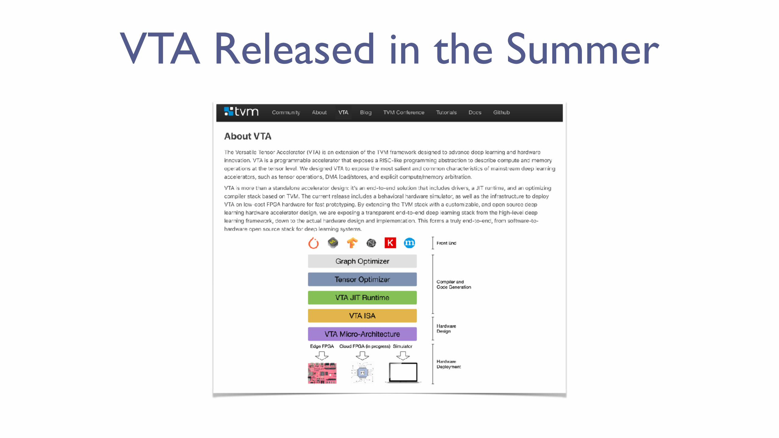
VTA Released in the Summer

VTA Demonstration
“cat”}Based on of the box FPGA demo & tutorials that you can try on your own!

VTA Demonstration

VTA Demonstration
pre-compiled bitstreampre-trained network model

VTA Demonstration
pre-compiled bitstreampre-trained network model

VTA Demonstration
pre-compiled bitstreampre-trained network model
TVM RPC
bitstreaminference module
data/params

VTA Demonstration
1. CPU Only Inference (ResNet34, W8)
2. VTA Inference (ResNet34, W8)
3. Fast VTA Inference (ResNet18, W4)

VTA Demonstration
1. CPU Only Inference (ResNet34, W8): 2.6 FPS
2. VTA Inference (ResNet34, W8): 10 FPS
3. Fast VTA Inference (ResNet18, W4): 19 FPS

TVM 0.5 VTA Release Features

TVM 0.5 VTA Release Features
• FPGA Support: Ultra96, ZCU102, Intel DE10Nano
• TOPI Operator Library & AutoTVM support
• Relay graph conversion front end, push-button 8bit quantization

2019 VTA Timeline

2019 VTA Timeline
• Q1:
• Chisel Generator for ASIC backends
• Initial Datacenter FPGA Prototype
• Q2:
• Novel Numerical Representation Support (Posit)
• Initial Training Prototype

More at tvm.ai/vta
Transparent End-to-End Deep Learning System Stack
High-Level Differentiable IR
Tensor Expression IR
VTA: Open Hardware AcceleratorLLVM CUDA Metal
Edge FPGA Cloud FPGA ASIC


