Page 1
W-Band Power Amplifier Design
Master's Thesis in Wireless, Photonics and Space Engineering
LI WEI
Department of Microtechnology and Nanoscience-MC2
Division of Microwave Electronics Laboratory
CHALMERS UNIVERSITY OF TECHNOLOGY
Göteborg, Sweden 2013
Page 3
MASTER'S THESIS IN WIRELESS, PHOTONICS AND SPACE ENGINEERING
W-Band Power Amplifier Design
Master's Thesis in Wireless, Photonics and Space Engineering
LI WEI
Department of Microtechnology and Nanoscience -MC2
Division of Microwave Electronics Laboratory
CHALMERS UNIVERSITY OF TECHNOLOGY
Göteborg, Sweden 2013
Page 4
W-Band Power Amplifier Design
LI WEI
© Li Wei, 2013
Technical report no XXXX:XX
Department of Microtechnology and Nanoscience - MC2
Division of Microwave Electronics Laboratory
Chalmers University of Technology
SE-412 96 Goteborg
Sweden
Telephone: + 46 (0)31-772 1000
Göteborg, Sweden 2013
Page 5
i
Abstract
This thesis presents two W-band power amplifiers (PA) in different processes: one is Teledyne
250 nm indium phosphide (InP) double-hetero-junction bipolar transistor (DHBT) process, and
the other is United Monolithic Semiconductors (UMS) 0.1 µm gallium arsenide (GaAs)
pseudomorphic high electron mobility transistor (pHEMT) process. Different power combining
topologies are investigated in these two designs. The bandwidth of the interstage matching
network is improved by a three-section quarter-wave transformer.
In the UMS 0.1 um GaAs pHEMT process, a three-stage PA is designed. Four 40 µm gate-
width transistors, each with six fingers, are paralleled by a planar spatial power combiner at the
output stage to improve the output power of the PA. The maximum gain of the PA is 14 dB. The
1 dB gain compression point (P1dB) is 21.2 dBm with 14.5% peak power added efficiency
(PAE).
In the Teledyne 250 nm InP DHBT process, a two-stage power amplifier is implemented.
Sixteen four-finger transistors of 10 µm emitter-length are paralleled at both input and output
stages to improve the P1dB. The gain of the PA is 12 dB. The P1dB is 23.8 dBm with 11.5% peak
PAE.
The two circuits are designed in Agilent Advanced Design System (ADS) with transistor and
capacitor models offered by the foundries. Transmission line networks for impedance matching,
power combining and power splitting are simulated in Momentum, a 2.5-D electromagnetic
(EM) software.
Keywords: power amplifier, InP, DHBT, HBT, GaAs, pHEMT, high electron mobility
transistor (HEMT), monolithic microwave integrated circuit (MMIC), W-band, bus-bar,
wideband
Page 7
iii
Contents
Abstract i
1. Introduction 1
2. MMIC Technology 3 2.1 Semiconductor Materials ................................................................................................... 3 2.2 Device Technologies .......................................................................................................... 4
2.2.1 Bipolar Junction Transistor (BJT)............................................................................. 4 2.2.2 Heterojunction Bipolar Transistor (HBT) ................................................................. 5 2.2.3 Metal-Oxide-Semiconductor Field-Effect Transistor (MOSFET) ............................ 6 2.2.4 Metal-Semiconductor Field Effect Transistor (MESFET) ........................................ 8 2.2.5 High-Electron-Mobility Transistor (HEMT) ............................................................ 9
3. Power Amplifiers 11 3.1 Power Amplifier Parameters ............................................................................................ 11
3.1.1 Gain ......................................................................................................................... 11 3.1.2 1 dB Gain Compression Point (P1dB)....................................................................... 12 3.1.3 Efficiency ................................................................................................................ 13
3.2 Power Amplifier Classification ........................................................................................ 13 3.2.1 Class A Power Amplifier ........................................................................................ 13 3.2.2 Class B Power Amplifier ........................................................................................ 14 3.2.3 Class AB and class C Power Amplifier .................................................................. 15
3.3 Power Combining Technologies ...................................................................................... 17 3.3.1 Wilkinson Power Combiner .................................................................................... 17 3.3.2 Bus-Bar Power Combiner ....................................................................................... 17 3.3.3 Directional Coupler ................................................................................................. 20 3.3.4 Marchand Balun ...................................................................................................... 21 3.3.5 Planar Spatial Power Combiner .............................................................................. 22
3.4 Power Amplifier Design Flow ......................................................................................... 24
4. Introduction of Processes 27 4.1 Teledyne 250 nm InP DHBT Process .............................................................................. 27
4.1.1 Substrates and Layer Distributions ......................................................................... 27 4.1.2 Passive Components ............................................................................................... 27 4.1.3 Transistors ............................................................................................................... 29
4.2 UMS 0.1 µm GaAs pHEMT Process ............................................................................... 30 4.2.1 Substrate and Layer Distribution ............................................................................ 30 4.2.2 Passive Components ............................................................................................... 30 4.2.3 Transistors ............................................................................................................... 31
5. Power Amplifier Design in Teledyne 250 nm InP DHBT Process 33 5.1 Single-Transistor Power Amplifier Design ...................................................................... 33
5.1.1 Device Selection ..................................................................................................... 33 5.1.2 Choice of Bias Point ............................................................................................... 35
Page 8
iv
5.1.3 In-Band Stability ..................................................................................................... 35 5.1.4 Optimization of Load and Source Impedances ....................................................... 36
5.2 Power Amplifier Topology .............................................................................................. 38 5.3 Matching Network Design ............................................................................................... 39
5.3.1 Output and Input Matching Networks .................................................................... 39 5.3.2 Interstage Matching Network ................................................................................. 40 5.3.3 In-Band Performances of the Sub-Circuit ............................................................... 43
5.4 Stabilizing and DC Feed Network Design ....................................................................... 44 5.4.1 Out-of-Band Stabilization ....................................................................................... 44 5.4.2 Cancellation of Odd-Mode Oscillation ................................................................... 45 5.4.3 DC Feed Network ................................................................................................... 46
5.5 Simulation Results and Layout ........................................................................................ 47 5.6 Test Circuit Design for Tape-Out .................................................................................... 50
5.6.1 Performance of Matching Networks ....................................................................... 50 5.6.2 Performance and Layout ......................................................................................... 51
6. Power Amplifier Design in UMS 0.1 µm GaAs pHEMT Process 55 6.1 Single-Transistor Power Amplifier Design ...................................................................... 55
6.1.1 Device Selection ..................................................................................................... 55 6.1.2 DC Bias Point Set and In-Band Stability ................................................................ 56 6.1.3 Optimization of Load and Source Impedances ....................................................... 56
6.2 Power Amplifier Topology .............................................................................................. 57 6.3 Matching Network Design ............................................................................................... 58
6.3.1 Input Matching Network ......................................................................................... 58 6.3.2 Output Matching Network ...................................................................................... 58 6.3.3 Interstage Matching Network ................................................................................. 60
6.4 Layout and Simulation Results ........................................................................................ 62 6.5 Comparison with a Reference Design .............................................................................. 64 6.6 Comparison with Published Results ................................................................................. 66
7. Conclusions and Future Work 69 7.1 Conclusions ...................................................................................................................... 69 7.2 Future Work ..................................................................................................................... 69
Acknowledgements 71
References 73
Page 9
1
Chapter 1
Introduction
The W-band (75 - 110 GHz) is mainly intended for satellite communications and remote
sensing [1-3]. A power amplifier with 25 dBm output power operating at 94-96 GHz is needed
in a terrestrial link [1]. In paper [2], a W-band spectroscopic system operating at
92-100 GHz is designed to realize high resolution remote sensing of particles and aerosols. In
this system, the 250 mW output power is achieved by THz1 multipliers but can be replaced by a
PA operating at W-band. It is also reported that W-band represents the best energetic trade-off
between water particle backscattering, forward scattering and cloud permeability, therefore a
W-band weather radar can be applied to improve the weather forecasting predictive models [3].
To fulfill the requirement of communication links with data rate of several GHz, channel
bandwidth of GHz is required, the mm-wave2 band provides such a potential [4]. In paper [5],
a 6 Gb/s E-band (60 - 90 GHz) system is demonstrated. It’s a trend for future mm-wave wireless
links because E-band links can transmit across many miles with air absorption less than
0.5 dB/km [4].
It’s predictable that the demand of W-band systems will grow in the future and the cost will
decrease. Power amplifier is one of the key components in a wireless transmitter. It determines a
transmitter’s maximum output power. In W-band, MMICs are mainly designed on GaAs- and
InP-based semiconductor materials. HEMT- and HBT-based devices show good power
performance [6]. The GaAs HEMT PA with the highest output power operating at W-band
reported saturation power of 0.35 W at 94 GHz [7]. An InP HEMT PA [8] has 427 mW
saturation power in W-band. Both of the two designs use planar spatial power combiner to
combine eight transistors at the output stage to improve output power. They were published in
the 1990s, but still hold the records of the highest output power in GaAs and InP HEMT
processes, respectively.
Recently, application of GaN HEMT is a new trend for mm-wave PA design. Due to its high
breakdown field, published designs have realized output power over 1 W [9, 10], and the drain
biases of transistors in [9] and [10] are 17.5 V and 14 V, respectively. These values are much
higher than those of GaAs- and InP-based devices. In the 0.35 W GaAs HEMT PA and the
427 mW InP HEMT PA, drain biases are 4 V and 2.5 V, respectively.
Complementary metal-oxide-semiconductor (CMOS) and silicon-germanium (SiGe)
BiCMOS technology are also moving forward to achieve good power amplification in W-band.
A current-combining, W-band PA in 65 nm CMOS was reported with 14 dB gain, 15 dBm
saturation power and 10% peak power added efficiency (PAE) [11]. In a 0.12 µm SiGe
BiCMOS process, a power amplifier operating at 77 GHz was reported with 17 dB gain, 17.5
dBm saturation power and 12.8% peak PAE [12].
Fig. 1.1 indicates that GaAs-based PAs operating at W-band with saturation power above
20 dBm is not common. The PA with the highest saturation power is still the one designed by
Wang in the 1990s [7]. Based on the 0.1 µm UMS GaAs pHEMT process, a power amplifier is
designed to touch the edge of power limitations in this thesis work.
1 wavelength of 1 mm to 0.1 mm in air, i.e. 300 GHz-3 THz
2 wavelength of 1 cm to 1 mm in air, i.e. 30 GHz-300 GHz
Page 10
1 INTRODUCTION
2
Based on the Teledyne 250 nm InP DHBT process, a power amplifier paralleling sixteen
transistors at output stage is designed to compare with the published 427 mW power amplifier
in InP HEMT technology [8].
In this thesis, two PAs are designed in ADS. Transmission-line matching and feed networks
are simulated in Momentum, a 2.5-D EM simulator. The extracted S-parameters of passive
networks and active device models are co-simulated in ADS.
Fig. 1.1: Saturated output power for MMIC PAs versus frequency. Source: [6].
This thesis focuses on the design of GaAs- and InP-based power amplifiers. In chapter 2,
semiconductor properties and transistor technologies are reviewed. In chapter 3, power
amplifier topologies and power combining technologies are introduced. In chapter 4, UMS and
Teledyne processes are involved. In chapter 5 and 6, the design of PA in Teledyne 250 nm InP
DHBT and UMS 0.1 µm GaAs pHEMT are explained and analyzed, respectively. In chapter 7,
simulation results are summarized with a prospect of future work.
Page 11
3
Chapter 2
MMIC Technology
Semiconductor materials and device technologies in monolithic microwave integrated circuit
(MMIC) are reviewed in this chapter. MMIC is an integrated circuit operating at microwave
frequencies1, where passive and active components are integrated on a single chip to implement
different functions such as power amplification, frequency conversion and signal generation.
With different semiconductor materials and device technologies, these functions can be realized
at different operating frequencies.
2.1 Semiconductor Materials
Group IV and group III-V semiconductors are materials commonly used in MMIC process.
Some semiconductor materials and their properties are listed in table 2.1 [13].
Table 2.1: Properties of IV and III-V semiconductor materials
Material Saturation
Velocity
(×107 cm s
-1)
Electron
Mobility
(cm2·V
-1·s
-1)
Bandgap
(eV)
Breakdown
Field
(×105 V·cm
-1)
Resistivity
(Ω cm-1
)
Dielectric
Constant
Si 1 900-1100 1.11 3 1000 11.8
SiGe 0.7 2000-3000 0.85 2 105
14.0
GaAs 1.2 5500-7000 1.43 6 108
12.5
GaN 2.5 400-1600 3.40 10 >1010
9.0
InP 0.67 < 5400 1.35 5 8.6×10⁷
12.5
GaAs and InP are widely used in mm-wave system designs due to their high saturation
velocities and high electron mobilities. For example, a 0.67 THz amplifier is designed in InP
HEMT [14]. To improve output power, GaN is preferred for its high breakdown field, as shown
in Table. 2.1. Recently, SiGe process has become a new trend for mm-wave applications. It
combines SiGe HBT and Si CMOS to form a SiGe BiCOMOS technology with frequency
responses better than Si CMOS [15].
1 wavelength of 1 m to 1 mm in air, i.e. 0.3 GHz-300 GHz
Page 12
2 MMIC TECHNOLOGY
4
2.2 Device Technologies
2.2.1 Bipolar Junction Transistor (BJT)
A bipolar junction transistor has two p-n junctions and three doped regions which are base,
emitter and collector. Two types of BJT transistors exist, p-n-p and n-p-n transistors. An n-p-n
transistor consists of a p-doped base between an n-doped emitter and collector. A p-n-p
transistor consists of an n-doped base between a p-doped emitter and collector. The n-p-n
transistor is used for the explanation of BJT working mechanisms in the following text.
An n-p-n transistor under forward-active operating mode is shown in Fig. 2.1a, where the
base-emitter p-n junction is forward-biased and the base-collector p-n junction is reverse-biased.
The band diagram of a forward-active operating n-p-n transistor is shown in Fig. 2.1b. In
forward-active operating mode, the Fermi level in the emitter (EFe) is higher than that in the
base (EFb), therefore electrons can flow from the emitter to the base. The distribution of minority
carriers in a forward-active n-p-n bipolar transistor is shown in Fig. 2.1c. The gradient of
minority carrier electron concentration forces the electrons from the emitter to go through the
base and diffuse into the collector. An equation to calculate the collector current density is given
[16]
, (2.1)
where nB0 is the density of electrons at the edge of the emitter close to the base, and ve is the
effective velocity of electrons.
Similarly, when an n-p-n BJT is forward biased, the hole current density (Jb) from base to
emitter can be expressed as [16]
, (2.2)
where pE0 is the density of holes at the edge of the emitter close to the base, and vh is the
effective velocity of holes. The definition of current gain can be expressed as [16]
(2.3)
, (2.4)
where nE and pB are concentrations of the emitter free electrons and the base holes, NCB and NCE
are the densities of states in conduction band of base and emitter, NVB and NVE are the densities
of states in valence band of base and emitter, ∆Vp and ∆Vn are the valence-band and
conduction-band energy differences between base and emitter, respectively. Eq. 2.3 indicates
that current gain can be improved by increasing the ratio of emitter to base doping concentration
(nE/pB) and enlarging the difference between ∆Vp and ∆Vn. In a homojunction n-p-n BJT, current
gain is maintained by the ratio of nE to pB, because its valence-band and conduction-band energy
difference is zero as shown in Fig. 2.1b.
Page 13
2 MMIC TECHNOLOGY
5
(a)
(b)
(c)
Fig. 2.1: (a) A forward-biased n-p-n BJT. (b) Band diagram of a forward-biased n-p-n BJT.
(c) Concentration of minority carriers in an n-p-n BJT.
2.2.2 Heterojunction Bipolar Transistor (HBT)
Different from a homojunction BJT, a heterojunction bipolar transistor improves its current
gain by increasing the bandgap difference (∆Eg) between base and emitter in Eq. 2.4. The band
diagram of an HBT is shown in Fig. 2.2a. The emitter bandgap is wider than the base bandgap.
With extra current gain from ∆Eg, seen from Eq. 2.3, a reduced doping ratio of nE to pB can still
retain a high current gain in an HBT. In Fig. 2.2b, base-doping level of an HBT is higher than
the emitter-doping level, which reduces a transistor’s base sheet resistance and therefore
improves its cut-off frequency [16].
Page 14
2 MMIC TECHNOLOGY
6
(a) (b)
Fig. 2.2: (a) Band diagram of an HBT. (b) A doping profile of an HBT.
2.2.3 Metal-Oxide-Semiconductor Field-Effect Transistor (MOSFET)
The main part of a MOSFET is a voltage-controlled inversion layer at the interface between
oxide and semiconductor. The mechanism of this inversion layer can be explained based on a
p-type MOS structure. As shown in Fig. 2.3a, in a p-type MOS structure, a positive voltage is
applied on the metal layer contacting with the oxide, therefore the conduction and valence bands
of the p-type semiconductor close to the oxide bend downward. With increased voltage on the
metal, the conduction band of the semiconductor approaches the Fermi level to generate an
n-channel inverion layer in a p-type semiconductor as shown in Fig. 2.3b. This inversion layer is
the electron transportation channel in an n-channel Metal-Oxide-Semiconductor Field-Effect
Transistor (NMOSFET).
(a) (b)
Fig. 2.3: (a) Band diagram of a p-type MOS structure under positive bias. (b) N-channel inversion layer in
a p-type MOS structure.
Page 15
2 MMIC TECHNOLOGY
7
In an NMOSFET, the n-type source and drain are connected to the two sides of the channel.
With positve voltage on the drain and zero bias on the source, electrons from the source flow
through the channel to the drain as shown in Fig. 2.4a.
(a) (b)
Fig. 2.4: (a) Schematic of a forward-biased NMOSFET, (b) A 3-D figure of an NMOSFET.
When a transistor is working in saturation region, i.e., VGS > VTH, VDS > VGS-VTH, a current-
voltage relationship can be expressed as [17]
. (2.5)
The current-voltage relationship for a transistor in nonsaturation region, i.e., VGS > VTH,
VDS < VGS-VTH, is given by [17]
, (2.6)
where µn is the electron mobility in an n-type channel, Cox is the oxide capacitance per unit area,
VTH is the threshold voltage of the transistor, W is the gate width and L is the channel length, as
shown in Fig. 2.4b.
Simliar to an NMOSFET, a p-channel MOSFET is realized by generating a p-channel
inversion layer in an n-type semiconductor. To implement these two transistors in an n-type
substrate, a p-well is made to support NMOS transistors, as shown in Fig. 2.5. This is the basic
principle in a Complementary Metal–Oxide–Semiconductor (CMOS) technology.
Fig. 2.5: Cross section of a NMOS and PMOS in CMOS technology.
Page 16
2 MMIC TECHNOLOGY
8
2.2.4 Metal-Semiconductor Field Effect Transistor (MESFET)
In a MESFET, a Schottky barrier is implemented between the gate and channel. The barrier
at the interface of the metal and semiconductor generates a depletion area as shwon in Fig. 2.6a.
With the reduction of gate bias, the depletion width is expanded to reduce the conduction
channel of the MESFET as shown in Fig. 2.6b. By controlling this depletion width, the current
flow from drain to source can be tuned. A simplified voltage-current model of MESFET can be
found as [18]
, (2.7)
where W is the gate width, h is the channel thickness, h(x) is the depletion width, Nd is the
doping concentration, µn is the electron mobility and
is the electron field pushing electron
along the channel.
(a) (b)
(c)
Fig. 2.6: (a) Band diagram of a GaAs MESFET. (b) Depletion expansion of a GaAs MESFET under
reduced gate bias. (c) A 3-D figure of a MESFET.
Page 17
2 MMIC TECHNOLOGY
9
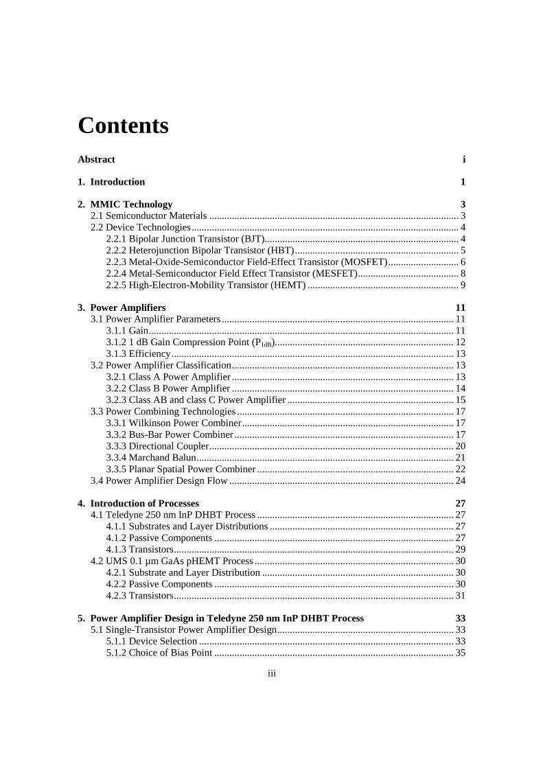
2.2.5 High-Electron-Mobility Transistor (HEMT)
The HEMT, also known as heterostructure field-effect transistor, is a type of FET utilizing
two semiconductor materials with different bandgaps to form a quantum well at material
interface.
Fig. 2.7a illustrates the band diagram of a GaAs HEMT. In this figure, bandgap of the
n-doped AlGaAs is larger than that of GaAs. Electrons in n-doped AlGaAs diffuse to the
undoped GaAs and bend the energy band at the GaAs/AlGaAs interface. These electrons
trapped in the quantum well have electron mobility (µn) higher than those in an n-doped
MESFET. It is because electrons in n-doped MESFET move in a channel with ionized donors as
shown in Fig. 2.7b. It limits the electron mobility due to the ionized impurity scattering [18]. In
a HEMT, the electron mobility is improved by separating electrons and the ionized donors as
shown in Fig. 2.7c. The drain current (ID) of a HEMT is given by [18]
, (2.8)
where ns is the electron density in the quantum well, ν(E) is the velocity of carriers under an
electrical field E, and W is the gate width.
(a)
(b)
(c)
Fig. 2.7: (a) Band diagram of a GaAs HEMT. (b) Electron transportation in MESFET. (c) Electron
transportation in HEMT.
Page 18
2 MMIC TECHNOLOGY
10
Page 19
11
Chapter 3
Power Amplifiers
In this chapter, PA parameters such as gain, 1 dB gain compression point (P1dB) and drain
efficiency are discussed. PAs of different classes are explained and compared. Moreover,
different power combining technologies are introduced. At the end of this chapter, a power
amplifier design flow is presented.
3.1 Power Amplifier Parameters
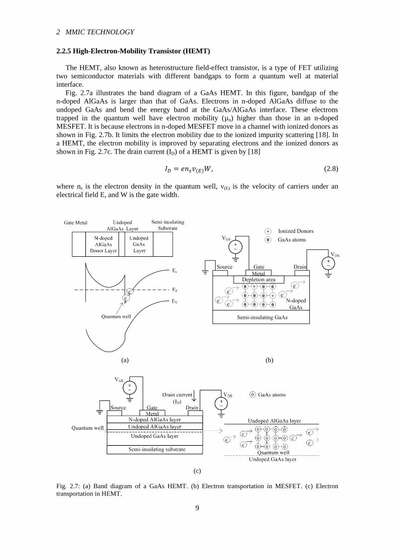
3.1.1 Gain
The gain of an amplifier is defined as the ratio of its output to input power
, (3.1)
where G is the gain of the amplifier in dB, Pout and Pin are output and input powers in W
respectively. When a relative small input power is injected into a PA, the gain of the amplifier is
independent of the input signal level. On the contrary, the gain of an amplifier drops when a
relative large input power is injected because of nonlinearities in the amplifier, as shown in
Fig. 3.1b.
(a) (b)
Fig. 3.1: (a) Schematic for gain measurement. (b) A plot of gain versus input power level.
Page 20
3 POWER AMPLIFIERS
12
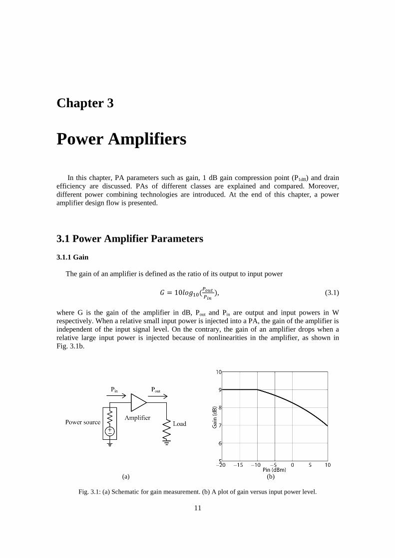
3.1.2 1 dB Gain Compression Point (P1dB)
As mentioned in Section 3.1.1, when the input power increases to some extent, the gain of
the amplifier declines due to nonlinearities. To characterize the linearity of an amplifier, P1dB is
defined as the output power level at which the gain of the amplifier is 1 dB lower than its small
signal gain, as shown in Fig. 3.2.
Fig. 3.2: Gain and output power of an amplifier versus its input power.
In a real circuit, to achieve a specified gain, two amplifiers may be cascaded, as shown in Fig
3.3a. In this circuit, P1dB of the two-stage amplifier depends on P1dB of the two amplifiers and
the gain of the amplifier at the second stage. To show their effects on system P1dB, a gain
function of an amplifier including gain compression effects is created
, (3.2)
where G is the gain of the single-stage amplifier, G0 represents the small signal gain of the
amplifier, Pin is the input power and Pin1dB is the input 1 dB gain compression point of the
amplifier. Hence, P1dB of this amplifier is (Pin1dB+G0-1). Gain and power in this equation are
expressed in dB and dBm, respectively. In Fig 3.3a, P1dB of the second stage is 5 dBm with
5 dB small signal gain at stage 1. Based on Eq. 3.2, P1dB of stage 1 and small signal gain of
stage 2 are swept to check their effects on system P1dB. From simulation results in Fig. 3.3b, the
system P1dB will be 2 dB lower than the P1dB of the single-stage amplifier, if the amplifier at
stage 2 only has 3 dB small signal gain with the same P1dB at stage 1.
Page 21
3 POWER AMPLIFIERS
13
(a) (b)
Fig. 3.3: (a) A two-stage, cascaded power amplifier. (b) System P1dB versus P1 and G2.
3.1.3 Efficiency
Another important factor in a power amplifier is the efficiency. Drain efficiency is defined as
the ratio between output power and the injected DC power [19]
, (3.3)
where Pout is the output power of the amplifier and Pdc is the DC power consumption of the
amplifier. The other definition to characterize the power conversion efficiency is Power Added
Efficiency (PAE). It is the ratio of difference between output and input power to the DC power
consumption [19]
, (3.4)
where Pout is the output power, Pin is the input power, Pdc is the DC power consumption and G is
the gain of the amplifier.
3.2 Power Amplifier Classification
3.2.1 Class A Power Amplifier
Class A power amplifier is a linear power amplifier. During a signal period, the transistor is
always conducting. Its output voltage and current are purely sinusoidal waves with linear
amplification of the input signal. To sufficiently utilize a transistor operating at class A, the
voltage and current swings at drain/collector of a transistor should be linearly maximized. The
maximum linear output power of a class A power amplifier is defined as [19]
, (3.5)
where Vmax is the breakdown voltage of a transistor, Vknee is the knee voltage and Imax is the
maximum current the transistor can tolerate. Fig. 3.4b shows the current-voltage (I-V) curve of
a transistor and a load line under class A bias. Fig. 3.4c shows the relative time-domain
Page 22
3 POWER AMPLIFIERS
14
waveform. Assuming Vknee = 0, the maximum drain efficiency of a class A power amplifier is
50% [19].
(a)
(b)
(c)
Fig. 3.4: (a) A class A power amplifier. (b) Load line of a class A power amplifier. (c) Drain/collector
current and voltage waveforms of a class A power amplifier.
3.2.2 Class B Power Amplifier
A transistor biased at class B operation is switched-on during half of a signal period and the
drain current is a half-cosine wave, as shown in Fig. 3.5a. Fig. 3.5b and Fig. 3.5c illustrate load
line and time-domain waveforms of a class B PA, respectively. The cosine-shaped voltage wave
in Fig. 3.5c is due to the L-C bandpass filter which filters out unwanted high-order harmonics
and keeps the fundamental components. The conduction angle of a class B power amplifier is 𝜋,
which can be seen in Fig. 3.5c. When Vknee = 0, the maximum drain efficiency of a class B
power amplifier is 78.5% [19].
Page 23
3 POWER AMPLIFIERS
15
(a)
(b)
(c)
Fig. 3.5: (a) A class B power amplifier. (b) Load line of a class B power amplifier. (c) Drain/collector
current and voltage waveforms of a class B power amplifier.
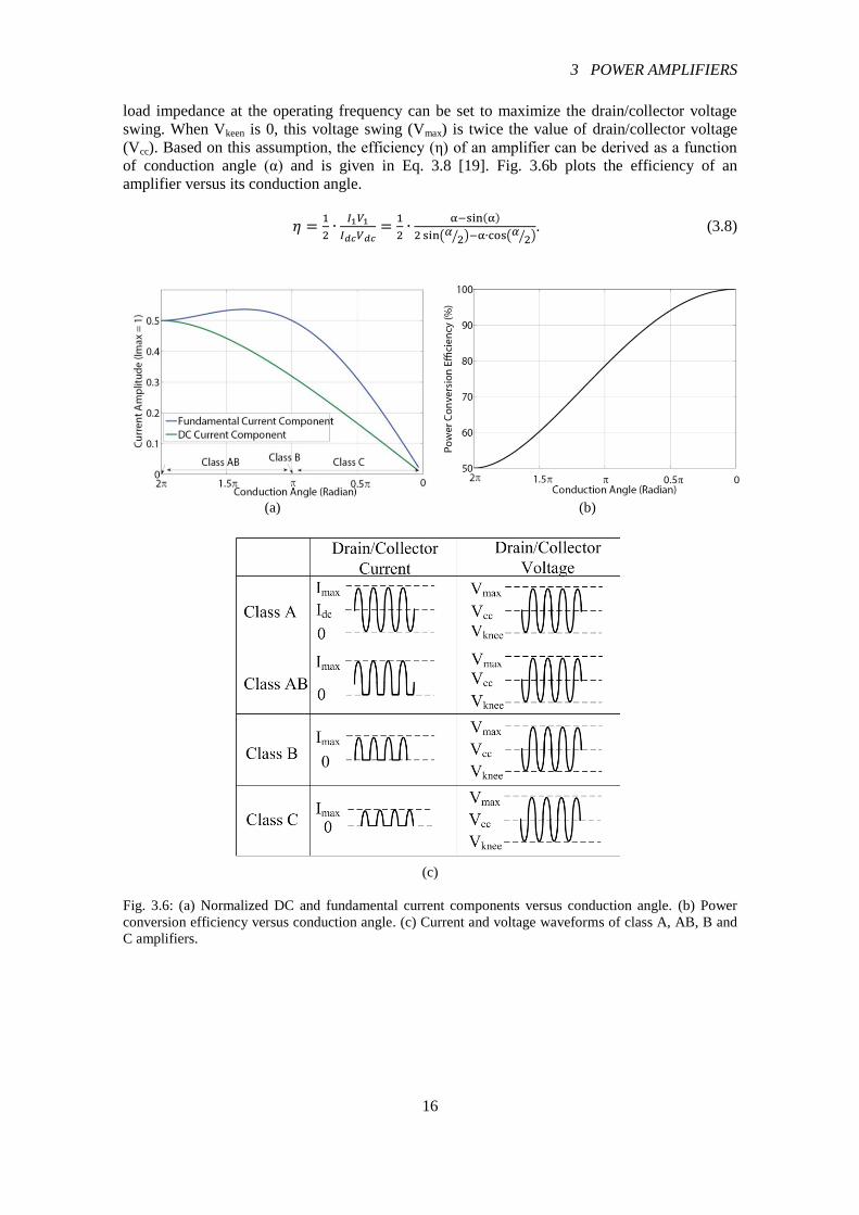
3.2.3 Class AB and class C Power Amplifier
A transistor biased in class AB has a conduction angle between 𝜋 and 2𝜋. Class C operation
reduces the conduction angle further to between 0 and 𝜋. Based on Fourier analysis, DC
component (Idc) and fundamental component (I1) of drain/collector current with conduction
angles between 0 and are plotted in Fig. 3.6a. The mathematical expressions of Idc and I1 are
given by [19]
( ⁄ ) ( ⁄ )
( ⁄ ) (3.6)
( ⁄ ), (3.7)
where Imax is the maximum current a transistor can tolerate and α is the conduction angle.
Current waveforms of different power amplifiers are shown in Fig. 3.6c. As the class B PA in
Fig. 3.5a, filters are inserted at the output network to filter out high-order harmonics and
generate output voltage with only DC and fundamental components. With known I1, optimum
Page 24
3 POWER AMPLIFIERS
16
load impedance at the operating frequency can be set to maximize the drain/collector voltage
swing. When Vkeen is 0, this voltage swing (Vmax) is twice the value of drain/collector voltage
(Vcc). Based on this assumption, the efficiency (η) of an amplifier can be derived as a function
of conduction angle (α) and is given in Eq. 3.8 [19]. Fig. 3.6b plots the efficiency of an
amplifier versus its conduction angle.
( ⁄ ) ( ⁄ ). (3.8)
(a)
(b)
(c)
Fig. 3.6: (a) Normalized DC and fundamental current components versus conduction angle. (b) Power
conversion efficiency versus conduction angle. (c) Current and voltage waveforms of class A, AB, B and
C amplifiers.
Page 25
3 POWER AMPLIFIERS
17
3.3 Power Combining Technologies
3.3.1 Wilkinson Power Combiner
In a Wilkinson power combiner, two input ports of the combiner are excited by signals in
phase, as shown in Fig. 3.7a. Odd mode signals at the two input ports are absorbed by the shunt
resistor. The S-matrix of an ideal Wilkinson power combiner can be expressed as [20]
[
]
√ [
] [
], (3.9)
where port 1 is the output port of the combiner, and ports 2 and 3 are input ports of the
combiner. To combine four transistors, a cascaded Wilkinson combiner, shown in Fig. 3.7b, can
be used. The insertion loss of a two-stage Wilkinson combiner is twice that of a single-stage
Wilkinson power combiner.
(a) (b)
Fig. 3.7: (a) A Wilkinson power combiner. (b) A cascaded Wilkinson power combiner.
3.3.2 Bus-Bar Power Combiner
In a bus-bar power combiner, all output ports of transistors are connected by a metal track as
shown in Fig. 3.8a. Following this metal track, matching elements are added to realize
impedance transformation and power combining. When the eight transistors in Fig. 3.8b are
excited in equal phase and amplitude, the phase and amplitude imbalances at the four output
nodes of the bus-bar power combiner are negligible [21]. This can be seen from Fig. 3.8b and
3.8c. The three symmetric lines in Fig. 3.8b are assumed to be “open-ports” when the eight
transistors are excited in equal phase and amplitude [21]. Hence, this bus-bar combining circuit
is equivalent to a parallel connection of four sub-blocks shown in Fig. 3.8c. Based on the
open-port approximation, in a practical design, the bus-bar combiner can be split and considered
as part of the output matching network as shown in Fig. 3.8d. When the sub-block of the output
matching network including split bus-bar network and matching lines is matched to N·Zc Ω, the
Page 26
3 POWER AMPLIFIERS
18
parallel connection of the N sub-blocks realizes an output impedance of Zc, as shown in Fig.
3.8d. The design of bus-bar matching network in this thesis work is based on this design
procedure.
(a) (b)
(c) (d)
Fig. 3.8: (a) A bus-bar power combiner with matching network. (b) A bus-bar power combiner with four
output nodes. (c) Equivalent sub-blocks of the bus-bar power combiner. (d) Design procedure of bus-bar
power combiner.
To prove the validity of the “open-ports” approximation, a bus-bar combiner paralleling
eight 30 Ω ports is designed and simulated in Momentum. The layout is shown in Fig. 3.9a with
equivalent circuit in Fig. 3.9b. It is designed on a substrate with thickness of 0.5 mm and
dielectric constant of 12.9. Simulation results of reflection and transmission coefficients in
Page 27
3 POWER AMPLIFIERS
19
Fig. 3.9c and phase delay in Fig. 3.9d. To test the power combining capability, eight input
signals with 1 mW each are injected into port 2-9 as shown in Fig. 3.9e. Output power at port 1
and insertion loss of this combining network is shown in Fig. 3.9f.
(a)
(b)
(c)
(d)
(e) (f)
Fig. 3.9: (a) Layout of the bus-bar combiner. (b) Equivalent circuit of the bus-bar power combiner. (c)
Reflection and transmission coefficients of the bus-bar power combiner. (d) Phase delay of the bus-bar
power combiner. (e) Bus-bar power combiner excited by eight 1 mW, in-phase signals. (f) Insertion loss
and output power of the combiner.
Page 28
3 POWER AMPLIFIERS
20
3.3.3 Directional Coupler
The directional coupler is a four-port microwave device. With reference to Fig. 3.10a, in an
ideal directional coupler, input signal from port 1 flows into ports 2 and 3 leaving port 4 isolated.
The two output signals at port 2 and port 3 are orthogonal. These can be explained by the
S-matrix of the directional coupler [20]
[
]
√ [
]
[
]
, (3.10)
where C1 and C2 are coupling coefficients of the directional coupler. For a lossless passive
diectional coupler
, (3.11)
where √
for a 3-dB directional coupler. Due to the reciprocal properity of a passive
component, a 3 dB directional coupler can run in reverse as a combiner. As an example, a
directional-coupler based power combiner designed at 10 GHz center frequency is simulated
with two 1 mW, orthogonal inputs at ports 2 and 3. The schematic is shown in Fig. 3.10b with
simulation results of output power at port 1 and insertion loss in Fig. 3.10c.
(a)
(b)
(c)
Fig. 3.10: (a) Schematic of directional coupler. (b) Directional coupler runs as a power combiner with 50
Ω terminals. (c) Output power and insertion loss of the directional-coupler based power combiner.
Page 29
3 POWER AMPLIFIERS
21
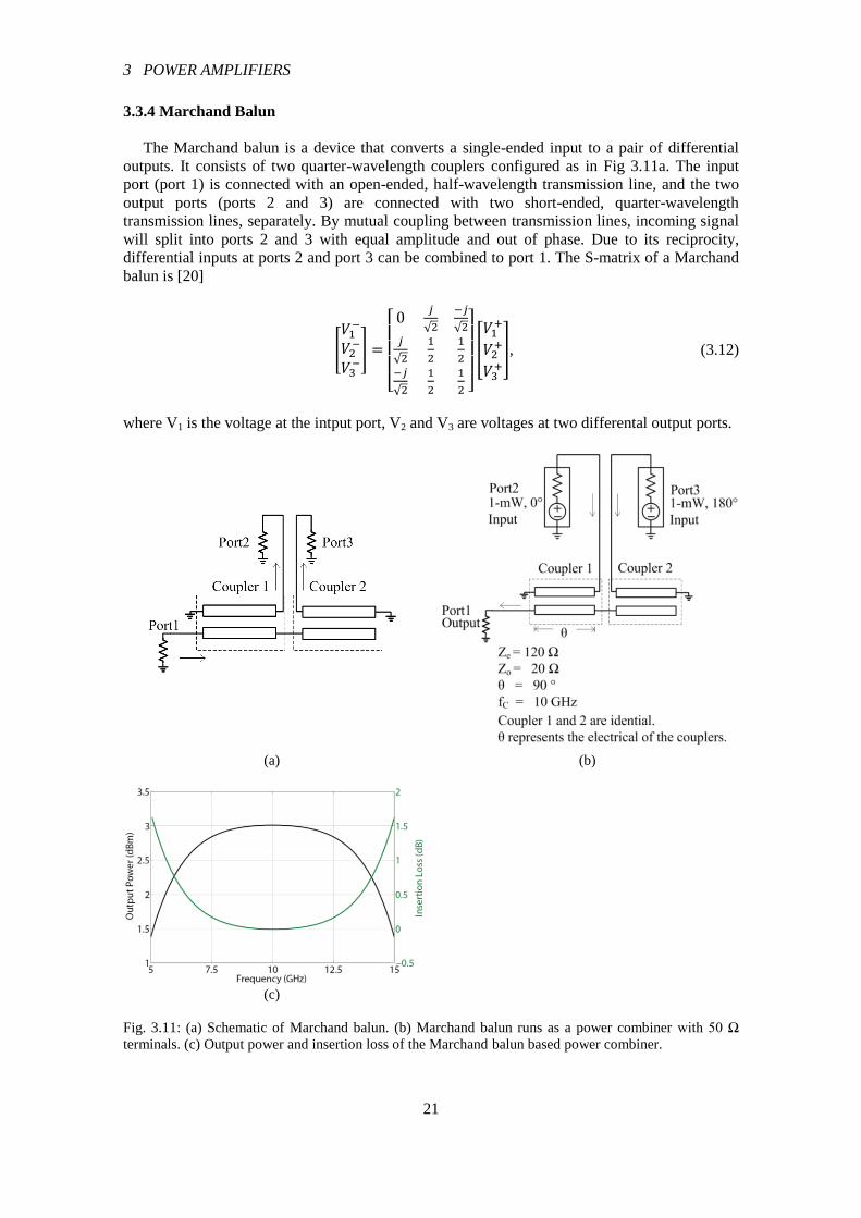
3.3.4 Marchand Balun
The Marchand balun is a device that converts a single-ended input to a pair of differential
outputs. It consists of two quarter-wavelength couplers configured as in Fig 3.11a. The input
port (port 1) is connected with an open-ended, half-wavelength transmission line, and the two
output ports (ports 2 and 3) are connected with two short-ended, quarter-wavelength
transmission lines, separately. By mutual coupling between transmission lines, incoming signal
will split into ports 2 and 3 with equal amplitude and out of phase. Due to its reciprocity,
differential inputs at ports 2 and port 3 can be combined to port 1. The S-matrix of a Marchand
balun is [20]
[
]
[
√
√
√
√
]
[
], (3.12)
where V1 is the voltage at the intput port, V2 and V3 are voltages at two differental output ports.
(a)
(b)
(c)
Fig. 3.11: (a) Schematic of Marchand balun. (b) Marchand balun runs as a power combiner with 50 Ω
terminals. (c) Output power and insertion loss of the Marchand balun based power combiner.
Page 30
3 POWER AMPLIFIERS
22
As an example, a Marchand balun designed at 10 GHz center frequency is excited by a pair
of 1 mW, differential signals. The schematic is shown in Fig. 3.11b. Simulated output power at
port 1 and insertion loss is shown in Fig. 3.11c.
3.3.5 Planar Spatial Power Combiner
Planar spatial power combiners offer the ability to parallel more than three transistors in one
stage [22]. To simplify the analysis, the following discussion will focus on the analysis of a
planar spatial power splitter. In Fig. 3.12a, the incoming wave from port 1 propogates into the
wide metal strip and splits into ports 2-5. The difficulty of designing such a power splitter is the
amplitude and phase balances between output ports, because the signal paths from port 1 to
other four ports are not identical. The unwanted phase and amplitude imbalances increase the
insertion loss of the planar spatial power combiner when it is ‘back-to-back’ connected for
power splitting and combining as shown in Fig. 3.12b.
To see the performance, a four-port planar spatial power combiner is implemented at 10 GHz
with schematic in Fig. 3.13a. It is designed on a substrate with thickness of 0.5 mm and
dielectric constant of 12.9. The transmisison coefficients and phase delays from port 1 to other
ports are plotted in Fig. 3.13b and Fig. 3.13c. Excited by four 1 mW, in-phase signal sources at
port 2-5, the output power at port 1 and insertion loss of the power combiner are plotted in
Fig. 3.14b with the schematic in Fig. 3.14a. Comparing data in Fig. 3.13b, 3.13c and 3.14b at
10 GHz, 0.5 dB amplitude imbalance and 3° phase imbalance only introduce an inseriton loss
lower than 0.1 dB.
Fig. 3.12: (a) Schematic of planar spatial power splitter/combiner. (b) Back-to-back connection of planar
spatial power splitter/combiner.
Page 31
3 POWER AMPLIFIERS
23
(a) (b)
(c)
Fig. 3.13: (a) Layout of a planar spatial power combiner. (b) Transmission coefficient and reflection
coefficient of the planar spatial power combiner. (c) Phase delay of the planar spatial power combiner.
(a) (b)
Fig. 3.14: (a) A planar spatial power combiner excited by four in-phase signal sources. (b) Output power
and insertion loss of the planar spatial power combiner.
Page 32
3 POWER AMPLIFIERS
24
3.4 Power Amplifier Design Flow
Device selection is the the first step of power amplifier design, as shwon in Fig. 3.15. It is a
synthesised consideration of the transistor’s gain, power capability and input/output impedance.
In a given process, the power capability of a transistor is proportional to its total gate width.
However, larger total gate width means lower maximum oscillation frequency (fmax) as the
improvement of total gate width is achieved by either increasing gate width of the transistor or
paralleling unit transistors to achieve a multi-finger one. In the first case, fmax of the transistor
decreases due to the parasitic connection losses as shown in Fig. 3.16a. In the second case, the
parallel connection of unit transistors introduces phase differences at gates and drains, therefore
degrades fmax of the multi-finger transistor as shown in Fig. 3.16b. Hence, the selection of
device size is a tradeoff between gain and power. For instance, comparing a transistor with
10 dB gain and 8 dBm P1dB and a transistor with 7 dB gain and 11 dBm P1dB, the latter one is
preferred at the output stage, because P1dB of the amplifier at the output stage dominates the
system P1dB. After the comparison between gain and P1dB, the input and output impedances of
the transistor are also considered. If the input/output impedance of a transistor is too low to
match to 50 Ω terminal by inserting matching networks, a transistor with higher input/output
impedance should be considered.
After the selection of the transistor, stability at the operating frequencies is analyzed. If the
transistor is not unconditionally stable, lossy passive networks are added to achieve stability at
the operating frequencies. In this thesis work, the transistors used in the two designs are both
unconditionally stable at their operating frequencies, and no extra lossy networks are used to
realize in-band stability.
With a stable transistor at operating frequencies, load and source impedances are optimized
to achieve good power and gain performance. In this thesis, optimum load and source
impedances are decided by load- and source-pull simulations, where load and source
impedances are swept. By plotting the power contours in a Smith chart, the optimum load and
source impedances can be selected for sufficient performance. A single-transistor power
amplifier is implemented after the set of optimum load and source impedances.
By parallel combining and cascading transistors, a power amplifier is implemented with
specific performance. Cascading stages increase the gain of a PA while paralleling transistors at
each stage improves its P1dB. For instance, using single-transistor PA with 10 dB gain and
8 dBm P1dB, a power amplifier with 20 dB gain and ~12 dBm P1dB can be realized by a
two-stage design with four transistors at the output stage and two transistors at the input stage,
as shown in Fig. 3.17.
With known PA topology, power combining networks are designed. The details of power
combining networks were discussed in Section 3.3. After that, the final step is to insert DC feed
networks and realize out-of-band stabilization. When making out-of-band stabilization, resistors
may be inserted into power combining networks, which reduces the performance of the PA. If
the effects of stablizing resistors are not acceptable, e.g. too much gain reduction, the power
combing networks need to be redesigned for stability considerations. In a PA design, for the
consideration of efficiency, resistors are not recommended at the output stage.
Page 33
3 POWER AMPLIFIERS
25
Fig. 3.15 Power amplifier design flowchart.
Page 34
3 POWER AMPLIFIERS
26
(a)
(b)
Fig. 3.16: (a) The equivalent circuit model of a transistor with enlarged gate width. (b) The equivalent
circuit model of a multi-finger transistor.
Fig. 3.17: A PA topology to realize design specifications.
Page 35
27
Chapter 4
Introduction of Processes
In this chapter, the two processes used in this thesis work are introduced. The first one is a
Teledyne 250 nm InP DHBT process and the other one is a UMS 0.1 um GaAs pHEMT
process. Performances of passive and active components of these two processes are discussed in
this chapter.
4.1 Teledyne 250 nm InP DHBT Process
4.1.1 Substrates and Layer Distributions
In the Teledyne process, resistors and transistors are made beneath the four metal layers as
shown in Fig. 4.1. The terminals of transistors and thin-film resistors (TFRes) are connected to
Metal 1. Capacitors are formed between Metal 1 and Capacitor Metal (CAPM), which is then
connected to Metal 2 through via holes.
Thicknesses of Metal 1, Metal 2 and Metal 3 are 0.8 µm, 1 µm and 1 µm, respectively. To
fulfill high-current requirements, Metal 4 with 3 µm thickness can be used. Benzocyclobutene
(BCB) with thickness of 2 um, dielectric constant of 2.7 and loss tangent of 0.0008 is inserted
between each metal layer.
Fig. 4.1: Layer distributions of the Teledyne 250 nm InP DHBT process.
4.1.2 Passive Components
One of the most important passive components is the capacitor which implements DC block
between stages. Capacitors in the Teledyne process are formed by sandwiching a 0.2 µm thick
Page 36
4 INTRODUCTION OF PROCESSES
28
dielectric between Metal 1 and Capacitor Metal. The Capacitor Metal is connected to Metal 2
through via holes, as shown in Fig. 4.2a. By changing the width and length of the capacitor, the
capacitance is varied. Comparing two capacitors with different sizes in Fig. 4.2b, more via holes
are added to the capacitor with larger size. Unit area capacitance and breakdown voltage of
capacitors in the Teledyne process are 0.3 fF/µm2 and 50 V, respectively.
(a) (b)
Fig. 4.2: (a) Layout of a capacitor in the Teledyne process. (b) Capacitors with different sizes.
The other important passive device is the resistor. The thin-film resistor in the Teledyne
process contacts with two pieces of metal in Collector Metal (CMET) layer and then connects
with conductors in Metal 1 through via holes as shown in Fig. 4.3. The sheet resistance of the
thin-film resistor is 50 Ω/sq with the maximum current density of 1 mA/µm.
Fig. 4.3: Layout of a thin-film resistor in the Teledyne process.
At the end of this section, electrical performance of transmission line in the Teledyne process
will be discussed. When Metal 2 and 4 are defined as signal layer and ground plane,
respectively, insertion loss of a quarter-wave, 50 Ω transmission line with 7 µm width and
500 µm length is around 0.5 dB. The major loss contribution of this transmission line is the
conductor loss rather than dielectric loss as loss tangent of the BCB is only 0.0008. However,
due to the 3 µm substrate thickness, the width of a 50 Ω transmission line (TML) is only 7 µm.
It implies ~ 0.5 dB conductor loss for a 50 Ω quarter-wave transmission line at 100 GHz, and
explains the 2-3 dB’s insertion loss of the low-high-low impedance matching networks in
Fig. 5.9 and 5.21.
To show conductor losses of lines with different widths, 50 Ω transmission lines based on
perfect-conductor model and lossy model with conductivity of 4.1×10⁷ S/m are designed on
lossless BCB with different thicknesses. Simulation results of 50 Ω transmission lines with
Page 37
4 INTRODUCTION OF PROCESSES
29
500 µm length at 100 GHz are listed in Table 4.1. After comparing the insertion losses of these
transmission lines, it concludes that conductor loss is the major loss contribution at 100 GHz in
the Teledyne 250 nm InP DHBT process, and a wider transmission line has lower insertion loss.
Table 4.1: Conductor Loss of Transmission Lines
Line Width
(µm)
Dielectric
Thickness
(µm)
Conductivity
(S/m)
S-Parameters
S11 (dB) S21 (dB)
9 3 4.1×10⁷ -30 -0.53
9 3 Perfect Conductor -26 -0.07
23 8 4.1×10⁷ -28 -0.33
23 8 Perfect Conductor -30 -0.14
32 12 4.1×10⁷ -30 -0.33
32 12 Perfect Conductor -36 -0.20
70 25 4.1×10⁷ -35 -0.065
70 25 Perfect Conductor -35 -0.0015
4.1.3 Transistors
The Teledyne 250 nm InP DHBT process offers transistors with different emitter lengths and
numbers of fingers. With the same emitter length and fingers, two types of transistors are
available: one is standard device, and the other is single-sided collector contact device, as shown
in Fig. 4.4a. The collector of a standard device contacts two sides of the base, and the collector
of a single-sided device contacts only one side of its base. Comparing with a standard device, a
single-sided device has a higher contact resistance and smaller size. To improve output power
performance, multi-finger transistors are implemented by parallel combining several standard
transistors. The layouts of a two-finger, 10 µm emitter-length transistor and a four-finger,
10 µm emitter-length transistor are shown in Fig. 4.4b.
(a) (b)
Fig. 4.4: (a) Layout of standard and single-sided transistors. (b) Layout of multi-finger transistors.
Page 38
4 INTRODUCTION OF PROCESSES
30
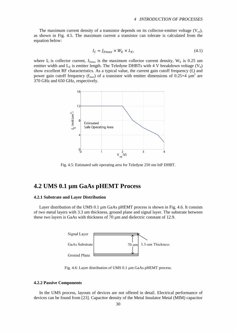
The maximum current density of a transistor depends on its collector-emitter voltage (Vce),
as shown in Fig. 4.5. The maximum current a transistor can tolerate is calculated from the
equation below:
, (4.1)
where IC is collector current, JEmax is the maximum collector current density, WE is 0.25 um
emitter width and LE is emitter length. The Teledyne DHBTs with 4 V breakdown voltage (Vb)
show excellent RF characteristics. As a typical value, the current gain cutoff frequency (ft) and
power gain cutoff frequency (fmax) of a transistor with emitter dimensions of 0.25×4 µm2 are
370 GHz and 650 GHz, respectively.
Fig. 4.5: Estimated safe operating area for Teledyne 250 nm InP DHBT.
4.2 UMS 0.1 µm GaAs pHEMT Process
4.2.1 Substrate and Layer Distribution
Layer distribution of the UMS 0.1 µm GaAs pHEMT process is shown in Fig. 4.6. It consists
of two metal layers with 3.3 um thickness, ground plane and signal layer. The substrate between
these two layers is GaAs with thickness of 70 µm and dielectric constant of 12.9.
Fig. 4.6: Layer distribution of UMS 0.1 µm GaAs pHEMT process.
4.2.2 Passive Components
In the UMS process, layouts of devices are not offered in detail. Electrical performance of
devices can be found from [23]. Capacitor density of the Metal Insulator Metal (MIM) capacitor
Page 39
4 INTRODUCTION OF PROCESSES
31
is 330 pF/mm2. Sheet resistances of Tantalum Nitride (TaN), Titanium Tungsten Silicon
(TiWSi) and GaAs resistors are 30, 1000 and 120 Ω/sq, respectively.
The transmission line loss in the UMS GaAs process is quite low. As a typical value, a 50 Ω,
quarter-wave transmission line at 100 GHz with 50 µm width and 250 µm length introduces
0.05 dB insertion loss.
4.2.3 Transistors
Minimum and maximum transistor dimensions in the UMS process are 100 µm × 125 µm
(two fingers and 20 µm gate width) and 105 µm × 230 µm (six fingers and 40 µm gate width),
respectively. The layouts of the two transistors are shown in Fig. 4.7. Maximum power density
of transistors based on this process is above 250 mW/mm, and the typical values of ft, fmax and
Vb are 130 GHz, 200 GHz and 6 V, respectively [23].
Fig. 4.7: Layouts of transistors with minimum and maximum sizes in UMS 0.1 µm GaAs pHEMT
process.
Page 40
4 INTRODUCTION OF PROCESSES
32
Page 41
33
Chapter 5
Power Amplifier Design in Teledyne
250 nm InP DHBT Process
In this chapter, the design of a power amplifier in the Teledyne 250 nm InP DHBT process is
explained in detail, which follows the design procedure described in Chapter 3. Selection of
devices, choice of optimum load and source impedances, comparison of power combining
networks and design of DC feed network are discussed in this chapter.
5.1 Single-Transistor Power Amplifier Design
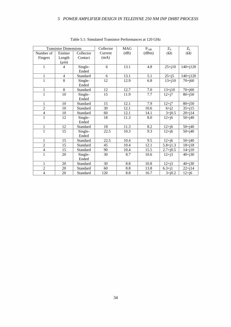
5.1.1 Device Selection
Improving power performance can be achieved by scaling up device size. However, this
comes at the cost of declined gain. Table 5.1 shows the maximum available gain (MAG) and
P1dB of transistors with different physical dimensions at 120 GHz with 2.5 V Vce bias. The
current density of each transistor is 6 mA/µm2, which is half of the maximum current density in
Fig. 4.5. P1dB of each transistor is extracted from load-pull and source-pull simulations by an
iterative method. With initial load and source impedances, a load-pull simulation is carried to
find the load impedance for optimum power performance. With this optimized load impedance,
a source-pull simulation is done to find the optimum source impedance. Following this, a load-
pull simulation is done again to find an optimum load impedance matching with the updated
source impedance. After several iterations, the optimum load and source impedances can be
achieved when the updated load/source impedance from load/source-pull simulation is the same
as the value from previous simulation.
As seen in Table 5.1, P1dB of a transistor is proportional to its finger number and emitter
length. However, the gain of a transistor declines with the increase of the emitter length. To
improve output power and keep sufficient gain, the four-finger transistor with 10 µm emitter
length is used in this thesis work. Theoretically, a four-finger, 15 µm emitter-length transistor is
available to achieve output power higher than that of a four-finger, 10 µm emitter-length
transistor. However, considering the lack of thermal model in the design kit and the current
compression from power dissipation in transistors with long fingers, the four-finger,
10 µm emitter-length transistor is applied in this design. In Fig. 5.1, measured and simulated I-V
curves of four-finger transistors with 10 µm and 20 µm emitter lengths are plotted for
comparison. It indicates that current compression is more severe in the transistor with longer
emitter length, but the device models don’t include this effect.
Page 42
5 POWER AMPLIFIER DESIGN IN TELEDYNE 250 NM INP DHBT PROCESS
34
Table 5.1: Simulated Transistor Performances at 120 GHz
Transistor Dimensions Collector
Current
(mA)
MAG
(dB)
P1dB
(dBm)
ZS
(Ω)
ZL
(Ω) Number of
Fingers
Emitter
Length
(µm)
Collector
Contact
1 4 Single-
Ended
6 13.1 4.8 25+j10 140+j120
1 4 Standard 6 13.1 5.1 25+j5 140+j120
1 8 Single-
Ended
12 12.9 6.8 13+j10 70+j60
1 8 Standard 12 12.7 7.0 13+j10 70+j60
1 10 Single-
Ended
15 11.9 7.7 12+j7 80+j50
1 10 Standard 15 12.1 7.9 12+j7 80+j50
2 10 Standard 30 12.1 10.6 6+j2 35+j15
4 10 Standard 60 12.1 14.1 3+j0.5 20+j14
1 12 Single-
Ended
18 11.3 8.0 12+j6 50+j40
1 12 Standard 18 11.3 8.2 12+j6 50+j40
1 15 Single-
Ended
22.5 10.3 9.3 12+j6 50+j40
1 15 Standard 22.5 10.4 9.5 12+j6 50+j40
2 15 Standard 45 10.4 12.1 5.8+j1.3 18+j18
4 15 Standard 90 10.4 15.5 2.7+j0.5 14+j10
1 20 Single-
Ended
30 8.7 10.6 12+j3 40+j30
1 20 Standard 30 8.8 10.8 12+j3 40+j30
2 20 Standard 60 8.8 13.8 6.3+j1 22+j14
4 20 Standard 120 8.8 16.7 3+j0.2 12+j6
Page 43
5 POWER AMPLIFIER DESIGN IN TELEDYNE 250 NM INP DHBT PROCESS
35
(a)
(b)
(c)
(d)
Fig. 5.1: (a) Measured I-V curve of a four-finger, 10 µm emitter-length transistor. (b) Measured I-V curve
of a four-finger, 20 µm emitter-length transistor. (c) Simulated I-V curve of a four-finger, 10 µm
emitter-length transistor. (d) Simulated I-V curve of a four-finger, 20 µm emitter-length transistor.
5.1.2 Choice of Bias Point
Class A and AB power amplifiers are suitable in this design. They have sufficient gain to
avoid severe P1dB compression from previous stage as explained in Section 3.1.2. Class AB is
preferred as its efficiency is higher than that of class A. The finally realized amplifier with class
AB biasing has gain of 6 dB at each stage. This value is lower than 12 dB MAG because of the
insertion loss of matching network and the bias point. The transistors are biased to Ibb = 1.5 mA,
Vce = 2.5 V and Icc = 42 mA. It can be estimated that Icc_max of a four-finger transistor with
10 µm emitter length is 120 mA from Eq. 4.1, and the quiescent current Icc is lower than half of
Icc_max.
5.1.3 In-Band Stability
Before finding the optimum source and load impedances, stability of the transistor is
checked. The selected Teledyne transistor biased at Ibb = 1.5 mA, Vce = 2.5 V and Icc = 42 mA is
unconditionally stable above 100 GHz, as seen from Fig. 5.2a. Stability factor and stability
Page 44
5 POWER AMPLIFIER DESIGN IN TELEDYNE 250 NM INP DHBT PROCESS
36
measure of the four-finger, 10 µm emitter-length transistor are above 1 and 0, respectively. The
schematic for stability simulations is shown in Fig. 5.2b.
(a) (b)
Fig. 5.2: (a) In-band stability factor and stability measure. (b) Schematic to test in-band stability.
5.1.4 Optimization of Load and Source Impedances
If a transistor is in-band unconditionally stable, it will not oscillate at the operating
frequencies with passive loads. The optimum load and source impedances are found by
load-pull and source-pull simulations at 120 GHz. Fig. 5.3a and 5.3b show the results of load-
and source-pull simulations at 120 GHz.
In this design, the optimum load impedance of the transistor is 16+j13 Ω. It is not the point
offering the highest P1dB but the point close to the center of PAE and Pdel contours. The value of
P1dB at this load impedance is relatively insensitive to variations of the load impedance. If the
load impedance is set at the point with maximum P1dB, a small error of output matching network
may shift the load impedance along the green arrow in Fig. 5.3c and therefore decrease P1dB
with slope steeper than other directions. Hence, to achieve a P1dB tolerating errors of output
matching network, the load impedance is set close to the center of PAE and Pdel. Based on this
point of view, the optimum source impedance is set to 5+j1 Ω.
Once the optimum load and source impedances are determined, the input power is swept to
analyze the power performance of the amplifier. In Fig. 5.4a, with increasing input power, the
ceiling of the load line moves close to the boundary of the safe operating area. Fig. 5.4b shows
Pout versus Pin and P1dB of the single-transistor power amplifier.
Page 45
5 POWER AMPLIFIER DESIGN IN TELEDYNE 250 NM INP DHBT PROCESS
37
(a)
(b)
(c)
Fig. 5.3: (a) Power-delivery (Pdel) contour and PAE contour of load-pull simulation. (b) Pdel contour and
PAE contour of source-pull simulation. (c) Pdel contour in load-pull simulation.
(a) (b)
Fig. 5.4: (a) Load-line of the single-transistor PA with different input power levels. (b) Pout versus Pin of
the single-transistor PA.
Page 46
5 POWER AMPLIFIER DESIGN IN TELEDYNE 250 NM INP DHBT PROCESS
38
5.2 Power Amplifier Topology
With known P1dB from a single-transistor PA, the number of amplifiers at the output stage
can be determined to estimate the system’s P1dB. In this design, a two-stage power amplifier
with 16 transistors in parallel at both the input and output stages is implemented. Without
consideration of losses from matching networks and gain compression from the first stage, a
P1dB of roughly 27 dBm is achieved. For power combination, a bus-bar combiner is used,
followed by matching networks to realize impedance conversion and current combining at each
node, as shown in Fig. 5.5.
Different types of power combining topologies are suitable in the Teledyne process. The
voltage combiner [24, 25] in Fig. 5.6a is a choice. The output impedance of this voltage
combiner is the sum of output impedances of each amplifier. However, it is difficult to combine
16 transistors through a voltage combiner and reported designs generally combine four
transistors. The other drawback of the voltage combiner is the asymmetry from parasitic
capacitors to ground. As shown in Fig. 5.6b, a real transformer is a transmission line with short
electrical length at the operating frequencies and therefore has distributed capacitors to ground.
Leakage current flowing to ground through the parasitic capacitors introduces phase and
amplitude imbalances among output ports of amplifiers [24]. Wilkinson power dividers, baluns
and directional couplers are not suitable either, they need several stages to combine 16
transistors.
Fig. 5.5: Schematic of the two-stage power amplifier based on bus-bar power combiner.
Page 47
5 POWER AMPLIFIER DESIGN IN TELEDYNE 250 NM INP DHBT PROCESS
39
(a) (b)
Fig. 5.6: (a) Schematic of a voltage combiner. (b) Model of voltage combiner with parasitic capacitors.
5.3 Matching Network Design
5.3.1 Output and Input Matching Networks
The complete power amplifier contains four identical sub-circuits in parallel. Matching
networks for the sub-circuits, which convert the complex conjugate of optimum load impedance
to 200 Ω, are analyzed. With four in parallel, the final output port of the whole amplifier is
matched to 50 Ω. Fig. 5.7a shows the schematic of the one-fourth output power combiner
realized by a two-stage, quarter-wave transformer for wideband considerations. Fig. 5.7b
illustrates Smith-chart representation of the matching network normalized to 200 Ω. With the
increasing of frequency, Zout of this one-fourth output network approaches to 200 Ω at 120 GHz.
Input matching network is designed in the same procedure. The one-fourth input matching
network is a two-stage, quarter-wave transformer and plotted in Fig. 5.7c with its Smith-chart
representation in Fig. 5.7d.
Page 48
5 POWER AMPLIFIER DESIGN IN TELEDYNE 250 NM INP DHBT PROCESS
40
(a)
(b)
(c) (d)
Fig. 5.7: (a) Schematic of one-fourth output matching network. (b) Smith-chart representation of the
one-fourth output matching network. (c) Schematic of one-fourth input matching network.
(d) Smith-chart representation of the one-fourth input matching network.
5.3.2 Interstage Matching Network
(a) Design of interstage matching network
As for the input and output matching networks, the interstage matching network has four
identical parts. Each part implements impedance matching between four transistors both at input
and output stages. Because ZL* = 16-j13 Ω and ZS
* = 5-j1 Ω, realizing interstage matching is
equivalent to make impedance matching between two low-impedance loads, as illustrated in
Fig. 5.8a. In order to improve the bandwidth of the interstage matching network, a low-high-low
impedance matching technology is used. Output and input impedances of the four-transistor
elements at the first and second stages are separately converted to high impedances around 40 Ω
at 120 GHz, and connected through a transmission line with 30 Ω characteristic impedance and
90° phase delay at 120 GHz. The schematic of the one-fourth interstage matching network is
plotted in Fig. 5.8b, and a test circuit shown in Fig. 5.9a verifies the frequency response. It is
Page 49
5 POWER AMPLIFIER DESIGN IN TELEDYNE 250 NM INP DHBT PROCESS
41
assumed that only common-mode signals propagate at input and output ports. The transmission
and reflection coefficients of the matching network are plotted in Fig. 5.9b.
(a) (b)
Fig. 5.8: (a) Interstage matching network. (b) Schematic of interstage matching network.
(a) (b)
Fig. 5.9: (a) Test circuit of intersage matching network. (b) S-parameters of the interstage matching
network.
(b) Analysis of wideband, low-high-low impedance conversion structure based on the
theory of small reflection
To explain the principle behind this impedance conversion structure, an analysis based on the
theory of small reflection is described below.
Fig. 5.10: Schematic of a low-high-low impedance conversion structure.
Page 50
5 POWER AMPLIFIER DESIGN IN TELEDYNE 250 NM INP DHBT PROCESS
42
From Fig. 5.10, reflection coefficients Г1, Г2, Г3 and Г4 at each interface can be written as
(5.1)
(5.2)
(5.3)
. (5.4)
The total reflection coefficient seen from Rs can be written as
(5.5)
(5.6)
, (5.7)
where ∆Ф is the phase difference from the center frequency. From Eq. 5.5, it can be seen that if
reflection coefficients of each stage are designed properly, the input reflection coefficient will
only have high-order components of ∆Ф, .i.e, (∆Ф2). Then Eq. 5.6 and 5.7 can be derived from
Eq. 5.5. Under these two assumptions, Гin is a weak function of ∆Ф during a wide frequency
range to achieve a wideband matching. For instance, if RS = 10 Ω, RL = 5 Ω, and the minimum
available characteristic impedance of the transmission line in the design is 15 Ω, ZT2 can be set
to 15 Ω and Г1 = -0.5. From Eq. 5.1-5.4, 5.6 and 5.7, ZH and ZT1 are 54.3 Ω and 25.3 Ω,
respectively.
To make a comparison between the new structure and a traditional matching network, a
traditional matching network with minimum characteristic impedance equal to 15 Ω is shown in
Fig. 5.11b. As seen in Fig. 5.11c, the transmission coefficient of the low-high-low impedance
conversion structure is flatter than that of the traditional matching network.
(a) (b) (c)
Fig. 5.11: (a) Schematic of a low-high-low impedance conversion network. (b) Schematic of a traditional
impedance matching network. (c) Transmission coefficients of the two networks.
The result of the low-high-low impedance conversion network in Figure 5.11 is similar to a
binomial transformer [22]. In order to increase the bandwidth, the characteristic impedances of
the transmission lines can be tuned to generate some ripples, and therefore the matching
network can be used as a Chebyshev transformer [22]. In Fig. 5.12a, a low-high-low impedance
matching network is implemented with ripples, and the transmission coefficient is plotted in
Fig. 5.12b with the result of the traditional matching network as a comparison. It indicates that
Page 51
5 POWER AMPLIFIER DESIGN IN TELEDYNE 250 NM INP DHBT PROCESS
43
the 0.5 dB bandwidth of the low-high-low impedance conversion network is roughly 100%
higher than that of a traditional matching network. In a practical design, source and load
impedances may have imaginary parts, which can be compensated by increasing or decreasing
the electrical lengths of the quarter-wave transformers.
(a) (b)
Fig. 5.12: (a) Schematic of the low-high-low impedance conversion network with ripples.
(b) Transmission coefficients of traditional matching network and the low-high-low impedance
conversion network with ripples.
5.3.3 In-Band Performances of the Sub-Circuit
In this section, in-band performances of the sub-circuit with input, interstage and output
matching networks are checked. It is to estimate the performances of the final design including
bias network, DC block and stabilizing resistors. In Fig. 5.13a, the sub-circuit is connected with
two 200 Ω terminals to measure its small signal gain and input and output reflection
coefficients. S-parameters and P1dB of this circuit are plotted in Fig. 5.13b and 5.13c,
respectively.
From data in Fig. 5.13, it can be estimated that the sub-circuit which parallels 4
transistors will achieve gain around 12.5 dB and P1dB approximate to 24.5 dBm. If the final
results of the complete PA with bias, DC feed and stabilizing network are not close to these
estimated results, the PA should be checked and optimized or even re-designed.
Page 52
5 POWER AMPLIFIER DESIGN IN TELEDYNE 250 NM INP DHBT PROCESS
44
(a)
(b) (c)
Fig. 5.13: (a) Test sub-circuit of the PA. (b) Small signal performances of the sub-circuit. (c) P1dB of the
sub-circuit.
5.4 Stabilizing and DC Feed Network Design
5.4.1 Out-of-Band Stabilization
To realize out-of-band stabilization, resistors are inserted into the matching networks,
specifically input of each stage for the consideration of efficiency. In this design, resistors are
inserted at the interface between two quarter-wave transmission lines, as shown in Fig. 5.14a.
These resistors realize out-of-band stabilization without strong gain reduction at the operating
frequencies. It is because the input impedances of the transistors increase after quarter-wave
transmission lines, and it reduces the effects of resistors in series. As shown in Fig. 5.14b,
stability factor improves significantly between 10-80 GHz with negligible effects around
110-140 GHz.
Page 53
5 POWER AMPLIFIER DESIGN IN TELEDYNE 250 NM INP DHBT PROCESS
45
(a) (b)
Fig. 5.14: (a) Sub-circuit with stabilizing resistors. (b) Stability factors of input stage after and before
inserting stabilizing resistors.
5.4.2 Cancellation of Odd-Mode Oscillation
In a power amplifier where several transistors are parallel combined, it is important to
remove the potential odd-mode oscillation [26]. The generation of odd-mode oscillation can be
explained briefly from Fig. 5.15a. In this circuit, it is assumed that input and output matching
networks (IMN and OMN) are lossless, and R1 and R2 are two resistors to stabilize the two
amplifiers operating at common mode. From the symmetry of the circuit, two virtual grounds
for odd-mode signals are generated at two nodes: one is between R1 and the IMN, and the other
is between R2 and the OMN. A simplified, odd-mode equivalent circuit is shown in Fig. 5.15b.
It is a circuit of two amplifiers with potential instability. To overcome this problem, two
resistors are inserted between the inputs and outputs of the two amplifiers, respectively. As
shown in Fig. 5.15c, these two resistors don’t attenuate common-mode signal gain, because
there are no voltage differences between the two input and output ports. To verify the validity of
the odd-mode stabilization, a test circuit in Fig. 5.15d shows the stability factor of the half
circuit with odd-mode stabilizing resistors. In this circuit, the amplifier is a four-finger, 10 µm
emitter-length transistor biased at Vce = 2.5 V and Icc = 42 mA. In Fig. 5.15e, stability factor and
stability measurement of circuits with and without odd-mode stabilizing resistors are compared,
and the potential instability is removed with two odd-mode stabilizing resistors.
Page 54
5 POWER AMPLIFIER DESIGN IN TELEDYNE 250 NM INP DHBT PROCESS
46
(a)
(b)
(c)
(d)
(e)
Fig. 5.15: (a) Potential odd-mode oscillation in a circuit with amplifiers in parallel. (b) A simplified
odd-mode equivalent circuit. (c) Circuit with odd-mode stabilizing resistors. (d) The half circuit for
measuring odd-mode stabilization. (e) Stability factor and stability measure for the half circuit with and
without odd-mode stabilizing resistors.
5.4.3 DC Feed Network
After the implementation of the RF chain, DC feed network should be designed with
negligible effects on RF chain at the operating frequencies. The topology of the DC feed
network used in this design is shown in Fig. 5.16a. At operating frequencies, the impedance at
the node connected to DC source is low due to the capacitor shorted to ground. Hence, through
a quarter-wave transformer, the output impedance of the DC feed network seen at the node
connected to the RF chain shows a high value to reduce its effect on the RF chain at operating
frequencies. The DC feed network is then connected to a node close to transistors in RF
networks, as it can mitigate the effects of DC feed network. To explain it clearly, design of the
DC feed network at output stage is used as an example. As shown in Fig. 5.16b, an OMN is
used to convert a lower output impedance at transistor’s output to a higher impedance in order
to match the 50 Ω terminal. Z1 and Z2 represent output impedance of the amplifier and output
Page 55
5 POWER AMPLIFIER DESIGN IN TELEDYNE 250 NM INP DHBT PROCESS
47
impedance seen from output matching network, respectively. Because Z1 is much smaller than
Z2, the paralleling load from DC feed network has less effects on the RF chain when it is closer
to the output of the transistor. Typically, in this design, Z1 is 1-j0.8 Ω when parallel combining
16 transistors, and Z2 is close to 50 Ω.
(a) (b)
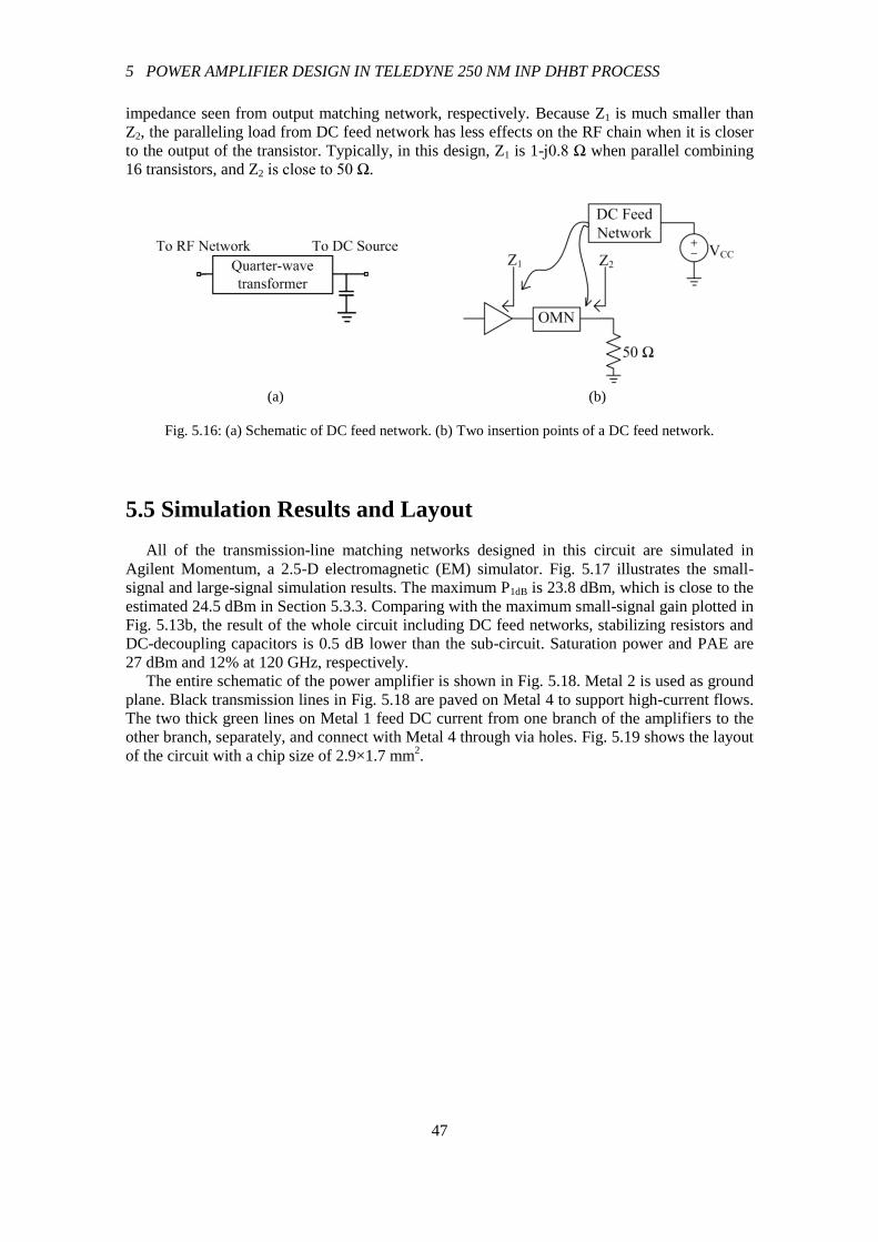
Fig. 5.16: (a) Schematic of DC feed network. (b) Two insertion points of a DC feed network.
5.5 Simulation Results and Layout
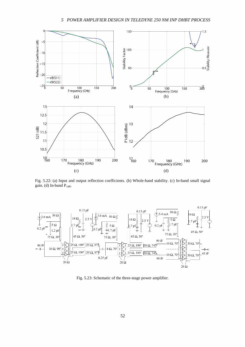
All of the transmission-line matching networks designed in this circuit are simulated in
Agilent Momentum, a 2.5-D electromagnetic (EM) simulator. Fig. 5.17 illustrates the small-
signal and large-signal simulation results. The maximum P1dB is 23.8 dBm, which is close to the
estimated 24.5 dBm in Section 5.3.3. Comparing with the maximum small-signal gain plotted in
Fig. 5.13b, the result of the whole circuit including DC feed networks, stabilizing resistors and
DC-decoupling capacitors is 0.5 dB lower than the sub-circuit. Saturation power and PAE are
27 dBm and 12% at 120 GHz, respectively.
The entire schematic of the power amplifier is shown in Fig. 5.18. Metal 2 is used as ground
plane. Black transmission lines in Fig. 5.18 are paved on Metal 4 to support high-current flows.
The two thick green lines on Metal 1 feed DC current from one branch of the amplifiers to the
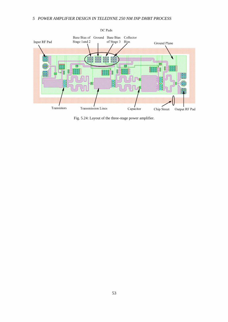
other branch, separately, and connect with Metal 4 through via holes. Fig. 5.19 shows the layout
of the circuit with a chip size of 2.9×1.7 mm2.
Page 56
5 POWER AMPLIFIER DESIGN IN TELEDYNE 250 NM INP DHBT PROCESS
48
(a)
(b)
(c)
(d)
(e)
Fig. 5.17: (a) Input and output reflection coefficients. (b) Whole-band stability factor. (c) In-band small
signal gain. (d) In-band P1dB. (e) Output power and PAE versus input power at 120 GHz.
Page 57
5 POWER AMPLIFIER DESIGN IN TELEDYNE 250 NM INP DHBT PROCESS
49
Fig. 5.18: Schematic of the power amplifier.
Fig. 5.19: Layout of the amplifier.
Page 58
5 POWER AMPLIFIER DESIGN IN TELEDYNE 250 NM INP DHBT PROCESS
50
5.6 Test Circuit Design for Tape-Out
In this section, a three-stage power amplifier operating at 180 GHz is presented. This power
amplifier uses two-finger, 10-µm emitter-length transistors for power amplification. Each
transistor is biased at Ibb = 0.9 mA, Vce = 2.5 V and Icc = 25 mA. The collector current is less
than half of Icc_max = 60 mA from Eq. 4.1. In the power amplifier, four transistors are paralleled
at the first stage and the second stage. Six transistors are combined at the output stage.
The two interstage matching networks are realized through low-high-low impedance conversion
structure. Performance of the power amplifier is shown in this section with electrical lengths of
all transmission lines defined at 180 GHz. All of the transmission-line matching networks are
simulated in Agilent Momentum, a 2.5-D electromagnetic (EM) simulator.
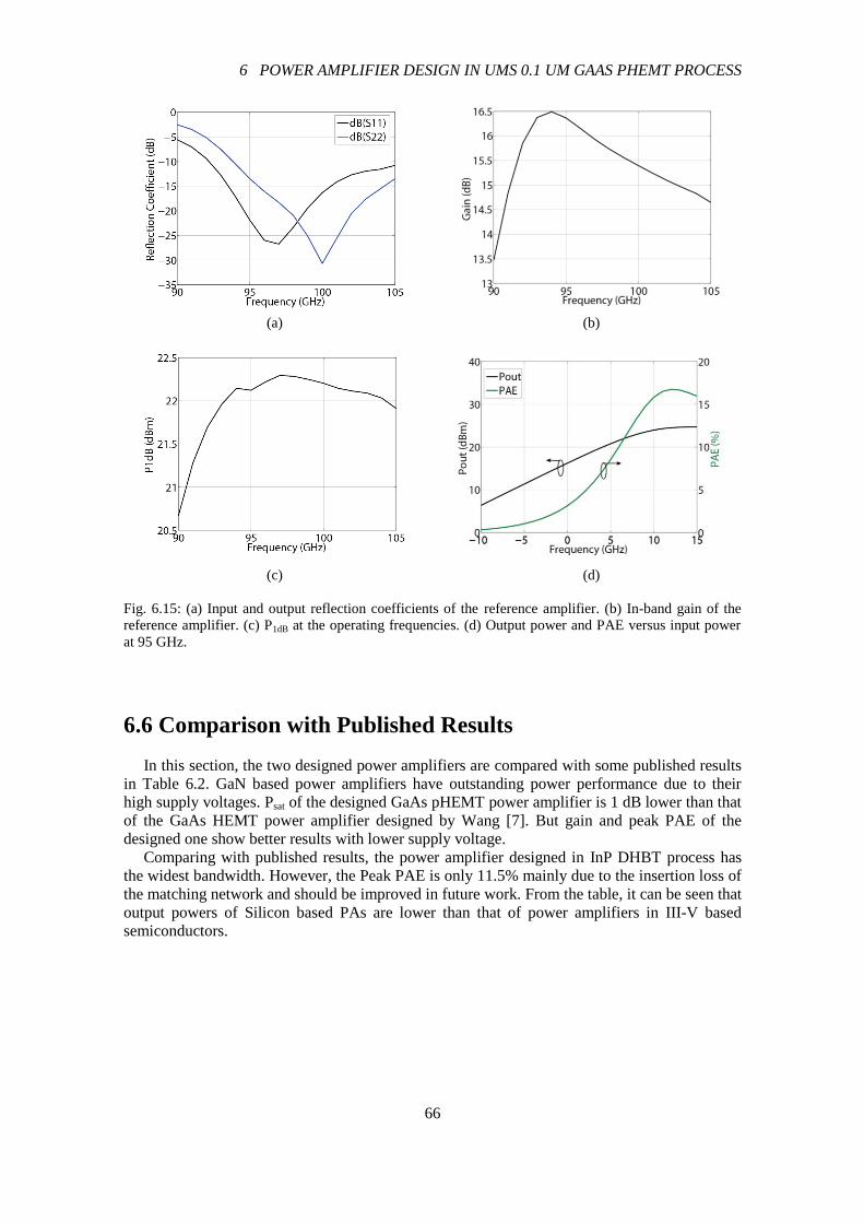
5.6.1 Performance of Matching Networks
The input and output matching networks are realized by two quarter-wave transmission lines.
The equivalent circuits and reflection coefficients of input and output matching networks are
shown in Fig. 5.20.
(a) (b)
(c) (d)
Fig. 5.20: (a) Schematic of input matching network. (b) Reflection coefficient of input matching network.
(c) Schematic of output matching network. (d) Reflection coefficient of output matching network.
The two interstage matching networks are realized through low-high-low impedance
conversion structure. The equivalent circuits and reflection coefficients of the two interstage
matching networks are shown in Fig. 5.21.
Page 59
5 POWER AMPLIFIER DESIGN IN TELEDYNE 250 NM INP DHBT PROCESS
51
(a)
(b)
(c) (d)
Fig. 5.21: (a) Schematic of interstage matching network between stage 1 and stage 2. (b) Reflection and
transmission coefficient between stage 1 and stage 2. (c) Schematic of interstage matching network
between stage 2 and stage 3. (d) Reflection and transmission coefficient between stage 2 and stage 3.
5.6.2 Performance and Layout
Fig. 5.22 illustrates the small-signal and large-signal simulation results. Small signal gain
and P1dB of this power amplifier are 12.5 dB and 13.5 dBm, respectively. The 3 dB bandwidth of
this power amplifier is above 40 GHz.
The schematic of the power amplifier is shown in Fig. 5.23. In this design, all transmission
lines are paved on Metal 4 with Metal 1 as ground plane. The layout of the power amplifier for
tape-out is shown in Fig. 5.24. The area of the chip including chip street is 2080 × 720 µm2.
Page 60
5 POWER AMPLIFIER DESIGN IN TELEDYNE 250 NM INP DHBT PROCESS
52
(a)
(b)
(c) (d)
Fig. 5.22: (a) Input and output reflection coefficients. (b) Whole-band stability. (c) In-band small signal
gain. (d) In-band P1dB.
Fig. 5.23: Schematic of the three-stage power amplifier.
Page 61
5 POWER AMPLIFIER DESIGN IN TELEDYNE 250 NM INP DHBT PROCESS
53
Fig. 5.24: Layout of the three-stage power amplifier.
Page 62
5 POWER AMPLIFIER DESIGN IN TELEDYNE 250 NM INP DHBT PROCESS
54
Page 63
55
Chapter 6
Power Amplifier Design in UMS
0.1 µm GaAs pHEMT Process
In this chapter, the design of a power amplifier in the UMS 0.1 µm GaAs pHEMT process is
carried out. Schematics and simulation results of combining and matching networks are
presented. To simplify the analysis, explanations of odd-mode oscillation and low-high-low
impedance matching network are not repeated in detail again.
6.1 Single-Transistor Power Amplifier Design
6.1.1 Device Selection
As the design procedure in Chap. 5, a single-transistor power amplifier is firstly designed
based on device selection, set of bias points and load/source impedance optimization. From
load- and source-pull simulations, small-signal power gain, P1dB and load/source impedances of
different transistors are listed in Table 6.1. In the simulation, under the bias of Vgs = 0.1 V and
Vds = 3 V, the transistors work as a 100 GHz class A power amplifier. It can be found in Fig. 6.1
that enlarging the transistor size is with the increasing of P1dB at the cost of gain reduction.
Another conclusion from Fig. 6.1 is that gain depends more on gate width rather than finger
number. In this design, the six-finger, 40 µm gate-width transistor is used with a three-stage
structure to compensate the low gain of the transistor.
Table 6.1: Load- and source-pull simulation results of transistors at 100 GHz
Size Gain (dB) P1dB (dBm) ZS (Ω) ZL (Ω)
2 × 20 µm 7.5 8.0 10+j7 16+j27
2 × 30 µm 6.4 10.5 5.5-j3 12+j16
2 × 40 µm 5.8 13.0 7.6-j7 15+j10
4 × 20 µm 6.8 12.0 5.3+j1 7.7+j13
4 × 30 µm 6.0 15.0 3.8-j4 7.3+j7.3
4 × 40 µm 5.4 16.5 3.0-j8 7.3+j7.5
6 × 20 µm 6.6 15.0 3.2-j0.8 7.3+j7.5
6 × 30 µm 5.9 17.0 3.6-j4.7 7.2+j2.4
6 × 40 µm 5.3 18.0 3.0-j5.5 7.3+j2.5
Page 64
6 POWER AMPLIFIER DESIGN IN UMS 0.1 UM GAAS PHEMT PROCESS
56
Fig. 6.1: P1dB and gain of transistors with different dimensions.
6.1.2 DC Bias Point Set and In-Band Stability
To achieve sufficient gain, the six-finger transistor with 40 µm gate width is biased to a
class A operating point with Vgs = 0.1 V and Vds = 3 V. As shown in Fig. 6.2a, drain current at
that gate bias is half of the maximum current, and the 3 V drain bias is between the knee voltage
(Vds = 1V) and the break-down voltage (Vds = 5V). In-band stability factor and stability measure
of the transistor is plotted in Fig. 6.2b, and the transistor is unconditionally stable from 80 GHz
to 120 GHz.
(a) (b)
Fig. 6.2: (a) I-V curves for the transistor with six fingers and 40 µm gate width. (b) In-band stability
factor and stability measure for the transistor biased to class A operating point.
6.1.3 Optimization of Load and Source Impedances
With a specific operating point, load- and source-pull simulations are done iteratively to find
optimum load and source impedances. Fig. 6.3 shows load- and source-pull simulation results.
The optimum load and source impedances are 6 Ω and 3-j5 Ω, respectively. As seen from the
Smith charts in Fig. 6.3, these two points are insensitive to variations of the load and source
impedances.
Page 65
6 POWER AMPLIFIER DESIGN IN UMS 0.1 UM GAAS PHEMT PROCESS
57
(a) (b)
Fig. 6.3: (a) Pdel and PAE contours of load-pull simulation. (b) Pdel and PAE contours of source-pull
simulation.
Fig. 6.4a shows the load line of the transistor with the optimum load and source impedances.
The purple dot in the figure is the bias point. Red lines with different current swings represent
load lines of different input power levels. Fig. 6.4b plots large signal parameters. PAE of the
single-transistor PA at 18 dBm P1dB is 19%.
(a) (b)
Fig. 6.4: (a) Load line of different input power levels. (b) Simulation results of large-signal parameters at
100 GHz.
6.2 Power Amplifier Topology
In this design, a 1-2-4 topology is used as shown in Fig. 6.5. Four transistors with 18 dBm
P1dB at output stage can achieve 24 dBm P1dB without the consideration of loss in matching
networks and gain compression from previous stages. Comparing with this 1-2-4 topology, a
1-1-4 topology is not suitable because the second stage will touch its P1dB prior to the output
stage. The 2-4-4 topology is an available choice, which improves the system P1dB but reduces
the PAE.
Page 66
6 POWER AMPLIFIER DESIGN IN UMS 0.1 UM GAAS PHEMT PROCESS
58
Fig. 6.5: A 1-2-4 power amplifier topology.
6.3 Matching Network Design
This section explains the design of the matching networks in the UMS process. To observe
the phase and amplitude imbalances from DC feed networks, simulations of all matching
networks include DC bias networks which stabilize the transistors from DC to operating
frequencies. The electrical lengths of all transmission lines in this design are defined at
100 GHz.
6.3.1 Input Matching Network
The input impedance of the first stage is converted to 50 Ω. It is realized by a transmission
line, as shown in Fig. 6.6a. The 12 Ω, 64° transmission line is for impedance conversion and the
50 Ω, 90° coupler line is aimed for DC blocking. Fig. 6.6b shows reflection coefficient at port 1.
(a) (b)
Fig. 6.6: (a) Schematic of input stage matching network. (b) Reflection coefficient at input stage.
6.3.2 Output Matching Network
To reduce chip area and insertion loss of matching networks, a planar spatial power
combiner is designed as an output matching network. The drawback of this structure is its
asymmetry, which generates odd-mode signal between two neighboring ports. Hence,
optimization is needed to minimize phase and amplitude imbalances at the four output ports.
After optimization, the maximum amplitude imbalance of the structure is 2.5 dB with a
maximum phase difference of 10°, as shown in Fig. 6.7.
Page 67
6 POWER AMPLIFIER DESIGN IN UMS 0.1 UM GAAS PHEMT PROCESS
59
(a) (b)
(c)
(d)
Fig. 6.7: (a) Schematic of asymmetric planar spatial power combiner. (b) Reflection coefficient at port 1.
(c) Transmission coefficients from port 1 to ports 2-5. (d) Phase delays from port 1 to ports 2-5.
(a) (b)
(c)
(d)
Fig. 6.8: (a) Schematic of symmetric planar spatial power combiner. (b) Reflection coefficient at port 1.
(c) Transmission coefficients from port 1 to ports 2-5. (d) Phase delays from port 1 to ports 2-5.
Page 68
6 POWER AMPLIFIER DESIGN IN UMS 0.1 UM GAAS PHEMT PROCESS
60
To prove that the performance degradation from these imbalances is acceptable, the other
symmetric power combiner is designed for comparison. Simulation results of these two
combiners are shown in Fig. 6.7 and 6.8. The insertion loss of the symmetric power combiner is
higher than the asymmetric one because of the longer physical length. Phase imbalance of the
symmetric combiner is 3° with amplitude imbalance less than 1dB.
In Fig. 6.9a and 6.9c, two combiners are connected “back-to-back”. Resistors are added
between neighboring ports to absorb differential signals. Comparing Fig. 6.9b and 6.9d, it can
be seen that the asymmetric power combiner can offer bandwidth over 12 GHz with insertion
loss less than 1 dB, and the insertion loss of the symmetric power combiner is over 1 dB with a
flat transmission coefficient over 20 GHz.
(a)
(b)
(c) (d)
Fig. 6.9: (a) Schematic of asymmetric combiners in “back-to-back” connection. (b) S-parameters of
asymmetric combiners in “back-to-back” connection. (c) Schematic of symmetric combiners in
“back-to-back” connection. (d) S-parameters of symmetric combiners in “back-to-back” connection.
6.3.3 Interstage Matching Network
To realize a wideband interstage matching, a low-high-low impedance conversion structure
is applied. In the design of interstage matching between stage 1 and stage 2, output impedance
of the first stage and input impedance of the second stage are converted to 60 Ω, and connected
by a 40 Ω, 90° coupler line, as shown in Fig. 6.10a. The S-parameters of the interstage matching
network are plotted in Fig. 6.10b and 6.10c. From 90 to 110 GHz, the reflection coefficient of
Page 69
6 POWER AMPLIFIER DESIGN IN UMS 0.1 UM GAAS PHEMT PROCESS
61
this matching network is lower than -10 dB, and the maximum amplitude imbalance between
ports 2 and 3 is less than 1.5 dB.
The matching network between stages 2 and 3 is plotted in Fig. 6.11a. The planar spatial
power combiner at the input of stage 3 incorporates power combining and matching network.
To test the amplitude and phase imbalances of the four ports at the input of stage 3, two output
nodes at stage 2 are shorted and excited by one terminal. S-parameters of the test circuit are
plotted in Fig. 6.11b and 6.11c. The maximum amplitude imbalance is 2.5 dB with maximum
phase difference of 15°.
(a)
(b) (c)
Fig. 6.10: (a) Schematic of interstage matching between stages 1 and 2. (b) Reflection and transmission
coefficients of matching network between stage 1 and 2. (c) Phase delays from port 1 to ports 2 and 3.
Page 70
6 POWER AMPLIFIER DESIGN IN UMS 0.1 UM GAAS PHEMT PROCESS
62
(a)
(b) (c)
Fig. 6.11: (a) Schematic of interstsage matching between stages 2 and 3. (b) Reflection and transmission
coefficients of matching network between stages 2 and 3. (c) Phase delays from stage 2 to four ports at
the input of stage 3.
6.4 Layout and Simulation Results
Finally, a power amplifier is implemented by assembling power combining networks and
transistors at each stage. An asymmetric power combiner is used at the output stage because of
the compact size and preferable performance. Fig. 6.12 shows schematic and layout of the
complete power amplifier.
Small-signal and large-signal parameters of this power amplifier are shown in Fig. 6.13.
Peak gain of the amplifier is 14 dB at 95 GHz with the maximum P1dB of 21.2 dBm. 3 dB
bandwidth of the amplifier is 12 GHz. PAE at 95 GHz plotted in Fig. 6.13 has the maximum
value of 15% with saturation power of 24 dBm. Stability factor and stability measure in Fig.
6.13d indicate the power amplifier is unconditionally stable.
Page 71
6 POWER AMPLIFIER DESIGN IN UMS 0.1 UM GAAS PHEMT PROCESS
63
(a)
(b)
Fig. 6.12: (a) Schematic of the power amplifier designed in UMS 0.1 µm GaAs pHEMT process.
(b) Layout of the PA (2.5×1.6 mm2).
Page 72
6 POWER AMPLIFIER DESIGN IN UMS 0.1 UM GAAS PHEMT PROCESS
64
(a) (b)
(c) (d)
(e)
Fig. 6.13: (a) Input and output reflection coefficients of the power amplifier. (b) Stability factor and
stability measure of the power amplifier. (c) In-band small signal gain of the amplifier. (d) In-band P1dB of
the amplifier. (e) Output power and PAE versus input power at 95 GHz.
6.5 Comparison with a Reference Design
To test the performances of the amplifier such as gain, P1dB and bandwidth, a design based on
ideal transmission lines without losses is implemented as a comparison. Schematic of the ideal
design is shown in Fig. 6.14. The combiner and splitter at the output stage are simply four
Page 73
6 POWER AMPLIFIER DESIGN IN UMS 0.1 UM GAAS PHEMT PROCESS
65
transmission lines connected to one node, and DC feed networks are realized by simple RF
chokes. The reference design doesn’t have any phase or amplitude imbalances at the power
combing and splitting networks. The small- and large-signal parameters are plotted in Fig. 6.15.
Comparing data in Fig. 6.14 and 6.15, it can be seen that the maximum gain of the designed
PA is 2.5 dB lower than the reference design. The maximum P1dB of the designed PA is 1 dB
less than the reference design because of the loss from output matching network.
From Fig. 6.13e and 6.15d, peak PAE of the designed amplifier is 2% lower than the reference
design. The drawback of the designed amplifier is the 12 GHz bandwidth which needs to be
improved in future work. In Fig. 6.15b, the 3 dB bandwidth of the reference design is above
15 GHz.
Fig. 6.14: Power amplifier implemented by ideal transmission lines.
Page 74
6 POWER AMPLIFIER DESIGN IN UMS 0.1 UM GAAS PHEMT PROCESS
66
(a)
(b)
(c)
(d)
Fig. 6.15: (a) Input and output reflection coefficients of the reference amplifier. (b) In-band gain of the
reference amplifier. (c) P1dB at the operating frequencies. (d) Output power and PAE versus input power
at 95 GHz.
6.6 Comparison with Published Results
In this section, the two designed power amplifiers are compared with some published results
in Table 6.2. GaN based power amplifiers have outstanding power performance due to their
high supply voltages. Psat of the designed GaAs pHEMT power amplifier is 1 dB lower than that
of the GaAs HEMT power amplifier designed by Wang [7]. But gain and peak PAE of the
designed one show better results with lower supply voltage.
Comparing with published results, the power amplifier designed in InP DHBT process has
the widest bandwidth. However, the Peak PAE is only 11.5% mainly due to the insertion loss of
the matching network and should be improved in future work. From the table, it can be seen that
output powers of Silicon based PAs are lower than that of power amplifiers in III-V based
semiconductors.
Page 75
6 POWER AMPLIFIER DESIGN IN UMS 0.1 UM GAAS PHEMT PROCESS
67
Table 6.2: Published W-band power amplifiers
Process Center
Frequency
(GHz)
Bandwidth
(GHz)
Gain
(dB)
P1dB
(dBm)
Psat
(dBm)
Peak
PAE
(%)
Supply
Voltage
(V)
Number of
Transistors
at Output
Stage
CMOS65nm
[11]
109 16 14.1 11.6 14.8 9.4 1.2 4
CMOS65nm
[27]
93 27 12 12.5 14.8 8.7 1.2 2
SiGe HBT
0.13um [28]
90 - 10.6 18.8 19.6 15.4 2.3 1
SiGe HBT
0.13um [29]
78 10 18 12.5 17 6.4 1.8 2
GaAs HEMT
0.1um[7]
94 10 9 - 25 10 4 8
GaAs pHEMT
0.1um
(this work)
95 12 14 21.5 24 14.5 3 4
GaN HEMT
0.15um [30]
88 10 20 26.2 29.3 15 14 4
GaN HEMT
0.15um [9]
91 7 16 - 32 10 20 8
GaN HEMT
0.14um [10]
92 8 17.6 - 30 19.4 12 -
InP HEMT
0.15um [8]
90 14 12 - 26 20 2.5 8
InP DHBT
0.7um [31]
92 - 5 - 14 10 2.25 1
InP HEMT
0.25um [32]
92 15 14.3 - 18.6 18.2 2.5 1
InP DHBT
0.25 um
(this work)
115 30 12 23.8 27.5 11.5 2.5 16
Page 76
6 POWER AMPLIFIER DESIGN IN UMS 0.1 UM GAAS PHEMT PROCESS
68
Page 77
69
Chapter 7
Conclusions and Future Work
7.1 Conclusions
In this thesis, two MMIC power amplifiers operating in W-band are presented. One is
designed in the Teledyne 250 nm InP DHBT process, and the other is designed in the UMS
0.1 µm GaAs pHEMT process. Performance such as gain and P1dB is reasonable and close to the
estimated limitations of the devices.
A low-high-low impedance conversion network composed by three-section quarter-wave
transformer is analyzed. It improves the bandwidth of the interstage matching networks. Planar
spatial power splitter and combiner are designed with good simulation results.
The two-stage InP power amplifier designed in the thesis presents a 3 dB bandwidth of more
than 30 GHz from 100 to 130 GHz. The P1dB is over 23 dBm from 105 to 130 GHz by parallel
combining 16 transistors at the output stage.
The three-stage GaAs power amplifier has a peak P1dB of 21.3 dBm with the maximum gain
of 14 dB. The power combiner and splitter at the final stage are implemented by a 4:1 planar
spatial power combiner and a 1:4 planar spatial power splitter, respectively. The asymmetric
combiner and splitter limit the 3 dB bandwidth of the amplifier to 12 GHz but realize a compact
design.
7.2 Future Work
In the design of the GaAs power amplifier, the planar spatial power combiner should be
optimized to reduce phase and amplitude imbalances between the four ports. The structure of
the DC feed networks should be optimized to reduce the phase and amplitude imbalances
between two ports.
In the InP power amplifier, the loss of the interstage matching network is 3 dB. The original
structure should be optimized to reduce the insertion loss of the matching networks and keep the
broad bandwidth.
Transistor models with parasitic components have to be extracted precisely in future designs
to improve the linearity of the amplifier and check the intrinsic load-line of the transistor.
Thermal effects should be added into the model for power amplifier designs.
To get a precise EM-simulation result, models of passive components such as via holes and
capacitors have to be verified in a 3-D EM simulator such as Computer Simulation Technology
(CST). The whole passive matching networks should be run in other EM simulators to compare
with the results in ADS.
Page 78
7 CONCLUSIONS AND FUTURE WORK
70
Page 79
71
Acknowledgements
I would like to thank my examiner Herbert Zirath, who gave me the opportunity to make a
thesis work which I am interested in and had meetings frequently to give me enough
instructions. Thanks to Vedran Furtula who offers the measurement data of the Teledyne DHBTs.
Thanks to Oliver Silva, Morteza Abbasi, Bing Zhang, Szhau Lai, Rumen Kozhuharov,
Zhongxia Simon He and Ferndando Diaz Canales. Without your helps and instructions, I can’t
finish my thesis so efficiently. Thanks to Sebastian Seb Gustafsson and other classmates who
have given me a lot of instructions and showed me Swedish cultures during these two years.
Thanks to Christian Fager and other professors who have helped me and encouraged me in this
two years’ study.
Page 80
ACKNOWLEDGEMENTS
72
Page 81
73
References
[1] M. Lucente, C. Stallo, T. Rossi, S. Mukherjee, E. Cianca, M. Ruggieri, V. Dainelli,
“Analysis and Design of a Point-to-Point Radio-Link at W Band for Future Satellite
Telecommunication Experiments,” in 2011 IEEE Aerospace Conference, pp. 1-10, Mar.
2011.
[2] O. Malca, E. Danieli, S. Gabay, A. Zilberman, N. S. Kopeika, A. Schechter, A.
Abramovich, “High resolution remote sensing of particles and aerosols in the W-Band (92
– 100 GHz),” in 2011 IEEE International Conference on Microwaves, Communications,
Antennas and Electronics Systems (COMCAS), pp. 7-9, Nov. 2011.
[3] M. Lucente, A. Salomè, E. Limiti, M. Ferri, L. Fiorani, W. R. Saleh, C. Stallo, M. Ruggieri
and G. Codispoti, “PLATON: Satellite Remote Sensing and Telecommunication by using
Millimetre Waves,” in 2012 IEEE First AESS European Conference on Satellite
Telecommunications (ESTEL), pp. 1-6, 2012.
[4] D. Hadziabdic and V. Krozer, “Power Amplifier Technology at Microwave and
Millimeter-Wave Frequencies: an Overview,” in 2008 Microwave Conference (GeMIC),
pp. 1-8, 2008.
[5] P. Huang, T. Huang, H. Wang, E. W. Lin, Y. Shu, G. S. Dow, R. Lai, M. Biedenbender
and J. H. Elliott, “A 94-GHz 0.35-W Power Amplifier Module,” in IEEE Trans. Microw.
Theory Tech., vol. 45, no. 12, pp. 2418-2423, Dec. 1997.
[6] J. Wells, “Faster than fiber: The future of multi-G/s wireless,” in Microwave Magazine, vol.
10, no. 3, pp. 104-112, May 2009.
[7] V. Dyadyuk, J. Kendall, J. Pathikulangara, O. Sevimli, L. Stokes, “Improved spectral
efficiency for a multi-gigabit mm-wave communication system,” in Microwave
Conference, pp. 810-813, Oct. 2007.
[8] D. L. Ingram, Y. C. Chen, J. Kraus, B. Brunner, B. Allen, H. C. Yen, and K. F. Lau, “A
427 mW, 20% compact W-band InP HEMT MMIC power amplifier,” in 1999 IEEE Radio
Frequency Integrated Circuits (RFIC) Symposium, pp. 95-98, Jun. 1999.
[9] A. Brown, K. Brown, J. Chen, K. C. Hwang, N. Kolias, and R. Scott, “W-Band GaN
Power Amplifier MMICs,” in 2011 IEEE MTT-S International Microwave Symposium
Digest (MTT), pp. 1-4, Jun. 2011.
Page 82
REFERENCES
74
[10] M. Micovic, A. Kurdoghlian, A. Margomenos, D. F. Brown, K. Shinohara, S. Burnham, I.
Milosavljevic, R. Bowen, A. J. Williams, P. Hashimoto, R. Grabar, C. Butler, A. Schmitz,
P. J. Willadsen and D. H. Chow, “92–96 GHz GaN power amplifiers,” in 2012 IEEE MTT-
S International Microwave Symposium Digest (MTT), pp. 1-3, Jun. 2012.
[11] Q. J. Gu, Z. Xu, and M. F. Chang, “Two-Way Current-Combining W-Band Power
Amplifier in 65-nm CMOS,” in IEEE Trans. Microw. Theory Tech., vol. 60, no. 5, pp.
1365-1374, May 2012.
[12] A. Komijani, A. Hajimiri, “A Wideband 77-GHz, 17.5-dBm Fully Integrated Power
Amplifier in Silicon,” in IEEE Journal of Solid-State Circuits, vol. 41, no. 8, pp. 1749-
1756, Aug. 2006.
[13] M. N. Yoder, “Wide Bandgap Semiconductor Materials and Devices,” in IEEE Trans.
Electron Devices, vol. 43, no. 10, pp. 1633-1636, Oct. 1996.
[14] W. R. Deal, K. Leong, V. Radisic, S. Sarkozy, “Low Noise Amplification at 0.67 THz
Using 30 nm InP HEMTs,” in IEEE Microw. Wireless Compon. Lett., vol. 21, no. 7, pp.
368-370, Jul. 2011.
[15] J. D. Cressler, “SiGe HBT Technology: A New Contender for Si-Based RF and
Microwave Circuit Applications,” in IEEE Trans. Microw. Theory Tech., vol. 46, no. 5, pp.
572 - 589, May 1998.
[16] S. M. Sze, High-Speed Semiconductor Devices. Wiely, first ed., 1990.
[17] D. A. Neamen, Semiconductor Physics and Devices: Basic Principles. McGraw-Hill, third
ed., 2003.
[18] J. Singh, Semiconductor Devices: an Introduction. McGraw-Hill, first ed., 1994.
[19] S. C. Cripps, RF Power Amplifiers for Wireless Communications. Artech House, second
ed., 2006.
[20] D. M. Pozar, Microwave Engineering. Wiley, fourth ed., 2011.
[21] S. P. Marsh, D. K. Y. Lau, R. Sloan, L. E. Davis, “Design and analysis of an X-band
MMIC “bus-bar” power combiner,” in 1999 Symposium on High Performance Electron
Devices for Microwave and Optoelectronic Applications, pp. 164-169, Nov. 1999.
[22] L. Li, K. Wu, “Integrated planar spatial power combiner,” in IEEE Trans. Microw. Theory
Tech., vol. 54, no. 4, pp. 1470 - 1476, Jun. 2006.
[23] 21 UMS PH10 Technology. [Online]. Available: http://www.ums-
gaas.com/telechargement/UMS_Flyer_PH10_technology.pdf
Page 83
REFERENCES
75
[24] I. Aoki, S. D. Kee, D. B. Rutledge, and A. Hajimiri, “Fully integrated CMOS power
amplifier design using the distributed active-transformer architecture,” in IEEE Journal of
Solid-State Circuits, vol. 37, no. 3, pp. 371-383, Mar. 2002.
[25] U. R. Pfeiffer, D. Goren, “A 23-dBm 60-GHz Distributed Active Transformer in a Silicon
Process Technology,” in IEEE Trans. Microw. Theory Tech., vol. 55, no. 5, pp. 857 - 865,
May 2007.
[26] Lorene Samoska, Kun-You Lint, Huei Wang, Yun-Ho Chungt, Michael Austt, Sander
Weinreb and Douglas Dawson, “On the Stability of Millimeter-Wave Power Amplifiers,”
in 2002 IEEE MTT-S International Microwave Symposium Digest, vol. 1, pp. 429 - 432,
Jun. 2002.
[27] K.J. Tsai, J.L. Kuo, and H. Wang, “A W-band Power Amplifier in 65-nm CMOS with
27GHz Bandwidth and 14.8dBm Saturated Output Power,” in Radio Frequency Integrated
Circuits Symposium, pp. 69-72, Jun. 2012.
[28] Michael C. and Gabriel M.R., “A Wideband High-Efficiency 79–97 GHz SiGe Linear
Power Amplifier with ≫ 90 mW Output,” in Bipolar/BiCMOS Circuits and Technology
Meeting, pp. 69-72, Oct. 2008.
[29] N. Demirel, E. Kerhervé, R. Plana and D. Pache, “79GHz BiCMOS Single-Ended and
Differential Power Amplifiers,” in Proceedings of the 40th European Microwave
Conference, pp. 1690-1693, Sep. 2010.
[30] M. Micovic, A. Kurdoghlian, K. Shinohara, S. Burnham, I. Milosavljevic and M. Hu,
“W-band GaN MMIC with 842 mW output power at 88 GHz,” in Microwave Symposium
Digest (MTT), pp. 237-239, May 2010.
[31] V.K. Paidi, Z. Griffith and Y. Wei, “G-band (140-220 GHz) and W-band (75-110 GHz)
InP DHBT Medium Power Amplifiers,” in IEEE Trans. Microw. Theory Tech., vol. 53,
no. 2, February 2005.
[32] M.Yu, M. Matloubian and P. Petre, “W-band InP HEMT MMICs Using Finite-Ground
Coplanar Waveguide (FGCPW) Design,” in IEEE Journal of Solid-State Circuits, vol. 34,
no. 9, pp. 1212-1218, September 1999.