X-BAND RF SWITCH IMPLEMENTATION IN SUBSTRATE INTEGRATED WAVEGUIDE A THESIS SUBMITTED TO THE GRADUATE SCHOOL OF NATURAL AND APPLIED SCIENCES OF MIDDLE EAST TECHNICAL UNIVERSITY BY TUNCAY ERDÖL IN PARTIAL FULFILLMENT OF THE REQUIREMENTS FOR THE DEGREE OF DOCTOR OF PHILOSOPHY IN ELECTRICAL AND ELECTRONICS ENGINEERING SEPTEMBER 2012
Transcript
i
X-BAND RF SWITCH IMPLEMENTATION IN SUBSTRATE INTEGRATED WAVEGUIDE
A THESIS SUBMITTED TO
THE GRADUATE SCHOOL OF NATURAL AND APPLIED SCIENCES OF
MIDDLE EAST TECHNICAL UNIVERSITY
BY
TUNCAY ERDÖL
IN PARTIAL FULFILLMENT OF THE REQUIREMENTS FOR
THE DEGREE OF DOCTOR OF PHILOSOPHY IN
ELECTRICAL AND ELECTRONICS ENGINEERING
SEPTEMBER 2012
ii
Approval of the thesis:
X-BAND RF SWITCH IMPLEMENTATION IN SUBSTRATE INTEGRATED WAVEGUIDE
submitted by TUNCAY ERDÖL in partial fulfillment of the requirements for the degree of Doctor of Philosophy in Electrical and Electronics Engineering Department, Middle East Technical University by, Prof. Dr. Canan ÖZGEN _____________ Dean, Graduate School of Natural and Applied Sciences Prof. Dr. İsmet ERKMEN _____________ Head of Department, Electrical and Electronics Eng. Assoc. Prof. Dr. Şimşek DEMİR _____________ Supervisor, Electrical and Electronics Eng. Dept., METU Prof. Dr. Altunkan HIZAL _____________ Co-Supervisor, Electrical and Electronics E. Dpt., METU Examining Committee Members : Prof. Dr. Sencer KOÇ _____________ Electrical and Electronics Engineering Dept., METU Assoc. Prof. Dr. Şimşek DEMİR _____________ Electrical and Electronics Engineering Dept., METU Assoc. Prof. Dr. Lale ALATAN _____________ Electrical and Electronics Engineering Dept., METU Prof. Dr. Nevzat YILDIRIM _____________ Electrical and Electronics Engineering Dept., METU Assoc. Prof. Dr. Vakur B. ERTÜRK _____________ Electrical and Electronics Eng. Dept., Bilkent University Date: 12.09.2012
iii
I hereby declare that all information in this document has been obtained and presented in accordance with academic rules and ethical conduct. I also declare that, as required by these rules and conduct, I have fully cited and referenced all material and results that are not original to this work.
Name, Last name : Tuncay ERDÖL Signature :
iv
X-BAND RF SWITCH IMPLEMENTATION IN SUBSTRATE
INTEGRATED WAVEGUIDE
ERDÖL, Tuncay
Ph.D., Department of Electrical and Electronics Engineering
Supervisor: Assoc. Prof. Dr. Şimşek DEMİR
September 2012, 92 pages
An RF switch in substrate integrated waveguide (SIW) technology for
X-band is designed and demonstrated. Design is based on embedding
shunt pin diodes of the switch in an evanescent mode waveguide filter. At
reverse bias, pin diodes formed a part of filter's capacitances. Thus switch
also functions as a filter when it is in “on” state. At forward bias of diodes,
capacitances of the filter are short circuited to obtain a good isolation. The
same circuit structure is used to design a tunable filter and an RF power
limiter which also functions as a filter. Several RF functions usually used in
RF frontends (power limiting, filtering, switching) are combined in a single
circuit which helps miniaturization of the frontend. The circuit can be
produced with standard PCB and chip&wire technology. The circuits
developed have comparable performances with microstrip counterparts
and they are advantageous to use in microwave systems using SIW as the
basic transmission medium and need filtering functionality.
Keywords: Substrate Integrated Waveguide (SIW), RF Switch, RF Power
Limiter, Tunable Filter
ABSTRACT
v
TABAN MALZEMEYE BÜTÜNLEŞİK DALGA KILAVUZUNDA
X-BANT RF ANAHTAR UYGULAMASI ERDÖL, Tuncay
Doktora, Elektrik ve Elektronik Mühendisliği Bölümü
Tez Yöneticisi: Doç. Dr. Şimşek DEMİR
Eylül 2012, 92 sayfa
Taban malzemeye bütünleşik dalga kılavuzu (TMBDK) yapısı içinde X-bant
için bir RF anahtar tasarlanıp gösterilmiştir. Tasarım, anahtarın paralel pin
diyotlarının sönümlenen dalga kılavuzu filtre tasarımında kullanılmasına
dayanır. Ters beslemede bu diyotlar, filtrenin sığalarının bir kısmını
oluşturur. Böylece anahtar açıkken filtre görevi de görür. Doğru beslemede
ise filtrenin sığaları kısa devre edilerek iyi bir izolasyon elde edilir. Aynı
devre yapısı ayarlanabilir filtre tasarımında ve filtre görevi de gören RF güç
sınırlayıcı tasarımında kullanılmıştır. RF önkatlarda genellikle kullanılan
birkaç RF fonksiyon (güç sınırlama, filtreleme, anahtarlama) tek bir
devrede gerçekleştirilerek önkatın küçültülmesine katkı sağlanmıştır. Devre
standart baskı devre ve hibrid üretim tekniğiyle üretilebilmektedir. Devreler
mikroşerit eşlenikleriyle benzer performansa sahiptir ve temel iletim
teknolojisi olarak TMBDK'yı kullanan ve filtreleme gereği olan sistemlerde
kullanımı avantajlıdır.
Anahtar Kelimeler: taban malzemeye bütünleşik dalga kılavuzu (TMBDK),
RF anahtar
ÖZ
vi
To My Family
vii
I want to express my gratitude towards my family for their support
throughout this study.
I am grateful to Assoc. Prof. Dr. Şimşek DEMİR, Assoc. Prof. Dr. Lale
ALATAN, Assoc. Prof. Dr. Vakur B. ERTÜRK for providing valuable
suggestions, guidance and motivation for years.
I am also grateful to Prof. Dr. Nevzat YILDIRIM, Prof. Dr. Sencer KOÇ for
valuable recommendations about writing of this thesis.
I want to thank Dr. Mustafa AKKUL, Şebnem SAYGINER and Dr. Taylan
EKER for their support throughout the doctoral period.
Technical assistances of Ömer ÖÇAL, Murat SERTKAYA, Tülay CAN,
Murat MUTLUOL and Sedat PEHLİVAN during the implementation of the
circuits are gratefully acknowledged.
I want to express my special thanks to my colleagues Mustafa Barış DİNÇ,
Hasan Hüseyin KILIÇ, Keziban AKKAYA for their support during this study.
Finally I want to thank to ASELSAN Company for technical support during
this work.
ACKNOWLEDGMENTS
viii
ABSTRACT… ............................................................................................ iv
ÖZ…………… ............................................................................................. v
ACKNOWLEDGMENTS ............................................................................ vii
TABLE OF CONTENTS ............................................................................ viii
LIST OF TABLES ....................................................................................... xi
LIST OF FIGURES .................................................................................... xii
LIST OF ABBREVIATIONS ...................................................................... xvi
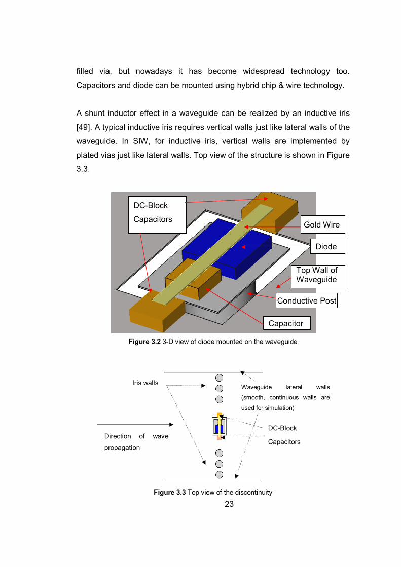
SIW RF power limiter will be demonstrated with two diodes for simplicity. In
the design of the limiter, two different diodes will be used which are
CLA4607 and CLA4604 of Skyworks Inc. CLA4607 diode has a thicker
intrinsic layer and thus higher compression point. It can handle higher
powers than CLA4604 which has a thinner intrinsic layer and lower
compression point. So the CLA4607 diode will be used at the second
resonator while at the last one CLA4604 will be used. The capacitor values
in the linear models of the diodes are used to design the proper
discontinuity which gives the necessary shunt inductance and capacitance
values. A ceramic SLC is also used with lumped capacitor to increase the
number of connections to the upper wall of the waveguide. Capacitance of
this ceramic SLC is taken into account and added to lumped capacitance.
Mounted diode and capacitors are shown in Figure 5.5. SIW power limiter
prototype is shown in Figure 5.4. Linear insertion loss measurement of the
limiter is shown in Figure 5.6.
58
Figure 5.4 Picture of SIW RF power limiter
Figure 5.5 Photo of CLA4604 diode and capacitors mounted together
Figure 5.6 Insertion loss of RF power limiter
Ceramic SLC
CLA4604
Diode
Lumped
Capacitor
59
In the nonlinear simulation of the structure, the parameters given in the
datasheets did not give very accurate results using the Robert-Caverly pin
diode model in AWR. So each diode’s nonlinear response (Pout vs. Pin) is
measured and diodes’ parameters in the simulator are optimized such that
simulation result is coincident with the measurement result. The measured
result for CLA4604 diode and its simulated result with optimized parameters
are shown in Figure 5.7. By the same way, the measured result for
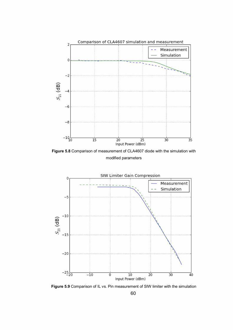
CLA4607 diode and its simulated result with optimized parameters are
shown in Figure 5.8. Using these parameters, SIW RF power limiter is
simulated. The simulation results are compared with the measurements
results in Figure 5.9 and Figure 5.10. Measurement is done at 8.5GHz. In
the prototyping, the same SIW PCB is used as the RF switch. Only the
diodes and capacitors differ from the switch. Additionally top of the diode
and capacitors are connected directly to the upper wall of the waveguide
and DC block capacitors are not used.
Figure 5.7 Comparison of measurement of CLA4604 diode with the simulation with
modified parameters
60
Figure 5.8 Comparison of measurement of CLA4607 diode with the simulation with
modified parameters
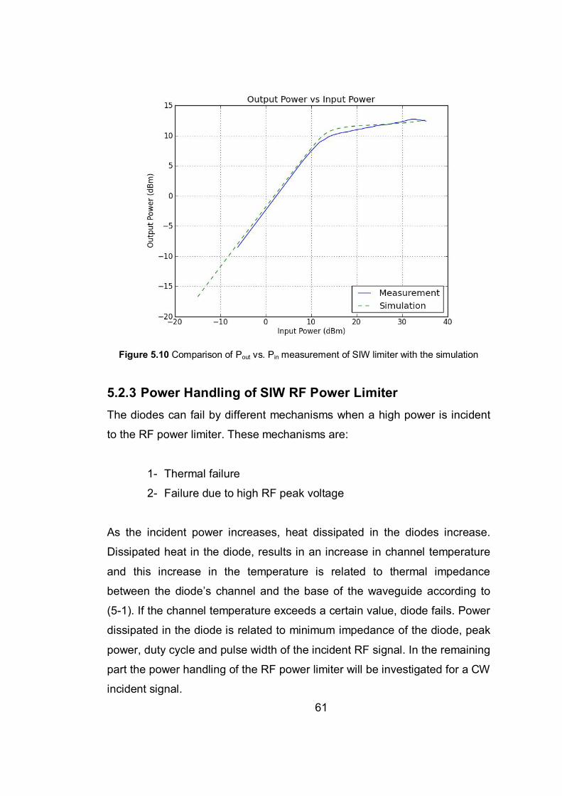
Figure 5.9 Comparison of IL vs. Pin measurement of SIW limiter with the simulation
61
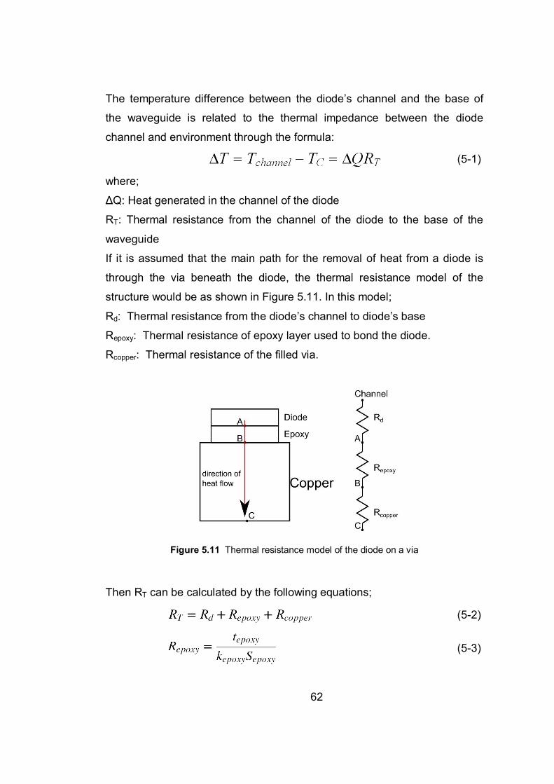
Figure 5.10 Comparison of Pout vs. Pin measurement of SIW limiter with the simulation
5.2.3 Power Handling of SIW RF Power Limiter The diodes can fail by different mechanisms when a high power is incident
to the RF power limiter. These mechanisms are:
1- Thermal failure
2- Failure due to high RF peak voltage
As the incident power increases, heat dissipated in the diodes increase.
Dissipated heat in the diode, results in an increase in channel temperature
and this increase in the temperature is related to thermal impedance
between the diode’s channel and the base of the waveguide according to
(5-1). If the channel temperature exceeds a certain value, diode fails. Power
dissipated in the diode is related to minimum impedance of the diode, peak
power, duty cycle and pulse width of the incident RF signal. In the remaining
part the power handling of the RF power limiter will be investigated for a CW
incident signal.
62
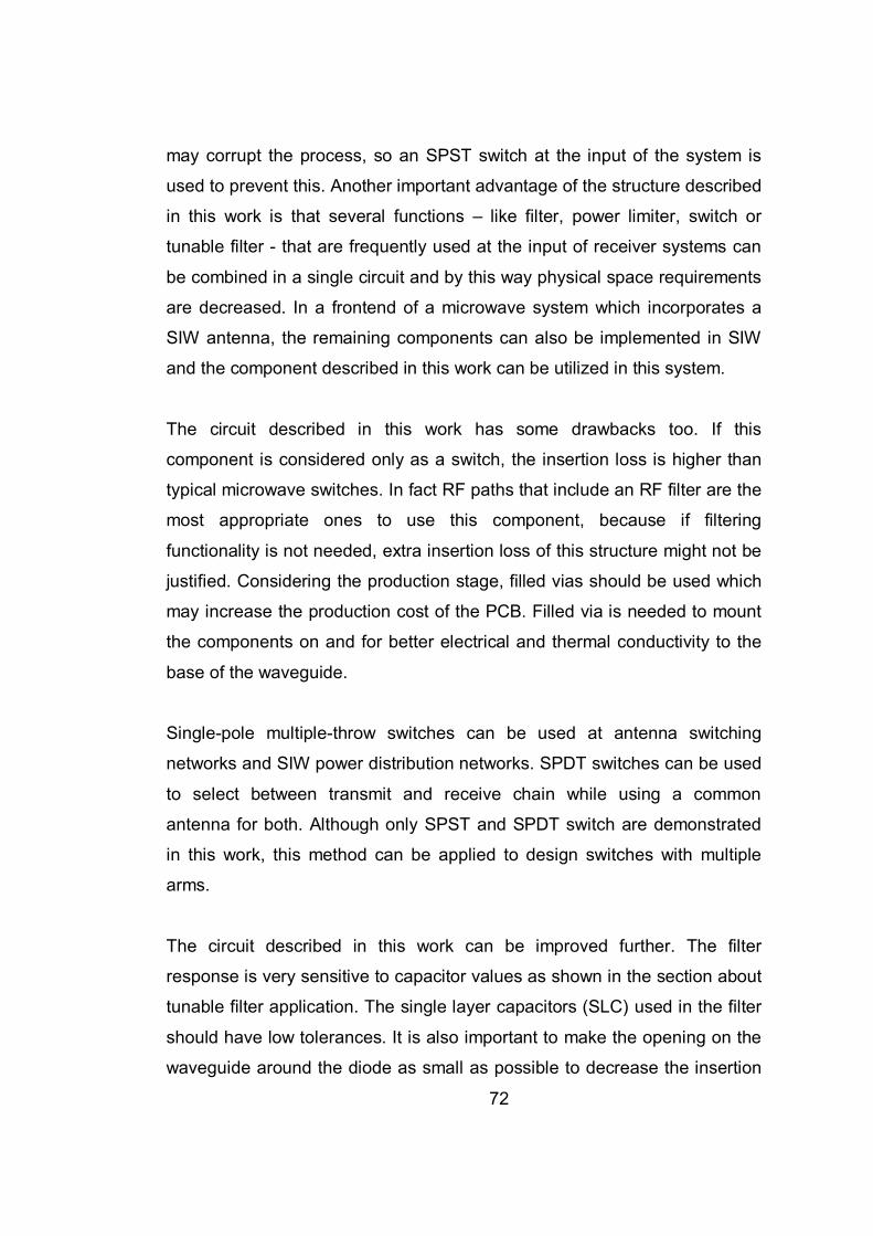
The temperature difference between the diode’s channel and the base of
the waveguide is related to the thermal impedance between the diode
channel and environment through the formula:
(5-1)
where;
ΔQ: Heat generated in the channel of the diode
RT: Thermal resistance from the channel of the diode to the base of the
waveguide
If it is assumed that the main path for the removal of heat from a diode is
through the via beneath the diode, the thermal resistance model of the
structure would be as shown in Figure 5.11. In this model;
Rd: Thermal resistance from the diode’s channel to diode’s base
Repoxy: Thermal resistance of epoxy layer used to bond the diode.
Rcopper: Thermal resistance of the filled via.
Figure 5.11 Thermal resistance model of the diode on a via
Then RT can be calculated by the following equations;
(5-2)
(5-3)
63
(5-4)
where;
tepoxy and tcopper are the thickness of epoxy layer and copper via.
kepoxy and kcopper are the thermal conductivities of epoxy and copper.
Sepoxy and Scopper are the surface area of epoxy layer and copper via.
Rd can be looked up from the datasheets and given in Table 5.1.
Table 5.1 Thermal resistances of the diodes
Diode Rd (oC/W)
CLA4607 40
CLA4604 100
Epoxy layer is in the shape of a square prism with 16mil side length and
1mil thickness (same as diode). Copper via is in cylindrical shape with
0.25mm radius and 0.5mm height. Maximum channel temperature for each
diode is 175oC and base of the waveguide is assumed to be at 85oC. Using
these data and thermal conductivity values for epoxy and copper, RT and
maximum allowable dissipated heat for each diode are calculated using
(5-1) thru (5-4) and given in Table 5.2.
Table 5.2 Thermal resistance of diodes and maximum allowed power dissipation on
diodes
Diode RT (oC/W) Maximum power dissipation (dBm)
CLA4607 48.5 32.7
CLA4604 108.5 29.2
64
Figure 5.12 Dissipated power in the diodes of SIW RF power limiter
Figure 5.13 Fundamental component of voltages across the diodes of SIW RF power
limiter
65
Dissipated powers in the diodes of SIW RF power limiter are given in Figure
5.12 with respect to input power. By inspecting this plot, if only the thermal
failure of diodes is considered, the power limiter can handle a maximum of
52dBm. Peak voltage levels on diodes are plotted in Figure 5.13. Only the
peak voltage associated with the fundamental component is plotted since
the other harmonics are much lower than the fundamental. CLA4604 can
handle 30V peak voltage and CLA4607 can handle 120V peak voltage. So,
according to Figure 5.13, failure due to peak voltage is a less stringent
failure mechanism than failure due to thermal breakdown. The same voltage
appears on the lumped capacitors too. For this reason, lumped capacitors
should be able to withstand the same voltage levels. Lumped capacitors
with 100V breakdown voltage are available and they can be used.
5.2.4 SIW RF Power Limiter/Switch For moderate power levels, this limiter structure can also be used as an RF
switch. Suppose that a SIW limiter is constructed by using CLA4607 diodes
at the first two resonators and CLA4604 diode at the last one. Consider a
single diode in this limiter as shown in Figure 5.14.
Figure 5.14 A representative single diode in limiter
If point P is shorted to ground, then this diode functions as a limiter. But if an
adequate current is injected to the diode by applying a suitable DC voltage
at this point, then diode becomes essentially short circuit and isolates the
input and output. So this structure can function both as a power limiter and
an RF switch if it is biased with a voltage source with low output impedance.
66
A voltage source with this property is an operational amplifier. This method
can work only for moderate RF power levels due to limited output current
capability of operational amplifiers, but voltage sources with higher current
capability can be designed and used by other means. In the simulations,
LM8261 Op-Amp [56] is used in buffer configuration (Figure 5.15). Spice
model of LM8261 is used for simulations. If 2V is applied to the Op-Amp,
then the diode becomes essentially short circuit. If 0V is applied to the Op-
Amp, then the diode behaves as an RF power limiter. Simulation results are
given in Figure 5.16, Figure 5.17 and Figure 5.18.
Figure 5.15 Single diode of RF switch biased with an Op-Amp
Figure 5.16 Response in isolation mode
67
Figure 5.17 Insertion loss and return loss of the switch for low power levels
Figure 5.18 Pin vs. Pout for SIW RF power limiter
68
5.3 Tunable Filter This structure can be used as a tunable filter to some degree. There are two
different capacitor values in a 3rd order filter (C1 and C2). The center
frequency of the filter can be changed by only varying these two capacitor
values. Although the shape of the filter is distorted a bit with varying center
frequency, the filter remains usable. The simulated response of the filter for
various values of capacitors is shown in Figure 5.19. C1 and C2 are found by
tuning for each center frequency. Variations of C1 and C2 values with
respect to center frequency are given in Figure 5.21. The difference
between C1 and C2 remains almost constant with varying center frequency.
This suggests that for moderate frequency tuning ranges, a 3rd order
tunable filter can be designed with a single type of varactor diode and center
frequency can be tuned with a single voltage. The variation of filter response
with respect to C1 while C2-C1 is constant (0.12pF) is plotted in Figure 5.20.
As shown in the plot, center frequency can be tuned over a frequency range
comparable to the filter’s bandwidth with single voltage without a significant
distortion in response.
Figure 5.19 Variation of the filter response while tuning
69
Figure 5.20 Variation of the filter response with single voltage tuning
Figure 5.21 The values C1 and C2 take with respect to center frequency
70
5.4 Conclusion
In this chapter two different applications of the same topology used in SIW
switch is given. The main difference between these circuits and the SIW RF
switch is the choice of diode types. In the RF power limiter application, pin
diodes with high power handling are chosen while varactor diodes are used
for tunable filter. Several RF functions can be combined in the same circuit
which enables integration of different capabilities in a smaller physical area.
RF power limiter and RF switch functions are combined in a single circuit as
an example. Varactor diodes and pin diodes can be used together to design
a switch with tunable center frequency. All the capacitors in the filter should
be tuned at the same time according to the center frequency of the filter to
tune the filter with low loss.
71
CHAPTER 6
CONCLUSIONS AND FUTURE STUDIES
In this thesis a design method for RF switches in a PCB using SIW structure
is described. This method enables incorporation of RF switches in substrate
integrated waveguide structures (slot arrays, power distribution circuits etc.).
The same circuit structure can also be used for other similar circuits
involving shunt diodes like tunable filter and RF power limiter. Several RF
functions can also be combined in a single circuit.
Although the RF components described in this thesis do not have any
particular performance advantages over similar RF components designed
for microstrip environment, they are more advantageous to use in SIW
environments. In a system which uses SIW as the basic transmission
medium, it is cumbersome to make transitions first to microstrip and then
back to SIW just to incorporate an RF switch in the path. These transitions
decrease the performance and increase physical space requirements.
At the front-ends of typical microwave receivers, several RF components
are present almost invariably. RF power limiters are used to protect
sensitive circuits from high power signals coming to the antenna. Pre-
selector filters are used to receive only the signals in the operating
frequency band and improve the spurious-free dynamic range of the
system. RF switches are also used at the input of systems to isolate the
signals coming from outside while measuring the noise level of the system.
Also during self-calibration and self-test of the system, incoming signals
72
may corrupt the process, so an SPST switch at the input of the system is
used to prevent this. Another important advantage of the structure described
in this work is that several functions – like filter, power limiter, switch or
tunable filter - that are frequently used at the input of receiver systems can
be combined in a single circuit and by this way physical space requirements
are decreased. In a frontend of a microwave system which incorporates a
SIW antenna, the remaining components can also be implemented in SIW
and the component described in this work can be utilized in this system.
The circuit described in this work has some drawbacks too. If this
component is considered only as a switch, the insertion loss is higher than
typical microwave switches. In fact RF paths that include an RF filter are the
most appropriate ones to use this component, because if filtering
functionality is not needed, extra insertion loss of this structure might not be
justified. Considering the production stage, filled vias should be used which
may increase the production cost of the PCB. Filled via is needed to mount
the components on and for better electrical and thermal conductivity to the
base of the waveguide.
Single-pole multiple-throw switches can be used at antenna switching
networks and SIW power distribution networks. SPDT switches can be used
to select between transmit and receive chain while using a common
antenna for both. Although only SPST and SPDT switch are demonstrated
in this work, this method can be applied to design switches with multiple
arms.
The circuit described in this work can be improved further. The filter
response is very sensitive to capacitor values as shown in the section about
tunable filter application. The single layer capacitors (SLC) used in the filter
should have low tolerances. It is also important to make the opening on the
waveguide around the diode as small as possible to decrease the insertion
73
loss. So a better solution for capacitors is to make a custom single layer
capacitor with tight tolerance and with a special geometry to cover the
opening as much as possible while at the same time allowing the mounting
of a diode. A tuning mechanism at the production stage can be useful. Two
kinds of tuning mechanism can be used:
1- Varactor diodes can be used for fine tuning of capacitance.
2- Custom built SLC capacitors can be designed in a special shape to
allow tuning with ribbon or bond wires at the testing stage of
production.
74
[1] Wu K., Deslandes D., Cassivi Y., “The Substrate Integrated Circuits - A New Concept for High-Frequency Electronics and Optoelectronics”, 6th International Conference on Telecommunications in Modern Satellite, Cable and Broadcasting Service, 2003. TELSIKS 2003. Volume 1, 1-3 Oct. 2003 Page(s): P - III-P-X vol.1. [2] Cassivi, Y., Perregrini, L., Arcioni, P., Bressan, M., Wu K., Conciauro, G., “Dispersion Characteristics of Substrate Integrated Rectangular Waveguide”, IEEE Microwave and Wireless Components Letters, Volume 12, Issue 9, Sep 2002 Page(s): 333 - 335. [3] Che W., Deng K., Wang D. and Chow Y.L., “Analytical equivalence between substrate-integrated waveguide and rectangular waveguide”, IET Microwaves, Antennas & Propagation, Volume 2, Issue 1, February 2008, Page(s):35 – 41. [4] Che W., Xu L., Wang D., Deng K., Chow Y.L., “Short-circuit equivalence between rectangular waveguides of regular sidewalls (rectangular waveguide and sidewalls of cylinders (substrate-integrated rectangular waveguides), plus its extension to cavity”, IET Microwaves, Antennas & Propagation, Volume 1, Issue 3, June 2007 Page(s):639 – 644. [5] Deslandes D., Wu K., “Integrated Microstrip and Rectangular Waveguide in planar form”, IEEE Microwave and Wireless Components Letters, Feb. 2001, Vol: 11, No: 2, Page(s):68-70. [6] Deslandes D., Wu K., “Integrated transition of coplanar to rectangular waveguides”, IEEE Microwave Symposium Digest, Volume 2, May 2001, Page(s):619 - 622. [7] Deslandes D., Wu K., “Design Consideration and Performance Analysis of Substrate Integrated Waveguide Components”, IEEE European Microwave Conference, Oct. 2002, Page(s):1 – 4. [8] Ding Y., Wu K., “Substrate Integrated Waveguide-to-Microstrip Transition in Multilayer Substrate”, IEEE Transactions on Microwave Theory and Techniques, Volume 55, Issue 12, Part 2, Dec. 2007 Page(s):2839 - 2844.
REFERENCES
75
[9] Suntives, A., Abhari, R., “Transition Structures for 3-D Integration of Substrate Integrated Waveguide Interconnects”, IEEE Microwave and Wireless Components Letters, Volume 17, Issue 10, Oct. 2007, Page(s):697 - 699. [10] Xu F., Wu K., “Guided-Wave and Leakage Characteristics of Substrate Integrated Waveguide”, IEEE Transactions on Microwave Theory and Techniques, Volume 53, Issue 1, Jan. 2005, Page(s):66 - 73. [11] Zhang S. Z., Yu Z. Y., Li C., Deng J. H., “Electromagnetic Energy Leakage Characteristics of Substrate Integrated Waveguide”, Asia-Pacific Microwave Conference Proceedings, APMC 2005, Volume 2, Dec. 2005. [12] Hong W., Liu B., Wang Y., Lai Q., Tang H., Yin X. X., Dong Y. D., Zhang Y., Wu K., “Half Mode Substrate Integrated Waveguide: A New Guided Wave Structure for Microwave and Millimeter Wave Application”, Joint 31st International Conference on Infrared Millimeter Waves and 14th International Conference on Terahertz Electronics, IRMMW-THz, Sept. 2006, Page(s):219 – 219. [13] Che W., Geng L., Deng K., Chow, Y.L., “Analysis and Experiments of Compact Folded Substrate-Integrated Waveguide”, IEEE Transactions on Microwave Theory and Techniques, Volume 56, Issue 1, Jan. 2008, Page(s):88 – 93. [14] Germain S., Deslandes D., Wu K., “Development of substrate integrated waveguide power dividers”, IEEE Canadian Conference on Electrical and Computer Engineering, Volume 3, May 2003, Page(s):1921 - 1924. [15] Zhang Z.-Y., Wu K., “A Broadband Substrate Integrated Waveguide (SIW) Planar Balun”, IEEE Microwave and Wireless Components Letters, Volume 17, Issue 12, Dec. 2007, Page(s):843 - 84. [16] Liu B., Hong W., Zhang Y., Tang H. J., Yin X. X., Wu K., “Half Mode Substrate Integrated Waveguide 180o 3-dB Directional Couplers”, IEEE Transactions on Microwave Theory and Techniques, Volume 55, Issue 12, Part 1, Dec. 2007, Page(s):2586 - 2592. [17] Djerafi T., Wu K., “Super-Compact Substrate Integrated Waveguide Cruciform Directional Coupler”, IEEE Microwave and Wireless Components Letters, Volume 17, Issue 11, Nov. 2007, Page(s):757 - 759. [18] Liu B., Hong W., Wang Y.-Q., Lai Q.-H., Wu K., “Half Mode Substrate Integrated Waveguide (HMSIW) 3-dB Coupler”, IEEE Microwave
76
and Wireless Components Letters, Volume 17, Issue 1, Jan. 2007, Page(s):22 - 24. [19] Cheng Y., Hong W., Wu K., “Half Mode Substrate Integrated Waveguide (HMSIW) Directional Filter”, IEEE Microwave and Wireless Components Letters, Volume 17, Issue 7, July 2007, Page(s):504 - 506. [20] Wang Y., Hong W., Dong Y., Liu B., Tang H. J., Chen J., Yin X., Wu K., “Half Mode Substrate Integrated Waveguide (HMSIW) Bandpass Filter”, IEEE Microwave and Wireless Components Letters, Volume 17, Issue 4, April 2007, Page(s):265 – 267. [21] Stephens, D., Young, P.R., Robertson, I.D., “W-band substrate integrated waveguide slot antenna”, IEE Electronics Letters Volume 41, Issue 4, Feb. 2005, Page(s):165 - 167. [22] Hong W., Liu B., Luo G.Q., Lai Q.H., Xu J.F., Hao Z.C., He F.F., Yin X. X., “Integrated Microwave and Millimeter Wave Antennas Based on SIW and HMSIW Technology”, International Workshop on Antenna Technology: Small and Smart Antennas Metamaterials and Applications, IWAT '07, March 2007, Page(s):69 - 72. [23] Hong W., Xu J., Lai Q., Chen P., “Design and implementation of low sidelobe slot array antennas with full and half mode substrate integrated waveguide technology”, IEEE European Microwave Conference, Oct. 2007, Page(s):428 - 429. [24] Yang S., Suleiman, S.H., Fathy, A.E., “Low Profile Multi-Layer Slotted Substrate Integrated Waveguide (SIW) Array Antenna with Folded Feed Network for Mobile DBS Applications”, IEEE Antennas and Propagation International Symposium, June 2007, Page(s):473 - 476. [25] Yan L., Hong W., Hua G., Chen J., Wu K., Cui T. J., “Simulation and Experiment on SIW Slot Array Antennas”, IEEE Microwave and Wireless Components Letters, Volume 14, Issue 9, Sept. 2004 Page(s):446 - 448. [26] Hao Z. C., Hong W., Chen X. P., Chen J. X., Wu K., Cui T. J., “Multilayered Substrate Integrated Waveguide (MSIW) Elliptic Filter”, IEEE Microwave and Wireless Components Letters, Volume 15, Issue 2, Feb. 2005 Page(s):95 - 97. [27] Deslandes D., Wu K., “Single-Substrate Integration Technique of Planar Circuits and Waveguide Filters”, IEEE Transactions on Microwave Theory and Techniques, Volume 51, Issue 2, Part 1, Feb. 2003 Page(s):593 - 596.
77
[28] Chen X., Hong W., Hao Z., Wu K., “Substrate Integrated Waveguide Quasi-Elliptic Filter Using Extracted-Pole Technique”, Asia-Pacific Microwave Conference Proceedings, APMC 2005, Volume 1, Dec. 2005. [29] Zhang Y. L., Hong W., Wu K., Chen J. K., Tang H. J., “Novel Substrate Integrated Waveguide Cavity Filter With Defected Ground Structure”, IEEE Transactions on Microwave Theory and Techniques, Volume 53, Issue 4, Part 1, April 2005, Page(s):1280 - 1287. [30] Hao Z. C., Hong W., Chen J. X., Chen X. P., Wu K., “Compact Super-Wide Bandpass Substrate Integrated Waveguide (SIW) Filters”, IEEE Transactions on Microwave Theory and Techniques, Volume 53, Issue 9, Sept. 2005, Page(s):2968 - 2977. [31] Chen X. P., Wu K., “Substrate Integrated Waveguide Cross-Coupled Filter with Negative Coupling Structure”, IEEE Transactions on Microwave Theory and Techniques, Volume 56, Issue 1, Jan. 2008, Page(s):142 - 149. [32] Deslandes D., Wu K., “Millimeter-wave substrate integrated waveguide filters”, IEEE Canadian Conference on Electrical and Computer Engineering, Volume 3, May 2003, Page(s):1917 – 1920. [33] Grigoropoulos, N., Sanz-Izquierdo, B., Young, P.R., “Substrate Integrated Folded Waveguides (SIFW) and Filters”, IEEE Microwave and Wireless Components Letters, Volume 15, Issue 12, Dec. 2005, Page(s):829 - 831. [34] Armendariz M., “Tunable Substrate Integrated Waveguide Filters Implemented With Pin Diodes and RF MEMS Switches”, M. Sc. Thesis, Dec. 2010. [35] Deslandes D., Wu K., “High Isolation Substrate Integrated Waveguide Passive Front-End for Millimeter-Wave Systems”, IEEE Microwave Symposium Digest, June 2006, Page(s):982 - 985. [36] He F. F., Wu K., Hong W., Han L., Chen W., “A Low Phase-Noise VCO Using an Electronically Tunable Substrate Integrated Waveguide Resonator”, IEEE Transactions on Microwave Theory and Techniques, Volume 58, Issue 12, Dec. 2010, Page(s):3452 - 3458. [37] Sirci S., Martinez J.D., Taroncher M., Boria V.E., “Varactor-Loaded Continuously Tunable SIW Resonator for Reconfigurable Filter Design”, Proceedings of the 41st European Microwave Conference, Oct. 2011, Page(s):436 – 439.
78
[38] Senior D. E., Cheng X., Yoon Y.-K., “Electrically Tunable Evanescent Mode Half-Mode Substrate-Integrated-Waveguide Resonators”, IEEE Microwave and Wireless Components Letters, Mar. 2012, Vol: 22, No: 3, Page(s):123-125. [39] Zhong C., Xu J., Yu Z., Zhu Y., “Ka-Band Substrate Integrated Waveguide Gunn Oscillator”, IEEE Microwave and Wireless Components Letters, July 2008, Vol: 18, No: 7, Page(s):461-463. [40] Senior D.E., Cheng X., Yoon Y. K., “A Compact, Single-Layer Substrate Integrated Waveguide (SIW) Cavity-Backed Active Antenna Oscillator”, IEEE Antennas and Propagation Letters, 2012, Vol: 11, Page(s):431-433. [41] Abdolhamidi M., Shahabadi M., “X-Band Substrate Integrated Waveguide Amplifier”, IEEE Microwave and Wireless Components Letters, Dec. 2008, Vol: 18, No: 12, Page(s):815-817. [42] Zhang Z. Y., Wei Y. R., Wu K., “Broadband Millimeter-Wave Single Balanced Mixer and Its Applications to Substrate Integrated Wireless Systems”, IEEE Transactions on Microwave Theory and Techniques, Volume 60, Issue 3, Mar. 2012, Page(s):660 - 669. [43] Sbarra E., Marcaccioli L., Gatti R. V., Sorrentino R., “Ku-band analogue phase shifter in SIW technology”, Proceedings of the 39th European Microwave Conference, Sep. 2009, Page(s):264 – 267. [44] Ruo Feng Xu, B. Sanz Izquierdo, P. R. Young, “Switchable Substrate Integrated Waveguide”, IEEE Microwave and Wireless Components Letters, Apr. 2011, Vol: 21, No: 4, Page(s):194-197. [45] Ghiotto A., Adhikari S., Wu K., “Ferrite-Loaded Substrate Integrated Waveguide Switch”, IEEE Microwave and Wireless Components Letters, Mar. 2012, Vol: 22, No: 3, Page(s):120-122. [46] Farrall A. J., Young P. R., “Substrate Integrated Rectangular Waveguides”, IEEE High Frequency Postgraduate Student Colloquium, 2004. [47] GC4271 product page, 15.04.2012, http://www.microsemi.com/en/products/product-directory/77022, Last accessed on 17-08-2012. [48] Sickel T., “Tunable Evanescent Mode X-Band Waveguide Switch”, Ph. D. Thesis, Dec. 2005.
79
[49] Marcuvitz N., Waveguide Handbook (IEEE Electromagnetic Waves Series), 1986. [50] Microstrip Filters for RF/Microwave Applications. Jia-Sheng Hong, M. J. Lancaster, John Wiley & Sons, 2001. [51] Craven G. F., Mok C. K., “The Design of Evanescent Mode Waveguide Bandpass Filters for a Prescribed Insertion Loss Characteristic”, IEEE MTT, March 1971. [52] Engen G. F., Hoer C. A., “Thru-Reflect-Line, An Improved Technique for Calibrating the Dual Six-Port Automatic Network Analyzer”, MTT, December 1979. [53] ANSYS HFSS 3D EM Simulation software <www.ansys.com>, Last accessed on 26-08-2012. [54] Advanced Wave Research (AWR) Official Web Page, <www.awrcorp.com>, Last accessed on 26-08-2012. [55] RO4000 Series High Frequency Circuit Materials, Rogers Corp., http://www.rogerscorp.com/documents/726/acm/RO4000-Laminates---Data-sheet.aspx, Last accessed on 17-08-2012. [56] LM8261 datasheet, http://www.ti.com/product/lm8261, Last accessed on 19-08-2012. [57] DLI Di-Cap model parameters, http://www.dliextra.net/capcad/DiCaps.aspx, Last accessed on 26-08-2012. [58] “Establishing the Minimum Reverse Bias for a PIN Diode in a High-Power Switch”, Rev. V2, M/A-COM Technology Solutions application note, http://www.macomtech.com/Application%20Notes/pdf/AN3022.pdf, Last accessed on 26-08-2012. [59] Di-Cap, http://www.dilabs.com/pdfs/Pg%208-11%20SLC%20Di-Cap_02-2011.pdf, Last accessed on 26-08-2012.
80
APPENDIX A
EVANESCENT-MODE WAVEGUIDE FILTER DESIGN
In this part, the design of an evanescent mode waveguide filter will be
summarized. The design method begins with choosing a filter prototype.
Since the lumped element equivalent circuit of an admittance inverter is very
similar to the lumped element equivalent circuit of a waveguide section in
evanescent mode, band pass filter circuit formed by shunt L-C resonators
coupled by admittance inverters (J-inverters) is chosen as the starting point.
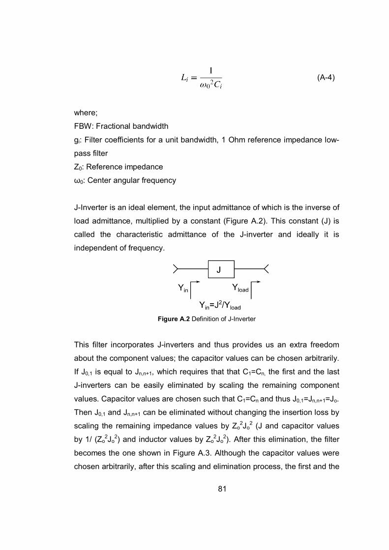
The circuit is shown in Figure A.1 [50]. Circuit parameters can be calculated
using equations (A-1) thru (A-4). In this derivation, it is assumed that
reference impedance of both ports are equal to each other (Zo).
Figure A.1 Filter formed by L-C resonators coupled by J-inverters
(A-1)
(A-2)
(A-3)
81
(A-4)
where;
FBW: Fractional bandwidth
gi: Filter coefficients for a unit bandwidth, 1 Ohm reference impedance low-
pass filter
Z0: Reference impedance
ω0: Center angular frequency
J-Inverter is an ideal element, the input admittance of which is the inverse of
load admittance, multiplied by a constant (Figure A.2). This constant (J) is
called the characteristic admittance of the J-inverter and ideally it is
independent of frequency.
Figure A.2 Definition of J-Inverter
This filter incorporates J-inverters and thus provides us an extra freedom
about the component values; the capacitor values can be chosen arbitrarily.
If J0,1 is equal to Jn,n+1, which requires that that C1=Cn, the first and the last
J-inverters can be easily eliminated by scaling the remaining component
values. Capacitor values are chosen such that C1=Cn and thus J0,1=Jn,n+1=Jo.
Then J0,1 and Jn,n+1 can be eliminated without changing the insertion loss by
scaling the remaining impedance values by Zo2Jo
2 (J and capacitor values
by 1/ (Zo2Jo
2) and inductor values by Zo2Jo
2). After this elimination, the filter
becomes the one shown in Figure A.3. Although the capacitor values were
chosen arbitrarily, after this scaling and elimination process, the first and the
82
last capacitors (C1’ and Cn’) become a certain value regardless of their initial
value.
Figure A.3 J-Inverter coupled band pass filter circuit
(A-5)
(A-6)
(A-7)
gi can be calculated according to the chosen filter response shape. If the
main functionality of the circuit is RF switching and out-of-band response is
not important, then Butterworth response can be chosen which provides
maximally flat insertion loss response in the pass band of the filter. If the
filtering functionality is important too, then Chebyshev response can be
chosen which provides steepest skirts at the edges of the pass band for the
same degree of filter. gi values for Butterworth response can be calculated
using (A-8) and (A-9) and gi values for Chebyshev response can be
calculated using (A-9), (A-10), (A-11) and (A-12) [50].
(A-8)
(A-9)
83
(A-10)
(A-11)
(A-12)
where;
n: degree of the filter.
Rdb: ripple of insertion loss in dB
The input and output waveguides should allow propagation at the operating
frequency band. However, the cutoff frequency of the waveguide in which
the filter is built is above the operating frequency band and the wave is
evanescent. So there should be a waveguide discontinuity at both ends of
the filter. A EWG-WG junction can be modeled by a susceptance and a
transformer (Figure A.4) [49]. The n and Lp parameters of the equivalent
circuit are given in [49] for a symmetric hollow waveguide transition, but full-
wave simulation should be used to calculate the exact values for an
arbitrary waveguide transition.
Figure A.4 Equivalent circuit of waveguide transition
84
These junctions can be absorbed in filter design by scaling all impedance
values in the circuit by 1/n2 and modifying the first and last inductance
values. It is assumed that input and output waveguides of the filter are
identical. The resultant circuit is shown in Figure A.5. The circuit in Figure
A.5 should be functionally equivalent to the circuit in Figure A.3, so the
equations (A-13) and (A-14) should be satisfied.
Figure A.5 J-Inverter coupled band pass filter circuit with equivalent circuits of waveguide
junctions at both end.
(A-13)
(A-14)
The ABCD matrix of an ideal admittance inverter (J-inverter) is
(A-15)
The circuit equivalent of a J-inverter that will result in the same ABCD matrix
is shown in Figure A.6.
Figure A.6 J-Inverter circuit representation
85
Although the susceptances in this ideal circuit are frequency independent, at
a narrow frequency band they can be realized by positive and negative
valued inductances (Figure A.7). The characteristic admittance of the
inverter will be exact only at the mid-band frequency.
Figure A.7 Lumped equivalent of a J-Inverter
The equivalent circuit of a section of uniform waveguide in cutoff is given in
Figure A.8. The impedance values can be calculated by equations (A-16),
(A-17) and (A-18). The field in an evanescent mode waveguide decays
exponentially. The waveguide impedance is complex for the frequencies
below cutoff. The equivalent circuit can be considered as an attenuator
renormalized by complex characteristic impedance.
Figure A.8 Equivalent circuit of a waveguide in cutoff
(A-16)
(A-17)
86
(A-18)
where;
le: Length of the evanescent mode waveguide section
X0: Absolute value of the characteristic impedance of evanescent mode
waveguide section at frequencies below cut-off
γ: Absolute value of the propagation constant of the evanescent mode
waveguide section
b: Height of the evanescent mode waveguide section
a: Width of evanescent mode waveguide section
J-inverters in Figure A.3 can be replaced by an EWG section between two
shunt inductors. This transformation is shown in Figure A.9. The equations
about this transformation are given in (A-19), (A-20), (A-21) and (A-22). The
length of EWG section is calculated from J-inverter value by equations
(A-19) and (A-20) and shunt susceptances at input and output of EWG
section is calculated by (A-22).
Figure A.9 Equivalent circuit of a J-inverter and its equivalent one as a EWG section
between two shunt inductive impedances (Z3)
(A-19)
(A-20)
(A-21)
87
(A-22)
where X0, le and γ are impedance, length and absolute value of propagation
constant of the EWG section respectively. Note that parallel combination of
Z2 and Z3 is equal to -Z1.
After this transformation the filter circuit becomes the one shown in Figure
A.10. Equivalent shunt inductor values of Z3 impedances for each J-inverter
are calculated at center frequency of the filter. The final simplified circuit is
shown in Figure A.11. Equations (A-23) thru (A-28) should be used to
calculate the parameters of circuit elements.
Figure A.10 Evanescent mode filter with waveguide steps at both ends
(A-23)
(A-24)
(A-25)
Figure A.11 Evanescent mode filter with waveguide steps at both ends
88
(A-26)
(A-27)
(A-28)
Consider the transformation in Figure A.9 again. Z1 is determined by the
value of the J-inverter and it is related to the impedance (X0), propagation
constant (γ) and the length of the EWG section (le). Physically the
dimensions of the EWG and the design frequency determine the
characteristic admittance of the J-inverter. In general, the width, height,
dielectric material etc, are determined beforehand, and the frequency is
chosen to be the center frequency of the filter. Thus, X0 and γ is fixed and
length is calculated according to the characteristic admittance of a J-
inverter.
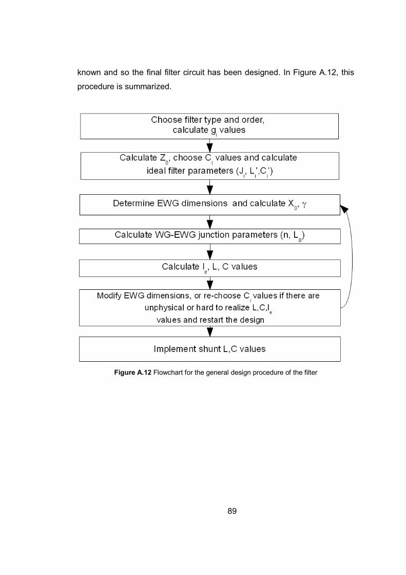
So after the determination of the ideal filter components (Figure A.3), the
dimensions of the EWG must be chosen. For SIW structure it is best to
choose the height the same as the input and output waveguides. So only
the width of the EWG is should be chosen such that the cutoff frequency of
the waveguide is higher than the maximum operating frequency of the filter.
The dimensions of the EWG and the center frequency determine the
impedance of the EWG (X0), the n and Lp of the junction. The component
values of the ideal filter would be manipulated according to n, Lp values to
absorb the junction in the filter design. At this point J-inverter characteristic
admittances are known and they should be used to calculate the lengths of
EWG sections. Then X0 and lengths of the EWG sections will be used to
calculate Z3 values in Figure A.9. These Z3 values and Lp values are used to
calculate new inductor values of the circuit. At this point equivalent
inductance, capacitance values and dimensions of EWG sections are
89
known and so the final filter circuit has been designed. In Figure A.12, this
procedure is summarized.
Figure A.12 Flowchart for the general design procedure of the filter
90
APPENDIX B
MATERIALS AND DEVICES USED AT THE DESIGN AND PROTOTYPES
In this part, the specifications of various devices and materials utilized in the
design and implementations will be summarized. The data shown are
mostly gathered from the official datasheets of the devices and the name of
the manufacturer can be referred as the reference of the data presented.
B.1. GC4271 Pin Diode GC4271 diode of Microsemi[47] is the pin diode used for prototyping the RF
switches. It comes with its own gold wires on it which makes it easier to use.
The drawing of the diode’s package is shown in Figure B.1 and the
properties of the diode are shown in Table B.1.
Figure B.1 The drawing of the pin diode used for the design and the fabrication of the
prototypes
Table B.1 Properties of GC4271
Model Number
Breakdown Voltage
Junction Capacitance
Series Resistance
Carrier Lifetime
Thermal Resistance
GC4271 70V 0.1pF 1.0 Ohm 100ns 70 oC/W
91
B.2. CLA4604 and CLA4607 Pin Diodes CLA4604 and CLA4607 are the two diodes used in the RF power limiter
circuit. CLA4607 is the first diode at the input of the limiter which has a
thicker I-region and higher RF power handling. CLA4604 is the second
diode with thinner I-region and lower RF leakage power. Properties of these
diodes are given in Table B.2.
Table B.2 Properties of CLA4604 and CLA4607
Model
Number
Breakdown
Voltage
Junction
Capacitance
Series
Resistance
I-Region
Thickness
Thermal
Impedance
For CW
Signals
CLA4604 30V 0.12pF 2.5 Ohm 2 µm 100 oC/W
CLA4607 120V 0.20pF 2.0 Ohm 7 µm 40 oC/W
B.3. RO4003 Substrate Material RO4003 is the substrate of SIW used in this work. The electrical
specifications of the RO4003 substrate are shown in Table B.3. More
information about the substrate can be found at from [55].
Table B.3 Some electrical properties of RO4003
Manufacturer ROGERS
CORPORATION
Dielectric Constant 3.38
Dissipation Factor, tanδ 0.0023
92
PERSONAL INFORMATION
Surname, Name: Erdöl, Tuncay
Nationality: Turkish (TC)
Date and Place of Birth: 5 September 1981, Trabzon