366
www.dbeBooks.com - An Ebook Library
www.dbeBooks.com - An Ebook Library
PROGRAMMING AND CUSTOMIZING
THE AVR MICROCONTROLLER

This page intentionally left blank.
PROGRAMMING ANDCUSTOMIZING THE AVR
MICROCONTROLLER
Dhananjay V. Gadre
McGraw-HillNew York San Francisco Washington, D.C. Auckland Bogotá
Caracas Lisbon London Madrid Mexico City MilanMontreal New Delhi San Juan Singapore
Sydney Tokyo Toronto
Copyright © 2001 by The McGraw-Hill Companies, Inc. All rights reserved. Manufactured in the United States of America. Except aspermitted under the United States Copyright Act of 1976, no part of this publication may be reproduced or distributed in any form or byany means, or stored in a database or retrieval system, without the prior written permission of the publisher.
0-07-139978-X
The material in this eBook also appears in the print version of this title: 0-07-134666-X.
All trademarks are trademarks of their respective owners. Rather than put a trademark symbol after every occurrence of a trade-marked name, we use names in an editorial fashion only, and to the benefit of the trademark owner, with no intention of infringe-ment of the trademark. Where such designations appear in this book, they have been printed with initial caps.
McGraw-Hill eBooks are available at special quantity discounts to use as premiums and sales promotions, or for use in corporatetraining programs. For more information, please contact George Hoare, Special Sales, at [email protected] or (212)904-4069.
TERMS OF USEThis is a copyrighted work and The McGraw-Hill Companies, Inc. (“McGraw-Hill”) and its licensors reserve all rights in and to thework. Use of this work is subject to these terms. Except as permitted under the Copyright Act of 1976 and the right to store andretrieve one copy of the work, you may not decompile, disassemble, reverse engineer, reproduce, modify, create derivative worksbased upon, transmit, distribute, disseminate, sell, publish or sublicense the work or any part of it without McGraw-Hill’s prior con-sent. You may use the work for your own noncommercial and personal use; any other use of the work is strictly prohibited. Your rightto use the work may be terminated if you fail to comply with these terms.
THE WORK IS PROVIDED “AS IS”. McGRAW-HILL AND ITS LICENSORS MAKE NO GUARANTEES OR WARRANTIESAS TO THE ACCURACY, ADEQUACY OR COMPLETENESS OF OR RESULTS TO BE OBTAINED FROM USING THEWORK, INCLUDING ANY INFORMATION THAT CAN BE ACCESSED THROUGH THE WORK VIA HYPERLINK OROTHERWISE, AND EXPRESSLY DISCLAIM ANY WARRANTY, EXPRESS OR IMPLIED, INCLUDING BUT NOT LIMITEDTO IMPLIED WARRANTIES OF MERCHANTABILITY OR FITNESS FOR A PARTICULAR PURPOSE. McGraw-Hill and itslicensors do not warrant or guarantee that the functions contained in the work will meet your requirements or that its operation willbe uninterrupted or error free. Neither McGraw-Hill nor its licensors shall be liable to you or anyone else for any inaccuracy, erroror omission, regardless of cause, in the work or for any damages resulting therefrom. McGraw-Hill has no responsibility for the con-tent of any information accessed through the work. Under no circumstances shall McGraw-Hill and/or its licensors be liable for anyindirect, incidental, special, punitive, consequential or similar damages that result from the use of or inability to use the work, evenif any of them has been advised of the possibility of such damages. This limitation of liability shall apply to any claim or cause what-soever whether such claim or cause arises in contract, tort or otherwise.
DOI: 10.1036/007139978X

Dedication
To Sangeeta
How many kisses satisfy?How many are enough, and more?
— Catullus
Copyright 2001 The McGraw-Hill Companies, Inc. Click Here for Terms of Use.

This page intentionally left blank.
CONTENTS
List of Figures xiii
List of Tables xxi
Acknowledgments xxiii
Chapter 1 Introduction 11.1 Microcontroller, Microcomputer or Microprocessor? 21.2 Do you need a Microcontroller? 31.3 Why the Atmel’s AVR Microcontroller? 51.4 Organization of This Book 61.5 Timing Diagram Conventions 6
Chapter 2 Microcontrollers 112.1 Microcontroller Architecture 142.2 Choosing a Microcontroller 162.3 Developing Applications with a Microcontroller 18
Chapter 3 The AVR RISC Microcontroller Architecture 213.1 Introduction 213.2 AVR Family Architecture 223.3 The Register File 253.4 The ALU 263.5 Memory Access and Instruction Execution 273.6 I/O Memory 27
3.6.1 SREG: Status Register 283.6.2 SP: Stack Pointer Register 293.6.3 GIMSK: General Interrupt Mask Register 293.6.4 GIFR: General Interrupt Flag Register 293.6.5 MCUCR: MCU General Control Register 303.6.6 MCUSR: MCU Status Register 303.6.7 TCCRO: Time/CounterO Control Register 313.6.8 TCNTO: Time/CounterO Register 313.6.9 TCCR1A: Timer/Counter1 Control Register A 323.6.10 TCCR1B: Timer/Counter1 Control Register B 333.6.11 TCNT1H, TCNT1L: Timer/Counter1 343.6.12 OCR1AH, OCR1AL: Timer/Counter1 Output Compare Registers 353.6.13 OCRIBH, OCR1BL: Timer/Counter1 Output Compare Registers 36
viiCopyright 2001 The McGraw-Hill Companies, Inc. Click Here for Terms of Use.
3.6.14 ICR1H, ICR1L: Timer/Counter1 Output Capture Registers 373.6.15 WDTCR: Watchdog Timer Control Register 373.6.16 EEAR: EEPROM Address Register 373.6.17 EEDR: EEPROM Data Register 383.6.18 EECR: EEPROM Control Register 383.6.19 PORTB: PortB Data Register 393.6.20 DDRB: PortB Data Direction Register 393.6.21 PINB: Input Pins on PortB 393.6.22 PORTD: PortD Data Register 393.6.23 DDRD: PortD Data Direction Register 393.6.24 PIND: Input Pins on PortD 393.6.25 SPI I/O Data Register 393.6.26 SPI Status Register 393.6.27 SPI Control Register 403.6.28 UART I/O Data Register 403.6.29 UART Status Register 403.6.30 UART Control Register 413.6.31 UART Baud Rate Register 423.6.32 ACSR: Analog Comparator Control and Status Register 42
3.7 The EEPROM 433.8 The I/O Ports 453.9 The SRAM 46
3.9.1 Interface to External SRAM 473.10 The Timer 473.11 The UART 493.12 The Interrupt Structure 533.13 The Internal Watchdog Timer 553.14 Power-Down Modes of Operation 563.15 Different Types of AVR Controllers 57
Chapter 4 The AVR Instruction Set 594.1 Program and Data Addressing Modes 59
4.1.1 Register Direct (Single Register) 594.1.2 Register Direct (Two Registers) 614.1.3 I/O Direct 614.1.4 Data Direct 614.1.5 Data Indirect 624.1.6 Indirect Program Addressing 624.1.7 Relative Program Addressing 62
4.2 Arithmetic and Logic Instructions 634.3 Program Control Instructions 674.4 Data Transfer Instructions 724.5 Bit and Bit-test Instructions 76
Chapter 5 AVR Hardware Design Issues 815.1 Power Source 81
5.1.1 Battery Power 825.1.2 Main Operating Supply 835.1.3 Power from Port Signal Lines 845.1.4 Voltage Regulators 85
5.2 Operating Clock Sources 865.2.1 Using a Crystal Clock IC 86
VIII CONTENTS
5.2.2 Using a Ceramic Resonator 875.2.3 Using a Quartz Crystal 885.2.4 Using a Quartz Clock Crystal 905.2.5 Using Internal RC Clock Oscillator 90
5.3 Reset Circuit 93
Chapter 6 Hardware and Software Interfacing with the AVR 976.1 A Beginner’s Circuit 976.2 Lights and Switches 996.3 Stack Operation in AVR Processors 1016.4 Implementing Combinational Logic 1046.5 Connecting the AVR to the PC Serial Port 1056.6 Expanding I/O 110
6.6.1 I/O Expansion Using Shift Register 1106.6.2 IIC Expanders 111
6.7 Interfacing Analog to Digital Converters 1126.7.1 AD Conversion Using the On-Chip Comparator 1136.7.2 MAX186 1176.7.3 MAX186 Data Conversion and Readout 1186.7.4 MAX110/MAX111 121
6.8 Interfacing Digital-to-Analog Converters 1246.8.1 Using PWM for a DAC 1246.8.2 R-2R Ladder DAC 1246.8.3 MAX521 DAC 1266.8.4 Data Transfer to a MAX521 127
6.9 Interfacing LED Displays 1326.9.1 Seven-Segment Displays 1326.9.2 Dot Matrix Displays 133
6.10 Interfacing LCD Displays 1356.11 Driving Relays with AVR 1386.12 Stepper Motor Interface for the AVR 1406.13 Interfacing to a Serial EEPROM 1416.14 Interfacing to a Real Time Clock (RTC) 1466.15 Accessing a Constants Table 1496.16 Arbitrary Waveform Generation 1506.17 A Switch-Case Implementation 1506.18 Implementing a Finite State Machine 1526.19 Generating Random Numbers 154
Chapter 7 Communication Links for the AVR Processor 1577.1 Introduction 1577.2 RS-232 Link 1587.3 RS-422/423 Link 1607.4 RS-485 Link 1617.5 SPI and MICROWIRE Bus 1637.6 IIC Bus 1647.7 PC Parallel Port 1667.8 ISA Bus 1727.9 Universal Serial Bus 1747.10 IrDA Data Link 1787.11 CAN (Controller Area Network) Bus 182
CONTENTS IX
Chapter 8 AVR System Development Tools 1858.1 Code Assembler 185
8.1.1 AVR Family Assembler 1868.1.2 IAR Assembler 187
8.2 Code Simulator 1878.2.1 AVR Simulator 1878.2.2 AVR Studio 188
8.3 Evaluation Boards 1888.3.1 Atmel AVR MCU00100 Development Board 1898.3.2 STK200 Board 1898.3.3 STK 300 Board 182
8.4 ICE200 AVR Emulator 1928.5 The Device Programmer 1938.6 AVR System Design with Components Off the Shelf (COTS) 194
8.6.1 The SimmStick Magic 1948.7 Code Development with a High Level Language 195
8.7.1 C-AVR: A C Compiler for AVR 1958.7.2 DDS MICRO-C Developers Kit for the AVR 1978.7.3 BasicX: A BASIC Interpreter for the AVR 1988.7.4 BASCOM-AVR: A Basic Compiler for the AVR 1988.7.5 JAVRBasic: Jack’s AVR Basic Compiler 198
Chapter 9 Prototyping Techniques 1999.1 Why Prototype? 1999.2 OK, So You Want to Prototype 2009.3 Tools of the Trade 2029.4 Steps for Prototyping 203
Chapter 10 AVR Project 1Smart Dice: A Dice with an Attitude 20710.1 At A Glance 20710.2 Introduction 20710.3 Design Issues: Specifying the Requirement 20810.4 Design Description 21110.5 Possible Alternatives 21210.6 Code Development 21310.7 Fabrication 21710.8 Testing 21810.9 Usage 21910.10 Power Consumption 21910.11 Adapting the Circuit to an AT90S2343 220
Chapter 11 AVR Project 2A Morse Keyer 22311.1 At a Glance 22311.2 Introduction 22311.3 Design Specification 22511.4 Design Description 22511.5 Possible Alternatives 22811.6 Fabrication 22811.7 Design Code 22811.8 Testing the System 229
X CONTENTS
Chapter 12 AVR Project 3A Simple Dual-Channel Voltmeter 23312.1 At a Glance 23312.2 Introduction 23312.3 Design Description 23412.4 Usage 23412.5 Fabrication 23512.6 Design Code 235
Chapter 13 AVR Project 4The Ubiquitous Kitchen Timer 23913.1 At a Glance 23913.2 Introduction 24013.3 Design Description 24013.4 Possible Alternatives 24113.5 Fabrication 24113.6 Design Code 24213.7 Testing 242
Chapter 14 AVR Project 5Radio Beacon Controller 24514.1 At a Glance 24514.2 Introduction 24514.3 Design Specifications 24614.4 Design Description 24614.5 Fabrication 25014.6 Design Code 25014.7 Testing 252
Chapter 15 AVR Project 6AstroDat: A Stand-Alone Data Acquisition System 25515.1 At A Glance 25515.2 Introduction 25515.3 Design Description for the SniffStick 25715.4 Using the SniffStick 26015.5 AstroDAT: A Complete DAS for Astronomical Application 26115.6 AstroDAT User Interface 26115.7 Design Description 26315.8 System Development 26715.9 Fabrication 26815.10 Design Code 26815.11 Data Readout 26815.12 AstroDat User’s Guide 270
Chapter 16 AVR Project 7Security Dongle 27716.1 At a Glance 27716.2 Introduction 278
16.2.1 What Are Security Locks? 27816.2.2 Various Hardware Lock Schemes 278
CONTENTS XI
16.3 How to Build an Electronic Lock 28016.4 Design Description 28416.5 Possible Alternatives 28616.6 Fabrication 28816.7 Design Code 28816.8 Testing 289
Chapter 17 AVR Project 8A Pulse Frequency Counter with an RS-232 Interface 29117.1 At a Glance 29117.2 Introduction 29117.3 How Does a Frequency Counter Work? 29217.4 How Does a Period Counter Work? 29317.5 Design Description of an AVR-Processor-Based Frequency Counter 29517.6 Usage 29817.7 Fabrication 29817.8 Design Code 29817.9 Testing 299
Chapter 18 AVR Project 9Sa-Re-Ga Follow Me: A Musical Toy 30118.1 At a Glance 30118.2 Introduction 30118.3 Design Description 30318.4 Fabrication 30318.5 Design Code 305
Chapter 19 AVR Project 10AVR Protoboard™ for Nuts™ 30919.1 At a Glance 30919.2 Introduction 30919.3 Design Description 310
Chapter 20 Ideas for Projects 31720.1 AT90S2343 Controller Based Code Authenticator 31720.2 A CCD Camera Controller 31820.3 Personal Temperature Logger 318
20.3.1 Configuring the Temperature Logger 32020.3.2 Extracting Data 320
20.4 Swipe Card Reader 32020.5 IBM PC Keyboard Decoder 32120.6 A Morse Code Tutor 321
Glossary 325
Internet Resources for the AVR 331
Index 333
LIST OF FIGURES
1.1 A digital circuit implemented using TTL ICs. 41.2 The digital circuit in Figure 1.1 implemented using a PLD. 41.3 An AVR microcontroller-based implementation for the logic equation. 51.4 Timing diagrams. 71.5 More timing diagrams. 81.6 And some more timing diagrams. 92.1 A microcontroller interfaces to external devices with a minimum of extra components. 122.2 An 8-bit microcontroller. 142.3 The ultimate microprocessor development system. The processor accepts binary files
through the brain waves in a configurable format! 192.4 A more realistic and practical microcontroller development system. 193.1 Some AVR controllers. 223.2 AVR processor architecture. 233.3 AVR processor memory map. 253.4 AVR register file. 263.5 Instruction fetch/decode and instruction execution. 273.6 ALU execution consisting of register fetch, execute, and write back. 283.7 On-chip SRAM data access cycles. 283.8 The Processor STATUS register. 293.9 The general interrupt mask register. 30
3.10 The general interrupt flag register. 303.11 The MCU general control register. 313.12 The MCU status register. 313.13 The Timer/CounterO control register. 333.14 The Timer/CounterO register. 333.15 The Timer/Counter1 control RegisterA. 343.16 The Timer/Counter1 control RegisterB. 353.17 The Timer/Counter1 register. 353.18 The Timer/Counter1 output compare RegisterA. 363.19 The Timer/Counter1 output compare RegisterB. 363.20 The Timer/Counter1 input capture register. 373.21 The watchdog timer control register. 383.22 The EEPROM control register. 393.23 The SPI data register. 403.24 The SPI status register. 403.25 The SPI control register. 413.26 The UART I/O data register. 413.27 The UART status register. 423.28 The UART control register. 433.29 The UART baud rate register. 433.30 The analog comparator control and status register. 443.31 Details of one of the port bits (PORTD4). 463.32 Connecting external SRAM to the AVR controllers. 473.33 External SRAM to the AVR controller access cycle without wait states. 483.34 External SRAM to the AVR controller access cycle with additional wait states. 48
xiiiCopyright 2001 The McGraw-Hill Companies, Inc. Click Here for Terms of Use.
3.35 A clock prescaler for TimerO as well as Timer1. 493.36 Timer/CounterO block diagram. 493.37 Timer/Counter1 block diagram. 503.38 UART transmitter block diagram. 513.39 UART receiver block diagram. 523.40 Nested interrupt execution. 543.41 Watchdog timer block diagram. 563.42 Current consumption by a Tiny22 processor in internal oscillator mode during the
active and power down mode. 574.1 Direct single register access. 604.2 Direct double register access. 614.3 Direct I/O memory access. 624.4 Direct data memory access. 634.5 Indirect data memory access. 634.6 Indirect program memory instructions. 644.7 Relative program memory instructions. 645.1 A minimum configuration AVR circuit. 825.2 A rectifier and filter unit. 835.3 A super simple power supply circuit for the AVR processor powered by the RTS
signal pin of the RS-232 port and using a zener diode. 865.4 Crystal oscillator. 885.5 Ceramic resonator. 885.6 Ceramic resonator connected to the oscillator pins of the AVR processor. 895.7 A quartz crystal connections to the oscillator pins of the AVR processor. 895.8 Oscillator startup using a parallel resonant crystal after the supply input is applied
to the processor. 905.9 Circuit schematic for the 32KHz clock crystal test circuit. 91
5.10 32-kHz oscillator start-up time. 915.11 Current consumption by an AT90S1200 processor when operated with a 32-kHz
clock crystal. 925.12 Circuit to measure the oscillator frequency variation as a function of supply
voltage. 935.13 Variation of RC system clock frequency as a function of supply voltage. 935.14 A simple reset circuit. 955.15 RST signal and the start of the program execution on an AVR processor. 955.16 Using the DS1233 with an AVR processor. 966.1 A simple introductory circuit to light a LED. 986.2 Controlling LEDs with switches. 996.3 Signal bounce on a mechanical switch when it is released. 1016.4 Connecting AT90S8515 to a PC serial port. Other components that go with
MAX232 are not illustrated. 1076.5 Timing the RS-232 signal. The first bit is the Start bit and the last bit is the
Stop bit. 1096.6 8-bit digital input port using a parallel-in serial-out shift register. 1106.7 8-bit digital output port using a serial-in parallel-out shift register. 1116.8 8-bit bidirectional digital I/O port expander. 1126.9 AVR interface to PCF8574. 113
6.10 An analog signal being sampled and encoded by an ADC. The number output of the ADC is on the Y axis and the time is on the X axis. 114
6.11 Analog comparator block diagram. 114
XIV LIST OF FIGURES
6.12 Block diagram for a crude analog-to-digital converter using the on-chip comparatoron an AVR processor. 115
6.13 A linear and an exponential plot for a small input range. This plot gives an idea of the amount of nonlinearity between the count accumulated using the simple RC charging scheme and the ideal count. 115
6.14 Block diagram for an improved analog-to-digital converter using the on-chip comparator on an AVR processor. 116
6.15 Block diagram for a temperature sensor interface to the comparator-based ADC. 117
6.16 Block diagram of MAX186 ADC. 1186.17 MAX186 control byte format. 1206.18 Timing diagram of a typical MAX186 conversion process as recorded on a
logic analyzer. 1206.19 Circuit schematic for an AT90S2313 processor interface to the
MAX186 ADC. 1226.20 MAX111 interface to the AVR processor. 1236.21 Timing diagram of the conversion and readout process of the MAX111. 1256.22 A continuously varying PWM signal. The average value of the signal changes
by 25% in each period. 1266.23 PWM DAC using an AT90S2313 and an output RC filter. 1266.24 R-2R ladder DAC implementation with an AVR controller. 1276.25 Block diagram of MAX521 DAC. 1286.26 Communication format for MAX521 serial DAC. All transmission begins with a
START condition and ends with a STOP condition. 1306.27 Structure of the address and command bytes. 1316.28 Connecting multiple MAX521s on a single bus. 1336.29 Connecting AT90S2313 AVR processor to MAX521 DAC. 1346.30 Seven-segment LED Display Interface to the AVR processor. 1346.31 A Multiplexed Seven Segment LED Display Interface to the AVR processor. 1356.32 An alphanumeric LED display. 1356.33 Block diagram for a 5-x-7 dot-matrix display to AVR interface. 1366.34 Circuit schematic for a 5-x-7 dot-matrix display interface. 1376.35 A 5-x-7 dot matrix display test board photograph. 1386.36 LCD character codes. 1396.37 Circuit schematic for an AT90S2313 processor interface to a 2-line,
16-character LCD. 1406.38 ULN2003A darlington array. 1416.39 ULN2003A drivers used to drive inductive loads. 1426.40 A stepper motor sequencer and driver interface to AVR. 1426.41 Circuit schematic for a stepper motor sequencer and driver for the AVR
processors. 1436.42 Ramping the stepper motor speed. 1446.43 EEPROM device address. 1446.44 EEPROM write byte. 1456.45 EEPROM current address read. 1466.46 EEPROM random read. 1476.47 Circuit schematic for an AT90S2313 processor interface to a serial EEPROM. 1486.48 RTC interface to an AT90S2313. 1486.49 Circuit schematic for an AT90S2313 processor interface to an RTC. 1496.50 An arbitrary waveform example. 151
LIST OF FIGURES XV
6.51 An arbitrary waveform generated by the AVR processor and captured on a logic analyzer. 151
6.52 A bubble diagram description of a state machine. 1547.1 Communication link for AVR processor. The figure illustrates the processor in a
point-to-point communication link to another device as well as a link with a bus configuration with multiple devices connected onto the bus. 158
7.2 How the data is reorganized and extra bit attachments added to the original bit sequence in asynchronous serial data transmission. 159
7.3 Voltage levels on the RS-232 serial transmission. The waveform is illustrated without any parity bit and 1 stop bit. 159
7.4 Connecting an AVR device to another AVR or any other serial device. 1607.5 Connecting an AVR device to another AVR device using an RS-422 link. 1627.6 Original data and the corresponding differential outputs of an RS422 driver. 1627.7 Connecting multiple AVR devices on a RS-485 bus. 1637.8 Data write and read on an SPI bus. 1647.9 IIC bus application. 165
7.10 Bit transfer on an IIC bus. 1657.11 START and STOP conditions on an IIC bus. 1667.12 The details of the PC parallel port. 1677.13 The DATA port. 1687.14 The STATUS port. 1697.15 The CONTROL port. 1707.16 Connecting an AVR processor to the PC parallel port. 1727.17 ISA bus interface for the AVR. 1737.18 ISA bus interface data transfer protocol for the AVR. 1747.19 ISA bus signals. 1757.20 ISA bus signals during Port Read operation. 1767.21 ISA bus signals during Port Write operation. 1767.22 USB connectivity. 1777.23 USB cable. 1787.24 USB topology. 1797.25 A hub. 1797.26 USBN9602 block diagram. 1807.27 USBN9602 interface to AT90S8515 AVR controller. 1807.28 IrDA physical layer block diagram. 1817.29 RZI data encoding scheme employed by IrDA data link. 1827.30 An AVR processor with an IrDA data link. 1827.31 An AVR processor interface to MAX3100. 1837.32 CAN bus topology and signals. 183
8.1 Windows version of the AVR assembler. 1868.2 The AVR simulator. 1888.3 The AVR studio. 1898.4 Photograph of the MCU00100 evaluation board. 1908.5 AVRPROG primary window. 1908.6 AVRPROG advanced window. 1918.7 AVR ISP software. 1918.8 Photograph of the STK200 evaluation board. 1938.9 DT104 schematic. 196
8.10 DT104 component overlay. 1978.11 Fully populated DT104 board. 197
XVI LIST OF FIGURES
9.1 Photograph of a protoboard. 2019.2 Phtograph of a general purpose printed circuit board. 2019.3 Some useful tools. 2029.4 Component site photograph of a prototype under fabrication. 2049.5 Solder side photograph of a prototype under fabrication. 205
10.1 Output LED arrangement for our dice. 20810.2 LEDs light up in this fashion for the numbers 1 to 6. 20910.3 Block diagram for the electronic dice circuit. 21010.4 Schematic for the electronic dice. 21110.5 A typical switch connection configuration for connecting to processors or a
digital circuit. 21210.6 Block diagram for an alternative electronic dice circuit. R is a current-limiting
resistor for each of the segment LEDs of the 7-segment display. 21310.7 Block diagram for another alternative electronic dice circuit. R is a current
limiting resistor for each of the LEDs. The 7 LEDs are again arranged as in Figure 10.1. 214
10.8 Photograph of the completed dice circuit board. 21710.9 Photograph of the solder side of the dice circuit board. 218
10.10 Possible sources of supply voltage for the dice circuit. 22010.11 Block diagram for the electronic dice using an AT90S2343. 22111.1 Block diagram of the Morse keyer. 22611.2 Circuit schematic for the Morse keyer. 22711.3 Oscillogram for Morse code output for DOT, generated by the keyer circuit. 23011.4 Oscillogram for Morse code output for DASH, generated by the keyer circuit. 23011.5 Oscillogram for Morse code output for the character U, generated by the keyer
circuit. 23112.1 Block diagram for the dual-channel voltmeter with LCD. 23412.2 Circuit schematic for a dual-channel voltmeter with an LCD display. 23612.3 Photograph of the dual-channel voltmeter. 23712.4 Logic analyzer screen capture of the MAX111 ADC readout by the AT90S2313
controller. 23713.1 Block diagram of the simple kitchen timer. 24013.2 Circuit schematic for the kitchen timer. 24113.3 Photograph of the kitchen timer. 24213.4 Photograph of a pair of thumbwheel switches used with the kitchen timer. 24314.1 Block diagram of a radio beacon. 24614.2 Morse output for my callsign VU2NOX. 24814.3 Block diagram of a radio beacon controller using the Tiny22 processor. 24914.4 Flowchart for the beacon controller program. 25014.5 Circuit schematic for the radio beacon controller. 25114.6 Photograph of the beacon circuit board. 25214.7 Scope trace for the audio sidetone as well as the transmitter key switch output
generated by the beacon controller. The trace shows 4 morse codes for the characters C Q C Q. 253
15.1 Using a PC and an external data acquisition system for recording data. 25615.2 An autonomous data acquisition system. 25715.3 Block diagram of SniffStick. 25815.4 Block diagram of the PC parallel-port-based docking port for the
SniffStick DAS. 25815.5 Circuit schematic for the SniffStick. 259
LIST OF FIGURES XVII
15.6 Photograph of the SniffStick under fabrication. 26015.7 Block diagram of the AstroDat data acquisition system. 26215.8 Circuit schematic for AstroDat data acquisition system. 26415.9 Signals illustrate the AVR processor controlling the MAX186 ADC. 265
15.10 Signals illustrate the AVR processor controlling the Dallas DS1302 RTC. 26515.11 Signals illustrate the AVR processor controlling the Atmel
At24C512 EEPROM. 26615.12 Sample data plot of a sinewave generated by a function generator and recorded
by the AstroDat System. The X axis is time in ms and the Y axis is volts. 26715.13 Completed AstroDat circuit board inside a plastic enclosure. 26815.14 Format for the various tags. 26915.15 Flowchat for user interaction using the two keys: Acquire and Menu. 27116.1 A security lock on the RS-232 port of the PC. 27916.2 A security lock on the PC parallel port with a pass-through port. 28016.3 An 8-bit linear feedback shift register with taps at bit positions 1, 2, 3 and 7. 28116.4 Block diagram of the lock and the PC parallel port signal configuration. 28216.5 A 1-input AND gate used as a level isolation circuit. 28316.6 The effect of driving a 1-input diode AND gate with a logic signal. 28316.7 Circuit schematic for the PC parallel-port-based security lock using
AT90S2343. 28416.8 Data transfer between a Master and a Slave using Strobe and Ack handshake
lines. 28516.9 Scope trace illustrates the time relationship between the strobe generated by the
PC as the Master and the Ack by the AT90S2343 as a slave. 28616.10 Scope trace shows 8 bits of data setup by the PC while sending to the processor
and returning data generated by the processor. 28716.11 Scope trace shows how the processor can delay the data transfer back to the PC
by asserting the Ack signal. When Ack signal remains��1��, the PC waits for it to go��0�� before asserting the Strobe signal to��1��. 287
16.12 Circuit schematic for the PC RS-232 serial-port-based security lock using AT90S2323. 288
16.13 Photograph of the security dongle. 28916.14 A case of a bad power supply with the potential to destroy a 5-V rated processor
like the AT90S2343. The trace illustrates the output voltage surging to �12 ?? when it is switched off. 290
17.1 A frequency counter. 29217.2 Frequency counter timing diagram. 29317.3 A period counter. 29417.4 A period counter timing diagram. 29417.5 A compact multifunction period/frequency counter. 29517.6 An AVR-based frequency counter with an RS-232 interface. 29617.7 Circuit schematic for the frequency counter with an RS-232 interface. 29717.8 Logic analyzer trace of the data transmitted by the frequency counter to the PC
and the input frequency to the frequency counter. 29717.9 Logic analyzer trace of the data transmitted by the PC RS-232 port on the TxD pin
and rectified and clamped to convert to unipolar, TTL-level signal on the PB1 pin of the frequency counter. 298
17.10 User interface for the frequency counter. 29917.11 Plot of the input frequency and the measured frequency of the
frequency counter. 300
XVIII LIST OF FIGURES
18.1 Block diagram of this musical toy. 30218.2 Circuit schematic for the toy. 30418.3 A Digital oscilloscope trace of the tone generated by the toy. 30719.1 AVR Protoboard(�tm�) for Nuts(��tm�). 31019.2 Connecting the AVR protoboard to the PC for program download using the
ISP port. 31119.3 AVR protoboard circuit schematic. 31219.4 Photograph of the completed AVR protoboard. 31319.5 Printer port dongle to program the AVR protoboard. 31419.6 Photograph of the printer port dongle to connect the AVR protoboard
to the PC. 31520.1 Code authenticator. 31820.2 Block diagram of a CCD camera controller. 31920.3 CCD camera connectivity to the PC. 31920.4 A personal temperature logger. 32020.5 A swipe card reader. 32120.6 A PC keyboard interface to the AT90S2313. 32220.7 A Morse code tutor. 32220.8 Photograph of the Morse tutor circuit board. 323
LIST OF FIGURES XIX

This page intentionally left blank.
LIST OF TABLES
3.1 Program memory vector space for AT90S8515. 243.2 Interrupt1 sense control. 313.3 Interrupt0 sense control. 313.4 PORF and EXTRF values after Reset. x means undefined and Y means
unchanged. 323.5 ClockO prescale selection. 323.6 Comparel mode select. x is A or B. 333.7 PWM mode select. 333.8 Watchdog timer prescale select. 383.9 SCK frequency. Fcl is the processor oscillator frequency. 41
3.10 ACIS1, ACISO settings. 443.11 AVR controller selection table. 575.1 MCR control values for DTR and RTS signal voltages. 845.2 RTS voltage variation as a function of load. 855.3 A selection of micropower voltage regulators. 875.4 32-kHz oscillator startup times and current consumption for various capacitor
and resistor values. 925.5 Variation of internal RC oscillator frequency with supply voltage. 946.1 ADC MAX186 signals and their functions. 1196.2 Signal description of the MAX521 DAC. 1296.3 Bits of the command byte for MAX521. 1326.4 State transition table. 1536.5 State output table. 1537.1 Some RS-232 line driver and receiver ICS. 1617.2 RS-232 signals and connector pinouts. 1617.3 The signals of the Centronics parallel printer adapter. 171
xxiCopyright 2001 The McGraw-Hill Companies, Inc. Click Here for Terms of Use.

This page intentionally left blank.

ACKNOWLEDGMENTS
I acknowledge the following people for their help in completing this book.David Lee, Ingar Fredriksen, Jarle Boe (all from Atmel), Jack Tidwell, Jason
Taylor (Kanda System), Pramod Ranade (SPJ Systems), Pravin Chordia, RajaramKharoshe, Saurabh Jain, Smita Mohan, Don McKenzie (Dontronics), Shyam N.Tandon, Premkumar, Vilas Mestry, Sunu Engineer.
This book has been possible because of the encouragement and advice of ScottGrillo (Editor in Chief) and the excellent support from his staff at the McGraw-Hill Technical Book Group.
I have pleasure in acknowledging the patience, support, and encouragement ofmy wife, Sangeeta, and our son, Chaitanya, during all this time.
My family members Aai, Nana, Sumedha, Sadukaka and Sudhakaku,Appakaka and kaku, and my parents-in-law constantly encouraged me and I thankthem all.
Dhananjay V. GadrePune, India
Copyright 2001 The McGraw-Hill Companies, Inc. Click Here for Terms of Use.

This page intentionally left blank.
This book is about the Atmel’s AVR RISC microcontroller series. It covers architecture,design, and usage of this controller in various sample applications. Atmel Corporation(www.atmel.com) is a leading manufacturer of integrated circuits (ICs). AVR is the nameof a microcontroller series that Atmel produces and that is the subject of this book. RISC(Reduced Instruction Set Computer) is a popular architecture for modern processors (moreabout RISC in a later chapter).
Before we get into the details, let us see why it is important to learn about microcon-trollers in general and the AVR RISC series in particular. A recent white paper by SunMicrosystems, on picoJava Microprocessor core architecture claims that an average home,by the end of the decade, will contain between 50 to 100 microcontrollers controlling dig-ital phones, microwave ovens, VCRs, televisions sets and television remotes, dishwashers,home security systems, PDAs, etc. Even though this may only reflect the position of a typ-ical home in the advanced countries, there is no denying that even this reflects a huge vol-ume of the microcontroller and microprocessor usage in the home environment. Besideshome use, another area that is fueling the microcontroller growth is electronic commerce.With the advent of “smart cards,” which have much more storage capacity than the moreconventional magnetic cards and are more reliable, these devices are all set to replacepaper currency, which means that a humongous number of people will be using the smartcards. There is even more: An average car has about 15 processors; the 1999 Mercedes S-class car has 63 microprocessors, while the 1999 BMW has 65 processors! In fact,
1INTRODUCTION
1
Copyright 2001 The McGraw-Hill Companies, Inc. Click Here for Terms of Use.
except perhaps the human body, microprocessors and microcontrollers have gotten intoeverything around us (and even that may not be completely true—it would not be surpris-ing if a heart pacemaker is microprocessor controlled).
Microcontrollers or microprocessors are easier to use as a controller than say a dedi-cated digital state machine in a system such as a washing machine, for example, cheaperto upgrade, and require less inventory; all issues critical for maintaining economic viabil-ity and profit in the face of cutthroat competition—thus this great rush for microcon-trollers and microprocessors. Given the mass usage of microcontrollers in devices, sys-tems, and consumer components, it is obvious where the money is.
So we want to learn about microcontrollers and microprocessors. However, you mighthave noticed that I have used these terms interchangeably and rather loosely. It is time toconsider what a microcontroller really is and how it differs from a microprocessor.
1.1 Microcontroller, Microcomputer,or Microprocessor?It is common to hear these terms being used interchangeably. However, each is quite dis-tinct from the other and it is important to understand the differences at this point.
A microprocessor is a central processing unit (CPU) on a single chip. In the oldentimes, the CPU was designed using many medium/large scale integrated (MSI, LSI) chips.Intel, with its 4004, put all the components of a CPU—arithmetic logic unit (ALU),instruction decoder, registers, bus control circuit, etc.—on a single chip, and so the micro-processor was born. The 4004 was a 4-bit (i.e., it processed data in chunks of 4 bits at atime) microprocessor designed to be the number cruncher in a calculator.
When a microprocessor and associated support circuitry, peripheral I/O componentsand memory (program as well as data) were put together to form a small computer specif-ically for data acquisition and control applications, it was called a microcomputer.
So if I were to design a circuit with a popular microprocessor 8088 or for that mattereven the 8085, put in EPROM for storing the program, RAM for storing variables andresults and a few I/O interface chips for interacting with the external world, I would haveput together a microcomputer.
In a logical extension, when the components that make a microcomputer were puttogether on a single chip of silicon, it was called the microcontroller. Texas Instruments iscredited with creating the first microcontroller, the TMS1000 series. The TMS1000 seriesmicrocontrollers had enough RAM, ROM, and I/O and were used as microwave oven con-trollers, in industrial timers, and in calculators.
Today there are many microcontroller families: Intel’s 8048 and 8051, Motorola’s68HC11, Zilog’s Z8, Microchip’s PIC, Hitachi’s H8, and now Atmel’s AVR. A microcon-troller family indicates the availability of many different microcontrollers with the samebasic central core but different peripherals, packaging, operating speed options, etc.
Even though the definitions for a microprocessor, a microcomputer, and a microcontrollerare clear and unambiguous, it is quite common to see these terms being used loosely andinterchangeably. This fuzziness in terms exists and we will have to live with it. For our
2 INTRODUCTION
work we will use the term microcontroller for a chip with on-chip memory and peripheralI/O capability (ports, timers, serial port, etc.) besides the CPU.
The Atmel’s AVR controller, with its on-chip program and memory, I/O ports, timers,and serial port, is a microcontroller, as it certainly satisfies the above criteria.
1.2 Do You Need a Microcontroller?Looking at the needs, decide whether it can be done simply. It requires substantial invest-ment of time, money, and effort to put together a reliable microcontroller-based system.The advantages are small overheads when upgrading the system with small changes. It alsohelps to keep the inventory to a relatively small number of components.
Possible alternatives are:
1. A dedicated digital circuit,2. A digital circuit based on a PLD (programmable logic device),3. An application specific integrated circuit (ASIC) based implementation.
The above-mentioned alternatives to microprocessors are quite similar and differ inonly the implementation. A dedicated digital circuit might use discrete ICs for the vari-ous logic functions (AND, OR, XOR, etc.) while a digital circuit based on a PLD wouldbe more compact given the programmable nature of a PLD. A PLD contains an array ofvarious logic function blocks, the user selects the required functionality, and the inter-connection between these functional blocks at the design level, thereby achieving a moreintegrated and compact solution. A PLD has a substantial amount of hardware, of whichonly a fraction gets utilized in average applications. The ASIC solution is like a PLDexcept that it is an optimized implementation.
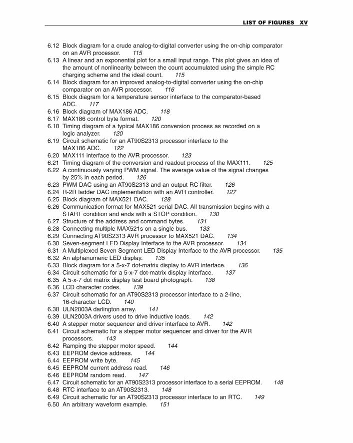
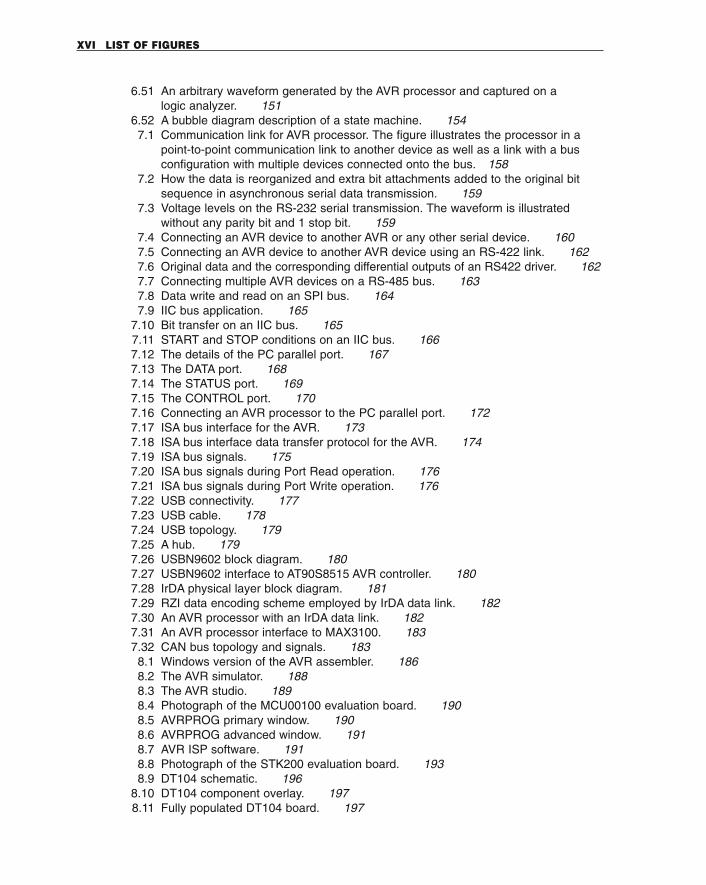
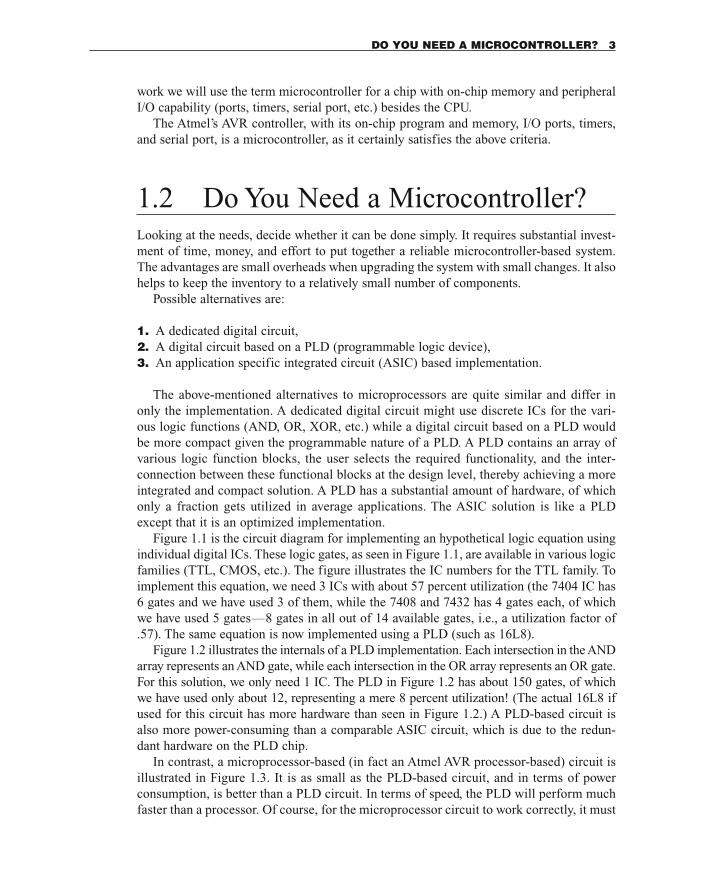
Figure 1.1 is the circuit diagram for implementing an hypothetical logic equation usingindividual digital ICs. These logic gates, as seen in Figure 1.1, are available in various logicfamilies (TTL, CMOS, etc.). The figure illustrates the IC numbers for the TTL family. Toimplement this equation, we need 3 ICs with about 57 percent utilization (the 7404 IC has6 gates and we have used 3 of them, while the 7408 and 7432 has 4 gates each, of whichwe have used 5 gates—8 gates in all out of 14 available gates, i.e., a utilization factor of.57). The same equation is now implemented using a PLD (such as 16L8).
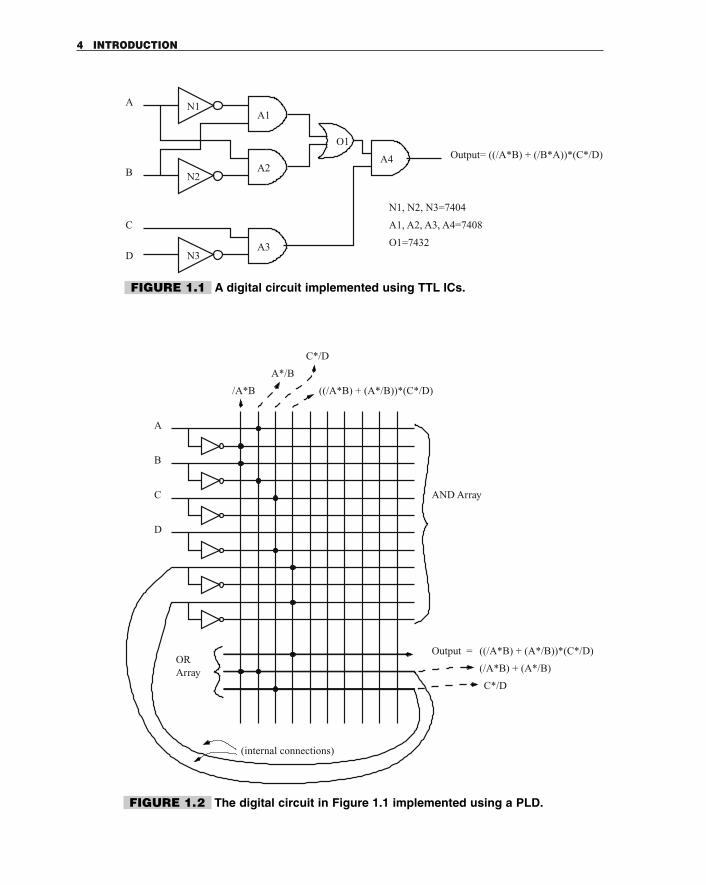
Figure 1.2 illustrates the internals of a PLD implementation. Each intersection in the ANDarray represents an AND gate, while each intersection in the OR array represents an OR gate.For this solution, we only need 1 IC. The PLD in Figure 1.2 has about 150 gates, of whichwe have used only about 12, representing a mere 8 percent utilization! (The actual 16L8 ifused for this circuit has more hardware than seen in Figure 1.2.) A PLD-based circuit isalso more power-consuming than a comparable ASIC circuit, which is due to the redun-dant hardware on the PLD chip.
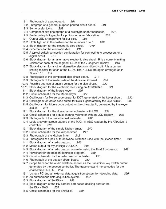
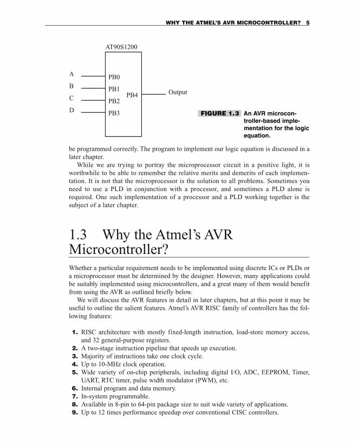
In contrast, a microprocessor-based (in fact an Atmel AVR processor-based) circuit isillustrated in Figure 1.3. It is as small as the PLD-based circuit, and in terms of powerconsumption, is better than a PLD circuit. In terms of speed, the PLD will perform muchfaster than a processor. Of course, for the microprocessor circuit to work correctly, it must
DO YOU NEED A MICROCONTROLLER? 3
4 INTRODUCTION
A
B
C
D
O1
A4A2
A1
A3
N2
N1
N3
Output= ((/A*B) + (/B*A))*(C*/D)
N1, N2, N3=7404
A1, A2, A3, A4=7408
O1=7432
A
B
C
D
Output
AND Array
ArrayOR
/A*B
(/A*B) + (A*/B)
C*/D
C*/D
((/A*B) + (A*/B))*(C*/D)
= ((/A*B) + (A*/B))*(C*/D)
A*/B
(internal connections)
FIGURE 1.1 A digital circuit implemented using TTL ICs.
FIGURE 1.2 The digital circuit in Figure 1.1 implemented using a PLD.
be programmed correctly. The program to implement our logic equation is discussed in alater chapter.
While we are trying to portray the microprocessor circuit in a positive light, it isworthwhile to be able to remember the relative merits and demerits of each implemen-tation. It is not that the microprocessor is the solution to all problems. Sometimes youneed to use a PLD in conjunction with a processor, and sometimes a PLD alone isrequired. One such implementation of a processor and a PLD working together is thesubject of a later chapter.
1.3 Why the Atmel’s AVRMicrocontroller?Whether a particular requirement needs to be implemented using discrete ICs or PLDs ora microprocessor must be determined by the designer. However, many applications couldbe suitably implemented using microcontrollers, and a great many of them would benefitfrom using the AVR as outlined briefly below.
We will discuss the AVR features in detail in later chapters, but at this point it may beuseful to outline the salient features. Atmel’s AVR RISC family of controllers has the fol-lowing features:
1. RISC architecture with mostly fixed-length instruction, load-store memory access,and 32 general-purpose registers.
2. A two-stage instruction pipeline that speeds up execution.3. Majority of instructions take one clock cycle.4. Up to 10-MHz clock operation.5. Wide variety of on-chip peripherals, including digital I/O, ADC, EEPROM, Timer,
UART, RTC timer, pulse width modulator (PWM), etc.6. Internal program and data memory.7. In-system programmable.8. Available in 8-pin to 64-pin package size to suit wide variety of applications.9. Up to 12 times performance speedup over conventional CISC controllers.
WHY THE ATMEL’S AVR MICROCONTROLLER? 5
AT90S1200
A
B
C
D
Output
PB0
PB1
PB2
PB3
PB4
FIGURE 1.3 An AVR microcon-troller-based imple-mentation for the logicequation.
10. Wide operating voltage from 2.7 V to 6.0 V.11. A simple architecture offers a small learning curve to the uninitiated.
What does the name AVR stand for? Atmel says that it is just a name. However, AVRseems to have the initials of the people who designed the controller.
1.4 Organization of This BookThe book has three logical sections:
1. Introduction and preliminary discussion about microcontrollers and AVR controllerdetails. These are covered in Chapters 1 to 4.
2. System design using the AVR RISC controllers. Issues include system design, codedevelopment, software and hardware interfacing the AVR to the outside world. Theseaspects are covered in Chapters 5 to 9.
3. Sample applications are covered in the rest of the chapters, and these illustrate how theAVR controller could be used in real applications.
The idea is to present the material in a format that is easily accessible to readers of vary-ing interests. Beginners could start from the initial chapters and work their way up till thevery end. An individual with some experience with microcontrollers could, on the otherhand, skip the initial chapters in Section 1 and pick up where new material is presented.However, the last section on applications could be a starting point for beginners as well asexperienced users to give perspective. The sample applications illustrate the various waysin which this versatile family of controllers could be used and could well be a starting pointfor a beginner.
The middle sections deal with the specifics of the AVR controller family and how to getan application up and running, how to develop code, and the various tools available in theform of assemblers, compilers, simulators, evaluation and prototyping boards. I have sam-pled a few of these commercial and freeware offerings, and I present my opinion aboutthese products in these sections.
1.5 Timing Diagram ConventionsTiming diagrams are the key to understanding digital circuits and systems. Timing dia-grams illustrate how the signals of a circuit vary as a function of time, as well as the inter-play between the signals. They are the starting point in describing the way a circuit or asystem ought to work, and after a circuit has been designed, the timing diagrams tell thereaders how the circuit or the system works. In turn, if this circuit is being used as a sub-system in a larger design, its associated timing diagram will determine how it fits into thelarger system or how the larger system is to be designed to accommodate the smaller sub-circuit. (Figure 1.4.)
6 INTRODUCTION
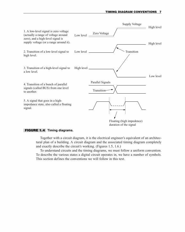
Together with a circuit diagram, it is the electrical engineer’s equivalent of an architec-tural plan of a building. A circuit diagram and the associated timing diagram completelyand exactly describe the circuit’s working. (Figures 1.5, 1.6.)
To understand circuits and the timing diagrams, we must follow a uniform convention.To describe the various states a digital circuit operates in, we have a number of symbols.This section defines the conventions we will follow in this text.
TIMING DIAGRAM CONVENTIONS 7
signal.impedance state, also called a floating5. A signal that goes in a high-
a low level.3. Transition of a high-level signal to
high level.2. Transition of a low-level signal to
supply voltage (or a range around it).zero), and a high-level signal is (actually a range of voltage around1. A low-level signal is zero voltage
4. Transition of a bunch of parallelsignals (called BUS) from one levelto another.
Low levelZero Voltage
Supply VoltageHigh level
High level
TransitionLow level
High level
Low level
Floating (high impedence)duration of the signal
Transition
Parallel Signals
FIGURE 1.4 Timing diagrams.
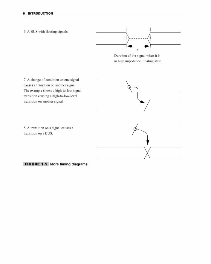
8 INTRODUCTION
Duration of the signal when it is
in high impedance, floating state
The example shows a high-to-low signal
transition on a BUS.
8. A transition on a signal causes a
transition on another signal.
transition causing a high-to-low-level
7. A change of condition on one signal
6. A BUS with floating signals.
causes a transition on another signal.
FIGURE 1.5 More timing diagrams.
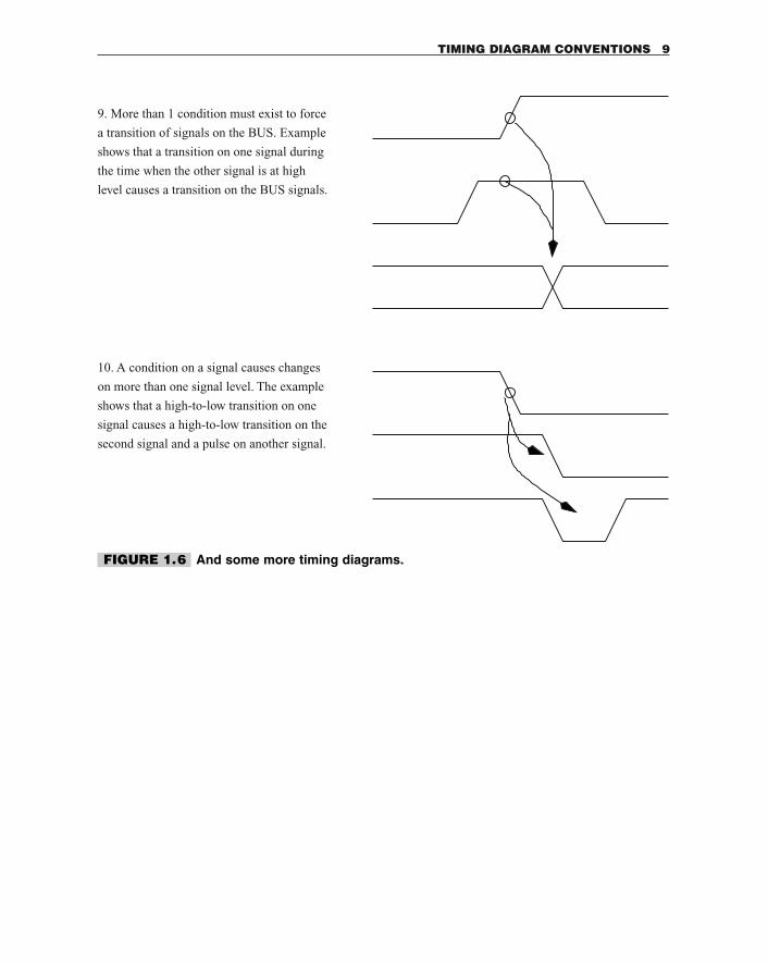
TIMING DIAGRAM CONVENTIONS 9
FIGURE 1.6 And some more timing diagrams.
second signal and a pulse on another signal.
signal causes a high-to-low transition on the
shows that a high-to-low transition on one
on more than one signal level. The example
10. A condition on a signal causes changes
level causes a transition on the BUS signals.
the time when the other signal is at high
shows that a transition on one signal during
a transition of signals on the BUS. Example
9. More than 1 condition must exist to force

This page intentionally left blank.
In this chapter we will briefly outline the history of microcontrollers and then partitionthe various devices in different categories. But before that, let’s take a fresh look at what amicrocontroller is and what can it do for us.
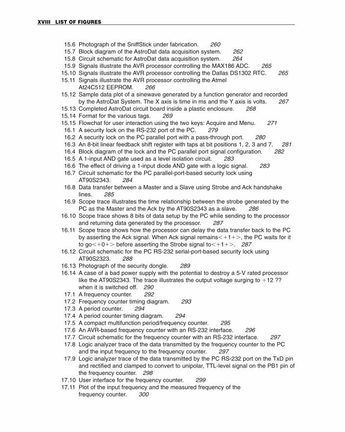
Microcontrollers are fun. They are the heart and soul of many everyday appliances.And most of all, microcontrollers are easy to use and to design with, from the point ofview of a designer. Figure 2.1 is the block diagram of what a typical modern microcon-troller, and especially those in the AVR series, can do. The block in the center of the fig-ure represents the microcontroller. It can interface to motors, a variety of displays as out-put devices, communicate to PCs, read external sensor values, even connect to a networkof similar controllers, and it can do all that without a lot of extra components. This leadsto a small and compact system that is more reliable and cost-effective (because of thefewer number of components and the fewer number of interconnections).
Contrast that with a situation where you don’t have the microcontroller: You only havea CPU. To build a system to interface to various devices (motors, displays, etc.) youwould need external program memory and RAM besides the other required peripheralinterface components needed to connect the motors, displays, sensors, etc., to the CPUchip. Imagine the number of additional components! Rather than being a single-chipsystem, you would end up with a system with a board full of components with increasedpower consumption.
Let us look at the various microcontroller components.
2MICROCONTROLLERS
11
Copyright 2001 The McGraw-Hill Companies, Inc. Click Here for Terms of Use.
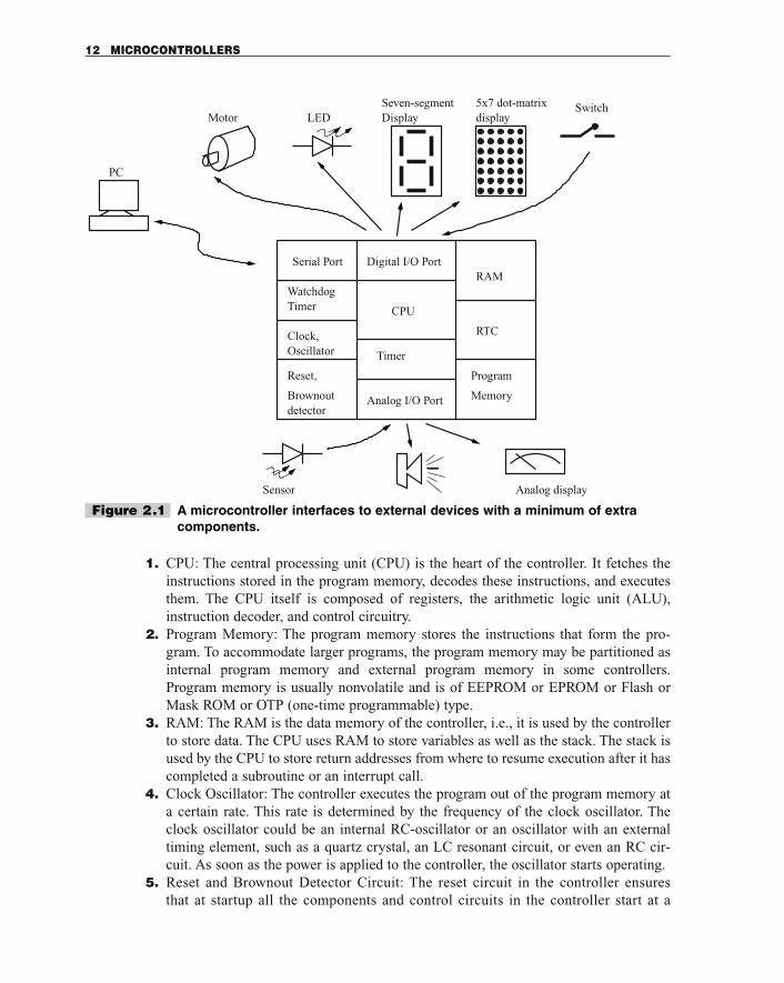
1. CPU: The central processing unit (CPU) is the heart of the controller. It fetches theinstructions stored in the program memory, decodes these instructions, and executesthem. The CPU itself is composed of registers, the arithmetic logic unit (ALU),instruction decoder, and control circuitry.
2. Program Memory: The program memory stores the instructions that form the pro-gram. To accommodate larger programs, the program memory may be partitioned asinternal program memory and external program memory in some controllers.Program memory is usually nonvolatile and is of EEPROM or EPROM or Flash orMask ROM or OTP (one-time programmable) type.
3. RAM: The RAM is the data memory of the controller, i.e., it is used by the controllerto store data. The CPU uses RAM to store variables as well as the stack. The stack isused by the CPU to store return addresses from where to resume execution after it hascompleted a subroutine or an interrupt call.
4. Clock Oscillator: The controller executes the program out of the program memory ata certain rate. This rate is determined by the frequency of the clock oscillator. Theclock oscillator could be an internal RC-oscillator or an oscillator with an externaltiming element, such as a quartz crystal, an LC resonant circuit, or even an RC cir-cuit. As soon as the power is applied to the controller, the oscillator starts operating.
5. Reset and Brownout Detector Circuit: The reset circuit in the controller ensuresthat at startup all the components and control circuits in the controller start at a
12 MICROCONTROLLERS
Sensor Analog display
RAMSerial Port
Watchdog Timer
Reset,
Clock,Oscillator
Memory
Program
RTC
Motor Display5x7 dot-matrixdisplay
PC
LEDSeven-segment Switch
Brownoutdetector
CPU
Timer
Digital I/O Port
Analog I/O Port
Figure 2.1 A microcontroller interfaces to external devices with a minimum of extracomponents.
predefined initial state and all the required registers are initialized properly. Thebrownout detector is a circuit that monitors the power supply voltage, and if thereis a momentary drop in voltage, resets the processor so that the drop in voltagedoes not corrupt register and memory contents, which could lead to faulty opera-tion of the controller.
6. Serial Port: The serial port is a very useful component on the controller. It is used tocommunicate with external devices on a serial data basis. The serial port can operateat any required data transfer speed. The serial port takes data bytes from the controllerand shifts out the data one bit at a time to the output. Similarly, it accepts external dataa bit at a time, makes a byte out of 8 such bits, and presents this to the controller. Serialports are of two types: synchronous and asynchronous. Synchronous data transferneeds an accompanying clock signal with each data bit for timing information, whilethe asynchronous data transfer does not need the clock signal, and the timing infor-mation and synchronization is embedded in the data bit itself by way of duration ofdata bits as well as additional start- and stop-bits on the data path.
7. Digital I/O Port: The microcontroller uses the digital I/O components to exchange dig-ital data with the outside world. Compared to the serial port, which transfers data seri-ally one bit at a time, the data on the digital I/O port is exchanged as bytes.
8. Analog I/O Port: Analog input is performed using an analog-to-digital converter(ADC). The controller could be equipped with an integrated ADC or an analog com-parator, which is used under software control to perform A-to-D conversion. ADCs areused to acquire sensor data from devices such as temperature sensors and pressuresensors; such sensors often produce proportional analog voltage data. Analog outputis performed using a digital-to-analog converter (DAC). Most controllers are equippedwith pulse-width modulators that can be used to get analog voltage with a suitableexternal RC filter. DACs are used to drive motors, for visual displays (of the older VUmeter types), to generate sound or music, etc.
9. Timer: The timer is used by the controller to time events; e.g., it may be required tooutput data to a display at some rate. The timer would be used by the controller to gen-erate that rate. The timer can also be used to count events, external as well as internal.In that case the timer is called a counter.
10. Watchdog Timer: A watchdog timer (WDT) is a special timer with a specific func-tion. It is usually used to prevent software crashes. It works as follows: Once armed,the WDT increments an internal counter at some rate. If the user program does notreset the counter, the counter overflows, which is used to reset the controller. The usersoftware is programmed suitably, therefore, frequently enough, to reset the WDT togive a sort of “I am alive” indication. The assumption is that if the user program doesnot reset the WDT, it has failed in some way and therefore rather than a system crashor unpredictable system performance, it is better to reset the system.
11. RTC: A real timer clock (RTC) is a special timer with the task of maintaining time ofday, date, etc. It can be used to time-stamp events.
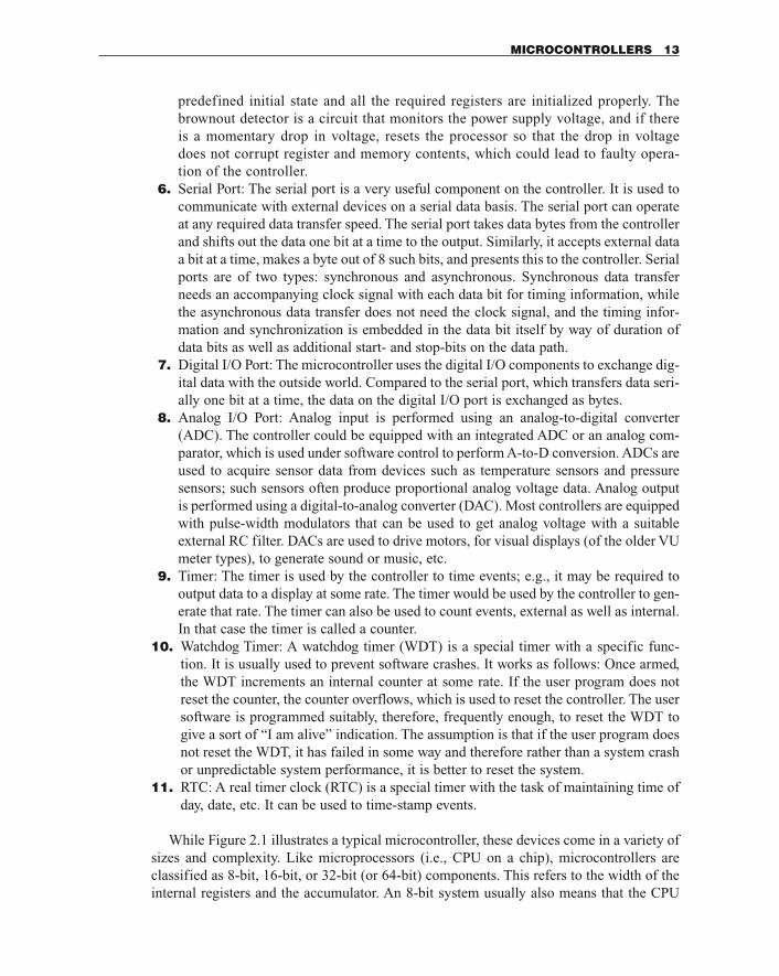
While Figure 2.1 illustrates a typical microcontroller, these devices come in a variety ofsizes and complexity. Like microprocessors (i.e., CPU on a chip), microcontrollers areclassified as 8-bit, 16-bit, or 32-bit (or 64-bit) components. This refers to the width of theinternal registers and the accumulator. An 8-bit system usually also means that the CPU
MICROCONTROLLERS 13
connects to the various chip components through an 8-bit data path. Figure 2.2 illustratesthis concept.
Of the various microcontroller types, 8-bit microcontrollers have the largest marketshare. In 1999, the market for 8-bit chips was $4.8 billion. In comparison, the combined16-bit and 32-bit chip market was merely $452 million only. Smaller 4-bit controllers alsoexist and have a small market share.
Controllers with larger data paths can perform better than similar controllers withsmaller data paths. However, controllers with smaller data paths also have cheaper devel-opment tools compared to controllers with bigger data paths. Eight-bit controllers are themost popular devices not only because of lower device cost (compared to 16- or 32-bitdevices) but also because the development tools for 8-bit devices cost much less, and 8-bitdevices are now being offered with increased performance and more integrated peripheralcomponents.
Besides the classification based on the size of the internal data path, microcontrollersare also classified on the basis of the underlying architecture. The next section looks atarchitectural aspects of the microcontroller.
2.1 Microcontroller ArchitectureMicrocontroller architecture is classified on the basis of various features. One very com-mon classification is on the basis of a number of instructions: CISC (complex instructionset computer), RISC (reduced instruction set computer), or MISC (minimal instruction
14 MICROCONTROLLERS
CPU
ProgramMemory
RAM
Digital I/O
UART(Serial Port)
WatchdogTimer
Timer
Analog I/O
8-bit DATA Bus
Oscillator
Vcc
Gnd
Port Port
Figure 2-2 An 8-bit microcontroller.
set computer). However, these terms have been much muddled by marketing personnel.A CISC processor often has many RISC-like features, and it has become very confusing.
Another classification is on the basis of way the program and data memory is accessed;a unified memory model is called the Princeton or Von Neumann architecture versus theHarvard architecture, which offered separate memory for program storage and data storage.
Another classification is on the basis of the way the internal data is stored and manipu-lated inside the CPU. A microcontroller’s job is to manipulate data. A microcontroller (or amicroprocessor) manipulates data with the help of a user program. The way this data isstored and accessed internally in the CPU and the way it is processed forms the basis of dif-ferent processor architectures and yet another classification scheme. There are four basicmodels: stack, accumulator, register-memory, and register-register (known as load-store).
To understand the differences between these various architectures (on the basis ofinternal data manipulation) let us consider code sequences for performing the followingcomputation:
C � A � B
where A, B, and C are variables.A stack machine performs this computation as follows:
Push APush BSubPop C
In a stack machine, the ALU gets all operands from the stack and stores all operandsback on the stack. To load a variable on the stack, an instruction Push Var is used. A stackoperates by putting the last value on the top. The ALU accesses the top two values on thestack and performs any given operation (addition, subtraction, division, etc.). The result isstored back on the stack at the topmost location.
An accumulator machine performs this computation as follows: In the accumulatormachine, one of the operands is always the accumulator. In fact, all operations are accu-mulator centric.
Load A; Loads accumulator with variable ASub B; subtracts variable B from the contents of the accumulator andstores the result back in accumulator
Store C; stores the value of the accumulator, which has the result, invariable C
A register-memory machine performs this computation as follows:
Load Rx, A; loads a register Rx with variable ASub Rx, B; subtracts the variable B from the contents of register Rxand stores the result in Rx
Store C, Rx; stores the contents of Rx which is the result in variable C
A register-register machine performs this computation as follows:
Load Rx, ALoad Ry, B
MICROCONTROLLER ARCHITECTURE 15
Sub Rz, Rx, RyStore C, Rz
In the register-register model, memory (which stores the variables) is accessed onlyusing the load- and-store instructions. Hence here, the registers are first loaded with thevariable values, the computation is performed with the result back in one of the registers,and the result from this register is stored back in the destination variable.
The register-memory and the register-register architecture processors have a large num-ber of registers that are orthogonal in nature. Any register can be used in any operation.Typically, such architectures have 32 general-purpose registers.
Early processor architectures used either the stack or the accumulator model. However,most modern processors use the register-register architecture. This is because of the real-ization that accessing internal registers is much faster than accessing external memory. Toreduce external memory accesses, a large pool of general-purpose registers is provided forthe register-register model. Moreover, registers are easier to access for a compiler than saya stack, even though the stack is inside the processor.
2.2 Choosing a MicrocontrollerThere are literally hundreds of microprocessors and microcontrollers on the market, andchoosing a particular one for your application can be a nightmare. Usually one starts byenumerating one’s requirements in terms of features and cost and then comparing thesewith what is available. The final choice may still be dictated by other factors such as mar-ket trends, company profile, popularity, local design expertise, etc.
Listed below are some of the popular 8-bit microcontrollers and their features. Thesedevices are the lowest cost-representative devices from respective manufacturers.
COMPANY DEVICE ON-CHIP MEMORY OTHER FEATURES
AB Semicon Ltd AB180-20 Nil Two 16-bit timers, UART, fixed-point 32-bit arithmetic unit,DMA controller
Atmel Corp ATtiny11 1-kbyte flash 8-bit timer, analog comparator,watchdog, on-chip oscillator,one external interrupt
Dallas Semi DS80C310 256-byte RAM Four clocks per machine cycle,UART, three 16-bit timer/coun-ters, dual data pointers, teninternal/six external interrupts,power-on reset
Hitachi H8/3640 8-kbyte ROM Three 8-bit timers, one 16-bit 512 byte RAM timer, one 14-bit PWM timer,
one watchdog, two SCI ports,eight 8-bit ADC, 32-kHz sub-clock generator
16 MICROCONTROLLERS
COMPANY DEVICE MEMORY OTHER FEATURES
Infineon C501 8-kbyte ROM Serial interface, three 16-bit 256-bytes RAM timers, 32 I/O ports
Microchip PIC16CR54C 768-byte ROM, 12 I/O pins, 8-bit timer, high-25-byte RAM current sink/source for direct
LED drive, watchdog timer,RC oscillator
Mitsubishi M37531M4 8-kbyte ROM 2.2 to 5.5V operation; 16-bit-256-byte RAM wide address bus; three 8-bit
timers; 16-bit watchdog timer;10-bit, eight-channel ADC;UART; one clock-synchronizedserial port; one external inter-rupt, seven high-current outputports for LED operation; key-onwake-up function, 29 program-mable-I/O ports, built-in clock-generating circuit
Motorola 68HC705KJ1 1240-byte OTP 15-stage multifunction timer, 64-byte RAM on-chip oscillator, low-voltage
reset, watchdog, keyboardinterrupt, high-current I/O port
NEC 789011 2-kbyte RAM Two 8-bit timers, UART, 22 pro-128-byte RAM grammable I/O ports, two-
channel serial interface
Philips P87LPC762 2-kbyte OTP Oscillator, watchdog, 32-byte 128-byte RAM customer-code EPROM, UART,
I2C, comparators, timers/coun-ters, brown-out detector,power-on reset, keypad wake-up, LED drivers
Samsung KS86C0004 4-kbyte ROM RC oscillator, 12-pin key 208-byte RAM matrix, one 8-bit timer, one
8-bit timer/counter, 14 interruptsources, 32 I/O ports
Scenix SX28AC 3-kbyte flash Analog comparator, program-136-byte RAM mable I/O, brown-out detector,
8-bit timer, watchdog
STMicro ST6203CB1 1 kbyte ROM 8-bit timer, watchdog, nine I/O or OTP lines with high-current capabili-64-byte RAM ty, internal backup oscillator
system, brown-out detection
Toshiba TMP87C405AM 4-kbyte ROM Nine interrupt sources, pro-256-byte RAM grammable watchdog timer, 22
programmable I/O ports
CHOOSING A MICROCONTROLLER 17
COMPANY DEVICE MEMORY OTHER FEATURES
Xemics SA XE8301 22-kbyte ROM Clock prescalar, watchdog 512-byte RAM timer, power-on reset, supply-
level detection, 20-pin pro-grammable I/O, crystal and RCoscillator, UART, four 8-bittimers with PWM
Zilog Z8E000 0.5-kbyte OTP One 16-bit timer, watchdog, 32-byte RAM four hardware interrupts, 13 I/O
pins
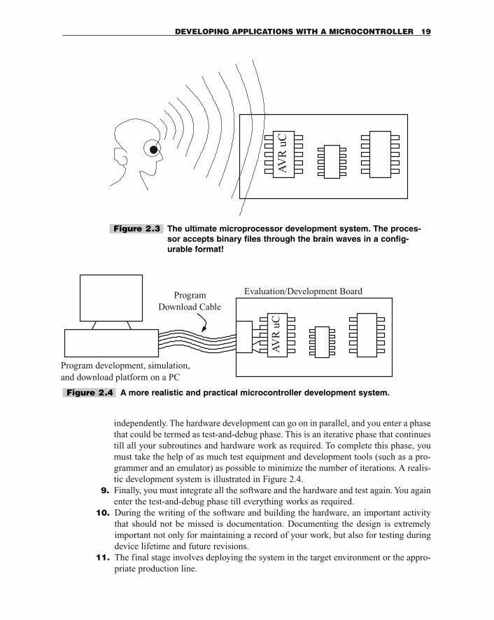
2.3 Developing Applications with a MicrocontrollerNow that we have a little bit of inside information about microcontrollers and what can bedone using them, it is time to discover how to go about developing applications using thesecontrollers.
An ideal and a rather futuristic method is depicted in Figure 2.3. But let us for a momentconsider what all is required to develop applications using controllers.
Let us list one of the possible roadmaps for designing a microcontroller-based device.
1. First and foremost, define the requirements.2. Create sufficient documentation to support the requirements in the form of block dia-
grams, flowcharts, timing diagrams, etc.3. Search for suitable hardware to provide the necessary functionality. This may help the
designer realize whether a microcontroller is needed at all or not.4. If you do need a microcontroller, then identify a suitable microcontroller that can act
as the brains for the device.5. Once you have identified the controller, double-check that in fact the microcontroller
will satisfy the requirements in terms of speed, power consumption, etc. Otherwiseyou will have to iterate once again to choose another controller.
6. As a next step you will need to acquire all the tools to help develop the hardware andthe software. These tools may include an assembler and/or a compiler if you wish toprogram in a high-level language, a simulator for the controller, if possible a hardwareemulator, evaluation board, programmer for the controller, etc.
7. If you are already familiar with this particular controller, you can start designing andassembling a prototype; otherwise, you may need to get familiar with the controllerby writing sample programs and testing them on the evaluation board or on the soft-ware simulator.
8. Once you become familiar with the features of the controller, you can start partition-ing the software in manageable blocks that can be written as subroutines and tested
18 MICROCONTROLLERS
independently. The hardware development can go on in parallel, and you enter a phasethat could be termed as test-and-debug phase. This is an iterative phase that continuestill all your subroutines and hardware work as required. To complete this phase, youmust take the help of as much test equipment and development tools (such as a pro-grammer and an emulator) as possible to minimize the number of iterations. A realis-tic development system is illustrated in Figure 2.4.
9. Finally, you must integrate all the software and the hardware and test again. You againenter the test-and-debug phase till everything works as required.
10. During the writing of the software and building the hardware, an important activitythat should not be missed is documentation. Documenting the design is extremelyimportant not only for maintaining a record of your work, but also for testing duringdevice lifetime and future revisions.
11. The final stage involves deploying the system in the target environment or the appro-priate production line.
DEVELOPING APPLICATIONS WITH A MICROCONTROLLER 19
AV
R u
C
Figure 2.3 The ultimate microprocessor development system. The proces-sor accepts binary files through the brain waves in a config-urable format!
AV
R u
C
Evaluation/Development Board
and download platform on a PCProgram development, simulation,
Download CableProgram
Figure 2.4 A more realistic and practical microcontroller development system.

This page intentionally left blank.
3.1 IntroductionThis chapter describes the AVR processor family in detail, covering the architecturalaspects and the integrated peripheral components that are bundled with the CPU.
The AVR is a RISC processor with a Harvard architecture. The Harvard architecturerefers to the fact that the CPU has a program memory and a separate data memory.
The AVR processor family has the following features:
1. On-chip and In System Programmable Flash memory used as Program Memory. Allthe processors have on-chip flash program memory. This means you don’t have tohave external EPROMs or ROMs containing your program code. Also, the programmemory can be programmed while the processor is in the target without removing it.This allows faster and easier system software upgrades. The program memory can beprogrammed in situ (i.e., without removing from the target system). The programmemory can be programmed in two modes: serial and parallel, which we will discusslater.
2. 32-X-8 general-purpose working registers (in the true RISC tradition). A large regis-ter set means that variables can be stored inside the CPU rather than storing the vari-ables in memory, as accessing memory, is time expensive. Thus the program will runfaster.
3THE AVR RISC MICROCONTROLLER
ARCHITECTURE
21
Copyright 2001 The McGraw-Hill Companies, Inc. Click Here for Terms of Use.
3. On-chip data memory EEPROM and RAM in most devices. The CPU is Harvardarchitecture, and the EEPROM and the RAM is seen as DATA memory for storingconstants and variables.
4. 0 to 10-MHz clock speed operation. Most instructions operate in 1 clock cycle, andthis leads to an almost 10-times performance improvement over conventional proces-sors (e.g., the 8051) operating at equal clock frequency.
5. Power On RESET circuit.6. On-chip programmable timer with separate prescalar. This is used for timing applica-
tions.7. Internal and external interrupt sources.8. Programmable watchdog timer with independent oscillator. This is used to recover in
case of software crash but can also be used for other interesting applications as dis-cussed in one of the project chapters.
9. SLEEP and POWER DOWN modes of operation. This saves power when the proces-sor is idling.
10. Many chips with on-chip RC clock oscillator. Using the on-chip RC oscillator featurewhen available leads to an even lower component count.
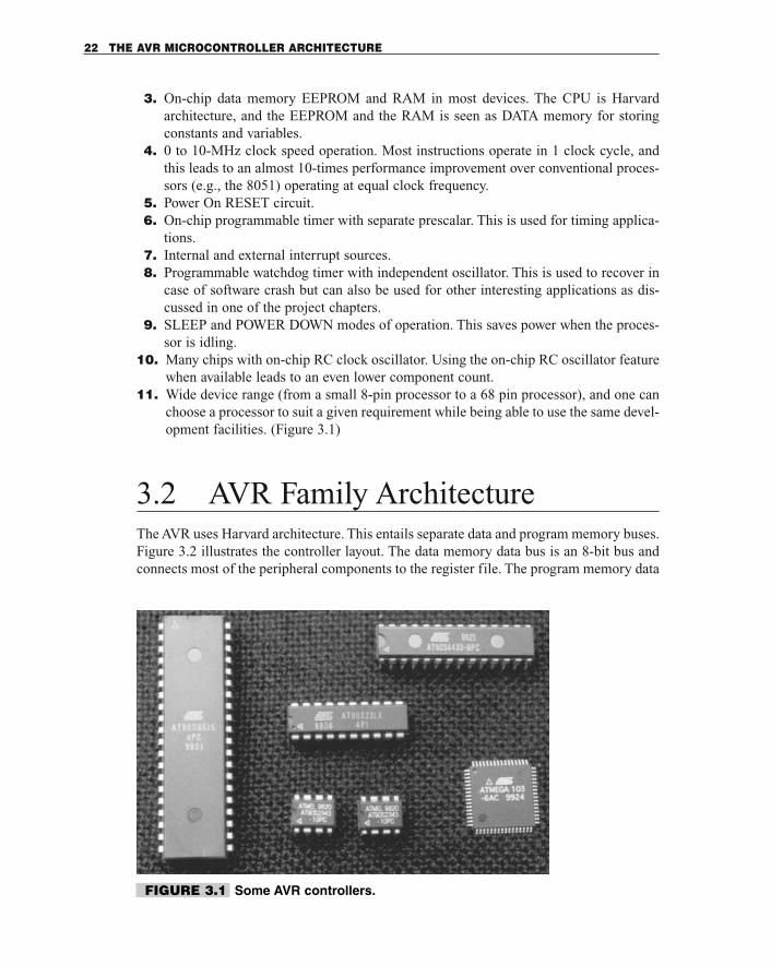
11. Wide device range (from a small 8-pin processor to a 68 pin processor), and one canchoose a processor to suit a given requirement while being able to use the same devel-opment facilities. (Figure 3.1)
3.2 AVR Family ArchitectureThe AVR uses Harvard architecture. This entails separate data and program memory buses.Figure 3.2 illustrates the controller layout. The data memory data bus is an 8-bit bus andconnects most of the peripheral components to the register file. The program memory data
22 THE AVR MICROCONTROLLER ARCHITECTURE
FIGURE 3.1 Some AVR controllers.
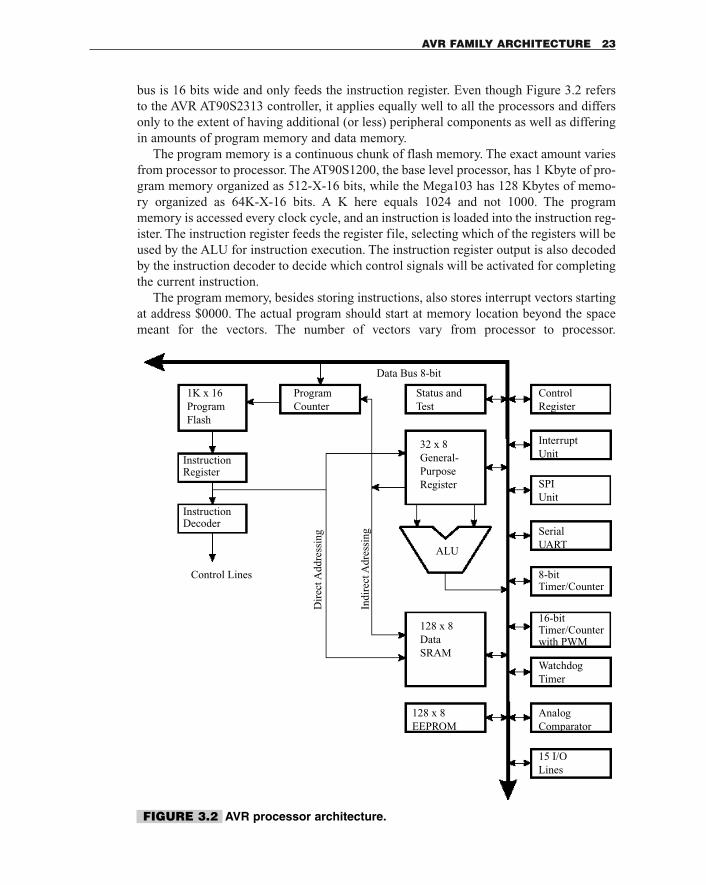
bus is 16 bits wide and only feeds the instruction register. Even though Figure 3.2 refersto the AVR AT90S2313 controller, it applies equally well to all the processors and differsonly to the extent of having additional (or less) peripheral components as well as differingin amounts of program memory and data memory.
The program memory is a continuous chunk of flash memory. The exact amount variesfrom processor to processor. The AT90S1200, the base level processor, has 1 Kbyte of pro-gram memory organized as 512-X-16 bits, while the Mega103 has 128 Kbytes of memo-ry organized as 64K-X-16 bits. A K here equals 1024 and not 1000. The program memory is accessed every clock cycle, and an instruction is loaded into the instruction reg-ister. The instruction register feeds the register file, selecting which of the registers will beused by the ALU for instruction execution. The instruction register output is also decodedby the instruction decoder to decide which control signals will be activated for completingthe current instruction.
The program memory, besides storing instructions, also stores interrupt vectors startingat address $0000. The actual program should start at memory location beyond the spacemeant for the vectors. The number of vectors vary from processor to processor.
AVR FAMILY ARCHITECTURE 23
ProgramCounter
Status andTest
1K x 16ProgramFlash
Instruction
InstructionDecoder
Register
32 x 8General-PurposeRegister
ALU
128 x 8DataSRAM
128 x 8EEPROM
ControlRegister
InterruptUnit
SPIUnit
SerialUART
8-bitTimer/Counter
16-bitTimer/Counterwith PWM
WatchdogTimer
AnalogComparator
15 I/OLines
Control Lines
Data Bus 8-bitIn
dire
ct A
dres
sing
Dir
ect A
ddre
ssin
g
FIGURE 3.2 AVR processor architecture.
AT90S1200 has 3 vectors and AT90S8515 has 13 vectors. Table 3.1 illustrates the com-plete vector space for AT90S8515.
The data memory, on the other hand, is split up in different types. Figure 3.3 has the var-ious memory maps available to an AVR processor. The data memory has in all five different components:
1. A register file with 32 registers of 8-bit width. All processors of the AVR family havethis register file.
2. 64 I/O registers of 8 bits each. All the processors do not have all the 64 registers. Somehave more than others, depending on the number of peripheral components on the chip.These registers are really part of on-chip SRAM and can be accessed either as SRAMwith addresses between $20 and $5F or as I/O registers with addresses between $00 and$3F. Most often, all of these registers are accessed as I/O registers rather than asSRAM.
3. Internal SRAM. This is available on most of the AVR processors except the baselineprocessors such as the AT90S1200. The amount of SRAM varies between 128 bytes to 4Kbytes. The SRAM is used for stack as well as storing variables. During interrupts andsubroutine calls, the current program counter value is stored on the stack. The size of thestack is limited by the available on-chip SRAM. The current stack location is indicatedby the stack pointer. The stack pointer is 1 byte on smaller processors such as AT90S2313and is 2 bytes on larger processors such as the AT90S8515. The stack pointer must be ini-tialized after reset and before the stack can be used. For those processors that do not haveon-chip SRAM such as the AT90S1200, a hardware stack is available to store programreturn addresses. This hardware stack can only store up to 3 return addresses.
24 THE AVR MICROCONTROLLER ARCHITECTURE
TABLE 3-1 PROGRAM MEMORY VECTOR SPACE FOR AT90S8515
PROGRAM MEMORY ADDRESS VECTOR COMMENTS
$0000 Reset Reset handler
$0001 EXT_INT0 IRQ0 handler
$0002 EXT_INT1 IRQ1 handler
$0003 TIM_CAPT Timer1 capture handler
$0004 TIM1_COMA Timer1 compareA handler
$0005 TIM1_COMB Timer1 compareB handler
$0006 TIM1_OVF Timer1 overflow handler
$0007 TIM0_OVF Timer0 overflow handler
$0008 SPI_STC SPI transfer complete handler
$0009 UART_RXC UART RX complete handler
$000A UART_DRE UART UDR empty handler
$000B UART_TXC UAT TXC complete handler
$000C ANA_COMP Analog comparator handler
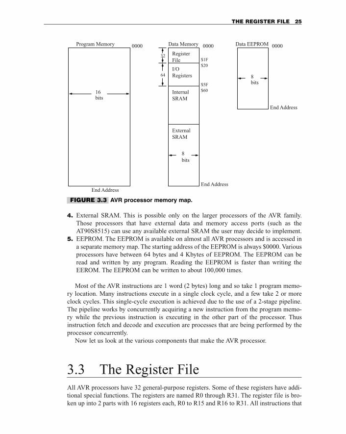
4. External SRAM. This is possible only on the larger processors of the AVR family.Those processors that have external data and memory access ports (such as theAT90S8515) can use any available external SRAM the user may decide to implement.
5. EEPROM. The EEPROM is available on almost all AVR processors and is accessed ina separate memory map. The starting address of the EEPROM is always $0000. Variousprocessors have between 64 bytes and 4 Kbytes of EEPROM. The EEPROM can beread and written by any program. Reading the EEPROM is faster than writing theEEROM. The EEPROM can be written to about 100,000 times.
Most of the AVR instructions are 1 word (2 bytes) long and so take 1 program memo-ry location. Many instructions execute in a single clock cycle, and a few take 2 or moreclock cycles. This single-cycle execution is achieved due to the use of a 2-stage pipeline.The pipeline works by concurrently acquiring a new instruction from the program memo-ry while the previous instruction is executing in the other part of the processor. Thusinstruction fetch and decode and execution are processes that are being performed by theprocessor concurrently.
Now let us look at the various components that make the AVR processor.
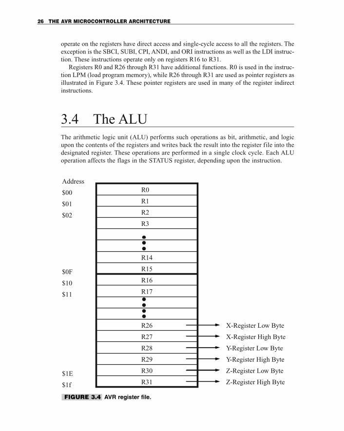
3.3 The Register FileAll AVR processors have 32 general-purpose registers. Some of these registers have addi-tional special functions. The registers are named R0 through R31. The register file is bro-ken up into 2 parts with 16 registers each, R0 to R15 and R16 to R31. All instructions that
THE REGISTER FILE 25
Program Memory 0000
End Address
16bits
Data EEPROM 0000
End Address
8bits
Data Memory
RegisterFile
I/ORegisters
InternalSRAM
ExternalSRAM
0000
End Address
8bits
$1F$20
$5F$60
32
64
FIGURE 3.3 AVR processor memory map.
operate on the registers have direct access and single-cycle access to all the registers. Theexception is the SBCI, SUBI, CPI, ANDI, and ORI instructions as well as the LDI instruc-tion. These instructions operate only on registers R16 to R31.
Registers R0 and R26 through R31 have additional functions. R0 is used in the instruc-tion LPM (load program memory), while R26 through R31 are used as pointer registers asillustrated in Figure 3.4. These pointer registers are used in many of the register indirectinstructions.
3.4 The ALUThe arithmetic logic unit (ALU) performs such operations as bit, arithmetic, and logicupon the contents of the registers and writes back the result into the register file into thedesignated register. These operations are performed in a single clock cycle. Each ALUoperation affects the flags in the STATUS register, depending upon the instruction.
26 THE AVR MICROCONTROLLER ARCHITECTURE
R1
R2
R3
R14
R15
R16
R17
R31
R30
R29
R28
R27
R26
R0Address
$00
$01
$02
$0F
$10
$11
$1E
$1f
X-Register Low Byte
X-Register High Byte
Y-Register Low Byte
Y-Register High Byte
Z-Register Low Byte
Z-Register High Byte
FIGURE 3.4 AVR register file.
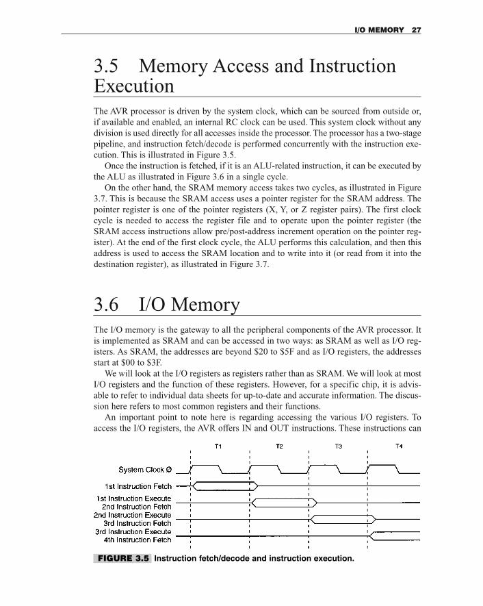
3.5 Memory Access and InstructionExecutionThe AVR processor is driven by the system clock, which can be sourced from outside or,if available and enabled, an internal RC clock can be used. This system clock without anydivision is used directly for all accesses inside the processor. The processor has a two-stagepipeline, and instruction fetch/decode is performed concurrently with the instruction exe-cution. This is illustrated in Figure 3.5.
Once the instruction is fetched, if it is an ALU-related instruction, it can be executed bythe ALU as illustrated in Figure 3.6 in a single cycle.
On the other hand, the SRAM memory access takes two cycles, as illustrated in Figure3.7. This is because the SRAM access uses a pointer register for the SRAM address. Thepointer register is one of the pointer registers (X, Y, or Z register pairs). The first clockcycle is needed to access the register file and to operate upon the pointer register (theSRAM access instructions allow pre/post-address increment operation on the pointer reg-ister). At the end of the first clock cycle, the ALU performs this calculation, and then thisaddress is used to access the SRAM location and to write into it (or read from it into thedestination register), as illustrated in Figure 3.7.
3.6 I/O MemoryThe I/O memory is the gateway to all the peripheral components of the AVR processor. Itis implemented as SRAM and can be accessed in two ways: as SRAM as well as I/O reg-isters. As SRAM, the addresses are beyond $20 to $5F and as I/O registers, the addressesstart at $00 to $3F.
We will look at the I/O registers as registers rather than as SRAM. We will look at mostI/O registers and the function of these registers. However, for a specific chip, it is advis-able to refer to individual data sheets for up-to-date and accurate information. The discus-sion here refers to most common registers and their functions.
An important point to note here is regarding accessing the various I/O registers. Toaccess the I/O registers, the AVR offers IN and OUT instructions. These instructions can
I/O MEMORY 27
FIGURE 3.5 Instruction fetch/decode and instruction execution.
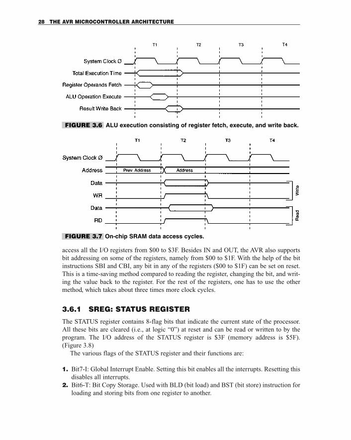
access all the I/O registers from $00 to $3F. Besides IN and OUT, the AVR also supportsbit addressing on some of the registers, namely from $00 to $1F. With the help of the bitinstructions SBI and CBI, any bit in any of the registers ($00 to $1F) can be set on reset.This is a time-saving method compared to reading the register, changing the bit, and writ-ing the value back to the register. For the rest of the registers, one has to use the othermethod, which takes about three times more clock cycles.
3.6.1 SREG: STATUS REGISTER
The STATUS register contains 8-flag bits that indicate the current state of the processor.All these bits are cleared (i.e., at logic “0”) at reset and can be read or written to by theprogram. The I/O address of the STATUS register is $3F (memory address is $5F). (Figure 3.8)
The various flags of the STATUS register and their functions are:
1. Bit7-I: Global Interrupt Enable. Setting this bit enables all the interrupts. Resetting thisdisables all interrupts.
2. Bit6-T: Bit Copy Storage. Used with BLD (bit load) and BST (bit store) instruction forloading and storing bits from one register to another.
28 THE AVR MICROCONTROLLER ARCHITECTURE
FIGURE 3.6 ALU execution consisting of register fetch, execute, and write back.
FIGURE 3.7 On-chip SRAM data access cycles.
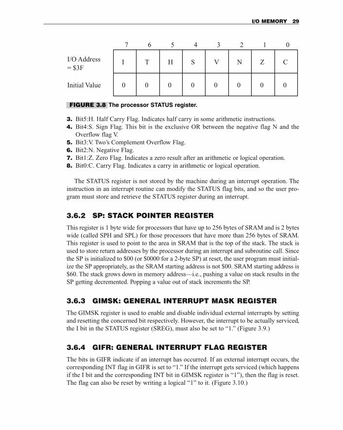
3. Bit5:H. Half Carry Flag. Indicates half carry in some arithmetic instructions.4. Bit4:S. Sign Flag. This bit is the exclusive OR between the negative flag N and the
Overflow flag V.5. Bit3:V. Two’s Complement Overflow Flag.6. Bit2:N. Negative Flag.7. Bit1:Z. Zero Flag. Indicates a zero result after an arithmetic or logical operation.8. Bit0:C. Carry Flag. Indicates a carry in arithmetic or logical operation.
The STATUS register is not stored by the machine during an interrupt operation. Theinstruction in an interrupt routine can modify the STATUS flag bits, and so the user pro-gram must store and retrieve the STATUS register during an interrupt.
3.6.2 SP: STACK POINTER REGISTER
This register is 1 byte wide for processors that have up to 256 bytes of SRAM and is 2 byteswide (called SPH and SPL) for those processors that have more than 256 bytes of SRAM.This register is used to point to the area in SRAM that is the top of the stack. The stack isused to store return addresses by the processor during an interrupt and subroutine call. Sincethe SP is initialized to $00 (or $0000 for a 2-byte SP) at reset, the user program must initial-ize the SP appropriately, as the SRAM starting address is not $00. SRAM starting address is$60. The stack grows down in memory address—i.e., pushing a value on stack results in theSP getting decremented. Popping a value out of stack increments the SP.
3.6.3 GIMSK: GENERAL INTERRUPT MASK REGISTER
The GIMSK register is used to enable and disable individual external interrupts by settingand resetting the concerned bit respectively. However, the interrupt to be actually serviced,the I bit in the STATUS register (SREG), must also be set to “1.” (Figure 3.9.)
3.6.4 GIFR: GENERAL INTERRUPT FLAG REGISTER
The bits in GIFR indicate if an interrupt has occurred. If an external interrupt occurs, thecorresponding INT flag in GIFR is set to “1.” If the interrupt gets serviced (which happensif the I bit and the corresponding INT bit in GIMSK register is “1”), then the flag is reset.The flag can also be reset by writing a logical “1” to it. (Figure 3.10.)
I/O MEMORY 29
I T H S V N Z C
01234567
0 0 0 0 0 0 0 0
I/O Address= $3F
Initial Value
FIGURE 3.8 The processor STATUS register.
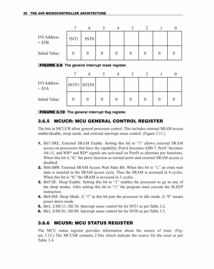
3.6.5 MCUCR: MCU GENERAL CONTROL REGISTER
The bits in MCUCR allow general processor control. This includes external SRAM accessenable/disable, sleep mode, and external interrupt sense control. (Figure 3.11.)
1. Bit7:SRE. External SRAM Enable. Setting this bit to “1” allows external SRAMaccess on processors that have the capability. PortA becomes AD0-7, PortC becomesA8-15, and WR* and RD* signals are activated on PortD as alternate pin functions.When this bit is “0,” the ports function as normal ports and external SRAM access isdisabled.
2. Bit6:SRW. External SRAM Access Wait State Bit. When this bit is “1,” an extra waitstate is inserted in the SRAM access cycle. Thus the SRAM is accessed in 4 cycles.When this bit is “0,” the SRAM is accessed in 3 cycles.
3. Bit5:SE. Sleep Enable. Setting this bit to “1” enables the processor to go in one of the sleep modes. After setting this bit to “1,” the program must execute the SLEEPinstruction.
4. Bit4:SM. Sleep Mode. A “1” in this bit puts the processor in idle mode. A “0” meanspower down mode.
5. Bit3, 2:ISC11, ISC10. Interrupt sense control bit for INT1 as per Table 3.2.6. Bit1, 0:ISC01, ISC00. Interrupt sense control bit for INT0 as per Table 3.3.
3.6.6 MCUSR: MCU STATUS REGISTER
The MCU status register provides information about the source of reset. (Fig-ure 3.12.) The MCUSR contains 2 bits which indicate the source for the reset as perTable 3.4.
30 THE AVR MICROCONTROLLER ARCHITECTURE
01234567
0 0 0 0 0 0 0 0
I/O Address
Initial Value
= $3BINT1 INT0
FIGURE 3.9 The general interrupt mask register.
01234567
0 0 0 0 0 0 0 0
I/O Address
Initial Value
INTF1 INTF0= $3A
FIGURE 3.10 The general interrupt flag register.
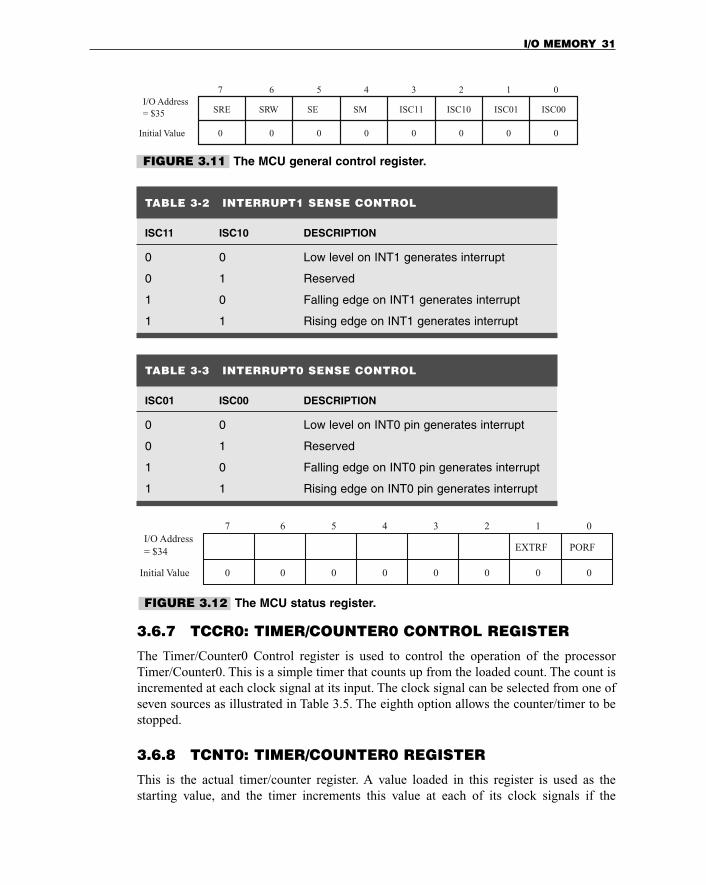
3.6.7 TCCR0: TIMER/COUNTER0 CONTROL REGISTER
The Timer/Counter0 Control register is used to control the operation of the processorTimer/Counter0. This is a simple timer that counts up from the loaded count. The count isincremented at each clock signal at its input. The clock signal can be selected from one ofseven sources as illustrated in Table 3.5. The eighth option allows the counter/timer to bestopped.
3.6.8 TCNT0: TIMER/COUNTER0 REGISTER
This is the actual timer/counter register. A value loaded in this register is used as the starting value, and the timer increments this value at each of its clock signals if the
I/O MEMORY 31
Initial Value
I/O Address
0 0 0 0 0 0 0 0
7 6 5 4 3 2 1 0
= $35 SE SM ISC01 ISC00SRE SRW ISC11 ISC10
FIGURE 3.11 The MCU general control register.
TABLE 3-2 INTERRUPT1 SENSE CONTROL
ISC11 ISC10 DESCRIPTION
0 0 Low level on INT1 generates interrupt
0 1 Reserved
1 0 Falling edge on INT1 generates interrupt
1 1 Rising edge on INT1 generates interrupt
Initial Value
I/O Address
0 0 0 0 0 0 0 0
7 6 5 4 3 2 1 0
= $34 EXTRF PORF
FIGURE 3.12 The MCU status register.
TABLE 3-3 INTERRUPT0 SENSE CONTROL
ISC01 ISC00 DESCRIPTION
0 0 Low level on INT0 pin generates interrupt
0 1 Reserved
1 0 Falling edge on INT0 pin generates interrupt
1 1 Rising edge on INT0 pin generates interrupt
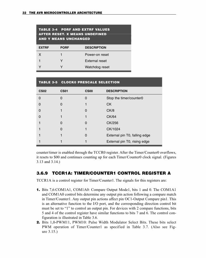
counter/timer is enabled through the TCCR0 register. After the Timer/Counter0 overflows,it resets to $00 and continues counting up for each Timer/Counter0 clock signal. (Figures3.13 and 3.14.)
3.6.9 TCCR1A: TIMER/COUNTER1 CONTROL REGISTER A
TCCR1A is a control register for Timer/Counter1. The signals for this registers are:
1. Bits 7,6:COM1A1, COM1A0: Compare Output Mode1, bits 1 and 0. The COM1A1and COM1A0 control bits determine any output pin action following a compare matchin Timer/Counter1. Any output pin actions affect pin OC1-Output Compare pin1. Thisis an alternative function to the I/O port, and the corresponding direction control bitmust be set to “1” to control an output pin. For devices with 2 compare functions, bits5 and 4 of the control register have similar functions to bits 7 and 6. The control con-figuration is illustrated in Table 3.6.
2. Bits 1,0-PWM11, PWM10: Pulse Width Modulator Select Bits. These bits selectPWM operation of Timer/Counter1 as specified in Table 3.7. (Also see Fig-ure 3.15.)
32 THE AVR MICROCONTROLLER ARCHITECTURE
TABLE 3-4 PORF AND EXTRF VALUES AFTER RESET. X MEANS UNDEFINED AND Y MEANS UNCHANGED
EXTRF PORF DESCRIPTION
X 1 Power-on reset
1 Y External reset
Y Y Watchdog reset
TABLE 3-5 CLOCK0 PRESCALE SELECTION
CS02 CS01 CS00 DESCRIPTION
0 0 0 Stop the timer/counter0
0 0 1 CK
0 1 0 CK/8
0 1 1 CK/64
1 0 0 CK/256
1 0 1 CK/1024
1 1 0 External pin T0, falling edge
1 1 1 External pin T0, rising edge
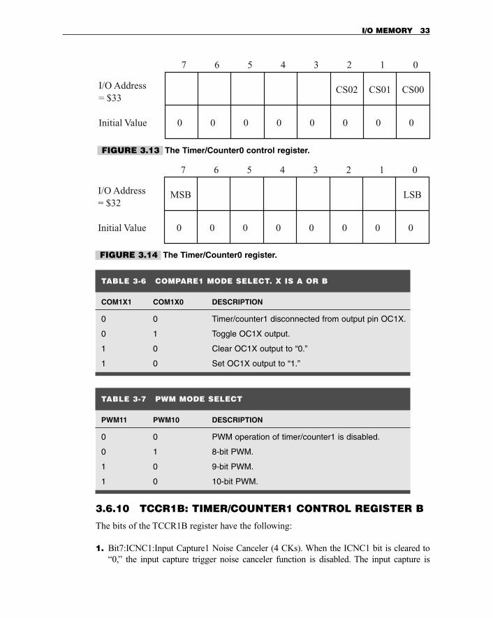
3.6.10 TCCR1B: TIMER/COUNTER1 CONTROL REGISTER B
The bits of the TCCR1B register have the following:
1. Bit7:ICNC1:Input Capture1 Noise Canceler (4 CKs). When the ICNC1 bit is cleared to“0,” the input capture trigger noise canceler function is disabled. The input capture is
I/O MEMORY 33
TABLE 3-6 COMPARE1 MODE SELECT. X IS A OR B
COM1X1 COM1X0 DESCRIPTION
0 0 Timer/counter1 disconnected from output pin OC1X.
0 1 Toggle OC1X output.
1 0 Clear OC1X output to “0.”
1 0 Set OC1X output to “1.”
TABLE 3-7 PWM MODE SELECT
PWM11 PWM10 DESCRIPTION
0 0 PWM operation of timer/counter1 is disabled.
0 1 8-bit PWM.
1 0 9-bit PWM.
1 0 10-bit PWM.
01234567
0 0 0 0 0 0 0 0
I/O Address
Initial Value
= $32MSB LSB
FIGURE 3.14 The Timer/Counter0 register.
01234567
0 0 0 0 0 0 0 0
I/O Address
Initial Value
= $33CS01CS02 CS00
FIGURE 3.13 The Timer/Counter0 control register.
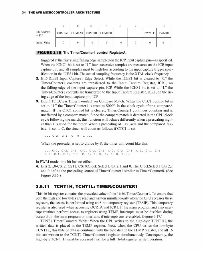
triggered at the first rising/falling edge sampled on the ICP input capture pin—as specified.When the ICNC1 bit is set to “1,” four successive samples are measures on the ICP, inputcapture pin, and all samples must be high/low according to the input capture trigger spec-ification in the ICES1 bit. The actual sampling frequency is the XTAL clock frequency.
2. Bit6:ICES1:Input Capture1 Edge Select. While the ICES1 bit is cleared to “0,” theTimer/Counter1 contents are transferred to the Input Capture Register, ICR1, on the falling edge of the input capture pin, ICP. While the ICES1 bit is set to “1,” theTimer/Counter1 contents are transferred to the Input Capture Register, ICR1, on the ris-ing edge of the input capture pin, ICP.
3. Bit3:CTC1:Clear Timer/Counter1 on Compare Match. When the CTC1 control bit isset to “1,” the Timer/Counter1 is reset to $0000 in the clock cycle after a compareAmatch. If the CTC1 control bit is cleared, Timer/Counter1 continues counting and isunaffected by a compare match. Since the compare match is detected in the CPU clockcycle following the match, this function will behave differently when a prescaling high-er than 1 is used for the timer. When a prescaling of 1 is used, and the compareA reg-ister is set to C, the timer will count as follows if CTC1 is set:
... C-2 C-1 C 0 1 ...
When the prescaler is set to divide by 8, the timer will count like this:
... C-2, C-2, C-2, C-2, C-2, C-2, C-2, C-2 C-1, C-1, C-1, C-1,C-1, C-1, C-1, C-1 C, 0, 0, 0, 0, 0, 0, 0 ...
In PWM mode, this bit has no effect.4. Bits 2,1,0-CS12, CS11, CS10:Clock Select1, bit 2,1 and 0. The ClockSelect1 bits 2,1
and 0 define the prescaling source of Timer/Counter1 similar to Timer/Counter0. (SeeFigure 3.16.)
3.6.11 TCNT1H, TCNT1L: TIMER/COUNTER1
This 16-bit register contains the prescaled value of the 16-bit Timer/Counter1. To ensure thatboth the high and low bytes are read and written simultaneously when the CPU accesses theseregisters, the access is performed using an 8-bit temporary register (TEMP). This temporaryregister is also used when accessing OCR1A and ICR1. If the main program and also inter-rupt routines perform access to registers using TEMP, interrupts must be disabled duringaccess from the main program or interrupts if interrupts are re-enabled. (Figure 3.17.)
TCNT1 Timer/Counter1 Write: When the CPU writes to the high-byte TCNT1H, thewritten data is placed in the TEMP register. Next, when the CPU writes the low-byteTCNT1L, this byte of data is combined with the byte data in the TEMP register, and all 16bits are written to the TCNT1 Timer/Counter1 register simultaneously. Consequently, thehigh-byte TCNT1H must be accessed first for a full 16-bit register write operation.
34 THE AVR MICROCONTROLLER ARCHITECTURE
FIGURE 3.15 The Timer/Counter1 control RegisterA.
01234567
I/O Address= $2F
Initial Value 0 0 0 0 0 0 0 0
COM1A1 COM1A0 COM1B1 COM1B0 PWM11 PWM10
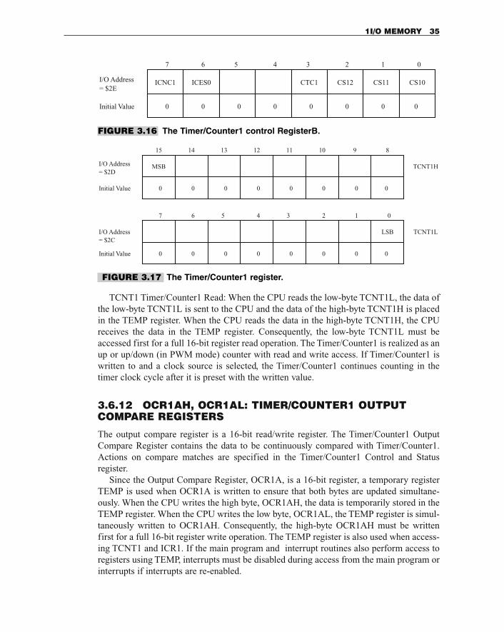
TCNT1 Timer/Counter1 Read: When the CPU reads the low-byte TCNT1L, the data ofthe low-byte TCNT1L is sent to the CPU and the data of the high-byte TCNT1H is placedin the TEMP register. When the CPU reads the data in the high-byte TCNT1H, the CPUreceives the data in the TEMP register. Consequently, the low-byte TCNT1L must beaccessed first for a full 16-bit register read operation. The Timer/Counter1 is realized as anup or up/down (in PWM mode) counter with read and write access. If Timer/Counter1 iswritten to and a clock source is selected, the Timer/Counter1 continues counting in thetimer clock cycle after it is preset with the written value.
3.6.12 OCR1AH, OCR1AL: TIMER/COUNTER1 OUTPUTCOMPARE REGISTERS
The output compare register is a 16-bit read/write register. The Timer/Counter1 OutputCompare Register contains the data to be continuously compared with Timer/Counter1.Actions on compare matches are specified in the Timer/Counter1 Control and Status register.
Since the Output Compare Register, OCR1A, is a 16-bit register, a temporary registerTEMP is used when OCR1A is written to ensure that both bytes are updated simultane-ously. When the CPU writes the high byte, OCR1AH, the data is temporarily stored in theTEMP register. When the CPU writes the low byte, OCR1AL, the TEMP register is simul-taneously written to OCR1AH. Consequently, the high-byte OCR1AH must be writtenfirst for a full 16-bit register write operation. The TEMP register is also used when access-ing TCNT1 and ICR1. If the main program and interrupt routines also perform access toregisters using TEMP, interrupts must be disabled during access from the main program orinterrupts if interrupts are re-enabled.
1I/O MEMORY 35
01234567
I/O Address
Initial Value 0 0 0 0 0 0 0 0
= $2EICNC1 CTC1 CS12 CS11 CS10ICES0
FIGURE 3.16 The Timer/Counter1 control RegisterB.
I/O Address
Initial Value
= $2CTCNT1L
0 0 0 0 0 0 0 0
LSB
01234567
I/O Address
Initial Value
= $2DTCNT1H
0 0 0 0 0 0 0 0
MSB
15 14 13 12 11 10 9 8
FIGURE 3.17 The Timer/Counter1 register.
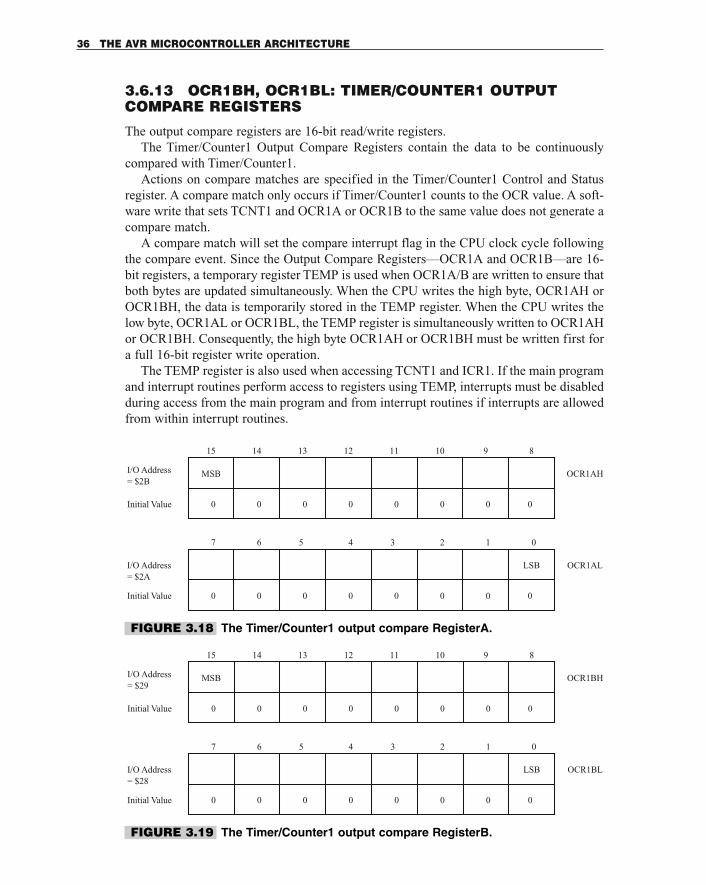
3.6.13 OCR1BH, OCR1BL: TIMER/COUNTER1 OUTPUTCOMPARE REGISTERS
The output compare registers are 16-bit read/write registers.The Timer/Counter1 Output Compare Registers contain the data to be continuously
compared with Timer/Counter1.Actions on compare matches are specified in the Timer/Counter1 Control and Status
register. A compare match only occurs if Timer/Counter1 counts to the OCR value. A soft-ware write that sets TCNT1 and OCR1A or OCR1B to the same value does not generate acompare match.
A compare match will set the compare interrupt flag in the CPU clock cycle followingthe compare event. Since the Output Compare Registers—OCR1A and OCR1B—are 16-bit registers, a temporary register TEMP is used when OCR1A/B are written to ensure thatboth bytes are updated simultaneously. When the CPU writes the high byte, OCR1AH orOCR1BH, the data is temporarily stored in the TEMP register. When the CPU writes thelow byte, OCR1AL or OCR1BL, the TEMP register is simultaneously written to OCR1AHor OCR1BH. Consequently, the high byte OCR1AH or OCR1BH must be written first fora full 16-bit register write operation.
The TEMP register is also used when accessing TCNT1 and ICR1. If the main programand interrupt routines perform access to registers using TEMP, interrupts must be disabledduring access from the main program and from interrupt routines if interrupts are allowedfrom within interrupt routines.
36 THE AVR MICROCONTROLLER ARCHITECTURE
01234567
I/O Address
Initial Value 0 0 0 0 0 0 0 0
MSB
15 14 13 12 11 10 9 8
= $2B
I/O Address
Initial Value 0 0 0 0 0 0 0 0
LSB= $2A
OCR1AH
OCR1AL
01234567
I/O Address
Initial Value 0 0 0 0 0 0 0 0
MSB
15 14 13 12 11 10 9 8
I/O Address
Initial Value 0 0 0 0 0 0 0 0
LSB
= $29
= $28
OCR1BH
OCR1BL
FIGURE 3.18 The Timer/Counter1 output compare RegisterA.
FIGURE 3.19 The Timer/Counter1 output compare RegisterB.
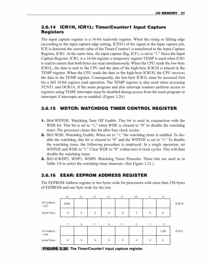
3.6.14 ICR1H, ICR1L: Timer/Counter1 Input CaptureRegisters
The input capture register is a 16-bit read-only register. When the rising or falling edge(according to the input capture edge setting, ICES1) of the signal at the input capture pin,ICP, is detected, the current value of the Timer/Counter1 is transferred to the Input CaptureRegister, ICR1. At the same time, the input capture flag, ICF1, is set to “1.” Since the InputCapture Register, ICR1, is a 16-bit register, a temporary register TEMP is used when ICR1is read to ensure that both bytes are read simultaneously. When the CPU reads the low-byteICR1L, the data is sent to the CPU and the data of the high-byte ICR1H is placed in theTEMP register. When the CPU reads the data in the high-byte ICR1H, the CPU receivesthe data in the TEMP register. Consequently, the low-byte ICR1L must be accessed firstfor a full 16-bit register read operation. The TEMP register is also used when accessingTCNT1 and OCR1A. If the main program and also interrupt routines perform access toregisters using TEMP, interrupts must be disabled during access from the main program orinterrupts if interrupts are re-enabled. (Figure 3.20.)
3.6.15 WDTCR: WATCHDOG TIMER CONTROL REGISTER
1. Bit4:WDTOE. Watchdog Turn Off Enable. This bit is used in conjunction with theWDE bit. This bit is set to “1,” when WDE is cleared to “0” to disable the watchdogtimer. The processor clears this bit after four clock cycles.
2. Bit3:WDE. Watchdog Enable. When set to “1,” the watchdog timer is enabled. To dis-able the watchdog, this bit is cleared to “0” and the WDTOE is set to “1.” To disablethe watchdog timer, the following procedure is employed: In a single operation, setWDTOE and WDE to “1.” Clear WDE to “0” within next 4 clock cycles. This will thendisable the watchdog timer.
3. Bit2-0:WDP2, WDP1, WDP0. Watchdog Timer Prescaler. These bits are used as inTable 3.8 to select the watchdog timer timeouts. (See Figure 3.21.)
3.6.16 EEAR: EEPROM ADDRESS REGISTER
The EEPROM Address register is two bytes wide for processors with more than 256 bytesof EEPROM and one byte wide for the rest.
I/O MEMORY 37
01234567
I/O Address
Initial Value 0 0 0 0 0 0 0 0
MSB
15 14 13 12 11 10 9 8
I/O Address
Initial Value 0 0 0 0 0 0 0 0
LSB
= $25
= $24
ICR1H
ICR1L
FIGURE 3.20 The Timer/Counter1 input capture register.
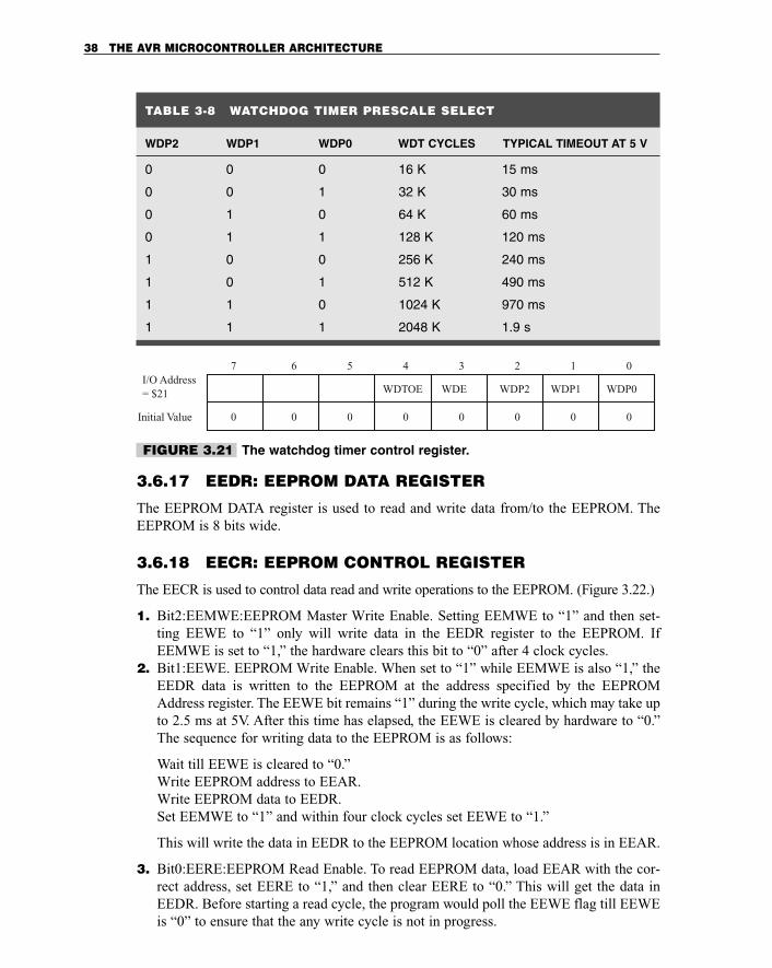
3.6.17 EEDR: EEPROM DATA REGISTER
The EEPROM DATA register is used to read and write data from/to the EEPROM. TheEEPROM is 8 bits wide.
3.6.18 EECR: EEPROM CONTROL REGISTER
The EECR is used to control data read and write operations to the EEPROM. (Figure 3.22.)
1. Bit2:EEMWE:EEPROM Master Write Enable. Setting EEMWE to “1” and then set-ting EEWE to “1” only will write data in the EEDR register to the EEPROM. IfEEMWE is set to “1,” the hardware clears this bit to “0” after 4 clock cycles.
2. Bit1:EEWE. EEPROM Write Enable. When set to “1” while EEMWE is also “1,” theEEDR data is written to the EEPROM at the address specified by the EEPROMAddress register. The EEWE bit remains “1” during the write cycle, which may take upto 2.5 ms at 5V. After this time has elapsed, the EEWE is cleared by hardware to “0.”The sequence for writing data to the EEPROM is as follows:
Wait till EEWE is cleared to “0.”Write EEPROM address to EEAR.Write EEPROM data to EEDR.Set EEMWE to “1” and within four clock cycles set EEWE to “1.”
This will write the data in EEDR to the EEPROM location whose address is in EEAR.
3. Bit0:EERE:EEPROM Read Enable. To read EEPROM data, load EEAR with the cor-rect address, set EERE to “1,” and then clear EERE to “0.” This will get the data inEEDR. Before starting a read cycle, the program would poll the EEWE flag till EEWEis “0” to ensure that the any write cycle is not in progress.
38 THE AVR MICROCONTROLLER ARCHITECTURE
Initial Value
I/O Address
0 0 0 0 0 0 0 0
7 6 5 4 3 2 1 0
= $21 WDTOE WDE WDP2 WDP1 WDP0
FIGURE 3.21 The watchdog timer control register.
TABLE 3-8 WATCHDOG TIMER PRESCALE SELECT
WDP2 WDP1 WDP0 WDT CYCLES TYPICAL TIMEOUT AT 5 V
0 0 0 16 K 15 ms
0 0 1 32 K 30 ms
0 1 0 64 K 60 ms
0 1 1 128 K 120 ms
1 0 0 256 K 240 ms
1 0 1 512 K 490 ms
1 1 0 1024 K 970 ms
1 1 1 2048 K 1.9 s
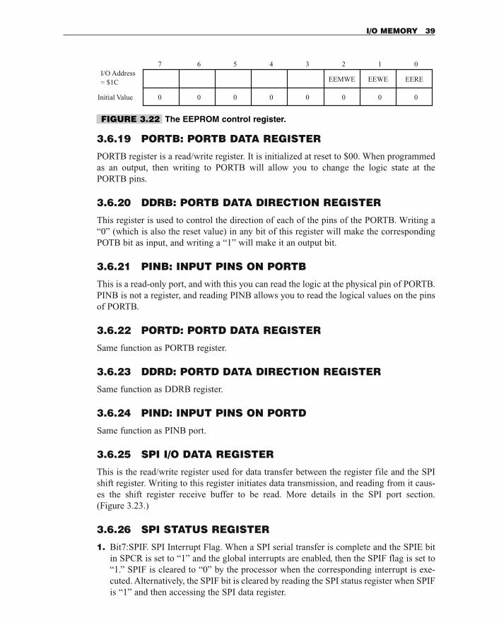
3.6.19 PORTB: PORTB DATA REGISTER
PORTB register is a read/write register. It is initialized at reset to $00. When programmedas an output, then writing to PORTB will allow you to change the logic state at the PORTB pins.
3.6.20 DDRB: PORTB DATA DIRECTION REGISTER
This register is used to control the direction of each of the pins of the PORTB. Writing a“0” (which is also the reset value) in any bit of this register will make the correspondingPOTB bit as input, and writing a “1” will make it an output bit.
3.6.21 PINB: INPUT PINS ON PORTB
This is a read-only port, and with this you can read the logic at the physical pin of PORTB.PINB is not a register, and reading PINB allows you to read the logical values on the pinsof PORTB.
3.6.22 PORTD: PORTD DATA REGISTER
Same function as PORTB register.
3.6.23 DDRD: PORTD DATA DIRECTION REGISTER
Same function as DDRB register.
3.6.24 PIND: INPUT PINS ON PORTD
Same function as PINB port.
3.6.25 SPI I/O DATA REGISTER
This is the read/write register used for data transfer between the register file and the SPIshift register. Writing to this register initiates data transmission, and reading from it caus-es the shift register receive buffer to be read. More details in the SPI port section. (Figure 3.23.)
3.6.26 SPI STATUS REGISTER
1. Bit7:SPIF. SPI Interrupt Flag. When a SPI serial transfer is complete and the SPIE bitin SPCR is set to “1” and the global interrupts are enabled, then the SPIF flag is set to“1.” SPIF is cleared to “0” by the processor when the corresponding interrupt is exe-cuted. Alternatively, the SPIF bit is cleared by reading the SPI status register when SPIFis “1” and then accessing the SPI data register.
I/O MEMORY 39
Initial Value
I/O Address
0 0 0 0 0 0 0 0
7 6 5 4 3 2 1 0
= $1C EEMWE EEWE EERE
FIGURE 3.22 The EEPROM control register.
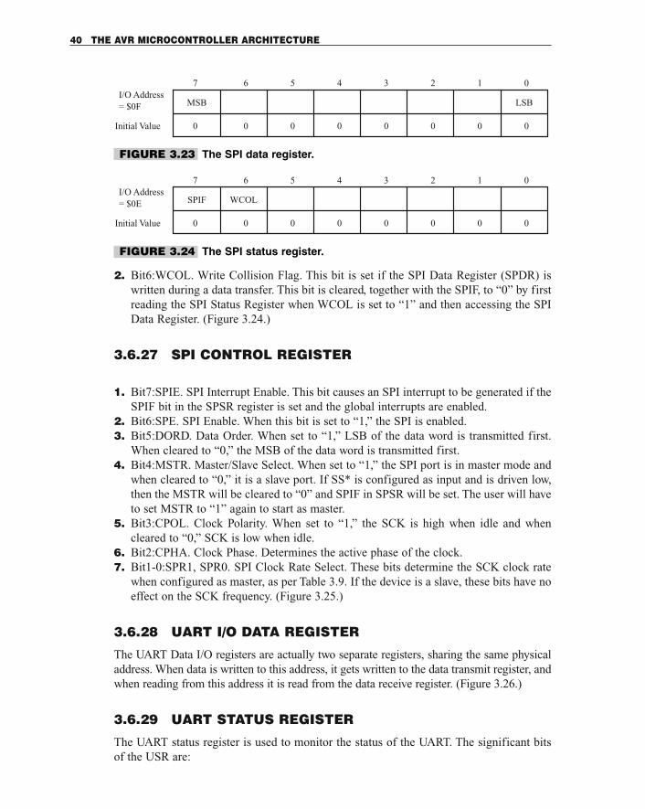
2. Bit6:WCOL. Write Collision Flag. This bit is set if the SPI Data Register (SPDR) iswritten during a data transfer. This bit is cleared, together with the SPIF, to “0” by firstreading the SPI Status Register when WCOL is set to “1” and then accessing the SPIData Register. (Figure 3.24.)
3.6.27 SPI CONTROL REGISTER
1. Bit7:SPIE. SPI Interrupt Enable. This bit causes an SPI interrupt to be generated if theSPIF bit in the SPSR register is set and the global interrupts are enabled.
2. Bit6:SPE. SPI Enable. When this bit is set to “1,” the SPI is enabled.3. Bit5:DORD. Data Order. When set to “1,” LSB of the data word is transmitted first.
When cleared to “0,” the MSB of the data word is transmitted first.4. Bit4:MSTR. Master/Slave Select. When set to “1,” the SPI port is in master mode and
when cleared to “0,” it is a slave port. If SS* is configured as input and is driven low,then the MSTR will be cleared to “0” and SPIF in SPSR will be set. The user will haveto set MSTR to “1” again to start as master.
5. Bit3:CPOL. Clock Polarity. When set to “1,” the SCK is high when idle and whencleared to “0,” SCK is low when idle.
6. Bit2:CPHA. Clock Phase. Determines the active phase of the clock.7. Bit1-0:SPR1, SPR0. SPI Clock Rate Select. These bits determine the SCK clock rate
when configured as master, as per Table 3.9. If the device is a slave, these bits have noeffect on the SCK frequency. (Figure 3.25.)
3.6.28 UART I/O DATA REGISTER
The UART Data I/O registers are actually two separate registers, sharing the same physicaladdress. When data is written to this address, it gets written to the data transmit register, andwhen reading from this address it is read from the data receive register. (Figure 3.26.)
3.6.29 UART STATUS REGISTER
The UART status register is used to monitor the status of the UART. The significant bitsof the USR are:
40 THE AVR MICROCONTROLLER ARCHITECTURE
Initial Value
I/O Address
0 0 0 0 0 0 0 0
7 6 5 4 3 2 1 0
= $0F MSB LSB
Initial Value
I/O Address
0 0 0 0 0 0 0 0
7 6 5 4 3 2 1 0
= $0E SPIF WCOL
FIGURE 3.23 The SPI data register.
FIGURE 3.24 The SPI status register.
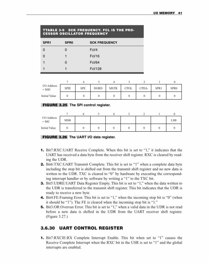
1. Bit7:RXC:UART Receive Complete. When this bit is set to “1,” it indicates that theUART has received a data byte from the receiver shift register. RXC is cleared by read-ing the UDR.
2. Bit6:TXC:UART Transmit Complete. This bit is set to “1” when a complete data byteincluding the stop bit is shifted out from the transmit shift register and no new data iswritten to the UDR. TXC is cleared to “0” by hardware by executing the correspond-ing interrupt handler or by software by writing a “1” to the TXC bit.
3. Bit5:UDRE:UART Data Register Empty. This bit is set to “1,” when the data written tothe UDR is transferred to the transmit shift register. This bit indicates that the UDR isready to receive a new byte.
4. Bit4:FE:Framing Error. This bit is set to “1,” when the incoming stop bit is “0” (whenit should be “1”). The FE is cleared when the incoming stop bit is “1.”
5. Bit3:OR:Overrun Error. This bit is set to “1,” when a valid data in the UDR is not readbefore a new data is shifted in the UDR from the UART receiver shift register. (Figure 3.27.)
3.6.30 UART CONTROL REGISTER
1. Bit7:RXCIE:RX Complete Interrupt Enable. This bit when set to “1” causes theReceive Complete Interrupt when the RXC bit in the USR is set to “1” and the globalinterrupts are enabled.
I/O MEMORY 41
TTABLE 3-9 SCK FREQUENCY. FCL IS THE PRO-CESSOR OSCILLATOR FREQUENCY
SPR1 SPR0 SCK FREQUENCY
0 0 Fcl/4
0 1 Fcl/16
1 0 Fcl/64
1 1 Fcl/128
Initial Value
I/O Address
0 0 0 0 0 0 0 0
7 6 5 4 3 2 1 0
= $0D SPIE SPE DORD MSTR CPOL CPHA SPR1 SPR0
FIGURE 3.25 The SPI control register.
Initial Value
I/O Address
0 0 0 0 0 0 0 0
7 6 5 4 3 2 1 0
MSB LSB= $0C
FIGURE 3.26 The UART I/O data register.
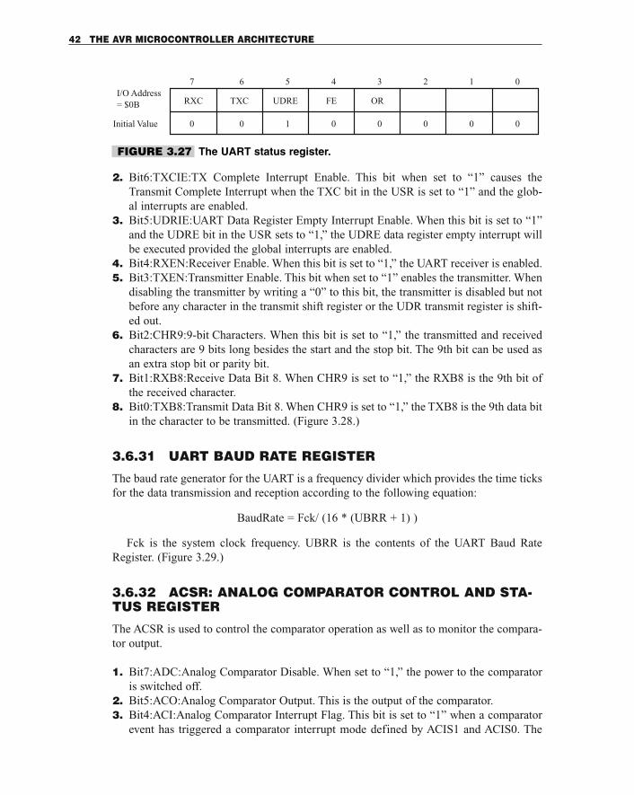
2. Bit6:TXCIE:TX Complete Interrupt Enable. This bit when set to “1” causes theTransmit Complete Interrupt when the TXC bit in the USR is set to “1” and the glob-al interrupts are enabled.
3. Bit5:UDRIE:UART Data Register Empty Interrupt Enable. When this bit is set to “1”and the UDRE bit in the USR sets to “1,” the UDRE data register empty interrupt willbe executed provided the global interrupts are enabled.
4. Bit4:RXEN:Receiver Enable. When this bit is set to “1,” the UART receiver is enabled.5. Bit3:TXEN:Transmitter Enable. This bit when set to “1” enables the transmitter. When
disabling the transmitter by writing a “0” to this bit, the transmitter is disabled but notbefore any character in the transmit shift register or the UDR transmit register is shift-ed out.
6. Bit2:CHR9:9-bit Characters. When this bit is set to “1,” the transmitted and receivedcharacters are 9 bits long besides the start and the stop bit. The 9th bit can be used asan extra stop bit or parity bit.
7. Bit1:RXB8:Receive Data Bit 8. When CHR9 is set to “1,” the RXB8 is the 9th bit ofthe received character.
8. Bit0:TXB8:Transmit Data Bit 8. When CHR9 is set to “1,” the TXB8 is the 9th data bitin the character to be transmitted. (Figure 3.28.)
3.6.31 UART BAUD RATE REGISTER
The baud rate generator for the UART is a frequency divider which provides the time ticksfor the data transmission and reception according to the following equation:
BaudRate = Fck/ (16 * (UBRR + 1) )
Fck is the system clock frequency. UBRR is the contents of the UART Baud RateRegister. (Figure 3.29.)
3.6.32 ACSR: ANALOG COMPARATOR CONTROL AND STA-TUS REGISTER
The ACSR is used to control the comparator operation as well as to monitor the compara-tor output.
1. Bit7:ADC:Analog Comparator Disable. When set to “1,” the power to the comparatoris switched off.
2. Bit5:ACO:Analog Comparator Output. This is the output of the comparator.3. Bit4:ACI:Analog Comparator Interrupt Flag. This bit is set to “1” when a comparator
event has triggered a comparator interrupt mode defined by ACIS1 and ACIS0. The
42 THE AVR MICROCONTROLLER ARCHITECTURE
Initial Value
I/O Address
0 0 0 0 0 0 0
7 6 5 4 3 2 1 0
= $0B RXC TXC UDRE FE OR
1
FIGURE 3.27 The UART status register.
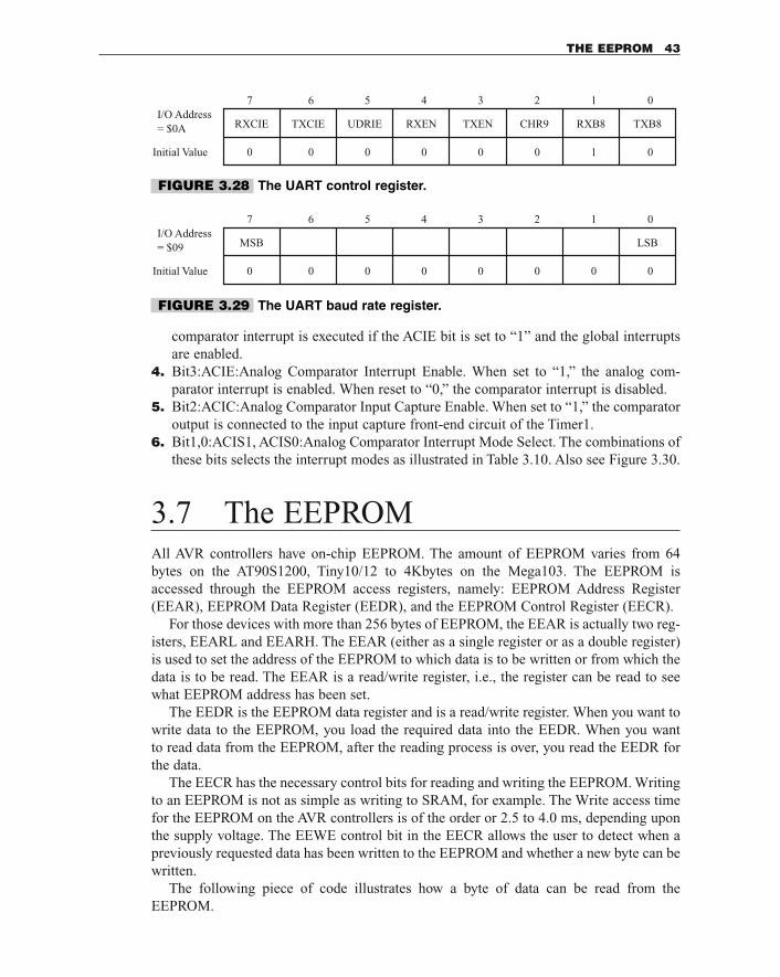
comparator interrupt is executed if the ACIE bit is set to “1” and the global interruptsare enabled.
4. Bit3:ACIE:Analog Comparator Interrupt Enable. When set to “1,” the analog com-parator interrupt is enabled. When reset to “0,” the comparator interrupt is disabled.
5. Bit2:ACIC:Analog Comparator Input Capture Enable. When set to “1,” the comparatoroutput is connected to the input capture front-end circuit of the Timer1.
6. Bit1,0:ACIS1, ACIS0:Analog Comparator Interrupt Mode Select. The combinations ofthese bits selects the interrupt modes as illustrated in Table 3.10. Also see Figure 3.30.
3.7 The EEPROMAll AVR controllers have on-chip EEPROM. The amount of EEPROM varies from 64bytes on the AT90S1200, Tiny10/12 to 4Kbytes on the Mega103. The EEPROM isaccessed through the EEPROM access registers, namely: EEPROM Address Register(EEAR), EEPROM Data Register (EEDR), and the EEPROM Control Register (EECR).
For those devices with more than 256 bytes of EEPROM, the EEAR is actually two reg-isters, EEARL and EEARH. The EEAR (either as a single register or as a double register)is used to set the address of the EEPROM to which data is to be written or from which thedata is to be read. The EEAR is a read/write register, i.e., the register can be read to seewhat EEPROM address has been set.
The EEDR is the EEPROM data register and is a read/write register. When you want towrite data to the EEPROM, you load the required data into the EEDR. When you want to read data from the EEPROM, after the reading process is over, you read the EEDR for the data.
The EECR has the necessary control bits for reading and writing the EEPROM. Writingto an EEPROM is not as simple as writing to SRAM, for example. The Write access timefor the EEPROM on the AVR controllers is of the order or 2.5 to 4.0 ms, depending uponthe supply voltage. The EEWE control bit in the EECR allows the user to detect when apreviously requested data has been written to the EEPROM and whether a new byte can bewritten.
The following piece of code illustrates how a byte of data can be read from the EEPROM.
THE EEPROM 43
Initial Value
I/O Address
0 0 0 0 0 0
7 6 5 4 3 2 1 0
= $0A RXCIE TXCIE UDRIE RXEN TXEN CHR9 RXB8 TXB8
10
FIGURE 3.28 The UART control register.
Initial Value
I/O Address
0 0 0 0 0 0
7 6 5 4 3 2 1 0
= $09
0 0
MSB LSB
FIGURE 3.29 The UART baud rate register.
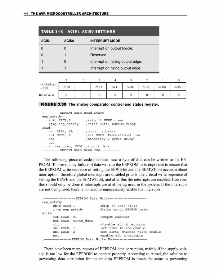
;———————-EEPROM Data Read Start—————————eep_notrdy:
sbic EECR,1 ;skip if EEWE clearrjmp eep_notrdy ;Waits until EEPROM ready
read:out EEAR, ZL ;output addresssbi EECR, 0 ;set EERE (Read-strobe) lownop ;mandatory 2 cycle delaynopin read_reg, EEDR ;inputs data
;———————-EEPROM Data Read End—————————-
The following piece of code illustrates how a byte of data can be written to the EE-PROM. To prevent any failure of data write to the EEPROM, it is important to ensure thatthe EEPROM write sequence of setting the EEWE bit and the EEMWE bit occurs withoutinterruption; therefore global interrupts are disabled prior to the critical write sequence ofsetting the EEWE and the EEMWE bit, and after this the interrupts are enabled. However,this should only be done if interrupts are at all being used in the system. If the interruptsare not being used, there is no need to unnecessarily enable the interrupts.
;———————-—-—-—-—-EEPROM Data Write—-—-——-—-—————————-eep_notrdy:
sbic EECR,1 ;skip if EEWE clearrjmp eep_notrdy ;Waits until EEPROM ready
write:out EEAR, ZL ;output addressout EEDR, write_datacli ;disable all interruptssbi EECR, 1 ;set EEWE (Write-enable) sbi EECR, 2 ;set EEMWE (Master Write-enable)sei ;enable all interrupts
;———————-—-—-—-EEPROM Data Write End——-—-—-—————————-
There have been many reports of EEPROM data corruption, mainly if the supply volt-age is too low for the EEPROM to operate properly. According to Atmel, the solution topreventing data corruption for the on-chip EEPROM is much the same as preventing
44 THE AVR MICROCONTROLLER ARCHITECTURE
Initial Value
I/O Address
0 0 0 0 0 0
7 6 5 4 3 2 1 0
0
= $08 ACD ACO ACI ACIE ACIC ACIS1 ACIS0
0
FIGURE 3.30 The analog comparator control and status register.
TABLE 3-10 ACIS1, ACIS0 SETTINGS
ACIS1 ACIS0 INTERRUPT MODE
0 0 Interrupt on output toggle.
0 1 Reserved.
1 0 Interrupt on falling output edge.
1 1 Interrupt on rising output edge.
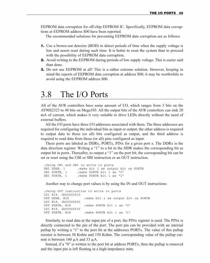
EEPROM data corruption for off-chip EEPROM IC. Specifically, EEPROM data corrup-tions at EEPROM address $00 have been reported.
The recommended solutions for preventing EEPROM date corruption are as follows:
1. Use a brown-out detector (BOD) to detect periods of time when the supply voltage islow and assert reset during such time. It is better to reset the system than to proceedwith the possibility of EEPROM data corruption.
2. Avoid writing to the EEPROM during periods of low supply voltage. This is easier saidthan done.
3. Do not use EEPROM at all! This is a rather extreme solution. However, keeping inmind the reports of EEPROM data corruption at address $00, it may be worthwhile toavoid using the EEPROM address $00.
3.8 The I/O PortsAll of the AVR controllers have some amount of I/O, which ranges from 3 bits on theAT90S2323 to 48 bits on Mega103. All the output bits of the AVR controllers can sink 20mA of current, which makes it very suitable to drive LEDs directly without the need ofexternal buffers.
All the I/O ports have three I/O addresses associated with them. The three addresses arerequired for configuring the individual bits as input or output; the other address is requiredto output data to those (or all) bits configured as output, and the third address is required to read data from those (or all) pins configured as input.
These ports are labeled as DDRx, PORTx, PINx for a given port x. The DDRx is thedata direction register. Writing a “1” to a bit in the DDR makes the corresponding bit asoutput bit in portx. Thereafter, to output a “1” on the port bit, the corresponding bit can beset or reset using the CBI or SBI instruction or an OUT instruction.
;Using CBI and SBI to write to portsSBI DDRB, 1 ;make bit 1 as output bit on PORTBCBI PORTB, 1 ;make PORTB bit 1 as “0”SBI PORTB, 1 ;make PORTB bit 1 as “1”
Another way to change port values is by using the IN and OUT instructions:
;Using OUT instruction to write to portsLDI R18, 0b00000010OUT DDRB, R18 ;make bit 1 as output bit on PORTBLDI R18, 0b00000000OUT PORTB, R18 ;make PORTB bit 1 as “0”LDI R18, 0b00000010OUT PORTB, R18 ;make PORTB bit 1 as “1”
Similarly, to read data at the input pin of a port, the PINx register is used. The PINx isdirectly connected to the pin of the port. The port pin can be provided with an internalpullup by writing a “1” to the port bit at the addresses PORTx. The value of this pullupresistor is between 30 Kohm and 150 Kohm. The corresponding value of the pullup cur-rent is between 160 �A and 33 �A.
Instead, if a “0” is written to the port bit at address PORTx, then the pullup is removedand the input pin is left floating in a high-impedance state.
THE I/O PORTS 45
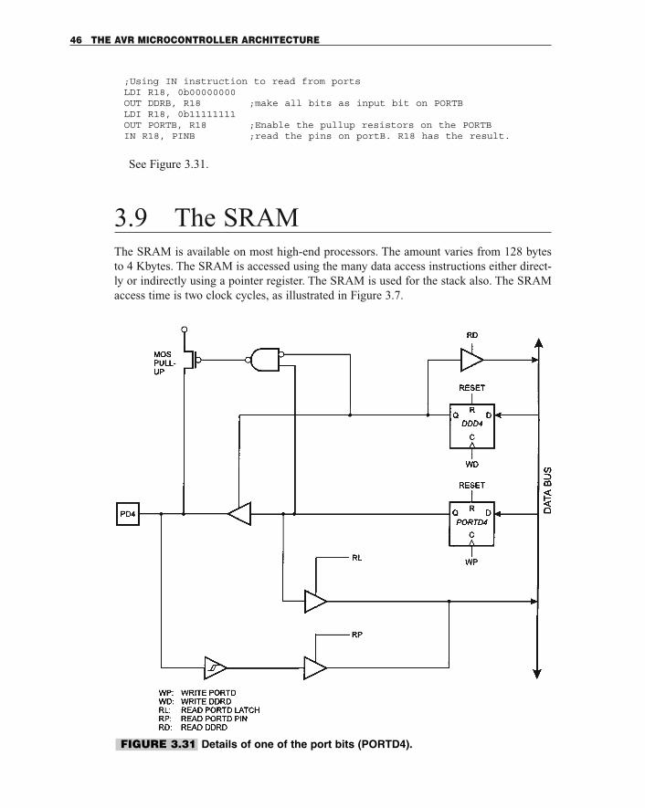
;Using IN instruction to read from portsLDI R18, 0b00000000OUT DDRB, R18 ;make all bits as input bit on PORTBLDI R18, 0b11111111OUT PORTB, R18 ;Enable the pullup resistors on the PORTBIN R18, PINB ;read the pins on portB. R18 has the result.
See Figure 3.31.
3.9 The SRAMThe SRAM is available on most high-end processors. The amount varies from 128 bytesto 4 Kbytes. The SRAM is accessed using the many data access instructions either direct-ly or indirectly using a pointer register. The SRAM is used for the stack also. The SRAMaccess time is two clock cycles, as illustrated in Figure 3.7.
46 THE AVR MICROCONTROLLER ARCHITECTURE
FIGURE 3.31 Details of one of the port bits (PORTD4).
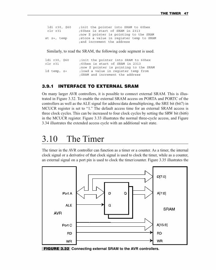
ldi r30, $60 ;init the pointer into SRAM to 60hexclr r31 ;60hex is start of SRAM in 2313
;now Z pointer is pointing to the SRAMst z+, temp ;store a value in register temp to SRAM
;and increment the address
Similarly, to read the SRAM, the following code segment is used.
ldi r30, $60 ;init the pointer into SRAM to 60hexclr r31 ;60hex is start of SRAM in 2313
;now Z pointer is pointing to the SRAMld temp, z+ ;load a value in register temp from
;SRAM and increment the address
3.9.1 INTERFACE TO EXTERNAL SRAM
On many larger AVR controllers, it is possible to connect external SRAM. This is illus-trated in Figure 3.32. To enable the external SRAM access on PORTA and PORTC of thecontrollers as well as the ALE signal for address/data demultiplexing, the SRE bit (bit7) inMCUCR register is set to “1.” The default access time for an external SRAM access isthree clock cycles. This can be increased to four clock cycles by setting the SRW bit (bit6)in the MCUCR register. Figure 3.33 illustrates the normal three-cycle access, and Figure3.34 illustrates the extended access cycle with an additional wait state.
3.10 The TimerThe timer in the AVR controller can function as a timer or a counter. As a timer, the internalclock signal or a derivative of that clock signal is used to clock the timer, while as a counter,an external signal on a port pin is used to clock the timer/counter. Figure 3.35 illustrates the
THE TIMER 47
FIGURE 3.32 Connecting external SRAM to the AVR controllers.
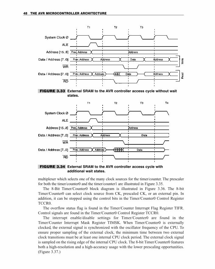
multiplexer which selects one of the many clock sources for the timer/counter. The prescalerfor both the timer/counter0 and the timer/counter1 are illustrated in Figure 3.35.
The 8-Bit Timer/Counter0 block diagram is illustrated in Figure 3.36. The 8-bitTimer/Counter0 can select clock source from CK, prescaled CK, or an external pin. Inaddition, it can be stopped using the control bits in the Timer/Counter0 Control RegisterTCCR0.
The overflow status flag is found in the Timer/Counter Interrupt Flag Register TIFR.Control signals are found in the Timer/Counter0 Control Register TCCR0.
The interrupt enable/disable settings for Timer/Counter0 are found in theTimer/Counter Interrupt Mask Register TIMSK. When Timer/Counter0 is externallyclocked, the external signal is synchronized with the oscillator frequency of the CPU. Toensure proper sampling of the external clock, the minimum time between two externalclock transitions must be at least one internal CPU clock period. The external clock signalis sampled on the rising edge of the internal CPU clock. The 8-bit Timer/Counter0 featuresboth a high-resolution and a high-accuracy usage with the lower prescaling opportunities.(Figure 3.37.)
48 THE AVR MICROCONTROLLER ARCHITECTURE
FIGURE 3.33 External SRAM to the AVR controller access cycle without waitstates.
FIGURE 3.34 External SRAM to the AVR controller access cycle withadditional wait states.
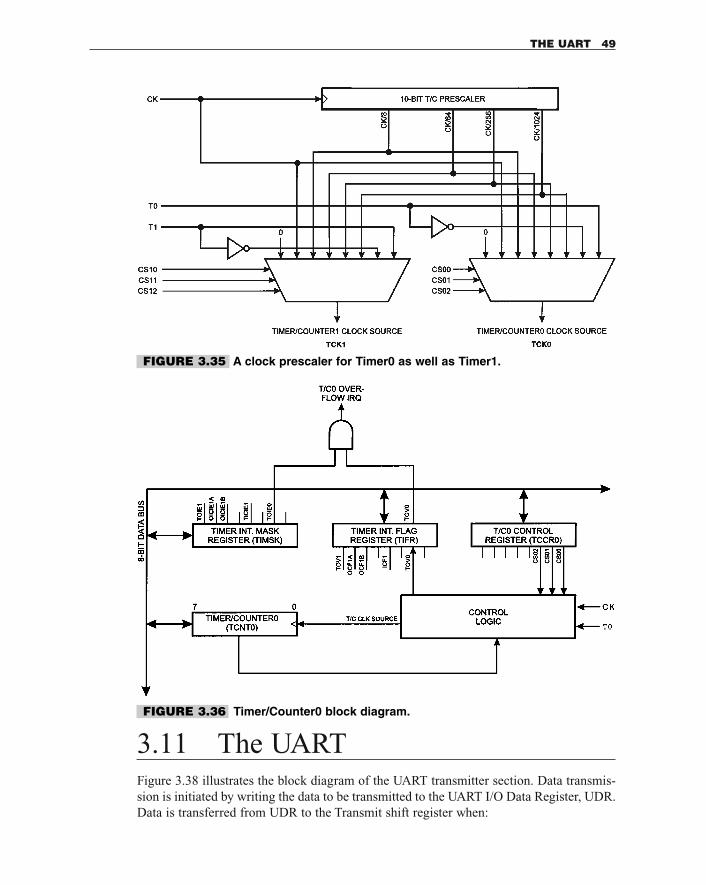
3.11 The UARTFigure 3.38 illustrates the block diagram of the UART transmitter section. Data transmis-sion is initiated by writing the data to be transmitted to the UART I/O Data Register, UDR.Data is transferred from UDR to the Transmit shift register when:
THE UART 49
FIGURE 3.35 A clock prescaler for Timer0 as well as Timer1.
FIGURE 3.36 Timer/Counter0 block diagram.
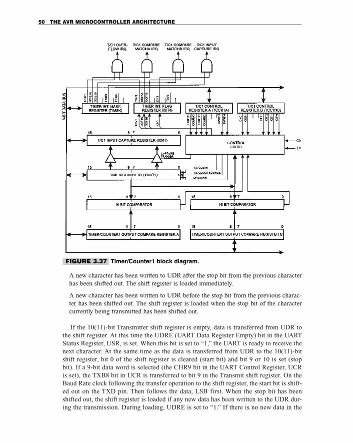
A new character has been written to UDR after the stop bit from the previous characterhas been shifted out. The shift register is loaded immediately.
A new character has been written to UDR before the stop bit from the previous charac-ter has been shifted out. The shift register is loaded when the stop bit of the charactercurrently being transmitted has been shifted out.
If the 10(11)-bit Transmitter shift register is empty, data is transferred from UDR tothe shift register. At this time the UDRE (UART Data Register Empty) bit in the UARTStatus Register, USR, is set. When this bit is set to “1,” the UART is ready to receive thenext character. At the same time as the data is transferred from UDR to the 10(11)-bitshift register, bit 0 of the shift register is cleared (start bit) and bit 9 or 10 is set (stopbit). If a 9-bit data word is selected (the CHR9 bit in the UART Control Register, UCRis set), the TXB8 bit in UCR is transferred to bit 9 in the Transmit shift register. On theBaud Rate clock following the transfer operation to the shift register, the start bit is shift-ed out on the TXD pin. Then follows the data, LSB first. When the stop bit has beenshifted out, the shift register is loaded if any new data has been written to the UDR dur-ing the transmission. During loading, UDRE is set to “1.” If there is no new data in the
50 THE AVR MICROCONTROLLER ARCHITECTURE
FIGURE 3.37 Timer/Counter1 block diagram.
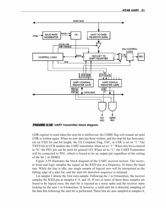
UDR register to send when the stop bit is shifted out, the UDRE flag will remain set untilUDR is written again. When no new data has been written, and the stop bit has been pres-ent on TXD for one bit length, the TX Complete Flag, TXC, in USR is set to “1.” TheTXEN bit in UCR enables the UART transmitter when set to “1.” When this bit is clearedto “0,” the PD1 pin can be used for general I/O. When set to “1,” the UART Transmitterwill be connected to PD1, which is forced to be an output pin regardless of the settingof the bit 1 in DDRD.
Figure 3.39 illustrates the block diagram of the UART receiver section. The receiv-er front-end logic samples the signal on the RXD pin at a frequency 16 times the baudrate. While the line is idle, one single sample of logical zero will be interpreted as thefalling edge of a start bit, and the start bit detection sequence is initiated.
Let sample 1 denote the first zero-sample. Following the 1 to 0-transition, the receiversamples the RXD pin at samples 8, 9, and 10. If two or more of these three samples arefound to be logical ones, the start bit is rejected as a noise spike and the receiver startslooking for the next 1 to 0-transition. If, however, a valid start bit is detected, sampling ofthe data bits following the start bit is performed. These bits are also sampled at samples 8,
HTHE UART 51
FIGURE 3.38 UART transmitter block diagram.
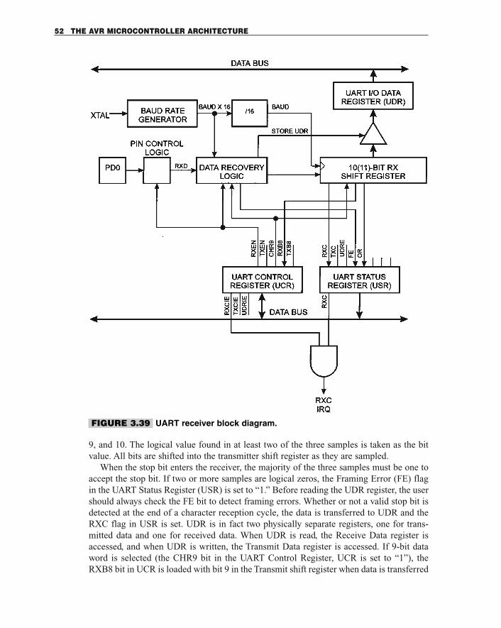
9, and 10. The logical value found in at least two of the three samples is taken as the bitvalue. All bits are shifted into the transmitter shift register as they are sampled.
When the stop bit enters the receiver, the majority of the three samples must be one toaccept the stop bit. If two or more samples are logical zeros, the Framing Error (FE) flagin the UART Status Register (USR) is set to “1.” Before reading the UDR register, the usershould always check the FE bit to detect framing errors. Whether or not a valid stop bit isdetected at the end of a character reception cycle, the data is transferred to UDR and theRXC flag in USR is set. UDR is in fact two physically separate registers, one for trans-mitted data and one for received data. When UDR is read, the Receive Data register isaccessed, and when UDR is written, the Transmit Data register is accessed. If 9-bit dataword is selected (the CHR9 bit in the UART Control Register, UCR is set to “1”), theRXB8 bit in UCR is loaded with bit 9 in the Transmit shift register when data is transferred
52 THE AVR MICROCONTROLLER ARCHITECTURE
FIGURE 3.39 UART receiver block diagram.
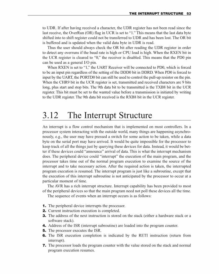
to UDR. If after having received a character, the UDR register has not been read since thelast receive, the OverRun (OR) flag in UCR is set to “1.” This means that the last data byteshifted into to shift register could not be transferred to UDR and has been lost. The OR bitis buffered and is updated when the valid data byte in UDR is read.
Thus the user should always check the OR bit after reading the UDR register in orderto detect any overruns if the baud rate is high or CPU load is high. When the RXEN bit inthe UCR register is cleared to “0,” the receiver is disabled. This means that the PD0 pincan be used as a general I/O pin.
When RXEN is set to “1,” the UART Receiver will be connected to PD0, which is forcedto be an input pin regardless of the setting of the DDD0 bit in DDRD. When PD0 is forced toinput by the UART, the PORTD0 bit can still be used to control the pull-up resistor on the pin.When the CHR9 bit in the UCR register is set, transmitted and received characters are 9 bitslong, plus start and stop bits. The 9th data bit to be transmitted is the TXB8 bit in the UCRregister. This bit must be set to the wanted value before a transmission is initiated by writingto the UDR register. The 9th data bit received is the RXB8 bit in the UCR register.
3.12 The Interrupt StructureAn interrupt is a flow control mechanism that is implemented on most controllers. In aprocessor system interacting with the outside world, many things are happening asynchro-nously, e.g., the user may have pressed a switch for some action to be taken, while a databyte on the serial port may have arrived. It would be quite impossible for the processor tokeep track of all the things just by querying these devices for data. Instead, it would be bet-ter if these devices could “announce” arrival of data. This is what the interrupt mechanismdoes. The peripheral device could “interrupt” the execution of the main program, and theprocessor takes time out of the normal program execution to examine the source of theinterrupt and to take necessary action. After the required action is taken, the interruptedprogram execution is resumed. The interrupt program is just like a subroutine, except thatthe execution of this interrupt subroutine is not anticipated by the processor to occur at aparticular moment of time.
The AVR has a rich interrupt structure. Interrupt capability has been provided to mostof the peripheral devices so that the main program need not poll these devices all the time.
The sequence of events when an interrupt occurs is as follows:
1. The peripheral device interrupts the processor.2. Current instruction execution is completed.3. The address of the next instruction is stored on the stack (either a hardware stack or a
software stack).4. Address of the ISR (interrupt subroutine) are loaded into the program counter.5. The processor executes the ISR.6. The ISR execution completion is indicated by the RETI instruction (return from
interrupt).7. The processor loads the program counter with the value stored on the stack and normal
program execution resumes.
THE INTERRUPT STRUCTURE 53
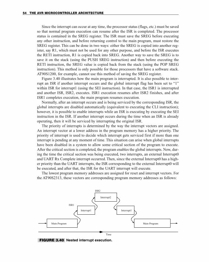
Since the interrupt can occur at any time, the processor status (flags, etc.) must be savedso that normal program execution can resume after the ISR is completed. The processorstatus is contained in the SREG register. The ISR must save the SREG before executingany other instruction, and before returning control to the main program, must restore theSREG register. This can be done in two ways: either the SREG is copied into another reg-ister, say R1, which must not be used for any other purpose, and before the ISR executesthe RETI instruction, R1 is copied back into SREG. Another way to save the SREG is tosave it on the stack (using the PUSH SREG instruction) and then before executing theRETI instruction, the SREG value is copied back from the stack (using the POP SREGinstruction). This method is only possible for those processors that have a software stack.AT90S1200, for example, cannot use this method of saving the SREG register.
Figure 3.40 illustrates how the main program is interrupted. It is also possible to inter-rupt an ISR if another interrupt occurs and the global interrupt flag has been set to “1”within ISR for interrupt1 (using the SEI instruction). In that case, the ISR1 is interruptedand another ISR, ISR2, executes. ISR1 execution resumes after ISR2 finishes, and afterISR1 completes execution, the main program resumes execution.
Normally, after an interrupt occurs and is being serviced by the corresponding ISR, theglobal interrupts are disabled automatically (equivalent to executing the CLI instruction);however, it is possible to enable interrupts while an ISR is executing by executing the SEIinstruction in the ISR. If another interrupt occurs during the time when an ISR is alreadyoperating, then it will be serviced by interrupting the original ISR.
The priority of interrupts is determined by the way the interrupt vectors are assigned.An interrupt vector at a lower address in the program memory has a higher priority. Thepriority of interrupt is used to decide which interrupt gets serviced first if more than oneinterrupt is pending at any moment of time. This situation can arise when global interruptshave been disabled in a system to allow some critical section of the program to execute.After the critical section is completed, the program enables the global interrupts. Now, dur-ing the time the critical section was being executed, two interrupts, an external Interrupt0and UART Rx Complete interrupt occurred. Then, since the external Interrupt0 has a high-er priority than the UART interrupts, the ISR corresponding to the external Interrupt0 willbe executed, and after that, the ISR for the UART interrupt will execute.
The lowest program memory addresses are assigned for reset and interrupt vectors. Forthe AT90S2313, these vectors are corresponding program memory addresses as follows:
54 THE AVR MICROCONTROLLER ARCHITECTURE
Main Program
Interrupt1
Interrupt2
Interrupt1
Main Program
Time
ISR1
ISR2
FIGURE 3.40 Nested interrupt execution.
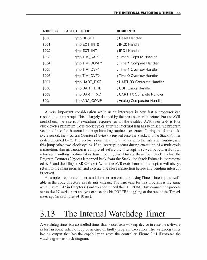
A very important consideration while using interrupts is how fast a processor canrespond to an interrupt. This is largely decided by the processor architecture. For the AVRcontrollers, the interrupt execution response for all the enabled AVR interrupts is fourclock cycles minimum. Four clock cycles after the interrupt flag has been set, the programvector address for the actual interrupt handling routine is executed. During this four-clock-cycle period, the Program Counter (2 bytes) is pushed onto the Stack, and the Stack Pointeris decremented by 2. The vector is normally a relative jump to the interrupt routine, andthis jump takes two clock cycles. If an interrupt occurs during execution of a multicycleinstruction, this instruction is completed before the interrupt is served. A return from aninterrupt handling routine takes four clock cycles. During these four clock cycles, theProgram Counter (2 bytes) is popped back from the Stack, the Stack Pointer is increment-ed by 2, and the I flag in SREG is set. When the AVR exits from an interrupt, it will alwaysreturn to the main program and execute one more instruction before any pending interruptis served.
A sample program to understand the interrupt operation using Timer1 interrupt is avail-able in the code directory as file intr_ex.asm. The hardware for this program is the sameas in Figure 6.47 in Chapter 6 (and you don’t need the EEPROM). Just connect the proces-sor to the PC serial port and you can see the bit PORTB6 toggling at the rate of the Timer1interrupt (in multiples of 10 ms).
3.13 The Internal Watchdog TimerA watchdog timer is a controlled timer that is used as a wakeup device in case the softwareis lost in some infinite loop or in case of faulty program execution. The watchdog timerhas an output that has the capability to reset the controller. Figure 3.41 illustrates thewatchdog timer block diagram.
THE INTERNAL WATCHDOG TIMER 55
ADDRESS LABELS CODE COMMENTS
$000 rjmp RESET ; Reset Handler
$001 rjmp EXT_INT0 ; IRQ0 Handler
$002 rjmp EXT_INT1 ; IRQ1 Handler
$003 rjmp TIM_CAPT1 ; Timer1 Capture Handler
$004 rjmp TIM_COMP1 ; Timer1 Compare Handler
$005 rjmp TIM_OVF1 ; Timer1 Overflow Handler
$006 rjmp TIM_OVF0 ; Timer0 Overflow Handler
$007 rjmp UART_RXC ; UART RX Complete Handler
$008 rjmp UART_DRE ; UDR Empty Handler
$009 rjmp UART_TXC ; UART TX Complete Handler
$00a rjmp ANA_COMP ; Analog Comparator Handler
The watchdog timer is clocked from a separate on-chip RC oscillator. By controllingthe watchdog timer prescaler, the watchdog reset interval can be adjusted as illustrated inTable 3.8. The watchdog reset intervals are also power-supply dependent.
The watchdog reset instruction, WDR, resets the watchdog timer. Eight different clockcycle periods can be selected to determine the reset period. If the reset period expires with-out another watchdog reset, the AVR controller is reset and starts executing the programagain from the reset vector. To prevent unintentional disabling of the watchdog, a specialturn-off sequence must be followed when the watchdog is disabled, as illustrated in thedescription of the Watchdog Timer Control Register section.
3.14 Power-Down Modes of OperationThe AVR controller offers a variety of power-consumption-reducing schemes. To enter thesleep modes, the SE bit in MCUCR must be set (one) and a SLEEP instruction must beexecuted. If an enabled interrupt occurs while the MCU is in a sleep mode, the MCUawakes, executes the interrupt routine, and resumes execution from the instruction follow-ing SLEEP. The contents of the register file, SRAM, and I/O memory are unaltered. If areset occurs during sleep mode, the MCU wakes up and executes from the reset vector.
When the SM bit is cleared (zero), the SLEEP instruction forces the MCU into the idlemode, stopping the CPU but allowing timer/counters, watchdog, and the interrupt systemto continue operating. This enables the MCU to wake up from externally triggered inter-rupts as well as internal ones like timer overflow interrupt and watchdog reset. If wakeupfrom the analog comparator interrupt is not required, the analog comparator can be pow-ered down by setting the ACD bit in the analog comparator control and status registerACSR. This will reduce power consumption in idle mode. When the MCU wakes up fromidle mode, the CPU starts program execution immediately.
When the SM bit is set (one), the SLEEP instruction forces the MCU into the power-down mode. In this mode, the external oscillator is stopped, while the external interrupts
56 THE AVR MICROCONTROLLER ARCHITECTURE
FIGURE 3.41 Watchdog timer block diagram.
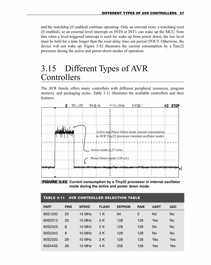
and the watchdog (if enabled) continue operating. Only an external reset, a watchdog reset(if enabled), or an external level interrupt on INT0 or INT1 can wake up the MCU. Notethat when a level-triggered interrupt is used for wake up from power down, the low levelmust be held for a time longer than the reset delay time-out period tTOUT. Otherwise, thedevice will not wake up. Figure 3.42 illustrates the current consumption by a Tiny22processor during the active and power-down modes of operation.
3.15 Different Types of AVRControllersThe AVR family offers many controllers with different peripheral resources, programmemory, and packaging styles. Table 3.11 illustrates the available controllers and their features.
DIFFERENT TYPES OF AVR CONTROLLERS 57
Active and Power Down mode current consumptionin AVR Tiny22 processor (internal oscillator mode)
Active mode (3.57 mA)
Power Down mode (120 uA)
FIGURE 3.42 Current consumption by a Tiny22 processor in internal oscillatormode during the active and power down mode.
TABLE 3-11 AVR CONTROLLER SELECTION TABLE
PART PINS SPEED FLASH EEPROM RAM UART ADC
90S1200 20 16 MHz 1 K 64 0 No No
90S2313 20 10 MHz 2 K 128 128 Yes No
90S2323 8 10 MHz 2 K 128 128 No No
90S2343 8 10 MHz 2 K 128 128 No No
90S2333 28 10 MHz 2 K 128 128 Yes Yes
90S4433 28 10 MHz 4 K 256 128 Yes Yes
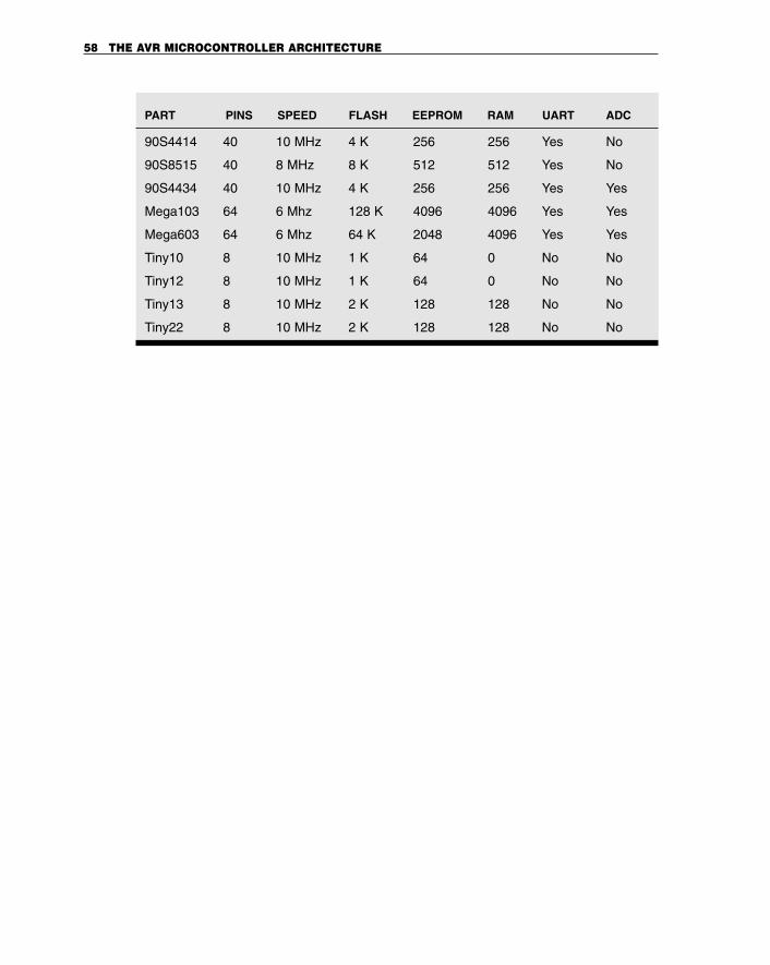
58 THE AVR MICROCONTROLLER ARCHITECTURE
PART PINS SPEED FLASH EEPROM RAM UART ADC
90S4414 40 10 MHz 4 K 256 256 Yes No
90S8515 40 8 MHz 8 K 512 512 Yes No
90S4434 40 10 MHz 4 K 256 256 Yes Yes
Mega103 64 6 Mhz 128 K 4096 4096 Yes Yes
Mega603 64 6 Mhz 64 K 2048 4096 Yes Yes
Tiny10 8 10 MHz 1 K 64 0 No No
Tiny12 8 10 MHz 1 K 64 0 No No
Tiny13 8 10 MHz 2 K 128 128 No No
Tiny22 8 10 MHz 2 K 128 128 No No
The Instruction set of a processor or a controller is like the vocabulary of the processor.Each instruction controls some part of the processor and allows the programmer to manip-ulate data in the memory as well as input and output devices.
The instructions of the processor can be categorized in many different ways based onhow the instructions access data and operate upon it. This is called the program and dataaddressing modes of the processor.
4.1 Program and Data AddressingModesThe various AVR instructions can be categorized in about 10 different addressing modes.Each instruction has an opcode that indicates to the control logic of the processor what todo. The other part of the instruction is the operand, on which the opcode operates.
4.1.1 REGISTER DIRECT (SINGLE REGISTER)
The Register Direct instructions can operate on any of the 32 registers of the register file.It reads the contents of a register, operates on the contents of the register, and then stores
4THE AVR INSTRUCTION SET
59
Copyright 2001 The McGraw-Hill Companies, Inc. Click Here for Terms of Use.
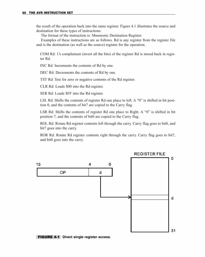
the result of the operation back into the same register. Figure 4.1 illustrates the source anddestination for these types of instructions.
The format of the instruction is: Mnemonic Destination Register.Examples of these instructions are as follows. Rd is any register from the register file
and is the destination (as well as the source) register for the operation.
COM Rd: 1’s complement (invert all the bits) of the register Rd is stored back in regis-ter Rd.
INC Rd: Increments the contents of Rd by one.
DEC Rd: Decrements the contents of Rd by one.
TST Rd: Test for zero or negative contents of the Rd register.
CLR Rd: Loads $00 into the Rd register.
SER Rd: Loads $FF into the Rd register.
LSL Rd: Shifts the contents of register Rd one place to left. A “0” is shifted in bit posi-tion 0, and the contents of bit7 are copied to the Carry flag.
LSR Rd: Shifts the contents of register Rd one place to Right. A “0” is shifted in bitposition 7, and the contents of bit0 are copied to the Carry flag.
ROL Rd: Rotate Rd register contents left through the carry. Carry flag goes to bit0, andbit7 goes into the carry.
ROR Rd: Rotate Rd register contents right through the carry. Carry flag goes to bit7,and bit0 goes into the carry.
60 THE AVR INSTRUCTION SET
FIGURE 4-1 Direct single register access.
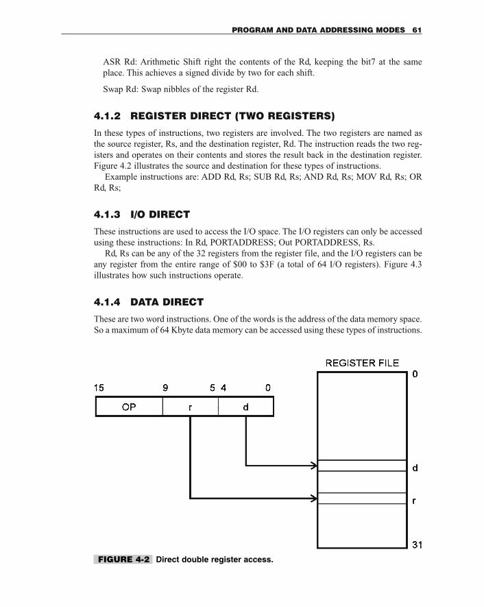
ASR Rd: Arithmetic Shift right the contents of the Rd, keeping the bit7 at the sameplace. This achieves a signed divide by two for each shift.
Swap Rd: Swap nibbles of the register Rd.
4.1.2 REGISTER DIRECT (TWO REGISTERS)
In these types of instructions, two registers are involved. The two registers are named asthe source register, Rs, and the destination register, Rd. The instruction reads the two reg-isters and operates on their contents and stores the result back in the destination register.Figure 4.2 illustrates the source and destination for these types of instructions.
Example instructions are: ADD Rd, Rs; SUB Rd, Rs; AND Rd, Rs; MOV Rd, Rs; ORRd, Rs;
4.1.3 I/O DIRECT
These instructions are used to access the I/O space. The I/O registers can only be accessedusing these instructions: In Rd, PORTADDRESS; Out PORTADDRESS, Rs.
Rd, Rs can be any of the 32 registers from the register file, and the I/O registers can beany register from the entire range of $00 to $3F (a total of 64 I/O registers). Figure 4.3illustrates how such instructions operate.
4.1.4 DATA DIRECT
These are two word instructions. One of the words is the address of the data memory space.So a maximum of 64 Kbyte data memory can be accessed using these types of instructions.
PROGRAM AND DATA ADDRESSING MODES 61
FIGURE 4-2 Direct double register access.
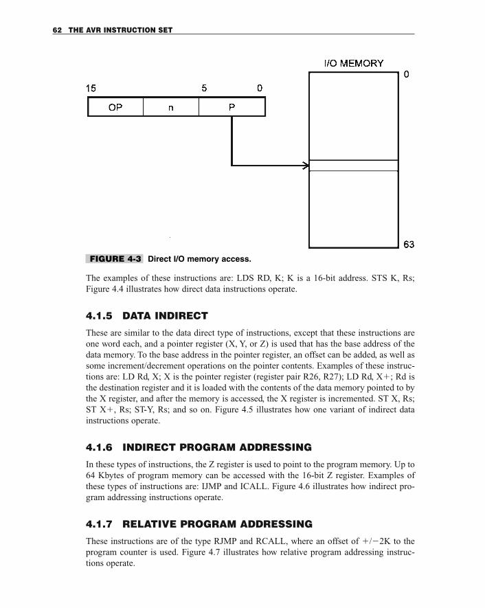
The examples of these instructions are: LDS RD, K; K is a 16-bit address. STS K, Rs;Figure 4.4 illustrates how direct data instructions operate.
4.1.5 DATA INDIRECT
These are similar to the data direct type of instructions, except that these instructions areone word each, and a pointer register (X, Y, or Z) is used that has the base address of thedata memory. To the base address in the pointer register, an offset can be added, as well assome increment/decrement operations on the pointer contents. Examples of these instruc-tions are: LD Rd, X; X is the pointer register (register pair R26, R27); LD Rd, X�; Rd isthe destination register and it is loaded with the contents of the data memory pointed to bythe X register, and after the memory is accessed, the X register is incremented. ST X, Rs;ST X�, Rs; ST-Y, Rs; and so on. Figure 4.5 illustrates how one variant of indirect datainstructions operate.
4.1.6 INDIRECT PROGRAM ADDRESSING
In these types of instructions, the Z register is used to point to the program memory. Up to64 Kbytes of program memory can be accessed with the 16-bit Z register. Examples ofthese types of instructions are: IJMP and ICALL. Figure 4.6 illustrates how indirect pro-gram addressing instructions operate.
4.1.7 RELATIVE PROGRAM ADDRESSING
These instructions are of the type RJMP and RCALL, where an offset of �/�2K to theprogram counter is used. Figure 4.7 illustrates how relative program addressing instruc-tions operate.
62 THE AVR INSTRUCTION SET
FIGURE 4-3 Direct I/O memory access.
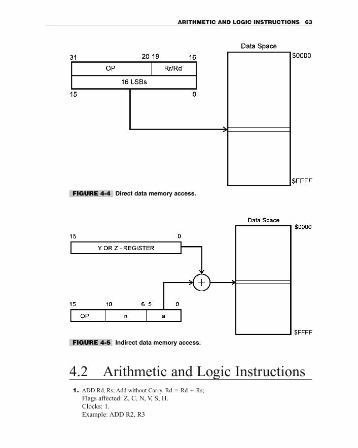
4.2 Arithmetic and Logic Instructions1. ADD Rd, Rs; Add without Carry. Rd � Rd � Rs;
Flags affected: Z, C, N, V, S, H.Clocks: 1.Example: ADD R2, R3
ARITHMETIC AND LOGIC INSTRUCTIONS 63
FIGURE 4-4 Direct data memory access.
FIGURE 4-5 Indirect data memory access.
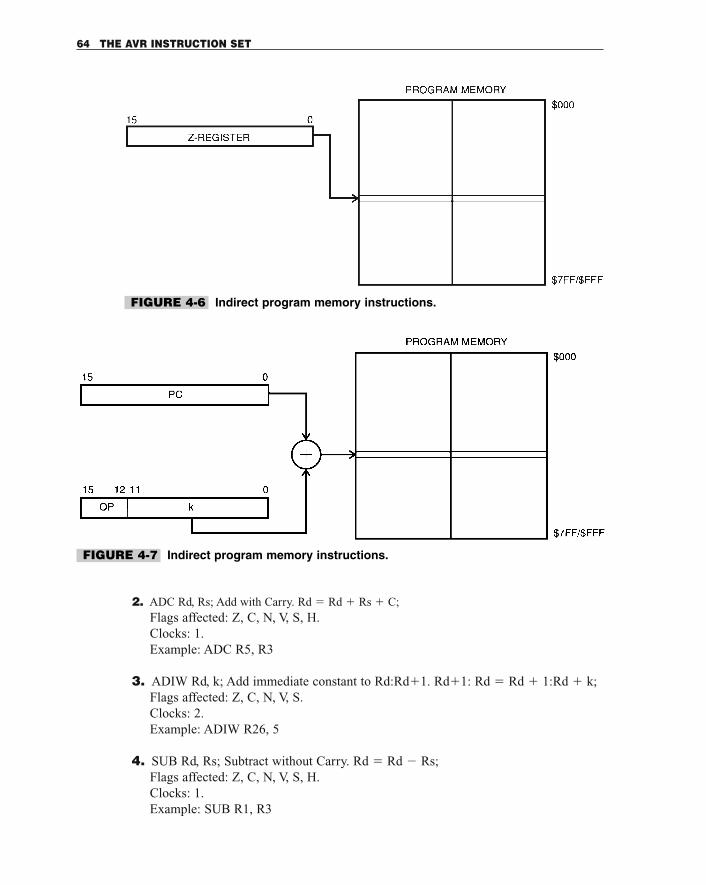
2. ADC Rd, Rs; Add with Carry. Rd � Rd � Rs � C;Flags affected: Z, C, N, V, S, H.Clocks: 1.Example: ADC R5, R3
3. ADIW Rd, k; Add immediate constant to Rd:Rd�1. Rd�1: Rd � Rd � 1:Rd � k;Flags affected: Z, C, N, V, S.Clocks: 2.Example: ADIW R26, 5
4. SUB Rd, Rs; Subtract without Carry. Rd � Rd � Rs;Flags affected: Z, C, N, V, S, H.Clocks: 1.Example: SUB R1, R3
64 THE AVR INSTRUCTION SET
FIGURE 4-6 Indirect program memory instructions.
FIGURE 4-7 Indirect program memory instructions.
5. SUBI Rd, k; Subtract immediate without Carry. Rd � Rd � k;Flags affected: Z, C, N, V, S, H. Clocks:1.Example: SUBI R5, 10
6. SBCI Rd, k; Subtract immediate with Carry. Rd � Rd � k �C;Flags affected: Z, C, N, V, S, H.Clocks: 1.Example: SBCI R10, 2
7. SBC Rd, Rs; Subtract with Carry. Rd � Rd � Rs � C;Flags affected: Z, C, N, V, S, H.Clocks: 1.Example: SBC R5, R3
8. SBIW Rd, k; Subtract immediate constant from Rd:Rd � 1. Rd � 1: Rd � Rd � 1:Rd � k;Flags affected: Z, C, N, V, S.Clocks: 2.Example: SBIW R26, 5
9. AND Rd, Rs; Logical AND Rd and Rs. Rd � Rd & Rs.Flags affected: Z, N, V, S.Clocks: 1.Example: AND R26, R2
10. ANDI Rdx, k; Logical AND Rdx and k. Rdx � Rd & k. Rdx is between R16 andR31l; k is an 8-bit constant.Flags affected: Z, N, V, S.Clocks: 1.Example: ANDI R26, 5
11. OR Rd, Rs; Logical OR Rd with Rs. Rd � Rd | Rs.Flags affected: Z, N, V, S.Clocks: 1.Example: OR R1, R2
12. ORI Rdx, k; Logical OR Rdx with k. Rdx � Rd | k. Rdx is between R16 and R31; kis an 8-bit constant.Flags affected: Z, N, V, S.Clocks: 1.Example: ORI R16, 0b11110000
13. EOR Rd, Rs; Exclusive OR Rd with Rs. Rd � Rd Exor Rs.Flags affected: Z, N, V, S.Clocks: 1.Example: EOR R1, R2
ARITHMETIC AND LOGIC INSTRUCTIONS 65
14. COM Rd; One’s complement Rd. Rd � $FF � Rd.Flags affected: Z, C, N, V, S.Clocks: 1.Example: COM R1
15. NEG Rd; Two’s complement Rd. Rd � $00 � Rd.Flags affected: Z, C, N, V, S, H.Clocks: 1.Example: NEG R30
16. SBR Rdx, k; Set bit(s) in Rdx. Rdx � Rdx v k. Rdx is between R16 and R31.Flags affected: Z, N, V, S.Clocks: 1.Example: SBR R30, 5
17. CBR Rdx, k; Clear bit(s) in Rdx. Rdx � Rdx & ($FF�k). Rdx is between R16 andR31.Flags affected: Z, N, V, S.Clocks: 1.Example: CBR R28, 5
18. INC Rd; Increment contents of Rd. Rd � Rd � 1.Flags affected: Z, N, V, S.Clocks: 1.Example: INC R3
19. DEC Rd; Decrement contents of Rd. Rd � Rd � 1.Flags affected: Z, N, V, S.Clocks: 1.Example: DEC R2
20. TST Rd; Test Rd for zero or minus. Rd � Rd & Rd.Flags affected: Z, N, V, S.Clocks: 1.Example: TST R2
21. MUL Rd, Rs; Unsigned multiplication of Rd and Rs. The result is stored in R1:R0.R1: R0 � Rd � Rs.Flags affected: Z, C.Clocks: 2.Example: MUL R3, R2
22. MULS Rd, Rs; Signed multiplication of Rd and Rs. The result is stored in R1: R0.R1: R0 � Rd � Rs.Flags affected: Z, C.Clocks: 2.Example: MULS R4, R5
66 THE AVR INSTRUCTION SET
23. MULSU Rd, Rs; Signed multiplication of Rd (signed) and Rs (unsigned). The resultis stored in R1: R0. R1: R0 � Rd � Rs.Flags affected: Z, C.Clocks: 2.Example: MULSU R4, R5
24. FMUL Rd, Rs; Unsigned fractional multiplication of Rd(1.7 format) and Rs(1.7 for-mat). The result is stored in R1: R0(1.15 format). R1: R0 � Rd � Rs.Flags affected: Z, C.Clocks: 2.Example: FMUL R30, R31
25. FMULS Rd, Rs; Signed fractional multiplication of Rd (1.7 format) and Rs (1.7 for-mat). The result is stored in R1:R0 (1.15 format). R1: R0 � Rd � Rs.Flags affected: Z, C.Clocks: 2.Example: FMULS R4, R5
26. FMULSU Rd, Rs; Fractional Signed multiplication of Rd (signed, 1.7 format) and Rs(unsigned, 1.7 format). The result is stored in R1: R0 (signed 1.15 format). R1: R0 �Rd � Rs.Flags affected: Z, C.Clocks: 2.Example: FMULSU R4, R5
27. CLR Rd; Clear Register Rd
28. SER Rd; Set Register Rd
4.3 Program Control Instructions
1. RJMP k; Relative jump to a location in program memory. K is �/� 2K addresses.Flags affected: none.Clocks: 2.Example:RJMP OKNOT_OK: ADD R1, R5OK: INC R1
2. IJMP; Indirect jump to a location in program memory pointed by the Z register.Flags affected: none.Clocks: 2.Example:ldi r30, add_lowldi r31, add_highIJMP
PROGRAM CONTROL INSTRUCTIONS 67
3. JMP k; Jump to a location in program memory.Flags affected: none.Clocks: 3.Example:JMP go_far;;;go_far:
4. 4. RCALL k; relative call to a subroutine.Flags affected: none.Clocks: 3/4.Example: rcall my_subroutine
5. ICALL; Indirect call to a subroutine.Flags affected: none.Clocks: 3/4.Example:ldi r30, farsub_lowldi r31, farsub_highicall
6. CALL k; call to a subroutine.Flags affected: none.Clocks: 4/5.Example: call my_subroutine
7. RET; Subroutine return.Flags affected: none.Clocks: 4/5.Example:;;POP SREGRET
8. RETI; Interrupt return.Flags affected: I.Clocks: 4/5.Example:;;POP SREGRETI
68 THE AVR INSTRUCTION SET
9. CPSE Rd, Rs; Compare, Skip if Equal. If Rd � Rs, skip next instruction.Flags affected: none.Clocks: 1/2/3Example:back_here: CPSE r3, r4rjmp back_herein r3, PINB
10. CP Rd, Rs; Compare. Rd � Rs.Flags affected: Z, C, N, V, S, H.Clocks: 1Example:CP r18, r19breq some_place
11. CPC Rd, Rs; Compare with carry. Rd � Rs � C.Flags affected: Z, C, N, V, S, H.Clocks: 1Example:CP r18, r20CPC r19, r21brne some_place
12. CPI Rdx, k; Compare with carry. Rdx � k. Rd is between r16 and r31.Flags affected: Z, C, N, V, S, H.Clocks: 1Example:CPI r18, 0breq some_place
13. SBRC Rd, b; Skip if bit in register cleared. If [Rd(b) � 0], skip next instruction.Flags affected: none.Clocks: 1/2/3Example:back_here: in r3, PINBSBRC r3, 0rjmp back_herein r4, PIND
14. SBRS Rd, b; Skip if bit in register set. If [Rd(b) � 1], skip next instruction.lags affected: none.Clocks: 1/2/3Example:back_here: in r3, PINBSBRS r3, 0
PROGRAM CONTROL INSTRUCTIONS 69
rjmp back_herein r4, PIND
15. SBIC A, b; Skip if bit in I/O register cleared. If [A(b) � 0], skip next instruction.Flags affected: none.Clocks: 1/2/3Example:back_here: SBIC PINB, 0rjmp back_herein r4, PIND
16. SBIC A, b; Skip if bit in I/O register set. If [A(b) � 1], skip next instruction.Flags affected: none.Clocks: 1/2/3Example:back_here: SBIS PINB, 0rjmp back_herein r4, PIND
17. BRBS s, k; Branch if status flag set. conditional relative branch. If flag s in the SREG is set, then branch k relative to the PC.Flags affected: none.Clocks: 1/2
18. BRBC s, k; Branch if status flag cleared. conditional relative branch. If flag s in the SREG is cleared, then branch k relative to the PC.Flags affected: none.Clocks: 1/2
19. BREQ k; Branch if Equal. If Z � 1, then branch relative.Flags affected: none.Clocks: 1/2
20. BRNE k; Branch if Not Equal. If Z � 0, then branch relative.Flags affected: none.Clocks: 1/2
21. BRCS k; Branch if Carry set. If C � 1, then branch relative.Flags affected: none.Clocks: 1/2
22. BRCC k; Branch if Carry cleared. If C � 0, then branch relative.Flags affected: none.Clocks: 1/2
70 THE AVR INSTRUCTION SET
23. BRSH k; Branch if same or higher. If C � 0, then branch relative.Flags affected: none.Clocks: 1/2
24. BRLO k; Branch if lower. If C � 1, then branch relative.Flags affected: none.Clocks: 1/2
25. BRMI k; Branch if minus. If N � 1, then branch relative.Flags affected: none.Clocks: 1/2
26. BRPL k; Branch if plus. If N � 0, then branch relative.Flags affected: none.Clocks: 1/2
27. BRGE k; Branch if greater or equal, signed. If (N Exor V) � 0, then branch relative.Flags affected: none.Clocks: 1/2
28. BRLT k; Branch if less than, signed. If (N Exor V) � 1, then branch relative.Flags affected: none.Clocks: 1/2
29. BRHS k; Branch if Half carry flag set. If H � 1, then branch relative.Flags affected: none.Clocks: 1/2
30. BRHC k; Branch if Half carry flag cleared. If H � 0, then branch relative.Flags affected: none.Clocks: 1/2
31. BRTS k; Branch if T flag set. If T � 1, then branch relative.Flags affected: none.Clocks: 1/2
32. BRTC k; Branch if T flag cleared. If T � 0, then branch relative.Flags affected: none.Clocks: 1/2
33. BRVS k; Branch if Overflow flag set. If V � 1, then branch relative.Flags affected: none.Clocks: 1/2
34. BRVC k; Branch if Overflow flag cleared. If V � 0, then branch relative.Flags affected: none.Clocks: 1/2
PROGRAM CONTROL INSTRUCTIONS 71
35. BRIE k; Branch if Interrupts enabled. If I � 1, then branch relative.Flags affected: none.Clocks: 1/2
36. BRID k; Branch if Interrupt disabled. If I � 0, then branch relative.Flags affected: none.Clocks: 1/2
4.4 Data Transfer Instructions
1. MOV Rd, Rs; Copy register. Rd � Rs.Flags affected: None.Clocks: 1.Example: MOV R2, R18
2. MOVW Rd, Rs; Copy register pair. Rd�1: Rd � Rs � 1: Rs.Flags affected: None.Clocks: 1.Example: MOV R26, R30
3. LDI Rdx, k; Load Immediate. Rdx � k. Rdx is between r16 and r31.Flags affected: None.Clocks: 1.Example: LDI R18, $53
4. LDS Rd, k; Load Immediate. Rd � data memory(k).Flags affected: None.Clocks: 2.Example: LDS R1, $5300
5. LD Rd, X; Load Indirect. Rd � data memory(X). X is the pointer register pair R26:R27.Flags affected: None.Clocks: 2.Example: LD R1, X
6. LD Rd, X�; Load Indirect. Rd � data memory(X), X � X �1. X is the pointerregister pair R26: R27.Flags affected: None.Clocks: 2.Example: LD R15, X�
72 THE AVR INSTRUCTION SET
7. LD Rd, �X; Load Indirect. X � X �1, Rd � data memory(X). X is the pointer reg-ister pair R26: R27.Flags affected: None.Clocks: 2.Example: LD R15, �X
8. LD Rd, Y; Load Indirect. Rd � data memory (Y). Y is the pointer register pair R28:R29.Flags affected: None.Clocks: 2.Example: LD R1, Y
9. LD Rd, Y�; Load Indirect. Rd � data memory (Y), Y � Y � 1. Y is the pointer reg-ister pair R28: R29.Flags affected: None.Clocks: 2.Example: LD R15, Y�
10. LD Rd, �Y; Load Indirect. Y � Y � 1, Rd � data memory(Y). Y is the pointer reg-ister pair R28: R29.Flags affected: None.Clocks: 2.Example: LD R15, �Y
11. LDD Rd, Y�q; Load Indirect with displacement. Rd � data memory(Y � q). Y is thepointer register pair R28: R29.Flags affected: None.Clocks: 2.Example: LD R15, Y�2
12. LD Rd, Z; Load Indirect. Rd � data memory(Z). Z is the pointer register pair R30:R31.Flags affected: None.Clocks: 2.Example: LD R1, Z
13. LD Rd, Z�; Load Indirect. Rd � data memory(Z), Z � Z � 1; Z is the pointer reg-ister pair R30: R31.Flags affected: None.Clocks: 2.Example: LD R15, Z�
14. LD Rd, �Z; Load Indirect. Z � Z � 1, Rd � data memory(Z). Z is the pointer reg-ister pair R30: R31.Flags affected: None.
DATA TRANSFER INSTRUCTIONS 73
Clocks: 2.Example: LD R15, �Z
15. LDD Rd, Z�q; Load Indirect with displacement. Rd � data memory(Z � q). Z is thepointer register pair R30: R31.Flags affected: None.Clocks: 2.Example: LD R15, Z�5
16. STS Rs, k; Store Immediate. data memory(k) � Rs.Flags affected: None.Clocks: 2.Example: STS $5300, R1
17. ST X, Rs; Store Indirect. data memory(X) � Rs. X is the pointer register pair R26:R27.Flags affected: None.Clocks: 2.Example: ST X, R1
18. ST X�, Rs; Store Indirect. data memory(X) � Rs, X � X �1. X is the pointer reg-ister pair R26: R27.Flags affected: None.Clocks: 2.Example: ST X�, R15
19. ST �X, Rs; Store Indirect. X � X �1, data memory(X) � Rs. X is the pointer reg-ister pair R26: R27.Flags affected: None.Clocks: 2.Example: ST �X, R11
20. ST Y, RD; Store Indirect. data memory(Y) � Rs. Y is the pointer register pair R28:R29.Flags affected: None.Clocks: 2.Example: ST Y, R1
21. ST Y�, Rs; Store Indirect. data memory(Y) � Rs, Y � Y �1; Y is the pointer regis-ter pair R28: R29.Flags affected: None.Clocks: 2.Example: ST Y�, R5
22. ST �Y, Rs; Store Indirect. Y � Y � 1, data memory(Y) � Rs. Y is the pointer reg-ister pair R28: R29.Flags affected: None.
74 THE AVR INSTRUCTION SET
Clocks: 2.Example: ST �Y, R5
23. STD Y � q, Rs; Store Indirect with displacement. data memory(Y � q) � Rs. Y isthe pointer register pair R28: R29.Flags affected: None.Clocks: 2.Example: STD Y�2, R8
24. ST Z, RD; Store Indirect. data memory(Z) � Rs. Z is the pointer register pair R30:R31.Flags affected: None.Clocks: 2.Example: ST Z, R1
25. ST Z�, Rs; Store Indirect. data memory(Z) � Rs, Z � Z �1; Z is the pointer regis-ter pair R30: R31.Flags affected: None.Clocks: 2.Example: ST Z�, R5
26. ST �Z, Rs; Store Indirect. Z � Z � 1, data memory(Z) � Rs. Z is the pointer regis-ter pair R30: R31.Flags affected: None.Clocks: 2.Example: ST �Z, R5
27. STD Z�q, Rs; Store Indirect with displacement. data memory(Z�q) � Rs. Z is thepointer register pair R30: R31.Flags affected: None.Clocks: 2.Example: STD Z�2, R8
28. LPM; Load Program Memory. R0 � Program Memory(Z). Z is the pointer registerpair R30: R31.Flags affected: None.Clocks: 3.
29. LPM Rd, Z; Load Program Memory. Rd 5 Program Memory(Z). Z is the pointer reg-ister pair R30: R31.Flags affected: None.Clocks: 3.Example: LPM R2, Z
30. LPM Rd, Z�; Load Program Memory. Rd � Program Memory(Z), Z � Z � 1. Z isthe pointer register pair R30: R31.Flags affected: None.
DATA TRANSFER INSTRUCTIONS 75
Clocks: 3.Example: LPM R20, Z�
31. IN Rd, A; Input from Input Port. Rd � I/OPort(A),Flags affected: None.Clocks: 1.Example: IN r1, PINB
32. OUT A, Rs; Output to output Port. I/OPort(A) � Rs,Flags affected: None.Clocks: 1.Example: OUT PORTB, R16
33. PUSH Rs; Push register on STACK. STACK � Rs,Flags affected: None.Clocks: 2.Example: PUSH r1
34. POP Rd; Pop into register from STACK. Rd � STACK,Flags affected: None.Clocks: 2.Example: POP r1
4.5 Bit and Bit-test Instructions
1. LSL Rd; Logical Shift Left. Rd(n�1) � Rd(n); Rd(0) � 0; C � Rd(7).Flags affected: Z, C, N, V, H.Clocks: 1.Example: LSL r1
2. LSR Rd; Logical Shift Right. Rd(n) � Rd(n�1); Rd(7) � 0; C � Rd(0).Flags affected: Z, C, N, V.Clocks: 1.Example: LSR r10
3. ROL Rd; Rotate Left though Carry. Rd(0) � C; Rd(n�1) � Rd(n); C � Rd(7).Flags affected: Z, C, N, V, H.Clocks: 1.Example: ROL r13
4. ROR Rd; Rotate Right through Carry. Rd(7) � C; Rd(n) � Rd(n�1); C � Rd(0).Flags affected: Z, C, N, V.Clocks: 1.Example: ROR r10
76 THE AVR INSTRUCTION SET
5. ASR Rd; Arithmetic Shift Right. Rd(n) � Rd(n�1), for n � 0 to 6;Flags affected: Z, C, N, V.Clocks: 1.Example: ASR r10
6. SWAP Rd; Swap Nibbles. exchange Rd(3,2,1,0) with Rd(7,6,5,4)Flags affected: None.Clocks: 1.Example: SWAP r10
7. BSET s; Flag Set. SREG(s) � 1;Flags affected: SREG(s).Clocks: 1.Example: BSET 7
8. BCLR s; Flag Reset. SREG(s) � 0;Flags affected: SREG(s).Clocks: 1.Example: BCLR 7
9. SBI A, s; Set bit s in I/O register A. I/O(A,s) � 1;Flags affected: none.Clocks: 1.Example: SBI PORTD, 7
10. CBI A, s; Clear bit s in I/O register A. I/O(A,s) � 0;Flags affected: none.Clocks: 1.Example: CBI PORTD, 7
11. BST Rs, s; Bit Store from Rs to T flag. T � Rs(s);Flags affected: T.Clocks: 1.Example: BST R1, 2
12. BLD Rd, s; Bit Store from T flag to Rd. Rd(s) � T;Flags affected: none.Clocks: 1.Example: BLD R4, 2
13. SEC; Set Carry flag. C � 1;Flags affected: C.Clocks: 1.Example: SEC
14. CLC; Clear Carry flag. C � 0;Flags affected: C.
BIT AND BIT-TEST INSTRUCTIONS 77
Clocks: 1.Example: CLC
15. SEN; Set Negative flag. N � 1;Flags affected: N.Clocks: 1.Example: SEN
16. CLN; Clear Negative flag. N � 0;Flags affected: N.Clocks: 1.Example: CLN
17. SEZ; Set Zero flag. Z � 1;Flags affected: Z.Clocks: 1.Example: SEZ
18. CLZ; Clear Zero flag. Z � 0;Flags affected: Z.Clocks: 1.Example: CLZ
19. SEI; Set Interrupt flag. I � 1;Flags affected: I.Clocks: 1.Example: SEI
20. CLI; Clear Interrupt flag. I � 0;Flags affected: I.Clocks: 1.Example: CLI
21. SES; Set Signed Test flag. S � 1;Flags affected: S.Clocks: 1.Example: SES
22. CLS; Clear Signed Test flag. S � 0;Flags affected: S.Clocks: 1.Example: CLS
23. SEV; Set Two’s Complement flag. V � 1;Flags affected: V.Clocks: 1.Example: SEV
78 THE AVR INSTRUCTION SET
24. CLV; Clear Two’s Complement flag. V � 0;Flags affected: V.Clocks: 1.Example: CLV
25. SET; Set T flag. T � 1;Flags affected: T.Clocks: 1.Example: SET
26. CLT; Clear T flag. T � 0;Flags affected: T.Clocks: 1.Example: CLT
27. SEH; Set Half Carry flag. H � 1;Flags affected: H.Clocks: 1.Example: SEH
28. CLH; Clear Half Carry flag. H � 0;Flags affected: H.Clocks: 1.Example: CLH
29. NOP; No Operation;Flags affected: none.Clocks: 1.Example: NOP
30. SLEEP; Sleep;Flags affected: none.Clocks: 1.Example: SLEEP
31. WDR; Watchdog Reset;Flags affected: none.Clocks: 1.Example: WDR
BIT AND BIT-TEST INSTRUCTIONS 79

This page intentionally left blank.
What does it take to get a simple AVR-based circuit up and running? Well, it would takea processor, voltage source, clock generation circuit, and a suitable reset circuit for reliableoperation.
Figure 5.1 illustrates this simple configuration. The external clock generation circuit isoptional, as many of the AVR processors have an internal RC oscillator that is used whenfeasible. Let us look at these issues in some detail.
5.1 Power SourceThe power source for running a processor system is a critical component. No system wouldrun without a power supply. There are various options that the designer may consider,depending upon the application. Broadly, the choice would be dictated by whether the sys-tem is portable and hence must use a battery source or whether it is for a desktop applica-tion, where an AC power line could be used.
Sometimes you may have access to an AC power line, but the battery operation mayseem more convenient simply because it offers added portability and does not require abulky transformer and associated rectifier, filter, and regulator components.
5AVR HARDWARE DESIGN ISSUES
81
Copyright 2001 The McGraw-Hill Companies, Inc. Click Here for Terms of Use.
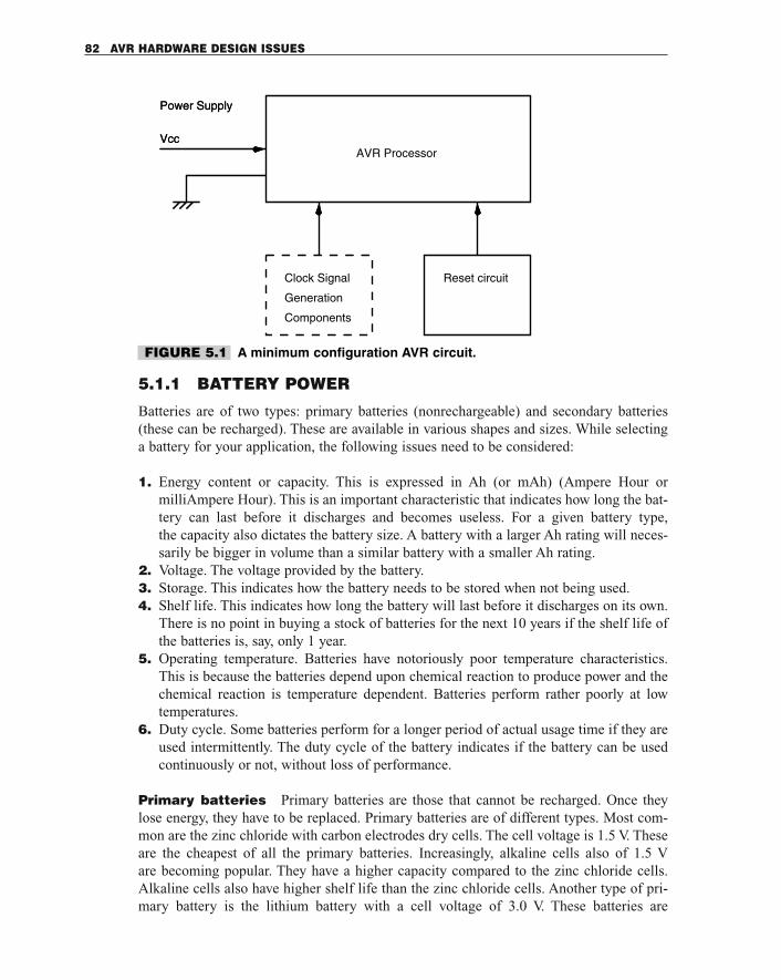
5.1.1 BATTERY POWER
Batteries are of two types: primary batteries (nonrechargeable) and secondary batteries(these can be recharged). These are available in various shapes and sizes. While selectinga battery for your application, the following issues need to be considered:
1. Energy content or capacity. This is expressed in Ah (or mAh) (Ampere Hour ormilliAmpere Hour). This is an important characteristic that indicates how long the bat-tery can last before it discharges and becomes useless. For a given battery type, the capacity also dictates the battery size. A battery with a larger Ah rating will neces-sarily be bigger in volume than a similar battery with a smaller Ah rating.
2. Voltage. The voltage provided by the battery.3. Storage. This indicates how the battery needs to be stored when not being used.4. Shelf life. This indicates how long the battery will last before it discharges on its own.
There is no point in buying a stock of batteries for the next 10 years if the shelf life ofthe batteries is, say, only 1 year.
5. Operating temperature. Batteries have notoriously poor temperature characteristics.This is because the batteries depend upon chemical reaction to produce power and thechemical reaction is temperature dependent. Batteries perform rather poorly at lowtemperatures.
6. Duty cycle. Some batteries perform for a longer period of actual usage time if they areused intermittently. The duty cycle of the battery indicates if the battery can be usedcontinuously or not, without loss of performance.
Primary batteries Primary batteries are those that cannot be recharged. Once theylose energy, they have to be replaced. Primary batteries are of different types. Most com-mon are the zinc chloride with carbon electrodes dry cells. The cell voltage is 1.5 V. Theseare the cheapest of all the primary batteries. Increasingly, alkaline cells also of 1.5 V are becoming popular. They have a higher capacity compared to the zinc chloride cells.Alkaline cells also have higher shelf life than the zinc chloride cells. Another type of pri-mary battery is the lithium battery with a cell voltage of 3.0 V. These batteries are
82 AVR HARDWARE DESIGN ISSUES
Vcc
Power Supply
Vcc
Generation
Components
Reset circuit
AVR Processor
Clock Signal
Power Supply
FIGURE 5.1 A minimum configuration AVR circuit.
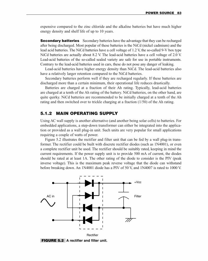
expensive compared to the zinc chloride and the alkaline batteries but have much higherenergy density and shelf life of up to 10 years.
Secondary batteries Secondary batteries have the advantage that they can be rechargedafter being discharged. Most popular of these batteries is the NiCd (nickel cadmium) and thelead acid batteries. The NiCd batteries have a cell voltage of 1.2 V, the so-called 9-V box typeNiCd batteries are actually about 8.2 V. The lead-acid batteries have a cell voltage of 2.0 V.Lead-acid batteries of the so-called sealed variety are safe for use in portable instruments.Contrary to the lead-acid batteries used in cars, these do not pose any danger of leaking.
Lead-acid batteries have higher energy density than NiCd. The lead-acid batteries alsohave a relatively larger retention compared to the NiCd batteries.
Secondary batteries perform well if they are recharged regularly. If these batteries aredischarged more than a certain minimum, their operational life reduces drastically.
Batteries are charged at a fraction of their Ah rating. Typically, lead-acid batteries are charged at a tenth of the Ah rating of the battery. NiCd batteries, on the other hand, arequite quirky. NiCd batteries are recommended to be initially charged at a tenth of the Ahrating and then switched over to trickle charging at a fraction (1/50) of the Ah rating.
5.1.2 MAIN OPERATING SUPPLY
Using AC wall supply is another alternative (and another being solar cells) to batteries. Forembedded applications, a step-down transformer can either be integrated into the applica-tion or provided as a wall plug-in unit. Such units are very popular for small applicationsrequiring a couple of watts of power.
Figure 5.2 illustrates the rectifier and filter unit that can be fed by a wall plug-in trans-former. The rectifier could be built with discrete rectifier diodes (such as 1N4001), or evena complete rectifier unit be used. The rectifier should be suitably rated, keeping in mind thecurrent requirements. If the power supply unit is to provide 500 mA of current, the diodesshould be rated at at least 1A. The other rating of the diode to consider is the PIV (peakinverse voltage). This is the maximum peak reverse voltage that the diode can withstandbefore breaking down. An 1N4001 diode has a PIV of 50 V, and 1N4007 is rated to 1000 V.
POWER SOURCE 83
+Vcc
Rectifier
FilterAC in
FIGURE 5.2 A rectifier and filter unit.
The peak rectified voltage that appears at the filter capacitor is 1.4 times the AC inputvoltage (AC input voltage is a RMS figure). A 10-V AC input will generate about 14 V DCvoltage on the filter capacitor. The filter capacitor must be of sufficiently large capacity toprovide sustained current. The filter capacitor must also be rated to handle the DC voltage.For a 14-V DC, at least a 25 V rating capacitor should be employed.
5.1.3 POWER FROM PORT SIGNAL LINES
Another source of power that is available most often if you are using a PC together withyour application is the PC port signal lines, such as the parallel port and the serial RC232port. If the PC is equipped with a USB port, it can be used to provide �5 V that is avail-able on a USB connector.
I have used the RS-232 signal power in many low-power applications. The RS-232 sig-nals can provide up to 10 mA each. The output signals of the RS-232 port that can be usedto provide supply voltage are:
1. TxD: Output data signal from the RS-232 port. When idling, this signal is at �12 Vand can be used to provide -ve voltage to the circuit.
2. DTR: Data Terminal Ready. Output signal used for communicating with a modem. Thiscan be used to provide either �12 or �12 V supply. However, when the signal isloaded, the voltage drops. Usually, a micropower regulator or even a zener diode can beused to get a lower supply voltage for the AVR processor.
3. RTS: Request to Send. Output control signal used for communicating with an externaldevice. Can be used in a fashion similar to the DTR signal.
The DTR and the RTS signals are controlled by the Modem Control Register (MCR) ina PC. The MCR is at an address offset 4 from the RS-232 base address. By writing $01 tothe MCR, the DTR is set to �12 V and by writing $02, the RTS is set to �12 V, while writ-ing $03 to the MCR, both the RTS and the DTR are set to �12. Table 5.1 illustrates all thecombinations of voltages that you can get on the DTR and the RTS signal pins by writingthe appropriate control word to the MCR.
The following C code (rspower.c) shows how to put both the DTR and the RTS signalto �12 V.
84 AVR HARDWARE DESIGN ISSUES
TABLE 5-1 MCR CONTROL VALUES FOR DTR AND RTS SIGNAL VOLTAGES
MCR VALUE RTS VOLTAGE DTR VOLTAGE
0 �12 V �12 V
1 �12 V �12 V
2 �12 V �12 V
3 �12 V �12 V
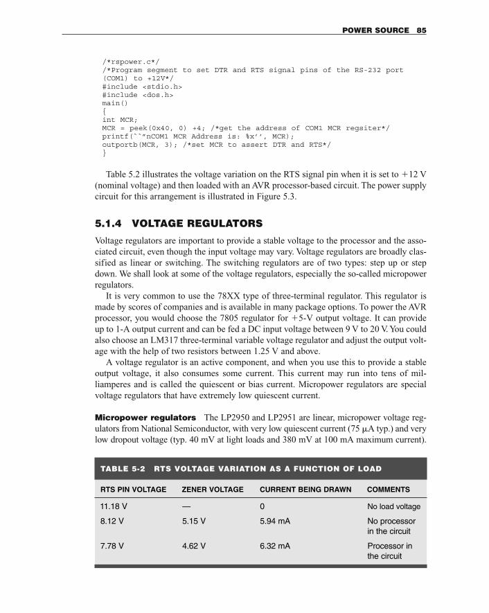
/*rspower.c*//*Program segment to set DTR and RTS signal pins of the RS-232 port(COM1) to +12V*/#include <stdio.h>#include <dos.h>main(){int MCR;MCR = peek(0x40, 0) +4; /*get the address of COM1 MCR regsiter*/printf(``”nCOM1 MCR Address is: %x’’, MCR);outportb(MCR, 3); /*set MCR to assert DTR and RTS*/}
Table 5.2 illustrates the voltage variation on the RTS signal pin when it is set to �12 V(nominal voltage) and then loaded with an AVR processor-based circuit. The power supplycircuit for this arrangement is illustrated in Figure 5.3.
5.1.4 VOLTAGE REGULATORS
Voltage regulators are important to provide a stable voltage to the processor and the asso-ciated circuit, even though the input voltage may vary. Voltage regulators are broadly clas-sified as linear or switching. The switching regulators are of two types: step up or stepdown. We shall look at some of the voltage regulators, especially the so-called micropowerregulators.
It is very common to use the 78XX type of three-terminal regulator. This regulator ismade by scores of companies and is available in many package options. To power the AVRprocessor, you would choose the 7805 regulator for �5-V output voltage. It can provideup to 1-A output current and can be fed a DC input voltage between 9 V to 20 V. You couldalso choose an LM317 three-terminal variable voltage regulator and adjust the output volt-age with the help of two resistors between 1.25 V and above.
A voltage regulator is an active component, and when you use this to provide a stableoutput voltage, it also consumes some current. This current may run into tens of mil-liamperes and is called the quiescent or bias current. Micropower regulators are specialvoltage regulators that have extremely low quiescent current.
Micropower regulators The LP2950 and LP2951 are linear, micropower voltage reg-ulators from National Semiconductor, with very low quiescent current (75 �A typ.) and verylow dropout voltage (typ. 40 mV at light loads and 380 mV at 100 mA maximum current).
POWER SOURCE 85
TABLE 5-2 RTS VOLTAGE VARIATION AS A FUNCTION OF LOAD
RTS PIN VOLTAGE ZENER VOLTAGE CURRENT BEING DRAWN COMMENTS
11.18 V — 0 No load voltage
8.12 V 5.15 V 5.94 mA No processor in the circuit
7.78 V 4.62 V 6.32 mA Processor in the circuit
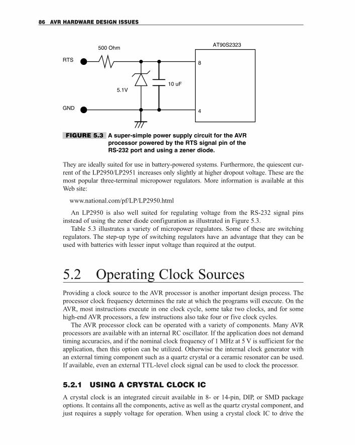
They are ideally suited for use in battery-powered systems. Furthermore, the quiescent cur-rent of the LP2950/LP2951 increases only slightly at higher dropout voltage. These are themost popular three-terminal micropower regulators. More information is available at thisWeb site:
www.national.com/pf/LP/LP2950.html
An LP2950 is also well suited for regulating voltage from the RS-232 signal pinsinstead of using the zener diode configuration as illustrated in Figure 5.3.
Table 5.3 illustrates a variety of micropower regulators. Some of these are switchingregulators. The step-up type of switching regulators have an advantage that they can beused with batteries with lesser input voltage than required at the output.
5.2 Operating Clock SourcesProviding a clock source to the AVR processor is another important design process. Theprocessor clock frequency determines the rate at which the programs will execute. On theAVR, most instructions execute in one clock cycle, some take two clocks, and for somehigh-end AVR processors, a few instructions also take four or five clock cycles.
The AVR processor clock can be operated with a variety of components. Many AVRprocessors are available with an internal RC oscillator. If the application does not demandtiming accuracies, and if the nominal clock frequency of 1 MHz at 5 V is sufficient for theapplication, then this option can be utilized. Otherwise the internal clock generator withan external timing component such as a quartz crystal or a ceramic resonator can be used.If available, even an external TTL-level clock signal can be used to clock the processor.
5.2.1 USING A CRYSTAL CLOCK IC
A crystal clock is an integrated circuit available in 8- or 14-pin, DIP, or SMD packageoptions. It contains all the components, active as well as the quartz crystal component, andjust requires a supply voltage for operation. When using a crystal clock IC to drive the
86 AVR HARDWARE DESIGN ISSUES
8
4
AT90S2323500 Ohm
5.1V10 uF
GND
RTS
FIGURE 5.3 A super-simple power supply circuit for the AVRprocessor powered by the RTS signal pin of theRS-232 port and using a zener diode.
clock input of the AVR processor, the clock signal is applied to the X1 input pin of the AVR processor.
The advantages of using a clock crystal IC are:
1. Industry standard package2. CMOS/TTL output3. 3.3-V operation available4. Large fanout capability
More details are available at this manufacturer’s Web site:
www.ndk.com/products/guide.htm
Figure 5.4 illustrates an 8-pin crystal clock and pinout.
5.2.2 USING A CERAMIC RESONATOR
For low-cost applications, a ceramic resonator is an attractive proposition. Ceramic res-onators are three terminal components with the resonant components in a single packageas illustrated in Figure 5.5.
Figure 5.6 illustrates how a ceramic resonator can be connected to the oscillator pins ofthe AVR processor. No other component is required for the oscillator.
The advantages of a ceramic resonator are:
1. Oscillation circuit does not require any additional capacitors2. Wide frequency range of resonators are available3. Small mechanical profile4. No external adjustment required
Typical operating characteristics of a ceramic resonator are:
1. Frequency range: 2.0 to 60 MHz2. Initial frequency tolerance: .5%3. Frequency Stability: .3%4. Frequency aging: .3% over 10 years’ time
OPERATING CLOCK SOURCES 87
TABLE 5-3 A SELECTION OF MICROPOWER VOLTAGE REGULATORS
COMPONENT V OUT QUIESCENT CURRENT COMMENTS
MAX667 1.3 V to 16 V 20 �A 8 pins, linear regulator
MAX639 5.0 V 10 �A 8 pins, switching regulator
MAX630 V in to 18 V 70 �A 8 pins, switching step-up regu-lator
LP2950-5.0 5.0 V 40 �A 3 pin, linear regulator
LP2980-5.0 5.0 V 65 �A 5 pin, ultralow dropout linearregulator
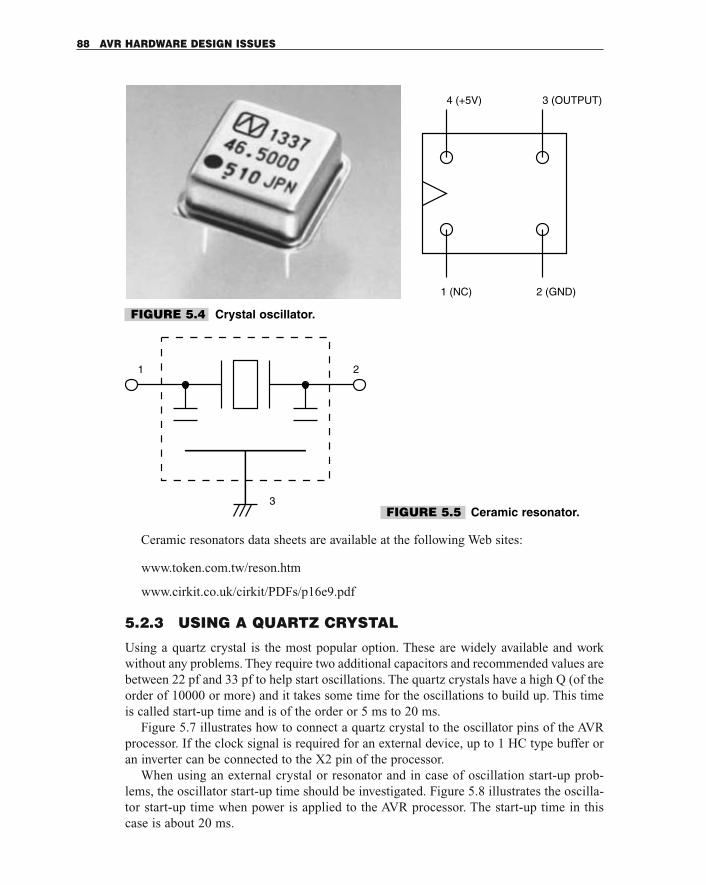
Ceramic resonators data sheets are available at the following Web sites:
www.token.com.tw/reson.htm
www.cirkit.co.uk/cirkit/PDFs/p16e9.pdf
5.2.3 USING A QUARTZ CRYSTAL
Using a quartz crystal is the most popular option. These are widely available and workwithout any problems. They require two additional capacitors and recommended values arebetween 22 pf and 33 pf to help start oscillations. The quartz crystals have a high Q (of theorder of 10000 or more) and it takes some time for the oscillations to build up. This timeis called start-up time and is of the order or 5 ms to 20 ms.
Figure 5.7 illustrates how to connect a quartz crystal to the oscillator pins of the AVRprocessor. If the clock signal is required for an external device, up to 1 HC type buffer oran inverter can be connected to the X2 pin of the processor.
When using an external crystal or resonator and in case of oscillation start-up prob-lems, the oscillator start-up time should be investigated. Figure 5.8 illustrates the oscilla-tor start-up time when power is applied to the AVR processor. The start-up time in thiscase is about 20 ms.
88 AVR HARDWARE DESIGN ISSUES
1 (NC) 2 (GND)
3 (OUTPUT)4 (+5V)
1 2
3
FIGURE 5.4 Crystal oscillator.
FIGURE 5.5 Ceramic resonator.
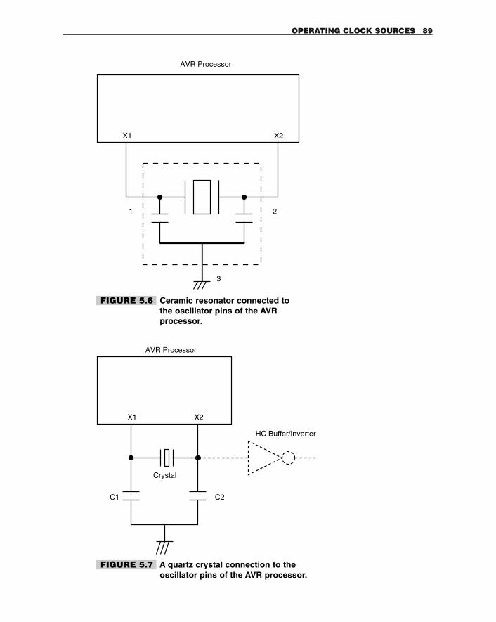
OPERATING CLOCK SOURCES 89
3
1 2
X1 X2
AVR Processor
FIGURE 5.6 Ceramic resonator connected tothe oscillator pins of the AVRprocessor.
X1 X2
AVR Processor
Crystal
HC Buffer/Inverter
C1 C2
FIGURE 5.7 A quartz crystal connection to theoscillator pins of the AVR processor.
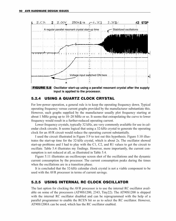
5.2.4 USING A QUARTZ CLOCK CRYSTAL
For low-power operation, a general rule is to keep the operating frequency down. Typicaloperating frequency versus current graphs provided by the manufacturer substantiate this.However, such graphs supplied by the manufacturer usually plot frequency starting atabout 1 MHz going up to 10–20 MHz or so. It seems that extrapolating the curve to lowerfrequency would result in a further-reduced operating current.
Lower frequency crystals, typically 32 kHz, are very commonly available for use in cal-endar clock circuits. It seems logical that using a 32-kHz crystal to generate the operatingclock for an AVR circuit would reduce the operating current substantially.
I used the circuit illustrated in Figure 5.9 to test out this hypothesis. Figure 5.10 illus-trates the start-up time for the 32-kHz crystal, which is about 2s. The oscillator showedstart-up problems and I had to play with the C1, C2, and R1 values to get the circuit tooscillate. Table 5.4 illustrates my findings. However, more importantly, the current con-sumption is not reduced at all, as illustrated in Table 5.4.
Figure 5.11 illustrates an oscilloscope screen shot of the oscillations and the dynamiccurrent consumption by the processor. The current consumption peaks during the timeswhen the oscillations are in a transition phase.
It is concluded that the 32-kHz calendar clock crystal is not a viable component to beused with the AVR processor in terms of current savings.
5.2.5 USING INTERNAL RC CLOCK OSCILLATOR
The last option for clocking the AVR processor is to use the internal RC oscillator avail-able on some of the processors (AT90S1200, 2343, Tiny22). The AT90S1200 is shippedwith the internal RC oscillator disabled and can be reprogrammed with the help of a parallel programmer to enable the RCEN bit so as to select the RC oscillator. However,AT90S1200A can be used, which has the RC oscillator enabled.
90 AVR HARDWARE DESIGN ISSUES
A regular parallel resonant crystal start-up time
Voltage input switched ON here
Stabilized oscillations
FIGURE 5.8 Oscillator start-up using a parallel resonant crystal after the supplyinput is applied to the processor.
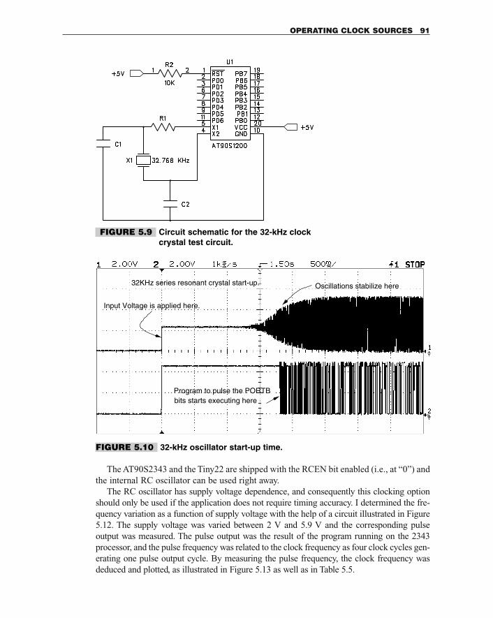
The AT90S2343 and the Tiny22 are shipped with the RCEN bit enabled (i.e., at “0”) andthe internal RC oscillator can be used right away.
The RC oscillator has supply voltage dependence, and consequently this clocking optionshould only be used if the application does not require timing accuracy. I determined the fre-quency variation as a function of supply voltage with the help of a circuit illustrated in Figure5.12. The supply voltage was varied between 2 V and 5.9 V and the corresponding pulse output was measured. The pulse output was the result of the program running on the 2343processor, and the pulse frequency was related to the clock frequency as four clock cycles gen-erating one pulse output cycle. By measuring the pulse frequency, the clock frequency wasdeduced and plotted, as illustrated in Figure 5.13 as well as in Table 5.5.
OPERATING CLOCK SOURCES 91
32KHz series resonant crystal start-up.
Input Voltage is applied here.
Oscillations stabilize here
Program to pulse the PORTBbits starts executing here
FIGURE 5.10 32-kHz oscillator start-up time.
FIGURE 5.9 Circuit schematic for the 32-kHz clockcrystal test circuit.
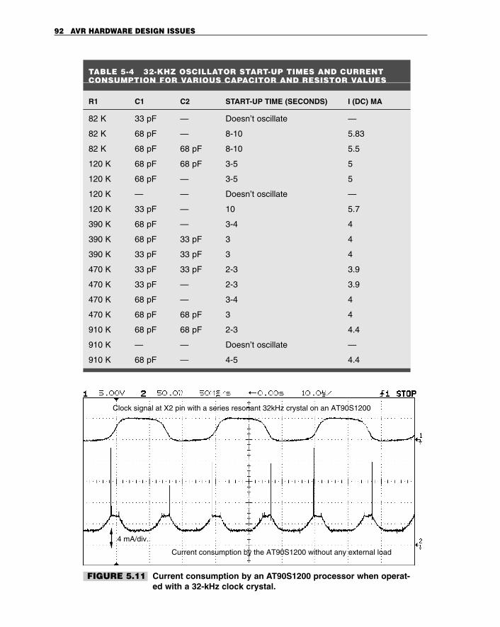
92 AVR HARDWARE DESIGN ISSUES
TABLE 5-4 32-KHZ OSCILLATOR START-UP TIMES AND CURRENT CONSUMPTION FOR VARIOUS CAPACITOR AND RESISTOR VALUES
R1 C1 C2 START-UP TIME (SECONDS) I (DC) MA
82 K 33 pF — Doesn’t oscillate —
82 K 68 pF — 8-10 5.83
82 K 68 pF 68 pF 8-10 5.5
120 K 68 pF 68 pF 3-5 5
120 K 68 pF — 3-5 5
120 K — — Doesn’t oscillate —
120 K 33 pF — 10 5.7
390 K 68 pF — 3-4 4
390 K 68 pF 33 pF 3 4
390 K 33 pF 33 pF 3 4
470 K 33 pF 33 pF 2-3 3.9
470 K 33 pF — 2-3 3.9
470 K 68 pF — 3-4 4
470 K 68 pF 68 pF 3 4
910 K 68 pF 68 pF 2-3 4.4
910 K — — Doesn’t oscillate —
910 K 68 pF — 4-5 4.4
Clock signal at X2 pin with a series resonant 32kHz crystal on an AT90S1200
Current consumption by the AT90S1200 without any external load
4 mA/div.
FIGURE 5.11 Current consumption by an AT90S1200 processor when operat-ed with a 32-kHz clock crystal.
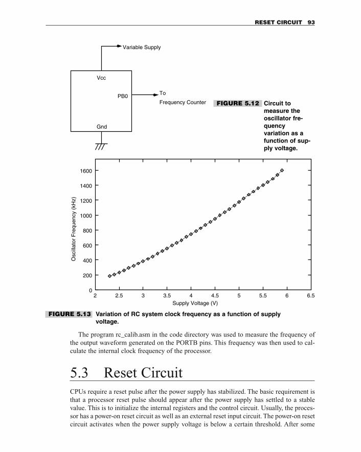
The program rc_calib.asm in the code directory was used to measure the frequency ofthe output waveform generated on the PORTB pins. This frequency was then used to cal-culate the internal clock frequency of the processor.
5.3 Reset CircuitCPUs require a reset pulse after the power supply has stabilized. The basic requirement isthat a processor reset pulse should appear after the power supply has settled to a stablevalue. This is to initialize the internal registers and the control circuit. Usually, the proces-sor has a power-on reset circuit as well as an external reset input circuit. The power-on resetcircuit activates when the power supply voltage is below a certain threshold. After some
RESET CIRCUIT 93
PB0
Vcc
Variable Supply
Gnd
To
Frequency Counter FIGURE 5.12 Circuit to measure theoscillator fre-quency variation as afunction of sup-ply voltage.
Supply Voltage (V)
Osc
illat
or F
requ
ency
(kH
z)
600
800
1000
1200
1400
1600
2 2.5
400
30
3.5 4 4.5 5 5.5 6 6.5
200
FIGURE 5.13 Variation of RC system clock frequency as a function of supplyvoltage.
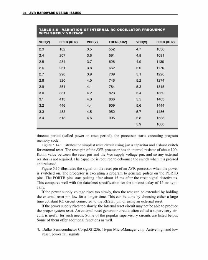
timeout period (called power-on reset period), the processor starts executing programmemory code.
Figure 5.14 illustrates the simplest reset circuit using just a capacitor and a shunt switchfor external reset. The reset pin of the AVR processor has an internal resistor of about 100-Kohm value between the reset pin and the Vcc supply voltage pin, and so any externalresistor is not required. The capacitor is required to debounce the switch when it is pressedand released.
Figure 5.15 illustrates the signal on the reset pin of an AVR processor when the poweris switched on. The processor is executing a program to generate pulses on the PORTBpins. The PORTB pins start pulsing after about 15 ms after the reset signal deactivates.This compares well with the datasheet specification for the timeout delay of 16 ms typi-cally.
If the power supply voltage rises too slowly, then the rest can be extended by holdingthe external reset pin low for a longer time. This can be done by choosing either a largetime constant RC circuit connected to the RESET pin or using an external reset.
If the power supply rises too slowly, the internal reset circuit may not be able to producethe proper system reset. An external reset generator circuit, often called a supervisory cir-cuit, is useful for such needs. Some of the popular supervisory circuits are listed below.Some of them offer additional functions as well.
1. Dallas Semiconductor Corp:DS1236. 16-pin MicroManager chip. Active high and lowreset, power fail signals.
94 AVR HARDWARE DESIGN ISSUES
TABLE 5-5 VARIATION OF INTERNAL RC OSCILLATOR FREQUENCY WITH SUPPLY VOLTAGE
VCC(V) FREQ (KHZ) VCC(V) FREQ (KHZ) VCC(V) FREQ (KHZ)
2.3 182 3.5 552 4.7 1036
2.4 207 3.6 591 4.8 1081
2.5 234 3.7 628 4.9 1130
2.6 261 3.8 662 5.0 1176
2.7 290 3.9 709 5.1 1226
2.8 320 4.0 746 5.2 1274
2.9 351 4.1 784 5.3 1315
3.0 381 4.2 823 5.4 1360
3.1 413 4.3 866 5.5 1403
3.2 446 4.4 909 5.6 1444
3.3 483 4.5 952 5.7 1486
3.4 518 4.6 995 5.8 1538
5.9 1600
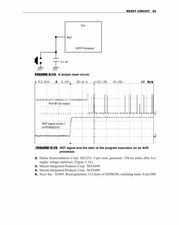
2. Dallas Semiconductor Corp: DS1233. 3-pin reset generator. 350-ms pulse after Vccsupply voltage stabilizes. (Figure 5.16.)
3. Maxim Integrated Products Corp: MAX6904. Maxim Integrated Products Corp: MAX8095. Xicor Inc: X5045. Reset generator, 512 bytes of EEPROM, watchdog timer. 8-pin DIP.
RESET CIRCUIT 95
RST
Vcc
AVR Processor
0.1 uF
FIGURE 5.14 A simple reset circuit.
Port B7 as output
RST signal on pin 1of AT90S2313
FIGURE 5.15 RST signal and the start of the program execution on an AVRprocessor.
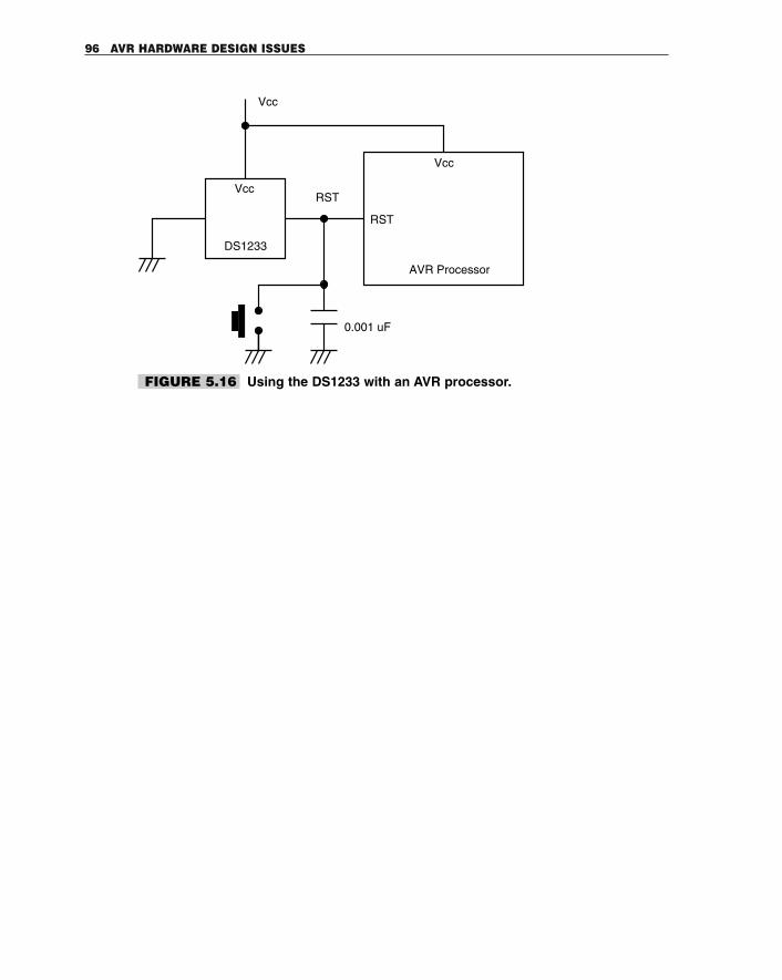
96 AVR HARDWARE DESIGN ISSUES
RST
RST
Vcc
Vcc
DS1233
Vcc
0.001 uF
AVR Processor
FIGURE 5.16 Using the DS1233 with an AVR processor.
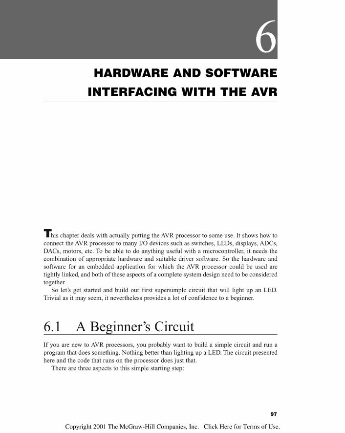
This chapter deals with actually putting the AVR processor to some use. It shows how toconnect the AVR processor to many I/O devices such as switches, LEDs, displays, ADCs,DACs, motors, etc. To be able to do anything useful with a microcontroller, it needs thecombination of appropriate hardware and suitable driver software. So the hardware andsoftware for an embedded application for which the AVR processor could be used aretightly linked, and both of these aspects of a complete system design need to be consideredtogether.
So let’s get started and build our first supersimple circuit that will light up an LED.Trivial as it may seem, it nevertheless provides a lot of confidence to a beginner.
6.1 A Beginner’s CircuitIf you are new to AVR processors, you probably want to build a simple circuit and run aprogram that does something. Nothing better than lighting up a LED. The circuit presentedhere and the code that runs on the processor does just that.
There are three aspects to this simple starting step:
6HARDWARE AND SOFTWARE
INTERFACING WITH THE AVR
97
Copyright 2001 The McGraw-Hill Companies, Inc. Click Here for Terms of Use.
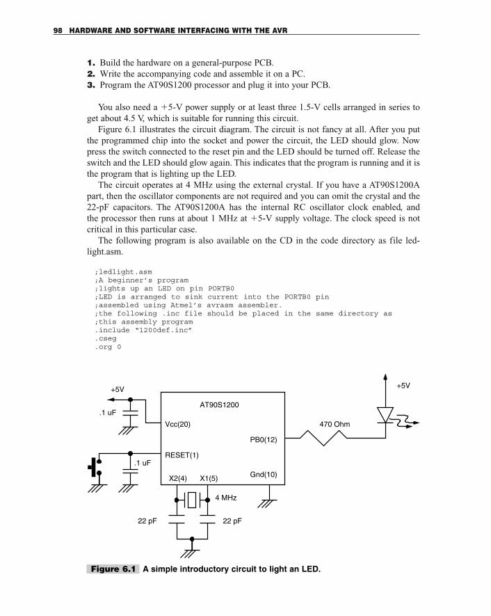
1. Build the hardware on a general-purpose PCB.2. Write the accompanying code and assemble it on a PC.3. Program the AT90S1200 processor and plug it into your PCB.
You also need a �5-V power supply or at least three 1.5-V cells arranged in series toget about 4.5 V, which is suitable for running this circuit.
Figure 6.1 illustrates the circuit diagram. The circuit is not fancy at all. After you putthe programmed chip into the socket and power the circuit, the LED should glow. Nowpress the switch connected to the reset pin and the LED should be turned off. Release theswitch and the LED should glow again. This indicates that the program is running and it isthe program that is lighting up the LED.
The circuit operates at 4 MHz using the external crystal. If you have a AT90S1200Apart, then the oscillator components are not required and you can omit the crystal and the22-pF capacitors. The AT90S1200A has the internal RC oscillator clock enabled, and the processor then runs at about 1 MHz at �5-V supply voltage. The clock speed is notcritical in this particular case.
The following program is also available on the CD in the code directory as file led-light.asm.
;ledlight.asm;A beginner’s program;lights up an LED on pin PORTB0;LED is arranged to sink current into the PORTB0 pin;assembled using Atmel’s avrasm assembler.;the following .inc file should be placed in the same directory as;this assembly program.include “1200def.inc”.cseg.org 0
98 HARDWARE AND SOFTWARE INTERFACING WITH THE AVR
+5V
470 Ohm
PB0(12)
AT90S1200
Vcc(20)
RESET(1)
Gnd(10)
22 pF22 pF
4 MHz
.1 uF
+5V
.1 uF
X2(4) X1(5)
Figure 6.1 A simple introductory circuit to light an LED.
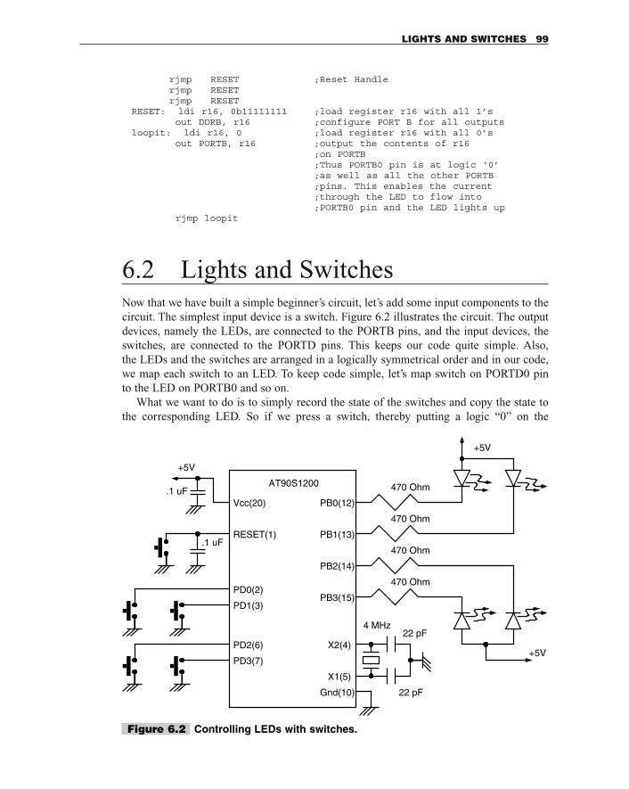
rjmp RESET ;Reset Handlerjmp RESETrjmp RESET
RESET: ldi r16, 0b11111111 ;load register r16 with all 1’sout DDRB, r16 ;configure PORT B for all outputs
loopit: ldi r16, 0 ;load register r16 with all 0’sout PORTB, r16 ;output the contents of r16
;on PORTB;Thus PORTB0 pin is at logic ‘0’;as well as all the other PORTB;pins. This enables the current;through the LED to flow into;PORTB0 pin and the LED lights up
rjmp loopit
6.2 Lights and SwitchesNow that we have built a simple beginner’s circuit, let’s add some input components to thecircuit. The simplest input device is a switch. Figure 6.2 illustrates the circuit. The outputdevices, namely the LEDs, are connected to the PORTB pins, and the input devices, theswitches, are connected to the PORTD pins. This keeps our code quite simple. Also, the LEDs and the switches are arranged in a logically symmetrical order and in our code,we map each switch to an LED. To keep code simple, let’s map switch on PORTD0 pin to the LED on PORTB0 and so on.
What we want to do is to simply record the state of the switches and copy the state tothe corresponding LED. So if we press a switch, thereby putting a logic “0” on the
LIGHTS AND SWITCHES 99
AT90S1200
Vcc(20)
RESET(1).1 uF
+5V
.1 uF
Gnd(10)
470 Ohm
+5V
470 Ohm
470 Ohm
470 Ohm
+5V
22 pF4 MHz
22 pF
PB0(12)
PB1(13)
PB2(14)
PB3(15)PD0(2)
PD1(3)
PD2(6)
PD3(7)
X2(4)
X1(5)
Figure 6.2 Controlling LEDs with switches.
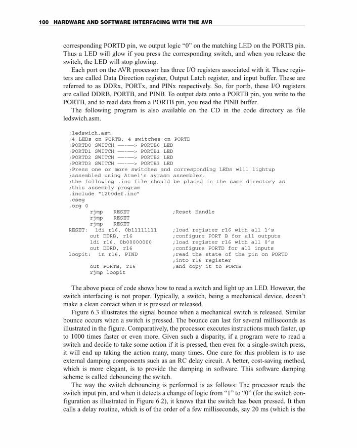
corresponding PORTD pin, we output logic “0” on the matching LED on the PORTB pin.Thus a LED will glow if you press the corresponding switch, and when you release theswitch, the LED will stop glowing.
Each port on the AVR processor has three I/O registers associated with it. These regis-ters are called Data Direction register, Output Latch register, and input buffer. These arereferred to as DDRx, PORTx, and PINx respectively. So, for portb, these I/O registers are called DDRB, PORTB, and PINB. To output data onto a PORTB pin, you write to thePORTB, and to read data from a PORTB pin, you read the PINB buffer.
The following program is also available on the CD in the code directory as fileledswich.asm.
;ledswich.asm;4 LEDs on PORTB, 4 switches on PORTD;PORTD0 SWITCH ——-——> PORTB0 LED;PORTD1 SWITCH ——-——> PORTB1 LED;PORTD2 SWITCH ——-——> PORTB2 LED;PORTD3 SWITCH ——-——> PORTB3 LED;Press one or more switches and corresponding LEDs will lightup;assembled using Atmel’s avrasm assembler.;the following .inc file should be placed in the same directory as;this assembly program.include “1200def.inc”.cseg.org 0
rjmp RESET ;Reset Handlerjmp RESETrjmp RESET
RESET: ldi r16, 0b11111111 ;load register r16 with all 1’sout DDRB, r16 ;configure PORT B for all outputsldi r16, 0b00000000 ;load register r16 with all 0’sout DDRD, r16 ;configure PORTD for all inputs
loopit: in r16, PIND ;read the state of the pin on PORTD;into r16 register
out PORTB, r16 ;and copy it to PORTBrjmp loopit
The above piece of code shows how to read a switch and light up an LED. However, theswitch interfacing is not proper. Typically, a switch, being a mechanical device, doesn’tmake a clean contact when it is pressed or released.
Figure 6.3 illustrates the signal bounce when a mechanical switch is released. Similarbounce occurs when a switch is pressed. The bounce can last for several milliseconds asillustrated in the figure. Comparatively, the processor executes instructions much faster, upto 1000 times faster or even more. Given such a disparity, if a program were to read aswitch and decide to take some action if it is pressed, then even for a single-switch press,it will end up taking the action many, many times. One cure for this problem is to useexternal damping components such as an RC delay circuit. A better, cost-saving method,which is more elegant, is to provide the damping in software. This software dampingscheme is called debouncing the switch.
The way the switch debouncing is performed is as follows: The processor reads theswitch input pin, and when it detects a change of logic from “1” to “0” (for the switch con-figuration as illustrated in Figure 6.2), it knows that the switch has been pressed. It thencalls a delay routine, which is of the order of a few milliseconds, say 20 ms (which is the
100 HARDWARE AND SOFTWARE INTERFACING WITH THE AVR
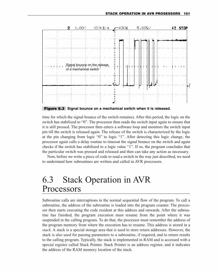
time for which the signal bounce of the switch remains). After this period, the logic on theswitch has stabilized to “0”. The processor then reads the switch input again to ensure thatit is still pressed. The processor then enters a software loop and monitors the switch inputpin till the switch is released again. The release of the switch is characterized by the logicat the pin changing from logic “0” to logic “1”. After detecting this logic change, theprocessor again calls a delay routine to timeout the signal bounce on the switch and againchecks if the switch has stabilized to a logic value “1”. If so, the program concludes thatthe particular switch was pressed and released and then can take any action as necessary.
Now, before we write a piece of code to read a switch in the way just described, we needto understand how subroutines are written and called in AVR processors.
6.3 Stack Operation in AVR ProcessorsSubroutine calls are interruptions in the normal sequential flow of the program. To call asubroutine, the address of the subroutine is loaded into the program counter. The proces-sor then starts executing the code resident at this address and onwards. After the subrou-tine has finished, the program execution must resume from the point where it was suspended in the calling program. To do that, the processor must remember the address ofthe program memory from where the execution has to resume. This address is stored in astack. A stack is a special storage area that is used to store return addresses. However, thestack is also used for passing parameters to a subroutine, if required, and to return resultsto the calling program. Typically, the stack is implemented in RAM and is accessed with aspecial register called Stack Pointer. Stack Pointer is an address register, and it indicatesthe address of the RAM memory location of the stack.
STACK OPERATION IN AVR PROSESSORS 101
Signal bounce on the releaseof a mechanical switch
Figure 6.3 Signal bounce on a mechanical switch when it is released.
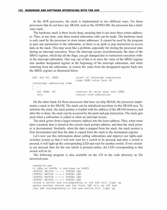
In the AVR processors, the stack is implemented in two different ways. For thoseprocessors that do not have any SRAM, such as the AT90S1200, the processor has a hard-ware stack.
The hardware stack is three levels deep, meaning that it can store three return address-es. Thus, at any time, only three nested subroutine calls can be made. The hardware stackis only used by the processor to store return addresses. It cannot be used by the programto pass any parameters to the subroutine, as there is no push or pop instruction to accessdata on the stack. This may seem like a problem, especially for storing the processor stateduring an interrupt execution. Since the interrupt occurs asynchronously, the state of theSREG register, which has all the flags, can get changed due to instruction execution with-in the interrupt subroutine. One way out of this is to store the value of the SREG registerinto another designated register at the beginning of the interrupt subroutine, and whilereturning from the subroutine, to restore the value from the designated register back intothe SREG register as illustrated below.
ISR: mov R0, SREG ;start of interrupt subroutine;copy SREG value into R0
;Interrupt subroutine code; ....; ....
mov SREG, R0 ;restore R0 value back into SREGreti ;return from subroutine
On the other hand, for those processors that have on-chip SRAM, the processor imple-ments a stack in the SRAM. The stack can be initialized anywhere in this SRAM area. Toinitialize the stack, the stack pointer is loaded with the address of the SRAM memory, andafter this is done, the stack can be accessed by the push and pop instruction. The stack getsused when a subroutine is called or when an interrupt occurs.
The stack grows from a larger memory address into the lower address. Thus, when somedata is pushed, data is stored at the current stack pointer address, and then the stack point-er is decremented. Similarly, when the data is popped from the stack, the stack pointer isfirst incremented and then the data is copied from the stack to the destination register.
Let’s now use this information about calling subroutines and improve our lights-and-switches system so that it will now wait for a switch to be pressed, and after a switch ispressed, it will light up the corresponding LED and wait for another switch. If two switch-es are pressed, then for the one which is pressed earlier, the LED corresponding to thatswitch will be lit.
The following program is also available on the CD in the code directory as filenewswich.asm.
;newswich.asm;4 LEDs on PORTB, 4 switches on PORTD;PORTD0 SWITCH ——-——> PORTB0 LED;PORTD1 SWITCH ——-——> PORTB1 LED;PORTD2 SWITCH ——-——> PORTB2 LED;PORTD3 SWITCH ——-——> PORTB3 LED;Press a switch and corresponding to the LED will light up;press another switch and the first LED will go off and;the LED corresponding to the new switch will light up
102 HARDWARE AND SOFTWARE INTERFACING WITH THE AVR
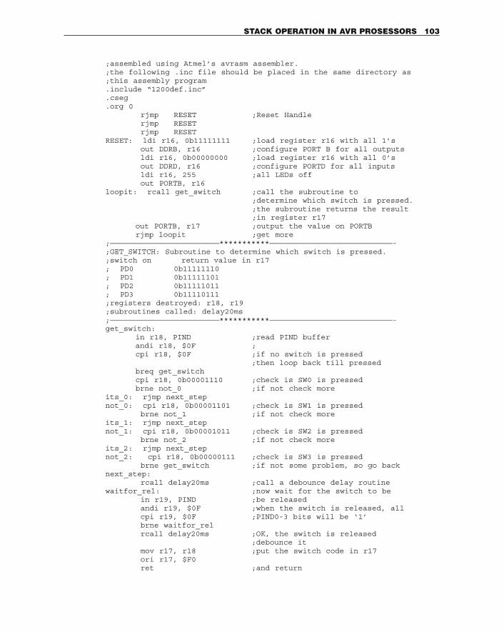
;assembled using Atmel’s avrasm assembler.;the following .inc file should be placed in the same directory as;this assembly program.include “1200def.inc”.cseg.org 0
rjmp RESET ;Reset Handlerjmp RESETrjmp RESET
RESET: ldi r16, 0b11111111 ;load register r16 with all 1’sout DDRB, r16 ;configure PORT B for all outputsldi r16, 0b00000000 ;load register r16 with all 0’sout DDRD, r16 ;configure PORTD for all inputsldi r16, 255 ;all LEDs offout PORTB, r16
loopit: rcall get_switch ;call the subroutine to;determine which switch is pressed.;the subroutine returns the result;in register r17
out PORTB, r17 ;output the value on PORTBrjmp loopit ;get more
;————————————————————————***********———————————————————————————-;GET_SWITCH: Subroutine to determine which switch is pressed.;switch on return value in r17; PD0 0b11111110; PD1 0b11111101; PD2 0b11111011; PD3 0b11110111;registers destroyed: r18, r19;subroutines called: delay20ms;————————————————————————***********———————————————————————————-get_switch:
in r18, PIND ;read PIND bufferandi r18, $0F ;cpi r18, $0F ;if no switch is pressed
;then loop back till pressedbreq get_switchcpi r18, 0b00001110 ;check is SW0 is pressedbrne not_0 ;if not check more
its_0: rjmp next_stepnot_0: cpi r18, 0b00001101 ;check is SW1 is pressed
brne not_1 ;if not check moreits_1: rjmp next_stepnot_1: cpi r18, 0b00001011 ;check is SW2 is pressed
brne not_2 ;if not check moreits_2: rjmp next_stepnot_2: cpi r18, 0b00000111 ;check is SW3 is pressed
brne get_switch ;if not some problem, so go backnext_step:
rcall delay20ms ;call a debounce delay routinewaitfor_rel: ;now wait for the switch to be
in r19, PIND ;be releasedandi r19, $0F ;when the switch is released, allcpi r19, $0F ;PIND0-3 bits will be ‘1’brne waitfor_relrcall delay20ms ;OK, the switch is released
;debounce itmov r17, r18 ;put the switch code in r17ori r17, $F0ret ;and return
STACK OPERATION IN AVR PROSESSORS 103
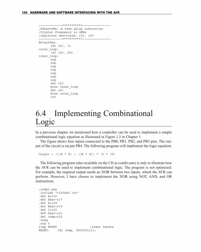
;————————————***********———————————————-;DELAY20MS: A 20ms delay subroutine;Crystal Frequency is 4MHz;registers destroyed: r21, r20;————————————***********———————————————-delay20ms:
ldi r21, 31outer_loop:
ldi r20, 255inner_loop:
nopnopnopnopnopnopnopdec r20brne inner_loopdec r21brne outer_loopret
6.4 Implementing CombinationalLogicIn a previous chapter we mentioned how a controller can be used to implement a simplecombinational logic equation as illustrated in Figure 1.3 in Chapter 1.
The figure shows four inputs connected to the PB0, PB1, PB2, and PB3 pins. The out-put of the circuit is on pin PB4. The following program will implement the logic equation:
Output = ((/A * B) + (/B * A)) * (C * /D)
The following program (also available on the CD as combi.asm) is only to illustrate howthe AVR can be used to implement combinational logic. The program is not optimized. For example, the required output needs an XOR between two inputs, which the AVR can perform. However, I have chosen to implement the XOR using NOT, AND, and OR instructions.
;combi.asm.include “1200def.inc”.def A=r16.def Abar=r17.def B=r18.def Bbar=r19.def C=r20.def Dbar=r21.def temp=r22.cseg.org 0rjmp RESET ;reset handleRESET: ldi temp, 0b00001111;
104 HARDWARE AND SOFTWARE INTERFACING WITH THE AVR
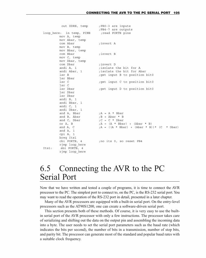
out DDRB, temp ;PB0-3 are inputs;PB4-7 are outputs
loop_here: in temp, PINB ;read PORTB pinsmov A, tempmov Abar, tempcom Abar ;invert Amov B, tempmov Bbar, tempcom Bbar ;invert Bmov C, tempmov Dbar, tempcom Dbar ;invert Dandi A, 1 ;isolate the bit for Aandi Abar, 1 ;isolate the bit for Abarlsr B ;get input B to position bit0lsr Bbarlsr C ;get input C to position bit0lsr Clsr Dbar ;get input D to position bit0lsr Dbarlsr Dbarandi B, 1andi Bbar, 1andi C, 1andi Dbar, 1and A, Bbar ;A = A * Bbarand B, Abar ;B = Abar * Band C, Dbar ;C = C * Dbaror A, B ;A = (A * Bbar) + (Abar * B)and A, C ;A = ((A * Bbar) + (Abar * B))* (C * Dbar)and A, 1cpi A, 1breq Its1cbi PORTB, 4 ;no its 0, so reset PB4rjmp loop_here
Its1: sbi PORTB, 4rjmp loop_here
6.5 Connecting the AVR to the PCSerial PortNow that we have written and tested a couple of programs, it is time to connect the AVRprocessor to the PC. The simplest port to connect to, on the PC, is the RS-232 serial port. Youmay want to read the operation of the RS-232 port in detail, presented in a later chapter.
Many of the AVR processors are equipped with a built-in serial port. On the entry-levelprocessors such as the AT90S1200, one can create a software-driven serial port.
This section presents both of these methods. Of course, it is very easy to use the built-in serial port of the AVR processor with only a few instructions. The processor takes careof serializing and shifting out the data on the output pin and assembling the incoming datainto a byte. The user needs to set the serial port parameters such as the baud rate (whichindicates the bits per second), the number of bits in a transmission, number of stop bits,and parity bit. The processor can generate most of the standard and popular baud rates witha suitable clock frequency.
CONNECTING THE AVR TO THE PC SERIAL PORT 105
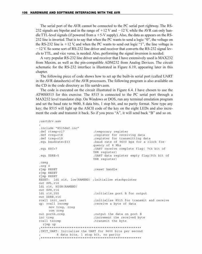
The serial port of the AVR cannot be connected to the PC serial port rightway. The RS-232 signals are bipolar and in the range of �12 V and �12 V, while the AVR can only han-dle TTL-level signals (if powered from a �5-V supply). Also, the data as appears on the RS-232 line is inverted. That is to say that when the PC wants to send a logic “0”, the voltage onthe RS-232 line is �12 V, and when the PC wants to send out logic “1”, the line voltage is�12 V. So some sort of RS-232 line driver and receiver that converts the RS-232 signal lev-els to TTL, and vice versa, is needed. Also, performing the signal inversion is needed.
A very popular RS-232 line driver and receiver that I have extensively used is MAX232from Maxim, as well as the pin-compatible ADM232 from Analog Devices. The circuitschematic for the RS-232 interface is illustrated in Figure 6.19, appearing later in thischapter.
The following piece of code shows how to set up the built-in serial port (called UARTin the AVR datasheets) of the AVR processors. The following program is also available onthe CD in the code directory as file uartdrv.asm.
The code is executed on the circuit illustrated in Figure 6.4. I have chosen to use theAT90S8515 for this exercise. The 8515 is connected to the PC serial port through aMAX232 level translator chip. On Windows or DOS, run any terminal emulation programand set the baud rate to 9600, 8 data bits, 1 stop bit, and no parity format. Now type anykey; the 8515 will light up the ASCII code of the key on the eight LEDs and also incre-ment the code and transmit it back. So if you press “A”, it will send back “B” and so on.
;uartdrv.asm;.include “8515def.inc”.def rtemp=r17 ;temporary register.def rreg=r18 ;register for receiving data.def treg=r19 ;register for transmitting data.equ baudrate=$33 ;baud rate of 9600 bps for a clock fre-
quency of 8 Mhz.equ RXC=7 ;UART receive complete flag( 7th bit of
USR register).equ UDRE=5 ;UART data register empty flag(5th bit of
USR register).cseg.org 0rjmp RESET ;reset handlerjmp RESETrjmp RESETRESET: ldi r16, low(RAMEND) ;initialize stackpointerout SPL,r16ldi r16, HIGH(RAMEND)out SPH,r16ldi r16,255 ;initialize port B for outputout DDRB,r16rcall init_uart ;initialize 8515 for transmit and receiveup: rcall rxcomp ;receive a byte of data
mov treg, rregcom rreg
out portb,rreg ;output the data on port Binc treg ;increment the received bytercall txcomp ;transmit the byte
rjmp up;*******************************************************;INIT_UART: Initialize the UART for 9600 bits per second; 8 data bits, 1 stop bit, no parity;*******************************************************
106 HARDWARE AND SOFTWARE INTERFACING WITH THE AVR
.1 uF
+5V
.1 uF
22 pF
22 pF
8 MHz
+5VAT90S8515
PB0(1)
PB1(2)
PB2(3)
PB3(4)
PB4(5)
PB5(6)
PB6(7)
PB7(8)
Gnd(20)
Vcc(40)
RESET(9)
X2(18)
X1(19)
TxD(11)
RxD(10)
MAX232
PC TxD
PC RxD
1 KOhm
Figure 6.4 Connecting AT90S8515 to a PC serial port. Other components that go with MAX232 are not illustrated.
10
7
init_uart:ldi rtemp, baudrate ;set baud rateout UBRR,rtempldi rtemp, $18 ;initialize UART control registerout UCR, rtempret
;*******************************************************;RXCOMP: Receive a byte from the serial port;polls the RXC flag in the UART Status Reg (USR);if ‘1’, then data is read from the UART Data Register (UDR);*******************************************************rxcomp: sbis USR,RXC ;poll to check if char received
rjmp rxcompin rreg,UDR ;put received data in rregret
;*******************************************************;TXCOMP: Transmit a byte from the serial port;polls to see if the UDRE flag is ‘1’. If ‘1’ then;a byte is written to the UDR to be transmitted.;*******************************************************txcomp: sbis USR,UDRE ;poll to check end of transmission
rjmp txcompout UDR, tregret
For those processors that do not have a built-in UART, we describe a software-drivenserial port. A software-driven serial port can only be half duplex, meaning that either theserial data can be received or it can be transmitted. A hardware UART, on the other hand,can be full duplex, as the data transmission and reception are being handled by hardwareregisters that do not need any program intervention in the actual bit-shifting process.
Figure 6.5 illustrates the timing involved in a RS-232 transmission. To receive a serialbit stream, the program must monitor the signal (the TTL signal as illustrated in the fig-ure). The idle state of the serial TTL signal is “1”. As soon as a low-going transition isdetected, it denotes the beginning of the Start bit and the start of a transmission. The pro-gram just monitors the signal again at T/2 time later, which is denoted as the 0th sample.T denotes the bit time. For a 2400-bps speed, the bit time T � 1 2400, which is about 416us. Thus after ensuring that the signal is still “0”, the program then just samples the TTLsignal at each T time interval after the 0th sample at sample points denoted by 1, 2, 3, etc.The program just records the logic at these sample intervals and shifts the recorded logicvalues in a register. At the end of eight sample points, the data byte is ready.
Serial data transmission is easy compared to receiving it. The program just generates astart bit for T time units and then shifts out the data to be transmitted, each bit lasting Ttime units. To get the timing intervals, the AVR processor can use the Timer0 timer, whichis available in all the AVR processors.
The software-driven data transmission and reception routine that is included on the CDin fact interfaces directly to the RS-232 port without using any MAX232 type of line con-verters. The level conversion from RS-232 level to TTL is performed with a few resistorsand diodes. The signal inversion is performed in software. For transmission, the TTL datacan be directly put on a RS-232 line, and the PC will receive it correctly (the data must beinverted in logic, though).
A working example of this approach is illustrated in a later chapter, and the circuit dia-gram is illustrated in Figure 17.7. Serial driver (bit-banging method) test code for Figure17.7 is available in the code directory in file ser_drv.asm.
108 HARDWARE AND SOFTWARE INTERFACING WITH THE AVR
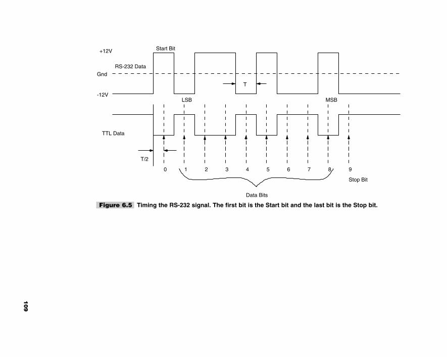
-12V
+12V
Gnd
TTL Data
RS-232 Data
T
1 2 3 4 5 6 7 8 9
T/2
Start Bit
0
Data Bits
Stop Bit
LSB MSB
Figure 6.5 Timing the RS-232 signal. The first bit is the Start bit and the last bit is the Stop bit.
10
9
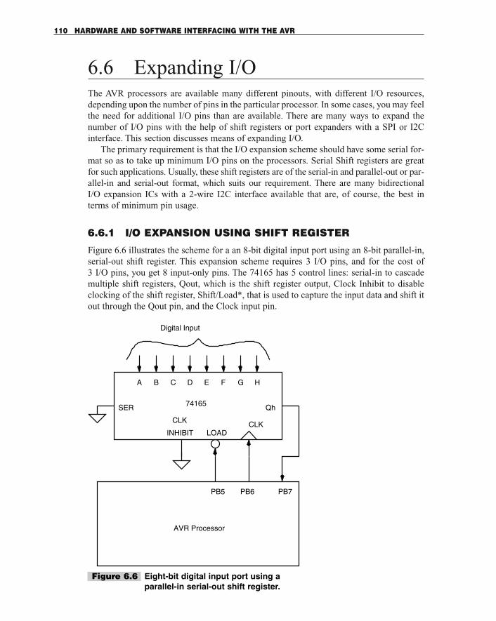
6.6 Expanding I/OThe AVR processors are available many different pinouts, with different I/O resources,depending upon the number of pins in the particular processor. In some cases, you may feelthe need for additional I/O pins than are available. There are many ways to expand thenumber of I/O pins with the help of shift registers or port expanders with a SPI or I2Cinterface. This section discusses means of expanding I/O.
The primary requirement is that the I/O expansion scheme should have some serial for-mat so as to take up minimum I/O pins on the processors. Serial Shift registers are greatfor such applications. Usually, these shift registers are of the serial-in and parallel-out or par-allel-in and serial-out format, which suits our requirement. There are many bidirectionalI/O expansion ICs with a 2-wire I2C interface available that are, of course, the best interms of minimum pin usage.
6.6.1 I/O EXPANSION USING SHIFT REGISTER
Figure 6.6 illustrates the scheme for a an 8-bit digital input port using an 8-bit parallel-in,serial-out shift register. This expansion scheme requires 3 I/O pins, and for the cost of 3 I/O pins, you get 8 input-only pins. The 74165 has 5 control lines: serial-in to cascademultiple shift registers, Qout, which is the shift register output, Clock Inhibit to disableclocking of the shift register, Shift/Load*, that is used to capture the input data and shift itout through the Qout pin, and the Clock input pin.
110 HARDWARE AND SOFTWARE INTERFACING WITH THE AVR
CLK
F G HEA B C D
74165 QhSER
INHIBIT
CLK
LOAD
Digital Input
AVR Processor
PB5 PB6 PB7
Figure 6.6 Eight-bit digital input port using aparallel-in serial-out shift register.
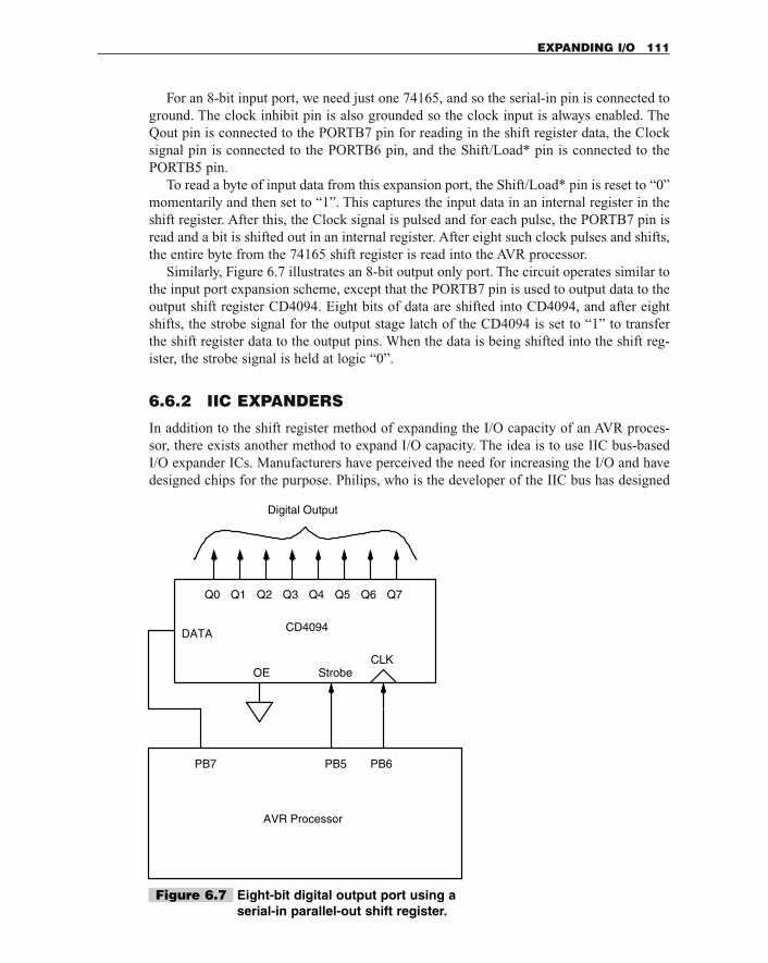
For an 8-bit input port, we need just one 74165, and so the serial-in pin is connected toground. The clock inhibit pin is also grounded so the clock input is always enabled. TheQout pin is connected to the PORTB7 pin for reading in the shift register data, the Clocksignal pin is connected to the PORTB6 pin, and the Shift/Load* pin is connected to thePORTB5 pin.
To read a byte of input data from this expansion port, the Shift/Load* pin is reset to “0”momentarily and then set to “1”. This captures the input data in an internal register in theshift register. After this, the Clock signal is pulsed and for each pulse, the PORTB7 pin isread and a bit is shifted out in an internal register. After eight such clock pulses and shifts,the entire byte from the 74165 shift register is read into the AVR processor.
Similarly, Figure 6.7 illustrates an 8-bit output only port. The circuit operates similar tothe input port expansion scheme, except that the PORTB7 pin is used to output data to theoutput shift register CD4094. Eight bits of data are shifted into CD4094, and after eightshifts, the strobe signal for the output stage latch of the CD4094 is set to “1” to transferthe shift register data to the output pins. When the data is being shifted into the shift reg-ister, the strobe signal is held at logic “0”.
6.6.2 IIC EXPANDERS
In addition to the shift register method of expanding the I/O capacity of an AVR proces-sor, there exists another method to expand I/O capacity. The idea is to use IIC bus-basedI/O expander ICs. Manufacturers have perceived the need for increasing the I/O and havedesigned chips for the purpose. Philips, who is the developer of the IIC bus has designed
EXPANDING I/O 111
CLK
AVR Processor
Digital Output
Strobe
CD4094
PB5 PB6
Q0 Q1 Q2 Q3 Q4 Q5 Q6 Q7
OE
DATA
PB7
Figure 6.7 Eight-bit digital output port using aserial-in parallel-out shift register.
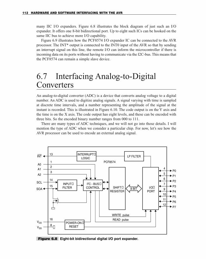
many IIC I/O expanders. Figure 6.8 illustrates the block diagram of just such an I/Oexpander. It offers one 8-bit bidirectional port. Up to eight such ICs can be hooked on thesame IIC bus to achieve more I/O capability.
Figure 6.9 illustrates how the PCF8574 I/O expander IC can be connected to the AVRprocessor. The INT* output is connected to the INT0 input of the AVR so that by sendingan interrupt signal on this line, the remote I/O can inform the microcontroller if there isincoming data on its ports without having to communicate via the I2C-bus. This means thatthe PCF8574 can remain a simple slave device.
6.7 Interfacing Analog-to-DigitalConvertersAn analog-to-digital converter (ADC) is a device that converts analog voltage to a digitalnumber. An ADC is used to digitize analog signals. A signal varying with time is sampledat discrete time intervals, and a number representing the amplitude of the signal at theinstant is recorded. This is illustrated in Figure 6.10. The code output is on the Y axis andthe time is on the X axis. The code output has eight levels, and these can be encoded withthree bits. So the encoded binary number ranges from 000 to 111.
There are many types of ADC techniques, and we will not go into those details. I willmention the type of ADC when we consider a particular chip. For now, let’s see how theAVR processor can be used to encode an external analog signal.
112 HARDWARE AND SOFTWARE INTERFACING WITH THE AVR
INTERRUPTLOGIC
INPUTFILTER
POWER-ONRESET
I2C - BUSCONTROL
LP FILTER
I/OPORT
SHIFTREGISTER
8 BIT
PCF8574
4P0
5P1
6P2
7P3
9P4
10P5
11P6
12P7
WRITE pulse
READ pulse
INT
A0
A1
A2
SCL
SOA
VDD
VSS
13
1
2
3
14
15
16
8
Figure 6.8 Eight-bit bidirectional digital I/O port expander.
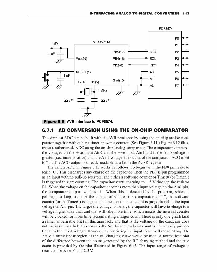
6.7.1 AD CONVERSION USING THE ON-CHIP COMPARATOR
The simplest ADC can be built with the AVR processor by using the on-chip analog com-parator together with either a timer or even a counter. (See Figure 6.11.) Figure 6.12 illus-trates a rather crude ADC using the on-chip analog comparator. The comparator comparesthe voltages on the �ve input Ain0 and the �ve input Ain1 and if the Ain0 voltage isgreater (i.e., more positive) than the Ain1 voltage, the output of the comparator ACO is setto “1”. The ACO output is directly readable as a bit in the ACSR register.
The simple ADC in Figure 6.12 works as follows. To begin with, the PB0 pin is set tologic “0”. This discharges any charge on the capacitor. Then the PB0 is pin programmedas an input with no pull-up resistors, and either a software counter or Timer0 (or Timer1)is triggered to start counting. The capacitor starts charging to �5 V through the resistorR1. When the voltage on the capacitor becomes more than input voltage on the Ain1 pin,the comparator output switches “1”. When this is detected by the program, which ispolling in a loop to detect the change of state of the comparator to “1”, the softwarecounter (or the Timer0) is stopped and the accumulated count is proportional to the inputvoltage on Ain-pin. The larger the voltage, on Ain-, the capacitor will have to charge to avoltage higher than that, and that will take more time, which means the internal counterwill be clocked for more time, accumulating a larger count. There is only one glitch (anda rather undesirable one) in this approach, and that is the voltage on the capacitor doesnot increase linearly but exponentially. So the accumulated count is not linearly propor-tional to the input voltage. However, by restricting the input to a small range of say 0 to2.5 V, a fairly linear region of the RC charging curve would be used. A normalized plotof the difference between the count generated by the RC charging method and the truecount is provided by the plot illustrated in Figure 6.13. The input range of voltage isrestricted between 0 and 2.5 V.
INTERFACING ANALOG-TO-DIGITAL CONVERTERS 113
Vcc(20)
RESET(1)
Gnd(10)
22 pF22 pF
4 MHz
.1 uF
+5V
.1 uF
X2(4) X1(5)
AT90S2313
PB5(17) SDA
PB4(16) SCL
INT*PD2(6)
P0
P1
P2
P3
P4
P5
P6
P7
PCF8574
A0
A1
A2
Figure 6.9 AVR interface to PCF8574.
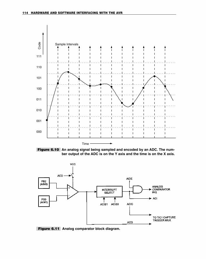
114 HARDWARE AND SOFTWARE INTERFACING WITH THE AVR
111
110
101
100
011
010
001
000
Sample Intervals
Time
Cod
e
Figure 6.10 An analog signal being sampled and encoded by an ADC. The num-ber output of the ADC is on the Y axis and the time is on the X axis.
Figure 6.11 Analog comparator block diagram.
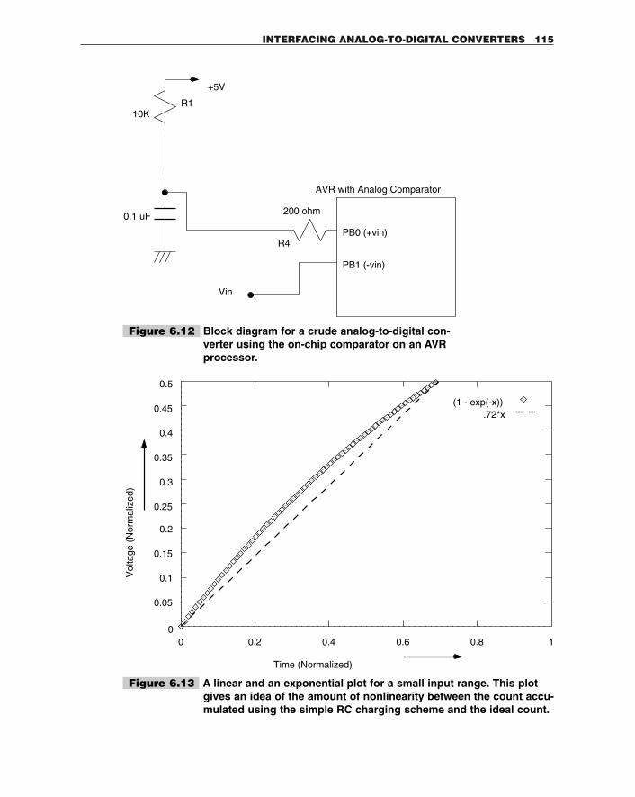
INTERFACING ANALOG-TO-DIGITAL CONVERTERS 115
10K
200 ohm
PB1 (-vin)
PB0 (+vin)
0.1 uF
R1
R4
+5V
AVR with Analog Comparator
Vin
Figure 6.12 Block diagram for a crude analog-to-digital con-verter using the on-chip comparator on an AVRprocessor.
0
0.05
0.1
0.15
0.2
0.25
0.3
0.35
0.4
0.45
0.5
0 0.2 0.4 0.6 0.8 1
(1 - exp(-x)).72*x
Vol
tage
(N
orm
aliz
ed)
Time (Normalized)
Figure 6.13 A linear and an exponential plot for a small input range. This plotgives an idea of the amount of nonlinearity between the count accu-mulated using the simple RC charging scheme and the ideal count.
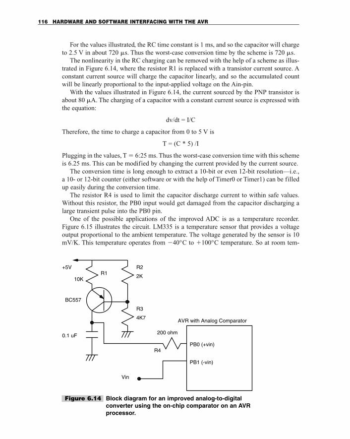
For the values illustrated, the RC time constant is 1 ms, and so the capacitor will chargeto 2.5 V in about 720 �s. Thus the worst-case conversion time by the scheme is 720 �s.
The nonlinearity in the RC charging can be removed with the help of a scheme as illus-trated in Figure 6.14, where the resistor R1 is replaced with a transistor current source. Aconstant current source will charge the capacitor linearly, and so the accumulated countwill be linearly proportional to the input-applied voltage on the Ain-pin.
With the values illustrated in Figure 6.14, the current sourced by the PNP transistor isabout 80 �A. The charging of a capacitor with a constant current source is expressed withthe equation:
dv/dt = I/C
Therefore, the time to charge a capacitor from 0 to 5 V is
T = (C * 5) /I
Plugging in the values, T � 6:25 ms. Thus the worst-case conversion time with this schemeis 6.25 ms. This can be modified by changing the current provided by the current source.
The conversion time is long enough to extract a 10-bit or even 12-bit resolution—i.e.,a 10- or 12-bit counter (either software or with the help of Timer0 or Timer1) can be filledup easily during the conversion time.
The resistor R4 is used to limit the capacitor discharge current to within safe values.Without this resistor, the PB0 input would get damaged from the capacitor discharging alarge transient pulse into the PB0 pin.
One of the possible applications of the improved ADC is as a temperature recorder.Figure 6.15 illustrates the circuit. LM335 is a temperature sensor that provides a voltageoutput proportional to the ambient temperature. The voltage generated by the sensor is 10mV/K. This temperature operates from �40°C to �100°C temperature. So at room tem-
116 HARDWARE AND SOFTWARE INTERFACING WITH THE AVR
+5V
BC557
2K
4K7
10K
200 ohm
PB1 (-vin)
PB0 (+vin)
0.1 uF
R1R2
R3
R4
AVR with Analog Comparator
Vin
Figure 6.14 Block diagram for an improved analog-to-digitalconverter using the on-chip comparator on an AVRprocessor.
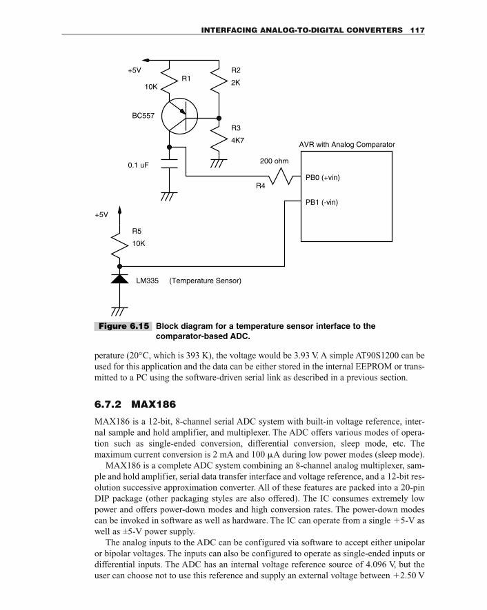
perature (20°C, which is 393 K), the voltage would be 3.93 V. A simple AT90S1200 can beused for this application and the data can be either stored in the internal EEPROM or trans-mitted to a PC using the software-driven serial link as described in a previous section.
6.7.2 MAX186
MAX186 is a 12-bit, 8-channel serial ADC system with built-in voltage reference, inter-nal sample and hold amplifier, and multiplexer. The ADC offers various modes of opera-tion such as single-ended conversion, differential conversion, sleep mode, etc. The maximum current conversion is 2 mA and 100 �A during low power modes (sleep mode).
MAX186 is a complete ADC system combining an 8-channel analog multiplexer, sam-ple and hold amplifier, serial data transfer interface and voltage reference, and a 12-bit res-olution successive approximation converter. All of these features are packed into a 20-pinDIP package (other packaging styles are also offered). The IC consumes extremely lowpower and offers power-down modes and high conversion rates. The power-down modescan be invoked in software as well as hardware. The IC can operate from a single �5-V aswell as ±5-V power supply.
The analog inputs to the ADC can be configured via software to accept either unipolaror bipolar voltages. The inputs can also be configured to operate as single-ended inputs ordifferential inputs. The ADC has an internal voltage reference source of 4.096 V, but theuser can choose not to use this reference and supply an external voltage between �2.50 V
INTERFACING ANALOG-TO-DIGITAL CONVERTERS 117
+5V
+5V
10K
LM335
BC557
2K
4K7
10K
200 ohm
(Temperature Sensor)
PB1 (-vin)
PB0 (+vin)
0.1 uF
R1R2
R3
R4
R5
AVR with Analog Comparator
Figure 6.15 Block diagram for a temperature sensor interface to thecomparator-based ADC.
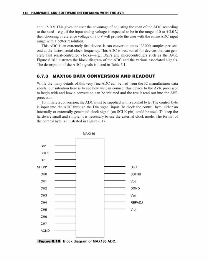
and �5.0 V. This gives the user the advantage of adjusting the span of the ADC accordingto the need—e.g., if the input analog voltage is expected to be in the range of 0 to �3.0 V,then choosing a reference voltage of 3.0 V will provide the user with the entire ADC inputrange with a better resolution.
This ADC is an extremely fast device. It can convert at up to 133000 samples per sec-ond at the fastest serial clock frequency. This ADC is best suited for devices that can gen-erate fast serial-controlled clocks—e.g., DSPs and microcontrollers such as the AVR.Figure 6.16 illustrates the block diagram of the ADC and the various associated signals.The description of the ADC signals is listed in Table 6.1.
6.7.3 MAX186 DATA CONVERSION AND READOUT
While the many details of this very fine ADC can be had from the IC manufacturer datasheets, our intention here is to see how we can connect this device to the AVR processorto begin with and how a conversion can be initiated and the result read out into the AVRprocessor.
To initiate a conversion, the ADC must be supplied with a control byte. The control byteis input into the ADC through the Din signal input. To clock the control byte, either aninternally or externally generated clock signal (on SCLK pin) could be used. To keep thehardware small and simple, it is necessary to use the external clock mode. The format ofthe control byte is illustrated in Figure 6.17.
118 HARDWARE AND SOFTWARE INTERFACING WITH THE AVR
CH7
CH6
CH5
CH4
CH3
CH2
CH1
CH0
AGND
SHDN*
Din
SCLK
CS*
Vref
REFADJ
Vss
DGND
Vdd
SSTRB
Dout
MAX186
Figure 6.16 Block diagram of MAX186 ADC.
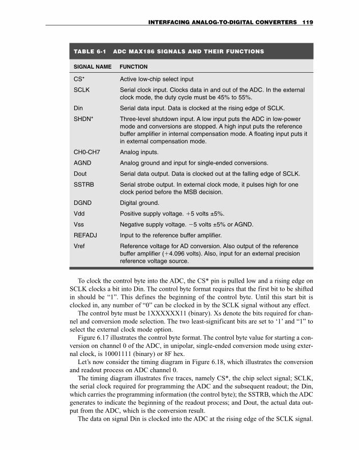
To clock the control byte into the ADC, the CS* pin is pulled low and a rising edge onSCLK clocks a bit into Din. The control byte format requires that the first bit to be shiftedin should be “1”. This defines the beginning of the control byte. Until this start bit isclocked in, any number of “0” can be clocked in by the SCLK signal without any effect.
The control byte must be 1XXXXXX11 (binary). Xs denote the bits required for chan-nel and conversion mode selection. The two least-significant bits are set to ‘1’ and “1” toselect the external clock mode option.
Figure 6.17 illustrates the control byte format. The control byte value for starting a con-version on channel 0 of the ADC, in unipolar, single-ended conversion mode using exter-nal clock, is 10001111 (binary) or 8F hex.
Let’s now consider the timing diagram in Figure 6.18, which illustrates the conversionand readout process on ADC channel 0.
The timing diagram illustrates five traces, namely CS*, the chip select signal; SCLK,the serial clock required for programming the ADC and the subsequent readout; the Din,which carries the programming information (the control byte); the SSTRB, which the ADCgenerates to indicate the beginning of the readout process; and Dout, the actual data out-put from the ADC, which is the conversion result.
The data on signal Din is clocked into the ADC at the rising edge of the SCLK signal.
INTERFACING ANALOG-TO-DIGITAL CONVERTERS 119
TABLE 6-1 ADC MAX186 SIGNALS AND THEIR FUNCTIONS
SIGNAL NAME FUNCTION
CS* Active low-chip select input
SCLK Serial clock input. Clocks data in and out of the ADC. In the externalclock mode, the duty cycle must be 45% to 55%.
Din Serial data input. Data is clocked at the rising edge of SCLK.
SHDN* Three-level shutdown input. A low input puts the ADC in low-powermode and conversions are stopped. A high input puts the referencebuffer amplifier in internal compensation mode. A floating input puts itin external compensation mode.
CH0-CH7 Analog inputs.
AGND Analog ground and input for single-ended conversions.
Dout Serial data output. Data is clocked out at the falling edge of SCLK.
SSTRB Serial strobe output. In external clock mode, it pulses high for oneclock period before the MSB decision.
DGND Digital ground.
Vdd Positive supply voltage. �5 volts ±5%.
Vss Negative supply voltage. �5 volts ±5% or AGND.
REFADJ Input to the reference buffer amplifier.
Vref Reference voltage for AD conversion. Also output of the referencebuffer amplifier (�4.096 volts). Also, input for an external precision reference voltage source.
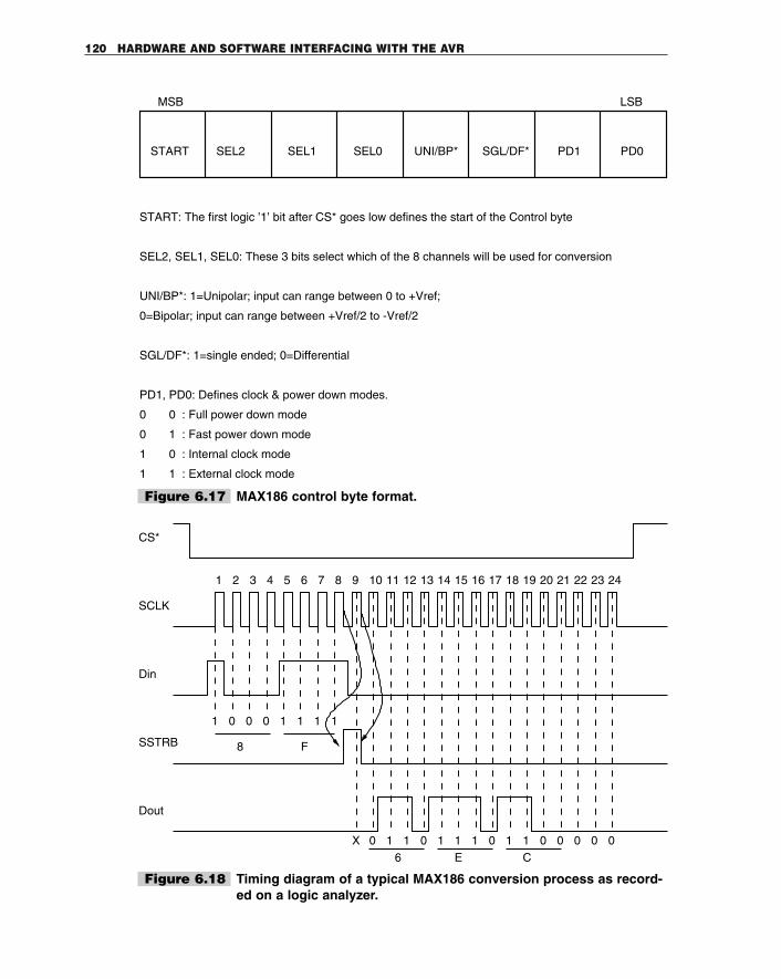
120 HARDWARE AND SOFTWARE INTERFACING WITH THE AVR
START: The first logic ’1’ bit after CS* goes low defines the start of the Control byte
1 1 : External clock mode
1 0 : Internal clock mode
0 1 : Fast power down mode
0 0 : Full power down mode
PD1, PD0: Defines clock & power down modes.
SGL/DF*: 1=single ended; 0=Differential
0=Bipolar; input can range between +Vref/2 to -Vref/2
UNI/BP*: 1=Unipolar; input can range between 0 to +Vref;
SEL2, SEL1, SEL0: These 3 bits select which of the 8 channels will be used for conversion
MSB LSB
PD0PD1SGL/DF*UNI/BP*SEL0SEL1SEL2START
Figure 6.17 MAX186 control byte format.
Dout
SSTRB
Din
SCLK
CS*
1 2 3 4 5 6 7 8 9 10 11 12 13 14 15 16 17 18 19 20 21 22 23 24
1 0 0 0 1 1 1 1
X 0 1 1 0 1 1 1 0 1 1 0 0 0 0 0
6 E C
8 F
Figure 6.18 Timing diagram of a typical MAX186 conversion process as record-ed on a logic analyzer.
The first bit that is clocked in is D7. To begin the conversion, D7 needs to be set to “1”, ascan also be seen from the value of the control byte that we calculated. So Din is set to “1”and the first SCLK rising edge is applied to the ADC. The SCLK is then taken low.
Thereafter, the Din is set to each of the subsequent bits of the control byte before apply-ing the SCLK. At the end of 8 SCLK pulses, the Din bit is not required and is set to “0”.At the falling edge of the 8th SCLK pulse, the ADC sets the SSTRB bit to “1”. At thefalling edge of the 9th SCLK bit, SSTRB is taken to “0”.
At the falling edge of the 9th SCLK signal, the ADC outputs data on the Dout signal,one bit for each of the next 15 falling edges of the SCLK signal. The data on the 9th pulseis “0” and the actual conversion result is effective after the 10th falling edge to the 21st ris-ing edge. Thereafter, for the next 3 edges, the ADC outputs “0”s.
For a controller circuit such as the AVR, with minimal parts, to initiate conversion andreadout the result would need three output bits and one input bit. The output bits would beneeded to generate the Din and SCLK signal and the input bit to read the Dout signal fromthe ADC.
Figure 6.19 illustrates the circuit with a MAX186 ADC, an AT90S2313 processor, anda MAX232 RS-232 level translator. The circuit is connected to the PC serial port. The AVRprocessor waits for a command from the PC and then initiates conversion on the MAX186and sends out the data back to the PC serial port.
The program is available on the CD. The code for this project is available in the codedirectory in the file MX186_ex.asm.
6.7.4 MAX110/MAX111
MAX111/MAX110 is a serial 14-bit, dual-channel ADC from Maxim. MAX111-/MAX110 ADC uses an internal autocalibration technique to achieve 14-bit resolutionwithout any external component. The ADC offers two channels of ADC conversion andoperates with 650�A current, thus making it ideal for portable, battery-operated dataacquisition operations.
MAX111 operates from a single �5-V power supply and converts differential signalsin the range of ±1.5 V or differential signals in the range of 0 to 1.5 V.
MAX111 can operate from an external as well as internal oversampling clock that isused for the ADC conversion. To start a conversion, digital data is shifted into theMAX111 serial register after pulling the CS low. CS can only be pulled low when BUSYis inactive. MAX111 has a fully static serial I/O shift register which can be read at any ser-ial clock (SCLK) rates from DC to 2 MHz. Input data to the ADC is clocked in at the ris-ing edge of the SCLK and the output data from the ADC (conversion result) is clocked outat SCLK falling edge and should be read on SCLK rising edge.
The data clocked into the ADC determines the ADC operation, which could be to initi-ate a new conversion, calibrate the ADC, perform offset null, change ADC channel, changeoversampling clock divider ratio, etc.
The format of this control word is as follows:
bit # 15 14 13 12 11 10 9 8No-op NU NU CONV4 CONV3 CONV2 CONV1 DV4
bit # 7 6 5 4 3 2 1 0DV2 NU NU CHS CAL NUL PDX PD
INTERFACING ANALOG-TO-DIGITAL CONVERTERS 121
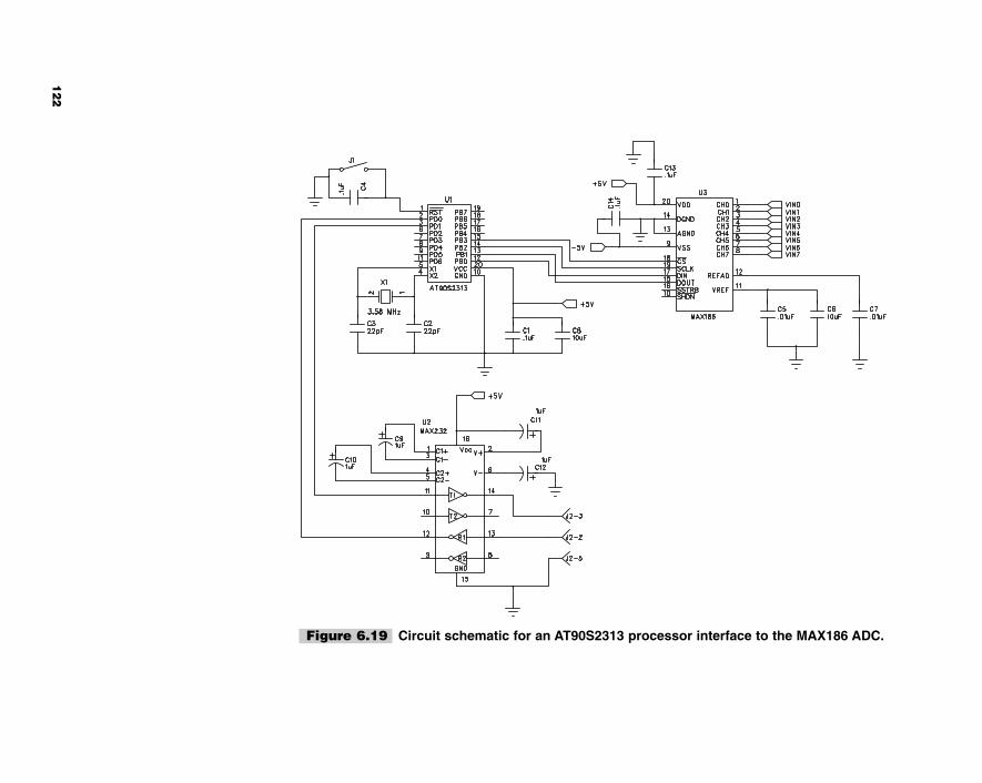
Figure 6.19 Circuit schematic for an AT90S2313 processor interface to the MAX186 ADC.
122
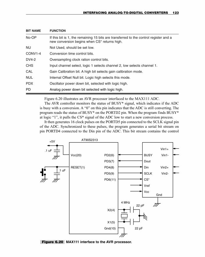
BIT NAME FUNCTION
No-OP If this bit is 1, the remaining 15 bits are transferred to the control register and anew conversion begins when CS* returns high.
NU Not Used, should be set low.
CONV1-4 Conversion time control bits.
DV4-2 Oversampling clock ration control bits.
CHS Input channel select, logic 1 selects channel 2, low selects channel 1.
CAL Gain Calibration bit. A high bit selects gain calibration mode.
NUL Internal Offset Null bit. Logic high selects this mode.
PDX Oscillator power down bit, selected with logic high.
PD Analog power down bit selected with logic high.
Figure 6.20 illustrates an AVR processor interfaced to the MAX111 ADC.The AVR controller monitors the status of BUSY* signal, which indicates if the ADC
is busy with a conversion. A “0” on this pin indicates that the ADC is still converting. Theprogram reads the status of BUSY* on the PORTD2 pin. When the program finds BUSY*at logic “1”, it pulls the CS* signal of the ADC low to start a new conversion process.
It then generates 16 clock pulses on the PORTD5 pin connected to the SCLK signal pinof the ADC. Synchronized to these pulses, the program generates a serial bit stream on pin PORTD4 connected to the Din pin of the ADC. This bit stream contains the control
INTERFACING ANALOG-TO-DIGITAL CONVERTERS 123
Vcc(20)
RESET(1).1 uF
+5V
.1 uF
Gnd(10)
22 pF4 MHz
22 pF
X2(4)
X1(5)
AT90S2313
PD2(6)
PD3(7)
PD4(8)
PD5(9)
PD6(11)
BUSY
Dout
Din
SCLK
CS*
Vref
Vin1+
Vin1-
Vin2+
Vin2-
VccGnd
Figure 6.20 MAX111 interface to the AVR processor.
word with the format described previously. Output data from the ADC is clocked out onDout pin on the falling edges of the SCLK pulses. The program reads this data on thePORTD3 pin. The CS* signal connected to the PORTD6 pin is pulled up after the 16 clockpulses are generated.
The ADC pulls its BUSY* signal low while the conversion is in progress. The conver-sion time depends upon the XCLK frequency and the format of the control word. In thiscircuit, the internal RC oscillator is used for the conversion clock. The converted data isclocked out in the next round of the clocking sequence by the ADC.
Figure 6.21 illustrates the timing diagram of a typical conversion and readout sequencerecorded on a logic analyzer. A suitable data conversion and readout driver code is includ-ed in a later project chapter. The driver program is in “C”.
6.8 Interfacing Digital-to-AnalogConvertersDigital-to-Analog Converters (DACs) are devices that function exactly opposite to theADCs. DACs convert digital data to analog voltage (or current). Functionally, the DAC hasn digital input lines and 1 output line that provides analog voltage or current. The analogoutput is proportional to the weighted sum of the digital inputs.
6.8.1 USING PWM FOR A DAC
Pulse Width Modulation (PWM) technique can be used easily to create a DAC, especiallysince many of the members of the AVR processor family are equipped with on-chip PWM.
In PWM, a digital signal of fixed frequency is generated. The pulse width of the signalis changed according to the requirement. Ideally, it should be possible to vary the width toany arbitrary value. However, with a counter-based PWM, the change can be only as muchas the resolution of the counter. A PWM implemented using an 8-bit counter can onlychange the pulse width by 0.4% approximately (1 bit in 255). By employing a low-pass fil-ter at the output of a PWM wave, the average value of the signal is extracted. The averagevalue of a digital signal is equal to the duty cycle of the waveform.
Figure 6.22 illustrates a 2-bit PWM signal. Figure 6.23 illustrates a DAC using thebuilt-in PWM generator on output PORTB3 pin and an external RC filter. The RC filterhas a bandwidth of about 16 Hz for the values illustrated. The Timer1 can be clocked atthe system clock frequency of 4 MHz as illustrated, and for an 8-bit PWM, the PWM fre-quency will be about 7800 Hz. The RC filter will cleanly filter out the high-frequencycomponents, and a clean DC value will be produced.
6.8.2 R-2R LADDER DAC
Using only two different values of resistors, it is possible to build a simple R-2R ladderDAC of reasonable linearity. Figure 6.24 illustrates a R-2R ladder DAC connected to thePORTB of the AT90S1200. To use the DAC, the following code can be used.
124 HARDWARE AND SOFTWARE INTERFACING WITH THE AVR
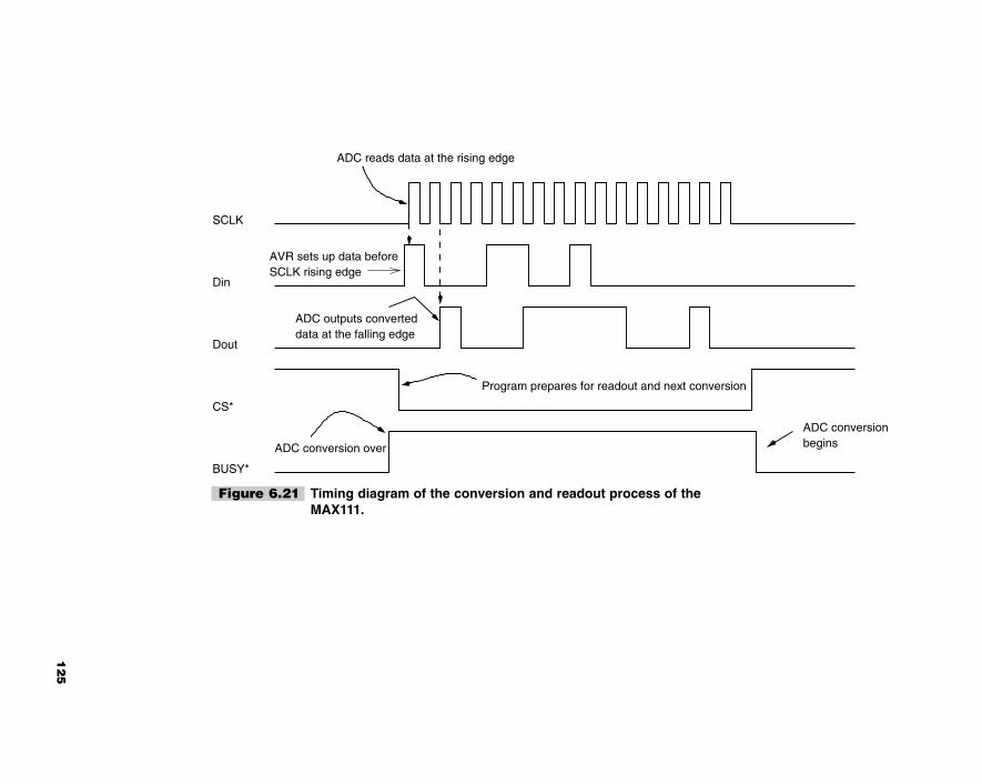
SCLK
Din
Dout
CS*
BUSY*
ADC conversion over
Program prepares for readout and next conversion
ADC conversionbegins
data at the falling edgeADC outputs converted
ADC reads data at the rising edge
SCLK rising edgeAVR sets up data before
12
5
Figure 6.21 Timing diagram of the conversion and readout process of theMAX111.
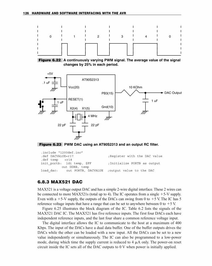
.include “1200def.inc”
.def DACVALUE=r17 ;Register with the DAC value
.def temp =r18init_portb: ldi temp, $FF ;Initialize PORTB as output
out DDRB, tempload_dac: out PORTB, DACVALUE ;output value to the DAC
6.8.3 MAX521 DAC
MAX521 is a voltage output DAC and has a simple 2-wire digital interface. These 2 wires canbe connected to more MAX521s (total up to 4). The IC operates from a single �5-V supply.Even with a �5-V supply, the outputs of the DACs can swing from 0 to �5 V. The IC has 5reference voltage inputs that have a range that can be set to anywhere between 0 to �5 V.
Figure 6.25 illustrates the block diagram of the IC. Table 6.2 lists the signals of theMAX521 DAC IC. The MAX521 has five reference inputs. The first four DACs each haveindependent reference inputs, and the last four share a common reference voltage input.
The digital interface allows the IC to communicate to the host at a maximum of 400Kbps. The input of the DACs have a dual data buffer. One of the buffer outputs drives theDACs while the other can be loaded with a new input. All the DACs can be set to a newvalue independently or simultaneously. The IC can also be programmed to a low-powermode, during which time the supply current is reduced to 4 �A only. The power-on resetcircuit inside the IC sets all of the DAC outputs to 0 V when power is initially applied.
126 HARDWARE AND SOFTWARE INTERFACING WITH THE AVR
2 3 4 00 1
Vcc(20)
RESET(1)
Gnd(10)
22 pF22 pF
4 MHz
.1 uF
+5V
.1 uF
X2(4) X1(5)
AT90S2313
PB3(15)
10 KOhm
1 uF
DAC Output
Figure 6.22 A continuously varying PWM signal. The average value of the signalchanges by 25% in each period.
Figure 6.23 PWM DAC using an AT90S2313 and an output RC filter.
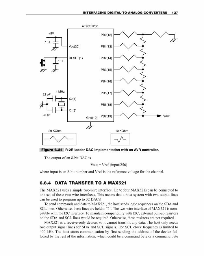
The output of an 8-bit DAC is
Vout = Vref (input/256)
where input is an 8-bit number and Vref is the reference voltage for the channel.
6.8.4 DATA TRANSFER TO A MAX521
The MAX521 uses a simple two-wire interface. Up to four MAX521s can be connected toone set of these two-wire interfaces. This means that a host system with two output linescan be used to program up to 32 DACs!
To send commands and data to MAX521, the host sends logic sequences on the SDA andSCL lines. Otherwise, these lines are held to “1”. The two-wire interface of MAX521 is com-patible with the I2C interface. To maintain compatibility with I2C, external pull-up resistorson the SDA and SCL lines would be required. Otherwise, these resistors are not required.
MAX521 is a receive-only device, so it cannot transmit any data. The host only needstwo output signal lines for SDA and SCL signals. The SCL clock frequency is limited to400 kHz. The host starts communication by first sending the address of the device fol-lowed by the rest of the information, which could be a command byte or a command byte
INTERFACING DIGITAL-TO-ANALOG CONVERTERS 127
Vcc(20)
RESET(1).1 uF
+5V
.1 uF
X2(4)
X1(5)
4 MHz22 pF
22 pFGnd(10)
AT90S1200
PB0(12)
PB1(13)
PB2(14)
PB3(15)
PB4(16)
PB5(17)
PB6(18)
PB7(19) Vout
20 KOhm 10 KOhm
Figure 6.24 R-2R ladder DAC implementation with an AVR controller.
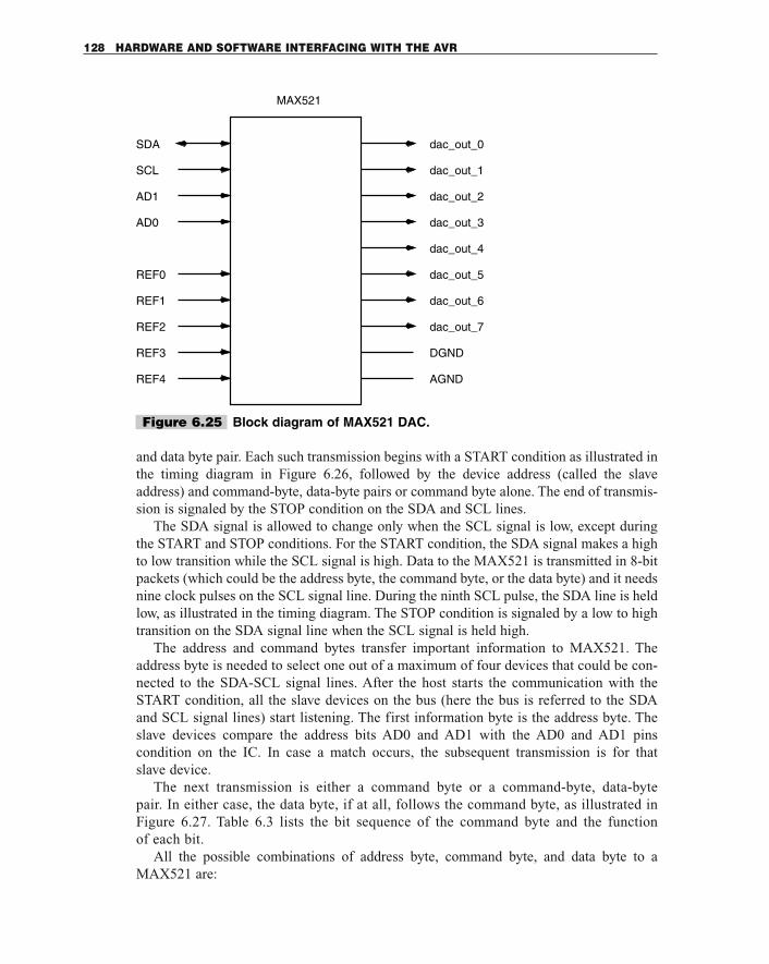
and data byte pair. Each such transmission begins with a START condition as illustrated inthe timing diagram in Figure 6.26, followed by the device address (called the slaveaddress) and command-byte, data-byte pairs or command byte alone. The end of transmis-sion is signaled by the STOP condition on the SDA and SCL lines.
The SDA signal is allowed to change only when the SCL signal is low, except duringthe START and STOP conditions. For the START condition, the SDA signal makes a highto low transition while the SCL signal is high. Data to the MAX521 is transmitted in 8-bitpackets (which could be the address byte, the command byte, or the data byte) and it needsnine clock pulses on the SCL signal line. During the ninth SCL pulse, the SDA line is heldlow, as illustrated in the timing diagram. The STOP condition is signaled by a low to hightransition on the SDA signal line when the SCL signal is held high.
The address and command bytes transfer important information to MAX521. Theaddress byte is needed to select one out of a maximum of four devices that could be con-nected to the SDA-SCL signal lines. After the host starts the communication with theSTART condition, all the slave devices on the bus (here the bus is referred to the SDAand SCL signal lines) start listening. The first information byte is the address byte. Theslave devices compare the address bits AD0 and AD1 with the AD0 and AD1 pins condition on the IC. In case a match occurs, the subsequent transmission is for that slave device.
The next transmission is either a command byte or a command-byte, data-byte pair. In either case, the data byte, if at all, follows the command byte, as illustrated inFigure 6.27. Table 6.3 lists the bit sequence of the command byte and the function of each bit.
All the possible combinations of address byte, command byte, and data byte to aMAX521 are:
128 HARDWARE AND SOFTWARE INTERFACING WITH THE AVR
REF4
REF3
REF2
REF1
REF0
AD0
AD1
SCL
SDA
AGND
DGND
dac_out_7
dac_out_6
dac_out_5
dac_out_4
dac_out_3
dac_out_2
dac_out_1
dac_out_0
MAX521
Figure 6.25 Block diagram of MAX521 DAC.
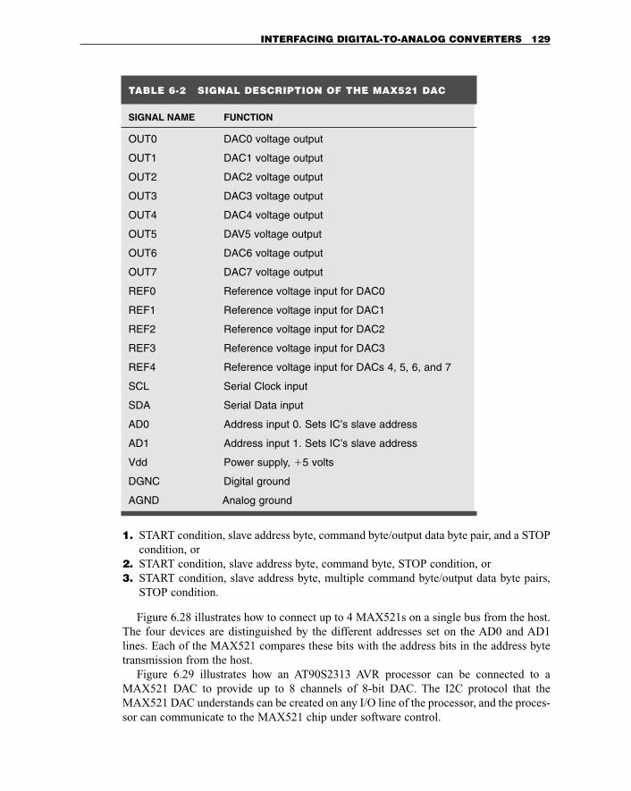
1. START condition, slave address byte, command byte/output data byte pair, and a STOPcondition, or
2. START condition, slave address byte, command byte, STOP condition, or3. START condition, slave address byte, multiple command byte/output data byte pairs,
STOP condition.
Figure 6.28 illustrates how to connect up to 4 MAX521s on a single bus from the host.The four devices are distinguished by the different addresses set on the AD0 and AD1lines. Each of the MAX521 compares these bits with the address bits in the address bytetransmission from the host.
Figure 6.29 illustrates how an AT90S2313 AVR processor can be connected to aMAX521 DAC to provide up to 8 channels of 8-bit DAC. The I2C protocol that theMAX521 DAC understands can be created on any I/O line of the processor, and the proces-sor can communicate to the MAX521 chip under software control.
INTERFACING DIGITAL-TO-ANALOG CONVERTERS 129
TABLE 6-2 SIGNAL DESCRIPTION OF THE MAX521 DAC
SIGNAL NAME FUNCTION
OUT0 DAC0 voltage output
OUT1 DAC1 voltage output
OUT2 DAC2 voltage output
OUT3 DAC3 voltage output
OUT4 DAC4 voltage output
OUT5 DAV5 voltage output
OUT6 DAC6 voltage output
OUT7 DAC7 voltage output
REF0 Reference voltage input for DAC0
REF1 Reference voltage input for DAC1
REF2 Reference voltage input for DAC2
REF3 Reference voltage input for DAC3
REF4 Reference voltage input for DACs 4, 5, 6, and 7
SCL Serial Clock input
SDA Serial Data input
AD0 Address input 0. Sets IC’s slave address
AD1 Address input 1. Sets IC’s slave address
Vdd Power supply, �5 volts
DGNC Digital ground
AGND Analog ground
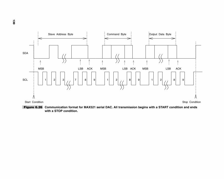
Start Condition Stop Condition
SCL
SDA
Slave Address Byte Command Byte Output Data Byte
LSB ACKMSBACKLSBMSBACKLSBMSB
1 2 3 7 8 9 1 2 8 9 1 2 8 9
Figure 6.26 Communication format for MAX521 serial DAC. All transmission begins with a START condition and endswith a STOP condition.
130
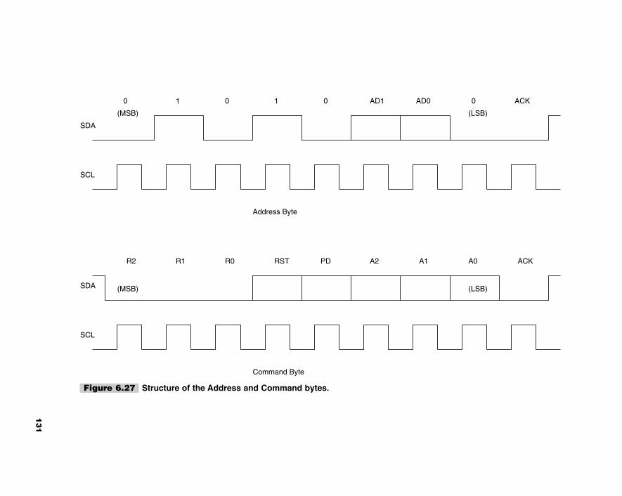
Command Byte
(MSB) (LSB)
ACKA0A1A2PDRSTR0R1R2
(MSB) (LSB)
Address Byte
SDA
SCL
0 1 0 1 0 AD1 AD0 0 ACK
SCL
SDA
Figure 6.27 Structure of the Address and Command bytes.
13
1
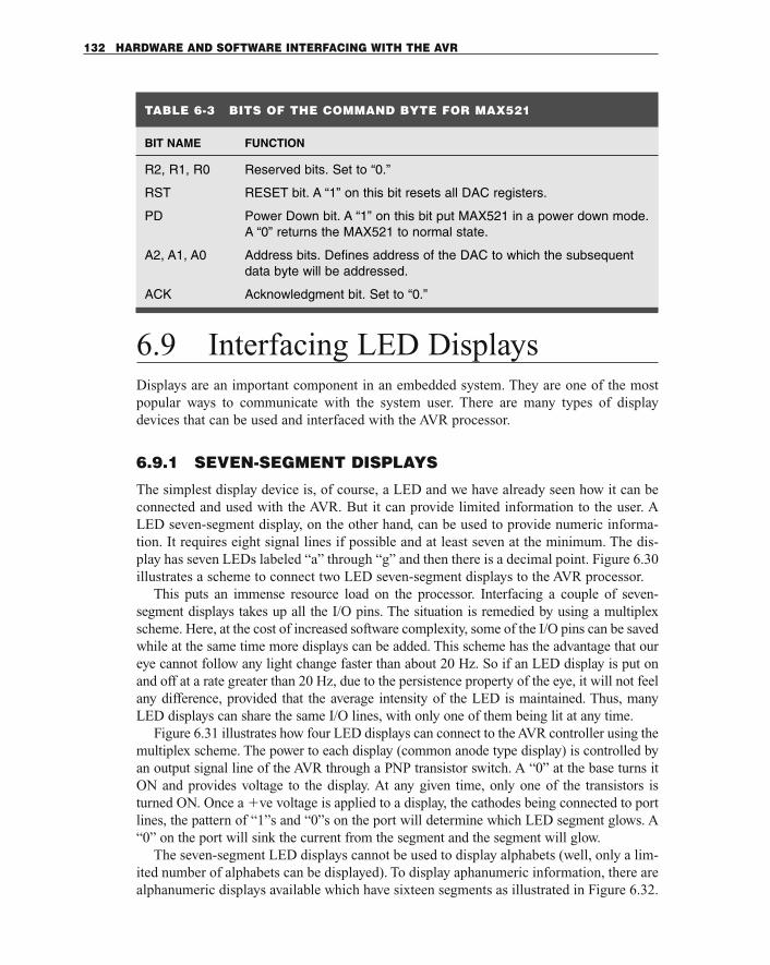
6.9 Interfacing LED DisplaysDisplays are an important component in an embedded system. They are one of the mostpopular ways to communicate with the system user. There are many types of displaydevices that can be used and interfaced with the AVR processor.
6.9.1 SEVEN-SEGMENT DISPLAYS
The simplest display device is, of course, a LED and we have already seen how it can beconnected and used with the AVR. But it can provide limited information to the user. ALED seven-segment display, on the other hand, can be used to provide numeric informa-tion. It requires eight signal lines if possible and at least seven at the minimum. The dis-play has seven LEDs labeled “a” through “g” and then there is a decimal point. Figure 6.30illustrates a scheme to connect two LED seven-segment displays to the AVR processor.
This puts an immense resource load on the processor. Interfacing a couple of seven-segment displays takes up all the I/O pins. The situation is remedied by using a multiplexscheme. Here, at the cost of increased software complexity, some of the I/O pins can be savedwhile at the same time more displays can be added. This scheme has the advantage that oureye cannot follow any light change faster than about 20 Hz. So if an LED display is put onand off at a rate greater than 20 Hz, due to the persistence property of the eye, it will not feelany difference, provided that the average intensity of the LED is maintained. Thus, manyLED displays can share the same I/O lines, with only one of them being lit at any time.
Figure 6.31 illustrates how four LED displays can connect to the AVR controller using themultiplex scheme. The power to each display (common anode type display) is controlled byan output signal line of the AVR through a PNP transistor switch. A “0” at the base turns itON and provides voltage to the display. At any given time, only one of the transistors isturned ON. Once a �ve voltage is applied to a display, the cathodes being connected to portlines, the pattern of “1”s and “0”s on the port will determine which LED segment glows. A“0” on the port will sink the current from the segment and the segment will glow.
The seven-segment LED displays cannot be used to display alphabets (well, only a lim-ited number of alphabets can be displayed). To display aphanumeric information, there arealphanumeric displays available which have sixteen segments as illustrated in Figure 6.32.
132 HARDWARE AND SOFTWARE INTERFACING WITH THE AVR
TABLE 6-3 BITS OF THE COMMAND BYTE FOR MAX521
BIT NAME FUNCTION
R2, R1, R0 Reserved bits. Set to “0.”
RST RESET bit. A “1” on this bit resets all DAC registers.
PD Power Down bit. A “1” on this bit put MAX521 in a power down mode.A “0” returns the MAX521 to normal state.
A2, A1, A0 Address bits. Defines address of the DAC to which the subsequentdata byte will be addressed.
ACK Acknowledgment bit. Set to “0.”
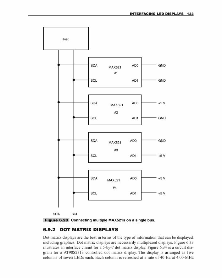
6.9.2 DOT MATRIX DISPLAYS
Dot matrix displays are the best in terms of the type of information that can be displayed,including graphics. Dot matrix displays are necessarily multiplexed displays. Figure 6.33illustrates an interface circuit for a 5-by-7 dot matrix display. Figure 6.34 is a circuit dia-gram for a AT90S2313 controlled dot matrix display. The display is arranged as fivecolumns of seven LEDs each. Each column is refreshed at a rate of 40 Hz at 4.00-MHz
INTERFACING LED DISPLAYS 133
+5 V
+5 V
+5 V
GND
GND
+5 V
GND
GND
AD1
AD0
AD1
AD0
AD1
AD0
AD1
AD0
SCL
SDA
SCL
SDA
SCL
SDA
SCL
SDA
#4
MAX521
#3
MAX521
#2
MAX521
#1
MAX521
SCLSDA
Host
Figure 6.28 Connecting multiple MAX521s on a single bus.
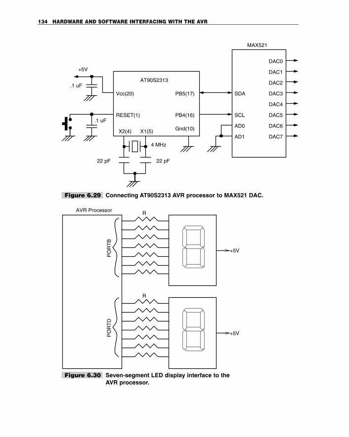
134 HARDWARE AND SOFTWARE INTERFACING WITH THE AVR
Vcc(20)
RESET(1)
Gnd(10)
22 pF22 pF
4 MHz
.1 uF
+5V
.1 uF
X2(4) X1(5)
AT90S2313
MAX521
PB5(17)
PB4(16)
SDA
SCL
AD0
AD1
DAC0
DAC1
DAC2
DAC3
DAC4
DAC5
DAC6
DAC7
Figure 6.29 Connecting AT90S2313 AVR processor to MAX521 DAC.
+5V
R
+5V
R
AVR Processor
PO
RT
BP
OR
TD
Figure 6.30 Seven-segment LED display interface to theAVR processor.
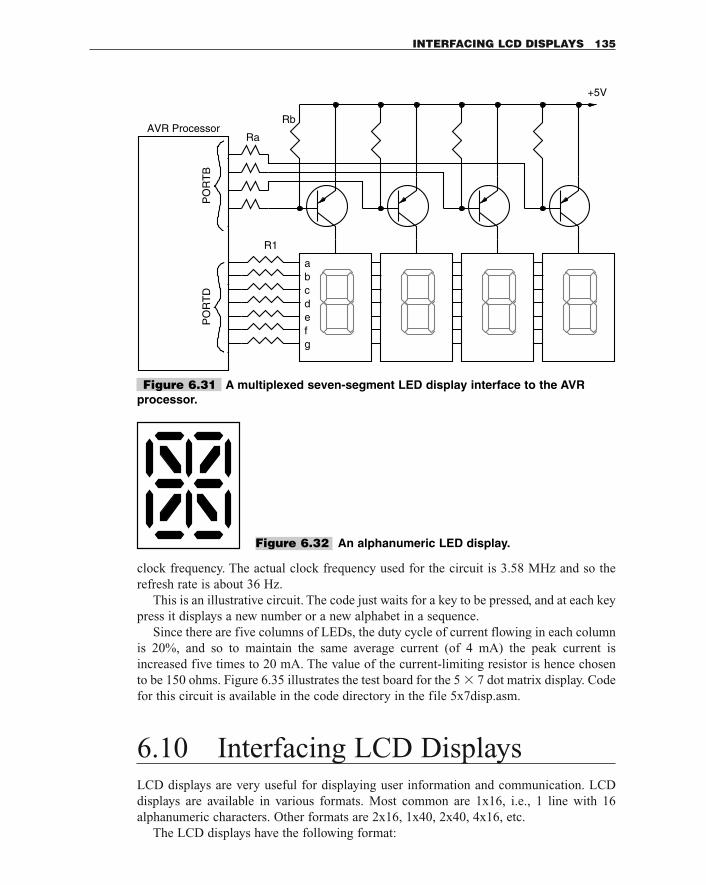
clock frequency. The actual clock frequency used for the circuit is 3.58 MHz and so therefresh rate is about 36 Hz.
This is an illustrative circuit. The code just waits for a key to be pressed, and at each keypress it displays a new number or a new alphabet in a sequence.
Since there are five columns of LEDs, the duty cycle of current flowing in each columnis 20%, and so to maintain the same average current (of 4 mA) the peak current isincreased five times to 20 mA. The value of the current-limiting resistor is hence chosento be 150 ohms. Figure 6.35 illustrates the test board for the 5 � 7 dot matrix display. Codefor this circuit is available in the code directory in the file 5x7disp.asm.
6.10 Interfacing LCD DisplaysLCD displays are very useful for displaying user information and communication. LCDdisplays are available in various formats. Most common are 1x16, i.e., 1 line with 16alphanumeric characters. Other formats are 2x16, 1x40, 2x40, 4x16, etc.
The LCD displays have the following format:
INTERFACING LCD DISPLAYS 135
AVR Processor
PO
RT
DP
OR
TB
+5V
R1
Ra
Rb
abcdefg
Figure 6.31 A multiplexed seven-segment LED display interface to the AVRprocessor.
Figure 6.32 An alphanumeric LED display.
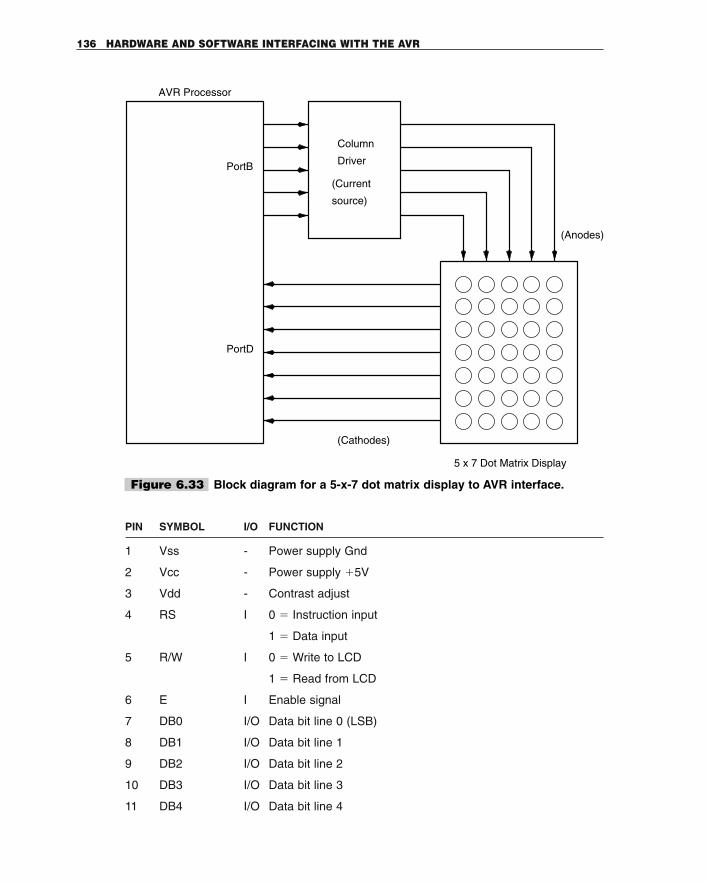
PIN SYMBOL I/O FUNCTION
1 Vss - Power supply Gnd
2 Vcc - Power supply �5V
3 Vdd - Contrast adjust
4 RS I 0 � Instruction input
1 � Data input
5 R/W I 0 � Write to LCD
1 � Read from LCD
6 E I Enable signal
7 DB0 I/O Data bit line 0 (LSB)
8 DB1 I/O Data bit line 1
9 DB2 I/O Data bit line 2
10 DB3 I/O Data bit line 3
11 DB4 I/O Data bit line 4
136 HARDWARE AND SOFTWARE INTERFACING WITH THE AVR
Column
Driver
(Current
source)
5 x 7 Dot Matrix Display
(Anodes)
(Cathodes)
AVR Processor
PortB
PortD
Figure 6.33 Block diagram for a 5-x-7 dot matrix display to AVR interface.
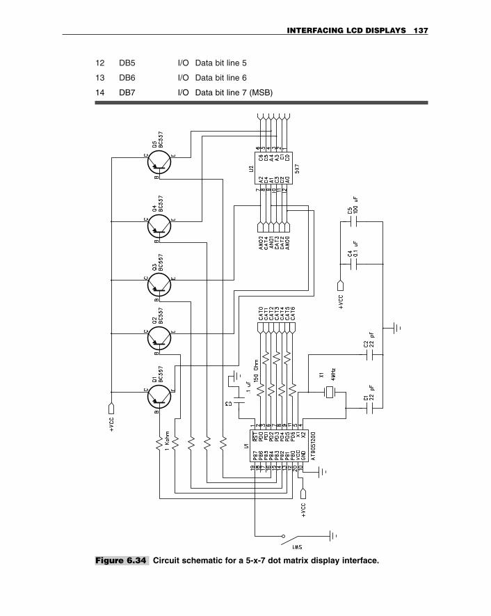
12 DB5 I/O Data bit line 5
13 DB6 I/O Data bit line 6
14 DB7 I/O Data bit line 7 (MSB)
INTERFACING LCD DISPLAYS 137
Figure 6.34 Circuit schematic for a 5-x-7 dot matrix display interface.
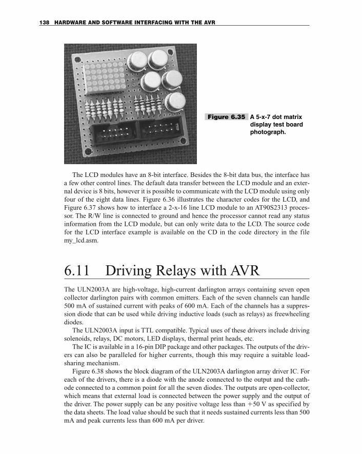
The LCD modules have an 8-bit interface. Besides the 8-bit data bus, the interface hasa few other control lines. The default data transfer between the LCD module and an exter-nal device is 8 bits, however it is possible to communicate with the LCD module using onlyfour of the eight data lines. Figure 6.36 illustrates the character codes for the LCD, andFigure 6.37 shows how to interface a 2-x-16 line LCD module to an AT90S2313 proces-sor. The R/W line is connected to ground and hence the processor cannot read any statusinformation from the LCD module, but can only write data to the LCD. The source codefor the LCD interface example is available on the CD in the code directory in the filemy_lcd.asm.
6.11 Driving Relays with AVRThe ULN2003A are high-voltage, high-current darlington arrays containing seven opencollector darlington pairs with common emitters. Each of the seven channels can handle500 mA of sustained current with peaks of 600 mA. Each of the channels has a suppres-sion diode that can be used while driving inductive loads (such as relays) as freewheelingdiodes.
The ULN2003A input is TTL compatible. Typical uses of these drivers include drivingsolenoids, relays, DC motors, LED displays, thermal print heads, etc.
The IC is available in a 16-pin DIP package and other packages. The outputs of the driv-ers can also be paralleled for higher currents, though this may require a suitable load-sharing mechanism.
Figure 6.38 shows the block diagram of the ULN2003A darlington array driver IC. Foreach of the drivers, there is a diode with the anode connected to the output and the cath-ode connected to a common point for all the seven diodes. The outputs are open-collector,which means that external load is connected between the power supply and the output ofthe driver. The power supply can be any positive voltage less than �50 V as specified bythe data sheets. The load value should be such that it needs sustained currents less than 500mA and peak currents less than 600 mA per driver.
138 HARDWARE AND SOFTWARE INTERFACING WITH THE AVR
Figure 6.35 A 5-x-7 dot matrixdisplay test boardphotograph.
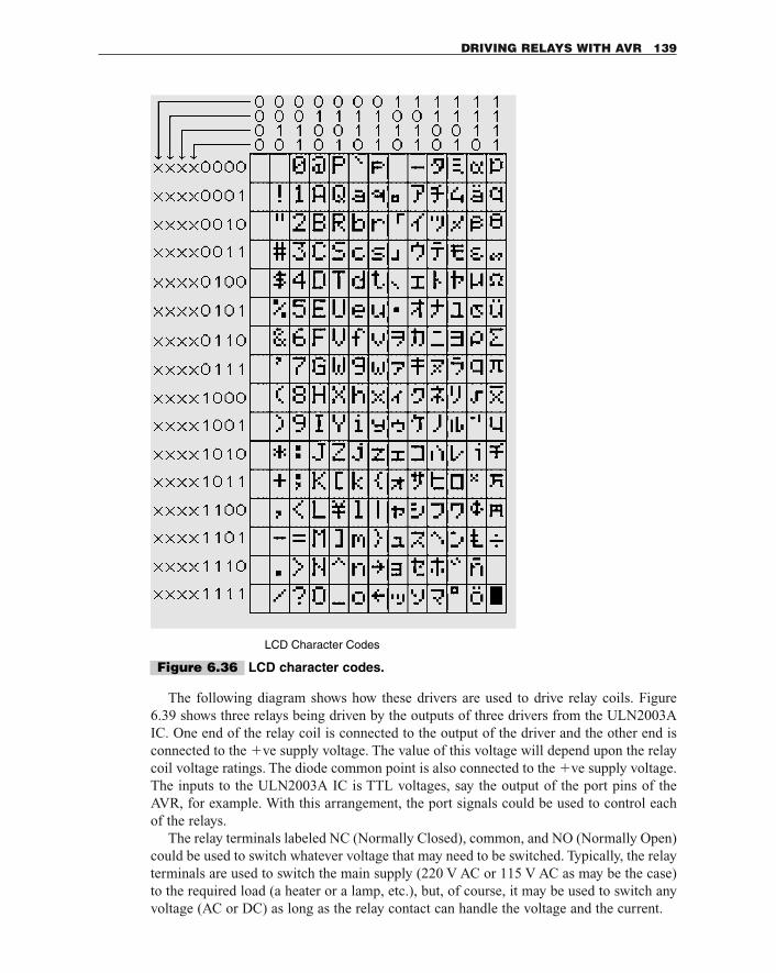
The following diagram shows how these drivers are used to drive relay coils. Figure6.39 shows three relays being driven by the outputs of three drivers from the ULN2003AIC. One end of the relay coil is connected to the output of the driver and the other end isconnected to the �ve supply voltage. The value of this voltage will depend upon the relaycoil voltage ratings. The diode common point is also connected to the �ve supply voltage.The inputs to the ULN2003A IC is TTL voltages, say the output of the port pins of theAVR, for example. With this arrangement, the port signals could be used to control eachof the relays.
The relay terminals labeled NC (Normally Closed), common, and NO (Normally Open)could be used to switch whatever voltage that may need to be switched. Typically, the relayterminals are used to switch the main supply (220 V AC or 115 V AC as may be the case)to the required load (a heater or a lamp, etc.), but, of course, it may be used to switch anyvoltage (AC or DC) as long as the relay contact can handle the voltage and the current.
DRIVING RELAYS WITH AVR 139
LCD Character Codes
Figure 6.36 LCD character codes.
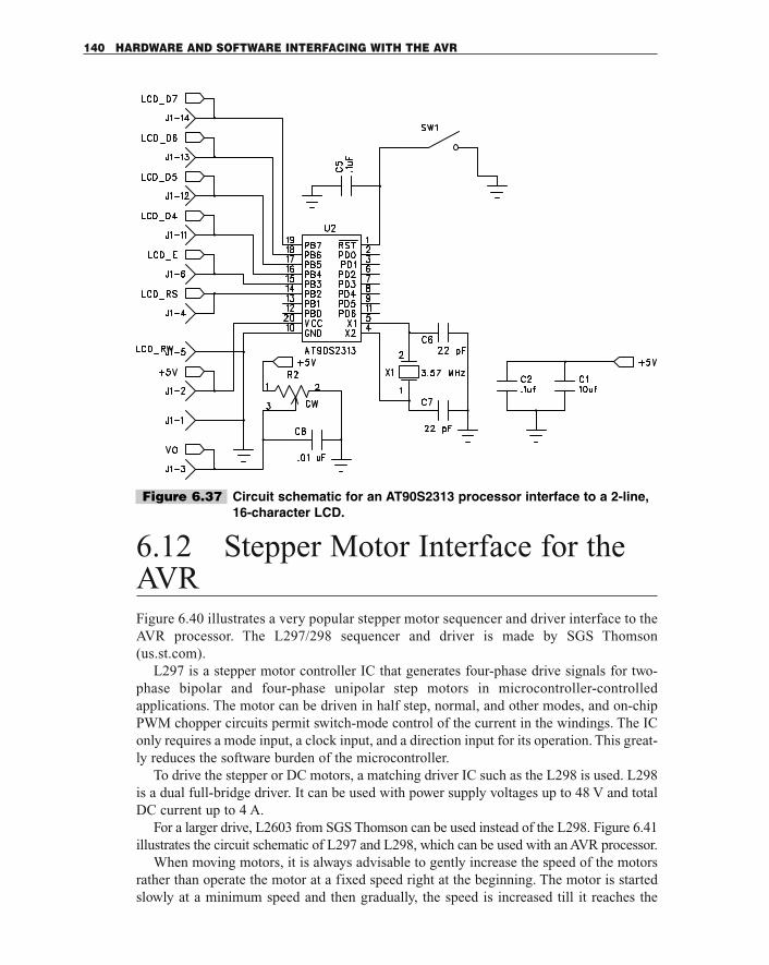
6.12 Stepper Motor Interface for theAVRFigure 6.40 illustrates a very popular stepper motor sequencer and driver interface to theAVR processor. The L297/298 sequencer and driver is made by SGS Thomson(us.st.com).
L297 is a stepper motor controller IC that generates four-phase drive signals for two-phase bipolar and four-phase unipolar step motors in microcontroller-controlled applications. The motor can be driven in half step, normal, and other modes, and on-chipPWM chopper circuits permit switch-mode control of the current in the windings. The IConly requires a mode input, a clock input, and a direction input for its operation. This great-ly reduces the software burden of the microcontroller.
To drive the stepper or DC motors, a matching driver IC such as the L298 is used. L298is a dual full-bridge driver. It can be used with power supply voltages up to 48 V and totalDC current up to 4 A.
For a larger drive, L2603 from SGS Thomson can be used instead of the L298. Figure 6.41illustrates the circuit schematic of L297 and L298, which can be used with an AVR processor.
When moving motors, it is always advisable to gently increase the speed of the motorsrather than operate the motor at a fixed speed right at the beginning. The motor is startedslowly at a minimum speed and then gradually, the speed is increased till it reaches the
140 HARDWARE AND SOFTWARE INTERFACING WITH THE AVR
Figure 6.37 Circuit schematic for an AT90S2313 processor interface to a 2-line,16-character LCD.
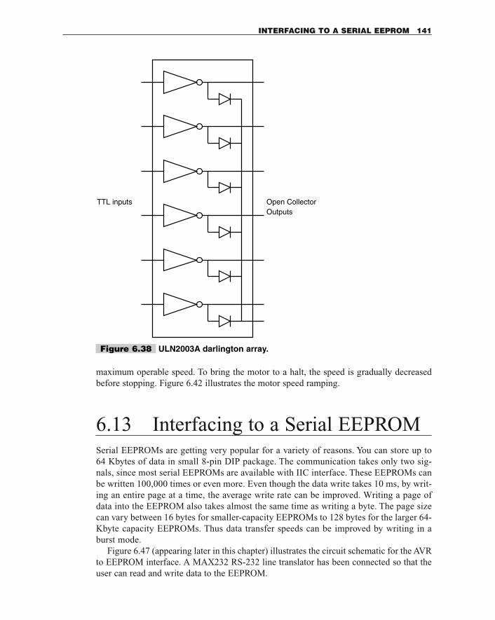
maximum operable speed. To bring the motor to a halt, the speed is gradually decreasedbefore stopping. Figure 6.42 illustrates the motor speed ramping.
6.13 Interfacing to a Serial EEPROMSerial EEPROMs are getting very popular for a variety of reasons. You can store up to64 Kbytes of data in small 8-pin DIP package. The communication takes only two sig-nals, since most serial EEPROMs are available with IIC interface. These EEPROMs canbe written 100,000 times or even more. Even though the data write takes 10 ms, by writ-ing an entire page at a time, the average write rate can be improved. Writing a page ofdata into the EEPROM also takes almost the same time as writing a byte. The page sizecan vary between 16 bytes for smaller-capacity EEPROMs to 128 bytes for the larger 64-Kbyte capacity EEPROMs. Thus data transfer speeds can be improved by writing in aburst mode.
Figure 6.47 (appearing later in this chapter) illustrates the circuit schematic for the AVRto EEPROM interface. A MAX232 RS-232 line translator has been connected so that theuser can read and write data to the EEPROM.
INTERFACING TO A SERIAL EEPROM 141
OutputsOpen CollectorTTL inputs
Figure 6.38 ULN2003A darlington array.
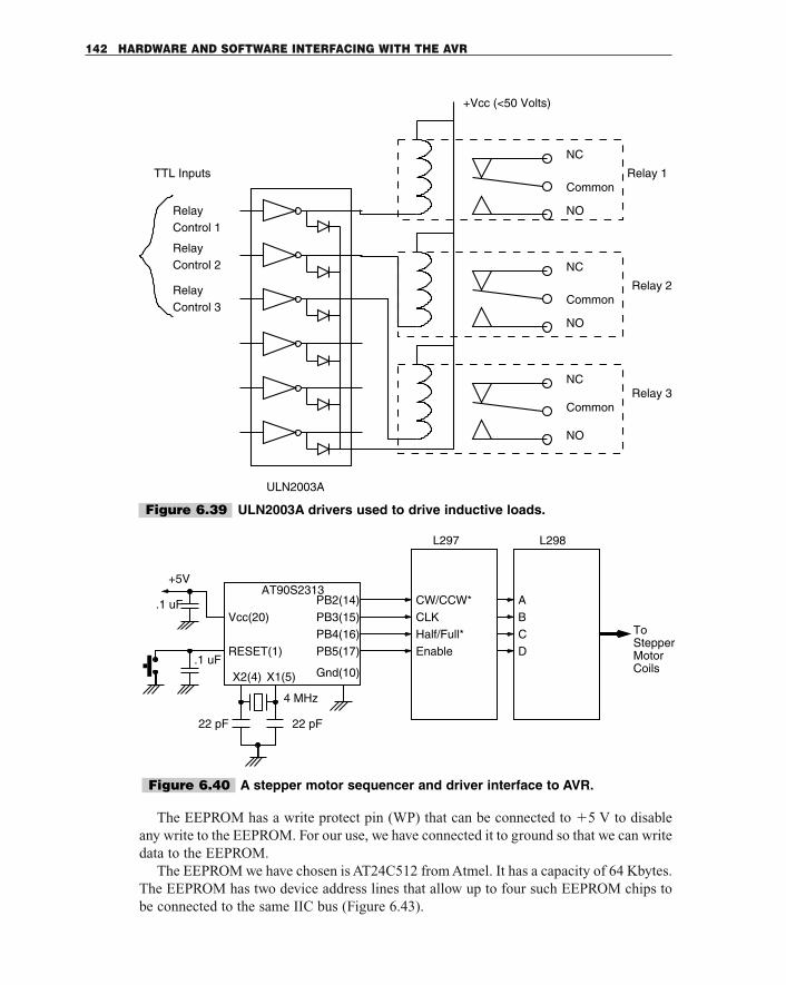
The EEPROM has a write protect pin (WP) that can be connected to �5 V to disableany write to the EEPROM. For our use, we have connected it to ground so that we can writedata to the EEPROM.
The EEPROM we have chosen is AT24C512 from Atmel. It has a capacity of 64 Kbytes.The EEPROM has two device address lines that allow up to four such EEPROM chips tobe connected to the same IIC bus (Figure 6.43).
142 HARDWARE AND SOFTWARE INTERFACING WITH THE AVR
ULN2003A
Relay 3
Relay 2
Relay 1TTL Inputs
Control 3Relay
Control 2Relay
Control 1Relay
NO
Common
NC
NO
Common
NC
NO
Common
NC
+Vcc (<50 Volts)
Figure 6.39 ULN2003A drivers used to drive inductive loads.
Vcc(20)
RESET(1)
Gnd(10)
22 pF22 pF
4 MHz
.1 uF
+5V
.1 uF
X2(4) X1(5)
AT90S2313
L297 L298
ToStepperMotorCoils
CW/CCW*CLKHalf/Full*Enable
ABCD
PB4(16)PB5(17)
PB3(15)PB2(14)
Figure 6.40 A stepper motor sequencer and driver interface to AVR.
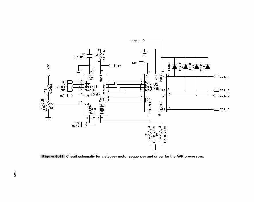
Figure 6.41 Circuit schematic for a stepper motor sequencer and driver for the AVR processors.
143
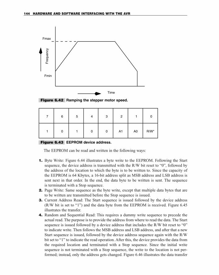
The EEPROM can be read and written in the following ways:
1. Byte Write: Figure 6.44 illustrates a byte write to the EEPROM. Following the Startsequence, the device address is transmitted with the R/W bit reset to “0”, followed bythe address of the location to which the byte is to be written to. Since the capacity ofthe EEPROM is 64 Kbytes, a 16-bit address split as MSB address and LSB address issent next in that order. In the end, the data byte to be written is sent. The sequence is terminated with a Stop sequence.
2. Page Write: Same sequence as the byte write, except that multiple data bytes that areto be written are transmitted before the Stop sequence is issued.
3. Current Address Read: The Start sequence is issued followed by the device address(R/W bit is set to “1”) and the data byte from the EEPROM is received. Figure 6.45illustrates the transfer.
4. Random and Sequential Read: This requires a dummy write sequence to precede theactual read. The purpose is to provide the address from where to read the data. The Startsequence is issued followed by a device address that includes the R/W bit reset to “0”to indicate write. Then follows the MSB address and LSB address, and after that a newStart sequence is issued, followed by the device address sequence again with the R/Wbit set to “1” to indicate the read operation. After this, the device provides the data fromthe required location and terminated with a Stop sequence. Since the initial writesequence is not terminated with a Stop sequence, the write to the location is not per-formed; instead, only the address gets changed. Figure 6.46 illustrates the data transfer
144 HARDWARE AND SOFTWARE INTERFACING WITH THE AVR
Time
Fre
quen
cy
Fmax
Fmin
Figure 6.42 Ramping the stepper motor speed.
7 6 5 4 3 2 1 0
1 0 1 0 0 A1 A0 R/W*
Figure 6.43 EEPROM device address.
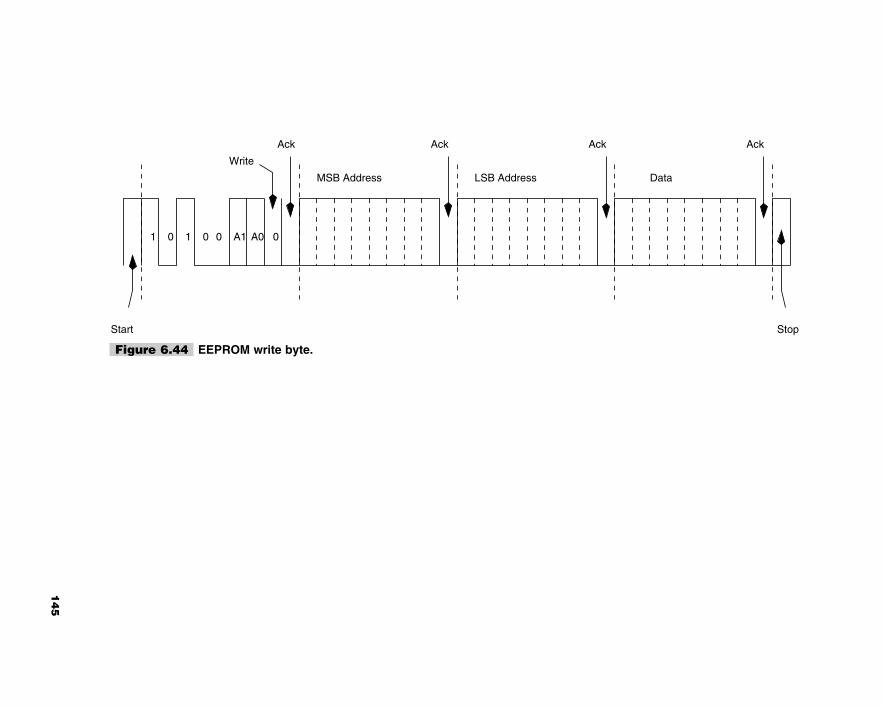
1 0 1 0 0 A1 A0 0
Start Stop
Ack Ack Ack Ack
MSB Address LSB Address Data
Write
Figure 6.44 EEPROM write byte.
14
5
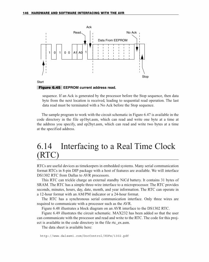
sequence. If an Ack is generated by the processor before the Stop sequence, then databyte from the next location is received, leading to sequential read operation. The lastdata read must be terminated with a No Ack before the Stop sequence.
The sample program to work with the circuit schematic in Figure 6.47 is available in thecode directory in the file ep1byt.asm, which can read and write one byte at a time at the address you specify, and ep2byt.asm, which can read and write two bytes at a time at the specified address.
6.14 Interfacing to a Real Time Clock(RTC)RTCs are useful devices as timekeepers in embedded systems. Many serial communicationformat RTCs in 8-pin DIP package with a host of features are available. We will interfaceDS1302 RTC from Dallas to AVR processors.
This RTC can trickle charge an external standby NiCd battery. It contains 31 bytes ofSRAM. The RTC has a simple three-wire interface to a microprocessor. The RTC providesseconds, minutes, hours, day, date, month, and year information. The RTC can operate ina 12-hour format with an AM/PM indicator or a 24-hour format.
The RTC has a synchronous serial communication interface. Only three wires arerequired to communicate with a processor such as the AVR.
Figure 6.48 illustrates a block diagram on an AVR interface to the DS1302 RTC.Figure 6.49 illustrates the circuit schematic. MAX232 has been added so that the user
can communicate with the processor and read and write to the RTC. The code for this proj-ect is available in the code directory in the file rtc_ex.asm.
The data sheet is available here:
http://www.dalsemi.com/DocControl/PDFs/1302.pdf
146 HARDWARE AND SOFTWARE INTERFACING WITH THE AVR
Start
Ack
Read
1 0 1 0 0 A1 A0 1
Data From EEPROM
No Ack
Stop
Figure 6.45 EEPROM current address read.
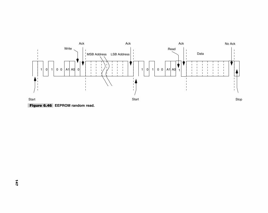
1 0 1 0 0 A1 A0 0
Start
Ack Ack
Write
1 0 1 0 0 A1 A0 1
Read
Start
MSB Address LSB Address
Stop
Ack
Data
No Ack
Figure 6.46 EEPROM random read.
14
7
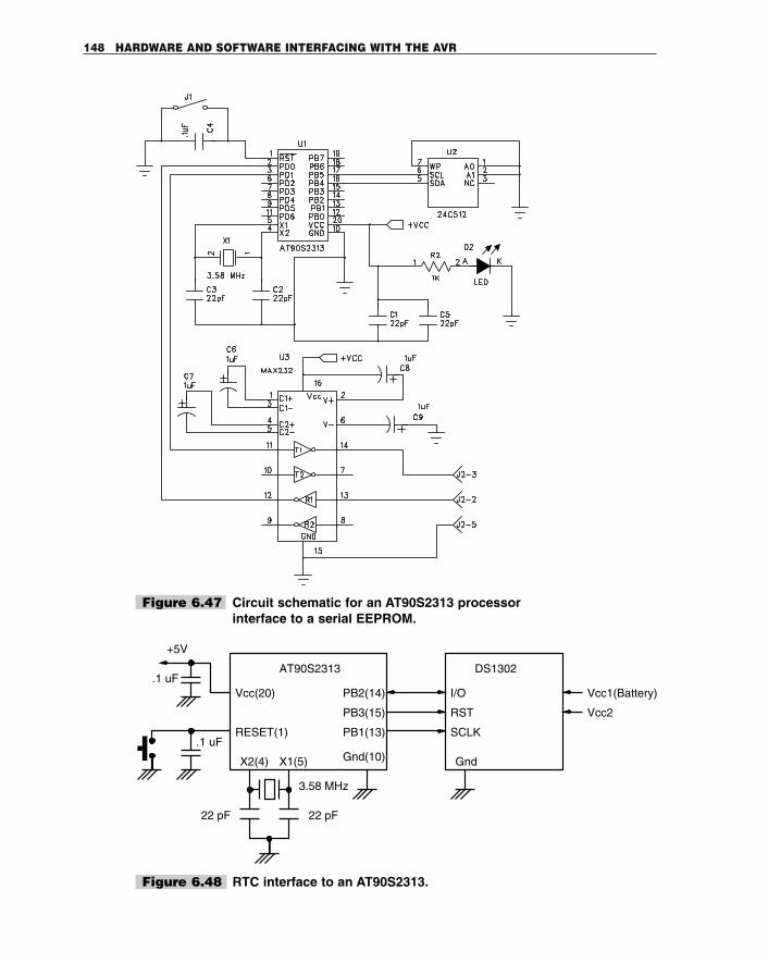
148 HARDWARE AND SOFTWARE INTERFACING WITH THE AVR
Figure 6.47 Circuit schematic for an AT90S2313 processorinterface to a serial EEPROM.
Vcc(20)
RESET(1)
Gnd(10)
22 pF22 pF
.1 uF
+5V
.1 uF
X2(4) X1(5)
AT90S2313
3.58 MHz
I/O
RST
SCLKPB1(13)
PB3(15)
PB2(14)
Gnd
Vcc1(Battery)
Vcc2
DS1302
Figure 6.48 RTC interface to an AT90S2313.
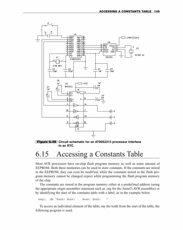
6.15 Accessing a Constants TableMost AVR processors have on-chip flash program memory as well as some amount ofEEPROM. Both these memories can be used to store constants. If the constants are storedin the EEPROM, they can even be modified, while the constants stored in the flash pro-gram memory cannot be changed expect while programming the flash program memoryof the chip.
The constants are stored in the program memory either at a predefined address (usingthe appropriate origin assembler statement such as .org for the Atmel’s AVR assembler) orby identifying the start of the constants table with a label, as in the example below.
msg1: .db “Honk! Honk! Honk! Honk! “
To access an individual element of the table, say the tenth from the start of the table, thefollowing program is used.
ACCESSING A CONSTANTS TABLE 149
Figure 6.49 Circuit schematic for an AT90S2313 processor interfaceto an RTC.
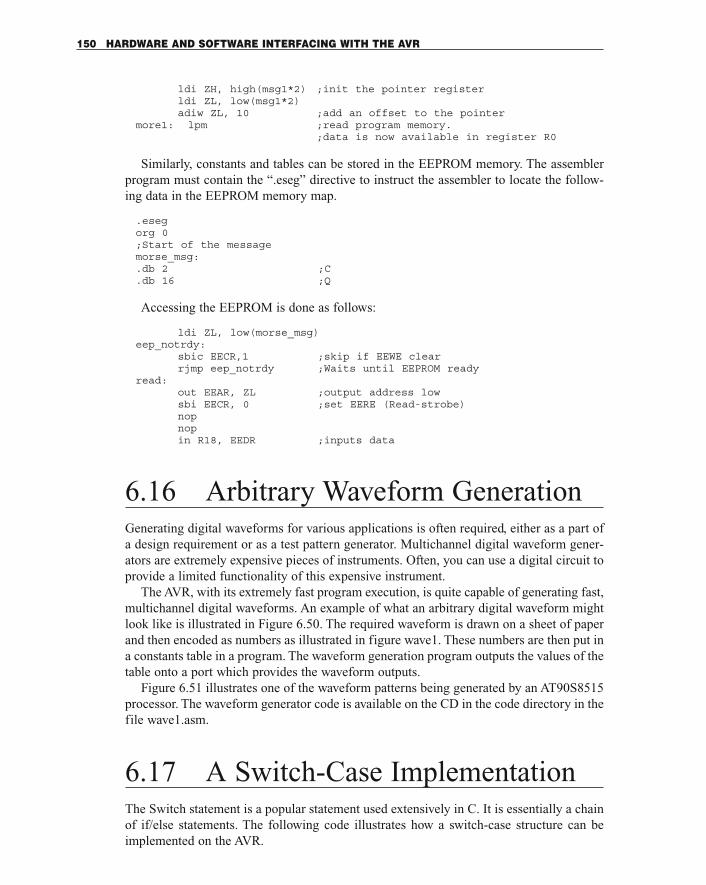
ldi ZH, high(msg1*2) ;init the pointer registerldi ZL, low(msg1*2)adiw ZL, 10 ;add an offset to the pointer
more1: lpm ;read program memory.;data is now available in register R0
Similarly, constants and tables can be stored in the EEPROM memory. The assemblerprogram must contain the “.eseg” directive to instruct the assembler to locate the follow-ing data in the EEPROM memory map.
.esegorg 0;Start of the messagemorse_msg:.db 2 ;C.db 16 ;Q
Accessing the EEPROM is done as follows:
ldi ZL, low(morse_msg)eep_notrdy:
sbic EECR,1 ;skip if EEWE clearrjmp eep_notrdy ;Waits until EEPROM ready
read:out EEAR, ZL ;output address lowsbi EECR, 0 ;set EERE (Read-strobe)nopnopin R18, EEDR ;inputs data
6.16 Arbitrary Waveform GenerationGenerating digital waveforms for various applications is often required, either as a part ofa design requirement or as a test pattern generator. Multichannel digital waveform gener-ators are extremely expensive pieces of instruments. Often, you can use a digital circuit toprovide a limited functionality of this expensive instrument.
The AVR, with its extremely fast program execution, is quite capable of generating fast,multichannel digital waveforms. An example of what an arbitrary digital waveform mightlook like is illustrated in Figure 6.50. The required waveform is drawn on a sheet of paperand then encoded as numbers as illustrated in figure wave1. These numbers are then put ina constants table in a program. The waveform generation program outputs the values of thetable onto a port which provides the waveform outputs.
Figure 6.51 illustrates one of the waveform patterns being generated by an AT90S8515processor. The waveform generator code is available on the CD in the code directory in thefile wave1.asm.
6.17 A Switch-Case ImplementationThe Switch statement is a popular statement used extensively in C. It is essentially a chainof if/else statements. The following code illustrates how a switch-case structure can beimplemented on the AVR.
150 HARDWARE AND SOFTWARE INTERFACING WITH THE AVR
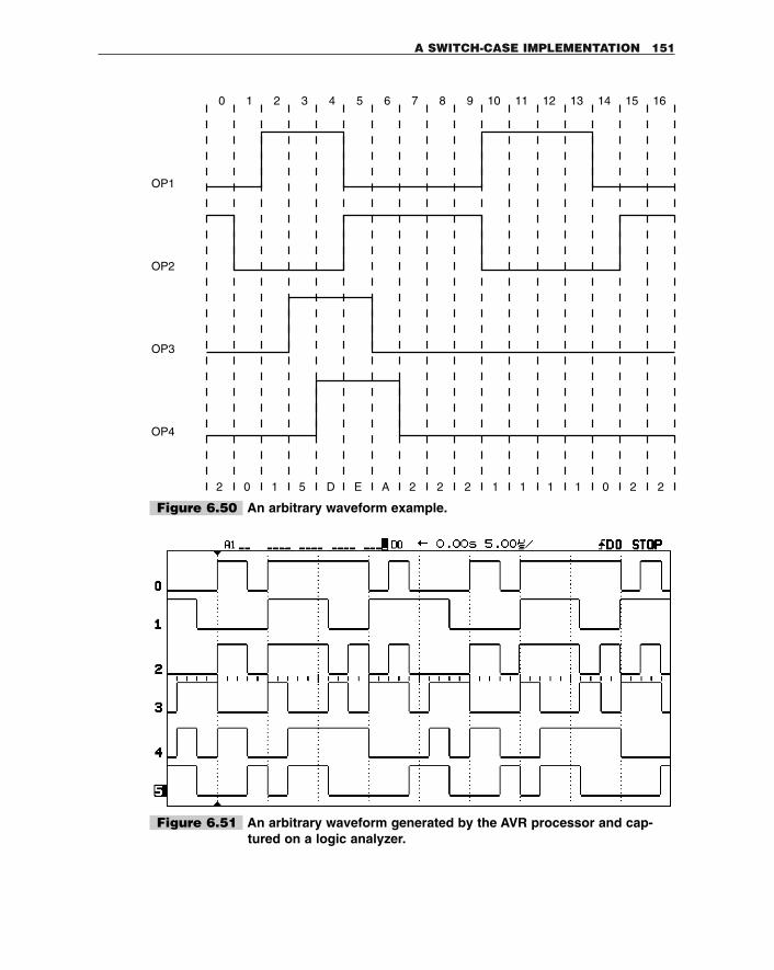
A SWITCH-CASE IMPLEMENTATION 151
0 1 2 3 4 5 6 7 8 9 10 11 12 13 14 15 16
OP1
OP3
OP4
OP2
A 2 2 2 1 1 1 1 0 2 22 0 1 5 D E
Figure 6.50 An arbitrary waveform example.
Figure 6.51 An arbitrary waveform generated by the AVR processor and cap-tured on a logic analyzer.
.equ option1=’A’
.equ option2=’B’
.equ option3=’C’
.equ option4=’D’
.equ option5=’E’
.equ option6=’F’
.def rreg=r18;***********************************************;Subroutine to implement a switch-case statememt;***********************************************sub_case: rcall get_byte ;get an argumentbegin_case: cpi rreg, option1 ;check if argu=option1
brne chk2 ;else compare with option2rcall sub_opt1 ;if yes execute subroutine
;sub_opt1chk2: cpi rreg, option2 ;check if argu=option2
brne chk3 ;else compare with option3rcall sub_opt2 ;if yes execute subroutine
;sub_opt2chk3: cpi rreg, option3 ;check if argu=option3
brne chk4 ;else compare with option4rcall sub_opt3 ;if yes execute subroutine
;sub_opt3chk4: cpi rreg, option4 ;check if argu=option4
brne chk5 ;else compare with option5rcall sub_opt4 ;if yes execute subroutine
;sub_opt4chk5: cpi rreg, option5 ;check if argu=option5
brne chk6 ;else compare with option6rcall sub_opt5 ;if yes execute subroutine
;sub_opt5chk6: cpi rreg, option6 ;check if argu=option6
brne chk_default ;nothing matches.rcall sub_opt6 ;if yes execute subroutine
;sub_opt6ret
chk_default: rcall sub_default ;else execute a default;subroutine
ret
6.18 Implementing a Finite StateMachineA finite state machine (FSM) is a formal concept with many applications. In general, afinite state machine is a device which has some inputs and some outputs. It stores the stateof the machine, and depending upon the inputs, changes the state value. The outputsdepend upon the state value. FSM has:
1. A set of finite states.2. Inputs.3. A transition function for each state.4. Outputs.
152 HARDWARE AND SOFTWARE INTERFACING WITH THE AVR
FSM has great applications in pattern recognition, vending machine applications, etc.You can create a traffic light controller modeled on the FSM concept.
The first step in modeling the requirement as an FSM is to create a state transition tableand an output table as illustrated in Tables 6.4 and 6.5. Another way is to create a bubblediagram description as illustrated in Figure 6.52. Some of the transitions from one state areconditional, while many others are unconditional. It is valid to have an FSM with allunconditional transitions. An ordinary binary counter is an example of an FSM withunconditional state transitions. The counter just hops from one state to the next and thenresets to the starting state. The minimum time for which the FSM remans in a state is deter-mined by the clock period of the system. In a microcontroller-based system, you could putappropriate delay routines between each transition.
The state of the FSM is maintained with the help of a variable (in a digital circuit, withthe help of a register). It is important that all the possible states of the register are account-ed for and, importantly, after power on, the register (or the variable) must be initializedwith a default state, otherwise the FSM will not work at all. A test code for implementinga finite state machine is available in the code directory in the file fsm.asm.
IMPLEMENTING A FINITE STATE MACHINE 153
TABLE 6-4 STATE TRANSITION
CURRENT STATE NEXT STATE (NS)
S0 X � 0 and Y � 0, NS � S1
SO X � 1, NS � S0
S1 X � 1 and Y � 0, NS � S2
S1 X�1 and Y � 1, NS � S3
S2 NS � S3
S3 NS � S4
S4 X � 1, NS � S4
S4 X � 0, NS � S0
TABLE 6-5 STATE OUTPUT
STATE OUTPUTS
SO A � 0, B � 23
S1 A � 1, B � 23
S2 A � 1, B � 32
S3 A � 0, B � 22
S4 A � 1, B � 44
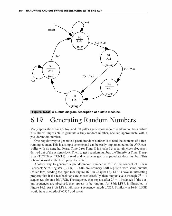
6.19 Generating Random NumbersMany applications such as toys and test pattern generators require random numbers. Whileit is almost impossible to generate a truly random number, one can approximate with apseudorandom number.
One popular way to generate a pseudorandom number is to read the contents of a free-running counter. This is a simple scheme and can be easily implemented on the AVR con-troller with no extra hardware. Timer0 (or Timer1) is clocked at a certain clock frequencyderived out of the system clock. Then, to get a random number, the Timer0 (or Timer1) reg-ister (TCNT0 or TCNT1) is read and what you get is a pseudorandom number. Thisscheme is used in the Dice project chapter.
Another way to generate a pseudorandom number is to use the concept of LinearFeedback Shift Register (LFSR). LFSRs are ordinary shift registers with some outputs(called taps) feeding the input (see Figure 16-3 in Chapter 16). LFSRs have an interestingproperty that if the feedback taps are chosen carefully, then outputs cycle through 2n � 1sequences, for an n-bit LFSR. The sequence then repeats after 2n � 1 instances. If the out-put sequences are observed, they appear to be random. An 8-bit LFSR is illustrated inFigure 16.3. An 8-bit LFSR will have a sequence length of 255. Similarly, a 16-bit LFSRwould have a length of 65535 and so on.
154 HARDWARE AND SOFTWARE INTERFACING WITH THE AVR
S0
S1
S2
S4
S3
A=0
B=23
A=1
B=23
X=0
X=1
X=1
A=1
B=32
A=0
B=22
A=1
B=44
X=0, Y=0
X=1, Y=0
X=1, Y=1
Reset
Figure 6.52 A bubble diagram description of a state machine.
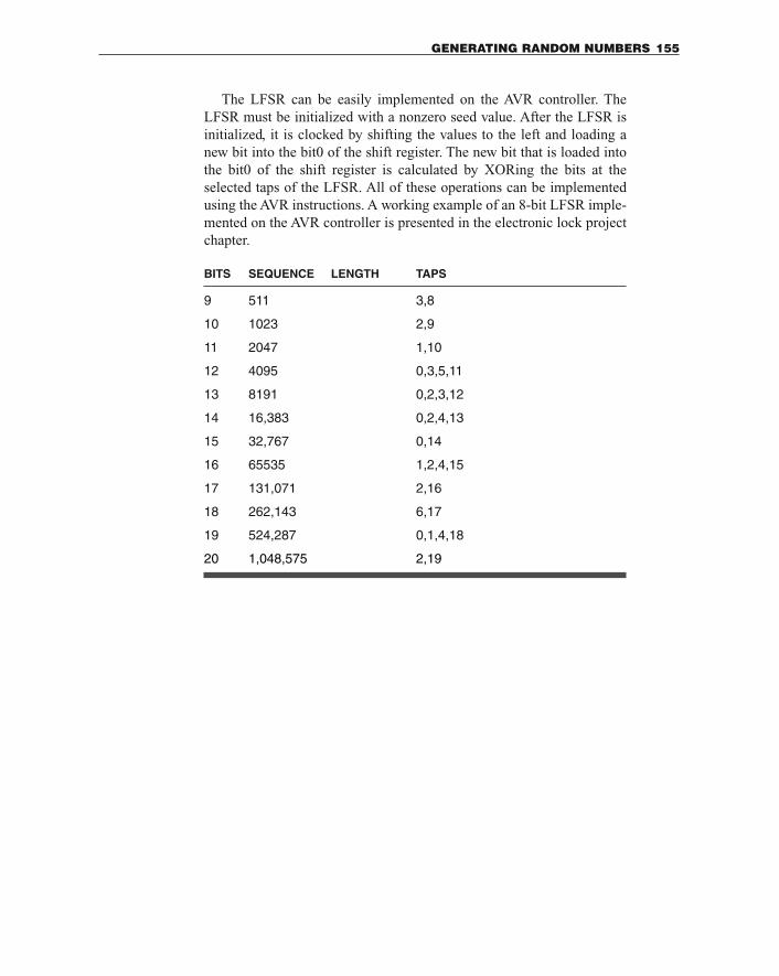
GENERATING RANDOM NUMBERS 155
The LFSR can be easily implemented on the AVR controller. TheLFSR must be initialized with a nonzero seed value. After the LFSR isinitialized, it is clocked by shifting the values to the left and loading anew bit into the bit0 of the shift register. The new bit that is loaded intothe bit0 of the shift register is calculated by XORing the bits at theselected taps of the LFSR. All of these operations can be implementedusing the AVR instructions. A working example of an 8-bit LFSR imple-mented on the AVR controller is presented in the electronic lock projectchapter.
BITS SEQUENCE LENGTH TAPS
9 511 3,8
10 1023 2,9
11 2047 1,10
12 4095 0,3,5,11
13 8191 0,2,3,12
14 16,383 0,2,4,13
15 32,767 0,14
16 65535 1,2,4,15
17 131,071 2,16
18 262,143 6,17
19 524,287 0,1,4,18
20 1,048,575 2,19

This page intentionally left blank.
7.1 IntroductionNo man is an island, and neither is a microcontroller application. Except for those thatare completely self-contained in a single chip microcontroller, your microcontroller-basedapplication will need to communicate with an external device, be it an additional periph-eral device, a host PC, or another microcontroller-based application. Figure 7.1 illustratesthe idea.
In the simplest of cases, the AVR device communicates to a peripheral device such asa memory device, or a digital port or an ADC. These devices may be part of a single appli-cation. In another case, your AVR device may want to communicate with a host PC fortransferring data, while in another case, it may want to communicate to multiple devicesall interconnected to each other using a bus configuration.
The communication between an AVR and an external device or devices is essentially oftwo types: point-to-point communication or a bus-based communication. A point-to-pointcommunication connects two devices, while a bus offers multiple devices to share the samephysical connection lines.
Whether to go for a point-to-point communication or a bus-based communication issolely determined by need. Bus-based communication seems attractive, as a single com-munication link allows multiple devices to communicate, but this scheme is not withoutcomplexities—for example to regulate communication traffic on the shared lines.
7COMMUNICATION LINKS
FOR THE AVR PROCESSOR
157
Copyright 2001 The McGraw-Hill Companies, Inc. Click Here for Terms of Use.
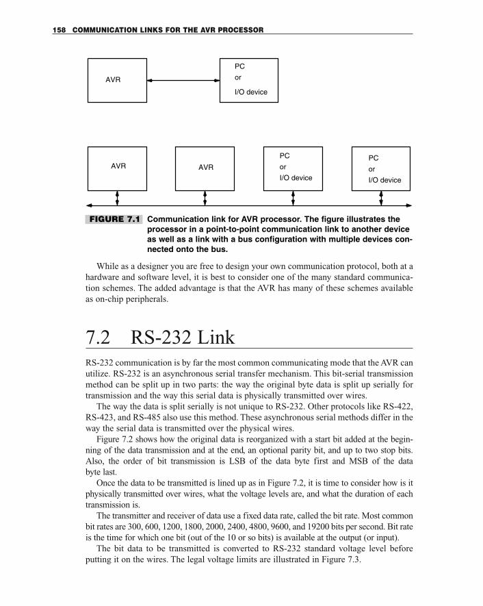
While as a designer you are free to design your own communication protocol, both at ahardware and software level, it is best to consider one of the many standard communica-tion schemes. The added advantage is that the AVR has many of these schemes availableas on-chip peripherals.
7.2 RS-232 LinkRS-232 communication is by far the most common communicating mode that the AVR canutilize. RS-232 is an asynchronous serial transfer mechanism. This bit-serial transmissionmethod can be split up in two parts: the way the original byte data is split up serially fortransmission and the way this serial data is physically transmitted over wires.
The way the data is split serially is not unique to RS-232. Other protocols like RS-422,RS-423, and RS-485 also use this method. These asynchronous serial methods differ in theway the serial data is transmitted over the physical wires.
Figure 7.2 shows how the original data is reorganized with a start bit added at the begin-ning of the data transmission and at the end, an optional parity bit, and up to two stop bits.Also, the order of bit transmission is LSB of the data byte first and MSB of the data byte last.
Once the data to be transmitted is lined up as in Figure 7.2, it is time to consider how is itphysically transmitted over wires, what the voltage levels are, and what the duration of eachtransmission is.
The transmitter and receiver of data use a fixed data rate, called the bit rate. Most commonbit rates are 300, 600, 1200, 1800, 2000, 2400, 4800, 9600, and 19200 bits per second. Bit rateis the time for which one bit (out of the 10 or so bits) is available at the output (or input).
The bit data to be transmitted is converted to RS-232 standard voltage level beforeputting it on the wires. The legal voltage limits are illustrated in Figure 7.3.
158 COMMUNICATION LINKS FOR THE AVR PROCESSOR
AVR
I/O device
PC
or
AVR AVR
PC
or
I/O device
PC
or
I/O device
FIGURE 7.1 Communication link for AVR processor. The figure illustrates theprocessor in a point-to-point communication link to another deviceas well as a link with a bus configuration with multiple devices con-nected onto the bus.
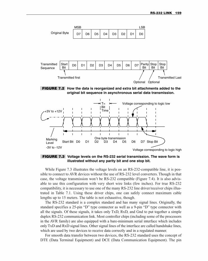
While Figure 7.3 illustrates the voltage levels on an RS-232-compatible line, it is pos-sible to connect to AVR devices without the use of RS-232 level converters. Though in thatcase, the voltage transmission won’t be RS-232 compatible (Figure 7.4). It is also advis-able to use this configuration with very short wire links (few inches). For true RS-232compatibility, it is necessary to use one of the many RS-232 line driver/receiver chips illus-trated in Table 7.1. Using these driver chips, one can safely connect maximum cablelengths up to 15 meters. The table is not exhaustive, though.
The RS-232 standard is a complex standard and has many signal lines. Originally, thestandard specifies a 25-pin “D” type connector as well as a 9-pin “D” type connector withall the signals. Of these signals, it takes only TxD, RxD, and Gnd to put together a simpleduplex RS-232 communication link. Most controller chips (including some of the processorsin the AVR family) are also equipped with a bare-minimum serial interface which includesonly TxD and RxD signal lines. Other signal lines of the interface are called handshake lines,which are used by two devices to receive data correctly and in a regulated manner.
For smooth data transfer between two devices, the RS-232 standard uses the concept ofDTE (Data Terminal Equipment) and DCE (Data Communication Equipment). The pin
RS-232 LINK 159
D0D1D2D3D4D5D6D7
LSBMSB
Original Byte
Transmitted Sequence
Transmitted firstOptional
Start D0 D1 D2 D3 D4 D5 D6 D7 StopBit
ParityBit Bit
StopBit
Transmitted LastOptional
FIGURE 7.2 How the data is reorganized and extra bit attachments added to theoriginal bit sequence in asynchronous serial data transmission.
T=BitTime
MarkingLevel
+3V to +12V
-3V to -12V
One byte transmissionStart Bit D0 D1 D2 D3 D4 D5 D6 D7 Stop Bit
Voltage corresponding to logic low
Voltage corresponding to logic high
FIGURE 7.3 Voltage levels on the RS-232 serial transmission. The wave form isillustrated without any parity bit and one stop bit.
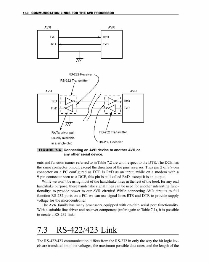
TxD
RxD
AVR
RxD
TxD
AVR
TxD
AVR
RxD
RxD
TxD
AVR
RS-232 Transmitter
RS-232 Transmitter
RS-232 Receiver
RS-232 Receiver
Rx/Tx driver pair
usually available
in a single chip
FIGURE 7.4 Connecting an AVR device to another AVR orany other serial device.
outs and function names referred to in Table 7.2 are with respect to the DTE. The DCE hasthe same connector pinout, except the direction of the pins reverses. Thus pin 2 of a 9-pinconnector on a PC configured as DTE is RxD as an input, while on a modem with a 9-pin connector seen as a DCE, this pin is still called RxD, except it is an output.
While we won’t be using most of the handshake lines in the rest of the book for any realhandshake purpose, these handshake signal lines can be used for another interesting func-tionality: to provide power to our AVR circuits! While connecting AVR circuits to fullfunction RS-232 ports on a PC, we can use signal lines RTS and DTR to provide supplyvoltage for the microcontroller.
The AVR family has many processors equipped with on-chip serial port functionality.With a suitable line driver and receiver component (refer again to Table 7.1), it is possibleto create a RS-232 link.
7.3 RS-422/423 LinkThe RS-422/423 communication differs from the RS-232 in only the way the bit logic lev-els are translated into line voltages, the maximum possible data rates, and the length of the
160 COMMUNICATION LINKS FOR THE AVR PROCESSOR
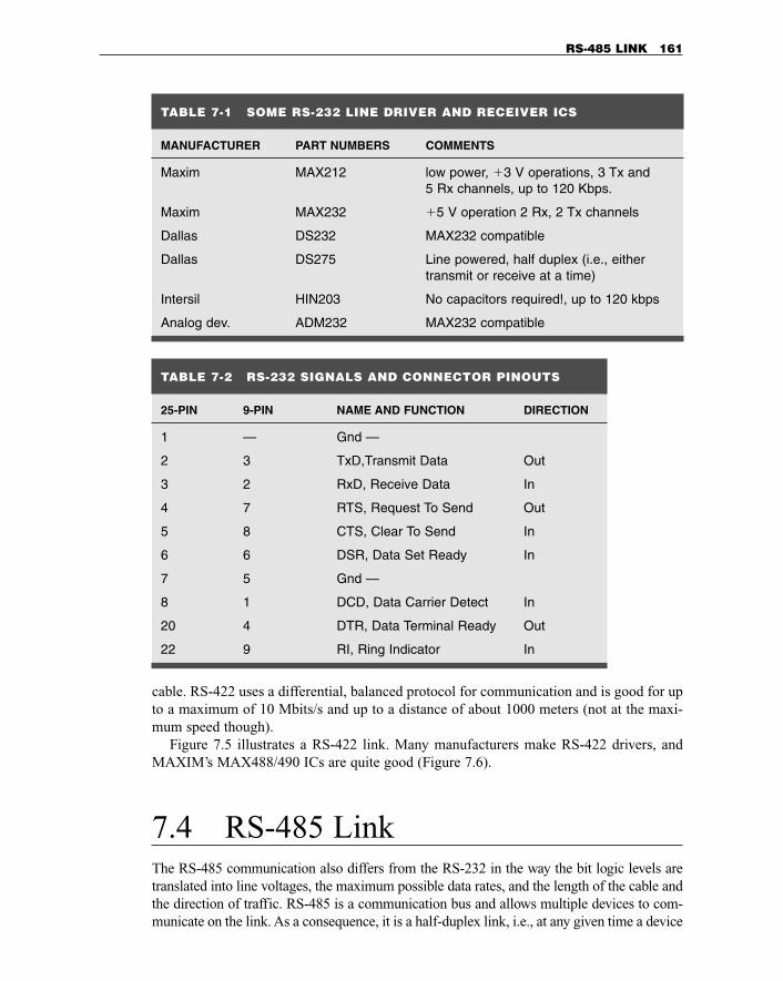
RS-485 LINK 161
cable. RS-422 uses a differential, balanced protocol for communication and is good for upto a maximum of 10 Mbits/s and up to a distance of about 1000 meters (not at the maxi-mum speed though).
Figure 7.5 illustrates a RS-422 link. Many manufacturers make RS-422 drivers, andMAXIM’s MAX488/490 ICs are quite good (Figure 7.6).
7.4 RS-485 LinkThe RS-485 communication also differs from the RS-232 in the way the bit logic levels aretranslated into line voltages, the maximum possible data rates, and the length of the cable andthe direction of traffic. RS-485 is a communication bus and allows multiple devices to com-municate on the link. As a consequence, it is a half-duplex link, i.e., at any given time a device
TABLE 7-2 RS-232 SIGNALS AND CONNECTOR PINOUTS
25-PIN 9-PIN NAME AND FUNCTION DIRECTION
1 — Gnd —
2 3 TxD,Transmit Data Out
3 2 RxD, Receive Data In
4 7 RTS, Request To Send Out
5 8 CTS, Clear To Send In
6 6 DSR, Data Set Ready In
7 5 Gnd —
8 1 DCD, Data Carrier Detect In
20 4 DTR, Data Terminal Ready Out
22 9 RI, Ring Indicator In
TABLE 7-1 SOME RS-232 LINE DRIVER AND RECEIVER ICS
MANUFACTURER PART NUMBERS COMMENTS
Maxim MAX212 low power, �3 V operations, 3 Tx and 5 Rx channels, up to 120 Kbps.
Maxim MAX232 �5 V operation 2 Rx, 2 Tx channels
Dallas DS232 MAX232 compatible
Dallas DS275 Line powered, half duplex (i.e., either transmit or receive at a time)
Intersil HIN203 No capacitors required!, up to 120 kbps
Analog dev. ADM232 MAX232 compatible
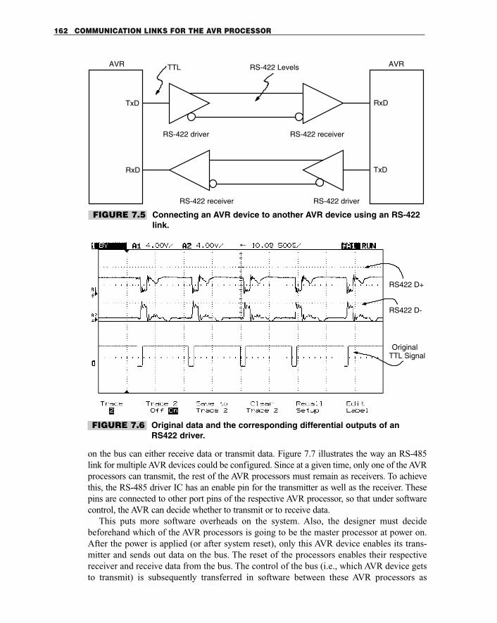
162 COMMUNICATION LINKS FOR THE AVR PROCESSOR
AVR AVRTTL RS-422 Levels
RxD
TxD
TxD
RxD
RS-422 driverRS-422 receiver
RS-422 driver RS-422 receiver
FIGURE 7.5 Connecting an AVR device to another AVR device using an RS-422link.
RS422 D+
RS422 D-
OriginalTTL Signal
FIGURE 7.6 Original data and the corresponding differential outputs of anRS422 driver.
on the bus can either receive data or transmit data. Figure 7.7 illustrates the way an RS-485link for multiple AVR devices could be configured. Since at a given time, only one of the AVRprocessors can transmit, the rest of the AVR processors must remain as receivers. To achievethis, the RS-485 driver IC has an enable pin for the transmitter as well as the receiver. Thesepins are connected to other port pins of the respective AVR processor, so that under softwarecontrol, the AVR can decide whether to transmit or to receive data.
This puts more software overheads on the system. Also, the designer must decidebeforehand which of the AVR processors is going to be the master processor at power on.After the power is applied (or after system reset), only this AVR device enables its trans-mitter and sends out data on the bus. The reset of the processors enables their respectivereceiver and receive data from the bus. The control of the bus (i.e., which AVR device getsto transmit) is subsequently transferred in software between these AVR processors as
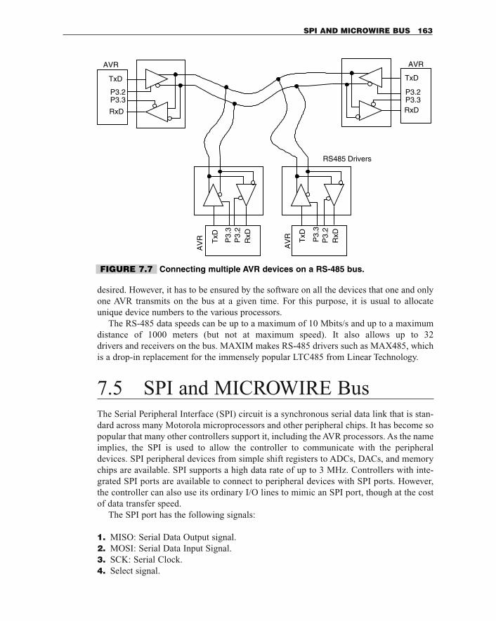
SPI AND MICROWIRE BUS 163
desired. However, it has to be ensured by the software on all the devices that one and onlyone AVR transmits on the bus at a given time. For this purpose, it is usual to allocateunique device numbers to the various processors.
The RS-485 data speeds can be up to a maximum of 10 Mbits/s and up to a maximumdistance of 1000 meters (but not at maximum speed). It also allows up to 32 drivers and receivers on the bus. MAXIM makes RS-485 drivers such as MAX485, whichis a drop-in replacement for the immensely popular LTC485 from Linear Technology.
7.5 SPI and MICROWIRE BusThe Serial Peripheral Interface (SPI) circuit is a synchronous serial data link that is stan-dard across many Motorola microprocessors and other peripheral chips. It has become sopopular that many other controllers support it, including the AVR processors. As the nameimplies, the SPI is used to allow the controller to communicate with the peripheraldevices. SPI peripheral devices from simple shift registers to ADCs, DACs, and memorychips are available. SPI supports a high data rate of up to 3 MHz. Controllers with inte-grated SPI ports are available to connect to peripheral devices with SPI ports. However,the controller can also use its ordinary I/O lines to mimic an SPI port, though at the costof data transfer speed.
The SPI port has the following signals:
1. MISO: Serial Data Output signal.2. MOSI: Serial Data Input Signal.3. SCK: Serial Clock.4. Select signal.
AVR
RxD
TxD
RxD
TxD TxD
RxD
TxD
RxD
AVR
AV
R
RS485 Drivers
P3.2P3.3
P3.2P3.3
P3.
3P
3.2
P3.
3P
3.2
AV
R
FIGURE 7.7 Connecting multiple AVR devices on a RS-485 bus.
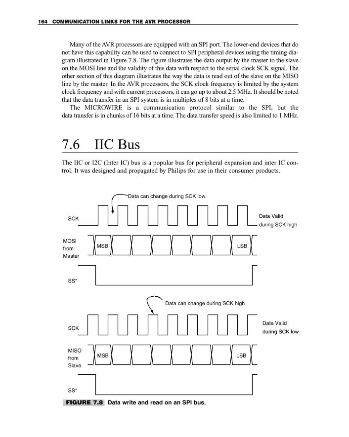
164 COMMUNICATION LINKS FOR THE AVR PROCESSOR
SS*
MSB LSB
MSB LSB
SCK
SS*
SCK
Masterfrom MOSI
MISO
Slavefrom
Data Valid
during SCK high
Data Valid
during SCK low
Data can change during SCK low
Data can change during SCK high
FIGURE 7.8 Data write and read on an SPI bus.
Many of the AVR processors are equipped with an SPI port. The lower-end devices that donot have this capability can be used to connect to SPI peripheral devices using the timing dia-gram illustrated in Figure 7.8. The figure illustrates the data output by the master to the slaveon the MOSI line and the validity of this data with respect to the serial clock SCK signal. Theother section of this diagram illustrates the way the data is read out of the slave on the MISOline by the master. In the AVR processors, the SCK clock frequency is limited by the systemclock frequency and with current processors, it can go up to about 2.5 MHz. It should be notedthat the data transfer in an SPI system is in multiples of 8 bits at a time.
The MICROWIRE is a communication protocol similar to the SPI, but the data transfer is in chunks of 16 bits at a time. The data transfer speed is also limited to 1 MHz.
7.6 IIC BusThe IIC or I2C (Inter IC) bus is a popular bus for peripheral expansion and inter IC con-trol. It was designed and propagated by Philips for use in their consumer products.
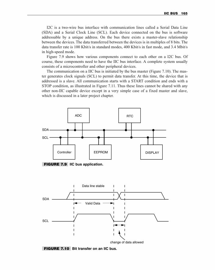
IIC BUS 165
I2C is a two-wire bus interface with communication lines called a Serial Data Line(SDA) and a Serial Clock Line (SCL). Each device connected on the bus is softwareaddressable by a unique address. On the bus there exists a master-slave relationshipbetween the devices. The data transferred between the devices is in multiples of 8 bits. Thedata transfer rate is 100 Kbit/s in standard modes, 400 Kbit/s in fast mode, and 3.4 Mbit/sin high-speed mode.
Figure 7.9 shows how various components connect to each other on a I2C bus. Ofcourse, these components need to have the IIC bus interface. A complete system usuallyconsists of a microcontroller and other peripheral devices.
The communication on a IIC bus is initiated by the bus master (Figure 7.10). The mas-ter generates clock signals (SCL) to permit data transfer. At this time, the device that isaddressed is a slave. All communication starts with a START condition and ends with aSTOP condition, as illustrated in Figure 7.11. Thus these lines cannot be shared with anyother non-IIC capable device except in a very simple case of a fixed master and slave,which is discussed in a later project chapter.
SDA
SCL
ADC RTC
Controller EEPROM DISPLAY
FIGURE 7.9 IIC bus application.
SDA
SCL
Data line stable
Valid Data
change of data allowed
FIGURE 7.10 Bit transfer on an IIC bus.
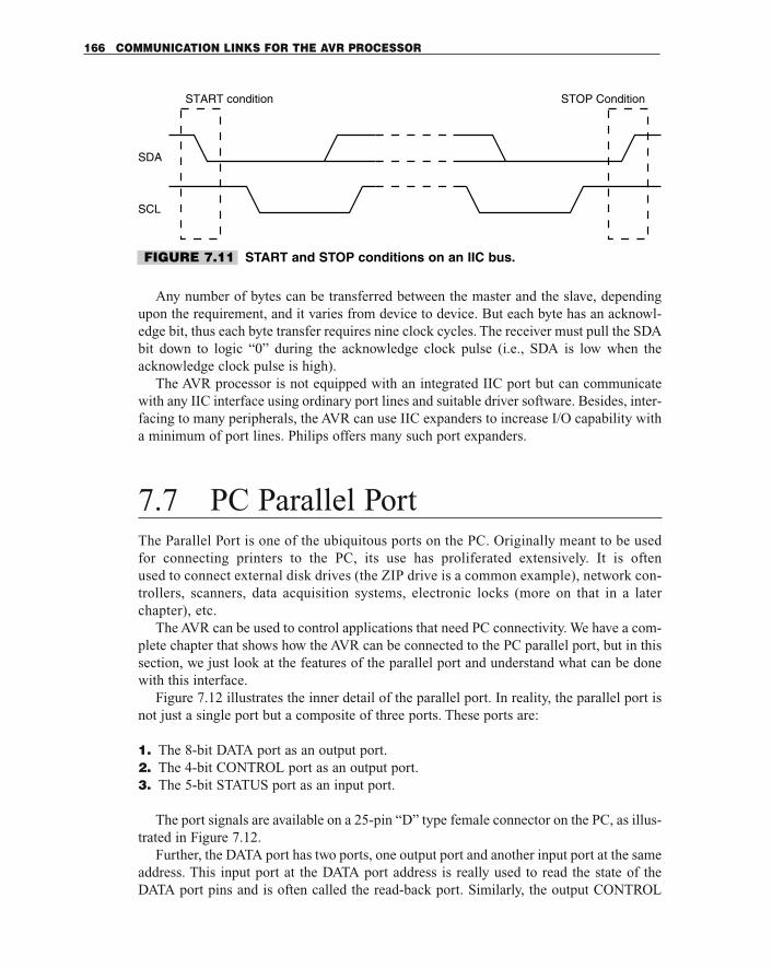
166 COMMUNICATION LINKS FOR THE AVR PROCESSOR
Any number of bytes can be transferred between the master and the slave, dependingupon the requirement, and it varies from device to device. But each byte has an acknowl-edge bit, thus each byte transfer requires nine clock cycles. The receiver must pull the SDAbit down to logic “0” during the acknowledge clock pulse (i.e., SDA is low when theacknowledge clock pulse is high).
The AVR processor is not equipped with an integrated IIC port but can communicatewith any IIC interface using ordinary port lines and suitable driver software. Besides, inter-facing to many peripherals, the AVR can use IIC expanders to increase I/O capability witha minimum of port lines. Philips offers many such port expanders.
7.7 PC Parallel PortThe Parallel Port is one of the ubiquitous ports on the PC. Originally meant to be usedfor connecting printers to the PC, its use has proliferated extensively. It is often used to connect external disk drives (the ZIP drive is a common example), network con-trollers, scanners, data acquisition systems, electronic locks (more on that in a later chapter), etc.
The AVR can be used to control applications that need PC connectivity. We have a com-plete chapter that shows how the AVR can be connected to the PC parallel port, but in thissection, we just look at the features of the parallel port and understand what can be donewith this interface.
Figure 7.12 illustrates the inner detail of the parallel port. In reality, the parallel port isnot just a single port but a composite of three ports. These ports are:
1. The 8-bit DATA port as an output port.2. The 4-bit CONTROL port as an output port.3. The 5-bit STATUS port as an input port.
The port signals are available on a 25-pin “D” type female connector on the PC, as illus-trated in Figure 7.12.
Further, the DATA port has two ports, one output port and another input port at the sameaddress. This input port at the DATA port address is really used to read the state of theDATA port pins and is often called the read-back port. Similarly, the output CONTROL
START condition STOP Condition
SDA
SCL
FIGURE 7.11 START and STOP conditions on an IIC bus.
port also has an input port at the same address and is used to read the status of the CON-TROL port pins. So, in reality the parallel port has five ports.
Figure 7.13 illustrates the detail of the DATA port. The figure shows the internal PC busconnected to an output latch. The outputs of this latch are the DATA port outputs.Similarly, these 8 bits of the data port are also connected to the input of a buffer, whichconnects to the PC bus. Thus a program running on the PC could output any combinationof 8 bits on the DATA port through the output DATA port and, when required, read thiscombination back through the corresponding input port.
It is easy to access the DATA port either for sending data out or reading the state of theDATA port pins using a C program running on the PC. However, to be able to send data toor read data from any port on the PC, it is essential to know the port address. These portaddresses are not completely fixed. Different PCs may have different addresses. Ratherthan guess the address values, the user can find out the actual port addresses in a PC byreading the contents of certain RAM locations called BIOS data area (the address off theseRAM locations is known and fixed!). For the PC parallel port, the RAM address is0040:0008 (hex) for LPT1, 0040:000a (hex) for LPT2, and 0040:000c (hex) for LPT3. Ina particular PC, if the number found in these locations turns out to be zero, then it meansthat the corresponding LPT does not exist on the PC. A nonzero number on these locationsindicates that the corresponding LPT exists. This number is the base address of the paral-lel port. The port addresses of the various ports are as follows:
PC PARALLEL PORT 167
IRQ Enable
OE*
OE*
OE*
#3
#2
#2
#1#1
Tri-state buffer #4
IRQ5 / IRQ7
IOR*, IOW*
A9 to A0
Status Read
Control Read
Control Write
Data Read
Data Write
output Connector25 Pin D type
(4 bits)
(8 bits)Data Port
Buffer
Buffer
DriversOCLatch
LatchBufferData Bus (D7:D0)
CommandDecoder
BitsAddress
BitsControl
BitsData
BusSystem
PC
Control Port
Status Port(5 bits)
FIGURE 7.12 The details of the PC parallel port.
1. DATA Port � Base Address2. STATUS Port � Base Address � 13. CONTROL Port � Base Address � 2
I will show some C code to do various things with the parallel port in this section. Toread the base address and to calculate the port addresses of the various ports of the paral-lel port, do the following:
int offset, DATAport, STATUSport, CONTROLport, BASEaddress;offset = 0x08; /*0x08 for LPT1, 0x0a for LPT2, 0x0c for LPT3*/BASEaddress = peek(0x40, offset); /*read the address from BIOS dataarea*/DATAport = BASEaddress; /* address of DATA port*/STATUSport = BASEaddress + 1; /*address of STATUS port*/CONTROLport = BASEaddress + 2; /*address of CONTROL port*/
To write some value to the DATA port pins, we do the following:int offset, DATAport, STATUSport, CONTROLport, BASEaddress;unsigned char data_value;data_value = 0x55;/*write a binary sequence 01010101 on the DATA port pins*/outportb(DATAport, data_value);To read the state of the DATA port pins, we do the following:
int offset, DATAport, STATUSport, CONTROLport, BASEaddress;unsigned char data_pins;data_pins = inportb(DATAport);printf(``\nThe DATA pins have the value = %x’’, data_pins);
168 COMMUNICATION LINKS FOR THE AVR PROCESSOR
EnableOutput
Output EnableClock DATA7
DATA6
DATA5
DATA4
DATA3
DATA2
DATA1
DATA0
C=.0022 uF
R=27 Ohms
Data Read
Data Write
DecoderCommand
BusData
PC System
2
3
4
5
6
7
8
9
74LS37474LS244
Output Connectorpins
FIGURE 7.13 The DATA port.
Figure 7.14 illustrates the detail of the STATUS port. The figure shows the internal PCbus connected to an input buffer. The inputs of this buffer (some are through inverters) arethe STATUS port inputs. The STATUS port has 5 inputs only connected to the upper 5 bitsof the 8-bit port. The STATUS port is used to read external data into the PC.
The following code shows how to read external data from the STATUS port and how topress the date to account for the inversions on certain bits.
int STATUSport;unsigned char status_pins;status_pins=inportb(STATUSport) & 0xf8;printf(““\nActual STATUS port = %X’’, status_pins);printf(““\nSTATUS port shifted = %X’’, status_pins}}3);printf(““\nSTATUS port shifted and corrected = %X’’, 0x10(status_pins>>3));
Figure 7.15 shows the block diagram for the CONTROL port of the parallel port. TheCONTROL port has 4 bits which are placed in the lower 4 bits of a byte. Of the 4 bits, 3of the bits are inverted before being output of the port pins. These pins are also read backthrough an inverting buffer. An inverter on one of the lines accounts for the signal inver-sion on the output lines, and if this buffer is read, it provides the bit information that wasoriginally sent to the CONTROL port.
PC PARALLEL PORT 169
S3
S4
S5
S6
S7*
bit 4 (IRQ EN)CONTROL portFrom
or IRQ7To IRQ5
PinsOutput D type Connector
nERROR
SELECT
PE
nACK
BUSY
D3
D4
D5
D6
D7
PC System Data Bus
Command Decoder
74LS240
Status Read
EnableOutput
11
10
12
13
15
74LS126
FIGURE 7.14 The STATUS port.
>
The data can be sent on the CONTROL port in the same manner as the DATA port(except that the port address is at an offset of two from the base address) and the CON-TROL port data is read back in the same manner as the data is read on the STATUS port,again with the offest of two from the base address.
Table 7.3 illustrates the signals, connector pin numbers, and functions of all the paral-lel port signals. A working example of interfacing an AVR processor to the parallel port isillustrated in a later chapter as a project.
There is a simple arrangement to connect an AVR processor and the parallel port(Figure 7.16). This mechanism allows 4 bits to be transferred between the parallel port andthe AVR. We have chosen the CONTROL port, as it can be used both for data output anddata input. To output data, appropriate data is written to the CONTROL port and whenreading data, first the CONTROL port bits are all set to “1” (logic high), and then the readbuffer (at the same address as the CONTROL port) on the CONTROL port is read. Theread value (after correction for the inverters) is the value output by the AVR.
One of the STATUS port lines is used by the parallel port as one of the input handshakelines. The output handshake line is by using the DATA port pin as illustrated.
170 COMMUNICATION LINKS FOR THE AVR PROCESSOR
clock
C = .0022 uF
C
Control Read
Control Write
Command Decoder
D4
D0
D1
D2
D3
D4D3
D2
D1
D0
Data BusPC System
74LS240
74LS126
EnableOutput
IRQ EN (bit C4)
pinsOutput connector
C3*
C2
C1*
C0*
17
16
14
1
I
OCI
OCI
OCI
OCI
I
74LS174
+5V
R=4K7R= 27 Ohm
FIGURE 7.15 The CONTROL port.
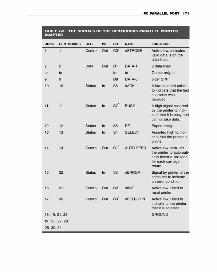
PC PARALLEL PORT 171
TABLE 7-3 THE SIGNALS OF THE CENTRONICS PARALLEL PRINTERADAPTER
DB-25 CENTRONICS REG. I/O BIT NAME FUNCTION
1 1 Control Out C0* nSTROBE Active low. Indicatesvalid data is on thedata lines.
2 2 Data Out D1 DATA-1 8 data lines
to to to to Output only in
9 9 D8 DATA-8 older SPP
10 10 Status In S6 nACK A low asserted pulseto indicate that the lastcharacter wasreceived.
11 11 Status In S7* BUSY A high signal assertedby the printer to indi-cate that it is busy andcannot take data.
12 12 Status In S5 PE Paper empty
13 13 Status In S4 SELECT Asserted high to indi-cate that the printer isonline
14 14 Control Out C1* AUTO FEED Active low. Instructsthe printer to automati-cally insert a line feedfor each carriagereturn.
15 32 Status In S3 nERROR Signal by printer to thecomputer to indicatean error condition.
16 31 Control Out C2 nINIT Active low. Used toreset printer
17 36 Control Out C3* nSELECTIN Active low. Used toindicate to the printerthat it is selected
18, 19, 21, 23 GROUND
to 25, 27, 29
25 30, 34
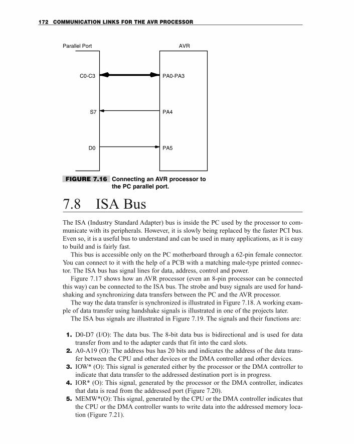
7.8 ISA BusThe ISA (Industry Standard Adapter) bus is inside the PC used by the processor to com-municate with its peripherals. However, it is slowly being replaced by the faster PCI bus.Even so, it is a useful bus to understand and can be used in many applications, as it is easyto build and is fairly fast.
This bus is accessible only on the PC motherboard through a 62-pin female connector.You can connect to it with the help of a PCB with a matching male-type printed connec-tor. The ISA bus has signal lines for data, address, control and power.
Figure 7.17 shows how an AVR processor (even an 8-pin processor can be connectedthis way) can be connected to the ISA bus. The strobe and busy signals are used for hand-shaking and synchronizing data transfers between the PC and the AVR processor.
The way the data transfer is synchronized is illustrated in Figure 7.18. A working exam-ple of data transfer using handshake signals is illustrated in one of the projects later.
The ISA bus signals are illustrated in Figure 7.19. The signals and their functions are:
1. D0-D7 (I/O): The data bus. The 8-bit data bus is bidirectional and is used for datatransfer from and to the adapter cards that fit into the card slots.
2. A0-A19 (O): The address bus has 20 bits and indicates the address of the data trans-fer between the CPU and other devices or the DMA controller and other devices.
3. IOW* (O): This signal is generated either by the processor or the DMA controller toindicate that data transfer to the addressed destination port is in progress.
4. IOR* (O): This signal, generated by the processor or the DMA controller, indicatesthat data is read from the addressed port (Figure 7.20).
5. MEMW*(O): This signal, generated by the CPU or the DMA controller indicates thatthe CPU or the DMA controller wants to write data into the addressed memory loca-tion (Figure 7.21).
172 COMMUNICATION LINKS FOR THE AVR PROCESSOR
AVR
C0-C3 PA0-PA3
PA5
PA4S7
D0
Parallel Port
FIGURE 7.16 Connecting an AVR processor tothe PC parallel port.
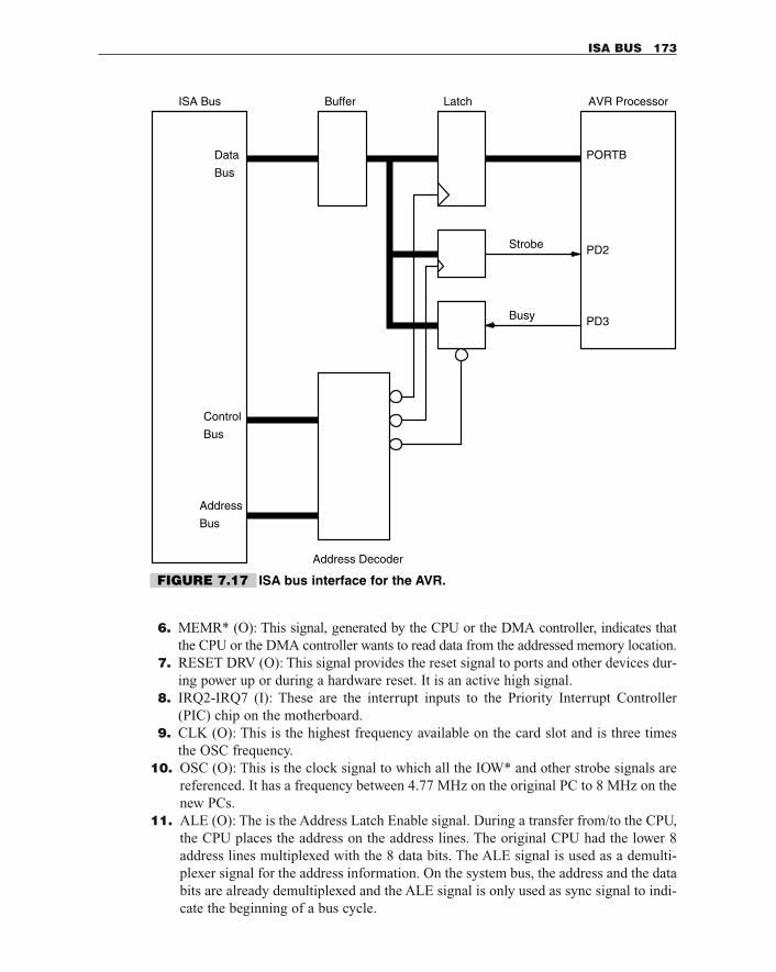
6. MEMR* (O): This signal, generated by the CPU or the DMA controller, indicates thatthe CPU or the DMA controller wants to read data from the addressed memory location.
7. RESET DRV (O): This signal provides the reset signal to ports and other devices dur-ing power up or during a hardware reset. It is an active high signal.
8. IRQ2-IRQ7 (I): These are the interrupt inputs to the Priority Interrupt Controller(PIC) chip on the motherboard.
9. CLK (O): This is the highest frequency available on the card slot and is three timesthe OSC frequency.
10. OSC (O): This is the clock signal to which all the IOW* and other strobe signals arereferenced. It has a frequency between 4.77 MHz on the original PC to 8 MHz on thenew PCs.
11. ALE (O): The is the Address Latch Enable signal. During a transfer from/to the CPU,the CPU places the address on the address lines. The original CPU had the lower 8address lines multiplexed with the 8 data bits. The ALE signal is used as a demulti-plexer signal for the address information. On the system bus, the address and the databits are already demultiplexed and the ALE signal is only used as sync signal to indi-cate the beginning of a bus cycle.
ISA BUS 173
Data
Bus
AVR Processor
PORTB
Buffer
Address Decoder
Address
Bus
Bus
Control
Strobe
Busy
LatchISA Bus
PD2
PD3
FIGURE 7.17 ISA bus interface for the AVR.
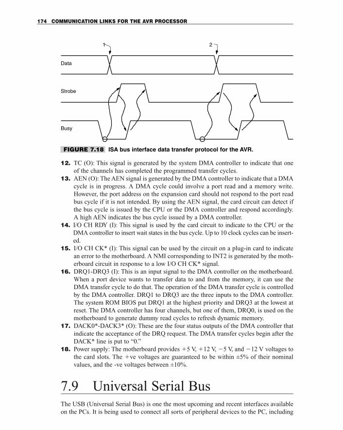
12. TC (O): This signal is generated by the system DMA controller to indicate that oneof the channels has completed the programmed transfer cycles.
13. AEN (O): The AEN signal is generated by the DMA controller to indicate that a DMAcycle is in progress. A DMA cycle could involve a port read and a memory write.However, the port address on the expansion card should not respond to the port readbus cycle if it is not intended. By using the AEN signal, the card circuit can detect ifthe bus cycle is issued by the CPU or the DMA controller and respond accordingly.A high AEN indicates the bus cycle issued by a DMA controller.
14. I/O CH RDY (I): This signal is used by the card circuit to indicate to the CPU or theDMA controller to insert wait states in the bus cycle. Up to 10 clock cycles can be insert-ed.
15. I/O CH CK* (I): This signal can be used by the circuit on a plug-in card to indicatean error to the motherboard. A NMI corresponding to INT2 is generated by the moth-erboard circuit in response to a low I/O CH CK* signal.
16. DRQ1-DRQ3 (I): This is an input signal to the DMA controller on the motherboard.When a port device wants to transfer data to and from the memory, it can use theDMA transfer cycle to do that. The operation of the DMA transfer cycle is controlledby the DMA controller. DRQ1 to DRQ3 are the three inputs to the DMA controller.The system ROM BIOS put DRQ1 at the highest priority and DRQ3 at the lowest atreset. The DMA controller has four channels, but one of them, DRQ0, is used on themotherboard to generate dummy read cycles to refresh dynamic memory.
17. DACK0*-DACK3* (O): These are the four status outputs of the DMA controller thatindicate the acceptance of the DRQ request. The DMA transfer cycles begin after theDACK* line is put to “0.”
18. Power supply: The motherboard provides �5 V, �12 V, �5 V, and �12 V voltages tothe card slots. The �ve voltages are guaranteed to be within ±5% of their nominalvalues, and the -ve voltages between ±10%.
7.9 Universal Serial BusThe USB (Universal Serial Bus) is one the most upcoming and recent interfaces availableon the PCs. It is being used to connect all sorts of peripheral devices to the PC, including
174 COMMUNICATION LINKS FOR THE AVR PROCESSOR
Strobe
Busy
Data
1 2
FIGURE 7.18 ISA bus interface data transfer protocol for the AVR.
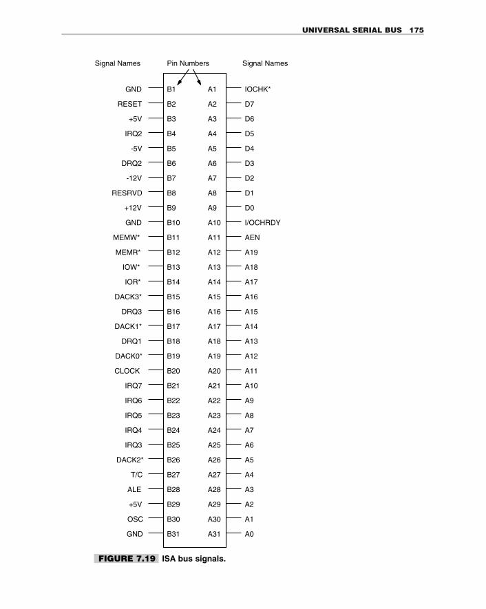
UNIVERSAL SERIAL BUS 175
Signal Names
A1
A2
A3
A4
A5
A6
A7
A8
A9
A10
A11
A12
A13
A14
A15
A16
A17
A18
A19
A20
A21
A22
A23
A24
A25
A26
A27
A28
A29
A30
A31
B1
B2
B3
B4
B5
B6
B7
B8
B9
B10
B11
B12
B13
B14
B15
B16
B17
B18
B19
B20
B21
B22
B23
B24
B25
B26
B27
B28
B29
B30
B31
IOCHK*
D7
D6
D5
D4
D3
D2
D1
D0
I/OCHRDY
AEN
A19
A18
A17
A16
A15
A14
A13
A12
A11
A10
A9
A8
A7
A6
A5
A4
A3
A2
A1
A0
Pin NumbersSignal Names
GND
RESET
+5V
IRQ2
-5V
DRQ2
-12V
RESRVD
+12V
GND
MEMW*
MEMR*
IOW*
IOR*
DACK3*
DRQ3
DACK1*
DRQ1
DACK0*
CLOCK
IRQ7
IRQ6
IRQ5
IRQ4
IRQ3
DACK2*
T/C
ALE
+5V
OSC
GND
FIGURE 7.19 ISA bus signals.
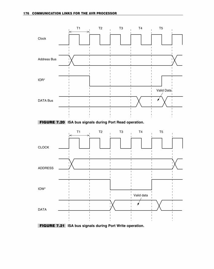
176 COMMUNICATION LINKS FOR THE AVR PROCESSOR
DATA Bus
IOR*
Address Bus
Clock
Valid Data
T1 T2 T3 T4 T5
DATA
IOW*
ADDRESS
CLOCK
Valid data
T1 T2 T3 T4 T5
FIGURE 7.20 ISA bus signals during Port Read operation.
FIGURE 7.21 ISA bus signals during Port Write operation.
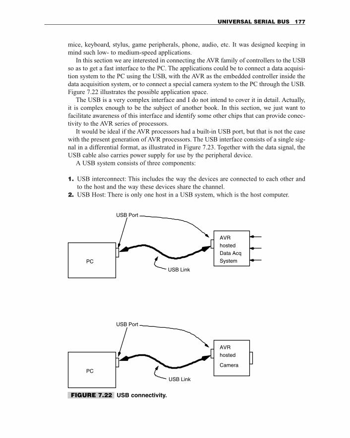
mice, keyboard, stylus, game peripherals, phone, audio, etc. It was designed keeping inmind such low- to medium-speed applications.
In this section we are interested in connecting the AVR family of controllers to the USBso as to get a fast interface to the PC. The applications could be to connect a data acquisi-tion system to the PC using the USB, with the AVR as the embedded controller inside thedata acquisition system, or to connect a special camera system to the PC through the USB.Figure 7.22 illustrates the possible application space.
The USB is a very complex interface and I do not intend to cover it in detail. Actually,it is complex enough to be the subject of another book. In this section, we just want tofacilitate awareness of this interface and identify some other chips that can provide conec-tivity to the AVR series of processors.
It would be ideal if the AVR processors had a built-in USB port, but that is not the casewith the present generation of AVR processors. The USB interface consists of a single sig-nal in a differential format, as illustrated in Figure 7.23. Together with the data signal, theUSB cable also carries power supply for use by the peripheral device.
A USB system consists of three components:
1. USB interconnect: This includes the way the devices are connected to each other andto the host and the way these devices share the channel.
2. USB Host: There is only one host in a USB system, which is the host computer.
UNIVERSAL SERIAL BUS 177
USB Link
AVR
hosted
USB Port
USB Link
AVR
hosted
Data Acq
System
USB Port
PC
PC
Camera
FIGURE 7.22 USB connectivity.
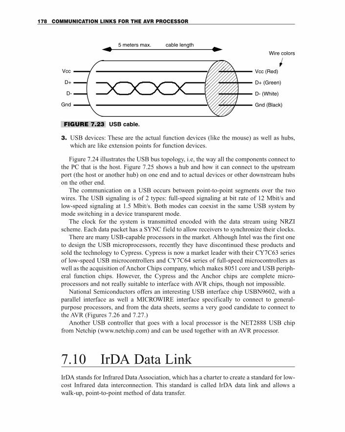
3. USB devices: These are the actual function devices (like the mouse) as well as hubs,which are like extension points for function devices.
Figure 7.24 illustrates the USB bus topology, i.e, the way all the components connect tothe PC that is the host. Figure 7.25 shows a hub and how it can connect to the upstreamport (the host or another hub) on one end and to actual devices or other downstream hubson the other end.
The communication on a USB occurs between point-to-point segments over the twowires. The USB signaling is of 2 types: full-speed signaling at bit rate of 12 Mbit/s andlow-speed signaling at 1.5 Mbit/s. Both modes can coexist in the same USB system bymode switching in a device transparent mode.
The clock for the system is transmitted encoded with the data stream using NRZIscheme. Each data packet has a SYNC field to allow receivers to synchronize their clocks.
There are many USB-capable processors in the market. Although Intel was the first oneto design the USB microprocessors, recently they have discontinued these products andsold the technology to Cypress. Cypress is now a market leader with their CY7C63 seriesof low-speed USB microcontrollers and CY7C64 series of full-speed microcontrollers aswell as the acquisition of Anchor Chips company, which makes 8051 core and USB periph-eral function chips. However, the Cypress and the Anchor chips are complete micro-processors and not really suitable to interface with AVR chips, though not impossible.
National Semiconductors offers an interesting USB interface chip USBN9602, with aparallel interface as well a MICROWIRE interface specifically to connect to general-purpose processors, and from the data sheets, seems a very good candidate to connect tothe AVR (Figures 7.26 and 7.27.)
Another USB controller that goes with a local processor is the NET2888 USB chipfrom Netchip (www.netchip.com) and can be used together with an AVR processor.
7.10 IrDA Data LinkIrDA stands for Infrared Data Association, which has a charter to create a standard for low-cost Infrared data interconnection. This standard is called IrDA data link and allows awalk-up, point-to-point method of data transfer.
178 COMMUNICATION LINKS FOR THE AVR PROCESSOR
���
����
���
Vcc
D+
D-
Gnd
5 meters max. cable length
Vcc (Red)
D+ (Green)
D- (White)
Gnd (Black)
Wire colors
FIGURE 7.23 USB cable.
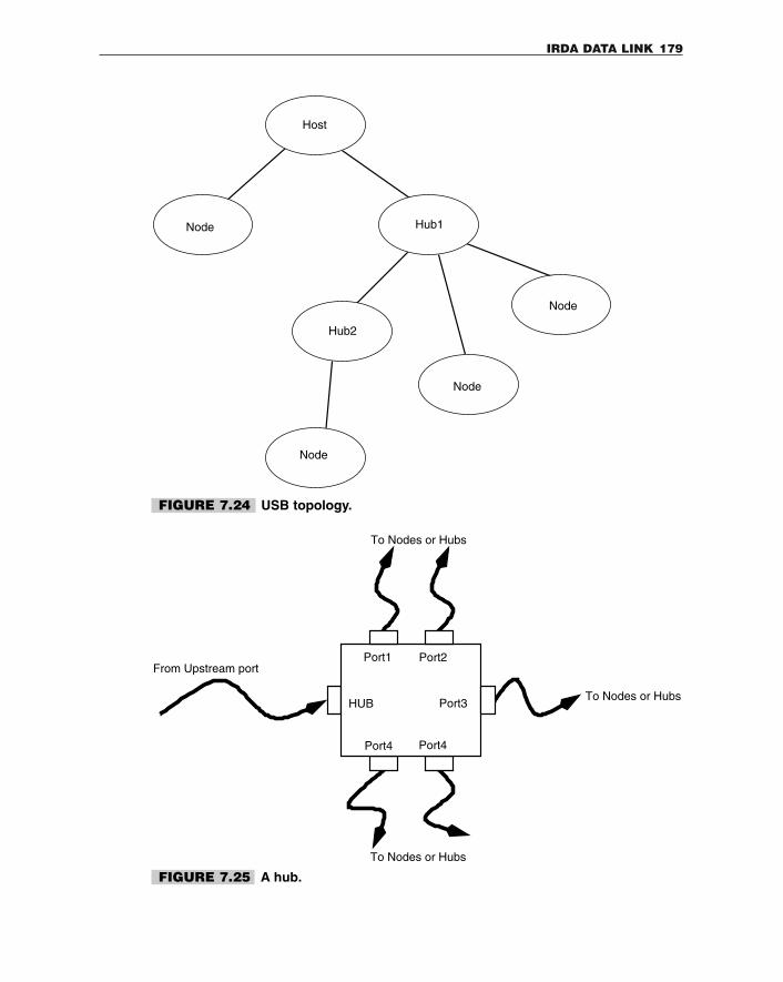
IRDA DATA LINK 179
Host
Hub1
Hub2
Node
Node
Node
Node
FIGURE 7.24 USB topology.
From Upstream port
To Nodes or Hubs
To Nodes or Hubs
To Nodes or Hubs
Port1 Port2
Port3
Port4Port4
HUB
FIGURE 7.25 A hub.
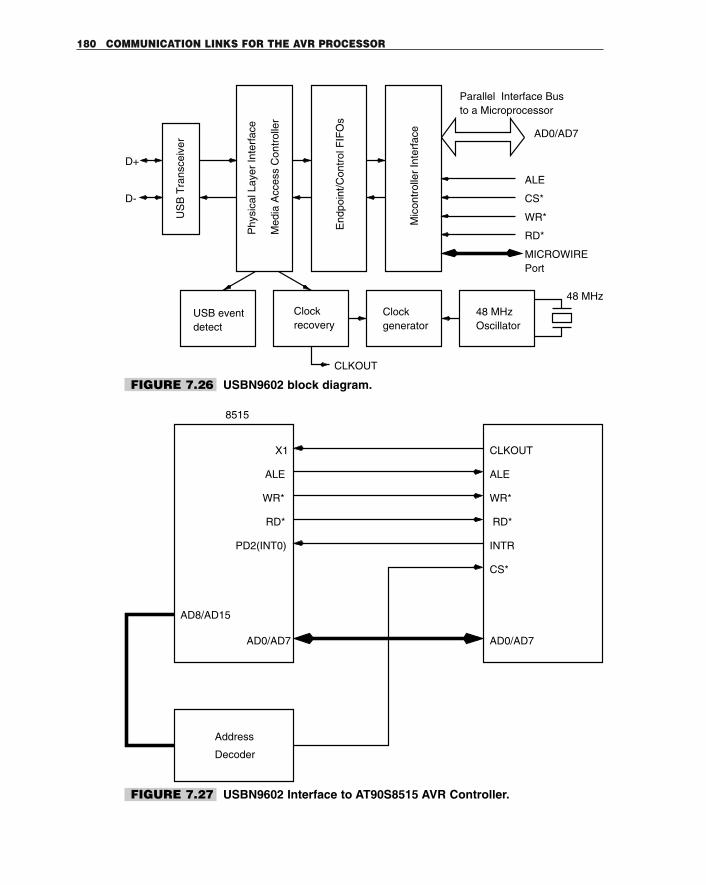
180 COMMUNICATION LINKS FOR THE AVR PROCESSOR
Mic
ontr
olle
r In
terf
ace
USB eventdetect
Clockrecovery
Clock generator
48 MHzOscillator
End
poin
t/Con
trol
FIF
Os
Phy
sica
l Lay
er In
terf
ace
Med
ia A
cces
s C
ontr
olle
r
US
B T
rans
ceiv
er
D+
D-
CLKOUT
48 MHz
Parallel Interface Busto a Microprocessor
AD0/AD7
ALE
CS*
RD*
WR*
MICROWIREPort
FIGURE 7.26 USBN9602 block diagram.
8515
CLKOUT
ALE
WR*
RD*
INTR
AD0/AD7AD0/AD7
PD2(INT0)
X1
ALE
WR*
RD*
AD8/AD15
CS*
Address
Decoder
FIGURE 7.27 USBN9602 Interface to AT90S8515 AVR Controller.
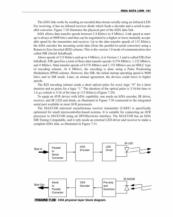
The IrDA link works by sending an encoded data stream serially using an infrared LED.For receiving, it has an infrared receiver diode which feeds a decoder and a serial-to-par-allel converter. Figure 7.28 illustrates the physical part of the IrDA data link.
IrDA allows data transfer speeds between 2.4 Kbits/s to 4 Mbits/s. Link speed at start-up is always at 9600 bits/s and then can be negotiated to a higher or lower mutually accept-able speed by the transmitter and receiver. Up to the data transfer speeds of 115 Kbits/s,the IrDA encodes the incoming serial data (from the parallel-to-serial converter) using aReturn to Zero Inverted (RZI) scheme. This is the version 1.0 mode of communication alsocalled SIR (Serial InfraRead).
Above speeds of 115 Kbits/s and up to 4 Mbits/s, it is Version 1.1 and is called FIR (FastInfraRed). FIR specifies a total of three data transfer speeds: 0.576 Mbits/s, 1.152 Mbits/s,and 4 Mbits/s. Data transfer speeds of 0.576 Mbits/s and 1.152 Mbits/s use an HDLC typeof encoding scheme. At 4 Mbits/s, the encoding is done using a Pulse PositioningModulation (PPM) scheme. However, like SIR, the initial startup operating speed is 9600bits/s and in SIR mode. Later, on mutual agreement, the devices could move to higherspeeds.
The RZI encoding scheme sends a short optical pulse for every logic “0” for a shortduration and no pulse for a logic “1.” The duration of the optical pulse is 3/16-bit time or1.6 �s (which is 3/16 of bit time at 115 Kbits/s) (Figure 7.29).
To equip an AVR device with IrDA capability, one needs an IrDA encoder, IR driver,receiver, and IR LED and diode, as illustrated in Figure 7.30 connected to the integratedserial port available in most AVR processors.
The MAX3100 universal asynchronous receiver transmitter (UART) is specificallyoptimized for small microcontroller-based systems. It is suitable for connecting an AVRprocessor to MAX3100 using an SPI/Microwire interface. The MAX3100 has an IrDASIR Timing Compatable, and it only needs an external LED driver and receiver to make acomplete IrDA link, as illustrated in Figure 7.31.
IRDA DATA LINK 181
IR LED
IR DIODE
ParalleltoSerialConverter
Serialto
ConverterParallel
IrDAEncoder
IrDADecoder
LEDDriver
Pre-ampandQuantizer
Byte In
Byte Out
FIGURE 7.28 IrDA physical layer block diagram.
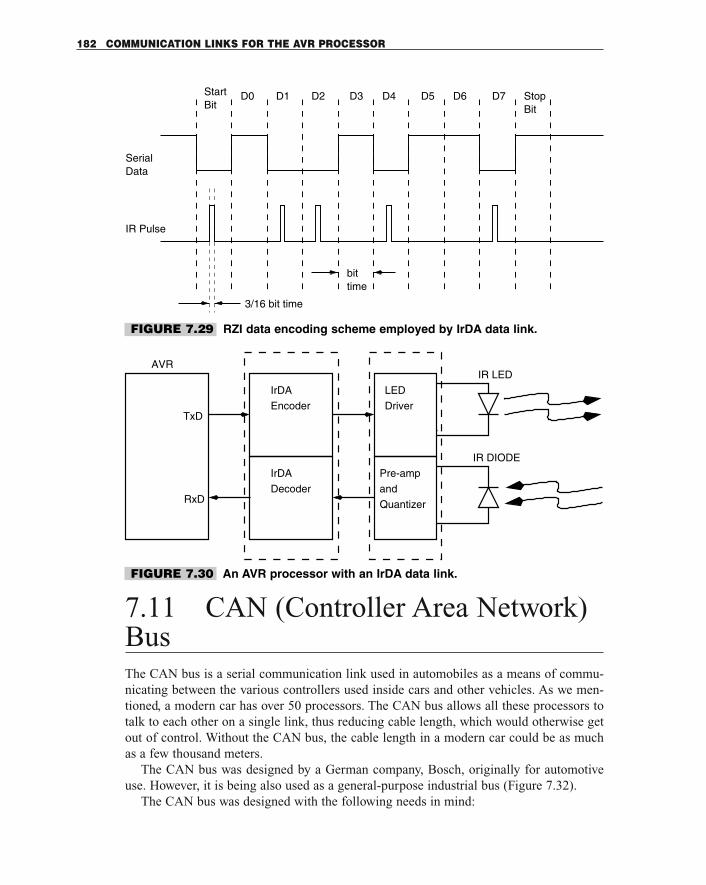
7.11 CAN (Controller Area Network)BusThe CAN bus is a serial communication link used in automobiles as a means of commu-nicating between the various controllers used inside cars and other vehicles. As we men-tioned, a modern car has over 50 processors. The CAN bus allows all these processors totalk to each other on a single link, thus reducing cable length, which would otherwise getout of control. Without the CAN bus, the cable length in a modern car could be as muchas a few thousand meters.
The CAN bus was designed by a German company, Bosch, originally for automotiveuse. However, it is being also used as a general-purpose industrial bus (Figure 7.32).
The CAN bus was designed with the following needs in mind:
182 COMMUNICATION LINKS FOR THE AVR PROCESSOR
StartBit
D0 D1 D2 D3 D4 D5 D6 D7 Stop
IR Pulse
Data
3/16 bit time
bittime
Serial
Bit
FIGURE 7.29 RZI data encoding scheme employed by IrDA data link.
IR LED
IrDA
Encoder
LED
Driver
IR DIODE
IrDA
Decoder
Pre-amp
and
Quantizer
TxD
RxD
AVR
FIGURE 7.30 An AVR processor with an IrDA data link.
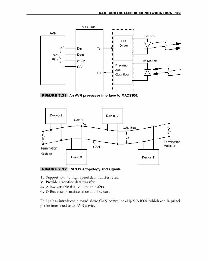
1. Support low- to high-speed data transfer rates.2. Provide error-free data transfer.3. Allow variable data volume transfers.4. Offers ease of maintenance and low cost.
Philips has introduced a stand-alone CAN controller chip SJA1000, which can in princi-ple be interfaced to an AVR device.
CAN (CONTROLLER AREA NETWORK) BUS 183
IR LED
LED
Driver
IR DIODE
Pre-amp
and
Quantizer
AVR
Din
Dout
SCLK
CS*
MAX3100
Port
Pins
Tx
Rx
FIGURE 7.31 An AVR processor interface to MAX3100.
Device 1 Device 2
Device 3 Device 4
CAN Bus
CANH
CANL
Vd
Termination
Resistor
Termination Resistor
FIGURE 7.32 CAN bus topology and signals.

This page intentionally left blank.
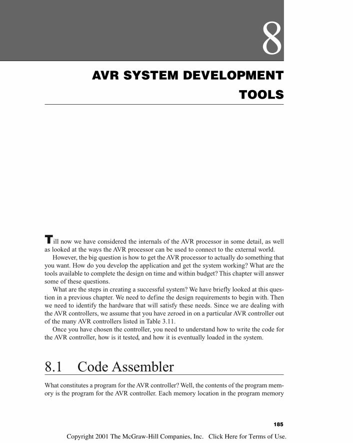
Till now we have considered the internals of the AVR processor in some detail, as wellas looked at the ways the AVR processor can be used to connect to the external world.
However, the big question is how to get the AVR processor to actually do something thatyou want. How do you develop the application and get the system working? What are thetools available to complete the design on time and within budget? This chapter will answersome of these questions.
What are the steps in creating a successful system? We have briefly looked at this ques-tion in a previous chapter. We need to define the design requirements to begin with. Thenwe need to identify the hardware that will satisfy these needs. Since we are dealing withthe AVR controllers, we assume that you have zeroed in on a particular AVR controller outof the many AVR controllers listed in Table 3.11.
Once you have chosen the controller, you need to understand how to write the code forthe AVR controller, how is it tested, and how it is eventually loaded in the system.
8.1 Code AssemblerWhat constitutes a program for the AVR controller? Well, the contents of the program mem-ory is the program for the AVR controller. Each memory location in the program memory
8AVR SYSTEM DEVELOPMENT
TOOLS
185
Copyright 2001 The McGraw-Hill Companies, Inc. Click Here for Terms of Use.
map of the AVR controller is a 16-bit word. This 16-bit word constitutes the op-code andthe (optional) operand. The controller reads the program memory and interprets the binaryword. For human convenience, rather than handle the op-codes, you can use the mnemonicrepresentation of the op-codes (e.g., CLI, Clear Global Interrupt flag, is a mnemonic repre-sentation of the op-code: $94F0). However, the controller understands the op-code and notthe mnemonic, and so you need a translation program that takes the mnemonic codes andtranslates these codes into op-codes. The program that does this job is called an assembler.
An assembler takes a text file called the source file, with the mnemonic representationof the program (simply called the source code) and converts it into another file with themachine op-codes (simply called the machine code or object code).
8.1.1 AVR FAMILY ASSEMBLER
One of the assemblers available for AVR controllers is from Atmel. It is called avrasm andcan be downloaded from the atmel site. The assembler covers the entire range of AVR con-trollers (Figure 8.1).
The assembler takes an assembler source code file and translates it into an object codefile. The object code can be used as an input to a simulator or an emulator. The assembleralso generates a file containing the code that can be programmed into the chip by a suit-able programmer. The avrasm is a very simple assembler and takes only a single inputassembler code file. It is not possible to link other object code files using the avrasm.
The avrasm can also generate an EEPROM file if EEPROM data has been allocated inthe assembler source file.
186 AVR SYSTEM DEVELOPMENT TOOLS
FIGURE 8.1 Windows version of the AVR Assembler.
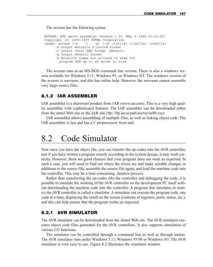
The avrasm has the following syntax.
AVRASM: AVR macro assembler version 1.21 (Mar 5 1998 01:21:00)Copyright (C) 1995-1997 ATMEL Corporationusage: avrasm [-m -i -g] [-w] <infile> <lisfile> <romfile>
-m Output Motorola S-record format-i Output Intel HEX format (default)-g Output Generic format-w Relative jumps are allowed to wrap for
program ROM up to 4k words in size
The avrasm runs as an MS-DOS command line version. There is also a windows ver-sion available for Windows 3.11, Windows 95, or Windows NT. The windows version ofthe avrasm is wavrasm, and this has online help. However, the wavrasm cannot assemblevery large source files.
8.1.2 IAR ASSEMBLER
IAR assembler is a shareware product from IAR (www.iar.com). This is a very high qual-ity assembler with sophisticated features. The IAR assembler can be downloaded eitherfrom the atmel Web site or the IAR site (ftp://ftp.iar.se/pub/mirror/aa90.exe).
IAR assembler allows assembling of multiple files, as well as linking object code. TheIAR assembler is fast and has a C preprocessor front end.
8.2 Code SimulatorNow once you have the object file, you can transfer the op-codes into the AVR controller,and if you have written a program exactly according to the system design, it may work cor-rectly. However, there are good chances that your program does not work as expected. Insuch a case, you will need to find out where the errors are and make suitable changes oradditions to the source file, assemble the source file again, and load the machine code intothe controller. This may be a time-consuming, iterative process.
Rather than transferring the op-codes into the controller and debugging the code, it ispossible to simulate the working of the AVR controller on the development PC itself with-out downloading the machine code into the controller. A program that simulates or mim-ics the AVR controller is called a simulator. A simulator can execute the program code, onecode at a time, displaying the result on the screen (contents of registers, ports, status, etc.),and this can help ensure that the program works as expected.
8.2.1 AVR SIMULATOR
The AVR simulator can be downloaded from the Atmel Web site. The AVR simulator exe-cutes object code files generated for the AVR controllers. It also supports simulation ofvarious I/O functions.
The simulator can be controlled through a command line as well as through menus.The AVR simulator runs under Windows 3.11, Windows 95/98 or Windows NT. The AVRsimulator is very easy to use. Figure 8.2 illustrates the simulator window.
CODE SIMULATOR 187
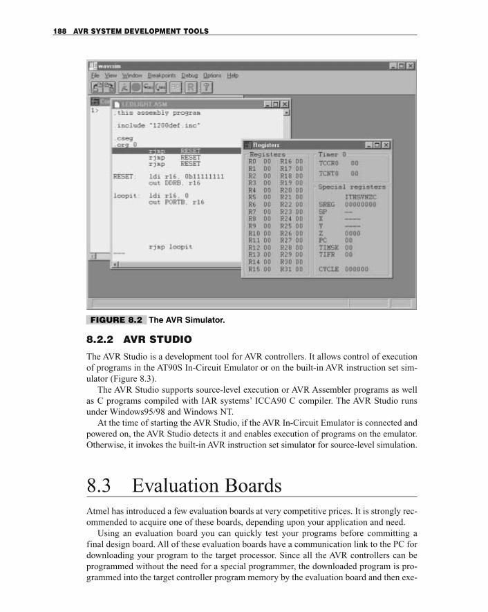
8.2.2 AVR STUDIO
The AVR Studio is a development tool for AVR controllers. It allows control of executionof programs in the AT90S In-Circuit Emulator or on the built-in AVR instruction set sim-ulator (Figure 8.3).
The AVR Studio supports source-level execution or AVR Assembler programs as wellas C programs compiled with IAR systems’ ICCA90 C compiler. The AVR Studio runsunder Windows95/98 and Windows NT.
At the time of starting the AVR Studio, if the AVR In-Circuit Emulator is connected andpowered on, the AVR Studio detects it and enables execution of programs on the emulator.Otherwise, it invokes the built-in AVR instruction set simulator for source-level simulation.
8.3 Evaluation BoardsAtmel has introduced a few evaluation boards at very competitive prices. It is strongly rec-ommended to acquire one of these boards, depending upon your application and need.
Using an evaluation board you can quickly test your programs before committing afinal design board. All of these evaluation boards have a communication link to the PC fordownloading your program to the target processor. Since all the AVR controllers can beprogrammed without the need for a special programmer, the downloaded program is pro-grammed into the target controller program memory by the evaluation board and then exe-
188 AVR SYSTEM DEVELOPMENT TOOLS
FIGURE 8.2 The AVR Simulator.
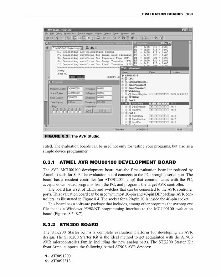
cuted. The evaluation boards can be used not only for testing your programs, but also as asimple device programmer.
8.3.1 ATMEL AVR MCU00100 DEVELOPMENT BOARD
The AVR MCU00100 development board was the first evaluation board introduced byAtmel. It sells for $49. The evaluation board connects to the PC through a serial port. Theboard has a resident controller (an AT89C2051 chip) that communicates with the PC,accepts downloaded programs from the PC, and programs the target AVR controller.
The board has a set of LEDs and switches that can be connected to the AVR controllerports. This evaluation board can be used with most 20-pin and 40-pin DIP package AVR con-trollers, as illustrated in Figure 8.4. The socket for a 20-pin IC is inside the 40-pin socket.
This board has a software package that includes, among other programs the avrprog.exefile that is a Windows 95/98/NT programming interface to the MCU00100 evaluationboard (Figures 8.5–8.7).
8.3.2 STK200 BOARD
The STK200 Starter Kit is a complete evaluation platform for developing an AVRdesign. The STK200 Starter Kit is the ideal method to get acquainted with the AT90SAVR microcontroller family, including the new analog parts. The STK200 Starter Kitfrom Atmel supports the following Atmel AT90S AVR devices:
1. AT90S12002. AT90S2313
EVALUATION BOARDS 189
FIGURE 8.3 The AVR Studio.
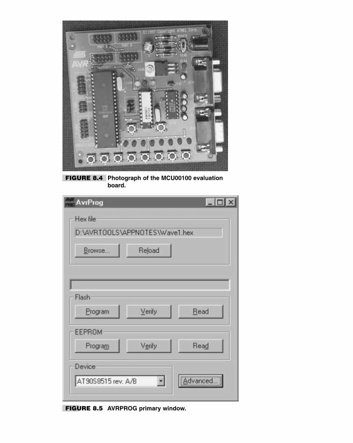
FIGURE 8.4 Photograph of the MCU00100 evaluation board.
FIGURE 8.5 AVRPROG primary window.
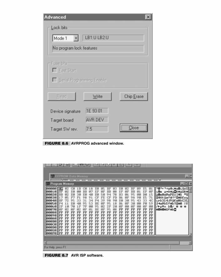
FIGURE 8.7 AVR ISP software.
FIGURE 8.6 AVRPROG advanced window.
3. AT90S23234. AT90LS23235. AT90S23436. AT90LS23437. AT90S23338. AT90LS23339. AT90S4414
10. AT90S443311. AT90LS443312. AT90S851513. AT90S853514. AT90LS8535
The STK200 development board is complete with push-button switches and LEDs. Allof the microcontroller ports are accessible through 0.1-inch headers on the board. The reg-ulated power supply accepts a DC or AC input voltage source, and 3.3-V or 5-V operationcan be selected by jumper settings. The on-board brownout detector circuit is user selec-table to 2.9 V or 4.5 V.
An external LCD can be interfaced to the AVR microcontroller via a standard 14-pinheader on the board. A potentiometer is supplied for contrast adjustment. The STK200 hassupport for external SRAM with sockets for Address latch and SRAM device. The inter-nal 10-bit A/D converter on the analog AVR microcontroller is accessible through a sepa-rate header connector on the edge of the board. The analog reference voltage can be adjust-ed with an on-board potentiometer or optionally with an external reference voltage.
The STK200 board includes an In-System Programming (ISP) cable that connects theSTK200 board to the PC through the PC parallel port. The ISP cable can also be used toprogram all classic Atmel AVR microcontrollers in the actual target application via a 10-pin header. Figure 8.8 is a photograph of the STK200 evaluation board.
Support site from Atmel: AVR 8-Bit RISC Support Tools http://www.atmel.com/atmel/products/prod202.htm
STK200 Starter Kit Manual (40 pages, updated 2/99): http://www.atmel.com/atmel/acrobat/doc1107.pdf
8.3.3 STK 300 BOARD
If you are planning to use any of the AVR mega devices, then you need the STK300 board.It is very similar to the STK200 but only supports ATmega603, ATmega603L,ATmega103m, and ATmega103L.
8.4 ICE200 AVR EmulatorAtmel has recently introduced a low-cost In-Circuit Emulator, the ICE200, priced at $200.An In-Circuit Emulator has a pod that is connected to the target controller socket during
192 AVR SYSTEM DEVELOPMENT TOOLS
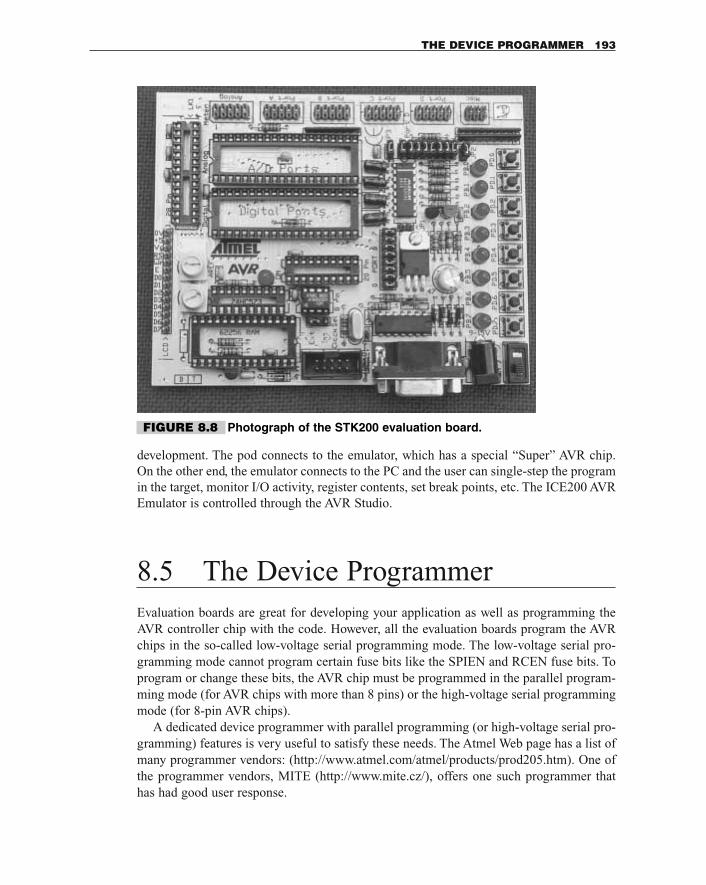
development. The pod connects to the emulator, which has a special “Super” AVR chip.On the other end, the emulator connects to the PC and the user can single-step the programin the target, monitor I/O activity, register contents, set break points, etc. The ICE200 AVREmulator is controlled through the AVR Studio.
8.5 The Device ProgrammerEvaluation boards are great for developing your application as well as programming theAVR controller chip with the code. However, all the evaluation boards program the AVRchips in the so-called low-voltage serial programming mode. The low-voltage serial pro-gramming mode cannot program certain fuse bits like the SPIEN and RCEN fuse bits. Toprogram or change these bits, the AVR chip must be programmed in the parallel program-ming mode (for AVR chips with more than 8 pins) or the high-voltage serial programmingmode (for 8-pin AVR chips).
A dedicated device programmer with parallel programming (or high-voltage serial pro-gramming) features is very useful to satisfy these needs. The Atmel Web page has a list ofmany programmer vendors: (http://www.atmel.com/atmel/products/prod205.htm). One ofthe programmer vendors, MITE (http://www.mite.cz/), offers one such programmer thathas had good user response.
THE DEVICE PROGRAMMER 193
FIGURE 8.8 Photograph of the STK200 evaluation board.
8.6 AVR System Design withComponents off the Shelf (COTS)8.6.1 The SimmStick magic
SimmStick™ is a 30-pin simm-socket-based Single Board Computer designed by AnttiLukats from Estonia, originally for the PIC16Cxx chips. The simm socket used is the com-mon 30-pin one used for many years on PC motherboards.
SimStick is now available for Atmel AVR processors for both 20- and 40-pin DIP pack-aging. The SimmStick system consists of a motherboard (the backplane). The motherboard(such as DT003) has space for up to four daughtercards such as the DT103/104 controllercard, additional daughtercards such as DT201 (one-inch prototype board), DT202 (two-inch prototype board), DT203 (LEDs, switches, ULN2803 drivers board) or the DT205(relay board for four relays).
PIN # NAME DESCRIPTION
1 A1 Special IO
2 A2 Special IO
3 A3 Special IO or Negative Supply
4 PWR Unregulated DC in or �12V or VPP
5 CI Clock Input or OSC1
6 CO Clock Output or OSC2
7 VDD �5 V In or Out
8 RES Reset In or Out
9 GND Digital Ground
10 SCL I2C Clock or I/O
11 SDA I2C Data or I/O
12 SI Serial In or I/O
13 SO Serial Out or I/O
14 IO General-purpose I/O
15 D0 General I/O
16 D1 General I/O
17 D2 General I/O
18 D3 General I/O
19 D4 General I/O
20 D5 General I/O
21 D6 General I/O
22 D7 General I/O
194 AVR SYSTEM DEVELOPMENT TOOLS
SimmStick Bus Pinout
23 D8 General I/O
24 D9 General I/O
25 D10 General I/O
26 D11 General I/O
27 D12 General I/O
28 D13 General I/O
29 D14 General I/O
30 D15 General I/O
The advantage of adopting the SimmStick approach is the great speed of system devel-opment. It is claimed (and rightly so) that a simple working AT90S1200 application can bewired on the DT104 board in under five minutes.
Figure 8.9 illustrates the DT104 circuit schematic, Figure 8.10 illustrates the DT104PCB component overlay, and Figure 8.11 illustrates a populated DT104 photograph.
More details about the SimmStick boards are available at www.dontronics.com.
8.7 Code Development with a High-Level LanguageFor larger AVR processors, using a high-level language for developing your applicationwould be very useful and convenient. Currently, high-level language compilers for C aswell as Basic are available. For the C language, IAR’s C compiler (www.iar.com) is report-ed to be the best and also the most expensive. Many inexpensive or free compilers areavailable, and some of these are listed below.
8.7.1 C-AVR: A C COMPILER FOR AVR
C-AVR is a low-cost C compiler that I have used to develop code for the dual-channel volt-meter project in this book. The features of this compiler are:
1. Supports all members of the AVR family which have stack. e.g. 2313, 2323, 4414,8515, 8535, etc., and ATmega603/103. (Also available is a low-cost version, C-AVR-N, which has the same features but does not support mega devices.)
2. Uses (and includes) Atmel’s AVRASM assembler, so output of the compiler can bedebugged with Atmel’s AVR Studio debugger.
3. Supported data types: char, unsigned char, int, unsigned int, long int, unsigned long int, float.4. Runs off Windows 95/98.5. Includes Visual Code Generator (VCG). Using the VCG, on-chip peripheral functions
(such as a serial port) can be visually programmed. E.g., you may just enter the crystalfrequency and the desired baud rate; the VCG generates C language statements such as“UBRR � 0x18” and “UCR � 0x20,” etc.
CODE DEVELOPMENT WITH A HIGH-LEVEL LANGUAGE 195
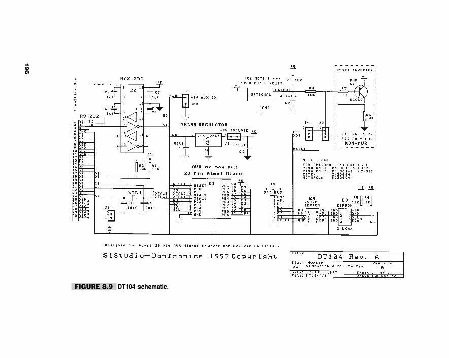
FIGURE 8.9 DT104 schematic.
19
6
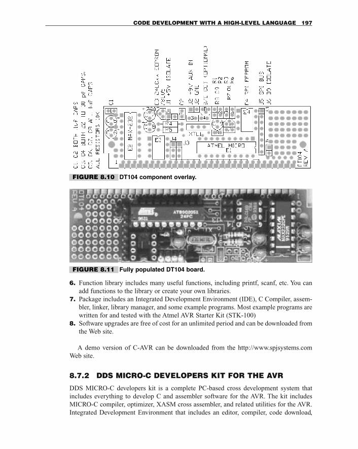
6. Function library includes many useful functions, including printf, scanf, etc. You canadd functions to the library or create your own libraries.
7. Package includes an Integrated Development Environment (IDE), C Compiler, assem-bler, linker, library manager, and some example programs. Most example programs arewritten for and tested with the Atmel AVR Starter Kit (STK-100)
8. Software upgrades are free of cost for an unlimited period and can be downloaded fromthe Web site.
A demo version of C-AVR can be downloaded from the http://www.spjsystems.comWeb site.
8.7.2 DDS MICRO-C DEVELOPERS KIT FOR THE AVR
DDS MICRO-C developers kit is a complete PC-based cross development system thatincludes everything to develop C and assembler software for the AVR. The kit includesMICRO-C compiler, optimizer, XASM cross assembler, and related utilities for the AVR.Integrated Development Environment that includes an editor, compiler, code download,
CODE DEVELOPMENT WITH A HIGH-LEVEL LANGUAGE 197
FIGURE 8.10 DT104 component overlay.
FIGURE 8.11 Fully populated DT104 board.
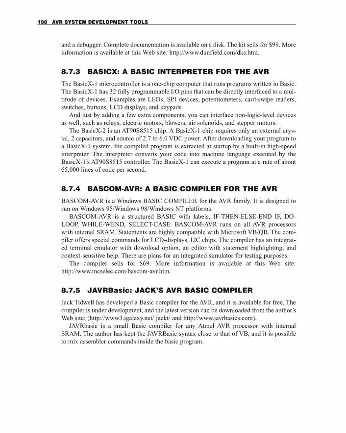
and a debugger. Complete documentation is available on a disk. The kit sells for $99. Moreinformation is available at this Web site: http://www.dunfield.com/dks.htm.
8.7.3 BASICX: A BASIC INTERPRETER FOR THE AVR
The BasicX-1 microcontroller is a one-chip computer that runs programs written in Basic.The BasicX-1 has 32 fully programmable I/O pins that can be directly interfaced to a mul-titude of devices. Examples are LEDs, SPI devices, potentiometers, card-swipe readers,switches, buttons, LCD displays, and keypads.
And just by adding a few extra components, you can interface non-logic-level devicesas well, such as relays, electric motors, blowers, air solenoids, and stepper motors.
The BasicX-2 is an AT90S8515 chip. A BasicX-1 chip requires only an external crys-tal, 2 capacitors, and source of 2.7 to 6.0 VDC power. After downloading your program toa BasicX-1 system, the compiled program is extracted at startup by a built-in high-speedinterpreter. The interpreter converts your code into machine language executed by theBasicX-1’s AT90S8515 controller. The BasicX-1 can execute a program at a rate of about65,000 lines of code per second.
8.7.4 BASCOM-AVR: A BASIC COMPILER FOR THE AVR
BASCOM-AVR is a Windows BASIC COMPILER for the AVR family. It is designed torun on Windows 95/Windows 98/Windows NT platforms.
BASCOM-AVR is a structured BASIC with labels, IF-THEN-ELSE-END IF, DO-LOOP, WHILE-WEND, SELECT-CASE. BASCOM-AVR runs on all AVR processorswith internal SRAM. Statements are highly compatible with Microsoft VB/QB. The com-piler offers special commands for LCD-displays, I2C chips. The compiler has an integrat-ed terminal emulator with download option, an editor with statement highlighting, andcontext-sensitive help. There are plans for an integrated simulator for testing purposes.
The compiler sells for $69. More information is available at this Web site:http://www.mcselec.com/bascom-avr.htm.
8.7.5 JAVRBasic: JACK’S AVR BASIC COMPILER
Jack Tidwell has developed a Basic compiler for the AVR, and it is available for free. Thecompiler is under development, and the latest version can be downloaded from the author’sWeb site: (http://www3.igalaxy.net/ jackt/ and http://www.javrbasics.com).
JAVRbasic is a small Basic compiler for any Atmel AVR processor with internalSRAM. The author has kept the JAVRBasic syntax close to that of VB, and it is possibleto mix assembler commands inside the basic program.
198 AVR SYSTEM DEVELOPMENT TOOLS

If you are like most people, eventually you would like to build your system. The usualsteps in completely designing a system is to put your ideas on a piece of paper, estimatethe required hardware, draw some flow chart of the software, simulate the design on anyavailable tool, and then finalize the design. Eventually it will come to a stage where youmust build it and test it. For those who earn a living from electronic design, you must alsothink of production plans for your design.
At this point, we will consider various options that are popularly used to prototype elec-tronic circuits and systems. I have put together a list of tools that I have found useful inprototyping my projects. I also offer some suggestions on some soldering tools for variousapplications.
9.1 Why Prototype?An important questions could be raised at this stage. Why prototype the design at all? Whatdoes prototyping the design gain you? After all, you may have to make the PCB for thedesign anyway? Why not go directly for the final PCB?
Prototyping allows you to test your design and evaluate its performance at a very littlecost and rapidly. If you have gone through the process of making a PCB, you will realize
9PROTOTYPING TECHNIQUES
199
Copyright 2001 The McGraw-Hill Companies, Inc. Click Here for Terms of Use.
that this time-consuming process of capture, board layout, and fabrication will delay thecrucial task of verifying your design. Besides, the design itself may be in a preliminarystage and you may want to add and modify the design and see the performance on a protoboard. So prototyping your design is a good idea. For hobbyists, the prototype could be thefinal design anyway.
The importance of design verification while still on the drawing board (or the designboard—whatever) cannot be overemphasized. It is a good idea to thoroughly check thedesign while it is still on the paper. Another way to check your design is to simulate the performance of the complete or part of the circuit design on any simulation tool that isavailable, say a code simulator. However, the prototyping stage of the design will give youone last opportunity to check that the performance is according to specifications and isbulletproof, and hopefully you will be saved the embarrassment of a failed and returnedproduct from the field or from the customer.
There is a possible downside to prototyping as well. Many times there is an urge to rushyour circuit and see it working as a prototype without giving it much thought while it is inthe design stage. It is advisable to control this urge and to prototype the idea when you aresatisfied that the design has been well-thought out and suitably simulated. A badlydesigned circuit that has been rushed to the proto stage could end up in an endless andvicious loop of modify-prototype-test. This must be avoided at all costs.
9.2 OK, So You Want to PrototypeThere are many ways of prototyping your circuit. For very simple circuits, it is popular touse the protoboard. The protoboard is made of plastic (or some such material) with holesat a 0.1-inch pitch in the form of a regular matrix. The holes in a given row are internallyconnected. The holes are of a certain diameter that accepts most component leads such assmall diodes, resistors, transistors, and ICs in DIP packages, etc. On either side of the pro-toboard, there are two columns of connected holes that are usually used as a power bus toconnect the protoboard to a DC voltage source for energizing the circuit. Figure 9.1 is aphotograph of a popular protoboard.
To use the protoboard, one simply pushes the components in the holes and makesrequired connections with suitable single-strand hookup wire. The protoboard is a simpleand convenient way to test your circuit. And it does not require you to dirty your handswith the soldering rod. However, the protoboard is not suitable for high-speed applications.The inductive coupling between the rows of connections may produce unwanted and unde-sirable crosstalk.
Another simple method is to use the commonly available general-purpose board madeof glass epoxy, the material that the PCB is usually made of. This board, usually referredto as a “sea of holes,” is available in many formats form many suppliers. Figure 9.2 is aphotograph of a general-purpose PCB. This general-purpose circuit board has holesarranged on a 0.1-inch pitch with solder contacts on one side. These boards are also avail-able with many connector pinouts as well, to connect to say a DB-25 connector.Prototyping boards for the PC interface connectors are also available.
200 PROTOTYPING TECHNIQUES
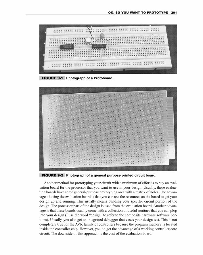
Another method for prototyping your circuit with a minimum of effort is to buy an eval-uation board for the processor that you want to use in your design. Usually, these evalua-tion boards have some general-purpose prototyping area with a matrix of holes. The advan-tage of using the evaluation board is that you can use the resources on the board to get yourdesign up and running. This usually means building your specific circuit portion of thedesign. The processor part of the design is used from the evaluation board. Another advan-tage is that these boards usually come with a collection of useful routines that you can plopinto your design (I use the word “design” to refer to the composite hardware software por-tions). Usually, you also get an integrated debugger that eases your design test. This is notcompletely true for the AVR family of controllers because the program memory is locatedinside the controller chip. However, you do get the advantage of a working controller corecircuit. The downside of this approach is the cost of the evaluation board.
OK, SO YOU WANT TO PROTOTYPE 201
FIGURE 9-1 Photograph of a Protoboard.
FIGURE 9-2 Photograph of a general purpose printed circuit board.
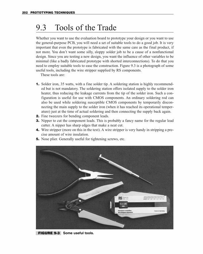
9.3 Tools of the TradeWhether you want to use the evaluation board to prototype your design or you want to usethe general-purpose PCB, you will need a set of suitable tools to do a good job. It is veryimportant that even the prototype is fabricated with the same care as the final product, ifnot more. You don’t want some silly, sloppy solder job to be a cause of a nonfunctionaldesign. Since you are testing a new design, you want the influence of other variables to beminimal (like a badly fabricated prototype with shorted interconnections). To do that youneed to employ suitable tools to ease the construction. Figure 9.3 is a photograph of someuseful tools, including the wire stripper supplied by RS components.
These tools are:
1. Solder iron, 35 watts, with a fine solder tip. A soldering station is highly recommend-ed but is not mandatory. The soldering station offers isolated supply to the solder ironheater, thus reducing the leakage currents from the tip of the solder iron. Such a con-figuration is useful for use with CMOS components. An ordinary soldering rod canalso be used while soldering susceptible CMOS components by temporarily discon-necting the main supply to the solder iron (when it has reached its operational temper-ature) just at the time of actual soldering and then connecting the supply back again.
2. Fine tweezers for bending component leads.3. Nipper to cut the component leads. This is probably a fancy name for the regular lead
cutter. A nipper has sharp edges that make a neat cut.4. Wire stripper (more on this in the text). A wire stripper is very handy in stripping a pre-
cise amount of wire insulation.5. Nose plier. Generally useful for tightening screws, etc.
202 PROTOTYPING TECHNIQUES
FIGURE 9-3 Some useful tools.
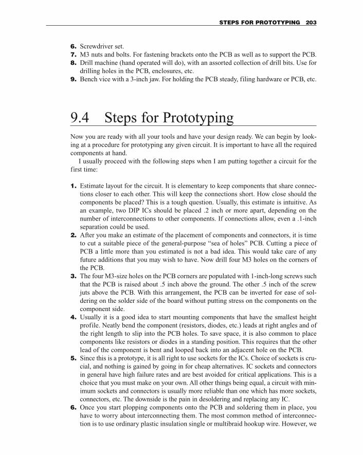
6. Screwdriver set.7. M3 nuts and bolts. For fastening brackets onto the PCB as well as to support the PCB.8. Drill machine (hand operated will do), with an assorted collection of drill bits. Use for
drilling holes in the PCB, enclosures, etc.9. Bench vice with a 3-inch jaw. For holding the PCB steady, filing hardware or PCB, etc.
9.4 Steps for PrototypingNow you are ready with all your tools and have your design ready. We can begin by look-ing at a procedure for prototyping any given circuit. It is important to have all the requiredcomponents at hand.
I usually proceed with the following steps when I am putting together a circuit for thefirst time:
1. Estimate layout for the circuit. It is elementary to keep components that share connec-tions closer to each other. This will keep the connections short. How close should thecomponents be placed? This is a tough question. Usually, this estimate is intuitive. Asan example, two DIP ICs should be placed .2 inch or more apart, depending on thenumber of interconnections to other components. If connections allow, even a .1-inchseparation could be used.
2. After you make an estimate of the placement of components and connectors, it is timeto cut a suitable piece of the general-purpose “sea of holes” PCB. Cutting a piece ofPCB a little more than you estimated is not a bad idea. This would take care of anyfuture additions that you may wish to have. Now drill four M3 holes on the corners ofthe PCB.
3. The four M3-size holes on the PCB corners are populated with 1-inch-long screws suchthat the PCB is raised about .5 inch above the ground. The other .5 inch of the screwjuts above the PCB. With this arrangement, the PCB can be inverted for ease of sol-dering on the solder side of the board without putting stress on the components on thecomponent side.
4. Usually it is a good idea to start mounting components that have the smallest heightprofile. Neatly bend the component (resistors, diodes, etc.) leads at right angles and ofthe right length to slip into the PCB holes. To save space, it is also common to placecomponents like resistors or diodes in a standing position. This requires that the otherlead of the component is bent and looped back into an adjacent hole on the PCB.
5. Since this is a prototype, it is all right to use sockets for the ICs. Choice of sockets is cru-cial, and nothing is gained by going in for cheap alternatives. IC sockets and connectorsin general have high failure rates and are best avoided for critical applications. This is achoice that you must make on your own. All other things being equal, a circuit with min-imum sockets and connectors is usually more reliable than one which has more sockets,connectors, etc. The downside is the pain in desoldering and replacing any IC.
6. Once you start plopping components onto the PCB and soldering them in place, youhave to worry about interconnecting them. The most common method of interconnec-tion is to use ordinary plastic insulation single or multibraid hookup wire. However, we
STEPS FOR PROTOTYPING 203
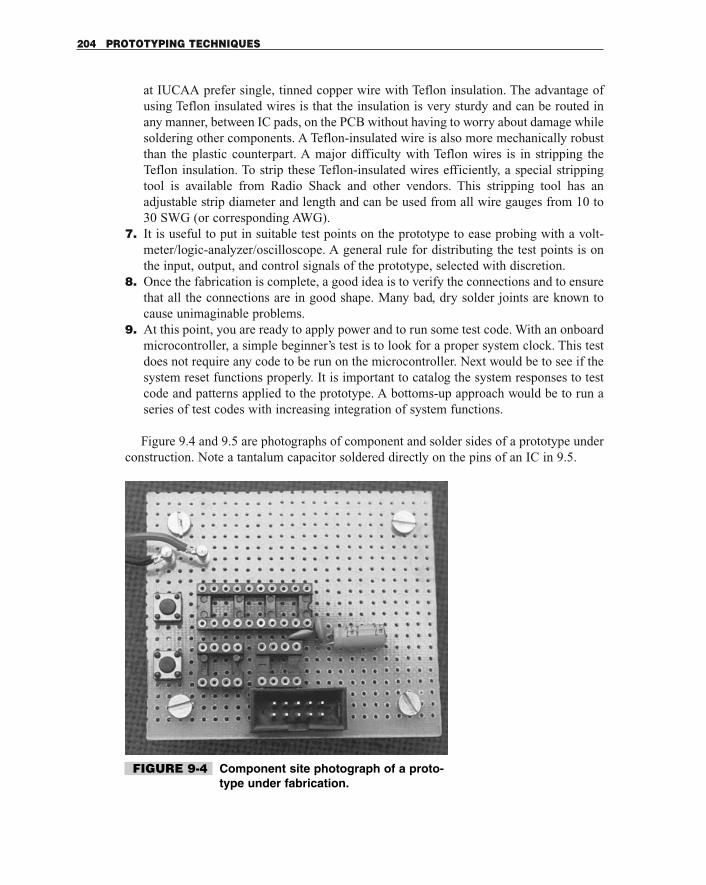
at IUCAA prefer single, tinned copper wire with Teflon insulation. The advantage ofusing Teflon insulated wires is that the insulation is very sturdy and can be routed inany manner, between IC pads, on the PCB without having to worry about damage whilesoldering other components. A Teflon-insulated wire is also more mechanically robustthan the plastic counterpart. A major difficulty with Teflon wires is in stripping theTeflon insulation. To strip these Teflon-insulated wires efficiently, a special strippingtool is available from Radio Shack and other vendors. This stripping tool has anadjustable strip diameter and length and can be used from all wire gauges from 10 to30 SWG (or corresponding AWG).
7. It is useful to put in suitable test points on the prototype to ease probing with a volt-meter/logic-analyzer/oscilloscope. A general rule for distributing the test points is onthe input, output, and control signals of the prototype, selected with discretion.
8. Once the fabrication is complete, a good idea is to verify the connections and to ensurethat all the connections are in good shape. Many bad, dry solder joints are known tocause unimaginable problems.
9. At this point, you are ready to apply power and to run some test code. With an onboardmicrocontroller, a simple beginner’s test is to look for a proper system clock. This testdoes not require any code to be run on the microcontroller. Next would be to see if thesystem reset functions properly. It is important to catalog the system responses to testcode and patterns applied to the prototype. A bottoms-up approach would be to run aseries of test codes with increasing integration of system functions.
Figure 9.4 and 9.5 are photographs of component and solder sides of a prototype underconstruction. Note a tantalum capacitor soldered directly on the pins of an IC in 9.5.
204 PROTOTYPING TECHNIQUES
FIGURE 9-4 Component site photograph of a proto-type under fabrication.
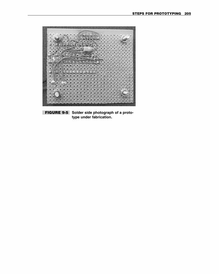
STEPS FOR PROTOTYPING 205
FIGURE 9-5 Solder side photograph of a proto-type under fabrication.

This page intentionally left blank.
10.1 At a GlanceSalient features of this chapter are:
An elementary project that you can build in a couple of hours.
Uses an AT90S1200 and sundry components.
Discusses alternative designs.
Shows how to write code in a variety of ways.
Shows how to modify the circuit and code for an 8-pin AT90S2343.
10.2 IntroductionWith this chapter, we begin the last section of the book, that of projects. I will illustrate thevarious features of the Atmel AVR RISC controllers with a series of practical applicationsthat can be used right away or can be used in a larger project.
10AVR PROJECT 1
SMART DICE: A DICE WITH AN ATTITUDE
207
Copyright 2001 The McGraw-Hill Companies, Inc. Click Here for Terms of Use.
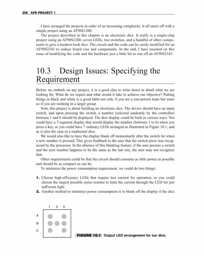
I have arranged the projects in order of an increasing complexity. It all starts off with asimple project using an AT90S1200.
The project described in this chapter is an electronic dice. It really is a single-chipproject using an AT90S1200, seven LEDs, two switches, and a handful of other compo-nents to give a modern-look dice. The circuit and the code can be easily modified for anAT90S2343 to reduce board size and components. In the end, I have touched on thisissue of modifying the code and the hardware just a little bit to run off an AT90S2343.
10.3 Design Issues: Specifying theRequirementBefore we embark on any project, it is a good idea to write down in detail what we arelooking for. What do we expect and what would it take to achieve our objective? Puttingthings in black and white is a good habit not only if you are a one-person team but moreso if you are working in a larger group.
Now, this project is about building an electronic dice. The device should have an inputswitch, and upon pressing the switch, a number (selected randomly by the controller)between 1 and 6 should be displayed. The dice display could be built in various ways. Youcould have a 7-segment display that would display the number (between 1 to 6) when youpress a key, or you could have 7 ordinary LEDs arranged as illustrated in Figure 10.1, andas is also the case in a traditional dice.
We would also like to have the display blank off momentarily after the switch for whena new number is pressed. This gives feedback to the user that the switch press was recog-nized by the processor. In the absence of this blanking feature, if the user presses a switchand the next number happens to be the same as the last one, the user may not recognizethat.
Other requirements could be that the circuit should consume as little power as possibleand should be as compact as can be.
To minimize the power consumption requirement, we could do two things:
1. Choose high-efficiency LEDs that require less current for operation, or you couldchoose the largest possible series resistor to limit the current through the LED for justsufficient light.
2. Another method to minimize power consumption is to blank off the display if the dice
208 AVR PROJECT 1
A
B
C
1 2 3
FIGURE 10.1 Output LED arrangement for our dice.
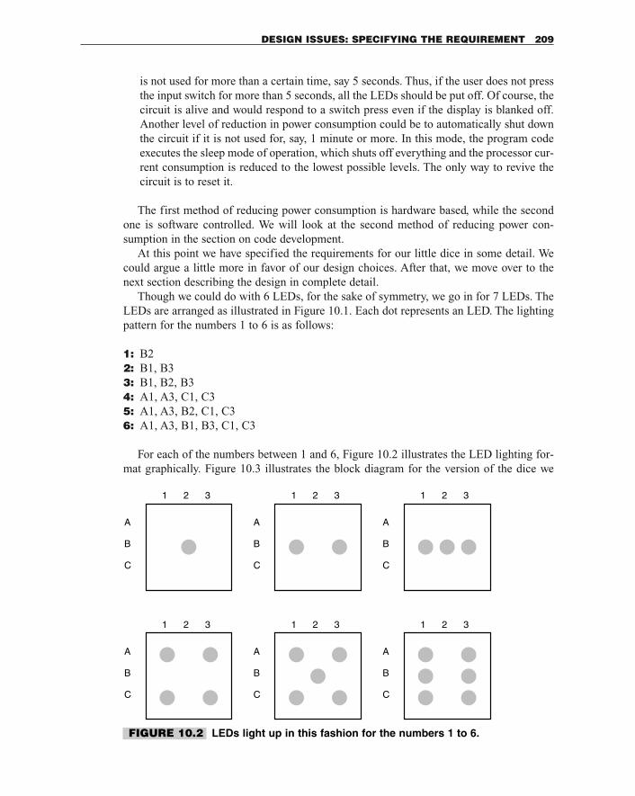
is not used for more than a certain time, say 5 seconds. Thus, if the user does not pressthe input switch for more than 5 seconds, all the LEDs should be put off. Of course, thecircuit is alive and would respond to a switch press even if the display is blanked off.Another level of reduction in power consumption could be to automatically shut downthe circuit if it is not used for, say, 1 minute or more. In this mode, the program codeexecutes the sleep mode of operation, which shuts off everything and the processor cur-rent consumption is reduced to the lowest possible levels. The only way to revive thecircuit is to reset it.
The first method of reducing power consumption is hardware based, while the secondone is software controlled. We will look at the second method of reducing power con-sumption in the section on code development.
At this point we have specified the requirements for our little dice in some detail. Wecould argue a little more in favor of our design choices. After that, we move over to thenext section describing the design in complete detail.
Though we could do with 6 LEDs, for the sake of symmetry, we go in for 7 LEDs. TheLEDs are arranged as illustrated in Figure 10.1. Each dot represents an LED. The lightingpattern for the numbers 1 to 6 is as follows:
1: B22: B1, B33: B1, B2, B34: A1, A3, C1, C35: A1, A3, B2, C1, C36: A1, A3, B1, B3, C1, C3
For each of the numbers between 1 and 6, Figure 10.2 illustrates the LED lighting for-mat graphically. Figure 10.3 illustrates the block diagram for the version of the dice we
DESIGN ISSUES: SPECIFYING THE REQUIREMENT 209
A
B
C
1 2 3
A
B
C
1 2 3
A
B
C
1 2 3
A
B
C
1 2 3
A
B
C
1 2 3
A
B
C
1 2 3
FIGURE 10.2 LEDs light up in this fashion for the numbers 1 to 6.
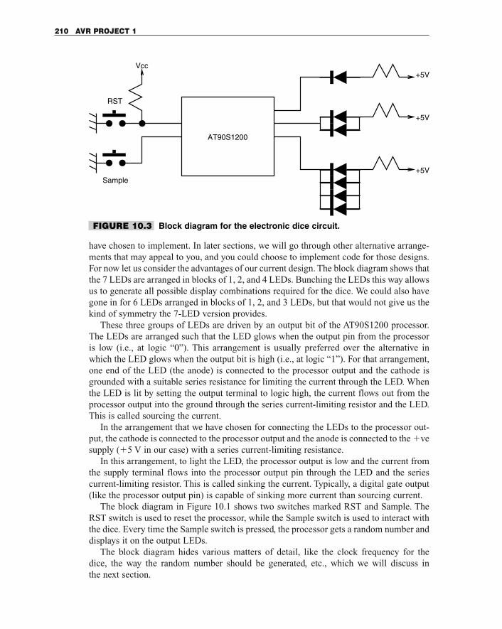
have chosen to implement. In later sections, we will go through other alternative arrange-ments that may appeal to you, and you could choose to implement code for those designs.For now let us consider the advantages of our current design. The block diagram shows thatthe 7 LEDs are arranged in blocks of 1, 2, and 4 LEDs. Bunching the LEDs this way allowsus to generate all possible display combinations required for the dice. We could also havegone in for 6 LEDs arranged in blocks of 1, 2, and 3 LEDs, but that would not give us thekind of symmetry the 7-LED version provides.
These three groups of LEDs are driven by an output bit of the AT90S1200 processor.The LEDs are arranged such that the LED glows when the output pin from the processoris low (i.e., at logic “0”). This arrangement is usually preferred over the alternative inwhich the LED glows when the output bit is high (i.e., at logic “1”). For that arrangement,one end of the LED (the anode) is connected to the processor output and the cathode isgrounded with a suitable series resistance for limiting the current through the LED. Whenthe LED is lit by setting the output terminal to logic high, the current flows out from theprocessor output into the ground through the series current-limiting resistor and the LED.This is called sourcing the current.
In the arrangement that we have chosen for connecting the LEDs to the processor out-put, the cathode is connected to the processor output and the anode is connected to the �vesupply (�5 V in our case) with a series current-limiting resistance.
In this arrangement, to light the LED, the processor output is low and the current fromthe supply terminal flows into the processor output pin through the LED and the series current-limiting resistor. This is called sinking the current. Typically, a digital gate output(like the processor output pin) is capable of sinking more current than sourcing current.
The block diagram in Figure 10.1 shows two switches marked RST and Sample. TheRST switch is used to reset the processor, while the Sample switch is used to interact withthe dice. Every time the Sample switch is pressed, the processor gets a random number anddisplays it on the output LEDs.
The block diagram hides various matters of detail, like the clock frequency for the dice, the way the random number should be generated, etc., which we will discuss in the next section.
210 AVR PROJECT 1
Vcc
AT90S1200
RST
Sample
+5V
+5V
+5V
FIGURE 10.3 Block diagram for the electronic dice circuit.
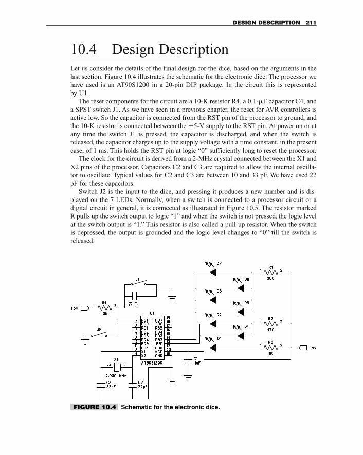
10.4 Design DescriptionLet us consider the details of the final design for the dice, based on the arguments in thelast section. Figure 10.4 illustrates the schematic for the electronic dice. The processor wehave used is an AT90S1200 in a 20-pin DIP package. In the circuit this is represented by U1.
The reset components for the circuit are a 10-K resistor R4, a 0.1-�F capacitor C4, anda SPST switch J1. As we have seen in a previous chapter, the reset for AVR controllers isactive low. So the capacitor is connected from the RST pin of the processor to ground, andthe 10-K resistor is connected between the �5-V supply to the RST pin. At power on or atany time the switch J1 is pressed, the capacitor is discharged, and when the switch isreleased, the capacitor charges up to the supply voltage with a time constant, in the presentcase, of 1 ms. This holds the RST pin at logic “0” sufficiently long to reset the processor.
The clock for the circuit is derived from a 2-MHz crystal connected between the X1 andX2 pins of the processor. Capacitors C2 and C3 are required to allow the internal oscilla-tor to oscillate. Typical values for C2 and C3 are between 10 and 33 pF. We have used 22pF for these capacitors.
Switch J2 is the input to the dice, and pressing it produces a new number and is dis-played on the 7 LEDs. Normally, when a switch is connected to a processor circuit or adigital circuit in general, it is connected as illustrated in Figure 10.5. The resistor markedR pulls up the switch output to logic “1” and when the switch is not pressed, the logic levelat the switch output is “1.” This resistor is also called a pull-up resistor. When the switchis depressed, the output is grounded and the logic level changes to “0” till the switch isreleased.
DESIGN DESCRIPTION 211
FIGURE 10.4 Schematic for the electronic dice.
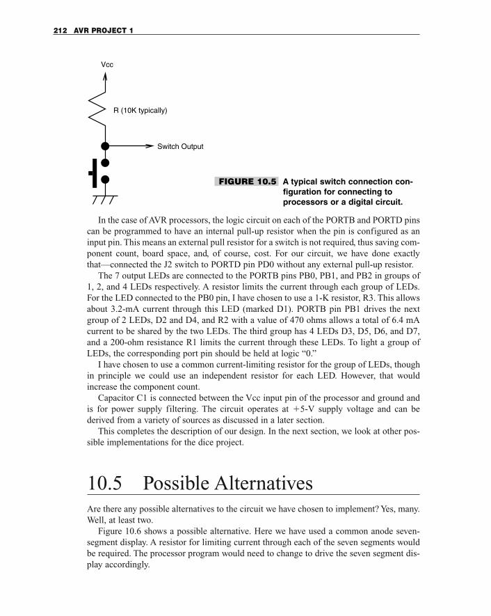
In the case of AVR processors, the logic circuit on each of the PORTB and PORTD pinscan be programmed to have an internal pull-up resistor when the pin is configured as aninput pin. This means an external pull resistor for a switch is not required, thus saving com-ponent count, board space, and, of course, cost. For our circuit, we have done exactlythat—connected the J2 switch to PORTD pin PD0 without any external pull-up resistor.
The 7 output LEDs are connected to the PORTB pins PB0, PB1, and PB2 in groups of1, 2, and 4 LEDs respectively. A resistor limits the current through each group of LEDs.For the LED connected to the PB0 pin, I have chosen to use a 1-K resistor, R3. This allowsabout 3.2-mA current through this LED (marked D1). PORTB pin PB1 drives the nextgroup of 2 LEDs, D2 and D4, and R2 with a value of 470 ohms allows a total of 6.4 mAcurrent to be shared by the two LEDs. The third group has 4 LEDs D3, D5, D6, and D7,and a 200-ohm resistance R1 limits the current through these LEDs. To light a group ofLEDs, the corresponding port pin should be held at logic “0.”
I have chosen to use a common current-limiting resistor for the group of LEDs, thoughin principle we could use an independent resistor for each LED. However, that wouldincrease the component count.
Capacitor C1 is connected between the Vcc input pin of the processor and ground andis for power supply filtering. The circuit operates at �5-V supply voltage and can bederived from a variety of sources as discussed in a later section.
This completes the description of our design. In the next section, we look at other pos-sible implementations for the dice project.
10.5 Possible AlternativesAre there any possible alternatives to the circuit we have chosen to implement? Yes, many.Well, at least two.
Figure 10.6 shows a possible alternative. Here we have used a common anode seven-segment display. A resistor for limiting current through each of the seven segments wouldbe required. The processor program would need to change to drive the seven segment dis-play accordingly.
212 AVR PROJECT 1
Vcc
Switch Output
R (10K typically)
FIGURE 10.5 A typical switch connection con-figuration for connecting toprocessors or a digital circuit.
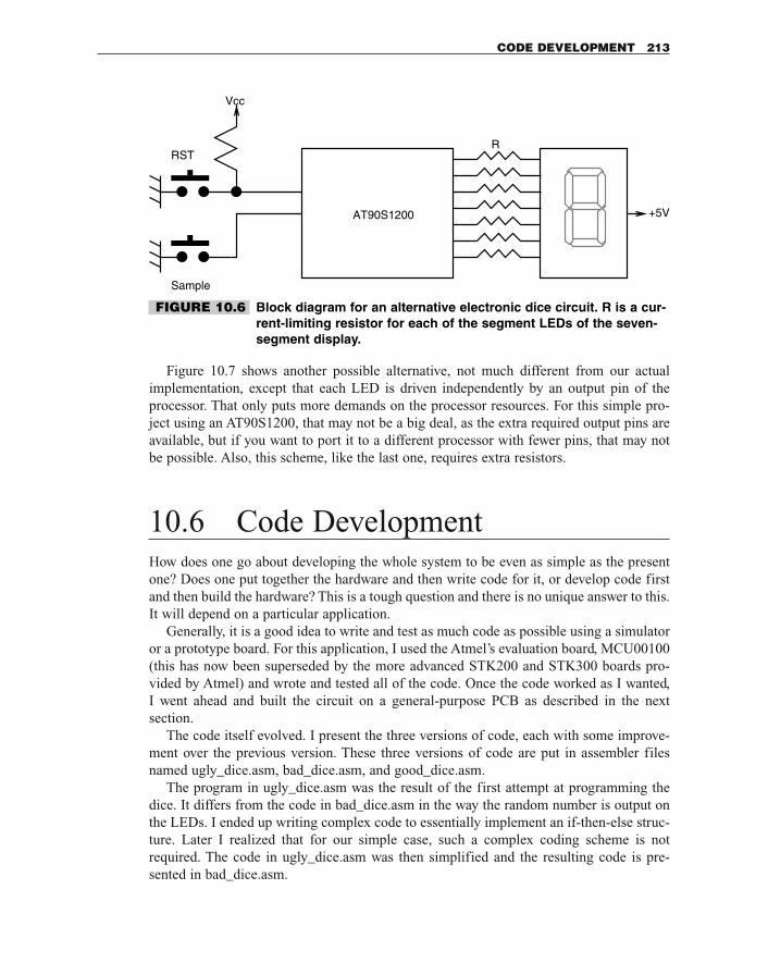
Figure 10.7 shows another possible alternative, not much different from our actualimplementation, except that each LED is driven independently by an output pin of theprocessor. That only puts more demands on the processor resources. For this simple pro-ject using an AT90S1200, that may not be a big deal, as the extra required output pins areavailable, but if you want to port it to a different processor with fewer pins, that may notbe possible. Also, this scheme, like the last one, requires extra resistors.
10.6 Code DevelopmentHow does one go about developing the whole system to be even as simple as the presentone? Does one put together the hardware and then write code for it, or develop code firstand then build the hardware? This is a tough question and there is no unique answer to this.It will depend on a particular application.
Generally, it is a good idea to write and test as much code as possible using a simulatoror a prototype board. For this application, I used the Atmel’s evaluation board, MCU00100(this has now been superseded by the more advanced STK200 and STK300 boards pro-vided by Atmel) and wrote and tested all of the code. Once the code worked as I wanted,I went ahead and built the circuit on a general-purpose PCB as described in the next section.
The code itself evolved. I present the three versions of code, each with some improve-ment over the previous version. These three versions of code are put in assembler filesnamed ugly_dice.asm, bad_dice.asm, and good_dice.asm.
The program in ugly_dice.asm was the result of the first attempt at programming thedice. It differs from the code in bad_dice.asm in the way the random number is output onthe LEDs. I ended up writing complex code to essentially implement an if-then-else struc-ture. Later I realized that for our simple case, such a complex coding scheme is notrequired. The code in ugly_dice.asm was then simplified and the resulting code is pre-sented in bad_dice.asm.
CODE DEVELOPMENT 213
Vcc
RST
Sample
+5V
R
AT90S1200
FIGURE 10.6 Block diagram for an alternative electronic dice circuit. R is a cur-rent-limiting resistor for each of the segment LEDs of the seven-segment display.
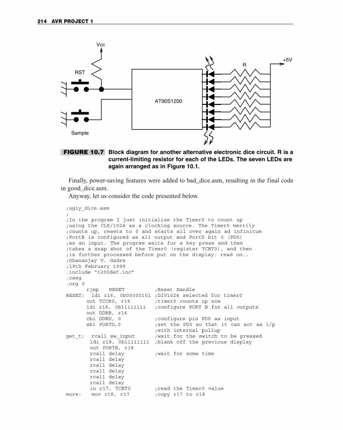
Finally, power-saving features were added to bad_dice.asm, resulting in the final codein good_dice.asm.
Anyway, let us consider the code presented below.
;ugly_dice.asm;;In the program I just initialize the Timer0 to count up;using the CLK/1024 as a clocking source. The Timer0 merrily;counts up, resets to 0 and starts all over again ad infinitum;PortB is configured as all output and PortD bit 0 (PD0);as an input. The program waits for a key press and then;takes a snap shot of the Timer0 (register TCNT0), and then;is further processed before put on the display. read on..;Dhananjay V. Gadre;19th February 1999.include “1200def.inc”.cseg.org 0
rjmp RESET ;Reset HandleRESET: ldi r16, 0b00000101 ;DIV1024 selected for timer0
out TCCR0, r16 ;timer0 counts up nowldi r16, 0b11111111 ;configure PORT B for all outputsout DDRB, r16cbi DDRD, 0 ;configure pin PD0 as inputsbi PORTD,0 ;set the PD0 so that it can act as i/p
;with internal pullupget_t: rcall sw_input ;wait for the switch to be pressed
ldi r18, 0b11111111 ;blank off the previous displayout PORTB, r18rcall delay ;wait for some timercall delayrcall delayrcall delayrcall delayrcall delayin r17, TCNT0 ;read the Timer0 value
more: mov r18, r17 ;copy r17 to r18
214 AVR PROJECT 1
Vcc
RST
Sample
+5VR
AT90S1200
FIGURE 10.7 Block diagram for another alternative electronic dice circuit. R is acurrent-limiting resistor for each of the LEDs. The seven LEDs areagain arranged as in Figure 10.1.
;now check if the number is less than $06compa: cpi r18, $06
brlo enough ;yes, then nothing more;prepare to output it;else
clc ;clear carry for subsbci r18, $06 ;and subtract $06rjmp compa ;do it till the remainder is
;less than $06enough: cpi r18, $00 ; OK, now the number in r18 is
; between 0 and 5;The following piece of code makes this program ugly;The identification of the number and display can be handled;more cleverly as in bad_dice.asm
brne not_0 ;number is not zeroldi r18, 0b11111110 ;number is 0, so display 1 on theout PORTB, r18 ;LEDs, i.e. light up LED B2rjmp get_t
not_0: cpi r18, $01 ;check if the number in r18 is 1brne not_1ldi r18, 0b11111101 ;yes, so light up B1 and B3out PORTB, r18rjmp get_t
not_1: cpi r18, $02 ;check if it is 2brne not_2 ;no it is notldi r18, 0b11111100 ;yes, it is. so light up B1 and B3out PORTB, r18rjmp get_t
not_2: cpi r18, $03brne not_3ldi r18, 0b11111011out PORTB, r18rjmp get_t
not_3: cpi r18, $04brne not_4ldi r18, 0b11111010out PORTB, r18rjmp get_t
not_4: ldi r18, 0b11111001out PORTB, r18rjmp get_t
;Delay subroutine;uses registers r16 and r18;values are set arbitrarilydelay: ldi r16, 0b11111100loophere: ldi r18, 0b10001110decrement: dec r18
brne decrementdec r16brne loophereret
;returns when a key on PD0 is pressed and released;till then it loops waiting for the key presssw_input: in r16, PIND ;input PORTD pin value
andi r16, 0b00000001 ;isolate PD0 statebrne sw_input ;if switch is not pressed, loop backrcall delay ;if pressed, then wait some time to
;ward off the switch bouncespin_0: in r16, PIND ;now check if the switch is released
andi r16, 0b00000001breq pin_0
CODE DEVELOPMENT 215
rcall delayret ;switch is now released..go back
The code in bad_dice.asm is the same as in ugly_dice.asm, except for the part that dis-plays the resulting number (between 0 and 5). This code is as follows:
;code segment from bad_dice.asmenough: ldi r16, $01 ;since the number is between 0 and 5
;add ‘1’ to make it between 1 and 6add r18, r16com r18 ;the output display LEDs are arranged
;as active low, so complement the result-ing;number
ori r18, 0b11111000 ;set the other unused port pins;to an inactive state
out PORTB, r18 ;display it!rjmp get_t ;that it! go get more
The program uses free-running Timer0 to get the randomness. However, it is possibleto use other methods of random number generation; a prominent one is to use LinearFeedback Shift Register (LFSR) as outlined in a previous chapter. The advantage of theLFSR method is that it only requires a seed to arm the LFSR, and then it will churn outrandom numbers.
For this simple case, where the Timer0 is not going to be used for any other task and isalways available, we could use it full time. The Timer0 is clocked at 1/1024 the clock fre-quency, and since the state of the timer is not known to the user, reading it gives a certainrandomness suitable for our purpose.
The program in good_dice.asm builds upon the code in bad_dice.asm by adding aninterrupt subroutine that occurs every time TCNT0 overflows. With a clock input to thecounter of clk/1024, this occurs every 128 ms for a 2.000-MHz clock. The initializationcode in good_dice.asm initializes three registers as low_timer, med_timer, and high_timerto zero. The interrupt subroutine increments these registers each time the timer overflowoccurs.
By looking at the values in med_timer (you can modify the Timer0 ISR so that it pow-ers down after a longer time), the Timer0 ISR determines whether to blank off the displaywith power-down sleep or not.
The Timer0 interrupt subroutine from good_dice.asm is illustrated below.
;Timer0 ISR from good_dice.asm;low_timer, med_timer and high_timer are three registers;that hold elapsed time. These registers are cleared to zero;by main program every time a key is pressed, else their value;builds up and when it exceeds certain value, this ISR powers;down and puts the processor to sleepTimer_int: in save_status, SREG ;save status in reg save_status
cpi med_timer, $01 ;compare med_timer to 01brne skip_it ;is equal then prepare to power
;downldi temp, 255 ;tri-state all outputsout PORTB, temp ;configure all ports as O/Pout PORTD, temp ;and set all values to ‘1’out DDRD, temp
216 AVR PROJECT 1
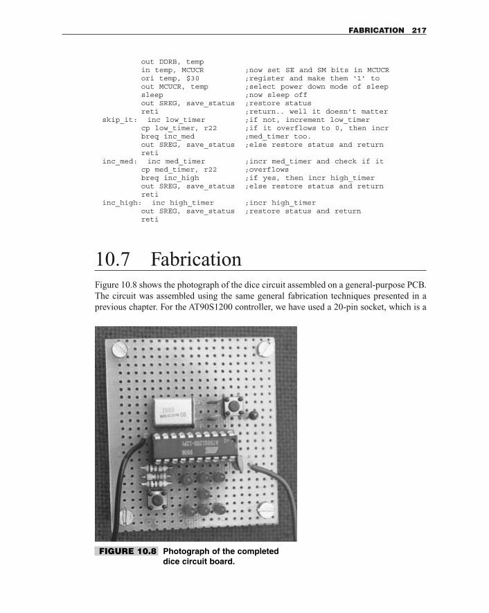
out DDRB, tempin temp, MCUCR ;now set SE and SM bits in MCUCRori temp, $30 ;register and make them ‘1’ toout MCUCR, temp ;select power down mode of sleepsleep ;now sleep offout SREG, save_status ;restore statusreti ;return.. well it doesn’t matter
skip_it: inc low_timer ;if not, increment low_timercp low_timer, r22 ;if it overflows to 0, then incrbreq inc_med ;med_timer too.out SREG, save_status ;else restore status and returnreti
inc_med: inc med_timer ;incr med_timer and check if itcp med_timer, r22 ;overflowsbreq inc_high ;if yes, then incr high_timerout SREG, save_status ;else restore status and returnreti
inc_high: inc high_timer ;incr high_timerout SREG, save_status ;restore status and returnreti
10.7 FabricationFigure 10.8 shows the photograph of the dice circuit assembled on a general-purpose PCB.The circuit was assembled using the same general fabrication techniques presented in aprevious chapter. For the AT90S1200 controller, we have used a 20-pin socket, which is a
FABRICATION 217
FIGURE 10.8 Photograph of the completeddice circuit board.
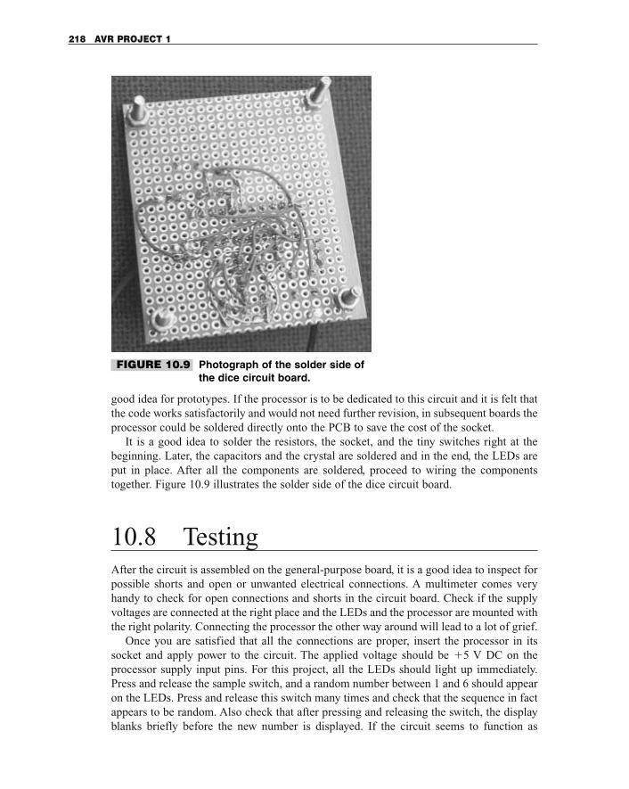
good idea for prototypes. If the processor is to be dedicated to this circuit and it is felt thatthe code works satisfactorily and would not need further revision, in subsequent boards theprocessor could be soldered directly onto the PCB to save the cost of the socket.
It is a good idea to solder the resistors, the socket, and the tiny switches right at thebeginning. Later, the capacitors and the crystal are soldered and in the end, the LEDs areput in place. After all the components are soldered, proceed to wiring the componentstogether. Figure 10.9 illustrates the solder side of the dice circuit board.
10.8 TestingAfter the circuit is assembled on the general-purpose board, it is a good idea to inspect forpossible shorts and open or unwanted electrical connections. A multimeter comes veryhandy to check for open connections and shorts in the circuit board. Check if the supplyvoltages are connected at the right place and the LEDs and the processor are mounted withthe right polarity. Connecting the processor the other way around will lead to a lot of grief.
Once you are satisfied that all the connections are proper, insert the processor in itssocket and apply power to the circuit. The applied voltage should be �5 V DC on theprocessor supply input pins. For this project, all the LEDs should light up immediately.Press and release the sample switch, and a random number between 1 and 6 should appearon the LEDs. Press and release this switch many times and check that the sequence in factappears to be random. Also check that after pressing and releasing the switch, the displayblanks briefly before the new number is displayed. If the circuit seems to function as
218 AVR PROJECT 1
FIGURE 10.9 Photograph of the solder side ofthe dice circuit board.
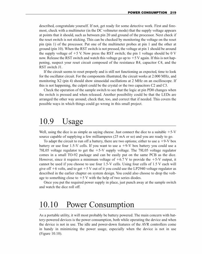
described, congratulate yourself. If not, get ready for some detective work. First and fore-most, check with a multimeter (in the DC voltmeter mode) that the supply voltage appearsat points that it should, such as between pin 20 and ground of the processor. Next check ifthe reset switch is not sticking. This can be checked by monitoring the voltage on the resetpin (pin 1) of the processor. Put one of the multimeter probes at pin 1 and the other atground (pin 10). When the RST switch is not pressed, the voltage at pin 1 should be aroundthe supply voltage of �5 V. Now press the RST switch; the pin 1 voltage should be 0 Vnow. Release the RST switch and watch this voltage go up to �5 V again. If this is not hap-pening, suspect your reset circuit composed of the resistance R4, capacitor C4, and theRST switch J1.
If the circuit seems to reset properly and is still not functioning as expected, time to lookfor the oscillator circuit. For the components illustrated, the circuit works at 2.000 MHz, andmonitoring X2 (pin 4) should show sinusoidal oscillations at 2 MHz on an oscilloscope. Ifthis is not happening, the culprit could be the crystal or the two capacitors C2 and C3.
Check the operation of the sample switch to see that the logic at pin PD0 changes whenthe switch is pressed and when released. Another possibility could be that the LEDs arearranged the other way around; check that, too, and correct that if needed. This covers thepossible ways in which things could go wrong in this small project.
10.9 UsageWell, using the dice is as simple as saying cheese. Just connect the dice to a suitable �5-Vsource capable of supplying a few milliamperes (25 mA or so) and you are ready to go.
To adapt the circuit to run off a battery, there are two options; either to use a �9-V boxbattery or use four 1.5-V cells. If you want to use a �9-V box battery you could use a78L05 voltage regulator to get the �5-V supply voltage. The 78L05 voltage regulatorcomes in a small TO-92 package and can be easily put on the same PCB as the dice.However, since it requires a minimum voltage of �6.7 V to provide the �5-V output, itcannot be used if you choose to use four 1.5-V cells. Using four cells of 1.5 V each willgive off �6 volts, and to get �5 V out of it you could use the LP2940 voltage regulator asdescribed in the earlier chapter on system design. You could also choose to drop the volt-age to something close to �5 V with the help of two series diodes.
Once you put the required power supply in place, just punch away at the sample switchand watch the dice roll off.
10.10 Power ConsumptionAs a portable utility, it will most probably be battery powered. The main concern with bat-tery-powered devices is the power consumption, both while operating the device and whenthe device is not in use. The idle and power-down features of the AVR controllers come in handy in minimizing the power usage, especially when the device is not in use (Figure 10.10).
POWER CONSUMPTION 219
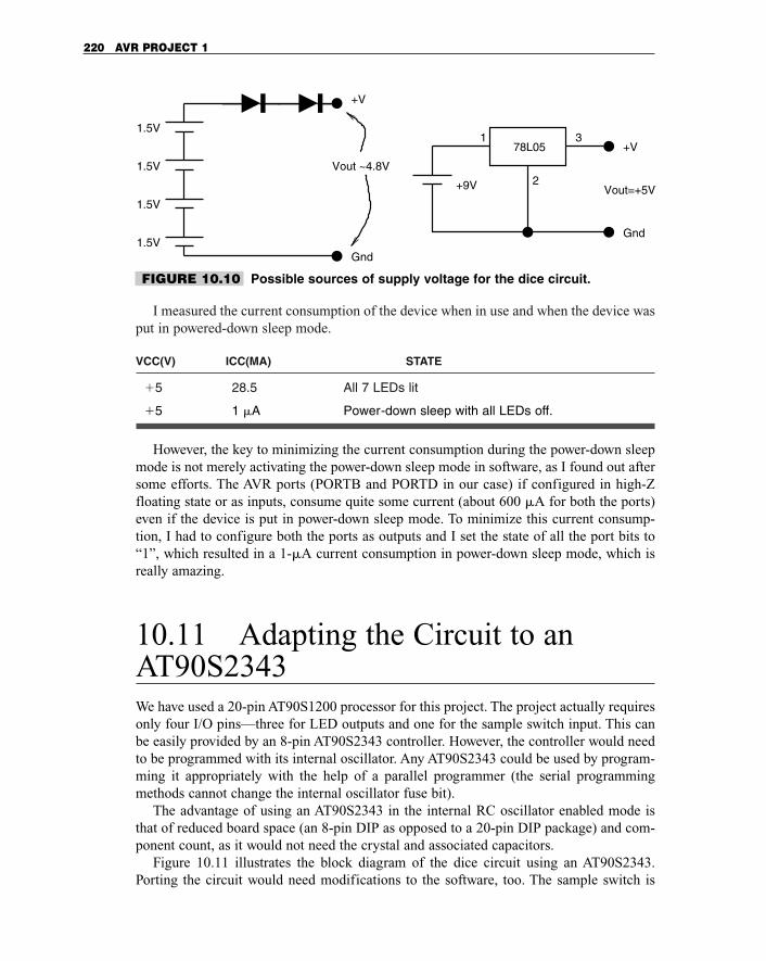
I measured the current consumption of the device when in use and when the device wasput in powered-down sleep mode.
VCC(V) ICC(MA) STATE
�5 28.5 All 7 LEDs lit
�5 1 �A Power-down sleep with all LEDs off.
However, the key to minimizing the current consumption during the power-down sleepmode is not merely activating the power-down sleep mode in software, as I found out aftersome efforts. The AVR ports (PORTB and PORTD in our case) if configured in high-Zfloating state or as inputs, consume quite some current (about 600 �A for both the ports)even if the device is put in power-down sleep mode. To minimize this current consump-tion, I had to configure both the ports as outputs and I set the state of all the port bits to“1”, which resulted in a 1-�A current consumption in power-down sleep mode, which isreally amazing.
10.11 Adapting the Circuit to anAT90S2343We have used a 20-pin AT90S1200 processor for this project. The project actually requiresonly four I/O pins—three for LED outputs and one for the sample switch input. This canbe easily provided by an 8-pin AT90S2343 controller. However, the controller would needto be programmed with its internal oscillator. Any AT90S2343 could be used by program-ming it appropriately with the help of a parallel programmer (the serial programmingmethods cannot change the internal oscillator fuse bit).
The advantage of using an AT90S2343 in the internal RC oscillator enabled mode isthat of reduced board space (an 8-pin DIP as opposed to a 20-pin DIP package) and com-ponent count, as it would not need the crystal and associated capacitors.
Figure 10.11 illustrates the block diagram of the dice circuit using an AT90S2343.Porting the circuit would need modifications to the software, too. The sample switch is
220 AVR PROJECT 1
1.5V
1.5V
1.5V
1.5V
Vout ~4.8V
+V
Gnd
78L051
2
3
+9V Vout=+5V
+V
Gnd
FIGURE 10.10 Possible sources of supply voltage for the dice circuit.
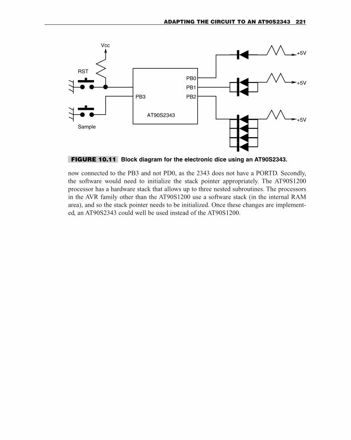
now connected to the PB3 and not PD0, as the 2343 does not have a PORTD. Secondly,the software would need to initialize the stack pointer appropriately. The AT90S1200processor has a hardware stack that allows up to three nested subroutines. The processorsin the AVR family other than the AT90S1200 use a software stack (in the internal RAMarea), and so the stack pointer needs to be initialized. Once these changes are implement-ed, an AT90S2343 could well be used instead of the AT90S1200.
ADAPTING THE CIRCUIT TO AN AT90S2343 221
Vcc
RST
Sample
+5V
+5V
+5V
PB0
PB1
PB2PB3
AT90S2343
FIGURE 10.11 Block diagram for the electronic dice using an AT90S2343.

This page intentionally left blank.
11.1 At a GlanceSalient features of this chapter are:
1. An interesting project for amateur radio enthusiasts.2. Uses an AT90S1200 and sundry components.3. Discusses alternative designs.4. Shows how to modify the circuit and code for an 8-pin AT90S2343 or ATtiny22.
11.2 IntroductionA large number of amateur radio enthusiasts all over the world employ Morse code forradio communications. Morse code is an international system of signals employed in radiotelegraphy in the land-telegraph systems of all countries.
For that they must first learn Morse code. Morse code is a signaling standard usingaudio tones. It relies on tone duration for encoding whatever symbols you want to encode.The code specifies two types of tone durations: a short duration and a long duration. Thelong duration is three times the duration of the short duration tone. The duration of the toneitself is variable, and the actual value determines the speed of transmission. Symbols that
11AVR PROJECT 2: A MORSE KEYER
223
Copyright 2001 The McGraw-Hill Companies, Inc. Click Here for Terms of Use.

are encoded comprise a sequence of short and long tones. The various tones in a symbolare spaced with periods of silence (i.e., periods of no tone). These periods are of the sameduration as the short-duration tone. Symbols separated by no tone period are equal to thatof a long-duration tone. These symbols are called dots and dashes. If a dot is for a time T,then the dash is for a time 3T.
A standard form of Morse code that is acceptable everywhere is called InternationalMorse code. To learn Morse code, you need to listen to the tones for each symbol andremember them.
INTERNATIONAL MORSE CODE FOR THE ALPHABETS
A .- Alfa
B -... Bravo
C -.-. Charlie
D -.. Delta
E . Echo
F ..-. Foxtrot
G --. Golf
H .... Hotel
I .. India
J .--- Juliet
K -.- Kilo
L .-.. Lima
M -- Mike
N -. November
O --- Oscar
P .--. Papa
Q --.- Quebec
R .-. Romeo
S ... Sierra
T - Tango
U ..- Uniform
V ...- Victor
W .-- Whiskey
X -..- X-ray
Y -.-- Yankee
Z --.. Zulu
224 AVR PROJECT 2: A MORSE KEYER
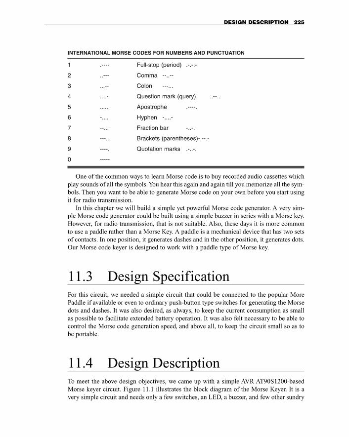
INTERNATIONAL MORSE CODES FOR NUMBERS AND PUNCTUATION
1 .---- Full-stop (period) .-.-.-
2 ..--- Comma --..--
3 ...-- Colon ---...
4 ....- Question mark (query) ..--..
5 ..... Apostrophe .----.
6 -.... Hyphen -....-
7 --... Fraction bar -..-.
8 ---.. Brackets (parentheses)-.--.-
9 ----. Quotation marks .-..-.
0 -----
One of the common ways to learn Morse code is to buy recorded audio cassettes whichplay sounds of all the symbols. You hear this again and again till you memorize all the sym-bols. Then you want to be able to generate Morse code on your own before you start usingit for radio transmission.
In this chapter we will build a simple yet powerful Morse code generator. A very sim-ple Morse code generator could be built using a simple buzzer in series with a Morse key.However, for radio transmission, that is not suitable. Also, these days it is more commonto use a paddle rather than a Morse Key. A paddle is a mechanical device that has two setsof contacts. In one position, it generates dashes and in the other position, it generates dots.Our Morse code keyer is designed to work with a paddle type of Morse key.
11.3 Design SpecificationFor this circuit, we needed a simple circuit that could be connected to the popular MorePaddle if available or even to ordinary push-button type switches for generating the Morsedots and dashes. It was also desired, as always, to keep the current consumption as smallas possible to facilitate extended battery operation. It was also felt necessary to be able tocontrol the Morse code generation speed, and above all, to keep the circuit small so as tobe portable.
11.4 Design DescriptionTo meet the above design objectives, we came up with a simple AVR AT90S1200-basedMorse keyer circuit. Figure 11.1 illustrates the block diagram of the Morse Keyer. It is avery simple circuit and needs only a few switches, an LED, a buzzer, and few other sundry
DESIGN DESCRIPTION 225
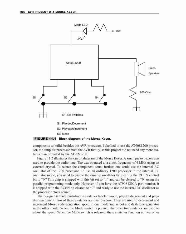
components to build, besides the AVR processor. I decided to use the AT90S1200 proces-sor, the simplest processor from the AVR family, as this project did not need any more fea-tures than provided by the AT90S1200.
Figure 11.2 illustrates the circuit diagram of the Morse Keyer. A small piezo buzzer wasused to provide the audio tone. The was operated at a clock frequency of 4 MHz using anexternal crystal. To reduce the component count further, one could use the internal RCoscillator of the 1200 processor. To use an ordinary 1200 processor in the internal RCoscillator mode, you need to enable the on-chip oscillator by clearing the RCEN controlbit to “0.” This chip is shipped with this bit set to “1” and can be cleared to “0” using theparallel programming mode only. However, if you have the AT90S1200A part number, itis shipped with the RCEN bit cleared to “0” and ready to use the internal RC oscillator asthe processor clock source.
The design has three push-button switches labeled mode, playdot/decrement and play-dash/increment. Two of these switches are dual purpose. They are used to decrement andincrement Morse code generation speed in one mode and as dot and dash tone generatorin the other mode. When the Mode switch is pressed, the other two switches are used toadjust the speed. When the Mode switch is released, these switches function in their other
226 AVR PROJECT 2: A MORSE KEYER
Piezo
Speaker
200 Ohm
+5V
S4S1 S2
S1-S3: Switches
S1: Playdot/Decrement
S2: Playdash/Increment
S3: Mode
AT90S1200
Mode LED
FIGURE 11.1 Block diagram of the Morse Keyer.
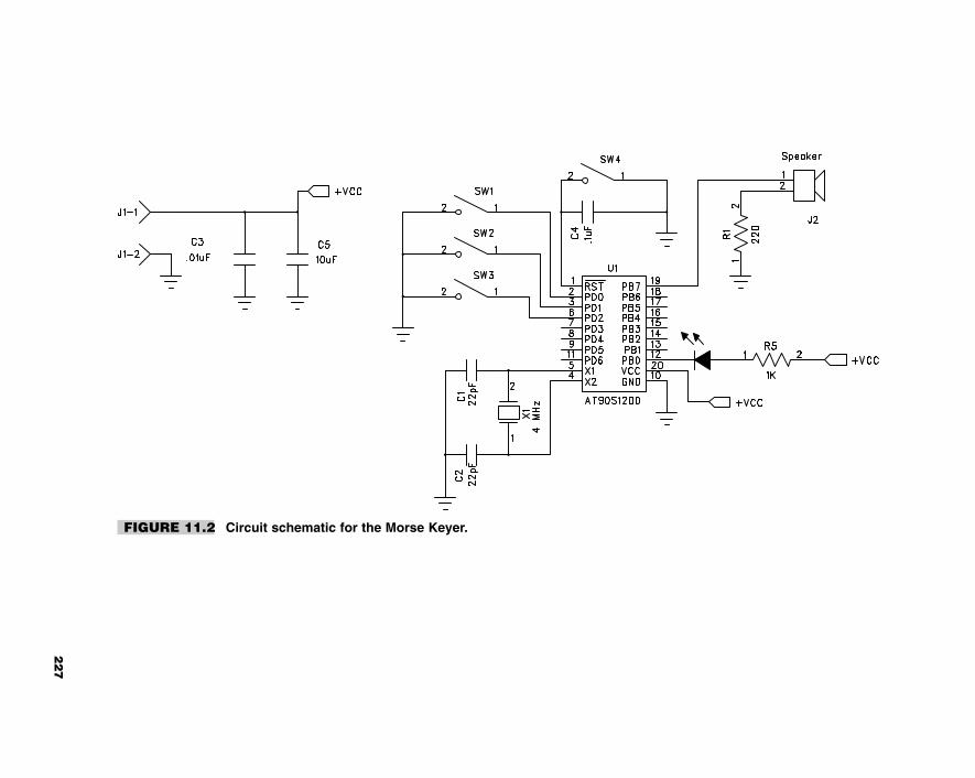
FIGURE 11.2 Circuit schematic for the Morse Keyer.
22
7
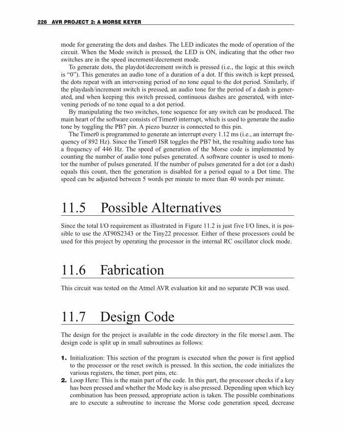
mode for generating the dots and dashes. The LED indicates the mode of operation of thecircuit. When the Mode switch is pressed, the LED is ON, indicating that the other twoswitches are in the speed increment/decrement mode.
To generate dots, the playdot/decrement switch is pressed (i.e., the logic at this switchis “0”). This generates an audio tone of a duration of a dot. If this switch is kept pressed,the dots repeat with an intervening period of no tone equal to the dot period. Similarly, ifthe playdash/increment switch is pressed, an audio tone for the period of a dash is gener-ated, and when keeping this switch pressed, continuous dashes are generated, with inter-vening periods of no tone equal to a dot period.
By manipulating the two switches, tone sequence for any switch can be produced. Themain heart of the software consists of Timer0 interrupt, which is used to generate the audiotone by toggling the PB7 pin. A piezo buzzer is connected to this pin.
The Timer0 is programmed to generate an interrupt every 1.12 ms (i.e., an interrupt fre-quency of 892 Hz). Since the Timer0 ISR toggles the PB7 bit, the resulting audio tone hasa frequency of 446 Hz. The speed of generation of the Morse code is implemented bycounting the number of audio tone pulses generated. A software counter is used to moni-tor the number of pulses generated. If the number of pulses generated for a dot (or a dash)equals this count, then the generation is disabled for a period equal to a Dot time. Thespeed can be adjusted between 5 words per minute to more than 40 words per minute.
11.5 Possible AlternativesSince the total I/O requirement as illustrated in Figure 11.2 is just five I/O lines, it is pos-sible to use the AT90S2343 or the Tiny22 processor. Either of these processors could beused for this project by operating the processor in the internal RC oscillator clock mode.
11.6 FabricationThis circuit was tested on the Atmel AVR evaluation kit and no separate PCB was used.
11.7 Design CodeThe design for the project is available in the code directory in the file morse1.asm. Thedesign code is split up in small subroutines as follows:
1. Initialization: This section of the program is executed when the power is first appliedto the processor or the reset switch is pressed. In this section, the code initializes thevarious registers, the timer, port pins, etc.
2. Loop Here: This is the main part of the code. In this part, the processor checks if a keyhas been pressed and whether the Mode key is also pressed. Depending upon which keycombination has been pressed, appropriate action is taken. The possible combinationsare to execute a subroutine to increase the Morse code generation speed, decrease
228 AVR PROJECT 2: A MORSE KEYER
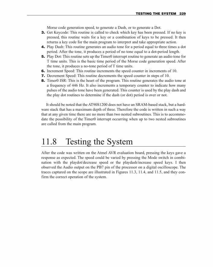
Morse code generation speed, to generate a Dash, or to generate a Dot.3. Get Keycode: This routine is called to check which key has been pressed. If no key is
pressed, this routine waits for a key or a combination of keys to be pressed. It thenreturns a key code for the main program to interpret and take appropriate action.
4. Play Dash: This routine generates an audio tone for a period equal to three times a dotperiod. After the tone, it produces a period of no tone equal to a dot-period length.
5. Play Dot: This routine sets up the Timer0 interrupt routine to generate an audio tone forT time units. This is the basic time period of the Morse code generation speed. Afterthe tone, it produces a no-tone period of T time units.
6. Increment Speed: This routine increments the speed counter in increments of 10.7. Decrement Speed: This routine decrements the speed counter in steps of 10.8. Timer0 ISR: This is the heart of the program. This routine generates the audio tone at
a frequency of 446 Hz. It also increments a temporary counter to indicate how manypulses of the audio tone have been generated. This counter is used by the play dash andthe play dot routines to determine if the dash (or dot) period is over or not.
It should be noted that the AT90S1200 does not have an SRAM-based stack, but a hard-ware stack that has a maximum depth of three. Therefore the code is written in such a waythat at any given time there are no more than two nested subroutines. This is to accommo-date the possibility of the Timer0 interrupt occurring when up to two nested subroutinesare called from the main program.
11.8 Testing the SystemAfter the code was written on the Atmel AVR evaluation board, pressing the keys gave aresponse as expected. The speed could be varied by pressing the Mode switch in combi-nation with the playdot/decrease speed or the playdash/increase speed keys. I thenobserved the Audio output on the PB7 pin of the processor on a digital oscilloscope. Thetraces captured on the scope are illustrated in Figures 11.3, 11.4, and 11.5, and they con-firm the correct operation of the system.
TESTING THE SYSTEM 229
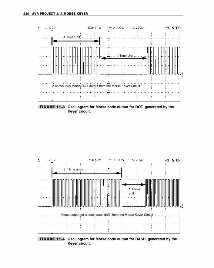
230 AVR PROJECT 2: A MORSE KEYER
1 Time Unit
1 Time Unit
A continuous Morse DOT output from the Morse Keyer Circuit
Morse output for a continuous dash from the Morse Keyer Circuit
3 T time units
1 T timeunit
FIGURE 11.3 Oscillogram for Morse code output for DOT, generated by theKeyer circuit.
FIGURE 11.4 Oscillogram for Morse code output for DASH, generated by theKeyer circuit.
TESTING THE SYSTEM 231
TT T T 3T
Morse output for the letter ‘U’ (di-di-dah) generated by the Morse Keyer
Circuit
FIGURE 11.5 Oscillogram for Morse code output for the character U, generatedby the Keyer circuit.

This page intentionally left blank.
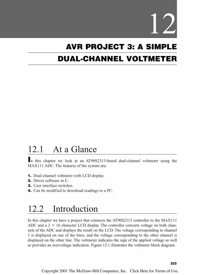
12.1 At a GlanceIn this chapter we look at an AT90S2313-based dual-channel voltmeter using theMAX111 ADC. The features of the system are:
1. Dual-channel voltmeter with LCD display.2. Driver software in C.3. User interface switches.4. Can be modified to download readings to a PC.
12.2 IntroductionIn this chapter we have a project that connects the AT90S2313 controller to the MAX111ADC and a 2 � 16 character LCD display. The controller converts voltage on both chan-nels of the ADC and displays the result on the LCD. The voltage corresponding to channel1 is displayed on one of the lines, and the voltage corresponding to the other channel isdisplayed on the other line. The voltmeter indicates the sign of the applied voltage as wellas provides an overvoltage indication. Figure 12.1 illustrates the voltmeter block diagram.
12AVR PROJECT 3: A SIMPLE
DUAL-CHANNEL VOLTMETER
233
Copyright 2001 The McGraw-Hill Companies, Inc. Click Here for Terms of Use.
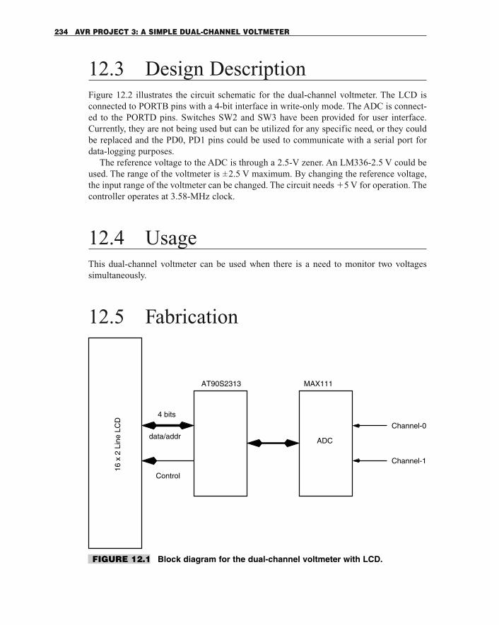
12.3 Design DescriptionFigure 12.2 illustrates the circuit schematic for the dual-channel voltmeter. The LCD isconnected to PORTB pins with a 4-bit interface in write-only mode. The ADC is connect-ed to the PORTD pins. Switches SW2 and SW3 have been provided for user interface.Currently, they are not being used but can be utilized for any specific need, or they couldbe replaced and the PD0, PD1 pins could be used to communicate with a serial port fordata-logging purposes.
The reference voltage to the ADC is through a 2.5-V zener. An LM336-2.5 V could beused. The range of the voltmeter is ±2.5 V maximum. By changing the reference voltage,the input range of the voltmeter can be changed. The circuit needs �5 V for operation. Thecontroller operates at 3.58-MHz clock.
12.4 UsageThis dual-channel voltmeter can be used when there is a need to monitor two voltagessimultaneously.
12.5 Fabrication
234 AVR PROJECT 3: A SIMPLE DUAL-CHANNEL VOLTMETER
16 x
2 L
ine
LCD
4 bits
Control
AT90S2313 MAX111
ADC
Channel-1
Channel-0data/addr
FIGURE 12.1 Block diagram for the dual-channel voltmeter with LCD.
The voltmeter was fabricated on a general-purpose PCB about 2 inches a side, and thecompleted circuit board is illustrated in Figure 12.3.
12.6 Design CodeThe code for this project was written in C using the SPJ systems’ C-AVR compiler and isavailable in the code directory in the file adc.c. Figure 12.4 illustrates the MAX111 ADCsignals as captured on a logic analyzer.
DESIGN CODE 235
FIGURE 12.2 Circuit schematic for a the dual-channel voltmeter with an LCD display.
23
6
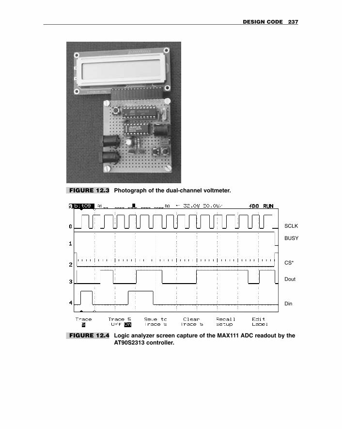
DESIGN CODE 237
SCLK
BUSY
CS*
Dout
Din
FIGURE 12.3 Photograph of the dual-channel voltmeter.
FIGURE 12.4 Logic analyzer screen capture of the MAX111 ADC readout by theAT90S2313 controller.

This page intentionally left blank.
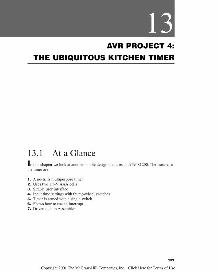
13.1 At a GlanceIn this chapter we look at another simple design that uses an AT90S1200. The features ofthe timer are:
1. A no-frills multipurpose timer2. Uses two 1.5-V AAA cells3. Simple user interface4. Input time settings with thumb-wheel switches5. Timer is armed with a single switch6. Shows how to use an interrupt7. Driver code in Assembler
13AVR PROJECT 4:
THE UBIQUITOUS KITCHEN TIMER
239
Copyright 2001 The McGraw-Hill Companies, Inc. Click Here for Terms of Use.
13.2 IntroductionTime is money. In the kitchen, knowing time could mean you have an unburnt, properlycooked dish (whether it tastes good is another matter).
Toward that end, we have a small and useful project that will allow you to keep goodtime. Besides in the kitchen, you could use it elsewhere, as a siesta alarm for example.
This design of an interval timer is kept very simple with no frills. Perhaps it doesn’t getsimpler than this design. Figure 13.1 illustrates the block diagram of the design.
Thumb-wheel switches are used to enter the time in minutes (nothing cooks in secondsanyway!). Once you set the required time, just reset the timer and it starts counting. Oncethe set time has elapsed, the buzzer goes on.
13.3 Design DescriptionThe design of the timer is very simple. Figure 13.2 illustrates the circuit schematic. Onlya handful of components are required to build the Timer. To keep the system simple, wehave used thumb-wheel switches to input the time. More fancy solutions involving a key-pad and an LCD display are also possible, but that leads to a bigger circuit and one whichconsumes more current.
The thumb-wheel switches are connected to the PORTB pins. Each thumb-wheel switchrequires four pins to read. So the entire PORTB is used up. The PORTB is programmed as aninput port with the pull-up resistors on. This means that external resistors are not required.
240 AVR PROJECT 4: THE UBIQUITOUS KITCHEN TIMER
Thumb-
Wheel
Switch
Thumb-
Wheel
Switch
3.58 MHz
RESET
AT90S1200
Piezo
Buzzer
FIGURE 13.1 Block diagram of the simple kitchen timer.
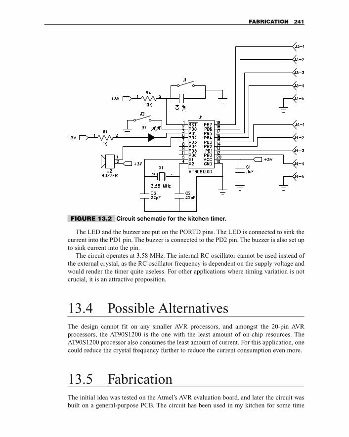
The LED and the buzzer are put on the PORTD pins. The LED is connected to sink thecurrent into the PD1 pin. The buzzer is connected to the PD2 pin. The buzzer is also set upto sink current into the pin.
The circuit operates at 3.58 MHz. The internal RC oscillator cannot be used instead ofthe external crystal, as the RC oscillator frequency is dependent on the supply voltage andwould render the timer quite useless. For other applications where timing variation is notcrucial, it is an attractive proposition.
13.4 Possible AlternativesThe design cannot fit on any smaller AVR processors, and amongst the 20-pin AVRprocessors, the AT90S1200 is the one with the least amount of on-chip resources. TheAT90S1200 processor also consumes the least amount of current. For this application, onecould reduce the crystal frequency further to reduce the current consumption even more.
13.5 FabricationThe initial idea was tested on the Atmel’s AVR evaluation board, and later the circuit wasbuilt on a general-purpose PCB. The circuit has been used in my kitchen for some time
FABRICATION 241
FIGURE 13.2 Circuit schematic for the kitchen timer.
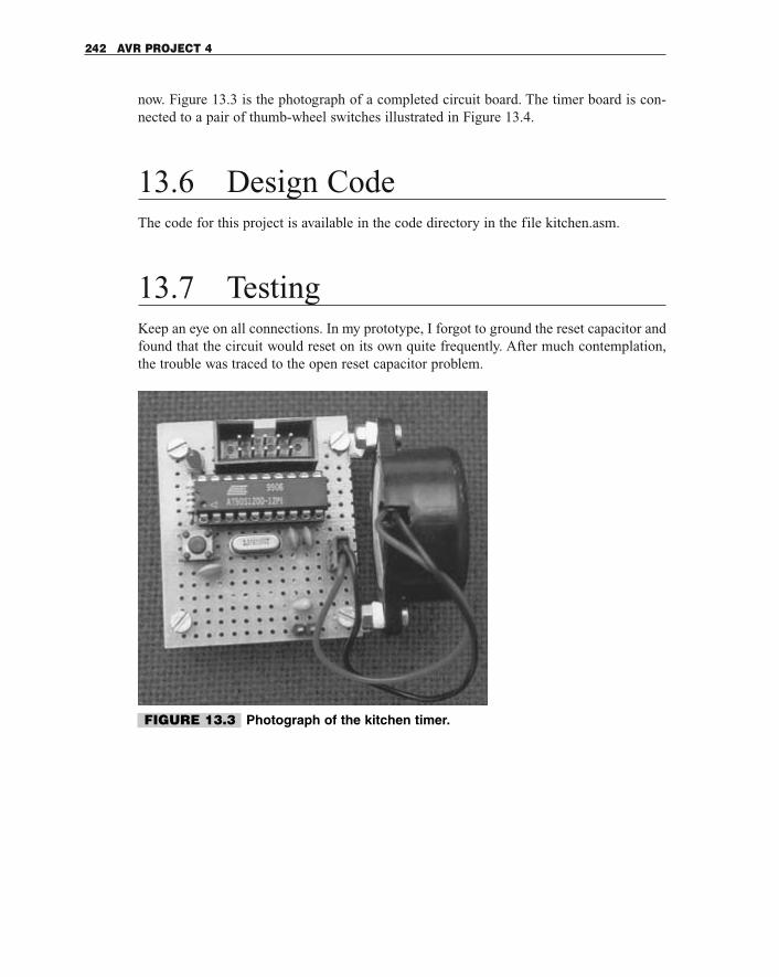
now. Figure 13.3 is the photograph of a completed circuit board. The timer board is con-nected to a pair of thumb-wheel switches illustrated in Figure 13.4.
13.6 Design CodeThe code for this project is available in the code directory in the file kitchen.asm.
13.7 TestingKeep an eye on all connections. In my prototype, I forgot to ground the reset capacitor andfound that the circuit would reset on its own quite frequently. After much contemplation,the trouble was traced to the open reset capacitor problem.
242 AVR PROJECT 4
FIGURE 13.3 Photograph of the kitchen timer.
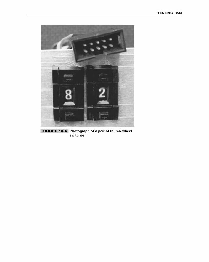
TESTING 243
FIGURE 13.4 Photograph of a pair of thumb-wheelswitches

This page intentionally left blank.
14.1 At a GlanceIn this chapter we consider the following issues:
1. What is a radio beacon?2. What is a radio beacon used for?3. How to build a radio beacon controller.4. Details of an efficient and compact single-chip radio beacon controller.5. How to adapt the controller for your application.
14.2 IntroductionMerriam Webster’s Collegiate Dictionary defines a beacon as a signal fire or other signalcommonly on a hill, tower, or pole for guidance. A radio beacon is a radio transmitter emit-ting signals for guidance of an aircraft. However, a radio beacon is used for more than air-craft guidance.
A radio beacon is usually put on scientific balloons, rockets, etc., for identification aswell as help in locating the object (i.e., the balloon or the rocket). Usually the beacon
14AVR PROJECT 5:
RADIO BEACON CONTROLLER
245
Copyright 2001 The McGraw-Hill Companies, Inc. Click Here for Terms of Use.
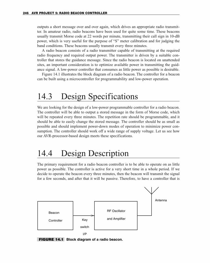
outputs a short message over and over again, which drives an appropriate radio transmit-ter. In amateur radio, radio beacons have been used for quite some time. These beaconsusually transmit Morse code at 22 words per minute, transmitting their call sign in 10-dBpower, which is very useful for the purpose of “S” meter calibration and for judging theband conditions. These beacons usually transmit every three minutes.
A radio beacon consists of a radio transmitter capable of transmitting at the requiredradio frequency and required output power. The transmitter is driven by a suitable con-troller that stores the guidance message. Since the radio beacon is located on unattendedsites, an important consideration is to optimize available power in transmitting the guid-ance signal. A low-power controller that consumes as little power as possible is desirable.
Figure 14.1 illustrates the block diagram of a radio beacon. The controller for a beaconcan be built using a microcontroller for programmability and low-power operation.
14.3 Design SpecificationsWe are looking for the design of a low-power programmable controller for a radio beacon.The controller will be able to output a stored message in the form of Morse code, whichwill be repeated every three minutes. The repetition rate should be programmable, and itshould be able to easily change the stored message. The controller should be as small aspossible and should implement power-down modes of operation to minimize power con-sumption. The controller should work off a wide range of supply voltage. Let us see howour AVR-processor-based design meets these specifications.
14.4 Design DescriptionThe primary requirement for a radio beacon controller is to be able to operate on as littlepower as possible. The controller is active for a very short time in a whole period. If wedecide to operate the beacon every three minutes, then the beacon will transmit the signalfor a few seconds, and after that it will be passive. Therefore, to have a controller that is
246 AVR PROJECT 5: RADIO BEACON CONTROLLER
Beacon
Controller
RF Oscillator
and AmplifierKey
I/P
switch
Antenna
FIGURE 14.1 Block diagram of a radio beacon.
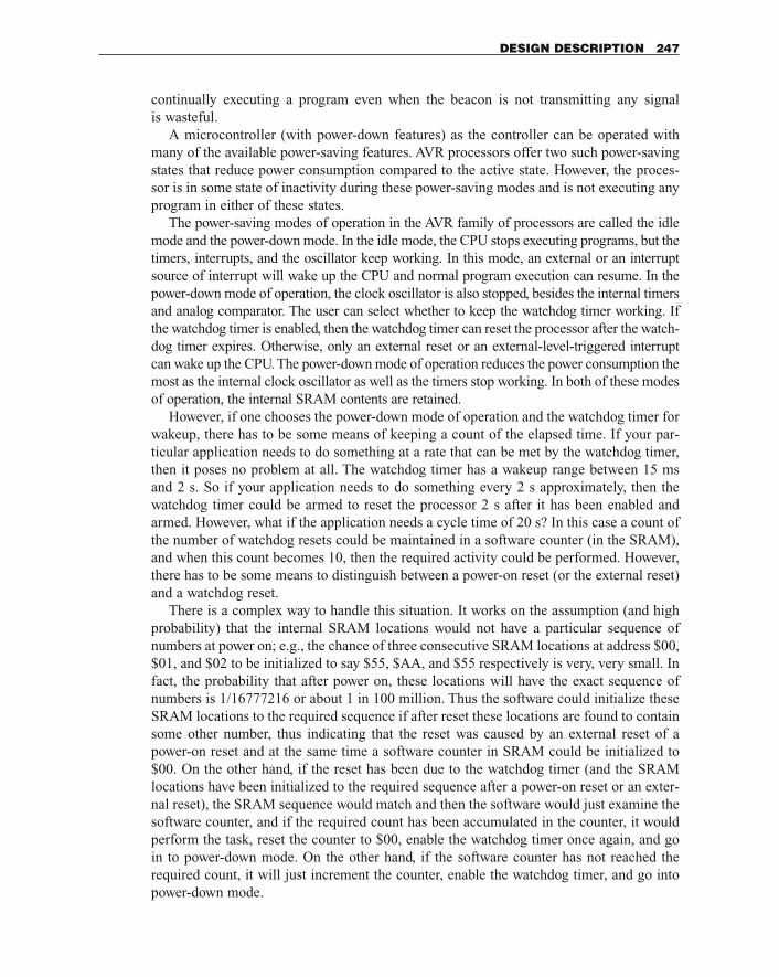
continually executing a program even when the beacon is not transmitting any signal is wasteful.
A microcontroller (with power-down features) as the controller can be operated withmany of the available power-saving features. AVR processors offer two such power-savingstates that reduce power consumption compared to the active state. However, the proces-sor is in some state of inactivity during these power-saving modes and is not executing anyprogram in either of these states.
The power-saving modes of operation in the AVR family of processors are called the idlemode and the power-down mode. In the idle mode, the CPU stops executing programs, but thetimers, interrupts, and the oscillator keep working. In this mode, an external or an interruptsource of interrupt will wake up the CPU and normal program execution can resume. In thepower-down mode of operation, the clock oscillator is also stopped, besides the internal timersand analog comparator. The user can select whether to keep the watchdog timer working. Ifthe watchdog timer is enabled, then the watchdog timer can reset the processor after the watch-dog timer expires. Otherwise, only an external reset or an external-level-triggered interruptcan wake up the CPU. The power-down mode of operation reduces the power consumption themost as the internal clock oscillator as well as the timers stop working. In both of these modesof operation, the internal SRAM contents are retained.
However, if one chooses the power-down mode of operation and the watchdog timer forwakeup, there has to be some means of keeping a count of the elapsed time. If your par-ticular application needs to do something at a rate that can be met by the watchdog timer,then it poses no problem at all. The watchdog timer has a wakeup range between 15 msand 2 s. So if your application needs to do something every 2 s approximately, then thewatchdog timer could be armed to reset the processor 2 s after it has been enabled andarmed. However, what if the application needs a cycle time of 20 s? In this case a count ofthe number of watchdog resets could be maintained in a software counter (in the SRAM),and when this count becomes 10, then the required activity could be performed. However,there has to be some means to distinguish between a power-on reset (or the external reset)and a watchdog reset.
There is a complex way to handle this situation. It works on the assumption (and highprobability) that the internal SRAM locations would not have a particular sequence ofnumbers at power on; e.g., the chance of three consecutive SRAM locations at address $00,$01, and $02 to be initialized to say $55, $AA, and $55 respectively is very, very small. Infact, the probability that after power on, these locations will have the exact sequence ofnumbers is 1/16777216 or about 1 in 100 million. Thus the software could initialize theseSRAM locations to the required sequence if after reset these locations are found to containsome other number, thus indicating that the reset was caused by an external reset of apower-on reset and at the same time a software counter in SRAM could be initialized to$00. On the other hand, if the reset has been due to the watchdog timer (and the SRAMlocations have been initialized to the required sequence after a power-on reset or an exter-nal reset), the SRAM sequence would match and then the software would just examine thesoftware counter, and if the required count has been accumulated in the counter, it wouldperform the task, reset the counter to $00, enable the watchdog timer once again, and goin to power-down mode. On the other hand, if the software counter has not reached therequired count, it will just increment the counter, enable the watchdog timer, and go intopower-down mode.
DESIGN DESCRIPTION 247
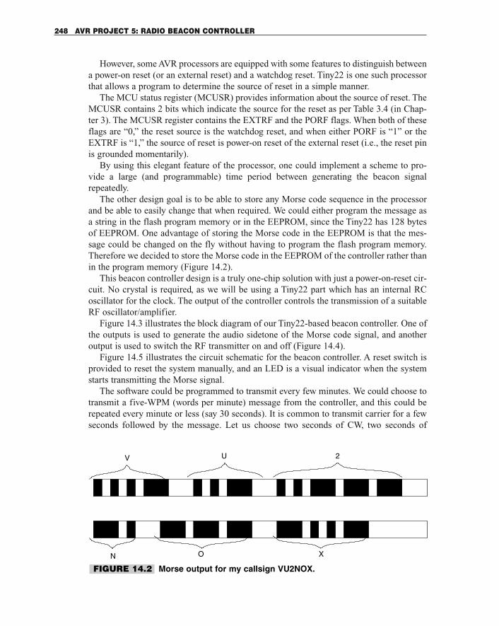
However, some AVR processors are equipped with some features to distinguish betweena power-on reset (or an external reset) and a watchdog reset. Tiny22 is one such processorthat allows a program to determine the source of reset in a simple manner.
The MCU status register (MCUSR) provides information about the source of reset. TheMCUSR contains 2 bits which indicate the source for the reset as per Table 3.4 (in Chap-ter 3). The MCUSR register contains the EXTRF and the PORF flags. When both of theseflags are “0,” the reset source is the watchdog reset, and when either PORF is “1” or theEXTRF is “1,” the source of reset is power-on reset of the external reset (i.e., the reset pinis grounded momentarily).
By using this elegant feature of the processor, one could implement a scheme to pro-vide a large (and programmable) time period between generating the beacon signal repeatedly.
The other design goal is to be able to store any Morse code sequence in the processorand be able to easily change that when required. We could either program the message asa string in the flash program memory or in the EEPROM, since the Tiny22 has 128 bytesof EEPROM. One advantage of storing the Morse code in the EEPROM is that the mes-sage could be changed on the fly without having to program the flash program memory.Therefore we decided to store the Morse code in the EEPROM of the controller rather thanin the program memory (Figure 14.2).
This beacon controller design is a truly one-chip solution with just a power-on-reset cir-cuit. No crystal is required, as we will be using a Tiny22 part which has an internal RCoscillator for the clock. The output of the controller controls the transmission of a suitableRF oscillator/amplifier.
Figure 14.3 illustrates the block diagram of our Tiny22-based beacon controller. One ofthe outputs is used to generate the audio sidetone of the Morse code signal, and anotheroutput is used to switch the RF transmitter on and off (Figure 14.4).
Figure 14.5 illustrates the circuit schematic for the beacon controller. A reset switch isprovided to reset the system manually, and an LED is a visual indicator when the systemstarts transmitting the Morse signal.
The software could be programmed to transmit every few minutes. We could choose totransmit a five-WPM (words per minute) message from the controller, and this could berepeated every minute or less (say 30 seconds). It is common to transmit carrier for a fewseconds followed by the message. Let us choose two seconds of CW, two seconds of
248 AVR PROJECT 5: RADIO BEACON CONTROLLER
N X
2V U
O
FIGURE 14.2 Morse output for my callsign VU2NOX.
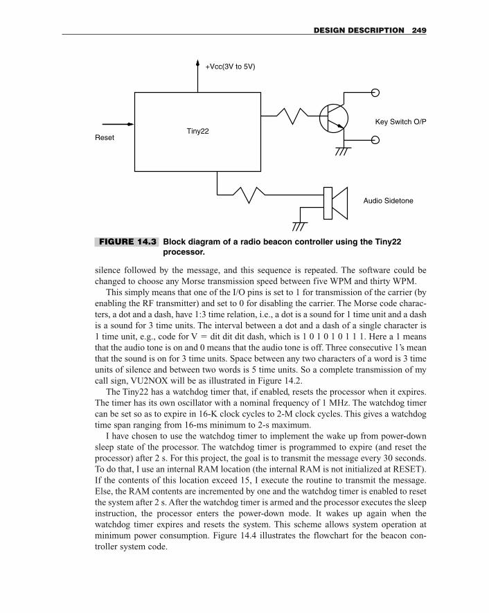
silence followed by the message, and this sequence is repeated. The software could bechanged to choose any Morse transmission speed between five WPM and thirty WPM.
This simply means that one of the I/O pins is set to 1 for transmission of the carrier (byenabling the RF transmitter) and set to 0 for disabling the carrier. The Morse code charac-ters, a dot and a dash, have 1:3 time relation, i.e., a dot is a sound for 1 time unit and a dashis a sound for 3 time units. The interval between a dot and a dash of a single character is1 time unit, e.g., code for V � dit dit dit dash, which is 1 0 1 0 1 0 1 1 1. Here a 1 meansthat the audio tone is on and 0 means that the audio tone is off. Three consecutive 1’s meanthat the sound is on for 3 time units. Space between any two characters of a word is 3 timeunits of silence and between two words is 5 time units. So a complete transmission of mycall sign, VU2NOX will be as illustrated in Figure 14.2.
The Tiny22 has a watchdog timer that, if enabled, resets the processor when it expires.The timer has its own oscillator with a nominal frequency of 1 MHz. The watchdog timercan be set so as to expire in 16-K clock cycles to 2-M clock cycles. This gives a watchdogtime span ranging from 16-ms minimum to 2-s maximum.
I have chosen to use the watchdog timer to implement the wake up from power-downsleep state of the processor. The watchdog timer is programmed to expire (and reset theprocessor) after 2 s. For this project, the goal is to transmit the message every 30 seconds.To do that, I use an internal RAM location (the internal RAM is not initialized at RESET).If the contents of this location exceed 15, I execute the routine to transmit the message.Else, the RAM contents are incremented by one and the watchdog timer is enabled to resetthe system after 2 s. After the watchdog timer is armed and the processor executes the sleepinstruction, the processor enters the power-down mode. It wakes up again when the watchdog timer expires and resets the system. This scheme allows system operation atminimum power consumption. Figure 14.4 illustrates the flowchart for the beacon con-troller system code.
DESIGN DESCRIPTION 249
Tiny22
+Vcc(3V to 5V)
Reset
Key Switch O/P
Audio Sidetone
FIGURE 14.3 Block diagram of a radio beacon controller using the Tiny22processor.
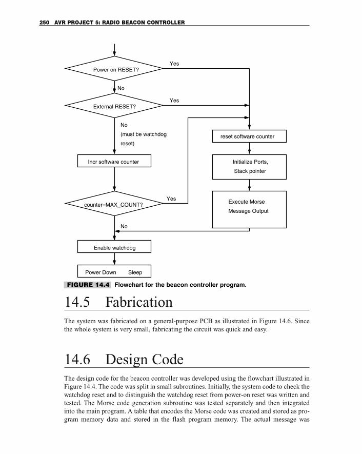
14.5 FabricationThe system was fabricated on a general-purpose PCB as illustrated in Figure 14.6. Sincethe whole system is very small, fabricating the circuit was quick and easy.
14.6 Design CodeThe design code for the beacon controller was developed using the flowchart illustrated inFigure 14.4. The code was split in small subroutines. Initially, the system code to check thewatchdog reset and to distinguish the watchdog reset from power-on reset was written andtested. The Morse code generation subroutine was tested separately and then integratedinto the main program. A table that encodes the Morse code was created and stored as pro-gram memory data and stored in the flash program memory. The actual message was
250 AVR PROJECT 5: RADIO BEACON CONTROLLER
Power on RESET?
External RESET?
No
Yes
Yes
No
Incr software counter
reset software counter
Initialize Ports,
Stack pointer
Yes
No
Enable watchdog
Execute Morse
Message Output
Power Down Sleep
(must be watchdog
reset)
counter=MAX_COUNT?
FIGURE 14.4 Flowchart for the beacon controller program.
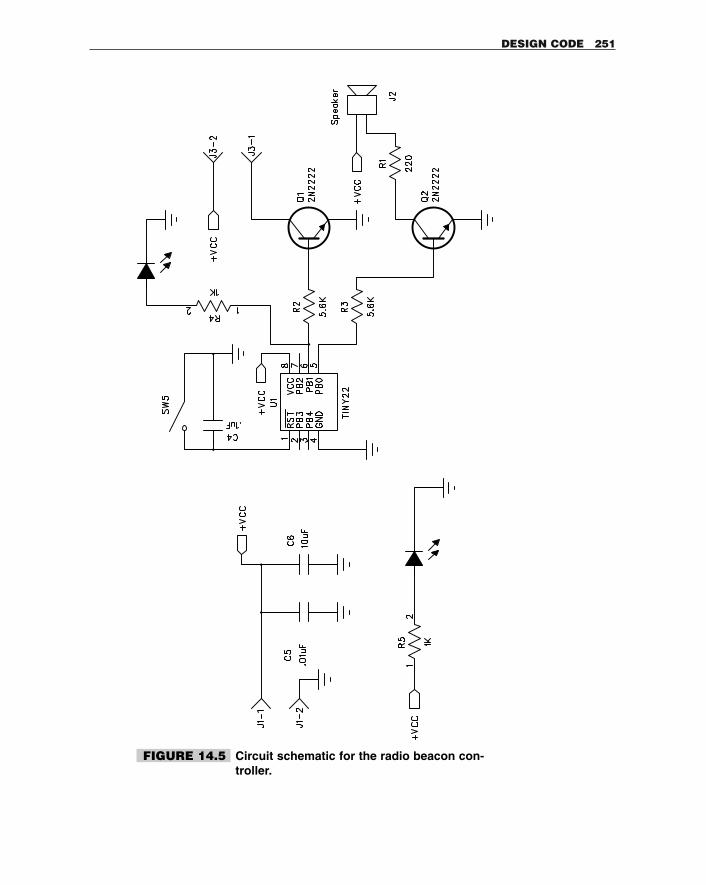
DESIGN CODE 251
FIGURE 14.5 Circuit schematic for the radio beacon con-troller.
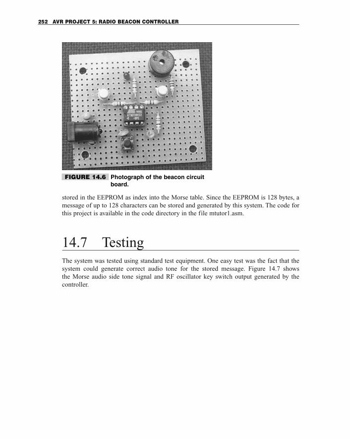
stored in the EEPROM as index into the Morse table. Since the EEPROM is 128 bytes, amessage of up to 128 characters can be stored and generated by this system. The code forthis project is available in the code directory in the file mtutor1.asm.
14.7 TestingThe system was tested using standard test equipment. One easy test was the fact that thesystem could generate correct audio tone for the stored message. Figure 14.7 shows the Morse audio side tone signal and RF oscillator key switch output generated by the controller.
252 AVR PROJECT 5: RADIO BEACON CONTROLLER
FIGURE 14.6 Photograph of the beacon circuitboard.
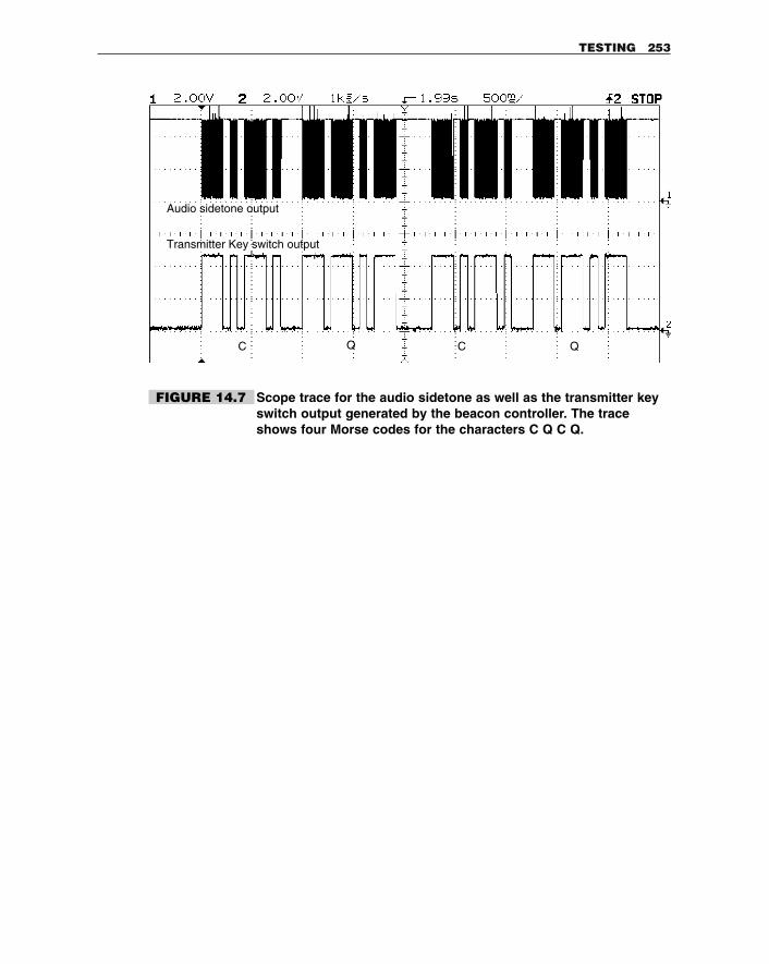
TESTING 253
Transmitter Key switch output
Audio sidetone output
Q C QC
FIGURE 14.7 Scope trace for the audio sidetone as well as the transmitter keyswitch output generated by the beacon controller. The traceshows four Morse codes for the characters C Q C Q.

This page intentionally left blank.
15.1 At a GlanceAll about data acquisition systems
1. Describe a matchbox-size low-power DAS using only 3 ICs2. A complete DAS for astronomical applications3. An OS-independent readout using an RS-232 port
15.2 IntroductionThere are occasions when it is necessary to record data in an unattended manner overextended periods of time.1 Such requirements can often be met with a suitable data acqui-sition system connected to a PC. Often enough, there are occasions to log such data inremote wilderness with no access to suitable power. Such requirement can be met with anautonomous data acquisition system that runs off battery power.
15AVR PROJECT 6: ASTRODAT:
A STAND-ALONE DATA
ACQUISITION SYSTEM
255
1As Ambrose Bierce might have said, “The code presented in this chapter was developed by Saurabh Jain andSmita Mohan and to whom is rightly due the credit for the merit that it may have.”
Copyright 2001 The McGraw-Hill Companies, Inc. Click Here for Terms of Use.
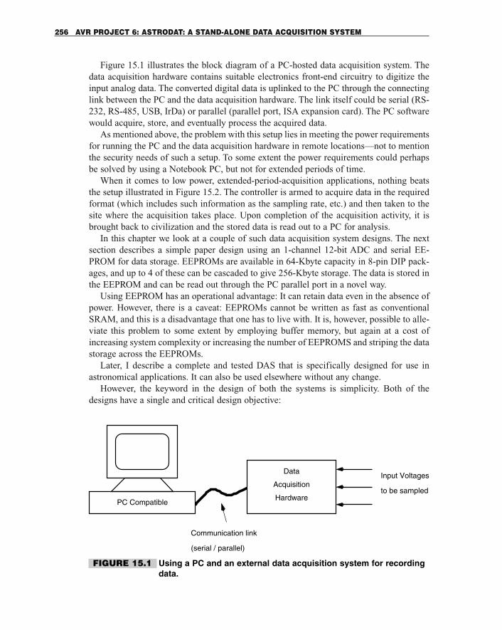
Figure 15.1 illustrates the block diagram of a PC-hosted data acquisition system. Thedata acquisition hardware contains suitable electronics front-end circuitry to digitize theinput analog data. The converted digital data is uplinked to the PC through the connectinglink between the PC and the data acquisition hardware. The link itself could be serial (RS-232, RS-485, USB, IrDa) or parallel (parallel port, ISA expansion card). The PC softwarewould acquire, store, and eventually process the acquired data.
As mentioned above, the problem with this setup lies in meeting the power requirementsfor running the PC and the data acquisition hardware in remote locations—not to mentionthe security needs of such a setup. To some extent the power requirements could perhapsbe solved by using a Notebook PC, but not for extended periods of time.
When it comes to low power, extended-period-acquisition applications, nothing beatsthe setup illustrated in Figure 15.2. The controller is armed to acquire data in the requiredformat (which includes such information as the sampling rate, etc.) and then taken to thesite where the acquisition takes place. Upon completion of the acquisition activity, it isbrought back to civilization and the stored data is read out to a PC for analysis.
In this chapter we look at a couple of such data acquisition system designs. The nextsection describes a simple paper design using an 1-channel 12-bit ADC and serial EE-PROM for data storage. EEPROMs are available in 64-Kbyte capacity in 8-pin DIP pack-ages, and up to 4 of these can be cascaded to give 256-Kbyte storage. The data is stored inthe EEPROM and can be read out through the PC parallel port in a novel way.
Using EEPROM has an operational advantage: It can retain data even in the absence ofpower. However, there is a caveat: EEPROMs cannot be written as fast as conventionalSRAM, and this is a disadvantage that one has to live with. It is, however, possible to alle-viate this problem to some extent by employing buffer memory, but again at a cost ofincreasing system complexity or increasing the number of EEPROMS and striping the datastorage across the EEPROMs.
Later, I describe a complete and tested DAS that is specifically designed for use inastronomical applications. It can also be used elsewhere without any change.
However, the keyword in the design of both the systems is simplicity. Both of thedesigns have a single and critical design objective:
256 AVR PROJECT 6: ASTRODAT: A STAND-ALONE DATA ACQUISITION SYSTEM
Data
AcquisitionInput Voltages
to be sampled
PC Compatible
Communication link
(serial / parallel)
Hardware
FIGURE 15.1 Using a PC and an external data acquisition system for recordingdata.
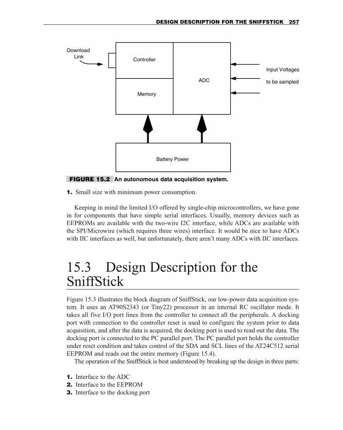
1. Small size with minimum power consumption.
Keeping in mind the limited I/O offered by single-chip microcontrollers, we have gonein for components that have simple serial interfaces. Usually, memory devices such asEEPROMs are available with the two-wire I2C interface, while ADCs are available withthe SPI/Microwire (which requires three wires) interface. It would be nice to have ADCswith IIC interfaces as well, but unfortunately, there aren’t many ADCs with IIC interfaces.
15.3 Design Description for theSniffStickFigure 15.3 illustrates the block diagram of SniffStick, our low-power data acquisition sys-tem. It uses an AT90S2343 (or Tiny22) processor in an internal RC oscillator mode. Ittakes all five I/O port lines from the controller to connect all the peripherals. A dockingport with connection to the controller reset is used to configure the system prior to dataacquisition, and after the data is acquired, the docking port is used to read out the data. Thedocking port is connected to the PC parallel port. The PC parallel port holds the controllerunder reset condition and takes control of the SDA and SCL lines of the AT24C512 serialEEPROM and reads out the entire memory (Figure 15.4).
The operation of the SniffStick is best understood by breaking up the design in three parts:
1. Interface to the ADC2. Interface to the EEPROM3. Interface to the docking port
DESIGN DESCRIPTION FOR THE SNIFFSTICK 257
Input Voltages
to be sampled
Controller
Memory
ADC
LinkDownload
Battery Power
FIGURE 15.2 An autonomous data acquisition system.
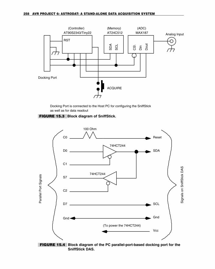
258 AVR PROJECT 6: ASTRODAT: A STAND-ALONE DATA ACQUISITION SYSTEM
RST
MAX187 Analog Input
Docking Port
(Memory) (ADC)
SC
L
SD
A
ACQUIRE
Docking Port is connected to the Host PC for configuring the SniffStickas well as for data readout
(Controller)AT24C512AT90S2343/Tiny22
CS
\
Din
Dou
t
Reset
SDA
SCL
100 Ohm
C0
D0
C1
C2
S7
D7
74HCT244
74HCT244
Gnd Gnd
Vcc
Par
alle
l Por
t Sig
nals
Sig
nals
on
Sni
ffStic
k D
AS
(To power the 74HCT244)
FIGURE 15.3 Block diagram of SniffStick.
FIGURE 15.4 Block diagram of the PC parallel-port-based docking port for theSniffStick DAS.
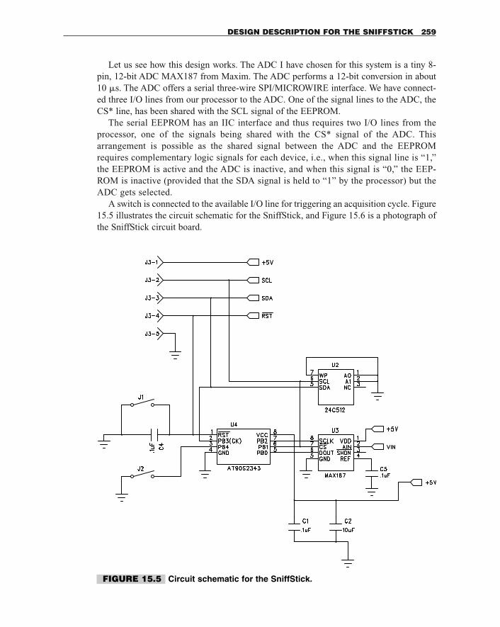
Let us see how this design works. The ADC I have chosen for this system is a tiny 8-pin, 12-bit ADC MAX187 from Maxim. The ADC performs a 12-bit conversion in about10 �s. The ADC offers a serial three-wire SPI/MICROWIRE interface. We have connect-ed three I/O lines from our processor to the ADC. One of the signal lines to the ADC, theCS* line, has been shared with the SCL signal of the EEPROM.
The serial EEPROM has an IIC interface and thus requires two I/O lines from theprocessor, one of the signals being shared with the CS* signal of the ADC. Thisarrangement is possible as the shared signal between the ADC and the EEPROMrequires complementary logic signals for each device, i.e., when this signal line is “1,”the EEPROM is active and the ADC is inactive, and when this signal is “0,” the EEP-ROM is inactive (provided that the SDA signal is held to “1” by the processor) but theADC gets selected.
A switch is connected to the available I/O line for triggering an acquisition cycle. Figure15.5 illustrates the circuit schematic for the SniffStick, and Figure 15.6 is a photograph ofthe SniffStick circuit board.
DESIGN DESCRIPTION FOR THE SNIFFSTICK 259
FIGURE 15.5 Circuit schematic for the SniffStick.
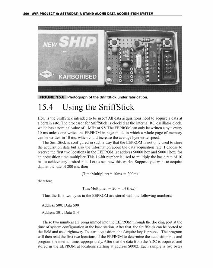
15.4 Using the SniffStickHow is the SniffStick intended to be used? All data acquisitions need to acquire a data ata certain rate. The processor for SniffStick is clocked at the internal RC oscillator clock,which has a nominal value of 1 MHz at 5 V. The EEPROM can only be written a byte every10 ms unless one writes the EEPROM in page mode in which a whole page of memorycan be written in 10 ms, which could increase the average byte write speed.
The SniffStick is configured in such a way that the EEPROM is not only used to storethe acquisition data but also the information about the data acquisition rate. I choose toreserve the first two locations in the EEPROM (at address $0000 hex and $0001 hex) foran acquisition time multiplier. This 16-bit number is used to multiply the basic rate of 10ms to achieve any desired rate. Let us see how this works. Suppose you want to acquiredata at the rate of 200 ms, then
(TimeMultiplier) * 10ms � 200ms
therefore,
TimeMultiplier � 20 � 14 (hex) :
Thus the first two bytes in the EEPROM are stored with the following numbers:
Address $00: Data $00
Address $01: Data $14
These two numbers are programmed into the EEPROM through the docking port at thetime of system configuration at the base station. After that, the SniffStick can be ported tothe field and used rightaway. To start acquisition, the Acquire key is pressed. The programwill then read the first two locations of the EEPROM to determine the acquisition rate andprogram the internal timer appropriately. After that the data from the ADC is acquired andstored in the EEPROM at locations starting at address $0002. Each sample is two bytes
260 AVR PROJECT 6: ASTRODAT: A STAND-ALONE DATA ACQUISITION SYSTEM
FIGURE 15.6 Photograph of the SniffStick under fabrication.
wide (to accommodate the 12-bit ADC result). Between acquisition cycles, the processorgoes in sleep mode to conserve power. After the entire memory has been filled up, theprocessor goes into sleep mode and can be now brought back to the base station and thestored data read out through the Docking port. The next section describes a complete DASon similar principles, but with some modifications to accommodate more features.
15.5 AstroDat: A Complete DAS forAstronomical ApplicationThe SniffStick DAS is an interesting and useful piece of hardware. However, for certainastronomical data acquisition applications, we needed something more than SniffStickcould offer, namely a time-stamping facility as well as the ability to store multiple obser-vation data in a single memory device.
The particular astronomical observation that I am referring to is photometric data log-ging. A photometer is an instrument that converts light to voltage. Astronomical photome-ters are low-noise devices that are capable of detecting faint light intensities emanatingfrom stars and other objects in the sky.
Typically, for an astronomical data acquisition run, you would like to record data relat-ed to many different stars and objects in a single night of observation. Besides, you wouldalso like to record the ambient night sky brightness as a reference.
This means that the date-recording system should have the ability to start and stop aparticular observation and maintain these different sets, which could be separated out later.
To accommodate this feature, I modified the basic SniffStick design to incorporate anRTC and an extra switch. To do this I had to migrate to a bigger processor with more I/Olines. Figure 15.7 illustrates the new design.
The data storage was implemented with a new structure, which is as follows:
1. The unit of data storage in the EEPROM was decided to be 16-bit word.2. Data stored in the EEPROM has tags to help interpret the data. Each set of observa-
tions is identified by a unique “set number” tag. Each set of observations will have astart tag (containing the set number) at the beginning of the set and a stop tag indicat-ing the end of the set.
3. Each set of data has a start tag followed by a time tag, which indicates the time at thestart of the set, and this is followed by the actual data. There can be as many data pointsas possible, limited by the EEPROM storage capacity.
15.6 AstroDat User InterfaceThe user interacts with the AstroDat system through the three switches and an activityLED on the PCB. The switches, as illustrated in Figure 15.7, are: Reset switch, which can
ASTRODAT USER INTERFACE 261
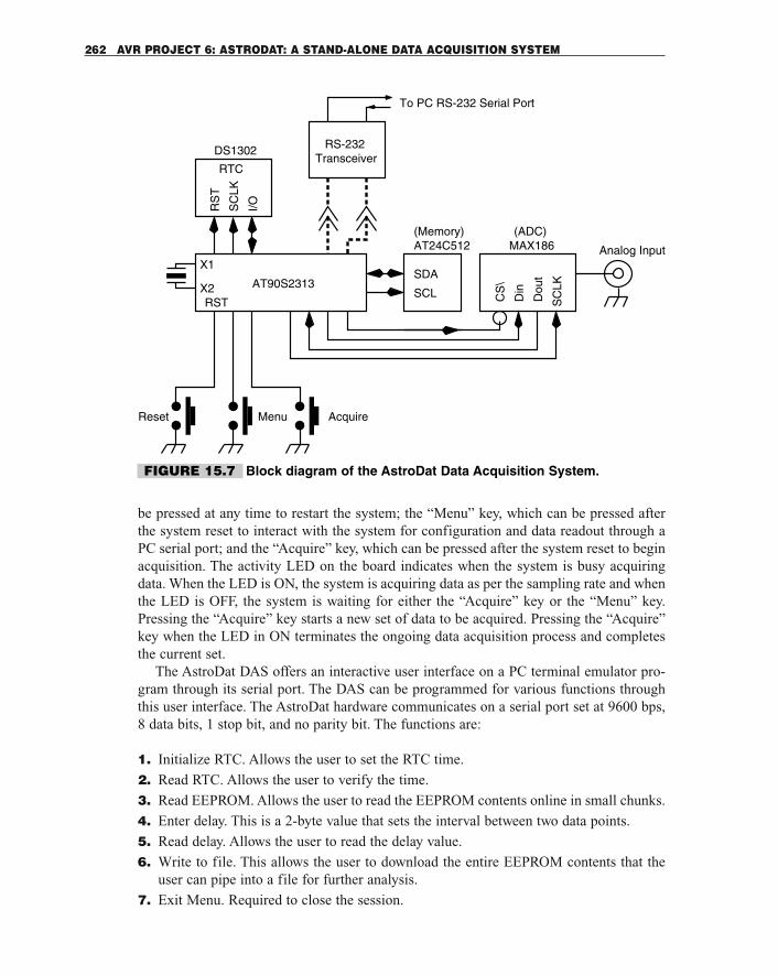
be pressed at any time to restart the system; the “Menu” key, which can be pressed afterthe system reset to interact with the system for configuration and data readout through aPC serial port; and the “Acquire” key, which can be pressed after the system reset to beginacquisition. The activity LED on the board indicates when the system is busy acquiringdata. When the LED is ON, the system is acquiring data as per the sampling rate and whenthe LED is OFF, the system is waiting for either the “Acquire” key or the “Menu” key.Pressing the “Acquire” key starts a new set of data to be acquired. Pressing the “Acquire”key when the LED in ON terminates the ongoing data acquisition process and completesthe current set.
The AstroDat DAS offers an interactive user interface on a PC terminal emulator pro-gram through its serial port. The DAS can be programmed for various functions throughthis user interface. The AstroDat hardware communicates on a serial port set at 9600 bps,8 data bits, 1 stop bit, and no parity bit. The functions are:
1. Initialize RTC. Allows the user to set the RTC time.
2. Read RTC. Allows the user to verify the time.
3. Read EEPROM. Allows the user to read the EEPROM contents online in small chunks.
4. Enter delay. This is a 2-byte value that sets the interval between two data points.
5. Read delay. Allows the user to read the delay value.
6. Write to file. This allows the user to download the entire EEPROM contents that theuser can pipe into a file for further analysis.
7. Exit Menu. Required to close the session.
262 AVR PROJECT 6: ASTRODAT: A STAND-ALONE DATA ACQUISITION SYSTEM
Analog Input
(Memory)AT24C512
CS
\
Din
Dou
t
MAX186(ADC)
SDA
SCL
RS
T
SC
LK
I/O
RS-232Transceiver
DS1302
RTC
AT90S2313
Reset
To PC RS-232 Serial Port
X1
X2RST
Menu Acquire
SC
LK
FIGURE 15.7 Block diagram of the AstroDat Data Acquisition System.
15.7 Design DescriptionFigure 15.7 illustrates the block diagram of the AstroDat Hardware. The hardware is fair-ly similar to the SniffStick, except for additional components such as the RTC and an extraswitch. Besides, the AstroDat communicates to a host on a serial port rather than theDocking port as in SniffStick. This is because the AstroDat Uses a bigger 20-pinAT90S2313 processor with built-in serial port.
Figure 15.8 is the circuit schematic for AstroDat. The system uses AT90S2313 at 3.58MHz. Any other frequency could be used as well. This particular processor was chosen keep-ing in mind the potential code size, the need for a built-in serial port, SRAM for storing vari-ables, and stack, as well as a 16-bit timer for generating interrupts at precise intervals.
The peripheral devices used are Maxim MAX186 ADC, Dallas DS1302 RTC, andAtmel AT24C512 EEPROM. All of these devices have a serial communication protocol.The EEPROM has an IIC interface while the ADC uses SPI link. The RTC uses a simplethree-wire serial protocol. Figures 15.9, 15.10, and 15.11 illustrate the signal activity onthe AVR processor connected to the three peripheral devices.
The 16-bit Timer1 is programmed to generate interrupts at 10-ms intervals. The Timer1ISR counts the number of interrupts, and when this count equals the required time, an ADCsample is acquired and the data is written into the EEPROM.
The data is written into the EEPROM such that the MSB is written at a lower addressand the LSB is written at the next (higher) address. All entries into the EEPROM are writ-ten as a 2-byte word.
The AstroDat also interfaces to two switches which we call “Acquire” and “Menu”keyswitches. The “Menu” key switch is sampled by the program while the “Acquire” keyis connected to the INT0 (PD2) signal of the processor. The INT0 is programmed so thata low level on the pin generates an interrupt. The INT0 ISR debounces the key bounce anddetermines what is to be done with the event. The “Acquire” key has been connected to aninterrupt pin so that the program will respond anytime the key is pressed, and there is noneed to monitor the key in a polled manner. The “Acquire” key is used to toggle the dataacquisition activity. If the “Acquire” key is pressed the first time, it starts the data acquisi-tion process and keeps going till the memory gets full or till the “Acquire” key is pressedagain. On the second occasion, the data acquisition process is terminated, and the currentdata set that is written into the EEPROM is terminated with an end tag corresponding tothe start tag. The processor then waits again for either the “Acquire” key or the “Menu”key to be pressed. If the “Acquire” key is pressed, a new data set is initiated by writing anew start tag, and data is acquired and stored in the EEPROM at the programmed rate. Ifthe “Menu” key is pressed instead, the program goes into a user menu mode and commu-nicates to the user though the serial port (a PC terminal is connected to the serial port forthis purpose).
When the processor is acquiring data, an LED connected to a PD6 bit called the“Activity” LED is put ON. When the system is waiting for one of the two keys to bepressed, the “Activity” LED is off.
The INT0 interrupt connected to the “Acquire” key is disabled when the system is inuser menu mode (after the “Menu” key has been pressed and till the user does not exit theuser menu).
DESIGN DESCRIPTION 263
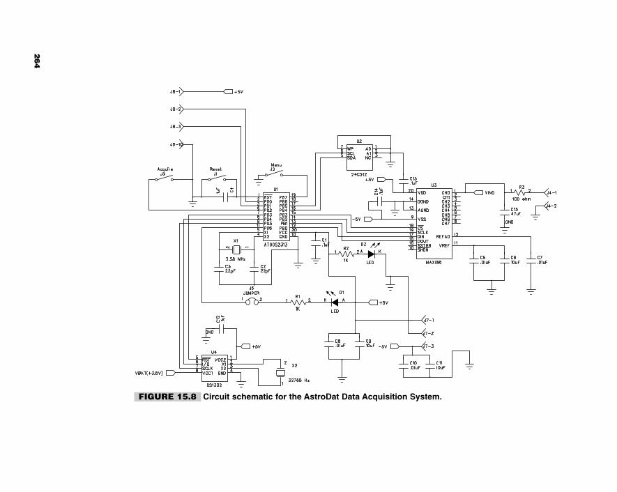
FIGURE 15.8 Circuit schematic for the AstroDat Data Acquisition System.
26
4
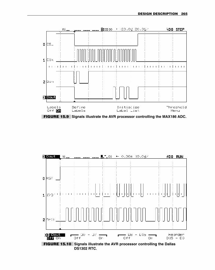
DESIGN DESCRIPTION 265
FIGURE 15.9 Signals illustrate the AVR processor controlling the MAX186 ADC.
FIGURE 15.10 Signals illustrate the AVR processor controlling the DallasDS1302 RTC.
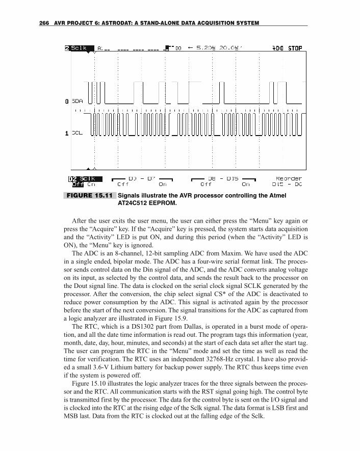
After the user exits the user menu, the user can either press the “Menu” key again orpress the “Acquire” key. If the “Acquire” key is pressed, the system starts data acquisitionand the “Activity” LED is put ON, and during this period (when the “Activity” LED isON), the “Menu” key is ignored.
The ADC is an 8-channel, 12-bit sampling ADC from Maxim. We have used the ADCin a single ended, bipolar mode. The ADC has a four-wire serial format link. The proces-sor sends control data on the Din signal of the ADC, and the ADC converts analog voltageon its input, as selected by the control data, and sends the result back to the processor onthe Dout signal line. The data is clocked on the serial clock signal SCLK generated by theprocessor. After the conversion, the chip select signal CS* of the ADC is deactivated toreduce power consumption by the ADC. This signal is activated again by the processorbefore the start of the next conversion. The signal transitions for the ADC as captured froma logic analyzer are illustrated in Figure 15.9.
The RTC, which is a DS1302 part from Dallas, is operated in a burst mode of opera-tion, and all the date time information is read out. The program tags this information (year,month, date, day, hour, minutes, and seconds) at the start of each data set after the start tag.The user can program the RTC in the “Menu” mode and set the time as well as read thetime for verification. The RTC uses an independent 32768-Hz crystal. I have also provid-ed a small 3.6-V Lithium battery for backup power supply. The RTC thus keeps time evenif the system is powered off.
Figure 15.10 illustrates the logic analyzer traces for the three signals between the proces-sor and the RTC. All communication starts with the RST signal going high. The control byteis transmitted first by the processor. The data for the control byte is sent on the I/O signal andis clocked into the RTC at the rising edge of the Sclk signal. The data format is LSB first andMSB last. Data from the RTC is clocked out at the falling edge of the Sclk.
266 AVR PROJECT 6: ASTRODAT: A STAND-ALONE DATA ACQUISITION SYSTEM
FIGURE 15.11 Signals illustrate the AVR processor controlling the AtmelAT24C512 EEPROM.
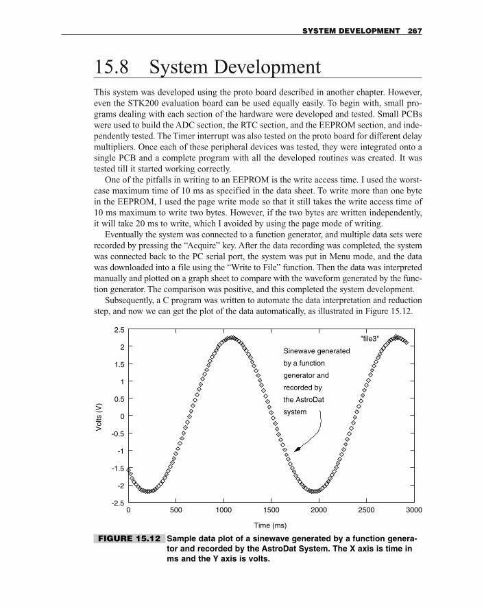
15.8 System DevelopmentThis system was developed using the proto board described in another chapter. However,even the STK200 evaluation board can be used equally easily. To begin with, small pro-grams dealing with each section of the hardware were developed and tested. Small PCBswere used to build the ADC section, the RTC section, and the EEPROM section, and inde-pendently tested. The Timer interrupt was also tested on the proto board for different delaymultipliers. Once each of these peripheral devices was tested, they were integrated onto asingle PCB and a complete program with all the developed routines was created. It wastested till it started working correctly.
One of the pitfalls in writing to an EEPROM is the write access time. I used the worst-case maximum time of 10 ms as specified in the data sheet. To write more than one bytein the EEPROM, I used the page write mode so that it still takes the write access time of10 ms maximum to write two bytes. However, if the two bytes are written independently,it will take 20 ms to write, which I avoided by using the page mode of writing.
Eventually the system was connected to a function generator, and multiple data sets wererecorded by pressing the “Acquire” key. After the data recording was completed, the systemwas connected back to the PC serial port, the system was put in Menu mode, and the datawas downloaded into a file using the “Write to File” function. Then the data was interpretedmanually and plotted on a graph sheet to compare with the waveform generated by the func-tion generator. The comparison was positive, and this completed the system development.
Subsequently, a C program was written to automate the data interpretation and reductionstep, and now we can get the plot of the data automatically, as illustrated in Figure 15.12.
SYSTEM DEVELOPMENT 267
-2.5
-2
-1.5
-1
-0.5
0
0.5
1
1.5
2
2.5
0 500 1000 1500 2000 2500 3000
"file3"
Time (ms)
Vol
ts (
V)
Sinewave generated
by a function
generator and
recorded by
the AstroDat
system
FIGURE 15.12 Sample data plot of a sinewave generated by a function genera-tor and recorded by the AstroDat System. The X axis is time inms and the Y axis is volts.
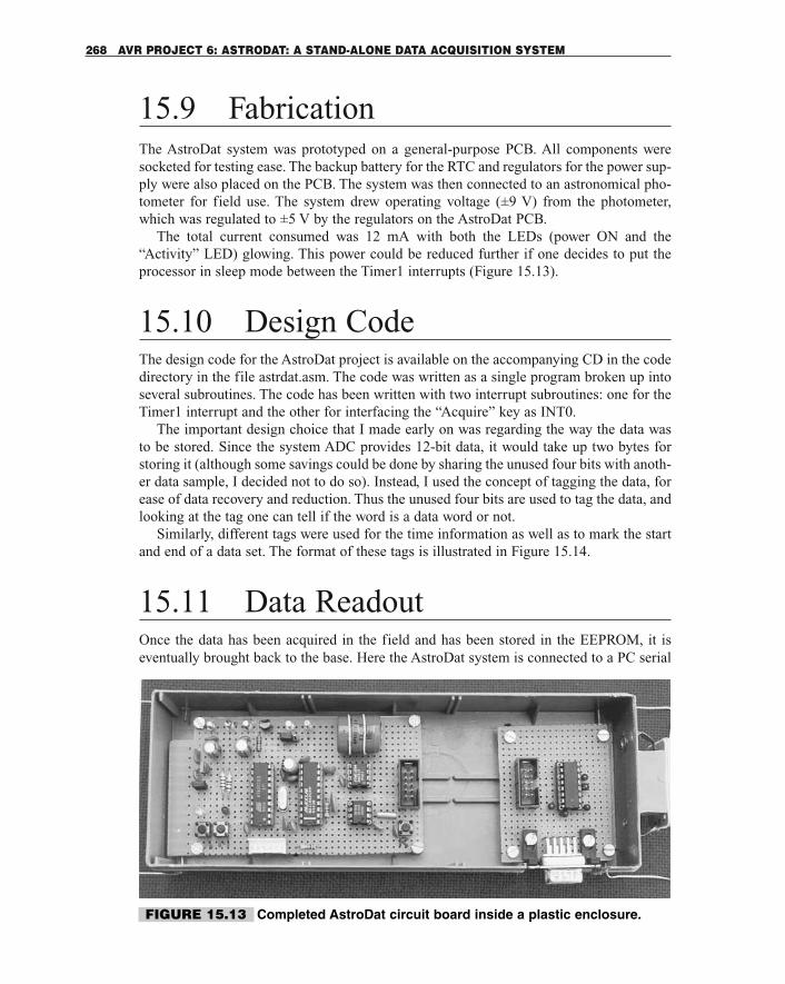
15.9 FabricationThe AstroDat system was prototyped on a general-purpose PCB. All components weresocketed for testing ease. The backup battery for the RTC and regulators for the power sup-ply were also placed on the PCB. The system was then connected to an astronomical pho-tometer for field use. The system drew operating voltage (±9 V) from the photometer,which was regulated to ±5 V by the regulators on the AstroDat PCB.
The total current consumed was 12 mA with both the LEDs (power ON and the“Activity” LED) glowing. This power could be reduced further if one decides to put theprocessor in sleep mode between the Timer1 interrupts (Figure 15.13).
15.10 Design CodeThe design code for the AstroDat project is available on the accompanying CD in the codedirectory in the file astrdat.asm. The code was written as a single program broken up intoseveral subroutines. The code has been written with two interrupt subroutines: one for theTimer1 interrupt and the other for interfacing the “Acquire” key as INT0.
The important design choice that I made early on was regarding the way the data wasto be stored. Since the system ADC provides 12-bit data, it would take up two bytes forstoring it (although some savings could be done by sharing the unused four bits with anoth-er data sample, I decided not to do so). Instead, I used the concept of tagging the data, forease of data recovery and reduction. Thus the unused four bits are used to tag the data, andlooking at the tag one can tell if the word is a data word or not.
Similarly, different tags were used for the time information as well as to mark the startand end of a data set. The format of these tags is illustrated in Figure 15.14.
15.11 Data ReadoutOnce the data has been acquired in the field and has been stored in the EEPROM, it iseventually brought back to the base. Here the AstroDat system is connected to a PC serial
268 AVR PROJECT 6: ASTRODAT: A STAND-ALONE DATA ACQUISITION SYSTEM
FIGURE 15.13 Completed AstroDat circuit board inside a plastic enclosure.
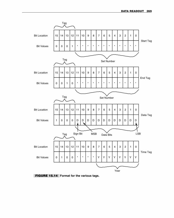
DATA READOUT 269
012356789101112131415 4
0 0 * * * * * * * * * * * *
Bit Location
Bit Values
012356789101112131415 4
0 0 0 1 * * * * * * * * * * * *
Bit Location
Bit Values
01
End Tag
Start Tag
012356789101112131415 4
0 0
Bit Location
Bit Values 01
012356789101112131415 4
0 * * * *
Bit Location
Bit Values 0
Time Tag
Data Tag
0 1
D D D D D D D D D D D D
Data Bits
Set Number
Set Number
Sign Bit MSB LSB
Y Y Y Y Y Y Y Y
Year
Tag
Tag
Tag
Tag
FIGURE 15.14 Format for the various tags.
port. A separate RS-232 to TTL converter PCB was built that connects to the communica-tion port of the AstroDat system at one end and the PC serial port on the other. This wasdone to minimize power consumption by the RS-232 signal translation components thatare not needed during the actual data acquisition process.
The EEPROM data is downloaded and stored into a file as described in the AstroDatUser’s Guide. The file is an ASCII file and can be inspected. However, I have written a Cprogram to read the file and recover the data for further analysis and plotting. One suchplot is illustrated in Figure 15.12.
15.12 AstroDat User’s GuideThe AstroDat system operates in two modes: Menu mode and Acquisition mode. TheMenu mode is selected when the user presses the “Menu” switch after reset. To operate thesystem in Menu mode, the AstroDat system is connected to a PC serial port running somesort of terminal emulation program, and the “Menu” key is pressed. The sequence in whichthe two keys can be pressed is illustrated in Figure 15.15. The data acquisition systemdesigned is used to store data from an analog source with time delay between two acquisi-tions being programmed by the user.
The device is first initialized by the user at the base. For this purpose, a “Menu’’ switchis provided. After the system has been initialized as required, it is taken to the field for dataacquisition. The data is stored as blocks; each block of data is called a set. The start and endof a set is controlled by the user by pressing the “acquire” switch. The data samples in a setare separated by a time delay, which is programmed by the user at the base. Also, the devicehas the capability to store the time at which the first observation in a set was recorded.
Data stored in the EEPROM has tags that help to interpret the data. Each set of observa-tions is identified by a unique “set number.” Each set of observations will have a start tag(containing the set number) in the beginning of the set and a stop tag indicating the end ofthe set. The actual data samples are identified by a data tag. Also, each start tag is followedby a time tag that indicates the time at which the first observation of the set was recorded.
System initialization The “Menu” switch is used for interaction between the systemand the user. It helps the user to initialize the real time clock (RTC), change the time inter-val (delay value) between two observations in a set, download data from the system, etc.To initialize the circuit, the following steps are to be followed:
1) Connect the port P1 to RS-232 board.2) Connect serial port of the PC to the RS-232 board.3) Connect power supply to the appropriate pins on the system board.4) Load VTERM (or any other terminal emulation program) on the computer.
The terminal is set up to communicate with the following features:i) New line—ONii) Wrap around—ONiii) Data bits—8
270 AVR PROJECT 6: ASTRODAT: A STAND-ALONE DATA ACQUISITION SYSTEM
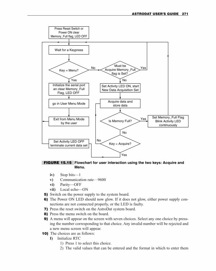
iv) Stop bits—1v) Communication rate—9600vi) Parity—OFFvii) Local echo—ON
5) Switch on the power supply to the system board.6) The Power ON LED should now glow. If it does not glow, either power supply con-
nections are not connected properly, or the LED is faulty.7) Press the reset switch on the AstroDat system board.8) Press the menu switch on the board.9) A menu will appear on the screen with seven choices. Select any one choice by press-
ing the number corresponding to that choice. Any invalid number will be rejected anda new menu screen will appear.
10) The choices are as follows:I) Initialize RTC
1) Press 1 to select this choice.2) The valid values that can be entered and the format in which to enter them
ASTRODAT USER’S GUIDE 271
Press Reset Switch orPower ON clear
Memory_Full flag, LED OFF
Initialize the serial portan clear Memory_Full
Flag, LED OFF
No
Yes
Wait for a Keypress
Set Activity LED ON, startNew Data Acquisition Set
Acquire data andstore data
Is Memory Full?
Set Activity LED OFFterminate current data set
Set Memory_Full FlagBlink Activity LED
continuously
Exit from Menu Modeby the user
go in User Menu Mode
Yes
No
Yes
No
Yes
No
Key = Menu?
Key = Acquire?
Must beAcquire Memory_Full
flag is Set?
FIGURE 15.15 Flowchart for user interaction using the two keys: Acquire andMenu.
will be displayed. Data should be entered in the proper format and shouldhave the correct values.
3) For example, if you wish to enter the following values: 3rd December, 1999,time is 15:01:23 and day is Friday, then enter data as follows:a) Enter 23b) Press space barc) Enter 01d) Press space bare) Enter 15f) Press space barg) Enter 03h) Press space bari) Enter 12j) Press space bark) Enter 05l) Press space barm) Enter 99
4) After the last value is entered, the main menu screen will appear.
Note: Day is chosen such that Monday is day 01 and Sunday is day 07. Time is taken in24-hour format. To enter 1, the user should enter 01. Single digits are invalid.
II) Read RTC1) Press 2 to select this choice.2) The choice will display the current data in the RTC.3) The format of each field in the data is displayed on the screen for interpretation.4) To go back to the main menu user should press a key.
III) Read EEPROM1) Press 3 to select this choice.2) The choice is used to read data stored in the EEPROM, in batches.3) At a given time, a certain amount of the data stored in the EEPROM is dis-
played. To view another batch of data, the user should press a key. Once allthe data stored in the EEPROM has been displayed, pressing of a key willdisplay the main menu again.
4) Displaying the data in batches helps the user to interpret the data as it is dis-played on the screen. Do not use this choice to store EEPROM data into a file.
5) Interpretation of the data stored is given afterwards.IV) Enter delay
1) Press 4 to select this choice.2) The choice is used to allow the user to change the value of delay time
between two observations in a set. The value of this delay is the same for allsets of data observations.
3) The delay value is calculated as follows:a) Divide the delay value required (in milliseconds) by 10.b) Convert the quotient obtained into hex.c) Enter the hex value obtained as the delay value.
4) After the delay value has been entered the main menu screen will appear.
272 AVR PROJECT 6: ASTRODAT: A STAND-ALONE DATA ACQUISITION SYSTEM
Note: The delay value entered should be of four digits always. The minimum value that canbe entered is 0002 and the maximum value that can be entered is FFFF.
V) Read delay1) Press 5 to select this choice.2) The choice is used to display the current delay value stored in the system.
Value is displayed in hex format.3. Conversion of the value displayed is as follows:
a) Convert the value displayed (in hex) to decimal.b) Multiply the decimal value by 10.c) The product obtained is the actual delay value in milliseconds.
4) User should press a key to return to the menu.V) Write to file
1) Press 6 to select this choice.2) The choice is used to display the data stored in the EEPROM without any
breakage. After the data is displayed, the user should press a key to return tothe main menu.
3) The choice can be used to store EEPROM data into a file for further pro-cessing. Before selecting this choice, appropriate file store/transfer com-mands should be set up in VTERM.
VII) Exit1) Press 7 to select this choice.2) The choice is used to exit from menu mode. On selecting this choice, the
screen should go blank.
Acquiring data in the field The “acquire” switch is used to indicate the start andend of a set of observations. Pressing the “acquire” switch when the “activity” LED isoff indicates the start of a set. The system now starts taking observations, and this isindicated by a glowing “activity” LED. The time delay between two data acquisitions ina set is programmed by the user, at the base using the “menu” switch. Pressing the“acquire” switch again will indicate the end of the set. The “activity” LED now switch-es off. The data thus recorded can be read back and analyzed at the base using the“menu” switch.
The following steps should be followed for acquiring data in the field:
1) Connect the power supply to the appropriate pins on the system board.2) Connect the analog input signal to be stored to the data pin (J4).3) Switch on the power supply to the system board.4) The “red” LED should now glow. If it does not glow, either power supply connections
are not connected properly, or the LED is faulty.5) Press the reset switch on the system board.6) Press the “acquire” switch to indicate the start of a set of observations. The “activity”
LED now glows.7) Press the “acquire” switch whenever the data acquisition for the set has to be stopped.
The “activity” LED will now switch off.8) Press the acquire switch whenever another set of observations has to be recorded.
ASTRODAT USER’S GUIDE 273
Note:1) The power supply, once switched on, should not be switched off even between two
sets of data acquisitions, when the system is not actually recording any data.Switching off the power will reset the circuit. When power is restored and the“acquire” switch is pressed again, the previous set of data acquisitions will be over-written. The same precaution should be taken with the “reset” switch. It should bepressed only once after the power supply is given to the circuit.
2) In the field, the “menu” switch should not be pressed at all. This switch should bepressed only when the system has to be initialized at the base. Pressing this switchin the field (when the system is not interfaced with a computer) will hang the sys-tem and it will have to be reset.
3) While the data acquisition is in progress, if the “activity” LED starts flickering, thenit indicates that the system memory (EEPROM memory) is full and no further sam-ples can be recorded. Pressing the “acquire” switch now will not affect the status ofthe “activity” LED and the system has to be reset.
Storing of data in the memory The data in the EEPROM (system memory) isstored as illustrated below. The format illustrated can be used for interpreting the data readfrom the EEPROM.
MEMORY LOCATION DATA STORED
0000–0001 Time delay value
0002–0003 Start tag � set number
0004–000B Time tag � time
000C–000D Data tag � data
. .
. .
. .
(n)–(n � 1) End tag � set number
(n � 2)–(n � 3) Start tag � set number
. .
. .
Definition of individual tags1) Start tag � set number
This tag is two bytes. Start tag is 1H (0001)b followed by the set number of 12 bits.
BIT NUMBER DATA STORED
15 0
14 0
13 0
12 1
11-0 Set number
274 AVR PROJECT 6: ASTRODAT: A STAND-ALONE DATA ACQUISITION SYSTEM
2) End tag � set numberThis tag is also two bytes. The set number in this tag is the same as that in the corre-sponding start tag. The stop tag is 2H (0010)b.
BIT NUMBER DATA STORED
15 0
14 0
13 1
12 0
11–0 Set number
3) Time tag � timeThe time tag is one byte which is followed by seven bytes of RTC data, which indicatesthe time at that the first observation in a set was recorded.
BYTE NUMBER DATA STORED
1 Time tag = 40H
2 Year value
3 Day value
4 Month value
5 Date value
6 Hour value
7 Minute Value
8 Seconds value
4) Data tag � dataThis tag is two bytes. The data tag is 8H, which is followed by 12 bits of actual sam-pled data.
BIT NUMBER DATA STORED
15 1
14 0
13 0
12 0
11–0 Sampled data value
The sampled data value is interpreted as follows: Bit11 is the sign. “1” indicates that the data value inbits 10–0 is in two’s complement and the sampled value isnegative. “0” indicates that the data value in bits 10–0 is to be read as it is, and the sam-
pled value is positive.
ASTRODAT USER’S GUIDE 275

This page intentionally left blank.
16.1 At a GlanceThis chapter looks at ways of building security locks, also called dongles, for variousapplications.
It covers:
1. What security locks are2. Some ways in which security locks can be designed3. The algorithm for such locks4. Building the locks for the serial or the parallel port of the PC5. Designing a novel security lock for the PC parallel port6. PC driver for the lock7. Alternate designs
16AVR PROJECT 7:
SECURITY DONGLE
277
Copyright 2001 The McGraw-Hill Companies, Inc. Click Here for Terms of Use.
16.2 Introduction16.2.1 WHAT ARE SECURITY LOCKS?
What are security locks and what are they used for? Security locks in the context of com-puter hardware and software refers to a system of authorization that allows use of suchhardware or software only to authorized users. As a computer user, you would be aware oflogin identification and associated password. Unless the correct password for a given loginidentification is entered, the computer system would not allow you to use the computer.This is an example of a software-based security lock of some sort.
Similarly, when you purchase some expensive software, the software author or the sup-plier would want some control over the use of the software only to authentic customers andwould like to restrict unauthorized proliferation of the software, as this leads to his loss ofrevenue. To implement this control, the author could provide you with a piece of hardwarethat is to be connected to the PC system on which the software is supposed to run. Whenyou run the software on a computer, it would look for the presence of this hardware and ifit fails to find it, the software would abort and terminate. On the contrary, when it findsthe hardware present in the system, the software performs merrily.
Typically, this additional piece of hardware is in the form of a small, sealed printed cir-cuit board with circuitry and with a means of connecting it to the host computer. To allowthe user to connect and disconnect this hardware easily, it is usually connected to the hostparallel port or the RS-232 serial port, as these are the ports that are easily accessible tothe user. Security locks to go on the USB also are available. The lock system works in thefollowing manner:
1. The PC software sends some information to the lock and expects some return infor-mation.
2. If the lock has been installed and is performing correctly, it would supply back theexpected information, in which case the software continues to execute.
3. If the lock has not been installed or has been removed, the software does not get whatit is looking for and so it aborts. Typically, the software periodically queries the lock.
16.2.2 VARIOUS HARDWARE LOCK SCHEMES
There could be many ways in which the software sends information to the lock andexpects the return information, and this distinguishes one lock from another. A goodlock should not only work as a deterrent against unauthorized proliferation, but shouldalso protect against any hacking attempt. This can be achieved if the lock scheme hasinfinite combinations (just like a mechanical lock). If a lock scheme always sends oneparticular type of information and expects a particular return answer, it is no good, as
278 AVR PROJECT 7: SECURITY DONGLE
this can be duplicated. Ideally, the lock should have infinite combinations, though inpractice that may not be feasible.
A good portable hardware lock system should offer the following features:
1. Should connect to user ports such as the parallel port or the RS-232 port.2. Should derive power for the lock circuit out of these ports.3. Should have a large number of combinations so as to resist any duplication attempts.4. For the parallel-port-based locks, should offer a pass-through parallel port; i.e., the user
should be able to connect other peripherals to the parallel port apart from the lock.5. Application software should periodically detect the presence of the lock by communi-
cating with it.
Figure 16.1 shows a security lock connected on the PC RS-232 serial port. This figureillustrates the circuitry to contain an AT90S2343 processor to indicate that, in principle,the lock could be implemented using this processor. The RS-232 port signals are used notonly for communicating with the lock, but are also used to power the lock. The signals onthe RS-232 port have �12-V or �12-V voltages. The application software (which employsthe lock) should drive these signals (DTR and RTS in the figure) to �12 V, which is thenstepped down to a suitable level for the purpose of powering the lock. The other signalsillustrated, TxD, and the RxD, are transmit and receive data signals and can be used by thelock to receive and transmit data respectively.
This establishes a basic infrastructure on which a given lock algorithm could be based.Of course, it is assumed that the circuit employed would support the needs of the lock algorithm.
Another way to design the security lock on the PC parallel port is illustrated in Figure16.2. This scheme is slightly more demanding than the RS-232 port. This is because usu-ally a PC would have only a single parallel port, the use of which cannot be given up(printing, etc.) simply because you want to use it for a hardware lock! To alleviate this pos-sible problem, people have come up with a concept called a pass-through parallel port,which essentially means that the parallel port is a shared resource among many peripher-als. In my laboratory, a single parallel port is used to connect to a ZIP drive, an HPprinter, and a PADS application software hardware lock, all working in quiet harmony.
INTRODUCTION 279
+5VDTR
RTS
TxD
RxD
RS-232
Voltage
Regulator
AT90S2343
+Vcc
FIGURE 16.1 A security lock on the RS-232 port of the PC.
The ZIP drive is connected first to the parallel port. The hardware lock goes on the pass-through port of the ZIP drive and the printer is attached to the pass-through port of thelock! So this means that the lock circuit in a parallel-port-based lock has to be extra smartcompared to that in the RS-232-based lock.
16.3 How to Build an Electronic LockNow that we have covered the basics of electronic hardware lock requirements, let us seewhat it takes to build an electronic hardware lock. We have seen that the lock has a schemethat we call the lock algorithm. Then it must be possible to put that algorithm in the formof realizable hardware. Next, it must connect to one of the user ports for ease of operation.It must derive power from the port. It must use the port for communication with the appli-cation software (the software that is supposed to employ the lock) and most of all, the lockmust offer pass-through capability.
If we want to build a lock, we must have the lock algorithm. There are many possiblelock schemes, from the very elementary to the very complex. An elementary, rather sillyscheme (though of equal deterrence) could be a simple wire link from an output signal lineof the PC port to an input signal line of the PC port. For the RS-232 port, that would meanshorting the TxD line to the RxD line. Whatever the PC transmits on the TxD line isreceived back by the PC on the RxD line.
A level of complexity could be built into this scheme by delaying the signal back to thePC by using some kind of memory element. The lock receives the data byte and tem-porarily stores the byte before transmitting it back on the RxD line. The next level of com-plexity could be incorporated by employing more memory elements that store a sequenceof data bytes received by the lock and then transmitting back in some sequence.
280 AVR PROJECT 7: SECURITY DONGLE
Parallel Port
AT90S2343
25 p
in ‘D
’ typ
e M
ale
Con
nect
or
Control Port
Data Port
Status Port
Pass-through
Port
25 p
in ‘D
’ typ
e fe
mal
e co
nnec
tor
FIGURE 16.2 A security lock on the PC parallel port with a pass-through port.
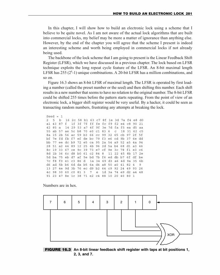
In this chapter, I will show how to build an electronic lock using a scheme that Ibelieve to be quite novel. As I am not aware of the actual lock algorithms that are builtinto commercial locks, my belief may be more a matter of ignorance than anything else.However, by the end of the chapter you will agree that the scheme I present is indeed an interesting scheme and worth being employed in commercial locks if not alreadybeing used.
The backbone of the lock scheme that I am going to present is the Linear Feedback ShiftRegister (LFSR), which we have discussed in a previous chapter. The lock based on LFSRtechnique exploits the long repeat cycle feature of the LFSR. An 8-bit maximal lengthLFSR has 255 (28-1) unique combinations. A 20-bit LFSR has a million combinations, andso on.
Figure 16.3 shows an 8-bit LFSR of maximal length. The LFSR is operated by first load-ing a number (called the preset number or the seed) and then shifting this number. Each shiftresults in a new number that seems to have no relation to the original number. The 8-bit LFSRcould be shifted 255 times before the pattern starts repeating. From the point of view of anelectronic lock, a bigger shift register would be very useful. By a hacker, it could be seen astransacting random numbers, frustrating any attempts at breaking the lock.
Seed = 12 5 b 16 2c 58 b1 63 c7 8f 1e 3d 7a f4 e8 d0a1 43 87 f 1f 3f 7f ff fe fc f9 f2 e4 c8 90 2142 85 a 14 29 53 a7 4f 9f 3e 7d fa f5 ea d5 aa55 ab 57 ae 5c b8 70 e0 c1 83 6 c 18 31 62 c58a 15 2b 56 ac 59 b3 66 cc 99 32 65 cb 97 2f 5fbf 7e fd fb f7 ef de bc 79 f3 e6 cd 9b 37 6e ddbb 77 ee dc b9 72 e5 ca 95 2a 54 a9 52 a5 4a 9428 51 a2 44 89 12 25 4b 96 2d 5a b4 68 d1 a3 468c 19 33 67 ce 9c 39 73 e7 cf 9e 3c 78 f1 e3 c68d 1b 36 6c d8 b0 61 c2 84 8 11 22 45 8b 17 2e5d ba 75 eb d7 af 5e bd 7b f6 ed db b7 6f df be7c f8 f0 e1 c3 86 d 1a 34 69 d3 a6 4d 9a 35 6bd6 ad 5b b6 6d da b5 6a d4 a8 50 a0 41 82 4 913 27 4e 9d 3b 76 ec d9 b2 64 c9 92 24 49 93 264c 98 30 60 c0 81 3 7 e 1d 3a 74 e9 d2 a4 4891 23 47 8e 1c 38 71 e2 c4 88 10 20 40 80 1
Numbers are in hex.
HOW TO BUILD AN ELECTRONIC LOCK 281
7 6 5 4 3 2 1 0
XOR
FIGURE 16.3 An 8-bit linear feedback shift register with taps at bit positions 1,2, 3, and 7.
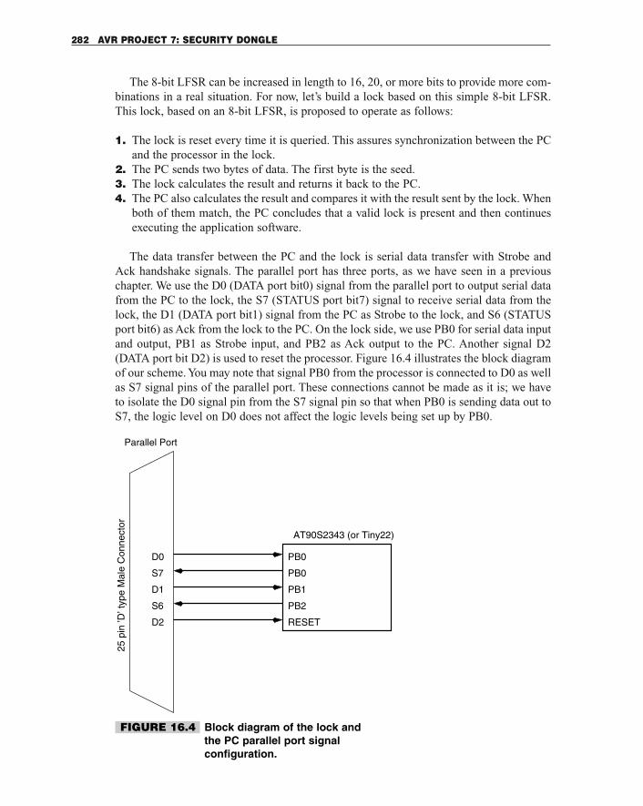
The 8-bit LFSR can be increased in length to 16, 20, or more bits to provide more com-binations in a real situation. For now, let’s build a lock based on this simple 8-bit LFSR.This lock, based on an 8-bit LFSR, is proposed to operate as follows:
1. The lock is reset every time it is queried. This assures synchronization between the PCand the processor in the lock.
2. The PC sends two bytes of data. The first byte is the seed.3. The lock calculates the result and returns it back to the PC.4. The PC also calculates the result and compares it with the result sent by the lock. When
both of them match, the PC concludes that a valid lock is present and then continuesexecuting the application software.
The data transfer between the PC and the lock is serial data transfer with Strobe andAck handshake signals. The parallel port has three ports, as we have seen in a previouschapter. We use the D0 (DATA port bit0) signal from the parallel port to output serial datafrom the PC to the lock, the S7 (STATUS port bit7) signal to receive serial data from thelock, the D1 (DATA port bit1) signal from the PC as Strobe to the lock, and S6 (STATUSport bit6) as Ack from the lock to the PC. On the lock side, we use PB0 for serial data inputand output, PB1 as Strobe input, and PB2 as Ack output to the PC. Another signal D2(DATA port bit D2) is used to reset the processor. Figure 16.4 illustrates the block diagramof our scheme. You may note that signal PB0 from the processor is connected to D0 as wellas S7 signal pins of the parallel port. These connections cannot be made as it is; we haveto isolate the D0 signal pin from the S7 signal pin so that when PB0 is sending data out toS7, the logic level on D0 does not affect the logic levels being set up by PB0.
282 AVR PROJECT 7: SECURITY DONGLE
Parallel Port
PB0
PB1
PB2
RESET
PB0
25 p
in ’D
’ typ
e M
ale
Con
nect
or
D0
S7
D1
S6
D2
AT90S2343 (or Tiny22)
FIGURE 16.4 Block diagram of the lock and the PC parallel port signal configuration.
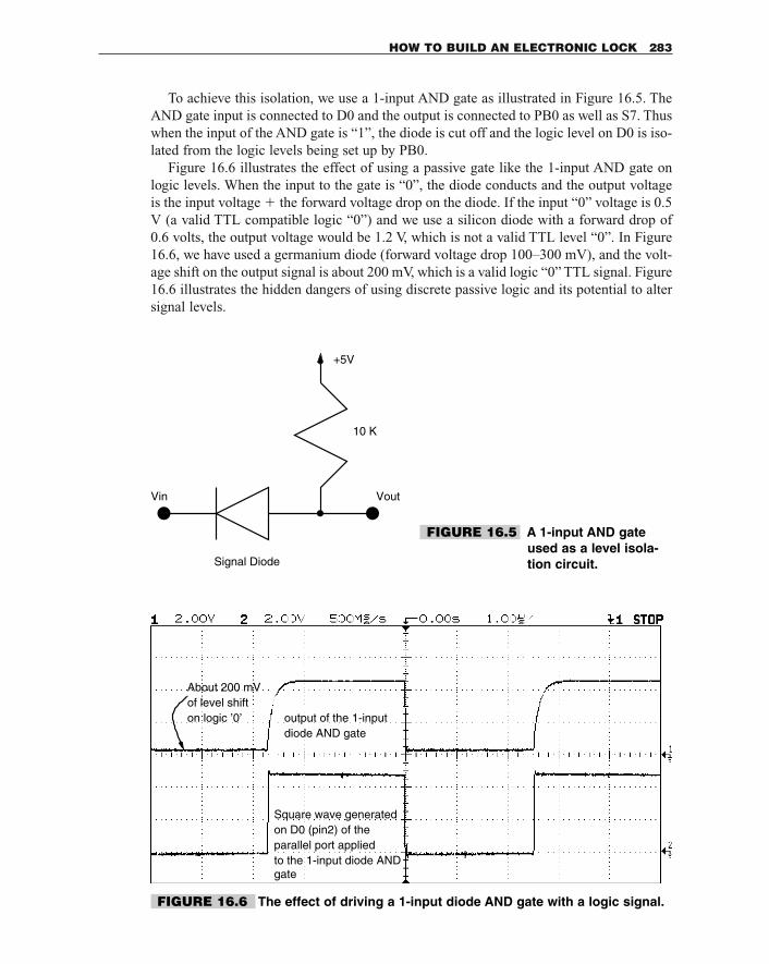
To achieve this isolation, we use a 1-input AND gate as illustrated in Figure 16.5. TheAND gate input is connected to D0 and the output is connected to PB0 as well as S7. Thuswhen the input of the AND gate is “1”, the diode is cut off and the logic level on D0 is iso-lated from the logic levels being set up by PB0.
Figure 16.6 illustrates the effect of using a passive gate like the 1-input AND gate onlogic levels. When the input to the gate is “0”, the diode conducts and the output voltageis the input voltage � the forward voltage drop on the diode. If the input “0” voltage is 0.5V (a valid TTL compatible logic “0”) and we use a silicon diode with a forward drop of0.6 volts, the output voltage would be 1.2 V, which is not a valid TTL level “0”. In Figure16.6, we have used a germanium diode (forward voltage drop 100–300 mV), and the volt-age shift on the output signal is about 200 mV, which is a valid logic “0” TTL signal. Figure16.6 illustrates the hidden dangers of using discrete passive logic and its potential to altersignal levels.
HOW TO BUILD AN ELECTRONIC LOCK 283
10 K
Signal Diode
+5V
VoutVin
FIGURE 16.5 A 1-input AND gateused as a level isola-tion circuit.
Square wave generatedon D0 (pin2) of theparallel port applied
output of the 1-inputdiode AND gate
to the 1-input diode ANDgate
About 200 mVof level shifton logic ’0’
FIGURE 16.6 The effect of driving a 1-input diode AND gate with a logic signal.
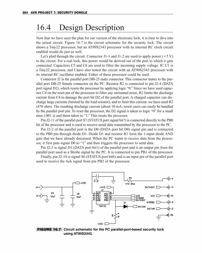
16.4 Design DescriptionNow that we have seen the plan for our version of the electronic lock, it is time to dive intothe actual circuit. Figure 16.7 is the circuit schematic for the security lock. The circuitshows a Tiny22 processor, but an AT90S2343 processor with its internal RC clock circuitenabled would do just as well.
Let’s plod through the circuit. Connector J1-1 and J1-2 are used to apply power (�5 V)to the circuit. For a real lock, this power would be derived out of the port to which it getsconnected. Capacitors C5 and C6 are used to filter the incoming supply voltage. IC U1 isa Tiny22 processor, and I have also tested the circuit with an AT90S2343 processor withits internal RC oscillator enabled. Either of these processor could be used.
Connector J2 is the parallel port DB-25 male connector. This connector mates to the par-allel port DB-25 female connector on the PC. Resistor R2 is connected to pin J2-4 (DATAport signal D2), which resets the processor by applying logic “0.” Since we have used capac-itor C4 on the reset pin of the processor to filter any unwanted noise, R2 limits the dischargecurrent from C4 to damage the port bit D2 of the parallel port. A charged capacitor can dis-charge large currents (limited by the load resistor), and to limit this current, we have used R2(470 ohm). The resulting discharge current (about 10 mA, worst case) can easily be handledby the parallel port pin. To reset the processor, the D2 signal is taken to logic “0” for a smalltime (.001 s) and them taken to “1.” This resets the processor.
Pin J2-11 of the parallel port S7 (STATUS port signal bit7) is connected directly to the PB0bit of the processor and is used to receive serial data transmitted by the processor to the PC.
Pin J2-2 of the parallel port is the D0 (DATA port bit D0) signal pin and is connectedto the PB0 pin through diode D1. Diode D1 and resistor R1 form the 1-input diode ANDgate that we have already discussed. When the PC wants to receive data from the proces-sor, it first puts signal D0 to “1” and then triggers the processor to send data.
Pin J2-3 is signal D1 (DATA port bit1) of the parallel port and is an output pin from theparallel port used as a Strobe signal by the PC. It is connected to pin PB1 of the processor.
Finally, pin J2-10 is signal S6 (STATUS port bit6) and is an input pin of the parallel portused to receive the Ack signal from pin PB2 of the processor.
284 AVR PROJECT 7: SECURITY DONGLE
FIGURE 16.7 Circuit schematic for the PC parallel-port-based security lockusing AT90S2343.
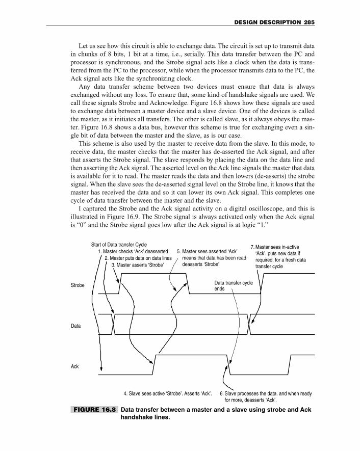
Let us see how this circuit is able to exchange data. The circuit is set up to transmit datain chunks of 8 bits, 1 bit at a time, i.e., serially. This data transfer between the PC andprocessor is synchronous, and the Strobe signal acts like a clock when the data is trans-ferred from the PC to the processor, while when the processor transmits data to the PC, theAck signal acts like the synchronizing clock.
Any data transfer scheme between two devices must ensure that data is alwaysexchanged without any loss. To ensure that, some kind of handshake signals are used. Wecall these signals Strobe and Acknowledge. Figure 16.8 shows how these signals are usedto exchange data between a master device and a slave device. One of the devices is calledthe master, as it initiates all transfers. The other is called slave, as it always obeys the mas-ter. Figure 16.8 shows a data bus, however this scheme is true for exchanging even a sin-gle bit of data between the master and the slave, as is our case.
This scheme is also used by the master to receive data from the slave. In this mode, toreceive data, the master checks that the master has de-asserted the Ack signal, and afterthat asserts the Strobe signal. The slave responds by placing the data on the data line andthen asserting the Ack signal. The asserted level on the Ack line signals the master that datais available for it to read. The master reads the data and then lowers (de-asserts) the strobesignal. When the slave sees the de-asserted signal level on the Strobe line, it knows that themaster has received the data and so it can lower its own Ack signal. This completes onecycle of data transfer between the master and the slave.
I captured the Strobe and the Ack signal activity on a digital oscilloscope, and this isillustrated in Figure 16.9. The Strobe signal is always activated only when the Ack signalis “0” and the Strobe signal goes low after the Ack signal is at logic “1.”
DESIGN DESCRIPTION 285
1. Master checks ‘Ack’ deasserted2. Master puts data on data lines
3. Master asserts ‘Strobe’
4. Slave sees active ‘Strobe’. Asserts ‘Ack’.
5. Master sees asserted ‘Ack’means that data has been readdeasserts ‘Strobe’
6. Slave processes the data. and when readyfor more, deasserts ‘Ack’.
7. Master sees in-active‘Ack’. puts new data ifrequired, for a fresh datatransfer cycle
Start of Data transfer Cycle
Data transfer cycleends
Strobe
Data
Ack
FIGURE 16.8 Data transfer between a master and a slave using strobe and Ackhandshake lines.
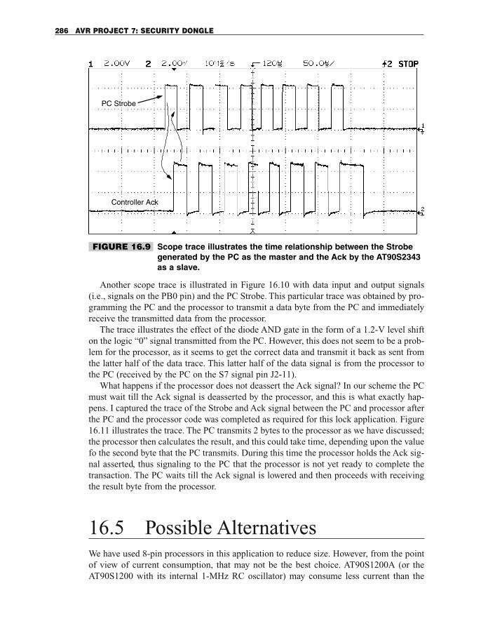
Another scope trace is illustrated in Figure 16.10 with data input and output signals(i.e., signals on the PB0 pin) and the PC Strobe. This particular trace was obtained by pro-gramming the PC and the processor to transmit a data byte from the PC and immediatelyreceive the transmitted data from the processor.
The trace illustrates the effect of the diode AND gate in the form of a 1.2-V level shifton the logic “0” signal transmitted from the PC. However, this does not seem to be a prob-lem for the processor, as it seems to get the correct data and transmit it back as sent fromthe latter half of the data trace. This latter half of the data signal is from the processor tothe PC (received by the PC on the S7 signal pin J2-11).
What happens if the processor does not deassert the Ack signal? In our scheme the PCmust wait till the Ack signal is deasserted by the processor, and this is what exactly hap-pens. I captured the trace of the Strobe and Ack signal between the PC and processor afterthe PC and the processor code was completed as required for this lock application. Figure16.11 illustrates the trace. The PC transmits 2 bytes to the processor as we have discussed;the processor then calculates the result, and this could take time, depending upon the valuefo the second byte that the PC transmits. During this time the processor holds the Ack sig-nal asserted, thus signaling to the PC that the processor is not yet ready to complete thetransaction. The PC waits till the Ack signal is lowered and then proceeds with receivingthe result byte from the processor.
16.5 Possible AlternativesWe have used 8-pin processors in this application to reduce size. However, from the pointof view of current consumption, that may not be the best choice. AT90S1200A (or theAT90S1200 with its internal 1-MHz RC oscillator) may consume less current than the
286 AVR PROJECT 7: SECURITY DONGLE
PC Strobe
Controller Ack
FIGURE 16.9 Scope trace illustrates the time relationship between the Strobegenerated by the PC as the master and the Ack by the AT90S2343as a slave.
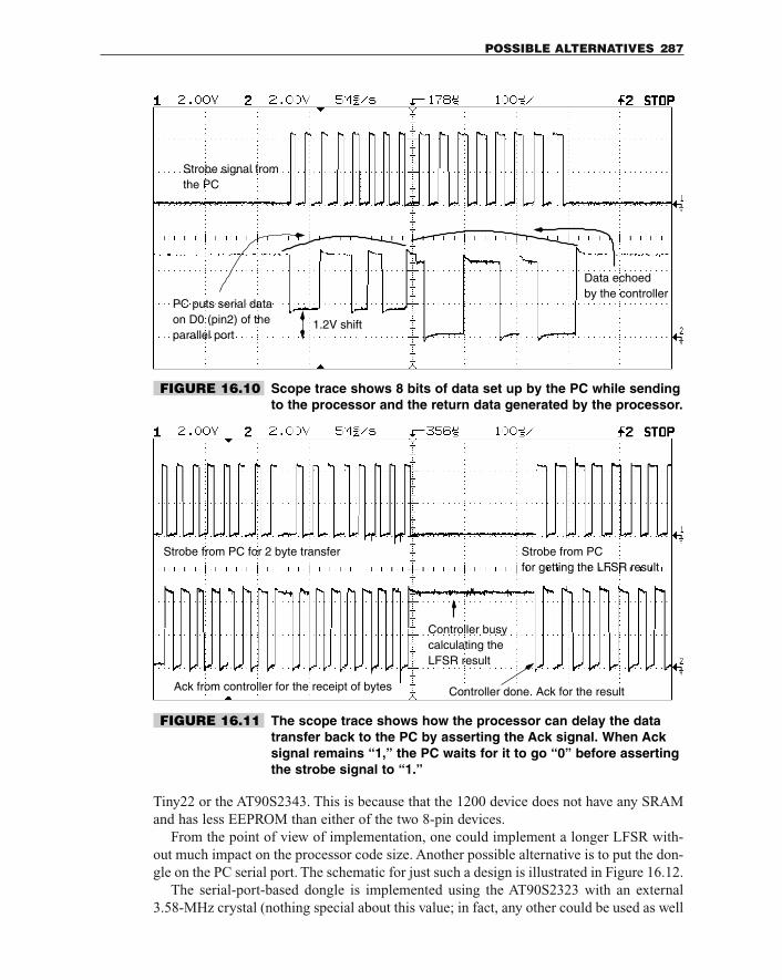
Tiny22 or the AT90S2343. This is because that the 1200 device does not have any SRAMand has less EEPROM than either of the two 8-pin devices.
From the point of view of implementation, one could implement a longer LFSR with-out much impact on the processor code size. Another possible alternative is to put the don-gle on the PC serial port. The schematic for just such a design is illustrated in Figure 16.12.
The serial-port-based dongle is implemented using the AT90S2323 with an external3.58-MHz crystal (nothing special about this value; in fact, any other could be used as well
POSSIBLE ALTERNATIVES 287
PC puts serial dataon D0 (pin2) of theparallel port
Strobe signal fromthe PC
Data echoedby the controller
1.2V shift
FIGURE 16.10 Scope trace shows 8 bits of data set up by the PC while sendingto the processor and the return data generated by the processor.
Strobe from PC for 2 byte transfer
Ack from controller for the receipt of bytes
Controller busycalculating theLFSR result
Strobe from PCfor getting the LFSR result
Controller done. Ack for the result
FIGURE 16.11 The scope trace shows how the processor can delay the datatransfer back to the PC by asserting the Ack signal. When Acksignal remains “1,” the PC waits for it to go “0” before assertingthe strobe signal to “1.”
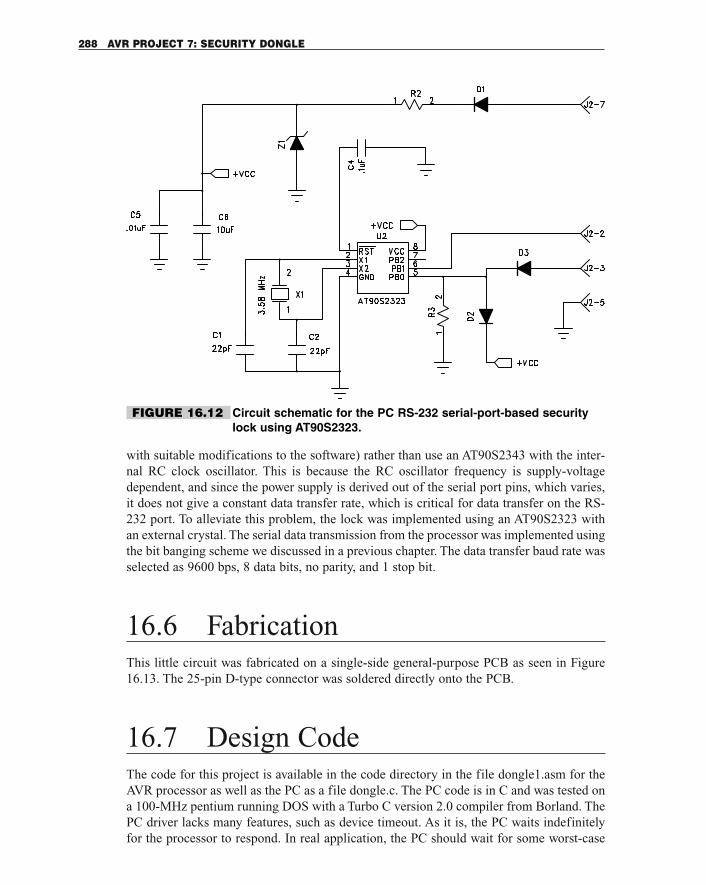
with suitable modifications to the software) rather than use an AT90S2343 with the inter-nal RC clock oscillator. This is because the RC oscillator frequency is supply-voltagedependent, and since the power supply is derived out of the serial port pins, which varies,it does not give a constant data transfer rate, which is critical for data transfer on the RS-232 port. To alleviate this problem, the lock was implemented using an AT90S2323 withan external crystal. The serial data transmission from the processor was implemented usingthe bit banging scheme we discussed in a previous chapter. The data transfer baud rate wasselected as 9600 bps, 8 data bits, no parity, and 1 stop bit.
16.6 FabricationThis little circuit was fabricated on a single-side general-purpose PCB as seen in Figure16.13. The 25-pin D-type connector was soldered directly onto the PCB.
16.7 Design CodeThe code for this project is available in the code directory in the file dongle1.asm for theAVR processor as well as the PC as a file dongle.c. The PC code is in C and was tested ona 100-MHz pentium running DOS with a Turbo C version 2.0 compiler from Borland. ThePC driver lacks many features, such as device timeout. As it is, the PC waits indefinitelyfor the processor to respond. In real application, the PC should wait for some worst-case
288 AVR PROJECT 7: SECURITY DONGLE
FIGURE 16.12 Circuit schematic for the PC RS-232 serial-port-based securitylock using AT90S2323.
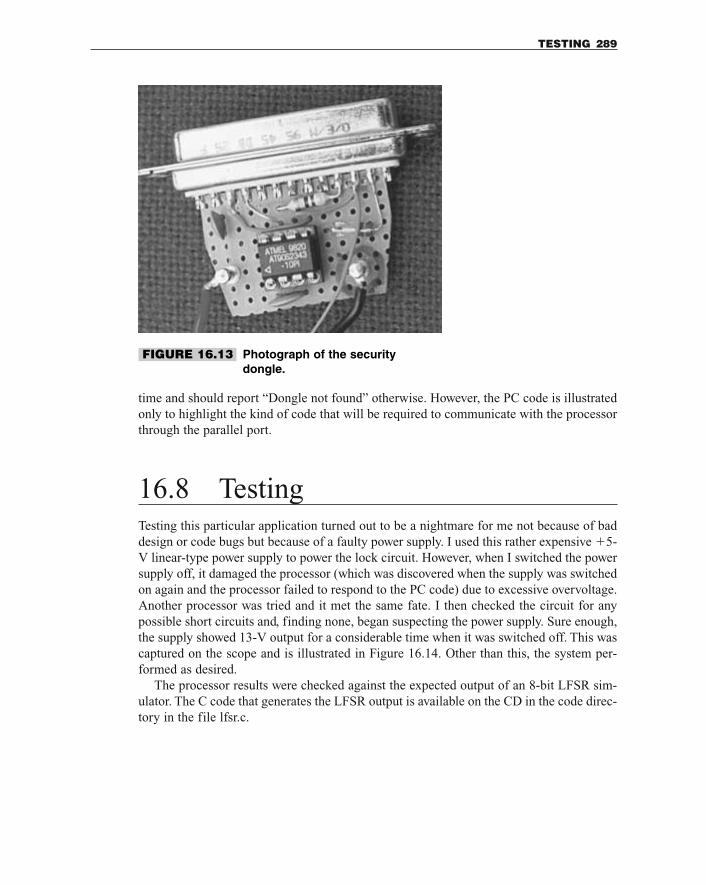
time and should report “Dongle not found” otherwise. However, the PC code is illustratedonly to highlight the kind of code that will be required to communicate with the processorthrough the parallel port.
16.8 TestingTesting this particular application turned out to be a nightmare for me not because of baddesign or code bugs but because of a faulty power supply. I used this rather expensive �5-V linear-type power supply to power the lock circuit. However, when I switched the powersupply off, it damaged the processor (which was discovered when the supply was switchedon again and the processor failed to respond to the PC code) due to excessive overvoltage.Another processor was tried and it met the same fate. I then checked the circuit for anypossible short circuits and, finding none, began suspecting the power supply. Sure enough,the supply showed 13-V output for a considerable time when it was switched off. This wascaptured on the scope and is illustrated in Figure 16.14. Other than this, the system per-formed as desired.
The processor results were checked against the expected output of an 8-bit LFSR sim-ulator. The C code that generates the LFSR output is available on the CD in the code direc-tory in the file lfsr.c.
TESTING 289
FIGURE 16.13 Photograph of the security dongle.
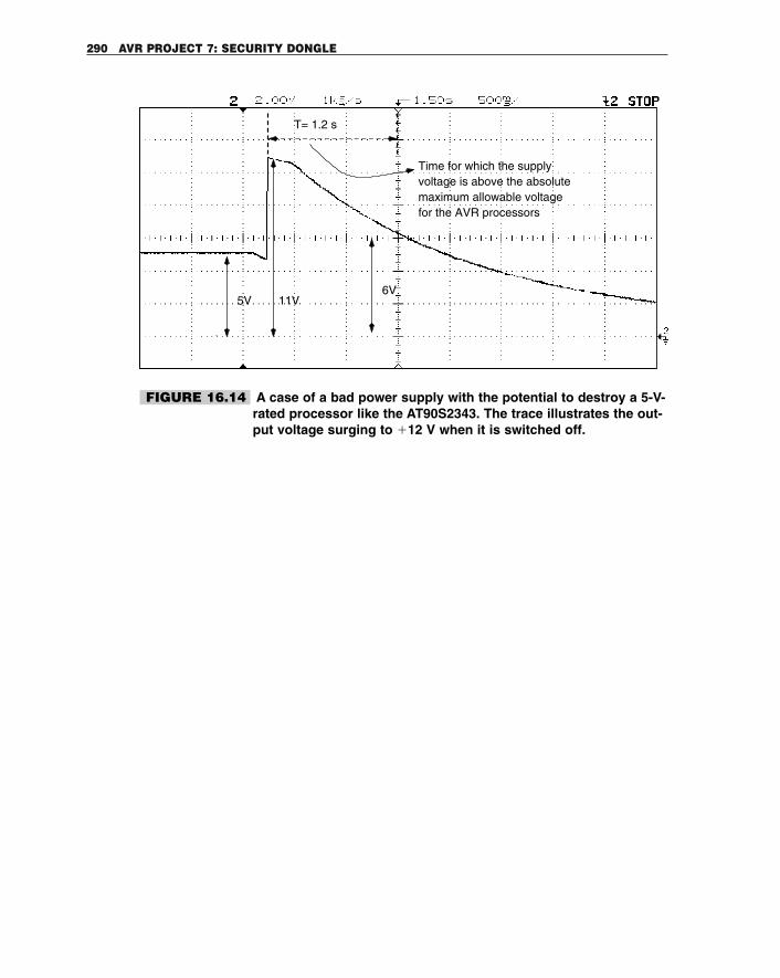
290 AVR PROJECT 7: SECURITY DONGLE
5V 11V
Time for which the supplyvoltage is above the absolutemaximum allowable voltagefor the AVR processors
T= 1.2 s
6V
FIGURE 16.14 A case of a bad power supply with the potential to destroy a 5-V-rated processor like the AT90S2343. The trace illustrates the out-put voltage surging to �12 V when it is switched off.
17.1 At a GlanceIn this chapter we look at:
1. What a frequency/period counter is2. Design of a frequency counter3. Design of a period counter4. A working design of an AT90S2323-based frequency counter for the PC RS-232 ser-
ial port5. A practical application for the frequency counter
17.2 IntroductionMeasuring frequency can be a frequent requirement. You often need a frequency countereither as a general-purpose test instrument or as a gadget for a specific application. Witha general-purpose test instrument, you may want to measure the frequency of a signal, andwith a gadget you may want to measure the number of people passing a gate in a minute,
17AVR PROJECT 8: A PULSE
FREQUENCY COUNTER WITH
AN RS-232 INTERFACE
291
Copyright 2001 The McGraw-Hill Companies, Inc. Click Here for Terms of Use.
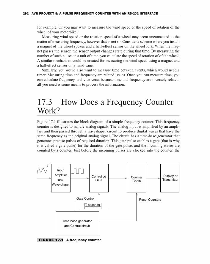
for example. Or you may want to measure the wind speed or the speed of rotation of thewheel of your motorbike.
Measuring wind speed or the rotation speed of a wheel may seem unconnected to thematter of measuring frequency, however that is not so. Consider a scheme where you installa magnet of the wheel spokes and a hall-effect sensor on the wheel fork. When the mag-net passes the sensor, the sensor output changes state during that time. By measuring thenumber of such pulses in a unit of time, you calculate the speed of rotation of of the wheel.A similar mechanism could be created for measuring the wind speed using a magnet anda hall-effect sensor on a wind vane.
Similarly, you would also want to measure time between events, which would need atimer. Measuring time and frequency are related issues. Once you can measure time, youcan calculate frequency, and vice-versa because time and frequency are inversely related;all you need is some means to process the information.
17.3 How Does a Frequency CounterWork?Figure 17.1 illustrates the block diagram of a simple frequency counter. This frequencycounter is designed to handle analog signals. The analog input is amplified by an ampli-fier and then passed through a waveshaper circuit to produce digital waves that have thesame frequency as the original analog signal. The circuit has a time-base generator thatgenerates precise pulses of required duration. This gate pulse enables a gate (that is whyit is called a gate pulse) for the duration of the gate pulse, and the incoming waves arecounted by a counter. Just before the incoming pulses are clocked into the counter, the
292 AVR PROJECT 8: A PULSE FREQUENCY COUNTER WITH AN RS-232 INTERFACE
GateControlled
ChainCounter Display or
Transmitter
Reset CountersGate Control
T seconds
Time-base generator
and Control circuit
Input
Amplifier
and
Wave shaper
FIGURE 17.1 A frequency counter.
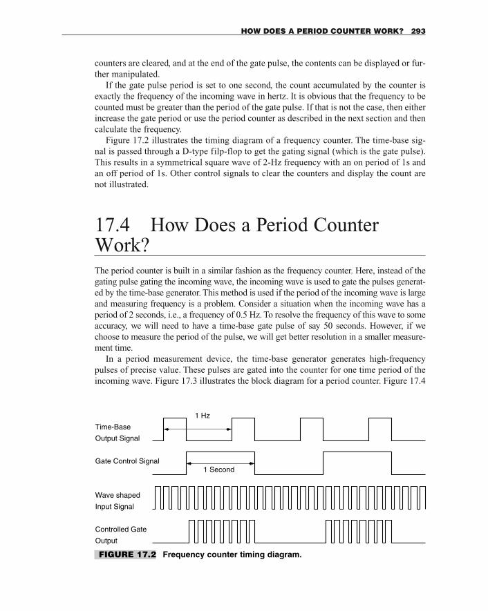
counters are cleared, and at the end of the gate pulse, the contents can be displayed or fur-ther manipulated.
If the gate pulse period is set to one second, the count accumulated by the counter isexactly the frequency of the incoming wave in hertz. It is obvious that the frequency to becounted must be greater than the period of the gate pulse. If that is not the case, then eitherincrease the gate period or use the period counter as described in the next section and thencalculate the frequency.
Figure 17.2 illustrates the timing diagram of a frequency counter. The time-base sig-nal is passed through a D-type filp-flop to get the gating signal (which is the gate pulse).This results in a symmetrical square wave of 2-Hz frequency with an on period of 1s andan off period of 1s. Other control signals to clear the counters and display the count arenot illustrated.
17.4 How Does a Period CounterWork?The period counter is built in a similar fashion as the frequency counter. Here, instead of thegating pulse gating the incoming wave, the incoming wave is used to gate the pulses generat-ed by the time-base generator. This method is used if the period of the incoming wave is largeand measuring frequency is a problem. Consider a situation when the incoming wave has aperiod of 2 seconds, i.e., a frequency of 0.5 Hz. To resolve the frequency of this wave to someaccuracy, we will need to have a time-base gate pulse of say 50 seconds. However, if wechoose to measure the period of the pulse, we will get better resolution in a smaller measure-ment time.
In a period measurement device, the time-base generator generates high-frequencypulses of precise value. These pulses are gated into the counter for one time period of theincoming wave. Figure 17.3 illustrates the block diagram for a period counter. Figure 17.4
HOW DOES A PERIOD COUNTER WORK? 293
1 Hz
Time-Base
Output Signal
Gate Control Signal
Wave shaped
Input Signal
Controlled Gate
Output
1 Second
FIGURE 17.2 Frequency counter timing diagram.
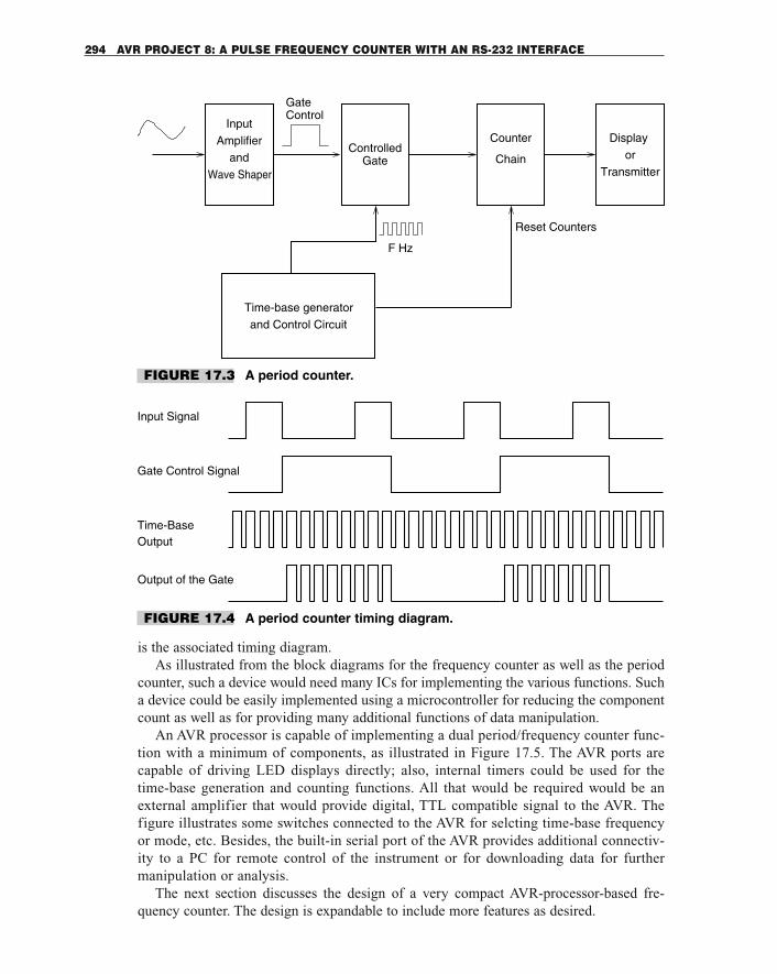
is the associated timing diagram.As illustrated from the block diagrams for the frequency counter as well as the period
counter, such a device would need many ICs for implementing the various functions. Sucha device could be easily implemented using a microcontroller for reducing the componentcount as well as for providing many additional functions of data manipulation.
An AVR processor is capable of implementing a dual period/frequency counter func-tion with a minimum of components, as illustrated in Figure 17.5. The AVR ports arecapable of driving LED displays directly; also, internal timers could be used for thetime-base generation and counting functions. All that would be required would be anexternal amplifier that would provide digital, TTL compatible signal to the AVR. Thefigure illustrates some switches connected to the AVR for selcting time-base frequencyor mode, etc. Besides, the built-in serial port of the AVR provides additional connectiv-ity to a PC for remote control of the instrument or for downloading data for furthermanipulation or analysis.
The next section discusses the design of a very compact AVR-processor-based fre-quency counter. The design is expandable to include more features as desired.
294 AVR PROJECT 8: A PULSE FREQUENCY COUNTER WITH AN RS-232 INTERFACE
GateControl
Time-base generator
and Control Circuit
ControlledGate
Input
Amplifier
Wave Shaper
and
Counter
Chain
Display
or
Transmitter
F Hz
Reset Counters
Input Signal
Gate Control Signal
Time-Base Output
Output of the Gate
FIGURE 17.3 A period counter.
FIGURE 17.4 A period counter timing diagram.
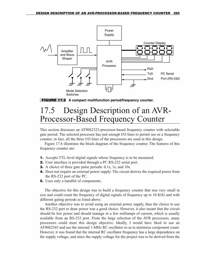
17.5 Design Description of an AVR-Processor-Based Frequency CounterThis section discusses an AT90S2323-processor-based frequency counter with selectablegate period. The selected processor has just enough I/O lines to permit use as a frequencycounter; in fact, all the three I/O lines of the processors are used in this design.
Figure 17.6 illustrates the block diagram of the frequency counter. The features of thisfrequency counter are:
1. Accepts TTL-level digital signals whose frequency is to be measured.2. User interface is provided through a PC RS-232 serial port.3. A choice of three gate pulse periods: 0.1s, 1s, and 10s.4. Does not require an external power supply. The circuit derives the required power from
the RS-232 port of the PC.5. Uses only a handful of components.
The objective for this design was to build a frequency counter that was very small insize and could count the frequency of digital signals of frequency up to 10 KHz and withdifferent gating periods as listed above.
Another objective was to avoid using an external power supply, thus the choice to usethe RS-232 port to draw power was a good choice. However, it also meant that the circuitshould be low power and should manage in a few milliamps of current, which is usuallyavailable from an RS-232 port. From the large selection of the AVR processors, manyprocessors could meet this design objective. Ideally, I would have liked to use anAT90S2343 and use the internal 1-MHz RC oscillator so as to minimize component count.However, it was found that the internal RC oscillator frequency has a large dependence onthe supply voltage, and since the supply voltage for the project was to be derived from the
DESIGN DESCRIPTION OF AN AVR-PROCESSOR-BASED FREQUENCY COUNTER 295
PowerSupply
Gnd
TxD
RxD
Port (RS-232)
PC Serial
Amplifierand Wave
ShaperAVR
Processor
Mode SelectionSwitches
Counter Display
FIGURE 17.5 A compact multifunction period/frequency counter.
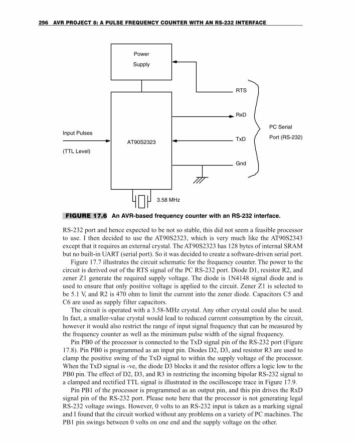
RS-232 port and hence expected to be not so stable, this did not seem a feasible processorto use. I then decided to use the AT90S2323, which is very much like the AT90S2343except that it requires an external crystal. The AT90S2323 has 128 bytes of internal SRAMbut no built-in UART (serial port). So it was decided to create a software-driven serial port.
Figure 17.7 illustrates the circuit schematic for the frequency counter. The power to thecircuit is derived out of the RTS signal of the PC RS-232 port. Diode D1, resistor R2, andzener Z1 generate the required supply voltage. The diode is 1N4148 signal diode and isused to ensure that only positive voltage is applied to the circuit. Zener Z1 is selected tobe 5.1 V, and R2 is 470 ohm to limit the current into the zener diode. Capacitors C5 andC6 are used as supply filter capacitors.
The circuit is operated with a 3.58-MHz crystal. Any other crystal could also be used.In fact, a smaller-value crystal would lead to reduced current consumption by the circuit,however it would also restrict the range of input signal frequency that can be measured bythe frequency counter as well as the minimum pulse width of the signal frequency.
Pin PB0 of the processor is connected to the TxD signal pin of the RS-232 port (Figure17.8). Pin PB0 is programmed as an input pin. Diodes D2, D3, and resistor R3 are used toclamp the positive swing of the TxD signal to within the supply voltage of the processor.When the TxD signal is -ve, the diode D3 blocks it and the resistor offers a logic low to thePB0 pin. The effect of D2, D3, and R3 in restricting the incoming bipolar RS-232 signal toa clamped and rectified TTL signal is illustrated in the oscilloscope trace in Figure 17.9.
Pin PB1 of the processor is programmed as an output pin, and this pin drives the RxDsignal pin of the RS-232 port. Please note here that the processor is not generating legalRS-232 voltage swings. However, 0 volts to an RS-232 input is taken as a marking signaland I found that the circuit worked without any problems on a variety of PC machines. ThePB1 pin swings between 0 volts on one end and the supply voltage on the other.
296 AVR PROJECT 8: A PULSE FREQUENCY COUNTER WITH AN RS-232 INTERFACE
RxD
TxD
Gnd
PC Serial
Port (RS-232)Input Pulses
(TTL Level)
AT90S2323
3.58 MHz
Power
Supply
RTS
FIGURE 17.6 An AVR-based frequency counter with an RS-232 interface.
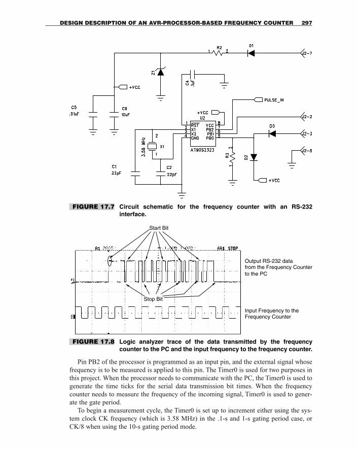
Pin PB2 of the processor is programmed as an input pin, and the external signal whosefrequency is to be measured is applied to this pin. The Timer0 is used for two purposes inthis project. When the processor needs to communicate with the PC, the Timer0 is used togenerate the time ticks for the serial data transmission bit times. When the frequencycounter needs to measure the frequency of the incoming signal, Timer0 is used to gener-ate the gate period.
To begin a measurement cycle, the Timer0 is set up to increment either using the sys-tem clock CK frequency (which is 3.58 MHz) in the .1-s and 1-s gating period case, orCK/8 when using the 10-s gating period mode.
DESIGN DESCRIPTION OF AN AVR-PROCESSOR-BASED FREQUENCY COUNTER 297
FIGURE 17.7 Circuit schematic for the frequency counter with an RS-232 interface.
Frequency CounterInput Frequency to the
Output RS-232 datafrom the Frequency Counterto the PC
Stop Bit
Start Bit
FIGURE 17.8 Logic analyzer trace of the data transmitted by the frequencycounter to the PC and the input frequency to the frequency counter.
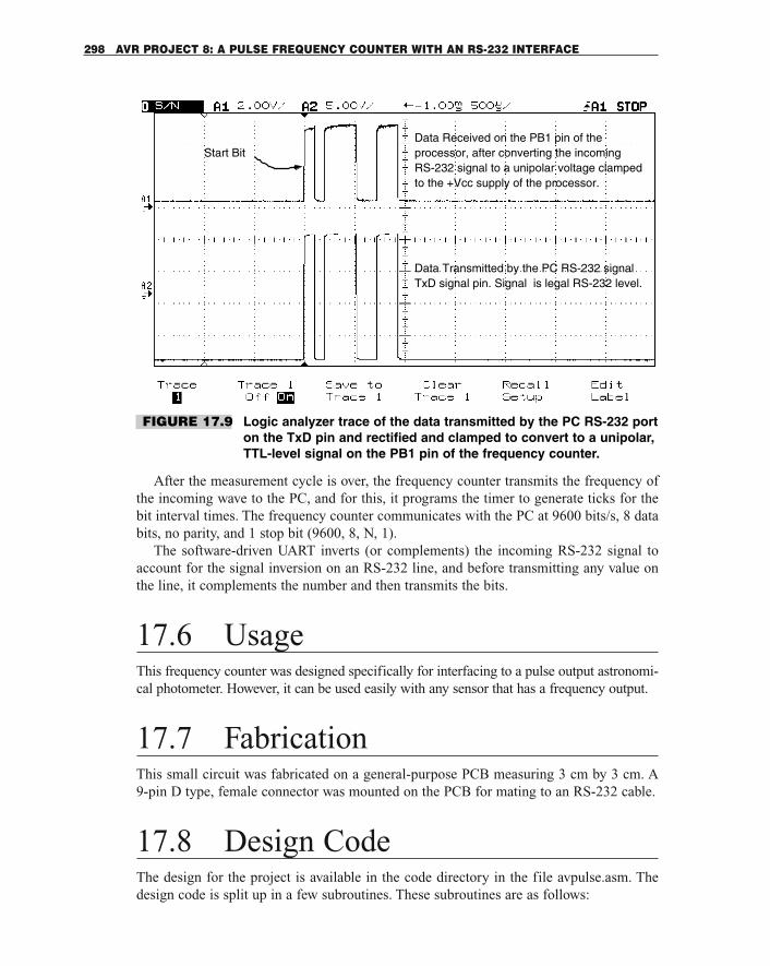
After the measurement cycle is over, the frequency counter transmits the frequency ofthe incoming wave to the PC, and for this, it programs the timer to generate ticks for thebit interval times. The frequency counter communicates with the PC at 9600 bits/s, 8 databits, no parity, and 1 stop bit (9600, 8, N, 1).
The software-driven UART inverts (or complements) the incoming RS-232 signal toaccount for the signal inversion on an RS-232 line, and before transmitting any value onthe line, it complements the number and then transmits the bits.
17.6 UsageThis frequency counter was designed specifically for interfacing to a pulse output astronomi-cal photometer. However, it can be used easily with any sensor that has a frequency output.
17.7 FabricationThis small circuit was fabricated on a general-purpose PCB measuring 3 cm by 3 cm. A 9-pin D type, female connector was mounted on the PCB for mating to an RS-232 cable.
17.8 Design CodeThe design for the project is available in the code directory in the file avpulse.asm. Thedesign code is split up in a few subroutines. These subroutines are as follows:
298 AVR PROJECT 8: A PULSE FREQUENCY COUNTER WITH AN RS-232 INTERFACE
Data Received on the PB1 pin of theprocessor, after converting the incomingRS-232 signal to a unipolar voltage clampedto the +Vcc supply of the processor.
Data Transmitted by the PC RS-232 signal TxD signal pin. Signal is legal RS-232 level.
Start Bit
FIGURE 17.9 Logic analyzer trace of the data transmitted by the PC RS-232 porton the TxD pin and rectified and clamped to convert to a unipolar,TTL-level signal on the PB1 pin of the frequency counter.
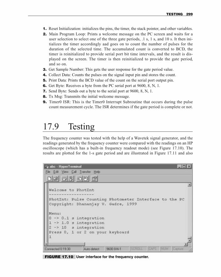
1. Reset Initialization: initializes the pins, the timer, the stack pointer, and other variables.2. Main Program Loop: Prints a welcome message on the PC screen and waits for a
user selection to select one of the three gate periods, .1 s, 1 s, and 10 s. It then ini-tializes the timer accordingly aad goes on to count the number of pulses for theduration of the selected time. The accumulated count is converted to BCD, thetimer is reinitialized to provide serial port bit time intervals, and the result is dis-played on the screen. The timer is then reinitialized to provide the gate period, and so on.
3. Get Sample Number: This gets the user response for the gate period value.4. Collect Data: Counts the pulses on the signal input pin and stores the count.5. Print Data: Prints the BCD value of the count on the serial port output pin.6. Get Byte: Receives a byte from the PC serial port at 9600, 8, N, 1.7. Send Byte: Sends out a byte to the serial port at 9600, 8, N, 1.8. Tx Msg: Transmits the initial welcome message.9. Timer0 ISR: This is the Timer0 Interrupt Subroutine that occurs during the pulse
count measurement cycle. The ISR determines if the gate period is complete or not.
17.9 TestingThe frequency counter was tested with the help of a Wavetek signal generator, and thereadings generated by the frequency counter were compared with the readings on an HPoscilloscope (which has a built-in frequency readout mode) (see Figure 17.10). Theresults are plotted for the 1-s gate period and are illustrated in Figure 17.11 and also
TESTING 299
FIGURE 17.10 User interface for the frequency counter.
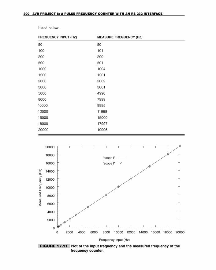
listed below.
FREQUENCY INPUT (HZ) MEASURE FREQUENCY (HZ)
50 50
100 101
200 200
500 501
1000 1004
1200 1201
2000 2002
3000 3001
5000 4998
8000 7999
10000 9995
12000 11998
15000 15000
18000 17997
20000 19996
300 AVR PROJECT 8: A PULSE FREQUENCY COUNTER WITH AN RS-232 INTERFACE
0
2000
4000
6000
8000
10000
12000
14000
16000
18000
20000
0 2000 4000 6000 8000 10000 12000 14000 16000 18000 20000
"scope1"
"scope1"
Frequency Input (Hz)
Mea
sure
d F
requ
ency
(H
z)
FIGURE 17.11 Plot of the input frequency and the measured frequency of thefrequency counter.
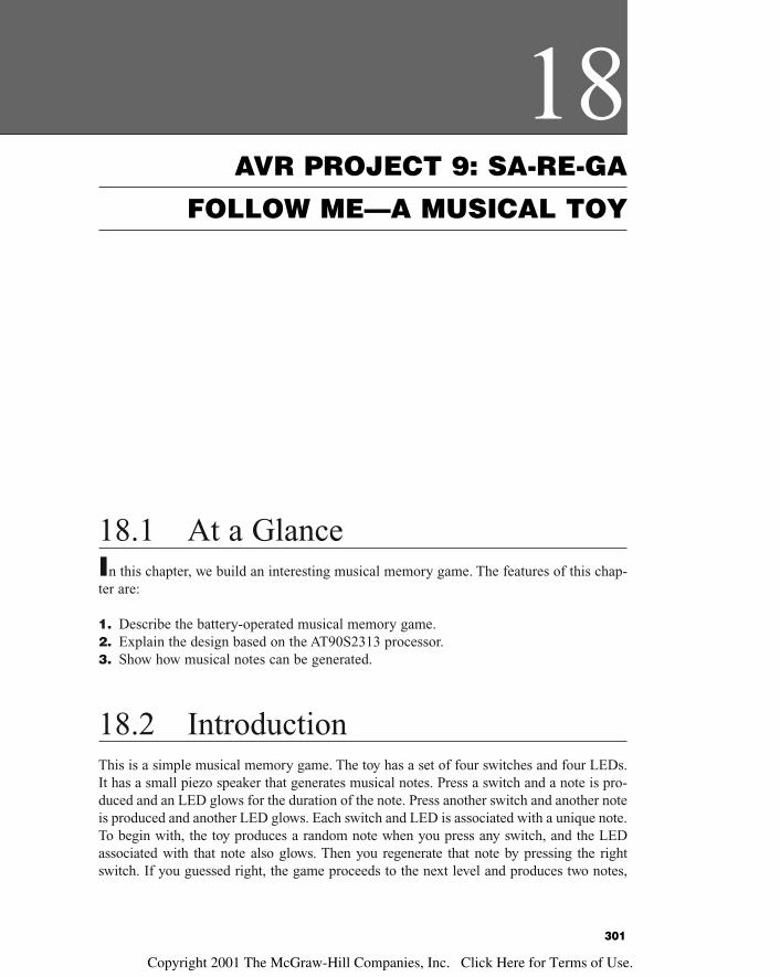
18.1 At a GlanceIn this chapter, we build an interesting musical memory game. The features of this chap-ter are:
1. Describe the battery-operated musical memory game.2. Explain the design based on the AT90S2313 processor.3. Show how musical notes can be generated.
18.2 IntroductionThis is a simple musical memory game. The toy has a set of four switches and four LEDs.It has a small piezo speaker that generates musical notes. Press a switch and a note is pro-duced and an LED glows for the duration of the note. Press another switch and another noteis produced and another LED glows. Each switch and LED is associated with a unique note.To begin with, the toy produces a random note when you press any switch, and the LEDassociated with that note also glows. Then you regenerate that note by pressing the rightswitch. If you guessed right, the game proceeds to the next level and produces two notes,
18AVR PROJECT 9: SA-RE-GA
FOLLOW ME—A MUSICAL TOY
301
Copyright 2001 The McGraw-Hill Companies, Inc. Click Here for Terms of Use.
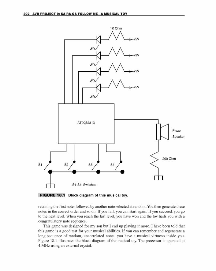
retaining the first note, followed by another note selected at random. You then generate thesenotes in the correct order and so on. If you fail, you can start again. If you succeed, you goto the next level. When you reach the last level, you have won and the toy hails you with acongratulatory note sequence.
This game was designed for my son but I end up playing it more. I have been told thatthis game is a good test for your musical abilities. If you can remember and regenerate along sequence of random, uncorrelated notes, you have a musical virtuoso inside you.Figure 18.1 illustrates the block diagram of the musical toy. The processor is operated at 4 MHz using an external crystal.
302 AVR PROJECT 9: SA-RA-GA FOLLOW ME—A MUSICAL TOY
Piezo
Speaker
200 Ohm
S1-S4: Switches
+5V
+5V
+5V
+5V
AT90S2313
1K Ohm
S4S3S2S1
FIGURE 18.1 Block diagram of this musical toy.
18.3 Design DescriptionLet us now consider the design of the toy. The processor chosen for this project isAT90S2313, considering the amount of I/O (total 9 I/O pins required) and the softwarecomplexity. An AT90S1200 was considered, and considering the software complexity, Idecided to use 2313 for this project, the reason being the need for SRAM for storing therandom notes that would be played during the course of the game. These notes need to bestored for later comparison with the user response. Since the AT90S1200 is not equippedwith any SRAM, it could not be employed.
The Timer0 is employed to generate the notes. The timer interrupt is used to occur attwice the rate of the required note frequency. The Timer ISR then toggles the output bit,which is connected to the piezo buzzer, generating a note at the required frequency (seeFigure 18.1).
The selected notes were of the frequencies 440 Hz, 494 Hz, 523 Hz, and 587 Hz. Timerreload values corresponding to these notes were calculated for a clock frequency of 4 MHz.
At reset and each time the user loses and starts to play again, the program creates a tableof 32 entries with random numbers using the Linear Feedback Shift Register (LFSR) prin-ciple. The Timer0, which is free-running, is used once at this time to get a seed number forthe LFSR algorithm. After this the Timer0 is used only for generating audio notes. The pro-gram then waits for a key, any key, to be pressed and plays the first note using the randomnumber table entry. The LED corresponding to this note is also lit up. It then waits for theuser to press a key. If the key matches the note, the note is played again, the LED is lit upagain, and the program proceeds to the next level. Now it generates the first note again andanother note using the second entry from the random number table. Again, after playingthe notes, the program waits for the keys to be pressed in the right sequence. If the keysmatch the note played, the program proceeds to the next level. This can go on until all the32 notes have been played. If the user has been able to play back the correct sequence forall the 32 notes, the user wins the game. Else, the program starts again, creating a new ran-dom number table. Before calling the random number generator, the interrupts are dis-abled. The routine to generate the random numbers is a critical section of the code thatneeds to run without being interrupted. After returning from the random number routine,the interrupts are enabled again.
Figure 18.2 illustrates the circuit schematic for the toy. The switches are connected tothe PORTD pins and the LEDs and the speaker to the PORTB pins. This arrangement wasdictated by Atmel’s AVR evaluation board on which the prototype was tested. The switch-es do not have any pull-up resistors as the internal pull resistors in the PORT pins are acti-vated. The LEDs are connected to sink current into the processor pin.
18.4 FabricationThis toy was initially developed on the Atmel’s AVR evaluation board. After that, it wasbuilt on a general-purpose PCB. It runs off a 9-V battery and a 78L05 regulator. Instead ofa 9-V battery, even four 1.5-V cells could be used.
DESIGN CODE 303
FIGURE 18.2 Circuit schematic for the toy.
30
4
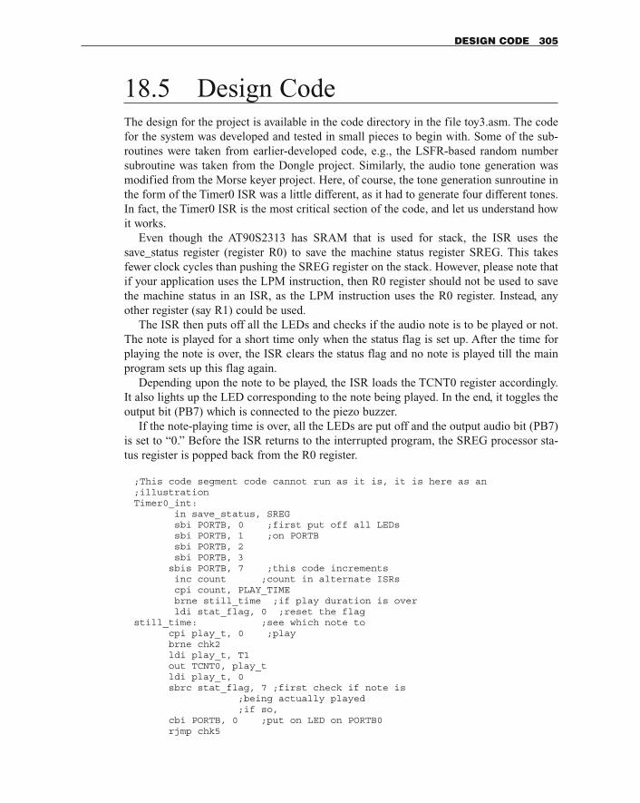
18.5 Design CodeThe design for the project is available in the code directory in the file toy3.asm. The codefor the system was developed and tested in small pieces to begin with. Some of the sub-routines were taken from earlier-developed code, e.g., the LSFR-based random numbersubroutine was taken from the Dongle project. Similarly, the audio tone generation wasmodified from the Morse keyer project. Here, of course, the tone generation sunroutine inthe form of the Timer0 ISR was a little different, as it had to generate four different tones.In fact, the Timer0 ISR is the most critical section of the code, and let us understand howit works.
Even though the AT90S2313 has SRAM that is used for stack, the ISR uses thesave_status register (register R0) to save the machine status register SREG. This takesfewer clock cycles than pushing the SREG register on the stack. However, please note thatif your application uses the LPM instruction, then R0 register should not be used to savethe machine status in an ISR, as the LPM instruction uses the R0 register. Instead, anyother register (say R1) could be used.
The ISR then puts off all the LEDs and checks if the audio note is to be played or not.The note is played for a short time only when the status flag is set up. After the time forplaying the note is over, the ISR clears the status flag and no note is played till the mainprogram sets up this flag again.
Depending upon the note to be played, the ISR loads the TCNT0 register accordingly.It also lights up the LED corresponding to the note being played. In the end, it toggles theoutput bit (PB7) which is connected to the piezo buzzer.
If the note-playing time is over, all the LEDs are put off and the output audio bit (PB7)is set to “0.” Before the ISR returns to the interrupted program, the SREG processor sta-tus register is popped back from the R0 register.
;This code segment code cannot run as it is, it is here as an;illustrationTimer0_int:
in save_status, SREGsbi PORTB, 0 ;first put off all LEDssbi PORTB, 1 ;on PORTBsbi PORTB, 2sbi PORTB, 3sbis PORTB, 7 ;this code incrementsinc count ;count in alternate ISRscpi count, PLAY_TIMEbrne still_time ;if play duration is overldi stat_flag, 0 ;reset the flag
still_time: ;see which note tocpi play_t, 0 ;playbrne chk2ldi play_t, T1out TCNT0, play_tldi play_t, 0sbrc stat_flag, 7 ;first check if note is
;being actually played;if so,
cbi PORTB, 0 ;put on LED on PORTB0rjmp chk5
DESIGN CODE 305
chk2: cpi play_t, 1brne chk3ldi play_t, T2out TCNT0, play_tldi play_t, 1sbrc stat_flag, 7cbi PORTB, 1 ;put on LED on PORTB1rjmp chk5
chk3: cpi play_t, 2brne chk4ldi play_t, T3out TCNT0, play_tldi play_t, 2sbrc stat_flag, 7cbi PORTB, 2 ;put on LED on PORTB2rjmp chk5
chk4: ldi play_t, T4out TCNT0, play_tldi play_t, 3sbrc stat_flag, 7cbi PORTB, 3 ;put on LED on PORTB3
;check if flag to play note;is set to 255
chk5: cpi stat_flag, 255breq play_itcbi PORTB, 7 ;if no, then clear PB7, so
;that the speaker does not load;PB7
rjmp no_tone ;note is not to be played;so just return back;if flag is set, then play note;for that just complement PB7;stat_flag is being used as a temp;register. Its value is restored;later.
play_it: in stat_flag, PORTBldi temp2, $80eor stat_flag, temp2out PORTB, stat_flagldi stat_flag, 255
no_tone: out SREG, save_statusreti
Figure 18.3 illustrates one of the notes being played by the toy. Now that the toy is work-ing well, my son and I are having a great time playing with it.
306 AVR PROJECT 9: SA-RA-GA FOLLOW ME—A MUSICAL TOY
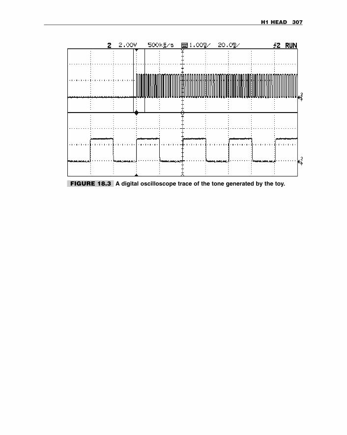
H1 HEAD 307
FIGURE 18.3 A digital oscilloscope trace of the tone generated by the toy.

This page intentionally left blank.
19.1 At a Glance
1. A simple and inexpensive application prototyping board.2. Uses the STK200 dongle for program download.3. Uses Atmel AVR ISP software for project management.4. Offers a general-purpose prototyping area to add custom hardware.5. Allows all classic 20-pin AVR controllers to be used.6. Can be modified to suit other AVR processors.
19.2 IntroductionThis chapter looks at a simple and inexpensive prototyping board for developing AVRapplications.
However, I want to make it clear that some really inexpensive and compact prototypingand evaluation boards are available through Atmel. These boards have more features and
19AVR PROJECT 10:
AVR PROTOBOARD™ FOR NUTS™
309
Copyright 2001 The McGraw-Hill Companies, Inc. Click Here for Terms of Use.
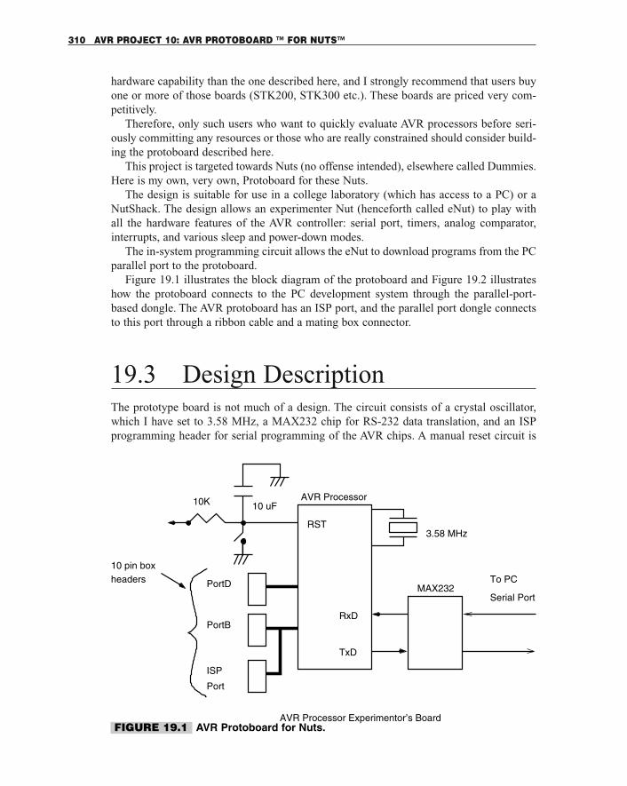
hardware capability than the one described here, and I strongly recommend that users buyone or more of those boards (STK200, STK300 etc.). These boards are priced very com-petitively.
Therefore, only such users who want to quickly evaluate AVR processors before seri-ously committing any resources or those who are really constrained should consider build-ing the protoboard described here.
This project is targeted towards Nuts (no offense intended), elsewhere called Dummies.Here is my own, very own, Protoboard for these Nuts.
The design is suitable for use in a college laboratory (which has access to a PC) or aNutShack. The design allows an experimenter Nut (henceforth called eNut) to play withall the hardware features of the AVR controller: serial port, timers, analog comparator,interrupts, and various sleep and power-down modes.
The in-system programming circuit allows the eNut to download programs from the PCparallel port to the protoboard.
Figure 19.1 illustrates the block diagram of the protoboard and Figure 19.2 illustrateshow the protoboard connects to the PC development system through the parallel-port-based dongle. The AVR protoboard has an ISP port, and the parallel port dongle connectsto this port through a ribbon cable and a mating box connector.
19.3 Design DescriptionThe prototype board is not much of a design. The circuit consists of a crystal oscillator,which I have set to 3.58 MHz, a MAX232 chip for RS-232 data translation, and an ISPprogramming header for serial programming of the AVR chips. A manual reset circuit is
310 AVR PROJECT 10: AVR PROTOBOARD ™ FOR NUTS™
10K
RST
TxD
RxD
3.58 MHz
AVR Processor10 uF
AVR Processor Experimentor’s Board
ISP
Port
PortB
PortD
10 pin boxheaders
MAX232To PC
Serial Port
FIGURE 19.1 AVR Protoboard for Nuts.
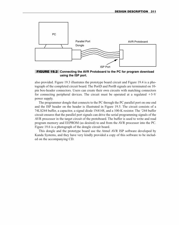
also provided. Figure 19.3 illustrates the prototype board circuit and Figure 19.4 is a pho-tograph of the completed circuit board. The PortD and PortB signals are terminated on 10-pin box-header connectors. Users can create their own circuits with matching connectorsfor connecting peripheral devices. The circuit must be operated at a regulated �5-V power supply.
The programmer dongle that connects to the PC through the PC parallel port on one endand the ISP header on the header is illustrated in Figure 19.5. The circuit consists of a74LS244 buffer, a capacitor, a signal diode 1N4148, and a 100-K resistor. The ‘244 buffercircuit ensures that the parallel port signals can drive the serial programming signals of theAVR processor in the target circuit of the protoboard. The buffer is used to write and readprogram memory and EEPROM (as desired) to and from the AVR processor into the PC.Figure 19.6 is a photograph of the dongle circuit board.
This dongle and the prototype board use the Atmel AVR ISP software developed byKanda Systems, and they have very kindly provided a copy of this software to be includ-ed on the accompanying CD.
DESIGN DESCRIPTION 311
AVR Protoboard
ISP Port
Parallel Port
Dongle
PC
FIGURE 19.2 Connecting the AVR Protoboard to the PC for program downloadusing the ISP port.
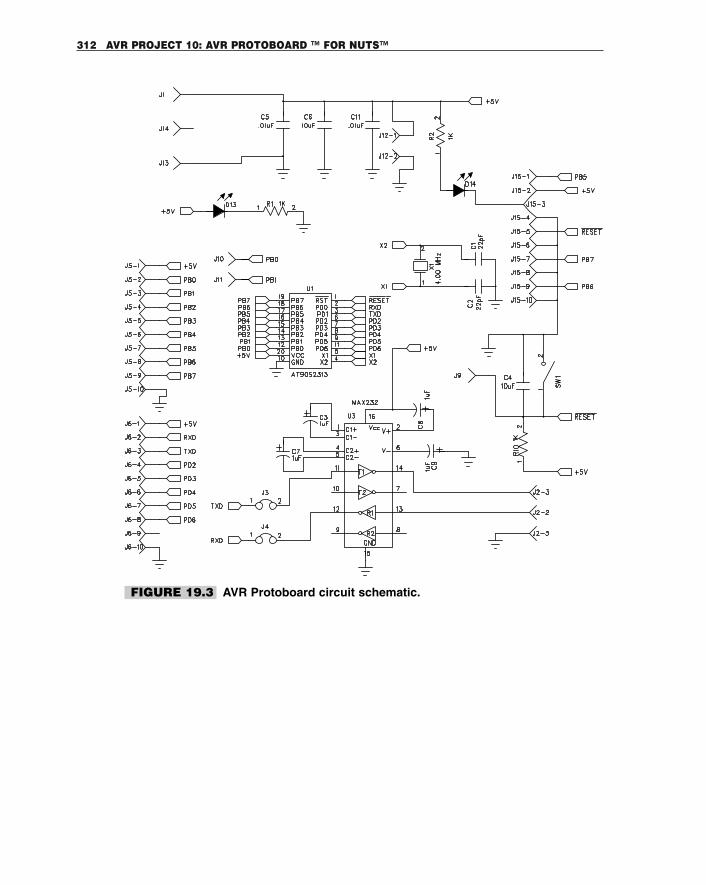
312 AVR PROJECT 10: AVR PROTOBOARD ™ FOR NUTS™
FIGURE 19.3 AVR Protoboard circuit schematic.
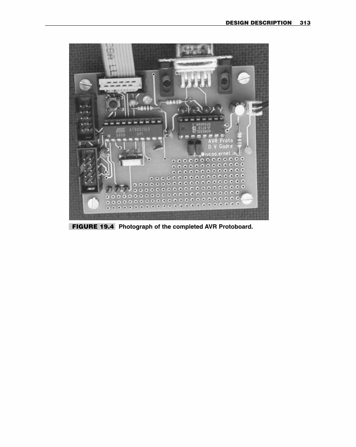
DESIGN DESCRIPTION 313
FIGURE 19.4 Photograph of the completed AVR Protoboard.
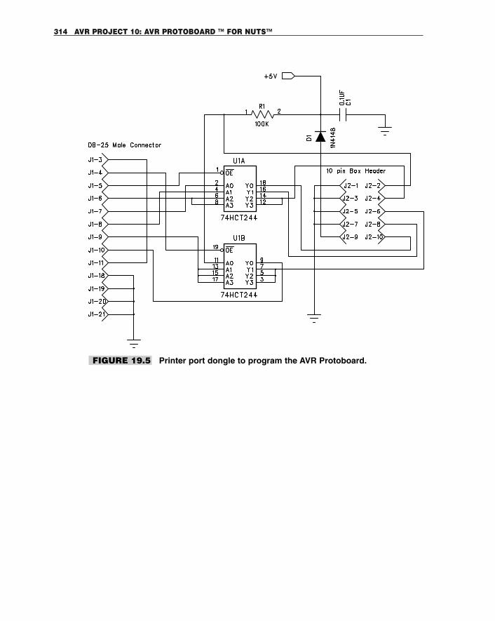
314 AVR PROJECT 10: AVR PROTOBOARD ™ FOR NUTS™
FIGURE 19.5 Printer port dongle to program the AVR Protoboard.
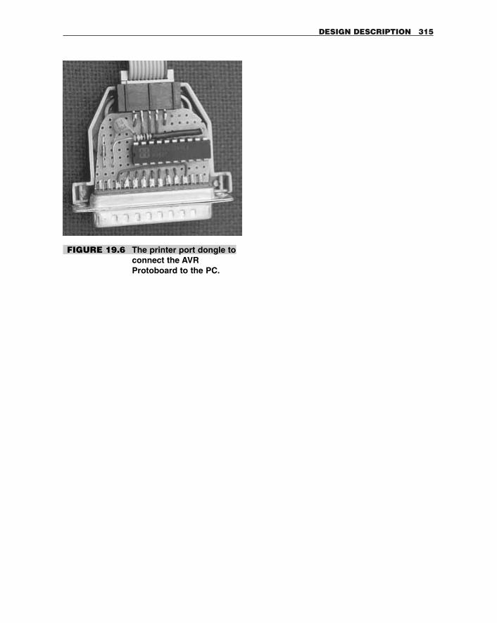
DESIGN DESCRIPTION 315
FIGURE 19.6 The printer port dongle toconnect the AVRProtoboard to the PC.

This page intentionally left blank.
20.1 AT90S2343 Controller-basedCode AuthenticatorThe idea of this circuit is to provide a very simple code authentication scheme. The circuitis based on the AT90S2343 AVR controller. It has three input keys and two output LEDsfor visual feedback. These LED outputs are also used to provide a “Valid” signal when theentered key sequence is correct.
The input keys are labeled “0,” “1,” and “New.” To enter a key sequence, the “New” keyis pressed followed by the sequence of keys for the code, “0” or “1.” After each key press,the “Ack” LED indicates that the key press is recognized. For an error, the “Ack” and the“OK” LEDs blink alternately. If the entered key sequence is correct, both of these LEDsgo ON at the same time and stay on for five seconds (Figure 20.1).
20IDEAS FOR PROJECTS
317
Copyright 2001 The McGraw-Hill Companies, Inc. Click Here for Terms of Use.
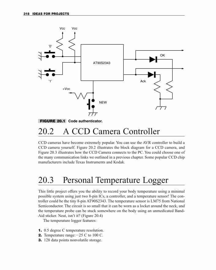
20.2 A CCD Camera ControllerCCD cameras have become extremely popular. You can use the AVR controller to build aCCD camera yourself. Figure 20.2 illustrates the block diagram for a CCD camera, andFigure 20.3 illustrates how the CCD Camera connects to the PC. You could choose one ofthe many communication links we outlined in a previous chapter. Some popular CCD chipmanufacturers include Texas Instruments and Kodak.
20.3 Personal Temperature LoggerThis little project offers you the ability to record your body temperature using a minimalpossible system using just two 8-pin ICs, a controller, and a temperature sensor! The con-troller could be the tiny 8-pin AT90S2343. The temperature sensor is LM75 from NationalSemiconductor. The circuit is so small that it can be worn as a locket around the neck, andthe temperature probe can be stuck somewhere on the body using an unmedicated Band-Aid sticker. Neat, isn’t it? (Figure 20.4)
The temperature logger features:
1. 0.5 degree C temperature resolution.2. Temperature range:�25 C to 100 C.3. 128 data points nonvolatile storage.
318 IDEAS FOR PROJECTS
NEW
’1’
’0’
Ack
OK
Vcc Vcc
+Vcc
AT90S2343
FIGURE 20.1 Code authenticator.
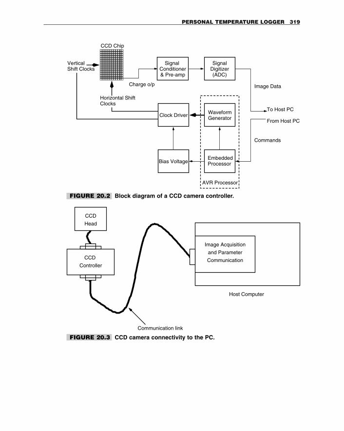
PERSONAL TEMPERATURE LOGGER 319
VerticalShift Clocks
Horizontal ShiftClocks
Charge o/p
Signal Conditioner& Pre-amp
Clock Driver
Bias Voltage
WaveformGenerator
EmbeddedProcessor
SignalDigitizer(ADC)
To Host PC
Image Data
From Host PC
Commands
CCD Chip
AVR Processor
FIGURE 20.2 Block diagram of a CCD camera controller.
Image Acquisition
and Parameter
Communication
Host Computer
CCD
Controller
CCD
Head
Communication link
FIGURE 20.3 CCD camera connectivity to the PC.
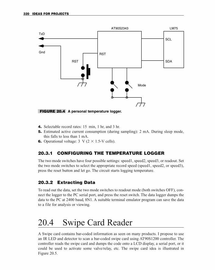
4. Selectable record rates: 15 min, 1 hr, and 3 hr.5. Estimated active current consumption (during sampling): 2 mA. During sleep mode,
this falls to less than 1 mA.6. Operational voltage: 3 V (2 � 1.5-V cells).
20.3.1 CONFIGURING THE TEMPERATURE LOGGER
The two mode switches have four possible settings: speed1, speed2, speed3, or readout. Setthe two mode switches to select the appropriate record speed (speed1, speed2, or speed3),press the reset button and let go. The circuit starts logging temperature.
20.3.2 Extracting Data
To read out the data, set the two mode switches to readout mode (both switches OFF), con-nect the logger to the PC serial port, and press the reset switch. The data logger dumps thedata to the PC at 2400 baud, 8N1. A suitable terminal emulator program can save the datato a file for analysis or viewing.
20.4 Swipe Card ReaderA Swipe card contains bar-coded information as seen on many products. I propose to usean IR LED and detector to scan a bar-coded swipe card using AT90S1200 controller. Thecontroller reads the swipe card and dumps the code onto a LCD display, a serial port, or itcould be used to activate some valve/relay, etc. The swipe card idea is illustrated in Figure 20.5.
320 IDEAS FOR PROJECTS
LM75
Mode
RST
SCL
SDA
AT90S2343
Gnd
RST
TxD
FIGURE 20.4 A personal temperature logger.
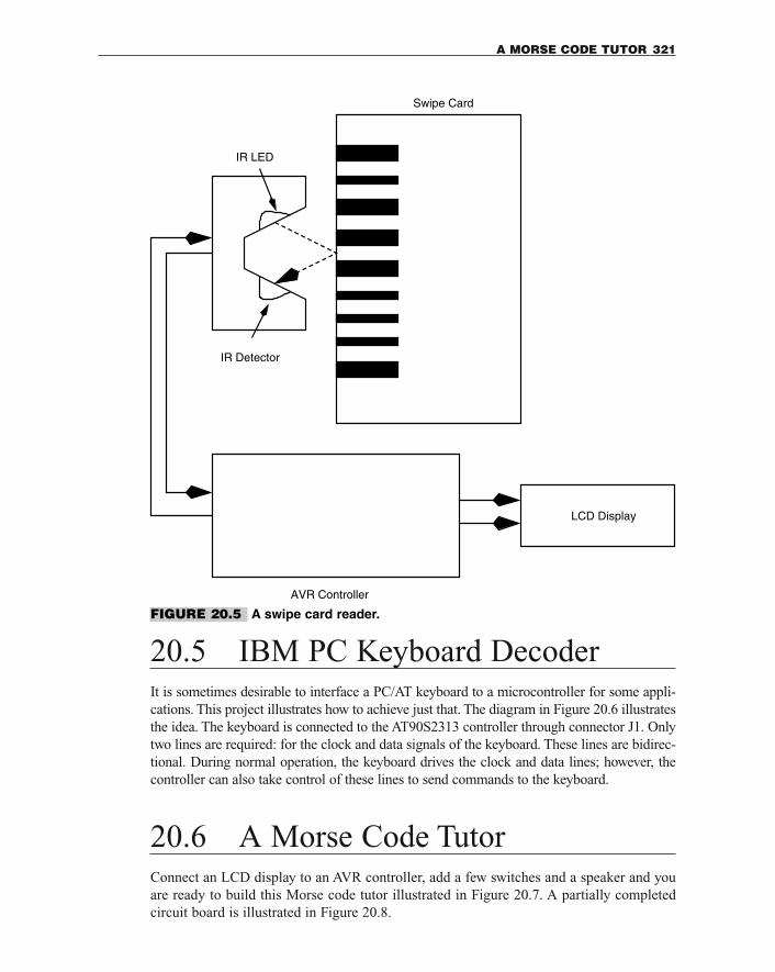
20.5 IBM PC Keyboard DecoderIt is sometimes desirable to interface a PC/AT keyboard to a microcontroller for some appli-cations. This project illustrates how to achieve just that. The diagram in Figure 20.6 illustratesthe idea. The keyboard is connected to the AT90S2313 controller through connector J1. Onlytwo lines are required: for the clock and data signals of the keyboard. These lines are bidirec-tional. During normal operation, the keyboard drives the clock and data lines; however, thecontroller can also take control of these lines to send commands to the keyboard.
20.6 A Morse Code TutorConnect an LCD display to an AVR controller, add a few switches and a speaker and youare ready to build this Morse code tutor illustrated in Figure 20.7. A partially completedcircuit board is illustrated in Figure 20.8.
A MORSE CODE TUTOR 321
Swipe Card
IR LED
IR Detector
AVR Controller
LCD Display
FIGURE 20.5 A swipe card reader.
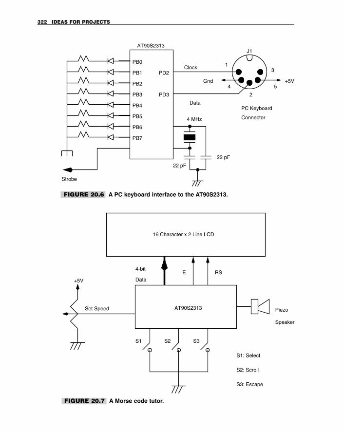
322 IDEAS FOR PROJECTS
Strobe
AT90S2313
Clock
DataPC Keyboard
Connector
Gnd +5V
J1
1
2
3
4 5
PB0
PB1
PB2
PB3
PB4
PB5
PB6
PB7
PD2
PD3
4 MHz
22 pF
22 pF
FIGURE 20.6 A PC keyboard interface to the AT90S2313.
16 Character x 2 Line LCD
4-bit
DataE RS
AT90S2313 Piezo
Speaker
S2 S3S1
S1: Select
S2: Scroll
S3: Escape
+5V
Set Speed
FIGURE 20.7 A Morse code tutor.
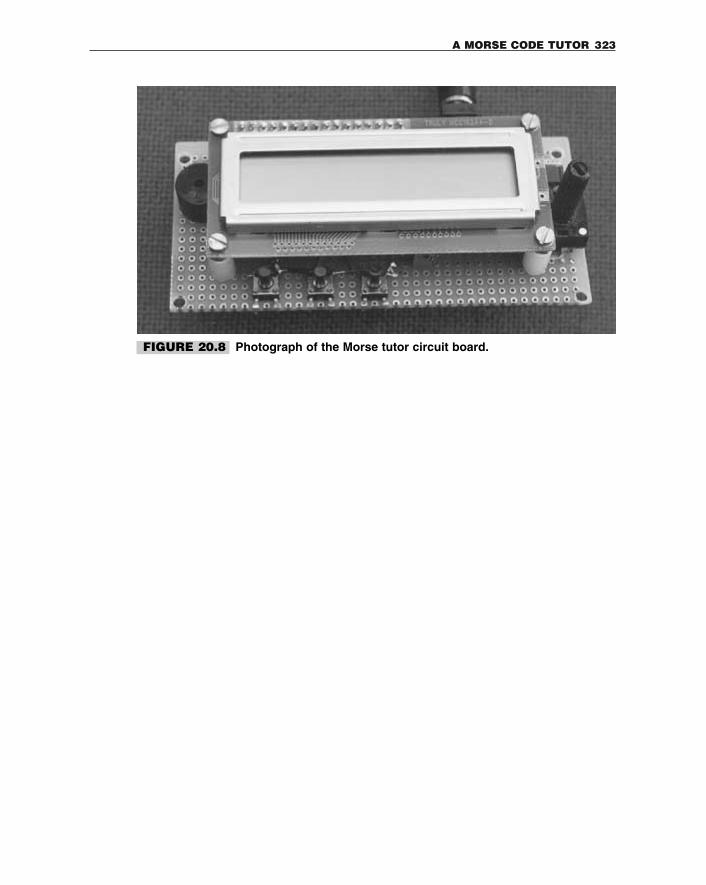
A MORSE CODE TUTOR 323
FIGURE 20.8 Photograph of the Morse tutor circuit board.

This page intentionally left blank.
ADC: Acronym for Analog to Digital Converter. An electronic device or system thatencodes analog voltage/current to a multilevel digital number.
address bus: A group of signals in a microprocessor system that indicates the addressof the memory location from where the data is to be read or written to.
ASCII: American Standards Committee for Information Interchange. A 7-bit codingscheme for alphabets, numerals, punctuation, as well as control characters.
ASIC: Acronym for Application Specific Integrated Circuit.assembler: A software program that takes a text file called the source file, and converts
it into another file with the machine op-codes (simply called the machine code or objectcode).
BCD: Acronym for Binary Coded Decimal.BOD: Brownout Detector. An electronic device that detects a drop in supply voltage
below a threshold and generates a signal to reset the processor till the supply voltage isrestored to acceptable level.
BIT: Binary digit.bps: Acronym for Bits per Second.byte: A number with a maximum of eight bits. Thus the byte-wide number is between 0
and 255 (decimal).CISC: Acronym for Complex Instruction Set Computer. This a type of processor archi-
tecture that is characterized by a variable instruction length, usually small numbers ofregister and multiple address modes.
GLOSSARY
325
Copyright 2001 The McGraw-Hill Companies, Inc. Click Here for Terms of Use.
compiler: A software program that converts a high-level language source code into themachine language that the processor can execute.
counter: A register that is incremented for each occurrence of an event on an input pinof the counter. The event is indicated by a pulse. For each pulse, the counter is incre-mented by one.
critical section: A chunk of code that must be executed without any interruption forproper operation.
CPLD: Acronym for Complex Programmable Logic Device. A programmable logicdevice rich in gates and interconnection circuitry.
CPU: Acronym for Central Processing Unit. The CPU is the computational and controlunit of a computer.
DAC: Acronym for Digital to Analog Converter. A device or a process that converts adigital number to a corresponding analog voltage or current.
data bus: A set of signals that carries the data information between the processor andthe memory and/or I/O devices.
debug: To correct mistakes in a program.debugger: A software program that assists in debugging a piece of code.development host: A computer system that hosts development software like an assem-
bler, compiler, programmer, debugger, etc.dongle: A mechanism to ensure that only authorized users can use a particular software
with the help of an electronic lock provided with the software to deter software piracy.The dongle needs to be connected to the PC parallel port, serial port, or the USB to beable to use the software.
duplex: Term used in communication systems that means that both the transmitter andthe receiver can send and receive signals at the same time.
embedded controller: A piece of hardware including some processor and software thatcontrols a device.
emulator: A device that mimics the behavior and functions of another device. A proces-sor emulator.
EMI: Acronym for Electro-Magnetic Interference. This is a phenomenon by which adevice or a system can generate an electromagnetic field in the radio frequency spectrumwith the potential to disrupt operation of other electronic components or systems in thevicinity.
EEPROM: Acronym for Electrically Erasable and Programmable Read Only Memory.EPROM: Acronym for Electrically Programmable Read Only Memory.finite state machine: A device that stores the status of something at a given time, with
some inputs that can change the state and/or outputs.flag: A bit used by a program to remember something or to convey binary information
to another piece of program.flash memory: A nonvolatile memory that can be erased and reprogrammed in units of
memory called blocks. The name flash memory means the memory cells can be erasedin an electron tunneling process in a flash by removing an electronic charge from a float-ing gate associated with each memory cell.
FPGA: Acronym for Field Programmable Gate Array. A large and dense programmablelogic device.
FSM: Acronym for Finite State Machine.
326 GLOSSARY
full-duplex: Same as Duplex.glitch: An unwanted, transient signal transition from the current level to the other level
and back to the original level.half-duplex: Term used in communication systems that means that either the transmit-
ter can send or the receiver can receive signals at a given time.handshake signal: Control and feedback signals used between two (or more) devices to
facilitate exchange of data.hexadecimal: A base-16 number system. The numbers go from 0 to 9, A, B, C, D, E,
and F.host: A computer system acting as a master that provides services to other connected
devices or systems.IC: Acronym for Integrated Circuit. A semiconductor chip with many transistors and
resistors connected to make an electronic circuit.ICE: Acronym for In-Circuit Emulator. A development tool for developing micro-
processor-based system and devices. The ICE mimics the operation of the target proces-sor during the development process.
IIC or I2C: Acronym for Inter-IC communication. A communication bus with only twosignals.
infrared: Part of the light spectrum that is just above that of visible light in the red endof the spectrum.
IrDA: Acronym for Infrared Data Association. IrDA is an industry-sponsored organiza-tion to design standards for the hardware and software used in infrared communicationlinks.
instruction: Lowest level command given to the processor by a program.interrupt: An asynchronous signal generated by a peripheral device to the processor
that, when asserted, indicates to the processor to take notice and execute a special pieceof program called an ISR.
I/O: Input Output. Peripheral devices of a processor to interact with the physical envi-ronment around it.
I/O map: A table containing the addresses, within the I/O space, of the input and outputdevices of a computer system.
I/O space: A type of addressing region that allows a processor to connect I/O devices.instruction pointer: A special register in a processor that points to an address in the pro-
gram memory from where the current instruction is being executed by the processor.ISA: Acronym for Industry Standard Architecture. ISA is a bus architecture used in IBM
personal computers. It allows connectivity between the processor and the associatedperipheral circuits and devices.
ISR: Acronym for Interrupt SubRoutine. A program that is executed by the processorwhen an interrupt occurs in a computer system.
interrupt vector: Address of an ISR.Kbps: Acronym for Kilobits per second. Kilo is 1000 here.Kbyte: Kilobyte. Kilo is 1024 here.latency: Usually associated with the interrupts in a computer system and refers to the
time it takes to respond to an interrupt signal.LED: Acronym for Light Emitting Diode. A semiconductor device that emits light when
a voltage of appropriate polarity and value is applied to it.
GLOSSARY 327
load-store architecture: A processor architecture in which the memory is accessedusing only the load and store commands. No other operations are allowed on the memo-ry contents directly.
logic analyzer: An instrument to observe digital signals as a function of time. The logicanalyzer has a fluorescent or LCD display that displays the digital signals.
logic gate: A digital circuit that has one or more inputs and an output. It performs a log-ical operation (such as AND, OR, XOR, XNOR, NAND, NOR, NOT) on the inputs andproduces a result on the output.
microcomputer: A Microprocessor and associated support circuitry, peripheral I/Ocomponents, and memory (program as well as data) put together to form a small com-puter specifically for data acquisition and control applications.
microcontroller: A microcomputer on a single chip.microprocessor: A Central Processor Unit (CPU) on a single chip.mnemonic: An abbreviation, an aid for remembering the code of a processor.NVRAM: Acronym for Non-Volatile Random Access Memory. RAM with battery
backup for retaining the contents of the RAM when the main power is put off.oscilloscope: An instrument to observe electrical signals as a function of time. It has a
fluorescent or LCD display for observing the signals.object code: A program that a processor can execute directly.pipeline: Refers to an internal implementation of a processor in which the instructions
are continuously being fetched by a section of the processor and placed in a queue forexecution by the execution section of the processor, which in turn places the results in anoutput queue to be stored back to the designated destination. A nonpipelined processor,on the other hand, fetches an instruction, executes it, and stores the results before fetch-ing the next instruction. Pipelining improves overall execution speed because of overlap-ping of the various stages of program execution.
PLD: Acronym for Programmable Logic Device. A digital circuit whose functionalitycan be changed as per the logic required. The PLD has a combination of AND, OR, andNOT gates connected through a network. By choosing the right gates and the right inter-connects, the PLD can be made to implement any logic function.
program counter: Same as Instruction Pointer.PWM: Acronym for Pulse Width Modulation. In PWM, the pulse width of the frequen-
cy is changed while keeping the frequency constant. This changes the DC value of thesignal. For low width pulse, the DC value is smaller than a pulse of higher width.
RAM: Acronym for Random Access Memory. A memory device any part of which canbe accessed directly. In the early days of computing, this was contrasted with tape mem-ory, which was sequential access memory. Now RAM usually means some sort ofvolatile, read/write memory.
RISC: Acronym for Reduced Instruction Set Computer. A type of computer architecturewith a small number of minimum instructions, characterized by a very regular instruc-tion structure of fixed length, a load-store approach to memory access, and a large num-ber of registers. Contrast it with CISC.
reset: To restart. A signal in a processor that initializes the internal register and controlcircuit to a default value and starts executing the program from the first memory loca-tion.
reset vector: Address of the reset code.
328 GLOSSARY
reset address: The address that the processor first accesses for the first instruction, afterthe reset signal is applied.
reset pointer: Address of the reset code.reset code: The program that the user writes as part of the system initialization.RMS: Acronym for Root Mean Square. A way to express the value of the signal by aver-
aging the square of the signal over a full cycle of the signal and then taking the root ofthe average quantity. The “220-V” or “115-V” wall outlet voltage in most countries is anRMS value. For a sine wave, the peak signal is about 1.4 times the RMS value of the sig-nal.
RS-232: A protocol for serial asynchronous transfer of data.simplex: Used in communication. Simplex refers to communication in only one direc-
tion and not in the reverse direction.simulator: A software for monitoring the execution of a program. Simulator allows the
user to execute the program instruction by instruction and inspect register, memory, andI/O port contents. The simulator allows sections of program to run at full speed by plac-ing break points.
SPI: Acronym for Serial Peripheral Interconnect. A four-wire serial synchronous serialcommunication protocol between two devices or ICs.
stack: A read/write storage space used for storing the return address of a calling pro-gram. The stack has a Last In First Out structure. The value written last is read first.
stack pointer: An address register that points to the current top location in the stack.startup code: A section of a program that is executed for system initialization at the very
beginning.timer: A counter that is incremented by a clock signal.target device: Refers to the processor in the target system that is under development.UART: Acronym for Universal Asynchronous Receiver Transmitter. A serial communi-
cation device or IC that converts a byte of data into serial bits and transmits it out at acertain rate. Similarly, it receives incoming serial bits and assembles these bits into a bytefor the host.
watchdog timer: A special timer that is used specifically for the purpose of resetting thesystem if it overflows. A piece of program resets the watchdog timer every so oftenbefore the watchdog timer expires. However, if the program fails to reset the timer, indi-cating that the program has crashed or entered into some infinite loop (indicatingunwanted and unexpected program or system behavior), the watchdog timer overflowsand this generates a processor reset signal.
GLOSSARY 329

This page intentionally left blank.
The following Web sites provide useful information about AVR controllers, soft-ware projects, etc.
Atmel AVR Page: http://www.atmel.com/atmel/products/prod23.htm
Atmel AVR Data Sheets: http://www.atmel.com/atmel/products/prod200.htm
Atmel AVR Application Notes:http://www.atmel.com/atmel/products/prod201.htm
Atmel AVR Support Tools:http://www.atmel.com/atmel/products/prod202.htm
Atmel AVR Software: http://www.atmel.com/atmel/products/prod203.htm
Atmel AVR Reference Library:http://www.atmel.com/atmel/products/prod204.htm
Atmel AVR Third Party Vendors:http://www.atmel.com/atmel/products/prod205.htm
AVR Resource and Information Center http://www.avr-forum.com/
Omega Verksted’s AVR Resource Page for projects and linkshttp://www.omegav.ntnu.no/avr/
APPENDIX
INTERNET RESOURCES FOR
THE AVR
331
Copyright 2001 The McGraw-Hill Companies, Inc. Click Here for Terms of Use.
Dontronics. AVR Kits, parts, projects, links, and much more. A very useful site.http://www.dontronics.com
Jack’s AVR Page. Projects, code, free JAVR Basic Compiler, kits.http://www3.igalaxy.net/ jackt/ or http://www.javrbasics.com
SPJ Systems. C compiler http://www.spjsystems.com
AVR Embedded Microcontroller Resources. Links, links, and links.http://www.ipass.net/hammill/newavr.htm
More AVR links and projects. http://come.to/Stelios_Cellar
AVR in education. A microcontroller design lab using the AVR. http://instruct1.cit.cor-nell.edu/courses/ee476/
332 APPENDIX

INDEX
Copyright 2001 The McGraw-Hill Companies, Inc. Click Here for Terms of Use.

This page intentionally left blank.
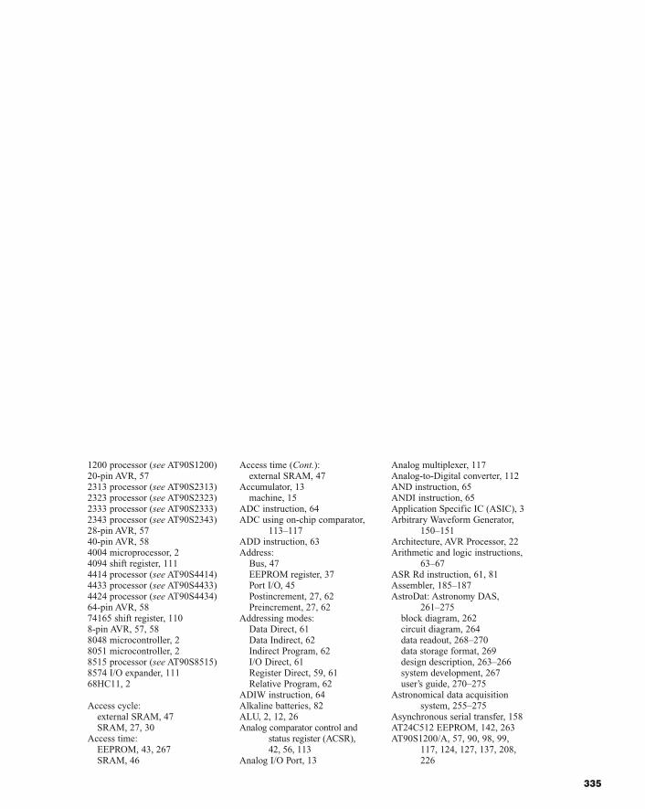
1200 processor (see AT90S1200)20-pin AVR, 572313 processor (see AT90S2313)2323 processor (see AT90S2323)2333 processor (see AT90S2333)2343 processor (see AT90S2343)28-pin AVR, 5740-pin AVR, 584004 microprocessor, 24094 shift register, 1114414 processor (see AT90S4414)4433 processor (see AT90S4433)4424 processor (see AT90S4434)64-pin AVR, 5874165 shift register, 1108-pin AVR, 57, 588048 microcontroller, 28051 microcontroller, 28515 processor (see AT90S8515)8574 I/O expander, 11168HC11, 2
Access cycle:external SRAM, 47SRAM, 27, 30
Access time:EEPROM, 43, 267SRAM, 46
Access time (Cont.):external SRAM, 47
Accumulator, 13machine, 15
ADC instruction, 64ADC using on-chip comparator,
113–117ADD instruction, 63Address:
Bus, 47EEPROM register, 37Port I/O, 45Postincrement, 27, 62Preincrement, 27, 62
Addressing modes:Data Direct, 61Data Indirect, 62Indirect Program, 62I/O Direct, 61Register Direct, 59, 61Relative Program, 62
ADIW instruction, 64Alkaline batteries, 82ALU, 2, 12, 26Analog comparator control and
status register (ACSR), 42, 56, 113
Analog I/O Port, 13
Analog multiplexer, 117Analog-to-Digital converter, 112AND instruction, 65ANDI instruction, 65Application Specific IC (ASIC), 3Arbitrary Waveform Generator,
150–151Architecture, AVR Processor, 22Arithmetic and logic instructions,
63–67ASR Rd instruction, 61, 81Assembler, 185–187AstroDat: Astronomy DAS,
261–275block diagram, 262circuit diagram, 264data readout, 268–270data storage format, 269design description, 263–266system development, 267user’s guide, 270–275
Astronomical data acquisition system, 255–275
Asynchronous serial transfer, 158AT24C512 EEPROM, 142, 263AT90S1200/A, 57, 90, 98, 99,
117, 124, 127, 137, 208,226
335
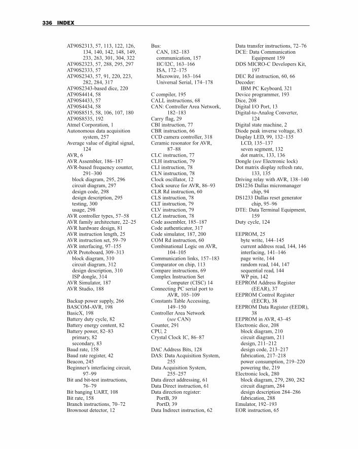
AT90S2313, 57, 113, 122, 126, 134, 140, 142, 148, 149,233, 263, 301, 304, 322
AT90S2323, 57, 288, 295, 297AT90S2333, 57AT90S2343, 57, 91, 220, 223,
282, 284, 317AT90S2343-based dice, 220AT90S4414, 58AT90S4433, 57AT90S4434, 58AT90S8515, 58, 106, 107, 180AT90S8535, 192Atmel Corporation, 1Autonomous data acquisition
system, 257Average value of digital signal,
124AVR, 6AVR Assembler, 186–187AVR-based frequency counter,
291–300block diagram, 295, 296circuit diagram, 297design code, 298design description, 295testing, 300usage, 298
AVR controller types, 57–58AVR family architecture, 22–25AVR hardware design, 81AVR instruction length, 25AVR instruction set, 59–79AVR interfacing, 97–155AVR Protoboard, 309–313
block diagram, 310circuit diagram, 312design description, 310ISP dongle, 314
AVR Simulator, 187AVR Studio, 188
Backup power supply, 266BASCOM-AVR, 198BasicX, 198Battery duty cycle, 82Battery energy content, 82Battery power, 82–83
primary, 82secondary, 83
Baud rate, 158Baud rate register, 42Beacon, 245Beginner’s interfacing circuit,
97–99Bit and bit-test instructions,
76–79Bit banging UART, 108Bit rate, 158Branch instructions, 70–72Brownout detector, 12
Bus:CAN, 182–183communication, 157IIC/I2C, 163–166ISA, 172–175Microwire, 163–164Universal Serial, 174–178
C compiler, 195CALL instructions, 68CAN: Controller Area Network,
182–183Carry flag, 29CBI instruction, 77CBR instruction, 66CCD camera controller, 318Ceramic resonator for AVR,
87–88CLC instruction, 77CLH instruction, 79CLI instruction, 78CLN instruction, 78Clock oscillator, 12Clock source for AVR, 86–93CLR Rd instruction, 60CLS instruction, 78CLT instruction, 79CLV instruction, 79CLZ instruction, 78Code assembler, 185–187Code authenticator, 317Code simulator, 187, 200COM Rd instruction, 60Combinational Logic on AVR,
104–105Communication links, 157–183Comparator on chip, 113Compare instructions, 69Complex Instruction Set
Computer (CISC) 14Connecting PC serial port to
AVR, 105–109Constants Table Accessing,
149–150Controller Area Network
(see CAN)Counter, 291CPU, 2Crystal Clock IC, 86–87
DAC Address Bits, 128DAS: Data Acquisition System,
255Data Acquisition System,
255–257Data direct addressing, 61Data Direct instruction, 61Data direction register:
PortB, 39PortD, 39
Data Indirect instruction, 62
Data transfer instructions, 72–76DCE: Data Communication
Equipment 159DDS MICRO-C Developers Kit,
197DEC Rd instruction, 60, 66Decoder:
IBM PC Keyboard, 321Device programmer, 193Dice, 208Digital I/O Port, 13Digital-to-Analog Converter,
124Digital state machine, 2Diode peak inverse voltage, 83Display LED, 99, 132–135
LCD, 135–137seven segment, 132dot matrix, 133, 136
Dongle (see Electronic lock)Dot matrix display refresh rate,
133, 135Driving relay with AVR, 138–140DS1236 Dallas micromanager
chip, 94DS1233 Dallas reset generator
chip, 95–96DTE: Data Terminal Equipment,
159Duty cycle, 124
EEPROM, 25byte write, 144–145current address read, 144, 146interfacing, 141–146page write, 144random read, 144, 147sequential read, 144WP pin, 142
EEPROM Address Register (EEAR), 37
EEPROM Control Register (EECR), 38
EEPROM Data Register (EEDR), 38
EEPROM in AVR, 43–45Electronic dice, 208
block diagram, 210circuit diagram, 211design, 211–212design code, 213–217fabrication, 217–218power consumption, 219–220powering the, 219
Electronic lock, 280block diagram, 279, 280, 282circuit diagram, 284design description 284–286fabrication, 288
Emulator, 192–193EOR instruction, 65
336 INDEX
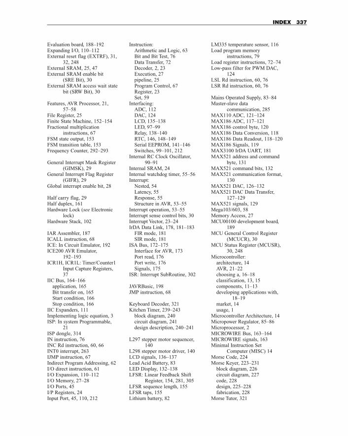
Evaluation board, 188–192Expanding I/O, 110–112External reset flag (EXTRF), 31,
32, 248External SRAM, 25, 47External SRAM enable bit
(SRE Bit), 30External SRAM access wait state
bit (SRW Bit), 30
Features, AVR Processor, 21, 57–58
File Register, 25Finite State Machine, 152–154Fractional multiplication
instructions, 67FSM state output, 153FSM transition table, 153Frequency Counter, 292–293
General Interrupt Mask Register (GIMSK), 29
General Interrupt Flag Register (GIFR), 29
Global interrupt enable bit, 28
Half carry flag, 29Half duplex, 161Hardware Lock (see Electronic
lock)Hardware Stack, 102
IAR Assembler, 187ICALL instruction, 68ICE: In Circuit Emulator, 192ICE200 AVR Emulator,
192–193ICR1H, ICR1L: Timer/Counter1
Input Capture Registers,37
IIC Bus, 164–166application, 165Bit transfer on, 165Start condition, 166Stop condition, 166
IIC Expanders, 111Implementing logic equation, 3ISP: In system Programmable,
21ISP dongle, 314IN instruction, 76INC Rd instruction, 60, 66INT0 interrupt, 263IJMP instruction, 67Indirect Program Addressing, 62I/O direct instruction, 61I/O Expansion, 110–112I/O Memory, 27–28I/O Ports, 45I/P Registers, 24Input Port, 45, 110, 212
Instruction:Arithmetic and Logic, 63Bit and Bit Test, 76Data Transfer, 72Decoder, 2, 23Execution, 27pipeline, 25Program Control, 67Register, 23Set, 59
Interfacing:ADC, 112DAC, 124LCD, 135–138LED, 97–99Relay, 138–140RTC, 146, 148–149Serial EEPROM, 141–146Switches, 99–101, 212
Internal RC Clock Oscillator, 90–91
Internal SRAM, 24Internal watchdog timer, 55–56Interrupt:
Nested, 54Latency, 55Response, 55Structure in AVR, 53–55
Interrupt operation, 53–55Interrupt sense control bits, 30Interrupt Vector, 23–24IrDA Data Link, 178, 181–183
FIR mode, 181SIR mode, 181
ISA Bus, 172–175Interface for AVR, 173Port read, 176Port write, 176Signals, 175
ISR: Interrupt SubRoutine, 302
JAVRBasic, 198JMP instruction, 68
Keyboard Decoder, 321Kitchen Timer, 239–243
block diagram, 240circuit diagram, 241design description, 240–241
L297 stepper motor sequencer, 140
L298 stepper motor driver, 140LCD signals, 136–137Lead Acid Battery, 83LED Display, 132–138LFSR: Linear Feedback Shift
Register, 154, 281, 305LFSR sequence length, 155LFSR taps, 155Lithium battery, 82
LM335 temperature sensor, 116Load program memory
instructions, 79Load register instructions, 72–74Low-pass filter for PWM DAC,
124LSL Rd instruction, 60, 76LSR Rd instruction, 60, 76
Mains Operated Supply, 83–84Master-slave data
communication, 285MAX110 ADC, 121–124MAX186 ADC, 117–121MAX186 control byte, 120MAX186 Data Conversion, 118MAX186 Data Readout, 118–120MAX186 Signals, 119MAX3100 IrDA UART, 181MAX521 address and command
byte, 131MAX521 command bits, 132MAX521 communication format,
130MAX521 DAC, 126–132MAX521 DAC Data Transfer,
127–129MAX521 signals, 129Mega103/603, 58Memory Access, 27MCU00100 development board,
189MCU General Control Register
(MCUCR), 30MCU Status Register (MCUSR),
30, 248Microcontroller:
architecture, 14AVR, 21–22choosing a, 16–18classification, 13, 15components, 11–13developing applications with,
18–19market, 14usage, 1
Microcontroller Architecture, 14Micropower Regulator, 85–86Microprocessor, 2MICROWIRE Bus, 163–164MICROWIRE signals, 163Minimal Instruction Set
Computer (MISC) 14Morse Code, 224Morse Keyer, 223–231
block diagram, 226circuit diagram, 227code, 228design, 225–228fabrication, 228
Morse Tutor, 321
INDEX 337
Motor speed ramping, 141, 144Motor stepper, 140MOV instructions, 72Multiple MAX521 in a single
bus, 129, 133Multiply instructions, 66–67Musical notes, 303Musical toy, 301–307
block diagram, 302circuit diagram, 304design code, 305–306fabrication, 303
NEG Rd instruction, 66Negative flag, 29Nickel cadmium cell, 83Nipper, 202NOP instruction, 79Nose plier, 202
OCR1AH, OCR1AL: Timer/Counter1 OutputCompare Register, 36
OCR1BH, OCR1BL: Timer/Counter1 OutputCompare Register, 36
On-chip UART, 58, 108OR instructions, 65Oscillator (see Clock source for
AVR)Out instruction, 76Output port, 45
Parallel port, 166–171control port address, 168data port address, 168signals, 171Status port address, 168
PCB: Printed Circuit Board, 200
Peak inverse voltage (PIV) for diode, 83
Period counter, 293–294PLD (Programmable Logic
Device), 3Point-to-point communication,
157Pointer register, 27POP instruction, 76Port:
I/O, 45PortB, 39PortD, 39
PortB data register (PORTB), 39
PortB input pins (PINB), 39PortD data register (PORTB),
39PortD input pins (PIND), 39Power down modes in AVR,
56–57, 247Power from Serial Port, 84–85
Power-on reset flag (PORF), 31, 32, 248
Power source, 81–86Power supply pitfalls, 290Primary batteries, 82Program addressing
Direct, 59–60Indirect, 62Relative, 62
Program control instructions, 67–72
Program memory, 12in AVR, 23
Programmer, 193Protoboard, 200Prototyping techniques, 199PUSH instruction, 76PWM: Pulse Width Modulation,
124PWM DAC, 124
Quartz crystal clock for AVR, 88–89
Quartz clock crystal for AVR, 90
R-2R ladder DAC, 124, 127Radio Beacon, 245
block diagram, 246circuit diagram, 251design description, 246–249operation flowchart, 250
RAM, 12Random Number Generator,
154–155RC clock oscillator, 91RC clock oscillator voltage
dependence, 91RCALL instruction, 68Reduced Instruction Set
Computer (RISC), 14Register direct instruction,
59–61Register file, 24, 25–26Register-memory machine, 15Register-register machine, 15–16Regulator:
Micropower (see Micropower Regulator)
Voltage (see Voltage Regulators)
Relative Program Addressing, 62Relay Driver, 138–140Reset, 12Reset circuit for AVR, 93–96Reset source, 30, 32Resonator (see Ceramic resonator
for AVR)RET instruction, 68RETI instruction, 68RJMP instruction, 67ROL Rd instruction, 60, 76ROR Rd instruction, 60, 76
RS-232:Connector pinout, 161Converter, 106handshake lines, 160Levels, 106, 109Line driver, 106, 161Port, 158–160
RS-422/423, 160–161RS-485, 161–163RTC: Real Time Clock, 13RZI: Return to Zero, 181
Sample and hold amplifier, 117SBI instruction, 77SBR instruction, 66Secondary batteries, 83Set instructions, 77–79SER Rd instruction, 60Serial ADC, 117Serial port, 13, 105Seven Segment Display, 132Shift Register for I/O expansion
110–111Signal bounce, 100Sign flag, 29SimmStick, 194–195Simulator, 187, 200Skip instructions, 69–70Sleep enable bit (SE), 30SLEEP instruction, 79Sleep mode bit (SM), 30Smart Card, 1SniffStick, 257–261
block diagram, 258circuit diagram, 259data readout, 258–260readout port, 258usage, 260
Software driven UART, 108Solder Iron, 202SPI Bus, 163–164SPI control register, 40SPI I/O data register, 39SPI status register, 39SRAM in AVR, 46SRAM Interface, 46–48Stack, 101Stack operation, 53, 101Stack machine, 15Stack pointer, 101Stack pointer register (SP), 29State machine, 152–154STATUS register (SREG), 28–29,
305Stepper motor interface, 140Steps for prototyping,
203–205STK200 board, 189–192STK300 board, 192Store instructions, 74–75Subtract instructions, 64–65SWAP Rd instruction, 61, 77
338 INDEX
Swipe Card, 320Switch-case implementation,
150–152Switch debounce, 100–101Switch interfacing with AVR,
99–101
Temperature logger, 318Temperature sensor, 116, 318Terminal emulation program, 106Timer, 13Timer/Counter0 control register
(TCCR0), 31Timer/Counter0 register
(TCNT0), 31Timer/Counter1
(TCNT1H/TCNT1L), 34Timer/Counter1 control register A
(TCCR1A), 32Timer/Counter1 control register B
(TCCR1B), 33Timer/Counter1 Output compare
register A (OCR1AH,OCR1AL), 35
Timer/Counter1 Output compare register B (OCR1BH,OCR1BL), 36
Timer/Counter1 Input compare reg-ister (ICR1H, ICR1L), 37
Timer0 interrupt, 228, 305Timer1 interrupt, 263Timer0 ISR, 305Timer operation in AVR,
47–49Timing diagram convention,
6–9Tiny10, 58Tiny12, 58Tiny13, 58Tiny22, 58, 91, 223, 248, 282,
284Tiny22 for radio beacon, 249TMS1000 Microcontroller, 2Tools for prototyping, 202–203TST Rd instruction, 60Tweezers, 202Two’s complement flag, 29
UART baud rate register, 42UART control register, 41UART I/O data register, 40UART operation in AVR,
49–53UART status register, 40ULN2003 darlington array, 138,
141USB: Universal Serial Bus,
174–178
USB: Universal Serial Bus (Cont.):
connectivity, 177devices, 178host, 177topology, 179
Voltage reference source, 117Voltage regulators, 85–86Voltmeter, 233
block diagram, 234circuit diagram, 236
Wall plug-in transformer, 83Watchdog control register
(WDTCR), 37Watchdog timer, 13Watchdog timer prescale select,
38WDR instruction, 79Wire stripper, 202
X register, 66, 73
Y register, 66, 73
Z register, 66, 73Zero flag, 29Zinc chloride batteries, 82
INDEX 339

This page intentionally left blank.

About the AuthorDhananjay V. Gadre is a scientific officer with the Instrumentation Program of the Inter-University Centre for Astronomy and Astrophysics (IUCAA) in Pune, India. He has aM.Engr. from the University of Idaho and a M.Sc. from the University of Delhi. Dhananjay’sinterests include computer architecture, communication networks, hardware-software co-design, programmable logic devices and Hardware Description Languages. He is a licensedradio amateur (VU2NOX). He has written articles for a number of electronics magazines,including Electronics World. He is also the author of Programming the Parallel Port:Interfacing the PC for Data Acquisition and Process Control (R&D Books, 1998).
Copyright 2001 The McGraw-Hill Companies, Inc. Click Here for Terms of Use.


