95
Analog Electronics - I An Introduction Mr. Zeeshan Ali, Asst. Professor Semester III B.E. Electronic & Telecommunication Anjuman-I-Islam’s Kalsekar Technical Campus New Panvel - 410206
| Date post: | 10-Mar-2023 |
| Category: |
Documents |
| Upload: | khangminh22 |
| View: | 0 times |
| Download: | 0 times |

Analog Electronics - I
An Introduction
Mr. Zeeshan Ali, Asst. Professor
Semester III
B.E. Electronic & Telecommunication
Anjuman-I-Islam’s Kalsekar Technical Campus
New Panvel - 410206
Anjuman-I-Islam’s Kalsekar Technical Campus, New Panvel
ANALOG ELECTRONICS- I
SR. NO.
1.
2.
3.
4.
5.
NAME OF THE TOPIC
Field Effect Transistor
Biasing of BJT’S
Biasing of FET’S and MOSFET’S
Small Signal Analysis Of BJTS
Small Signal Analysis of FETS
6. High Frequency Response of FETS and BJTS
Page | 1
Anjuman-I-Islam’s Kalsekar Technical Campus, New Panvel
Topic 1 FIELD EFFECT TRANSISTORS
1.1 INTRODUCTION
The field-effect transistor (FET) is a three-terminal device used for a variety of
applications that match, to a large extent. Although there are important
differences between the two types of devices, there are also many similarities.
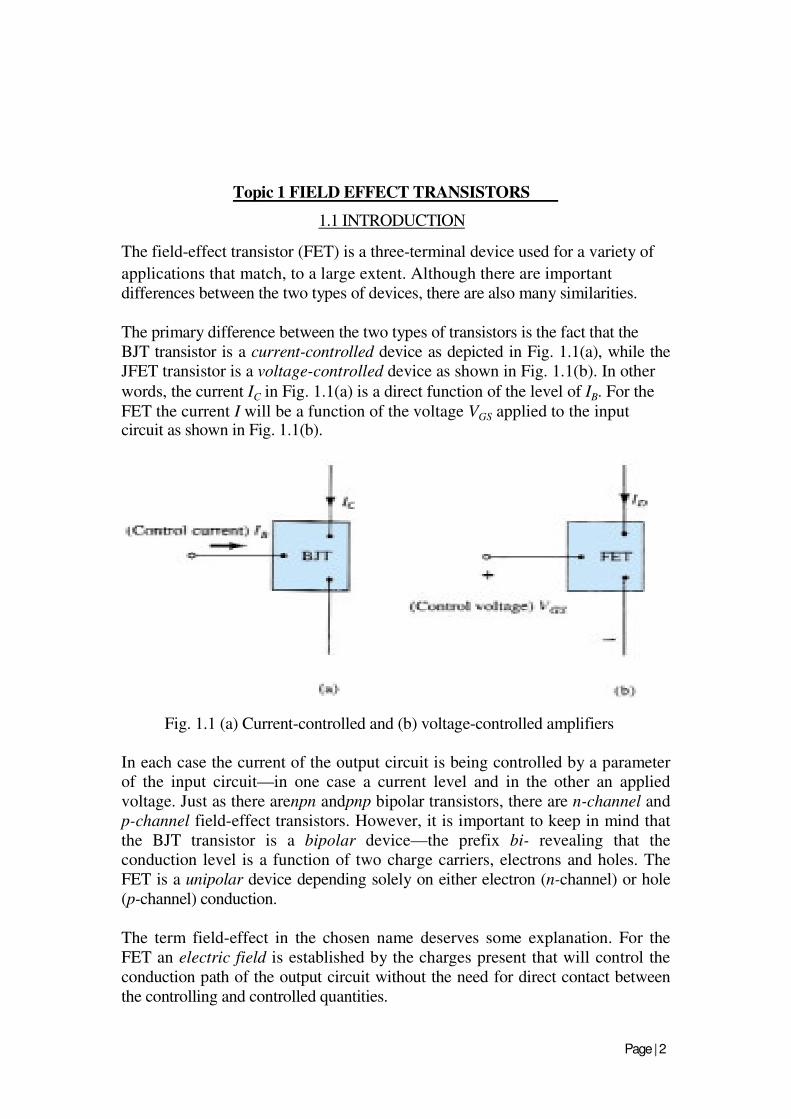
The primary difference between the two types of transistors is the fact that the
BJT transistor is a current-controlled device as depicted in Fig. 1.1(a), while the
JFET transistor is a voltage-controlled device as shown in Fig. 1.1(b). In other
words, the current IC in Fig. 1.1(a) is a direct function of the level of IB. For the
FET the current I will be a function of the voltage VGS applied to the input circuit as shown in Fig. 1.1(b).
Fig. 1.1 (a) Current-controlled and (b) voltage-controlled amplifiers
In each case the current of the output circuit is being controlled by a parameter
of the input circuit—in one case a current level and in the other an applied
voltage. Just as there arenpn andpnp bipolar transistors, there are n-channel and
p-channel field-effect transistors. However, it is important to keep in mind that
the BJT transistor is a bipolar device—the prefix bi- revealing that the
conduction level is a function of two charge carriers, electrons and holes. The
FET is a unipolar device depending solely on either electron (n-channel) or hole
(p-channel) conduction.
The term field-effect in the chosen name deserves some explanation. For the
FET an electric field is established by the charges present that will control the
conduction path of the output circuit without the need for direct contact between
the controlling and controlled quantities.
Page | 2
Anjuman-I-Islam’s Kalsekar Technical Campus, New Panvel
One of the most important characteristics of the FET is its high input
impedance. At a level of 1 to several hundred mega ohms it far exceeds the
typical input resistance levels of the BJT transistor configurations—a very
important characteristic in the design of linear ac amplifier systems. On the
other hand, the BJT transistor has a much higher sensitivity to changes in the
applied signal. In other words, the variation in output current is typically a great
deal more for BJTs than FETs for the same change in applied voltage. For this
reason, typical ac voltage gains for BJT amplifiers are a great deal more than for
FETs. In general, FETs are more temperature stable than BJTs, and FETs are
usually smaller in construction than BJTs, making them particularly useful in
integrated-circuit (IC) chips. The construction characteristics of some FETs,
however, can make them more sensitive to handling than BJTs.
Two types of FETs are there: the junction field-effect transistor (JFET) and the metal-oxide-semiconductor field-effect transistor (MOSFET).
The MOSFET category is further broken down into depletion and enhancement
types. The MOSFET transistor has become one of the most important devices
used in the design and construction of integrated circuits for digital computers.
Its thermal stability and other general characteristics make it extremely popular
in computer circuit design.
1.2 CONSTRUCTION AND CHARACTERISTICS OF JFETs
The JFET is a three-terminal device with one terminal capable of controlling the
current between the other two.
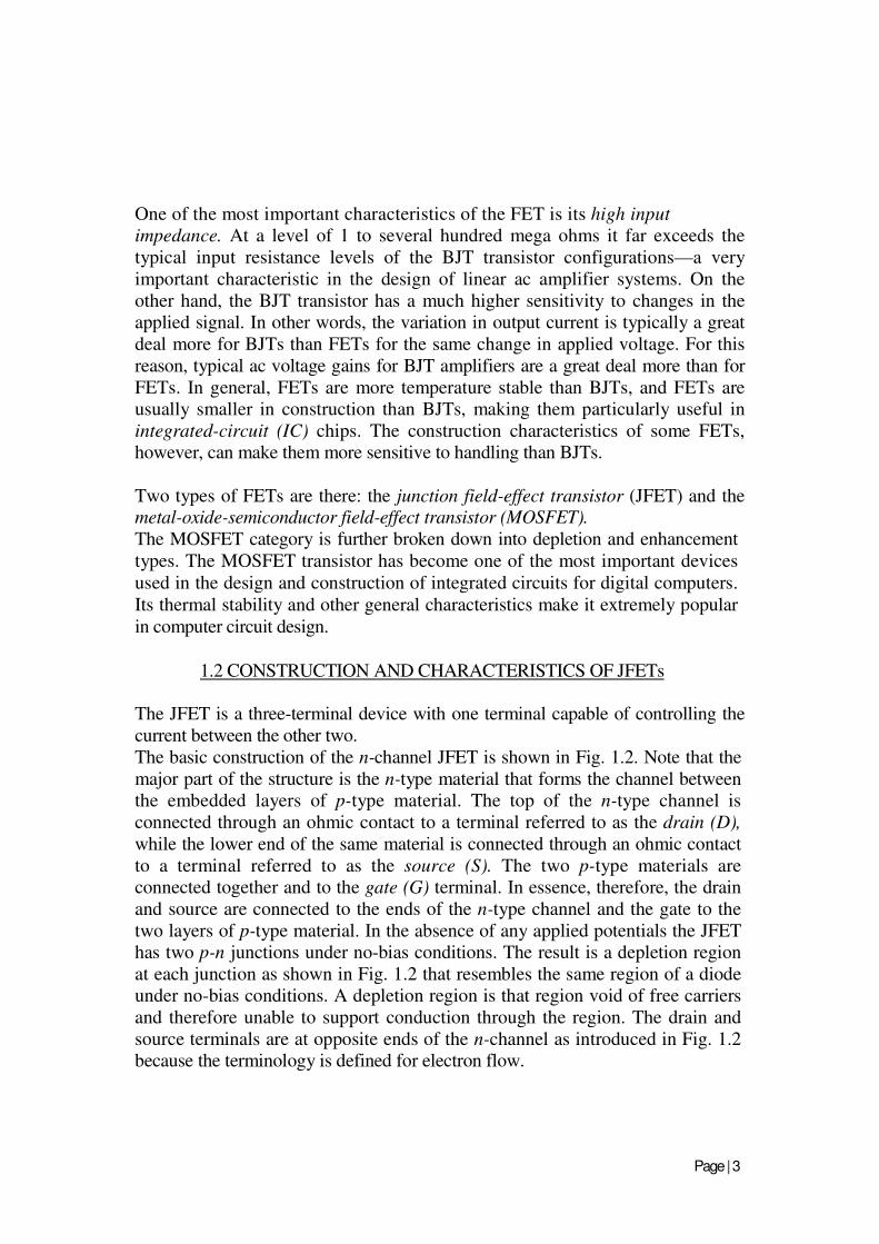
The basic construction of the n-channel JFET is shown in Fig. 1.2. Note that the
major part of the structure is the n-type material that forms the channel between
the embedded layers of p-type material. The top of the n-type channel is
connected through an ohmic contact to a terminal referred to as the drain (D),
while the lower end of the same material is connected through an ohmic contact
to a terminal referred to as the source (S). The two p-type materials are
connected together and to the gate (G) terminal. In essence, therefore, the drain
and source are connected to the ends of the n-type channel and the gate to the
two layers of p-type material. In the absence of any applied potentials the JFET
has two p-n junctions under no-bias conditions. The result is a depletion region
at each junction as shown in Fig. 1.2 that resembles the same region of a diode
under no-bias conditions. A depletion region is that region void of free carriers
and therefore unable to support conduction through the region. The drain and
source terminals are at opposite ends of the n-channel as introduced in Fig. 1.2
because the terminology is defined for electron flow.
Page | 3
Anjuman-I-Islam’s Kalsekar Technical Campus, New Panvel
Fig 1.2 Junction field-effect transistor (JFET)
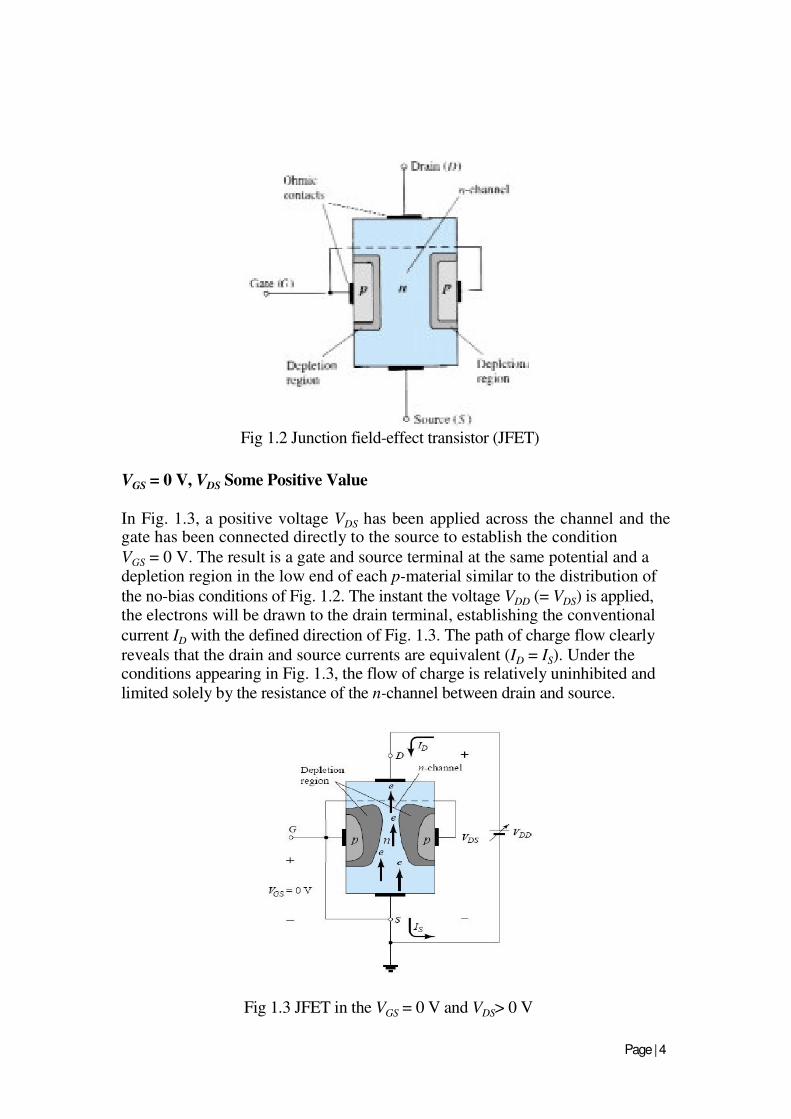
VGS = 0 V, VDS Some Positive Value
In Fig. 1.3, a positive voltage VDS has been applied across the channel and the gate has been connected directly to the source to establish the condition
VGS = 0 V. The result is a gate and source terminal at the same potential and a depletion region in the low end of each p-material similar to the distribution of
the no-bias conditions of Fig. 1.2. The instant the voltage VDD (= VDS) is applied, the electrons will be drawn to the drain terminal, establishing the conventional
current ID with the defined direction of Fig. 1.3. The path of charge flow clearly
reveals that the drain and source currents are equivalent (ID = IS). Under the conditions appearing in Fig. 1.3, the flow of charge is relatively uninhibited and
limited solely by the resistance of the n-channel between drain and source.
Fig 1.3 JFET in the VGS = 0 V and VDS> 0 V
Page | 4
Anjuman-I-Islam’s Kalsekar Technical Campus, New Panvel
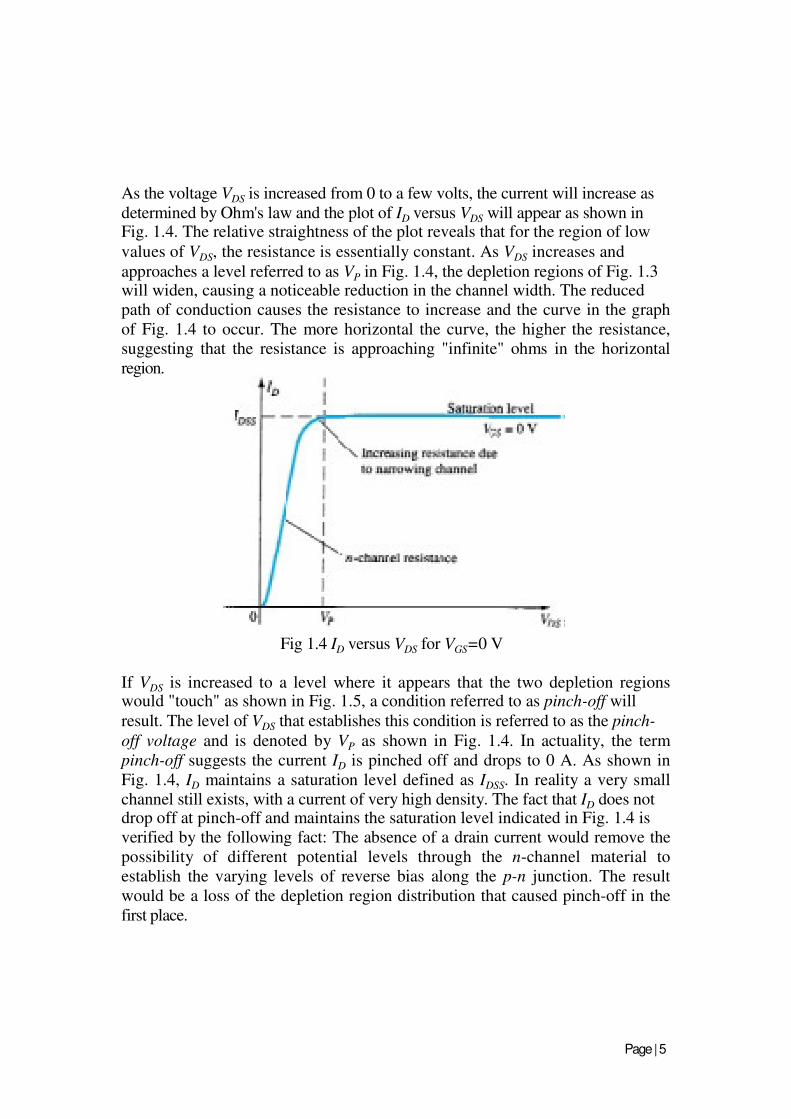
As the voltage VDS is increased from 0 to a few volts, the current will increase as
determined by Ohm's law and the plot of ID versus VDS will appear as shown in Fig. 1.4. The relative straightness of the plot reveals that for the region of low
values of VDS, the resistance is essentially constant. As VDS increases and
approaches a level referred to as VP in Fig. 1.4, the depletion regions of Fig. 1.3 will widen, causing a noticeable reduction in the channel width. The reduced
path of conduction causes the resistance to increase and the curve in the graph
of Fig. 1.4 to occur. The more horizontal the curve, the higher the resistance,
suggesting that the resistance is approaching "infinite" ohms in the horizontal
region.
Fig 1.4 ID versus VDS for VGS=0 V
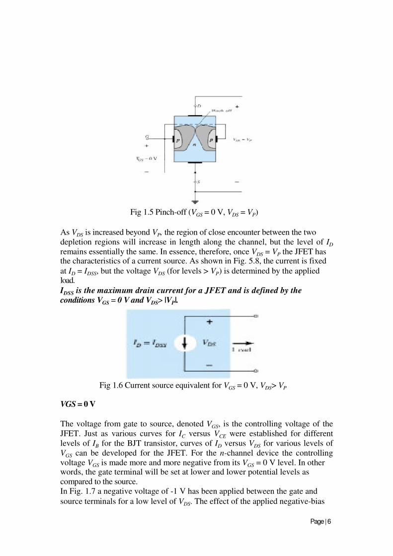
If VDS is increased to a level where it appears that the two depletion regions would "touch" as shown in Fig. 1.5, a condition referred to as pinch-off will
result. The level of VDS that establishes this condition is referred to as the pinch-
off voltage and is denoted by VP as shown in Fig. 1.4. In actuality, the term
pinch-off suggests the current ID is pinched off and drops to 0 A. As shown in
Fig. 1.4, ID maintains a saturation level defined as IDSS. In reality a very small
channel still exists, with a current of very high density. The fact that ID does not drop off at pinch-off and maintains the saturation level indicated in Fig. 1.4 is
verified by the following fact: The absence of a drain current would remove the
possibility of different potential levels through the n-channel material to
establish the varying levels of reverse bias along the p-n junction. The result
would be a loss of the depletion region distribution that caused pinch-off in the
first place.
Page | 5
Anjuman-I-Islam’s Kalsekar Technical Campus, New Panvel
Fig 1.5 Pinch-off (VGS = 0 V, VDS = VP)
As VDS is increased beyond VP, the region of close encounter between the two
depletion regions will increase in length along the channel, but the level of ID
remains essentially the same. In essence, therefore, once VDS = VP the JFET has the characteristics of a current source. As shown in Fig. 5.8, the current is fixed
at ID = IDSS, but the voltage VDS (for levels > VP) is determined by the applied load.
IDSS is the maximum drain current for a JFET and is defined by the
conditions VGS = 0 V and VDS> |VP|.
Fig 1.6 Current source equivalent for VGS = 0 V, VDS> VP
VGS = 0 V
The voltage from gate to source, denoted VGS, is the controlling voltage of the
JFET. Just as various curves for IC versus VCE were established for different
levels of IB for the BJT transistor, curves of ID versus VDS for various levels of
VGS can be developed for the JFET. For the n-channel device the controlling
voltage VGS is made more and more negative from its VGS = 0 V level. In other words, the gate terminal will be set at lower and lower potential levels as
compared to the source.
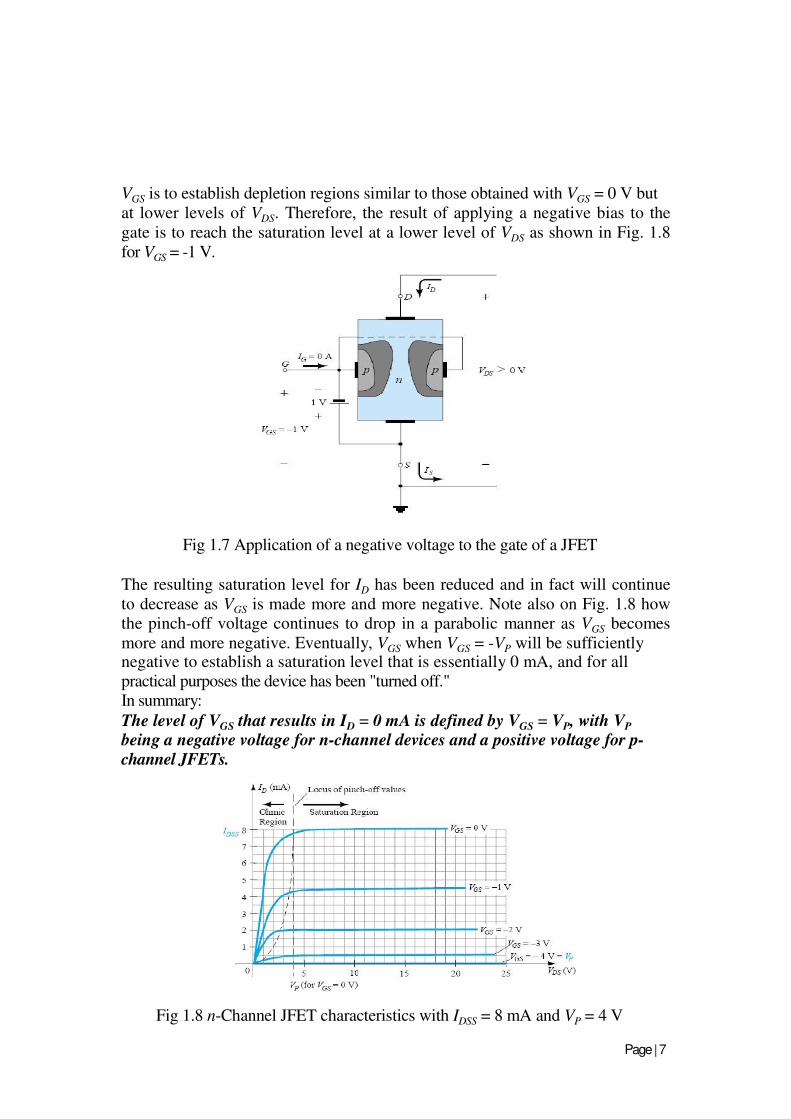
In Fig. 1.7 a negative voltage of -1 V has been applied between the gate and
source terminals for a low level of VDS. The effect of the applied negative-bias
Page | 6
Anjuman-I-Islam’s Kalsekar Technical Campus, New Panvel
VGS is to establish depletion regions similar to those obtained with VGS = 0 V but
at lower levels of VDS. Therefore, the result of applying a negative bias to the
gate is to reach the saturation level at a lower level of VDS as shown in Fig. 1.8
for VGS = -1 V.
Fig 1.7 Application of a negative voltage to the gate of a JFET
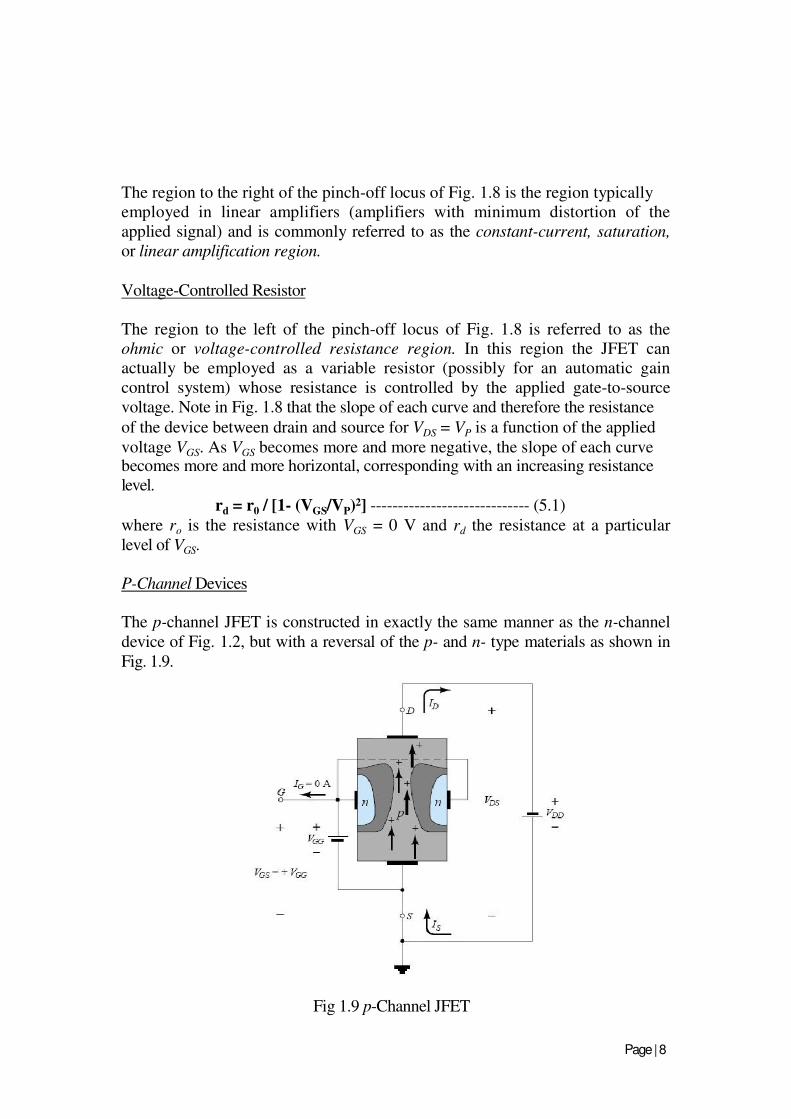
The resulting saturation level for ID has been reduced and in fact will continue
to decrease as VGS is made more and more negative. Note also on Fig. 1.8 how
the pinch-off voltage continues to drop in a parabolic manner as VGS becomes
more and more negative. Eventually, VGS when VGS = -VP will be sufficiently negative to establish a saturation level that is essentially 0 mA, and for all
practical purposes the device has been "turned off."
In summary:
The level of VGS that results in ID = 0 mA is defined by VGS = VP, with VP
being a negative voltage for n-channel devices and a positive voltage for p-
channel JFETs.
Fig 1.8 n-Channel JFET characteristics with IDSS = 8 mA and VP = 4 V
Page | 7
Anjuman-I-Islam’s Kalsekar Technical Campus, New Panvel
The region to the right of the pinch-off locus of Fig. 1.8 is the region typically
employed in linear amplifiers (amplifiers with minimum distortion of the
applied signal) and is commonly referred to as the constant-current, saturation,
or linear amplification region.
Voltage-Controlled Resistor
The region to the left of the pinch-off locus of Fig. 1.8 is referred to as the
ohmic or voltage-controlled resistance region. In this region the JFET can
actually be employed as a variable resistor (possibly for an automatic gain
control system) whose resistance is controlled by the applied gate-to-source
voltage. Note in Fig. 1.8 that the slope of each curve and therefore the resistance
of the device between drain and source for VDS = VP is a function of the applied
voltage VGS. As VGS becomes more and more negative, the slope of each curve becomes more and more horizontal, corresponding with an increasing resistance
level.
rd = r0 / [1- (VGS/VP)2] ----------------------------- (5.1)
where ro is the resistance with VGS = 0 V and rd the resistance at a particular
level of VGS.
P-Channel Devices
The p-channel JFET is constructed in exactly the same manner as the n-channel
device of Fig. 1.2, but with a reversal of the p- and n- type materials as shown in
Fig. 1.9.
Fig 1.9 p-Channel JFET
Page | 8
Anjuman-I-Islam’s Kalsekar Technical Campus, New Panvel
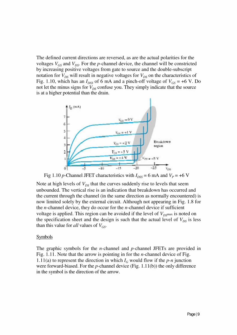
The defined current directions are reversed, as are the actual polarities for the
voltages VGS and VDS. For the p-channel device, the channel will be constricted by increasing positive voltages from gate to source and the double-subscript
notation for VDS will result in negative voltages for VDS on the characteristics of
Fig. 1.10, which has an IDSS of 6 mA and a pinch-off voltage of VGS = +6 V. Do
not let the minus signs for VDS confuse you. They simply indicate that the source is at a higher potential than the drain.
Fig 1.10 p-Channel JFET characteristics with IDSS = 6 mA and VP = +6 V
Note at high levels of VDS that the curves suddenly rise to levels that seem
unbounded. The vertical rise is an indication that breakdown has occurred and
the current through the channel (in the same direction as normally encountered) is
now limited solely by the external circuit. Although not appearing in Fig. 1.8 for
the n-channel device, they do occur for the n-channel device if sufficient
voltage is applied. This region can be avoided if the level of VDSmax is noted on
the specification sheet and the design is such that the actual level of VDS is less
than this value for all values of VGS.
Symbols
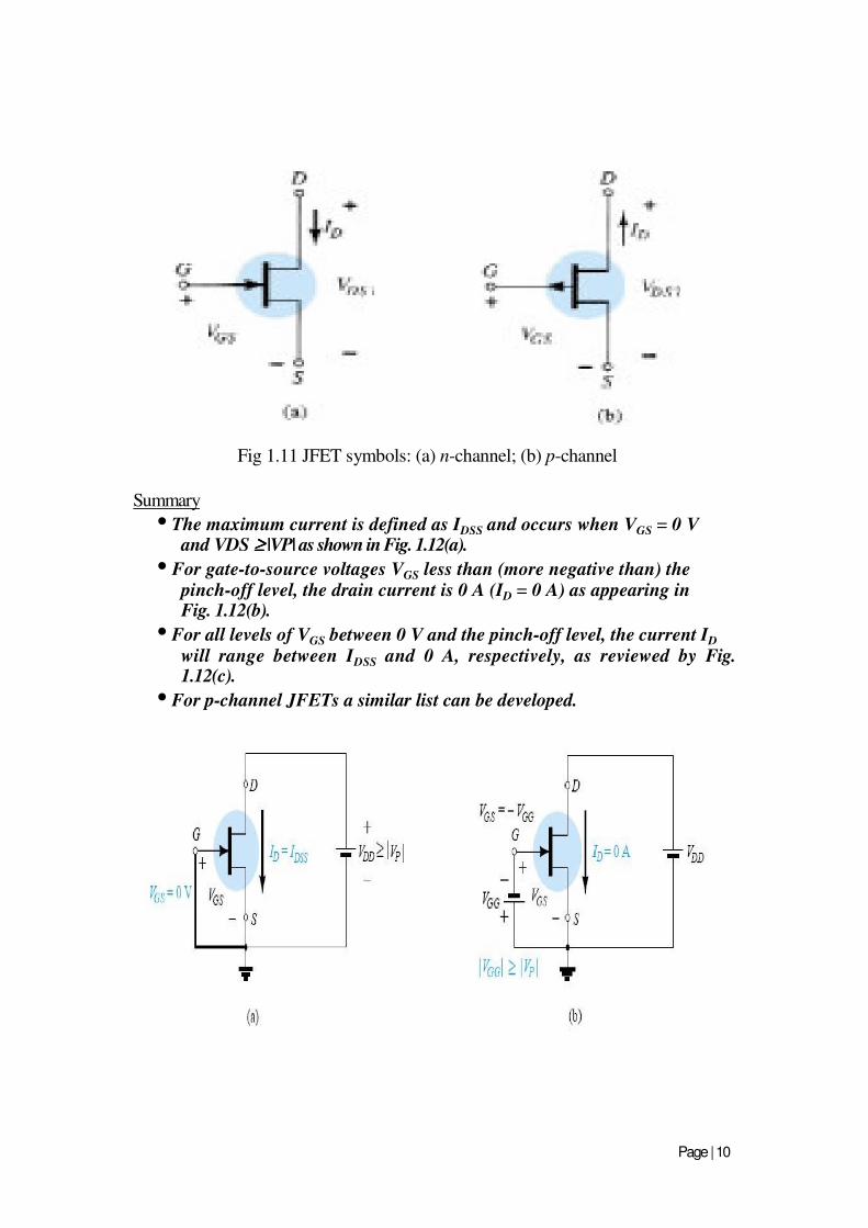
The graphic symbols for the n-channel and p-channel JFETs are provided in
Fig. 1.11. Note that the arrow is pointing in for the n-channel device of Fig.
1.11(a) to represent the direction in which IG would flow if the p-n junction were forward-biased. For the p-channel device (Fig. 1.11(b)) the only difference in the symbol is the direction of the arrow.
Page | 9
Anjuman-I-Islam’s Kalsekar Technical Campus, New Panvel
Fig 1.11 JFET symbols: (a) n-channel; (b) p-channel
Summary
• The maximum current is defined as IDSS and occurs when VGS = 0 V and VDS ≥≥≥≥ |VP| as shown in Fig. 1.12(a).
• For gate-to-source voltages VGS less than (more negative than) the pinch-off level, the drain current is 0 A (ID = 0 A) as appearing in Fig. 1.12(b).
• For all levels of VGS between 0 V and the pinch-off level, the current ID
will range between IDSS and 0 A, respectively, as reviewed by Fig. 1.12(c).
• For p-channel JFETs a similar list can be developed.
Page | 10
Anjuman-I-Islam’s Kalsekar Technical Campus, New Panvel
Fig 1.12 (a) VGS =0 V, ID = IDSS; (b) cutoff (ID = 0 A) VGS less than the pinch-off
level; (c) ID exists between 0 A and IDSS for VGS less than or equal to 0 V and greater than the pinch-off level.
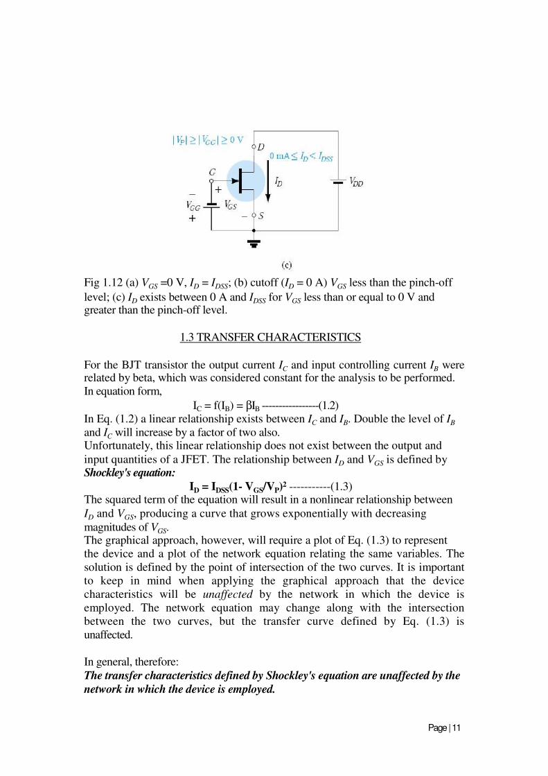
1.3 TRANSFER CHARACTERISTICS
For the BJT transistor the output current IC and input controlling current IB were related by beta, which was considered constant for the analysis to be performed.
In equation form,
IC = f(IB) = βIB -----------------(1.2) In Eq. (1.2) a linear relationship exists between IC and IB. Double the level of IB
and IC will increase by a factor of two also. Unfortunately, this linear relationship does not exist between the output and
input quantities of a JFET. The relationship between ID and VGS is defined by Shockley's equation:
ID = IDSS(1- VGS/VP)2 -----------(1.3) The squared term of the equation will result in a nonlinear relationship between
ID and VGS, producing a curve that grows exponentially with decreasing
magnitudes of VGS. The graphical approach, however, will require a plot of Eq. (1.3) to represent
the device and a plot of the network equation relating the same variables. The
solution is defined by the point of intersection of the two curves. It is important
to keep in mind when applying the graphical approach that the device
characteristics will be unaffected by the network in which the device is
employed. The network equation may change along with the intersection
between the two curves, but the transfer curve defined by Eq. (1.3) is
unaffected.
In general, therefore:
The transfer characteristics defined by Shockley's equation are unaffected by the
network in which the device is employed.
Page | 11
Anjuman-I-Islam’s Kalsekar Technical Campus, New Panvel
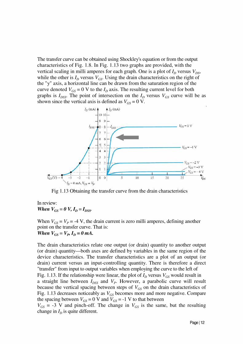
The transfer curve can be obtained using Shockley's equation or from the output
characteristics of Fig. 1.8. In Fig. 1.13 two graphs are provided, with the
vertical scaling in milli amperes for each graph. One is a plot of ID versus VDS,
while the other is ID versus VGS. Using the drain characteristics on the right of the "y" axis, a horizontal line can be drawn from the saturation region of the
curve denoted VGS = 0 V to the ID axis. The resulting current level for both
graphs is IDSS. The point of intersection on the ID versus VGS curve will be as
shown since the vertical axis is defined as VGS = 0 V.
Fig 1.13 Obtaining the transfer curve from the drain characteristics
In review:
When VGS = 0 V, ID = IDSS.
When VGS = VP = -4 V, the drain current is zero milli amperes, defining another point on the transfer curve. That is:
When VGS = VP, ID = 0 mA. The drain characteristics relate one output (or drain) quantity to another output
(or drain) quantity—both axes are defined by variables in the same region of the
device characteristics. The transfer characteristics are a plot of an output (or
drain) current versus an input-controlling quantity. There is therefore a direct
"transfer" from input to output variables when employing the curve to the left of
Fig. 1.13. If the relationship were linear, the plot of ID versus VGS would result in
a straight line between IDSS and VP. However, a parabolic curve will result
because the vertical spacing between steps of VGS on the drain characteristics of
Fig. 1.13 decreases noticeably as VGS becomes more and more negative. Compare
the spacing between VGS = 0 V and VGS = -1 V to that between
VGS = -3 V and pinch-off. The change in VGS is the same, but the resulting
change in ID is quite different.
Page | 12
Anjuman-I-Islam’s Kalsekar Technical Campus, New Panvel
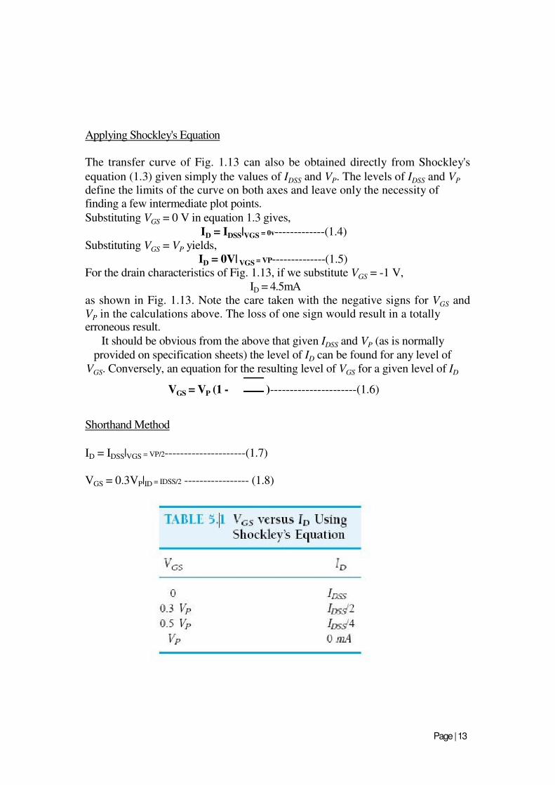
Applying Shockley's Equation
The transfer curve of Fig. 1.13 can also be obtained directly from Shockley's
equation (1.3) given simply the values of IDSS and VP. The levels of IDSS and VP
define the limits of the curve on both axes and leave only the necessity of finding a few intermediate plot points.
Substituting VGS = 0 V in equation 1.3 gives,
ID = IDSS|VGS = 0v-------------(1.4)
Substituting VGS = VP yields,
ID = 0V| VGS = VP--------------(1.5)
For the drain characteristics of Fig. 1.13, if we substitute VGS = -1 V,
ID = 4.5mA
as shown in Fig. 1.13. Note the care taken with the negative signs for VGS and
VP in the calculations above. The loss of one sign would result in a totally erroneous result.
It should be obvious from the above that given IDSS and VP (as is normally
provided on specification sheets) the level of ID can be found for any level of
VGS. Conversely, an equation for the resulting level of VGS for a given level of ID
VGS = VP (1 - )----------------------(1.6)
Shorthand Method
ID = IDSS|VGS = VP/2---------------------(1.7)
VGS = 0.3VP|ID = IDSS/2 ----------------- (1.8)
Page | 13
Anjuman-I-Islam’s Kalsekar Technical Campus, New Panvel
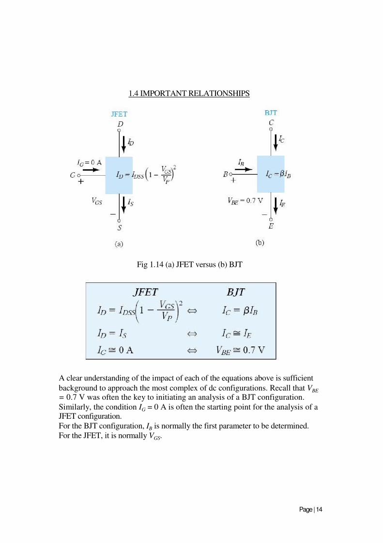
1.4 IMPORTANT RELATIONSHIPS
Fig 1.14 (a) JFET versus (b) BJT
A clear understanding of the impact of each of the equations above is sufficient
background to approach the most complex of dc configurations. Recall that VBE
= 0.7 V was often the key to initiating an analysis of a BJT configuration.
Similarly, the condition IG = 0 A is often the starting point for the analysis of a JFET configuration.
For the BJT configuration, IB is normally the first parameter to be determined.
For the JFET, it is normally VGS.
Page | 14
Anjuman-I-Islam’s Kalsekar Technical Campus, New Panvel
1.5 DEPLETION-TYPE MOSFET
There are two types of FETs: JFETs and MOSFETs. MOSFETs are further
broken down into depletion type and enhancement type. The terms depletion
and enhancement define their basic mode of operation, while the label
MOSFET stands for metal-oxide-semiconductor-field-effect transistor.
thedepletion-type MOSFET, which happens to have characteristics similar to
those
of a JFET between cut-off and saturation at IDSS but then has the added feature
of characteristics that extend into the region of opposite polarity for VGS.
Basic Construction
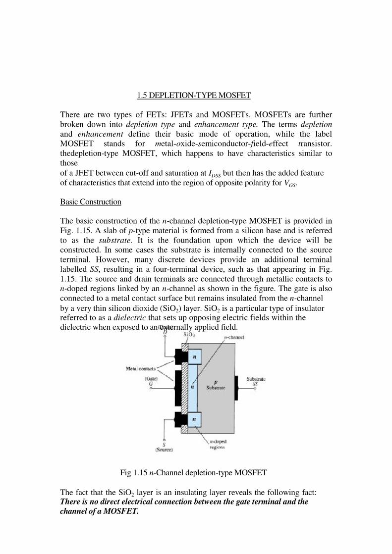
The basic construction of the n-channel depletion-type MOSFET is provided in
Fig. 1.15. A slab of p-type material is formed from a silicon base and is referred
to as the substrate. It is the foundation upon which the device will be
constructed. In some cases the substrate is internally connected to the source
terminal. However, many discrete devices provide an additional terminal
labelled SS, resulting in a four-terminal device, such as that appearing in Fig.
1.15. The source and drain terminals are connected through metallic contacts to
n-doped regions linked by an n-channel as shown in the figure. The gate is also
connected to a metal contact surface but remains insulated from the n-channel
by a very thin silicon dioxide (SiO2) layer. SiO2 is a particular type of insulator referred to as a dielectric that sets up opposing electric fields within the dielectric when exposed to an externally applied field.
Fig 1.15 n-Channel depletion-type MOSFET
The fact that the SiO2 layer is an insulating layer reveals the following fact: There is no direct electrical connection between the gate terminal and the channel of a MOSFET.

Anjuman-I-Islam’s Kalsekar Technical Campus, New Panvel
Page | 15
Anjuman-I-Islam’s Kalsekar Technical Campus, New Panvel
In addition:
It is the insulating layer of SiO2 in the MOSFET construction that accounts for the very desirable high input impedance of the device. In fact, the input resistance of a MOSFET is often that of the typical JFET, even
though the input impedance of most JFETs is sufficiently high for most
applications. The very high input impedance continues to fully support the fact
that the gate current (IG) is essentially zero amperes for dc-biased configurations. The reason for the label metal-oxide-semiconductor FET is now fairly obvious: metal for the drain, source, and gate connections to the proper
surface—in particular, the gate terminal and the control to be offered by the
surface area of the contact, the oxide for the silicon dioxide insulating layer, and
the semiconductor for the basic structure on which the n- and p-type regions are
diffused. The insulating layer between the gate and channel has resulted in
another name for the device: insulated gate FET or IGFET, although this label
is used less and less in current literature.
Basic Operation and Characteristics
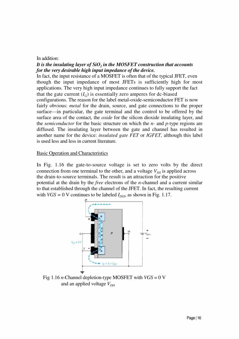
In Fig. 1.16 the gate-to-source voltage is set to zero volts by the direct
connection from one terminal to the other, and a voltage VDS is applied across the drain-to-source terminals. The result is an attraction for the positive
potential at the drain by the free electrons of the n-channel and a current similar
to that established through the channel of the JFET. In fact, the resulting current
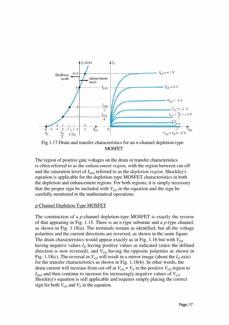
with VGS = 0 V continues to be labeled IDSS, as shown in Fig. 1.17.
Fig 1.16 n-Channel depletion-type MOSFET with VGS = 0 V
and an applied voltage VDD
Page | 16
Anjuman-I-Islam’s Kalsekar Technical Campus, New Panvel
Fig 1.17 Drain and transfer characteristics for an n-channel depletion-type
MOSFET
The region of positive gate voltages on the drain or transfer characteristics
is often referred to as the enhancement region, with the region between cut-off
and the saturation level of IDSS referred to as the depletion region. Shockley's equation is applicable for the depletion-type MOSFET characteristics in both
the depletion and enhancement regions. For both regions, it is simply necessary
that the proper sign be included with VGS in the equation and the sign be carefully monitored in the mathematical operations.
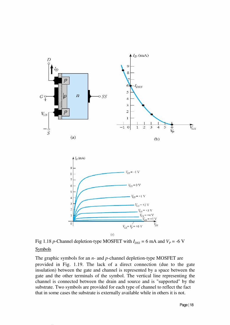
p-Channel Depletion-Type MOSFET
The construction of a p-channel depletion-type MOSFET is exactly the reverse
of that appearing in Fig. 1.15. There is an n-type substrate and a p-type channel,
as shown in Fig. 1.18(a). The terminals remain as identified, but all the voltage
polarities and the current directions are reversed, as shown in the same figure.
The drain characteristics would appear exactly as in Fig. 1.16 but with VDS
having negative values ID having positive values as indicated (since the defined
direction is now reversed), and VGS having the opposite polarities as shown in
Fig. 1.18(c). The reversal in VGS will result in a mirror image (about the ID axis) for the transfer characteristics as shown in Fig. 1.18(b). In other words, the
drain current will increase from cut-off at VGS = VP in the positive VGS region to
IDSS and then continue to increase for increasingly negative values of VGS. Shockley's equation is still applicable and requires simply placing the correct
sign for both VGS and VP in the equation.
Page | 17
Anjuman-I-Islam’s Kalsekar Technical Campus, New Panvel
Fig 1.18 p-Channel depletion-type MOSFET with IDSS = 6 mA and VP = -6 V
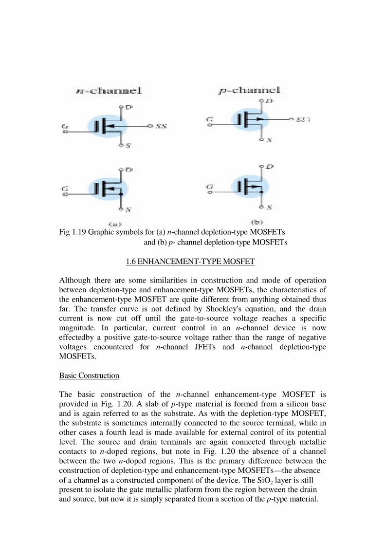
Symbols
The graphic symbols for an n- and p-channel depletion-type MOSFET are
provided in Fig. 1.19. The lack of a direct connection (due to the gate
insulation) between the gate and channel is represented by a space between the
gate and the other terminals of the symbol. The vertical line representing the
channel is connected between the drain and source and is "supported" by the
substrate. Two symbols are provided for each type of channel to reflect the fact
that in some cases the substrate is externally available while in others it is not.
Page | 18
Anjuman-I-Islam’s Kalsekar Technical Campus, New Panvel
Fig 1.19 Graphic symbols for (a) n-channel depletion-type MOSFETs
and (b) p- channel depletion-type MOSFETs
1.6 ENHANCEMENT-TYPE MOSFET
Although there are some similarities in construction and mode of operation
between depletion-type and enhancement-type MOSFETs, the characteristics of
the enhancement-type MOSFET are quite different from anything obtained thus
far. The transfer curve is not defined by Shockley's equation, and the drain
current is now cut off until the gate-to-source voltage reaches a specific
magnitude. In particular, current control in an n-channel device is now
effectedby a positive gate-to-source voltage rather than the range of negative
voltages encountered for n-channel JFETs and n-channel depletion-type
MOSFETs.
Basic Construction
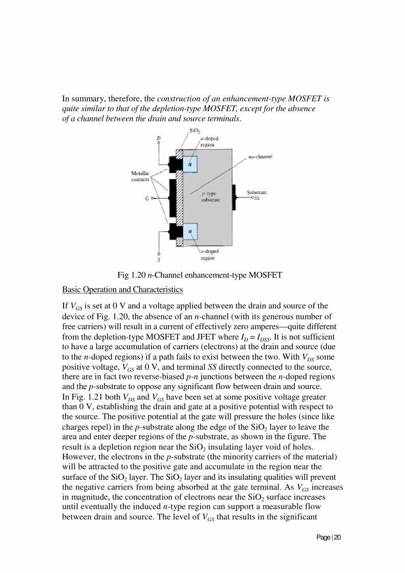
The basic construction of the n-channel enhancement-type MOSFET is
provided in Fig. 1.20. A slab of p-type material is formed from a silicon base
and is again referred to as the substrate. As with the depletion-type MOSFET,
the substrate is sometimes internally connected to the source terminal, while in
other cases a fourth lead is made available for external control of its potential
level. The source and drain terminals are again connected through metallic
contacts to n-doped regions, but note in Fig. 1.20 the absence of a channel
between the two n-doped regions. This is the primary difference between the
construction of depletion-type and enhancement-type MOSFETs—the absence
of a channel as a constructed component of the device. The SiO2 layer is still present to isolate the gate metallic platform from the region between the drain and source, but now it is simply separated from a section of the p-type material.

Anjuman-I-Islam’s Kalsekar Technical Campus, New Panvel
Page | 19
Anjuman-I-Islam’s Kalsekar Technical Campus, New Panvel
In summary, therefore, the construction of an enhancement-type MOSFET is
quite similar to that of the depletion-type MOSFET, except for the absence
of a channel between the drain and source terminals.
Fig 1.20 n-Channel enhancement-type MOSFET
Basic Operation and Characteristics
If VGS is set at 0 V and a voltage applied between the drain and source of the
device of Fig. 1.20, the absence of an n-channel (with its generous number of
free carriers) will result in a current of effectively zero amperes—quite different
from the depletion-type MOSFET and JFET where ID = IDSS. It is not sufficient to have a large accumulation of carriers (electrons) at the drain and source (due
to the n-doped regions) if a path fails to exist between the two. With VDS some
positive voltage, VGS at 0 V, and terminal SS directly connected to the source, there are in fact two reverse-biased p-n junctions between the n-doped regions and the p-substrate to oppose any significant flow between drain and source.
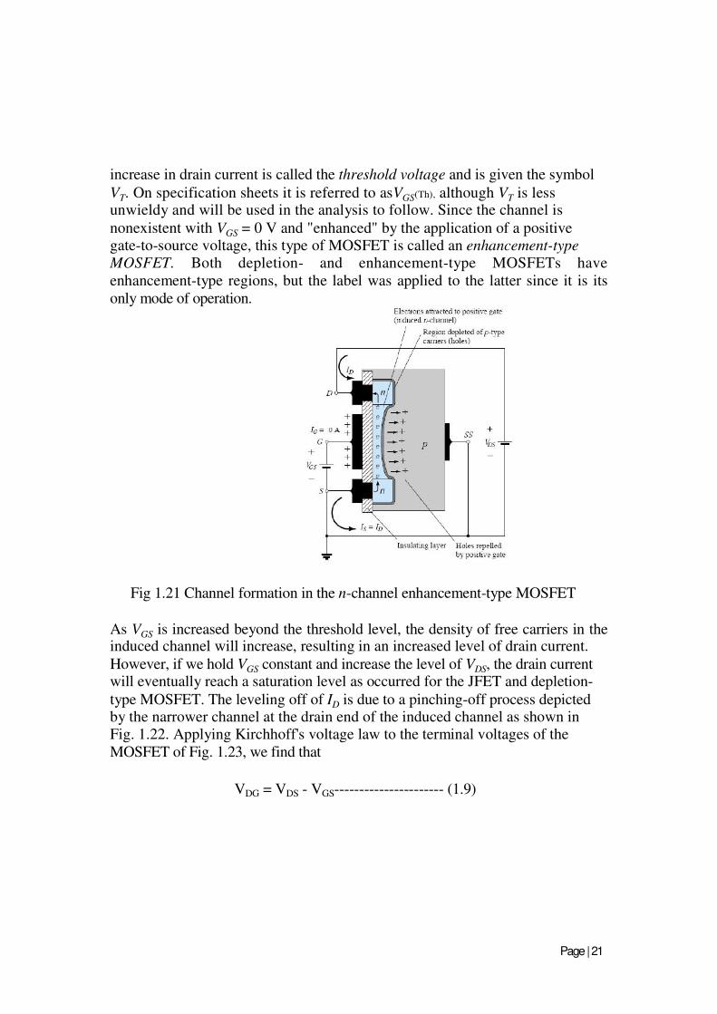
In Fig. 1.21 both VDS and VGS have been set at some positive voltage greater than 0 V, establishing the drain and gate at a positive potential with respect to
the source. The positive potential at the gate will pressure the holes (since like
charges repel) in the p-substrate along the edge of the SiO2 layer to leave the area and enter deeper regions of the p-substrate, as shown in the figure. The
result is a depletion region near the SiO2 insulating layer void of holes. However, the electrons in the p-substrate (the minority carriers of the material) will be attracted to the positive gate and accumulate in the region near the
surface of the SiO2 layer. The SiO2 layer and its insulating qualities will prevent
the negative carriers from being absorbed at the gate terminal. As VGS increases
in magnitude, the concentration of electrons near the SiO2 surface increases until eventually the induced n-type region can support a measurable flow
between drain and source. The level of VGS that results in the significant
Page | 20
Anjuman-I-Islam’s Kalsekar Technical Campus, New Panvel
increase in drain current is called the threshold voltage and is given the symbol
VT. On specification sheets it is referred to asVGS(Th), although VT is less unwieldy and will be used in the analysis to follow. Since the channel is
nonexistent with VGS = 0 V and "enhanced" by the application of a positive gate-to-source voltage, this type of MOSFET is called an enhancement-type
MOSFET. Both depletion- and enhancement-type MOSFETs have
enhancement-type regions, but the label was applied to the latter since it is its
only mode of operation.
Fig 1.21 Channel formation in the n-channel enhancement-type MOSFET
As VGS is increased beyond the threshold level, the density of free carriers in the induced channel will increase, resulting in an increased level of drain current.
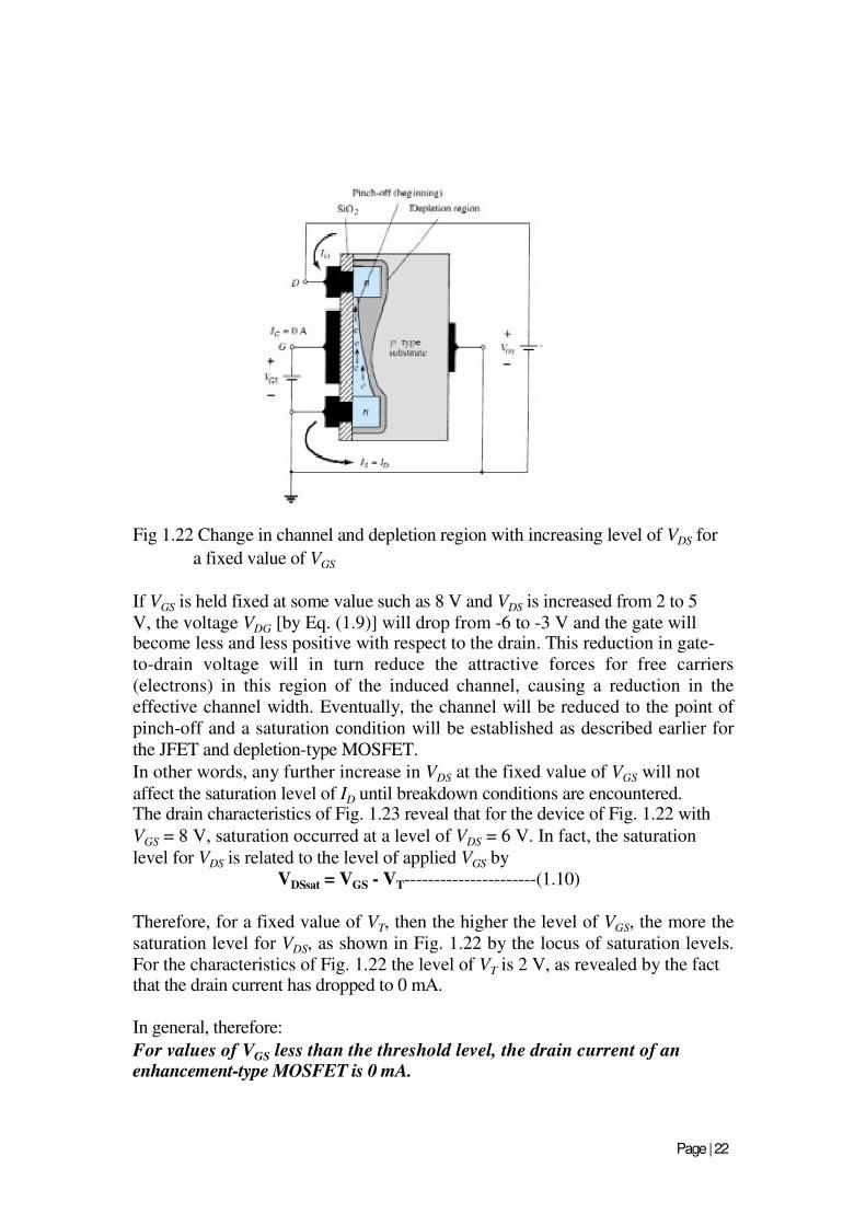
However, if we hold VGS constant and increase the level of VDS, the drain current will eventually reach a saturation level as occurred for the JFET and depletion-
type MOSFET. The leveling off of ID is due to a pinching-off process depicted by the narrower channel at the drain end of the induced channel as shown in Fig. 1.22. Applying Kirchhoff's voltage law to the terminal voltages of the
MOSFET of Fig. 1.23, we find that
VDG = VDS - VGS---------------------- (1.9)
Page | 21
Anjuman-I-Islam’s Kalsekar Technical Campus, New Panvel
Fig 1.22 Change in channel and depletion region with increasing level of VDS for
a fixed value of VGS
If VGS is held fixed at some value such as 8 V and VDS is increased from 2 to 5
V, the voltage VDG [by Eq. (1.9)] will drop from -6 to -3 V and the gate will become less and less positive with respect to the drain. This reduction in gate-
to-drain voltage will in turn reduce the attractive forces for free carriers
(electrons) in this region of the induced channel, causing a reduction in the
effective channel width. Eventually, the channel will be reduced to the point of
pinch-off and a saturation condition will be established as described earlier for
the JFET and depletion-type MOSFET.
In other words, any further increase in VDS at the fixed value of VGS will not
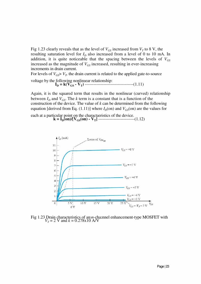
affect the saturation level of ID until breakdown conditions are encountered. The drain characteristics of Fig. 1.23 reveal that for the device of Fig. 1.22 with
VGS = 8 V, saturation occurred at a level of VDS = 6 V. In fact, the saturation
level for VDS is related to the level of applied VGS by
VDSsat = VGS - VT----------------------(1.10)
Therefore, for a fixed value of VT, then the higher the level of VGS, the more the
saturation level for VDS, as shown in Fig. 1.22 by the locus of saturation levels.
For the characteristics of Fig. 1.22 the level of VT is 2 V, as revealed by the fact that the drain current has dropped to 0 mA. In general, therefore:
For values of VGS less than the threshold level, the drain current of an enhancement-type MOSFET is 0 mA.
Page | 22
Anjuman-I-Islam’s Kalsekar Technical Campus, New Panvel
Fig 1.23 clearly reveals that as the level of VGS increased from VT to 8 V, the
resulting saturation level for ID also increased from a level of 0 to 10 mA. In
addition, it is quite noticeable that the spacing between the levels of VGS
increased as the magnitude of VGS increased, resulting in ever-increasing increments in drain current.
For levels of VGS> VT, the drain current is related to the applied gate-to-source
voltage by the following nonlin2ear relationship: ID = k(VGS - VT) ----------------------------------(1.11)
Again, it is the squared term that results in the nonlinear (curved) relationship
between ID and VGS. The k term is a constant that is a function of the construction of the device. The value of k can be determined from the following
equation [derived from Eq. (1.11)] where ID(on) and VGS(on) are the values for
each at a particular point on the charact2eristics of the device. k = ID(on)/[VGS(on) - VT] --------------------------(1.12)
Fig 1.23 Drain characteristics of an3n-cha2nnel enhancement-type MOSFET with VT = 2 V and k = 0.278x10 A/V
Page | 23
Anjuman-I-Islam’s Kalsekar Technical Campus, New Panvel
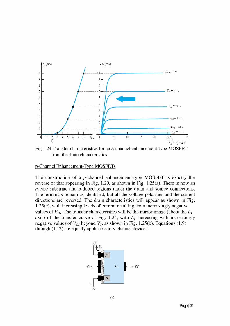
Fig 1.24 Transfer characteristics for an n-channel enhancement-type MOSFET
from the drain characteristics
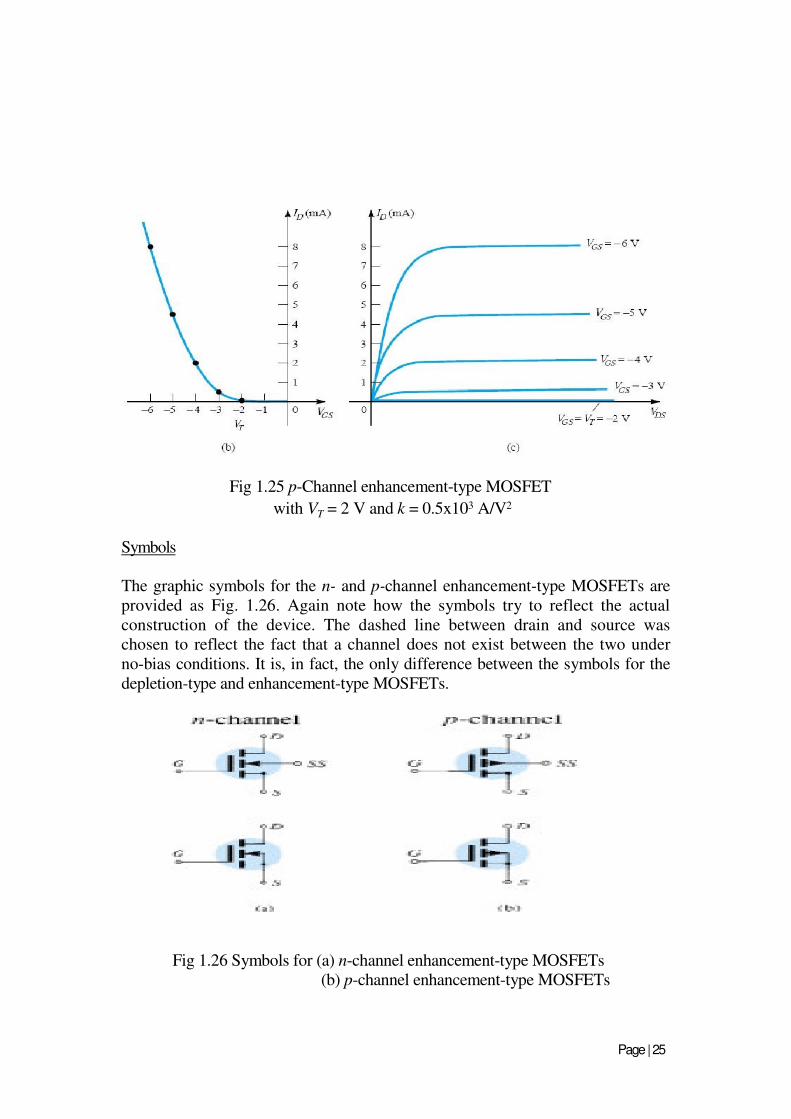
p-Channel Enhancement-Type MOSFETs
The construction of a p-channel enhancement-type MOSFET is exactly the
reverse of that appearing in Fig. 1.20, as shown in Fig. 1.25(a). There is now an
n-type substrate and p-doped regions under the drain and source connections.
The terminals remain as identified, but all the voltage polarities and the current
directions are reversed. The drain characteristics will appear as shown in Fig.
1.25(c), with increasing levels of current resulting from increasingly negative
values of VGS. The transfer characteristics will be the mirror image (about the ID
axis) of the transfer curve of Fig. 1.24, with ID increasing with increasingly
negative values of VGS beyond VT, as shown in Fig. 1.25(b). Equations (1.9) through (1.12) are equally applicable to p-channel devices.
Page | 24
Anjuman-I-Islam’s Kalsekar Technical Campus, New Panvel
Fig 1.25 p-Channel enhancement-type MOSFET
with VT = 2 V and k = 0.5x10³ A/V2
Symbols
The graphic symbols for the n- and p-channel enhancement-type MOSFETs are
provided as Fig. 1.26. Again note how the symbols try to reflect the actual
construction of the device. The dashed line between drain and source was
chosen to reflect the fact that a channel does not exist between the two under
no-bias conditions. It is, in fact, the only difference between the symbols for the
depletion-type and enhancement-type MOSFETs.
Fig 1.26 Symbols for (a) n-channel enhancement-type MOSFETs
(b) p-channel enhancement-type MOSFETs
Page | 25
Anjuman-I-Islam’s Kalsekar Technical Campus, New Panvel
Topic 2 BIASING OF BJT’S
2.1 INTRODUCTION
The analysis or design of a transistor amplifier requires knowledge of both the
dc and ac response of the system. Too often it is assumed that the transistor is a
magical device that can raise the level of the applied ac input without the
assistance of an external energy source. In actuality, the improved output ac
power level is the result of a transfer of energy from the applied dc supplies.
The analysis or design of any electronic amplifier therefore has two
components: the dc portion and the ac portion. Fortunately, the superposition
theorem is applicable and the investigation of the dc conditions can be totally
separated from the ac response. However, one must keep in mind that during the
design or synthesis stage the choice of parameters for the required dc levels will
affect the ac response, and vice versa.
The dc level of operation of a transistor is controlled by a number of factors,
including the range of possible operating points on the device characteristics.
Once the desired dc current and voltage levels have been defined, a network
must be constructed that will establish the desired operating point. Each design
will also determine the stability of the system, that is, how sensitive the system is
to temperature variations.
Basic relationships for a transistor:
VBE = 0.7V------------------------------(2.1)
IE = (1+ ββββ)IB = IC -----------------------(2.2)
IC = ββββIB------------------------------------(2.3)
In most instances the base current IB is the first quantity to be determined. Once IB
is known, the relationships of Eqs. (2.1) through (2.3) can be applied to find the remaining quantities of interest.
2.2 OPERATING POINT
The term biasing appearing in the title of this chapter is an all-inclusive term for
the application of dc voltages to establish a fixed level of current and voltage.
For transistor amplifiers the resulting dc current and voltage establish an
operating point on the characteristics that define the region that will be
employed for amplification of the applied signal. Since the operating point is a
fixed point on the characteristics, it is also called the quiescent point
(abbreviated Q-point). By definition, quiescent means quiet, still, inactive.
Figure 1.1 shows a general output device characteristic with four operating
points indicated. The biasing circuit can be designed to set the device operation at
any of these points or others within the active region. The maximum ratings
are indicated on the characteristics of Fig. 1.1 by a horizontal line for the
maximum collector current ICmax and a vertical line at the maximum collector-
Page | 28
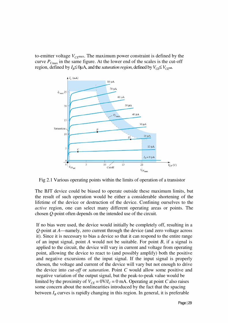
Anjuman-I-Islam’s Kalsekar Technical Campus, New Panvel
to-emitter voltage VCEmax. The maximum power constraint is defined by the
curve PCmax in the same figure. At the lower end of the scales is the cut-off
region, defined by IB≤ 0µA, and the saturation region, defined by VCE≤ VCEsat.
Fig 2.1 Various operating points within the limits of operation of a transistor
The BJT device could be biased to operate outside these maximum limits, but
the result of such operation would be either a considerable shortening of the
lifetime of the device or destruction of the device. Confining ourselves to the
active region, one can select many different operating areas or points. The
chosen Q-point often depends on the intended use of the circuit.
If no bias were used, the device would initially be completely off, resulting in a
Q-point at A—namely, zero current through the device (and zero voltage across
it). Since it is necessary to bias a device so that it can respond to the entire range
of an input signal, point A would not be suitable. For point B, if a signal is
applied to the circuit, the device will vary in current and voltage from operating
point, allowing the device to react to (and possibly amplify) both the positive
and negative excursions of the input signal. If the input signal is properly
chosen, the voltage and current of the device will vary but not enough to drive
the device into cut-off or saturation. Point C would allow some positive and
negative variation of the output signal, but the peak-to-peak value would be
limited by the proximity of VCE = 0V/IC = 0 mA. Operating at point C also raises
some concern about the nonlinearities introduced by the fact that the spacing
between IB curves is rapidly changing in this region. In general, it is preferable
Page | 29
Anjuman-I-Islam’s Kalsekar Technical Campus, New Panvel
to operate where the gain of the device is fairly constant (or linear) to ensure
that the amplification over the entire swing of input signal is the same. Point B
is a region of more linear spacing and therefore more linear operation, as shown
in Fig. 2.1. Point D sets the device operating point near the maximum voltage
and power level. The output voltage swing in the positive direction is thus
limited if the maximum voltage is not to be exceeded. Point B therefore seems
the best operating point in terms of linear gain and largest possible voltage and
current swing. This is usually the desired condition for small-signal amplifiers
but not the case necessarily for power amplifiers.
One other very important biasing factor must be considered. Having selected
and biased the BJT at a desired operating point, the effect of temperature must
also be taken into account. Temperature causes the device parameters such as
the transistor current gain (βac) and the transistor leakage current (ICEO) to change. Higher temperatures result in increased leakage currents in the device, thereby changing the operating condition set by the biasing network. The result
is that the network design must also provide a degree of temperature stability so
that temperature changes result in minimum changes in the operating point. This
maintenance of the operating point can be specified by a stability factor, S,
which indicates the degree of change in operating point due to a temperature
variation. A highly stable circuit is desirable, and the stability of a few basic
bias circuits will be compared.
For the BJT to be biased in its linear or active operating region the following
must be true:
1. The base-emitter junction must be forward-biased (p-region voltage
more positive), with a resulting forward-bias voltage of about 0.6to 0.7 V.
2. The base-collector junction must be reverse-biased (n-region more
positive), with the reverse-bias voltage being any value within the
maximum limits of the device.
[Note that for forward bias the voltage across the p-n junction is p-positive,
while for reverse bias it is opposite (reverse) with n-positive.]
Operation in the cut-off, saturation, and linear regions of the BJT characteristic
are provided as follows:
1. Linear-region operation:
Base-emitter junction forward biased Base-
collector junction reverse biased
2. Cut-off-region operation:
Base-emitter junction reverse biased
Page | 30
Anjuman-I-Islam’s Kalsekar Technical Campus, New Panvel
3. Saturation-region operation:
Base-emitter junction forward biased
Base-collector junction forward biased
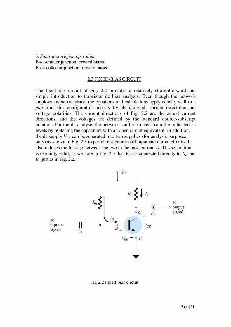
2.3 FIXED-BIAS CIRCUIT
The fixed-bias circuit of Fig. 2.2 provides a relatively straightforward and
simple introduction to transistor dc bias analysis. Even though the network
employs annpn transistor, the equations and calculations apply equally well to a
pnp transistor configuration merely by changing all current directions and
voltage polarities. The current directions of Fig. 2.2 are the actual current
directions, and the voltages are defined by the standard double-subscript
notation. For the dc analysis the network can be isolated from the indicated ac
levels by replacing the capacitors with an open circuit equivalent. In addition,
the dc supply VCC can be separated into two supplies (for analysis purposes only) as shown in Fig. 2.3 to permit a separation of input and output circuits. It
also reduces the linkage between the two to the base current IB. The separation
is certainly valid, as we note in Fig. 2.3 that VCC is connected directly to RB and
RC just as in Fig. 2.2.
Fig 2.2 Fixed-bias circuit
Page | 31
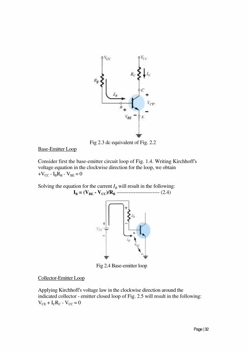
Anjuman-I-Islam’s Kalsekar Technical Campus, New Panvel
Fig 2.3 dc equivalent of Fig. 2.2
Base-Emitter Loop
Consider first the base-emitter circuit loop of Fig. 1.4. Writing Kirchhoff's
voltage equation in the clockwise direction for the loop, we obtain
+VCC - IBRB - VBE = 0
Solving the equation for the current IB will result in the following:
IB = (VBE - VCC)/RB ------------------------- (2.4)
Fig 2.4 Base-emitter loop
Collector-Emitter Loop
Applying Kirchhoff's voltage law in the clockwise direction around the
indicated collector - emitter closed loop of Fig. 2.5 will result in the following:
VCE + ICRC - VCC = 0
Page | 32
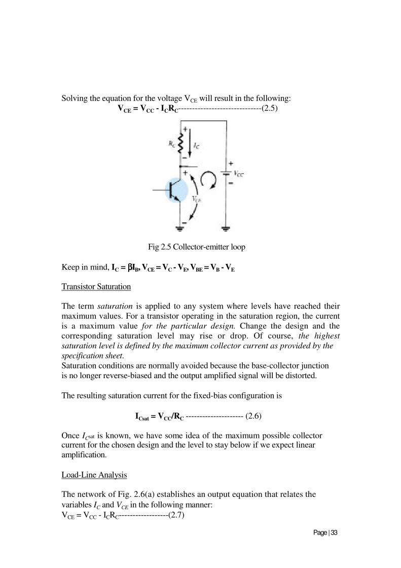
Anjuman-I-Islam’s Kalsekar Technical Campus, New Panvel
Solving the equation for the voltage VCE will result in the following:
VCE = VCC - ICRC------------------------------(2.5)
Fig 2.5 Collector-emitter loop
Keep in mind, IC = ββββIB, VCE = VC - VE, VBE = VB - VE
Transistor Saturation
The term saturation is applied to any system where levels have reached their
maximum values. For a transistor operating in the saturation region, the current
is a maximum value for the particular design. Change the design and the
corresponding saturation level may rise or drop. Of course, the highest
saturation level is defined by the maximum collector current as provided by the
specification sheet.
Saturation conditions are normally avoided because the base-collector junction
is no longer reverse-biased and the output amplified signal will be distorted.
The resulting saturation current for the fixed-bias configuration is
ICsat = VCC/RC --------------------- (2.6)
Once ICsat is known, we have some idea of the maximum possible collector current for the chosen design and the level to stay below if we expect linear
amplification.
Load-Line Analysis
The network of Fig. 2.6(a) establishes an output equation that relates the
variables IC and VCE in the following manner:
VCE = VCC - ICRC------------------(2.7)
Page | 33
Anjuman-I-Islam’s Kalsekar Technical Campus, New Panvel
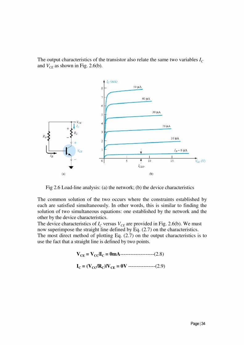
The output characteristics of the transistor also relate the same two variables IC
and VCE as shown in Fig. 2.6(b).
Fig 2.6 Load-line analysis: (a) the network; (b) the device characteristics
The common solution of the two occurs where the constraints established by
each are satisfied simultaneously. In other words, this is similar to finding the
solution of two simultaneous equations: one established by the network and the
other by the device characteristics.
The device characteristics of IC versus VCE are provided in Fig. 2.6(b). We must now superimpose the straight line defined by Eq. (2.7) on the characteristics.
The most direct method of plotting Eq. (2.7) on the output characteristics is to
use the fact that a straight line is defined by two points.
VCE = VCC|IC = 0mA--------------------(2.8)
IC = (VCC/RC)|VCE = 0V ----------------(2.9)
Page | 34
Anjuman-I-Islam’s Kalsekar Technical Campus, New Panvel
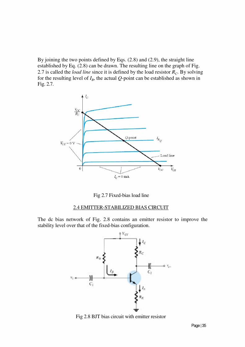
By joining the two points defined by Eqs. (2.8) and (2.9), the straight line
established by Eq. (2.8) can be drawn. The resulting line on the graph of Fig.
2.7 is called the load line since it is defined by the load resistor RC. By solving
for the resulting level of IB, the actual Q-point can be established as shown in Fig. 2.7.
Fig 2.7 Fixed-bias load line
2.4 EMITTER-STABILIZED BIAS CIRCUIT
The dc bias network of Fig. 2.8 contains an emitter resistor to improve the
stability level over that of the fixed-bias configuration.
Fig 2.8 BJT bias circuit with emitter resistor
Page | 35
Anjuman-I-Islam’s Kalsekar Technical Campus, New Panvel
Base-Emitter Loop
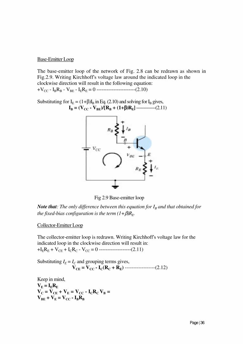
The base-emitter loop of the network of Fig. 2.8 can be redrawn as shown in
Fig.2.9. Writing Kirchhoff's voltage law around the indicated loop in the
clockwise direction will result in the following equation:
+VCC - IBRB - VBE - IERE = 0 -----------------------(2.10) Substituting for IE = (1+β)IB in Eq. (2.10) and solving for IB gives,
IB = (VCC - VBE)/[RB + (1+ββββ)RE] -------------(2.11)
Fig 2.9 Base-emitter loop
Note that: The only difference between this equation for IB and that obtained for
the fixed-bias configuration is the term (1+β)RE.
Collector-Emitter Loop
The collector-emitter loop is redrawn. Writing Kirchhoff's voltage law for the
indicated loop in the clockwise direction will result in:
+IERE + VCE + ICRC - VCC = 0 -------------------(2.11)
Substituting IE = IC and grouping terms gives,
VCE = VCC - IC(RC + RE) ------------------(2.12)
Keep in mind,
VE = IERE
VC = VCE + VE = VCC - ICRC VB =
VBE + VE = VCC - IBRB
Page | 36
Anjuman-I-Islam’s Kalsekar Technical Campus, New Panvel
Improved Bias Stability
The addition of the emitter resistor to the dc bias of the BJT provides improved
stability, that is, the dc bias currents and voltages remain closer to where they
were set by the circuit when outside conditions, such as temperature, and
transistor beta, change.
Saturation Level The collector saturation level or maximum collector current for an emitter-bias
design can be determined using the same approach applied to the fixed-bias
configuration:
ICsat = VCC/(RC + RE)-------------------------(2.13)
The addition of the emitter resistor reduces the collector saturation level below
that obtained with a fixed-bias configuration using the same collector resistor.
Load-Line Analysis
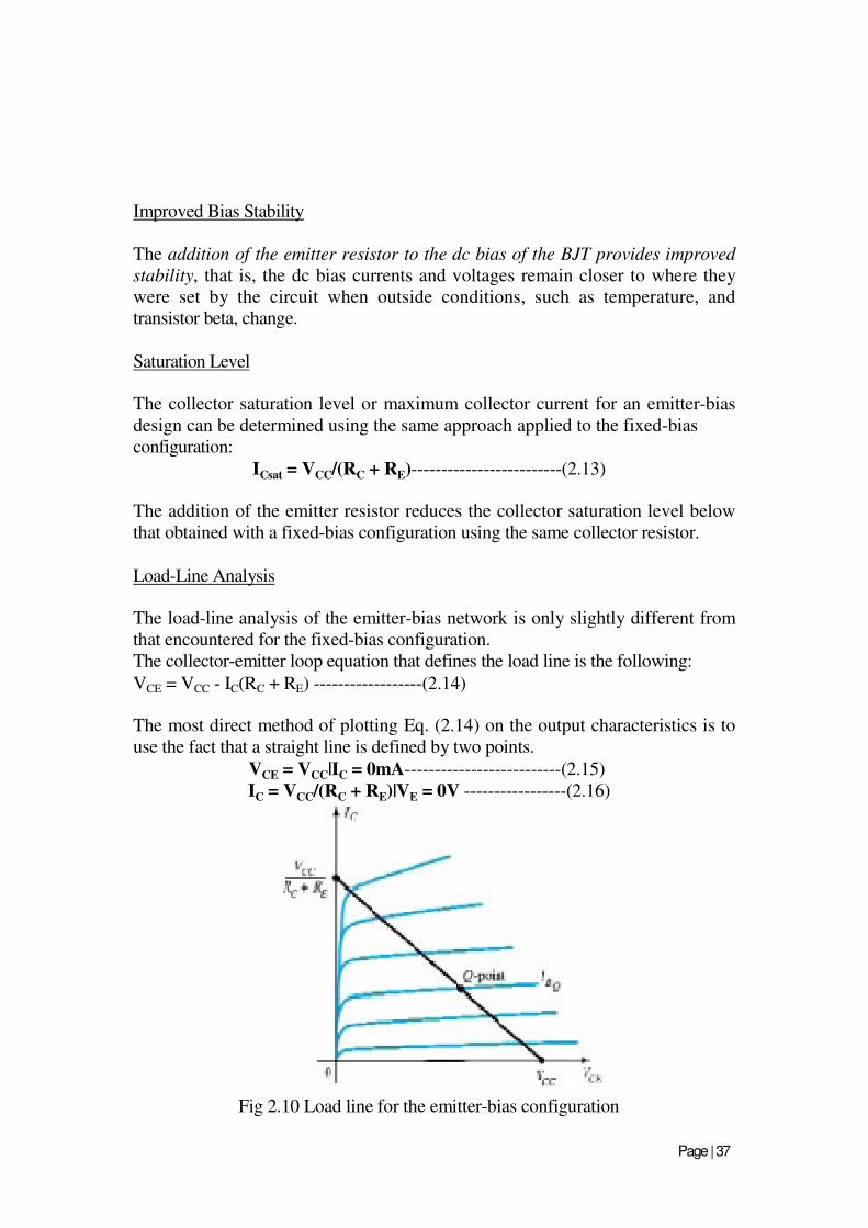
The load-line analysis of the emitter-bias network is only slightly different from
that encountered for the fixed-bias configuration.
The collector-emitter loop equation that defines the load line is the following:
VCE = VCC - IC(RC + RE) ------------------(2.14) The most direct method of plotting Eq. (2.14) on the output characteristics is to
use the fact that a straight line is defined by two points.
VCE = VCC|IC = 0mA--------------------------(2.15)
IC = VCC/(RC + RE)|VE = 0V -----------------(2.16)
Fig 2.10 Load line for the emitter-bias configuration
Page | 37
Anjuman-I-Islam’s Kalsekar Technical Campus, New Panvel
2.5 VOLTAGE-DIVIDER BIAS
In the previous bias configurations the bias current ICQ and voltage VCEQ were a
function of the current gain (β) of the transistor. However, since β is temperature sensitive, especially for silicon transistors, and the actual value of
beta is usually not well defined, it would be desirable to develop a bias circuit
that is less dependent, or in fact, independent of the transistor beta. The voltage-
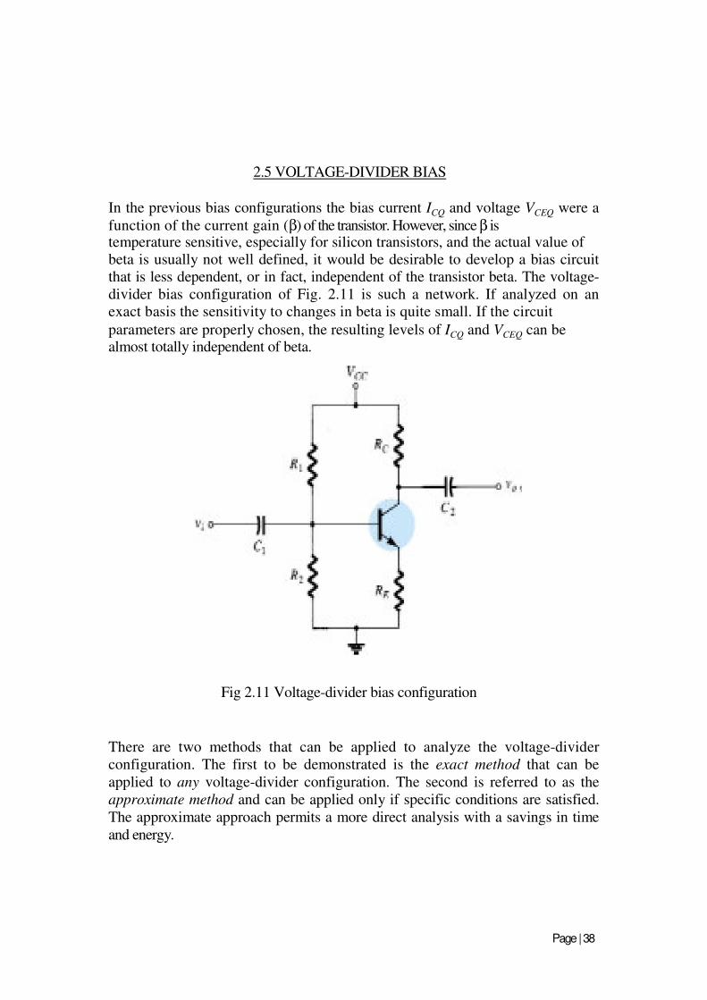
divider bias configuration of Fig. 2.11 is such a network. If analyzed on an
exact basis the sensitivity to changes in beta is quite small. If the circuit
parameters are properly chosen, the resulting levels of ICQ and VCEQ can be almost totally independent of beta.
Fig 2.11 Voltage-divider bias configuration
There are two methods that can be applied to analyze the voltage-divider
configuration. The first to be demonstrated is the exact method that can be
applied to any voltage-divider configuration. The second is referred to as the
approximate method and can be applied only if specific conditions are satisfied.
The approximate approach permits a more direct analysis with a savings in time
and energy.
Page | 38
Anjuman-I-Islam’s Kalsekar Technical Campus, New Panvel
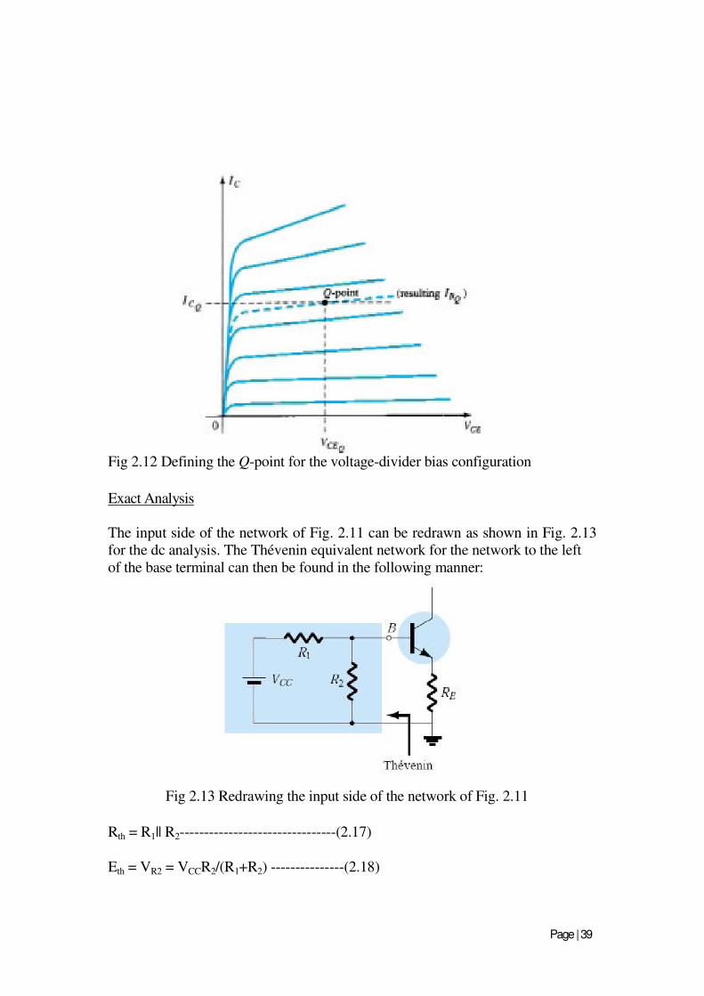
Fig 2.12 Defining the Q-point for the voltage-divider bias configuration
Exact Analysis
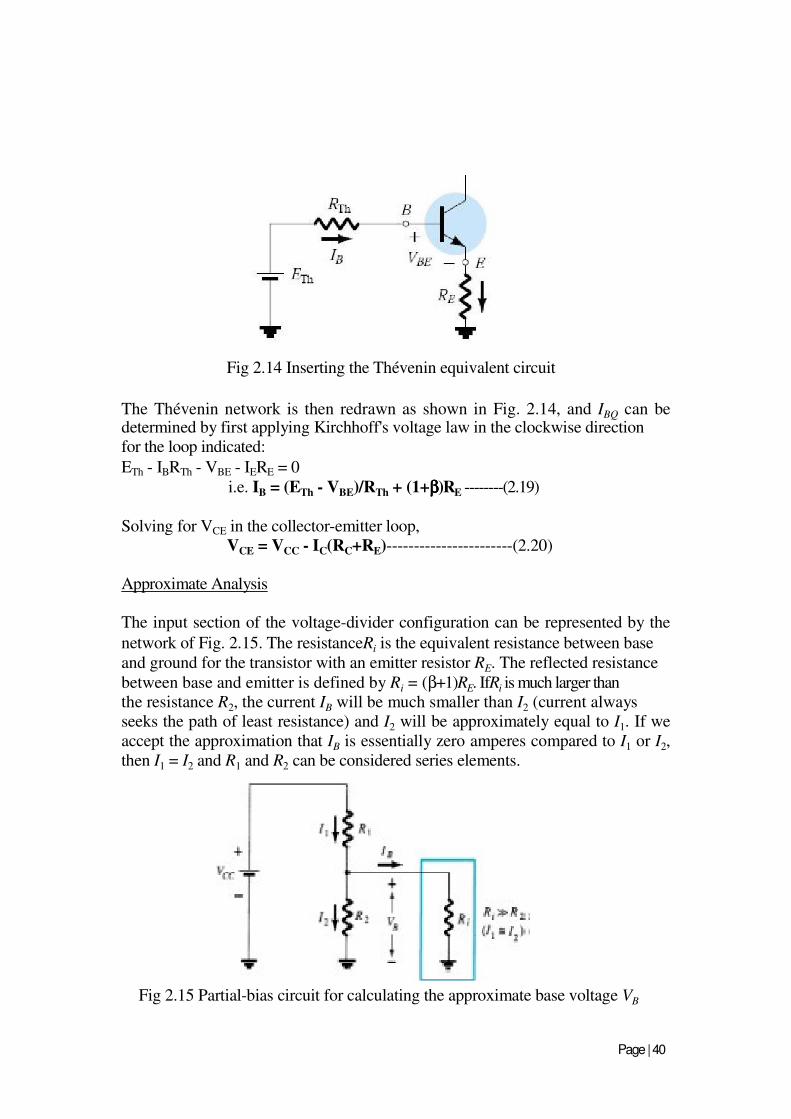
The input side of the network of Fig. 2.11 can be redrawn as shown in Fig. 2.13
for the dc analysis. The Thévenin equivalent network for the network to the left
of the base terminal can then be found in the following manner:
Fig 2.13 Redrawing the input side of the network of Fig. 2.11
Rth = R1|| R2--------------------------------(2.17)
Eth = VR2 = VCCR2/(R1+R2) ---------------(2.18)
Page | 39
Anjuman-I-Islam’s Kalsekar Technical Campus, New Panvel
Fig 2.14 Inserting the Thévenin equivalent circuit
The Thévenin network is then redrawn as shown in Fig. 2.14, and IBQ can be determined by first applying Kirchhoff's voltage law in the clockwise direction
for the loop indicated:
ETh - IBRTh - VBE - IERE = 0
i.e. IB = (ETh - VBE)/RTh + (1+ββββ)RE --------(2.19)
Solving for VCE in the collector-emitter loop,
VCE = VCC - IC(RC+RE)-----------------------(2.20)
Approximate Analysis
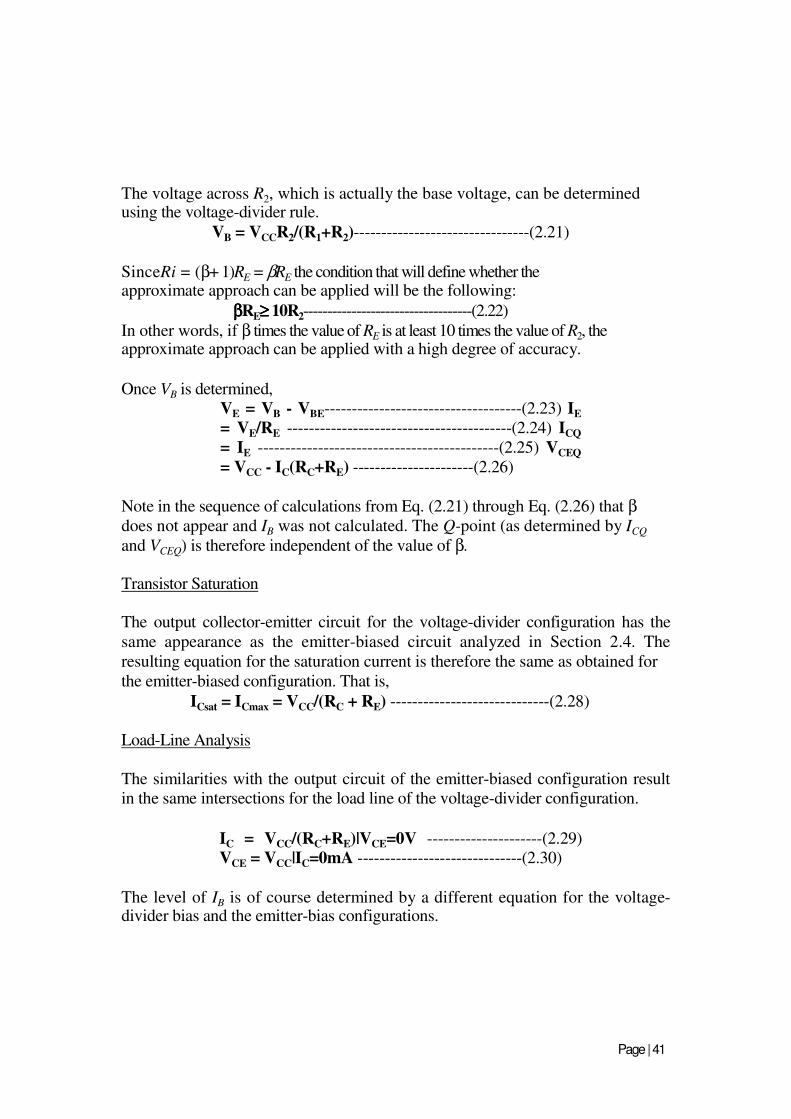
The input section of the voltage-divider configuration can be represented by the
network of Fig. 2.15. The resistanceRi is the equivalent resistance between base
and ground for the transistor with an emitter resistor RE. The reflected resistance
between base and emitter is defined by Ri = (β+1)RE. IfRi is much larger than
the resistance R2, the current IB will be much smaller than I2 (current always
seeks the path of least resistance) and I2 will be approximately equal to I1. If we
accept the approximation that IB is essentially zero amperes compared to I1 or I2,
then I1 = I2 and R1 and R2 can be considered series elements.
Fig 2.15 Partial-bias circuit for calculating the approximate base voltage VB
Page | 40
Anjuman-I-Islam’s Kalsekar Technical Campus, New Panvel
The voltage across R2, which is actually the base voltage, can be determined using the voltage-divider rule.
VB = VCCR2/(R1+R2)--------------------------------(2.21)
SinceRi = (β+ 1)RE = βRE the condition that will define whether the approximate approach can be applied will be the following:
ββββRE≥≥≥≥ 10R2-----------------------------------(2.22)
In other words, if β times the value of RE is at least 10 times the value of R2, the approximate approach can be applied with a high degree of accuracy.
Once VB is determined,
VE = VB - VBE------------------------------------(2.23) IE
= VE/RE -----------------------------------------(2.24) ICQ
= IE --------------------------------------------(2.25) VCEQ
= VCC - IC(RC+RE) ----------------------(2.26)
Note in the sequence of calculations from Eq. (2.21) through Eq. (2.26) that β
does not appear and IB was not calculated. The Q-point (as determined by ICQ
and VCEQ) is therefore independent of the value of β.
Transistor Saturation
The output collector-emitter circuit for the voltage-divider configuration has the
same appearance as the emitter-biased circuit analyzed in Section 2.4. The
resulting equation for the saturation current is therefore the same as obtained for
the emitter-biased configuration. That is,
ICsat = ICmax = VCC/(RC + RE) -----------------------------(2.28)
Load-Line Analysis
The similarities with the output circuit of the emitter-biased configuration result
in the same intersections for the load line of the voltage-divider configuration.
IC = VCC/(RC+RE)|VCE=0V ---------------------(2.29)
VCE = VCC|IC=0mA ------------------------------(2.30)
The level of IB is of course determined by a different equation for the voltage- divider bias and the emitter-bias configurations.
Page | 41
Anjuman-I-Islam’s Kalsekar Technical Campus, New Panvel
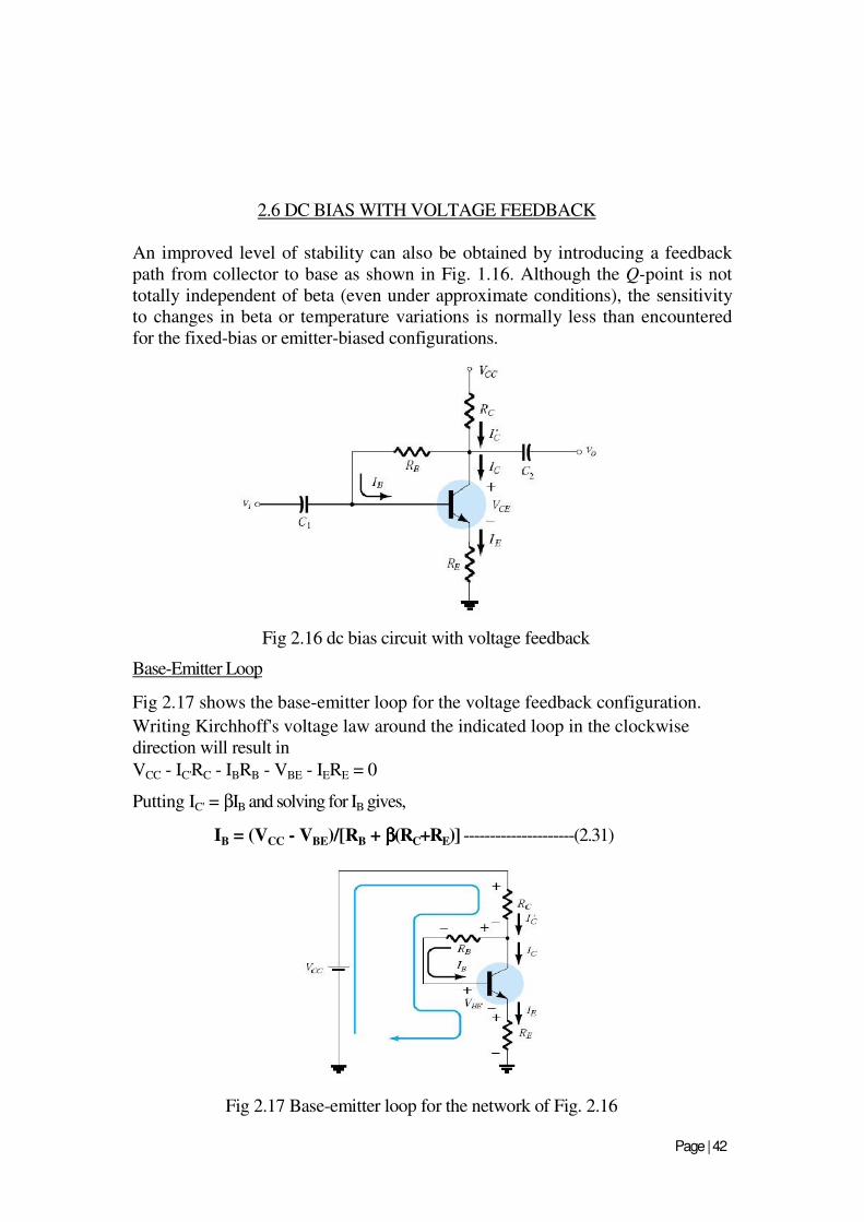
2.6 DC BIAS WITH VOLTAGE FEEDBACK
An improved level of stability can also be obtained by introducing a feedback
path from collector to base as shown in Fig. 1.16. Although the Q-point is not
totally independent of beta (even under approximate conditions), the sensitivity
to changes in beta or temperature variations is normally less than encountered
for the fixed-bias or emitter-biased configurations.
Fig 2.16 dc bias circuit with voltage feedback
Base-Emitter Loop
Fig 2.17 shows the base-emitter loop for the voltage feedback configuration.
Writing Kirchhoff's voltage law around the indicated loop in the clockwise
direction will result in
VCC - IC'RC - IBRB - VBE - IERE = 0
Putting IC' = βIB and solving for IB gives,
IB = (VCC - VBE)/[RB + ββββ(RC+RE)] ---------------------(2.31)
Fig 2.17 Base-emitter loop for the network of Fig. 2.16
Page | 42
Anjuman-I-Islam’s Kalsekar Technical Campus, New Panvel
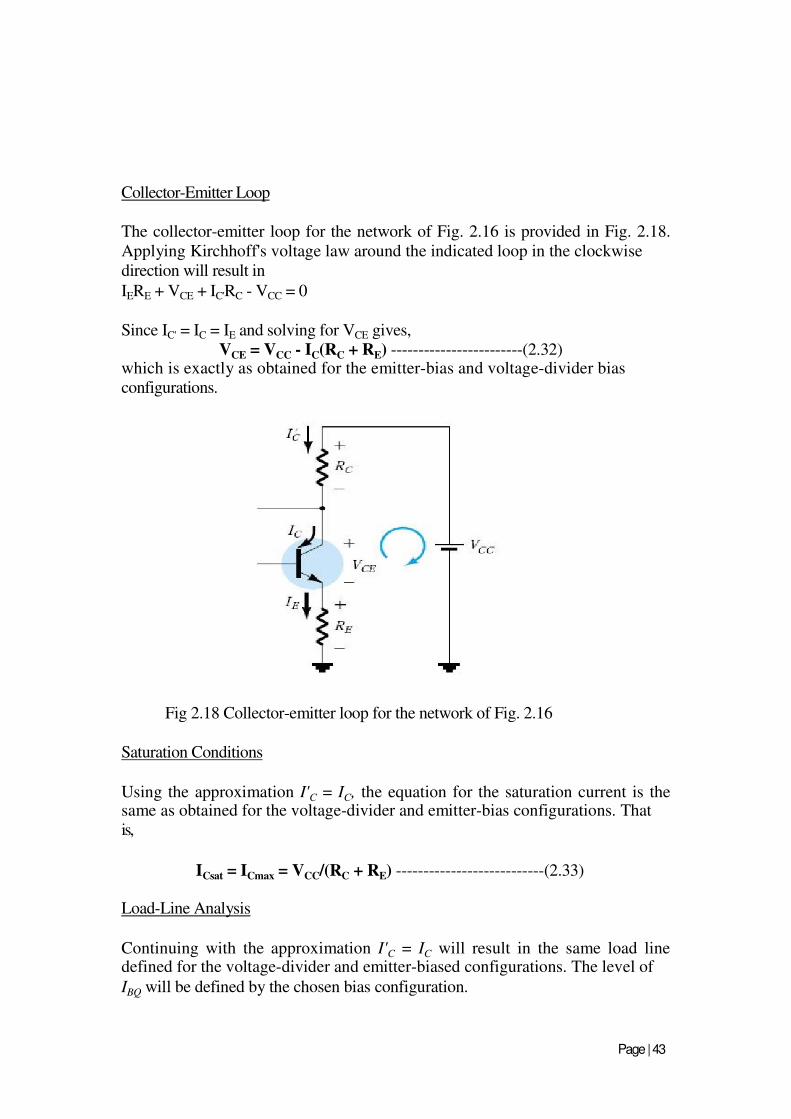
Collector-Emitter Loop
The collector-emitter loop for the network of Fig. 2.16 is provided in Fig. 2.18.
Applying Kirchhoff's voltage law around the indicated loop in the clockwise
direction will result in
IERE + VCE + IC'RC - VCC = 0
Since IC' = IC = IE and solving for VCE gives,
VCE = VCC - IC(RC + RE) ------------------------(2.32) which is exactly as obtained for the emitter-bias and voltage-divider bias
configurations.
Fig 2.18 Collector-emitter loop for the network of Fig. 2.16
Saturation Conditions
Using the approximation I'C = IC, the equation for the saturation current is the same as obtained for the voltage-divider and emitter-bias configurations. That
is,
ICsat = ICmax = VCC/(RC + RE) ---------------------------(2.33)
Load-Line Analysis
Continuing with the approximation I'C = IC will result in the same load line defined for the voltage-divider and emitter-biased configurations. The level of
IBQ will be defined by the chosen bias configuration.
Page | 43
Anjuman-I-Islam’s Kalsekar Technical Campus, New Panvel
2.7 BIAS STABILIZATION
The stability of a system is a measure of the sensitivity of a network to
variations in its parameters. In any amplifier employing a transistor the collector
current IC is sensitive to each of the following parameters: ββββ: increases with increase in temperature |VBE|: decreases about 7.5 mV per degree Celsius (°C) increase in temperature
ICO (reverse saturation current): doubles in value for every 10°C increase in Temperature
Stability Factors,S(ICO), S(VBE), and S(β) A stability factor, S, is defined for each of the parameters affecting bias stability
as listed below:
S(ICO) = ∆IC/∆ICO --------------------------(2.34) S(VBE) = ∆IC/∆VBE ------------------------(2.35) S(ββββ) = ∆IC/ββββ ---------------------------------(2.36) In each case, the delta symbol (∆) signifies change in that quantity. The numerator of each equation is the change in collector current as established by the change in the quantity in the denominator. For a particular configuration, if
a change in ICO fails to produce a significant change in IC, the stability factor
defined by S(ICO) = ∆IC/∆ICO will be quite small. In other words: Networks that are quite stable and relatively insensitive to temperature variations have low stability factors.
The higher the stability factor, the more sensitive the network to variations in
that parameter.
S(ICO): EMITTER-BIAS CONFIGURATION
For the emitter-bias configuration, an analysis of the network will result in
S(ICO) = (1+ββββ)[(1+ RB/RE) / (ββββ+1) + RB/RE] ----------------(2.37)
For RB/RE>> (β+1), Eq. (1.37) will reduce to the following:
S(ICO) = (1+ββββ) ------------------------------(2.38) For RB/RE<<1,
S(ICO) = 1 --------------------------------(2.39)
For the range where RB/RE ranges between 1 and (β+1),
S(ICO) = RB/RE -----------------------------(2.40)
Page | 44
Anjuman-I-Islam’s Kalsekar Technical Campus, New Panvel
The results reveal that the emitter-bias configuration is quite stable when the
ratio RB/RE is as small as possible and the least stable when the same ratio
approaches (β+1).
Fixed-Bias Configuration
S(ICO) = (ββββ+1) -------------------------------------------------------------(2.41) The result is a configuration with a poor stability factor and a high sensitivity
to variations in ICO.
Voltage-Divider Bias Configuration
S(ICO) = (1+ββββ)[(1+ RTh/RE) / (ββββ+1) + RTh/RE] -------------------(2.42)
Feedback-Bias Configuration
S(ICO) = (1+ββββ)[(1+ RB/RC) / (ββββ+1) + RB/RC] -------------------------(2.43)
S(VBE): EMITTER-BIAS CONFIGURATION
S(VBE) = -ββββ/[RB + (1+ββββ)RE] = -(ββββ/RE)/[(RB/RE) + (1+ββββ)] ---------------(2.44) Fixed-Bias Configuration (RE = 0Ω)
S(VBE) = -ββββ/RB ------------------------------------(2.45)
For (1+β) >> RB/RE, S(VBE) = -1/RE -------------------------------------(2.46)
revealing that the larger the resistance RE, the lower the stability factor and the more stable the system.
S(β): EMITTER-BIAS CONFIGURATION
S(ββββ) = [IC1(1+RB/RE) / ββββ
1(1+ββββ
2+RB/RE)] --------------(2.46)
The notation IC1
and β1 is used to define their values under one set of network
conditions, while the notation β2 is used to define the new value of beta as
established by such causes as temperature change, variation in β for the same transistor, or a change in transistors.
Page | 45
Anjuman-I-Islam’s Kalsekar Technical Campus, New Panvel
Fixed-Bias Configuration(RE = 0Ω)
S(ββββ) = [IC1(RB + RC) / ββββ
1RB +
RC (1+ββββ2)] ------------------------(2.47)
Summary
Now that the three stability factors of importance have been introduced, the total
effect on the collector current can be determined using the following
equation:
∆IC = S(ICO)∆ICO + S(VBE)∆VBE + S(ββββ)∆ββββ --------------------------(2.48)
The equation may initially appear quite complex, but take note that each
component is simply a stability factor for the configuration multiplied by the
resulting change in a parameter between the temperature limits of interest. In
addition, the ∆IC to be determined is simply the change in IC from the level at room temperature.
For instance, if we examine the fixed-bias configuration, Eq. (2.48) becomes the
following:
∆IC = (β+1)∆ICO + (-β/RB)∆VBE + (IC1/β1)∆β
The effect ofS(ICO) in the design process is becoming a lesser concern because
of improved manufacturing techniques that continue to lower the level of ICO =
ICBO. It should also be mentioned that for a particular transistor the variation in
levels of ICBO and VBE from one transistor to another in a lot is almost negligible compared to the variation in beta. In addition, the results of the analysis above
support the fact that for a good stabilized design:
The ratio RB/RE or RTh/RE should be as small as possible with due consideration to all aspects of the design, including the ac response.
Page | 46
Anjuman-I-Islam’s Kalsekar Technical Campus, New Panvel
Topic 3 BIASING OF FETS AND MOSFETS
3.1 INTRODUCTION
For the field-effect transistor (FET), the relationship between input and output
quantities is nonlinear due to the squared term in Shockley's equation. Linear
relationships result in straight lines when plotted on a graph of one variable
versus the other, while non-linear functions result in curves as obtained for the
transfer characteristics of a JFET. The non-linear relationship between ID and
VGS can complicate the mathematical approach to the dc analysis of FET configurations. A graphical approach may limit solutions to tenths-place
accuracy, but it is a quicker method for most FET amplifiers.
Whereas in bipolar junction transistor (BJT), the biasing level can be obtained
using the characteristic equations VBE = 0.7V, IC = βIB, and IC = IE. The linkage
between input and output variables is provided by β, which is assumed to be fixed in magnitude for the analysis to be performed. The fact that beta is a
constant establishes a linear relationship between IC and IB. Doubling the value
of IB will double the level of IC, and so on. Another distinct difference between the analysis of BJT and FET transistors is
that the input controlling variable for a BJT transistor is a current level, while
for the FET a voltage is the controlling variable. In both cases, however, the
controlled variable on the output side is a current level that also defines the
important voltage levels of the output circuit.
The general relationships that can be applied to the dc analysis of all FET
amplifiers are:
IG = 0A------------------------------(3.1)
ID = IS-------------------------------(3.2)
For JFETS and depletion-type MOSFETs, Shockley's equation is applied to
relate the input and output quantities:
ID = IDSS(1-VGS/VP)2 --------------(3.3)
For enhancement-type MOSFETs, the following equation is applicable:
ID = k(VGS - VT)2 -----------------(3.4)
Page | 47
Anjuman-I-Islam’s Kalsekar Technical Campus, New Panvel
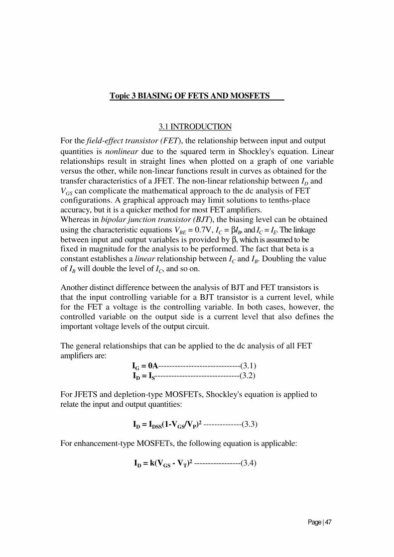
3.2 FIXED-BIAS CONFIGURATION
The simplest of biasing arrangements for the n-channel JFET appears in Fig.
3.1. The fixed-bias configuration is one of the few FET configurations that can
be solved just as directly using either a mathematical or graphical approach.
The configuration of Fig. 3.1 includes the ac levelsVi and Vo and the coupling
capacitors (C1 and C2). The coupling capacitors are "open circuits" for the dc analysis and low impedances (essentially short circuits) for the ac analysis. The
resistor RG is present to ensure that Vi appears at the input to the FET amplifier for the ac analysis.
For the dc analysis,
IG = 0A and VRG = IGRG = (0A)RG = 0V
The zero-volt drop across RG permits replacing RG by a short-circuit equivalent, as appearing in the network of Fig. 3.2 specifically redrawn for the dc analysis. Fig 3.1 Fixed-bias configuration Fig 3.2 Network for dc analysis The fact that the negative terminal of the battery is connected directly to the
defined positive potential of VGS clearly reveals that the polarity of VGS is
directly opposite to that of VGG. Applying Kirchhoff's voltage law in the clockwise direction of the indicated loop of Fig. 3.2 will result in:
VGS = -VGG---------------------------------(3.5)
Since VGG is a fixed dc supply, the voltage VGS is fixed in magnitude, resulting in the notation "fixed-bias configuration."
Page | 48
Anjuman-I-Islam’s Kalsekar Technical Campus, New Panvel
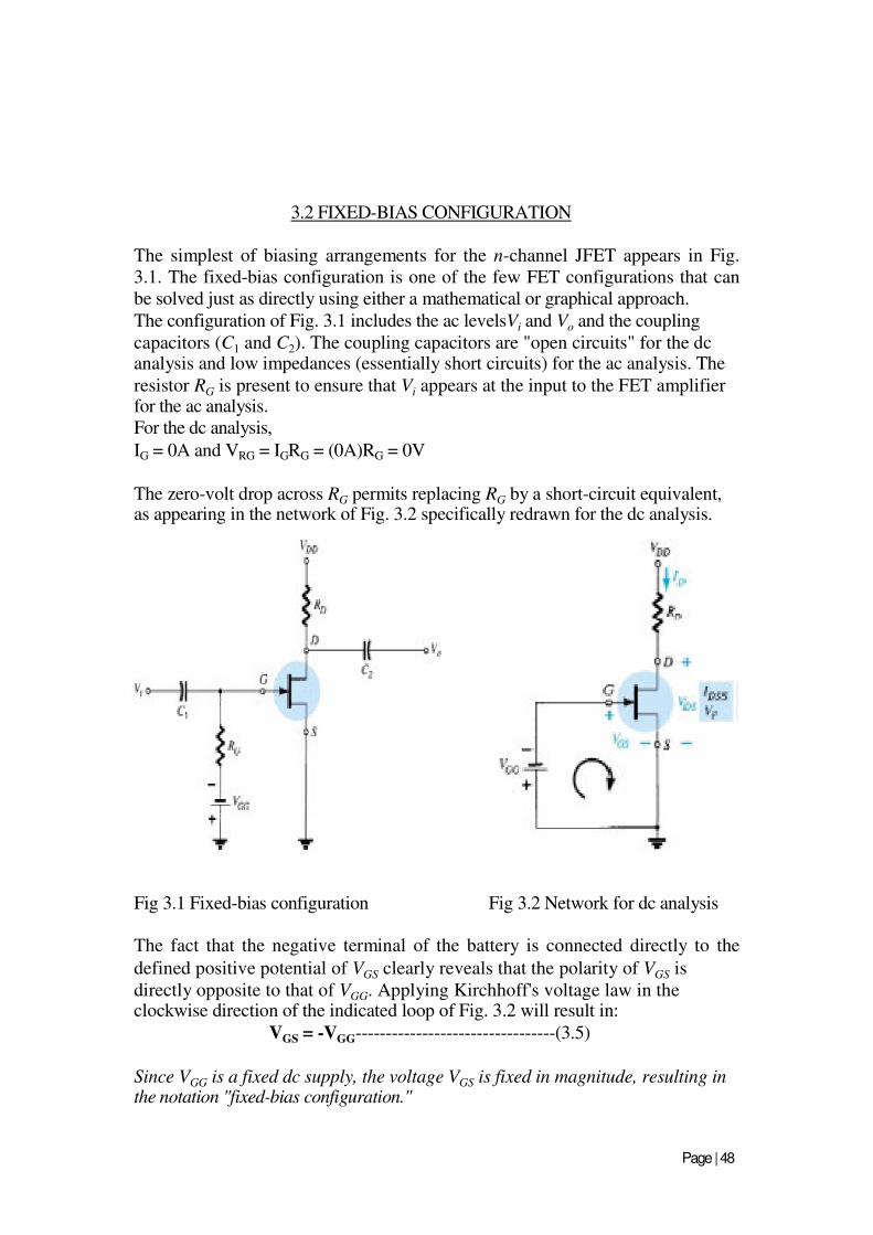
The resulting level of drain current ID is now controlled by Shockley's equation:
ID = IDSS(1-VGS/VP)2
Since VGS is a fixed quantity for this configuration, its magnitude and sign can
simply be substituted into Shockley's equation and the resulting level of ID
calculated. A graphical analysis would require a plot of Shockley's equation as shown in
Fig. 3.3. Choosing VGS= VP/2 will result in a drain current of IDSS/4 when plotting the equation. For the analysis of this chapter, the three points defined
by IDSS, VP, and the intersection just described will be sufficient for plotting the curve.
Fig 3.3 Plotting Shockley's equation
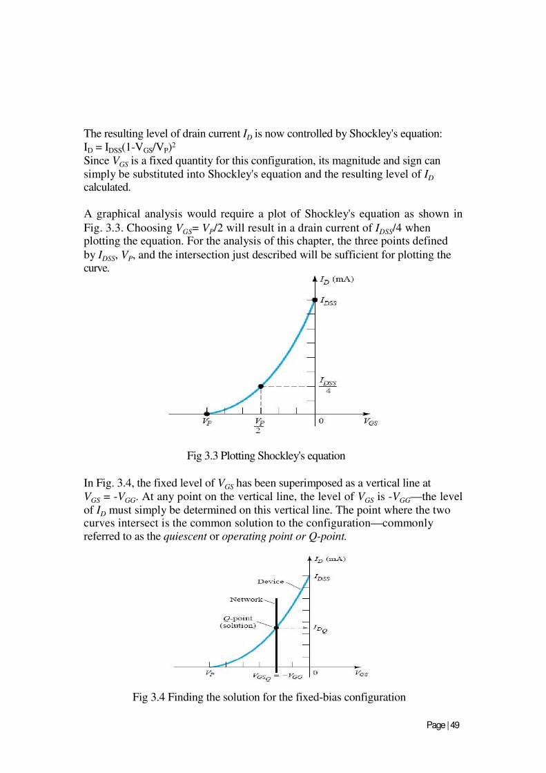
In Fig. 3.4, the fixed level of VGS has been superimposed as a vertical line at
VGS = -VGG. At any point on the vertical line, the level of VGS is -VGG—the level
of ID must simply be determined on this vertical line. The point where the two curves intersect is the common solution to the configuration—commonly referred to as the quiescent or operating point or Q-point.
Fig 3.4 Finding the solution for the fixed-bias configuration
Page | 49
Anjuman-I-Islam’s Kalsekar Technical Campus, New Panvel
The drain-to-source voltage of the output section can be determined by applying
Kirchhoff's voltage law as follows:
+VDS + IDRD - VDD = 0
Or, VDS = VDD - IDRD----------------------------(3.6)
Keep in mind, VS = 0V------------------------------(3.7)
VD = VDS-----------------------------(3.8) VG
= VGS -----------------------------(3.9)
Since the configuration requires two dc supplies, its use is limited.
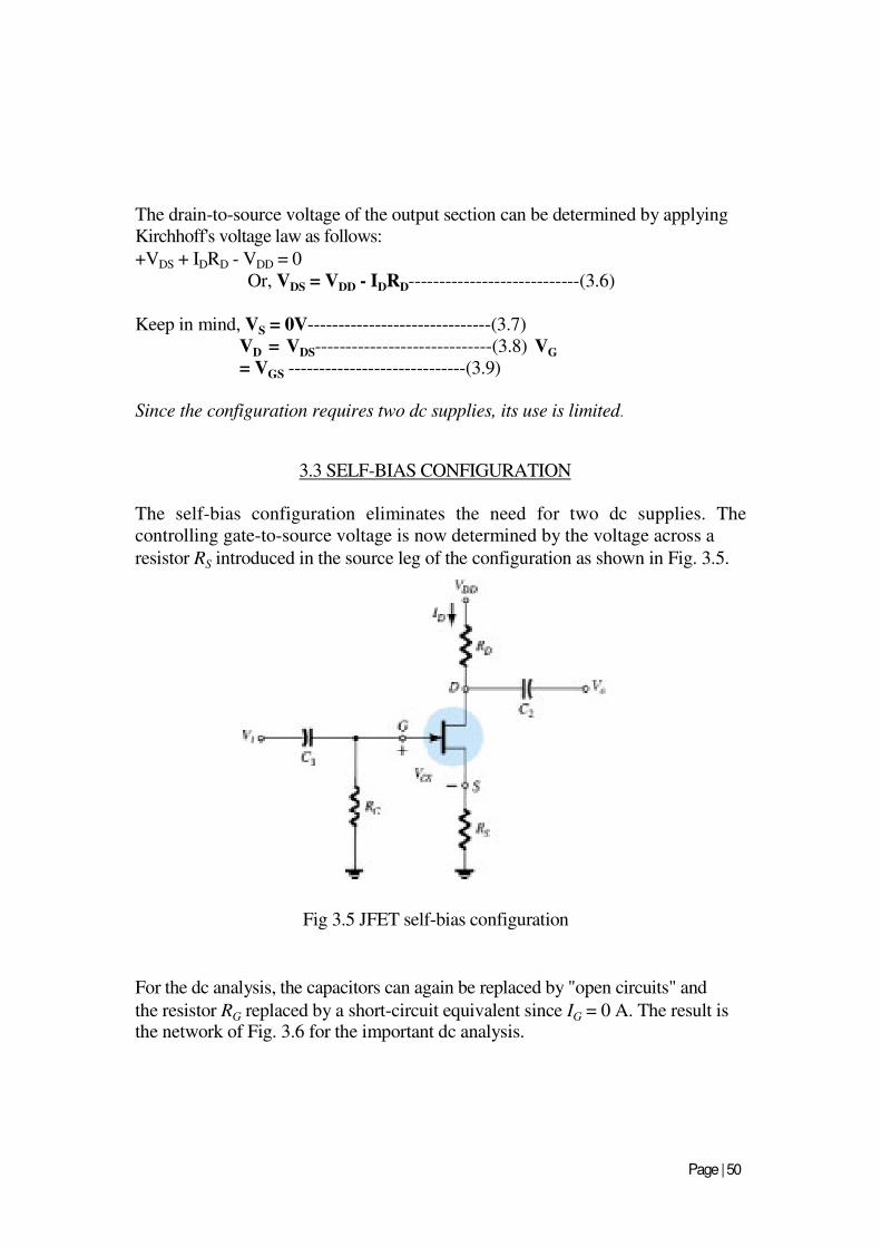
3.3 SELF-BIAS CONFIGURATION
The self-bias configuration eliminates the need for two dc supplies. The
controlling gate-to-source voltage is now determined by the voltage across a
resistor RS introduced in the source leg of the configuration as shown in Fig. 3.5.
Fig 3.5 JFET self-bias configuration
For the dc analysis, the capacitors can again be replaced by "open circuits" and
the resistor RG replaced by a short-circuit equivalent since IG = 0 A. The result is the network of Fig. 3.6 for the important dc analysis.
Page | 50
Anjuman-I-Islam’s Kalsekar Technical Campus, New Panvel
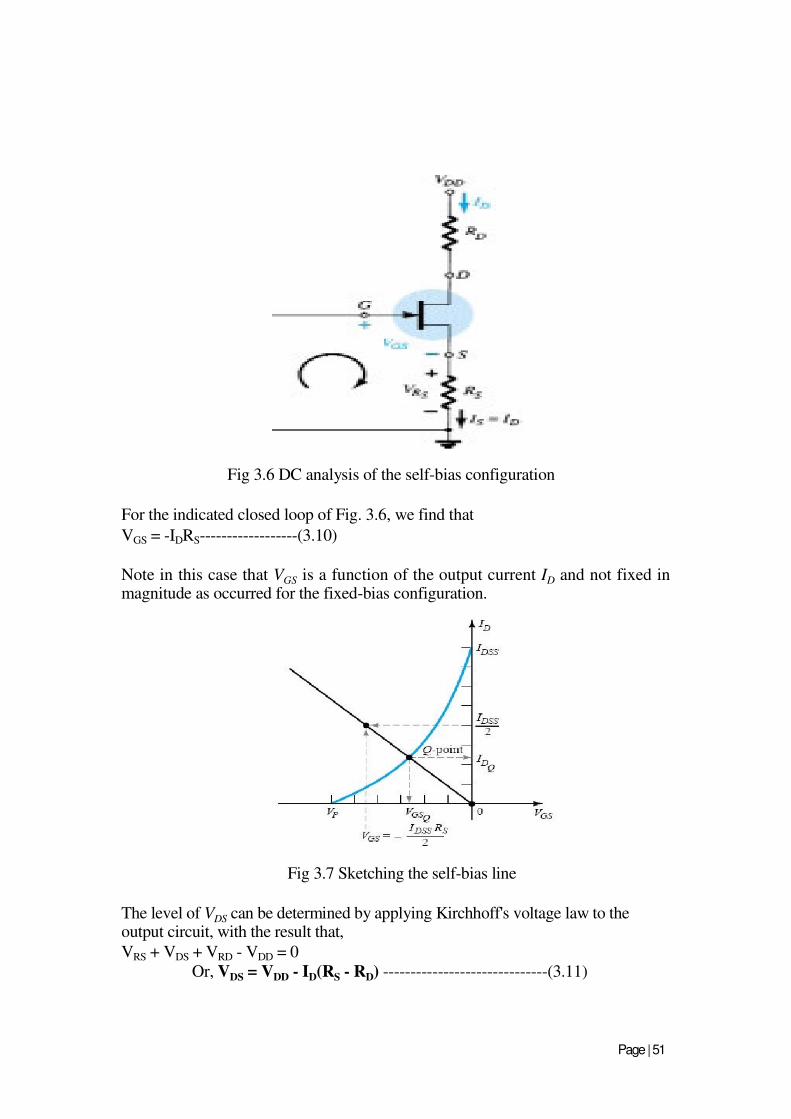
Fig 3.6 DC analysis of the self-bias configuration
For the indicated closed loop of Fig. 3.6, we find that
VGS = -IDRS------------------(3.10)
Note in this case that VGS is a function of the output current ID and not fixed in magnitude as occurred for the fixed-bias configuration.
Fig 3.7 Sketching the self-bias line
The level of VDS can be determined by applying Kirchhoff's voltage law to the output circuit, with the result that,
VRS + VDS + VRD - VDD = 0
Or, VDS = VDD - ID(RS - RD) ------------------------------(3.11)
Page | 51
Anjuman-I-Islam’s Kalsekar Technical Campus, New Panvel
Keep in mind, VS = IDRS-------------------------------------------(3.12)
VG = 0V---------------------------------------------(3.13) VD
= VDS + VS = VDD - VRD ---------------------(3.14)
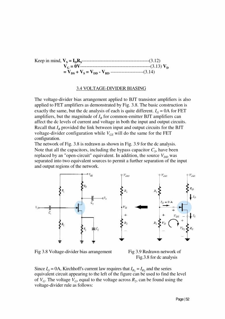
3.4 VOLTAGE-DIVIDER BIASING
The voltage-divider bias arrangement applied to BJT transistor amplifiers is also
applied to FET amplifiers as demonstrated by Fig. 3.8. The basic construction is
exactly the same, but the dc analysis of each is quite different. IG = 0A for FET
amplifiers, but the magnitude of IB for common-emitter BJT amplifiers can affect the dc levels of current and voltage in both the input and output circuits.
Recall that IB provided the link between input and output circuits for the BJT
voltage-divider configuration while VGS will do the same for the FET configuration.
The network of Fig. 3.8 is redrawn as shown in Fig. 3.9 for the dc analysis.
Note that all the capacitors, including the bypass capacitor CS, have been
replaced by an "open-circuit" equivalent. In addition, the source VDD was separated into two equivalent sources to permit a further separation of the input and output regions of the network.
Fig 3.8 Voltage-divider bias arrangement Fig 3.9 Redrawn network of
Fig.3.8 for dc analysis
Since IG = 0A, Kirchhoff's current law requires that IR1 = IR2
and the series equivalent circuit appearing to the left of the figure can be used to find the level
of VG. The voltage VG, equal to the voltage across R2, can be found using the voltage-divider rule as follows:
Page | 52
Anjuman-I-Islam’s Kalsekar Technical Campus, New Panvel
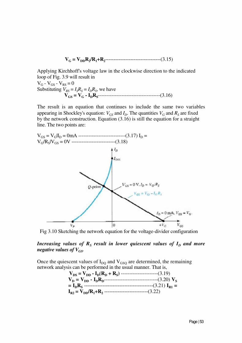
VG = VDDR2/R1+R2---------------------------------(3.15)
Applying Kirchhoff's voltage law in the clockwise direction to the indicated
loop of Fig. 3.9 will result in
VG - VGS - VRS = 0
Substituting VRS = ISRS = IDRS, we have
VGS = VG - IDRS-------------------------------------(3.16)
The result is an equation that continues to include the same two variables
appearing in Shockley's equation: VGS and ID. The quantities VG and RS are fixed by the network construction. Equation (3.16) is still the equation for a straight line. The two points are:
VGS = VG|ID = 0mA ----------------------------(3.17) ID =
VG/RS|VGS = 0V --------------------------(3.18)
Fig 3.10 Sketching the network equation for the voltage-divider configuration
Increasing values of RS result in lower quiescent values of ID and more
negative values of VGS.
Once the quiescent values of IDQ and VGSQ are determined, the remaining network analysis can be performed in the usual manner. That is,
VDS = VDD - ID(RD + RS) ----------------------(3.19)
VD = VDD - IDRD--------------------------------(3.20) VS
= IDRS -----------------------------------------(3.21) IR1 =
IR2 = VDD/R1+R2 --------------------------(3.22)
Page | 53
Anjuman-I-Islam’s Kalsekar Technical Campus, New Panvel
3.5 DEPLETION-TYPE MOSFETs
The similarities in appearance between the transfer curves of JFETs and
depletion-type MOSFETs permit a similar analysis of each in the dc domain.
The primary difference between the two is the fact that depletion-type
MOSFETs permit operating points with positive values of VGS and levels of ID
that exceeds IDSS. In fact, for all the configurations discussed thus far, the analysis is the same if the JFET is replaced by a depletion-type MOSFET.
The only undefined part of the analysis is how to plot Shockley's equation for
positive values of VGS. How far into the region of positive values of VGS and
values of ID greater than IDSS does the transfer curve have to extend? For most situations, this required range will be fairly well defined by the MOSFET parameters and the resulting bias line of the network.
3.6 ENHANCEMENT-TYPE MOSFETs
The transfer characteristics of the enhancement-type MOSFET are quite
different from those encountered for the JFET and depletion-type MOSFETs,
resulting in a graphical solution quite different. First and foremost, recall that
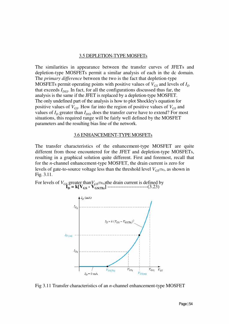
for the n-channel enhancement-type MOSFET, the drain current is zero for
levels of gate-to-source voltage less than the threshold level VGS(Th), as shown in Fig. 3.11.
For levels of VGS greater thanVGS(Th),2the drain current is defined by ID = k[VGS - VGS(Th)] -------------------------(3.23)
Fig 3.11 Transfer characteristics of an n-channel enhancement-type MOSFET
Page | 54
Anjuman-I-Islam’s Kalsekar Technical Campus, New Panvel
Since specification sheets typically provide the threshold voltage and a level of
drain current (ID(on)) and its corresponding level of VGS(on), two points are defined immediately as shown in Fig. 3.11. To complete the curve, the constant
k of Eq. (3.11) must be determined from the specification sheet data by
substituting into Eq. (3.11) and solving for k as follows:
ID = k[VGS - VGS(Th)]2
Or, ID(ON) = k[VGS(ON) - VGS(Th)]
2
k = ID(ON) / [VGS(ON) - VGS(Th)]
2 ----------------------(3.24)
Once k is defined, other levels of ID can be determined for chosen values of VGS. Typically, a point betweenVGS(Th) and VGS(on) and one just greater than VGS(on)
will provide a sufficient number of points to plot Eq. (3.11).
FEEDBACK BIASING ARRANGEMENT
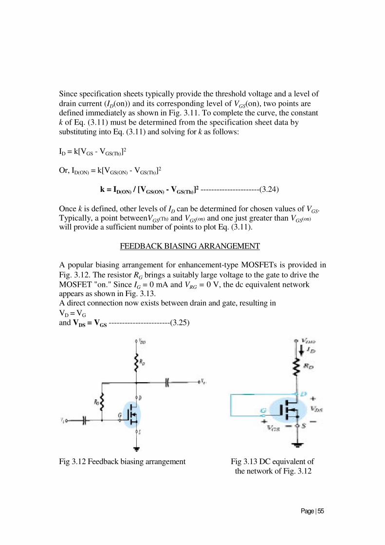
A popular biasing arrangement for enhancement-type MOSFETs is provided in
Fig. 3.12. The resistor RG brings a suitably large voltage to the gate to drive the
MOSFET "on." Since IG = 0 mA and VRG = 0 V, the dc equivalent network appears as shown in Fig. 3.13. A direct connection now exists between drain and gate, resulting in
VD = VG
and VDS = VGS -----------------------(3.25)
Fig 3.12 Feedback biasing arrangement Fig 3.13 DC equivalent of
the network of Fig. 3.12
Page | 55
Anjuman-I-Islam’s Kalsekar Technical Campus, New Panvel
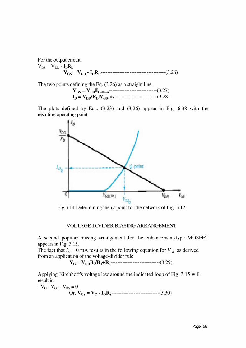
For the output circuit,
VDS = VDD - IDRD
VGS = VDD - IDRD--------------------------------------(3.26)
The two points defining the Eq. (3.26) as a straight line,
VGS = VDD|ID=0mA----------------------------(3.27)
ID = VDD/RD|VGS= 0V-------------------------(3.28)
The plots defined by Eqs. (3.23) and (3.26) appear in Fig. 6.38 with the
resulting operating point.
Fig 3.14 Determining the Q-point for the network of Fig. 3.12
VOLTAGE-DIVIDER BIASING ARRANGEMENT
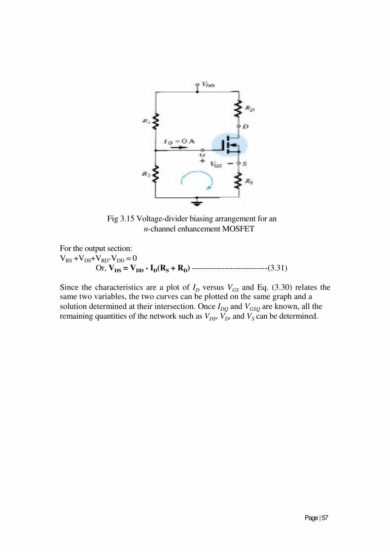
A second popular biasing arrangement for the enhancement-type MOSFET
appears in Fig. 3.15.
The fact that IG = 0 mA results in the following equation for VGG as derived from an application of the voltage-divider rule:
VG = VDDR2/R1+R2-----------------------------(3.29)
Applying Kirchhoff's voltage law around the indicated loop of Fig. 3.15 will
result in,
+VG - VGS - VRS = 0
Or, VGS = VG - IDRS----------------------------(3.30)
Page | 56
Anjuman-I-Islam’s Kalsekar Technical Campus, New Panvel
Fig 3.15 Voltage-divider biasing arrangement for an
n-channel enhancement MOSFET
For the output section:
VRS +VDS+VRD-VDD = 0
Or, VDS = VDD - ID(RS + RD) ----------------------------(3.31)
Since the characteristics are a plot of ID versus VGS and Eq. (3.30) relates the same two variables, the two curves can be plotted on the same graph and a
solution determined at their intersection. Once IDQ and VGSQ are known, all the
remaining quantities of the network such as VDS, VD, and VS can be determined.
Page | 57
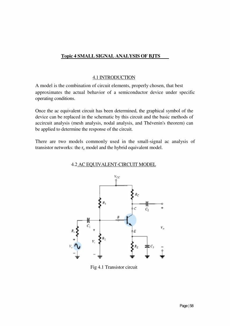
Anjuman-I-Islam’s Kalsekar Technical Campus, New Panvel
Topic 4 SMALL SIGNAL ANALYSIS OF BJTS
4.1 INTRODUCTION
A model is the combination of circuit elements, properly chosen, that best
approximates the actual behavior of a semiconductor device under specific
operating conditions.
Once the ac equivalent circuit has been determined, the graphical symbol of the
device can be replaced in the schematic by this circuit and the basic methods of
accircuit analysis (mesh analysis, nodal analysis, and Thévenin's theorem) can
be applied to determine the response of the circuit.
There are two models commonly used in the small-signal ac analysis of
transistor networks: the re model and the hybrid equivalent model.
4.2 AC EQUIVALENT-CIRCUIT MODEL
Fig 4.1 Transistor circuit
Page | 58
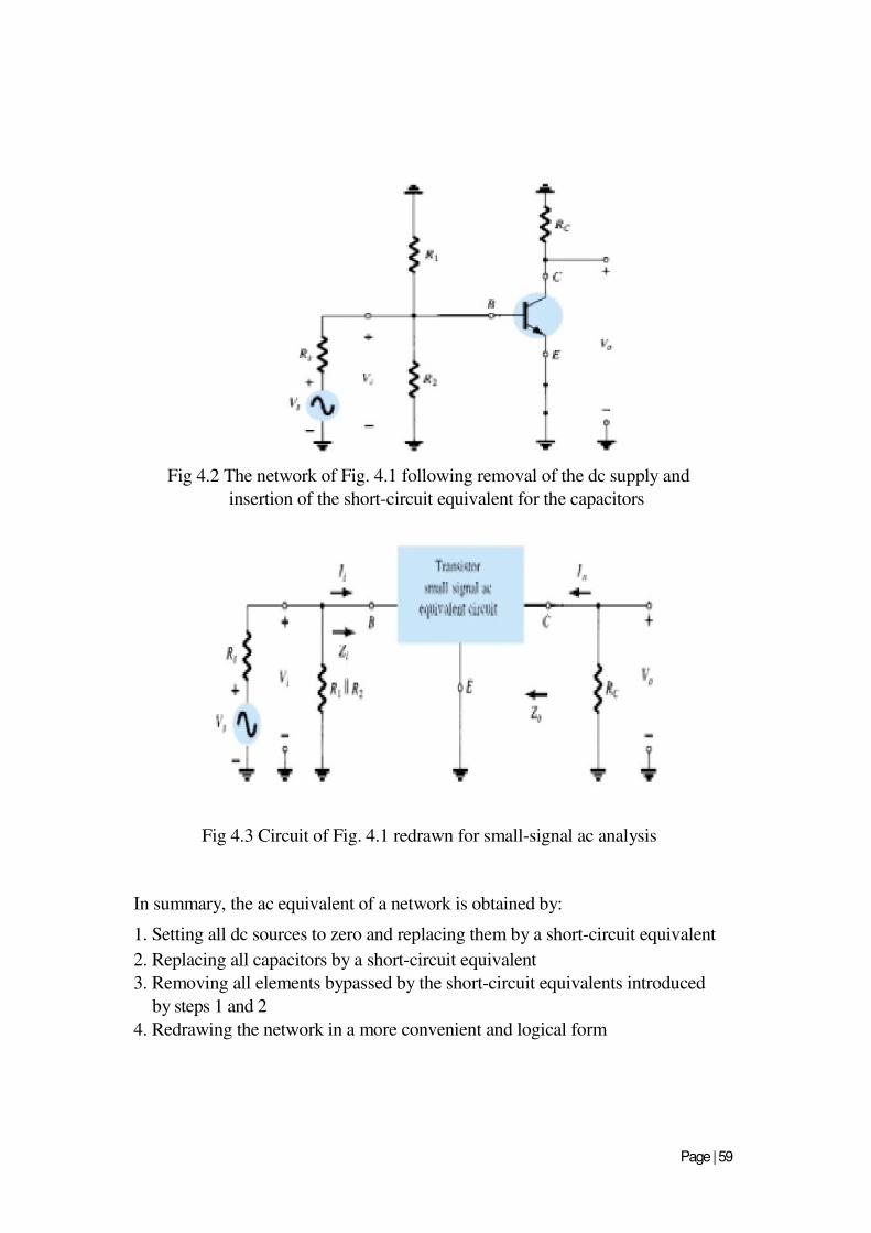
Anjuman-I-Islam’s Kalsekar Technical Campus, New Panvel
Fig 4.2 The network of Fig. 4.1 following removal of the dc supply and
insertion of the short-circuit equivalent for the capacitors
Fig 4.3 Circuit of Fig. 4.1 redrawn for small-signal ac analysis
In summary, the ac equivalent of a network is obtained by:
1. Setting all dc sources to zero and replacing them by a short-circuit equivalent
2. Replacing all capacitors by a short-circuit equivalent
3. Removing all elements bypassed by the short-circuit equivalents introduced
by steps 1 and 2
4. Redrawing the network in a more convenient and logical form
Page | 59
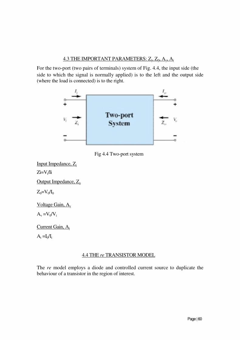
Anjuman-I-Islam’s Kalsekar Technical Campus, New Panvel
4.3 THE IMPORTANT PARAMETERS: Zi, Z0, Av, Ai
For the two-port (two pairs of terminals) system of Fig. 4.4, the input side (the
side to which the signal is normally applied) is to the left and the output side
(where the load is connected) is to the right.
Input Impedance, Zi
Zi=Vi/Ii
Output Impedance, Zo
Z0=V0/I0
Voltage Gain, Av Av =V0/Vi
Current Gain, Ai Ai =I0/Ii
Fig 4.4 Two-port system
4.4 THE re TRANSISTOR MODEL
The re model employs a diode and controlled current source to duplicate the
behaviour of a transistor in the region of interest.
Page | 60
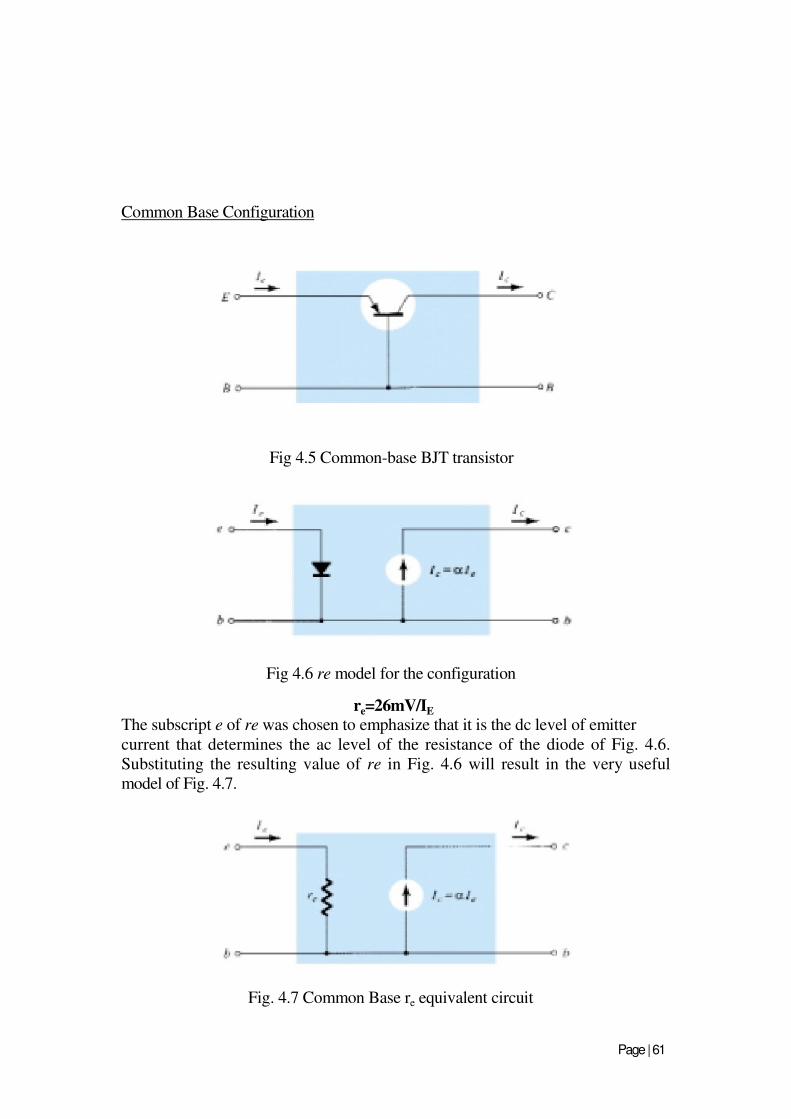
Anjuman-I-Islam’s Kalsekar Technical Campus, New Panvel
Common Base Configuration
Fig 4.5 Common-base BJT transistor
Fig 4.6 re model for the configuration
re=26mV/IE
The subscript e of re was chosen to emphasize that it is the dc level of emitter
current that determines the ac level of the resistance of the diode of Fig. 4.6.
Substituting the resulting value of re in Fig. 4.6 will result in the very useful
model of Fig. 4.7.
Fig. 4.7 Common Base re equivalent circuit
Page | 61
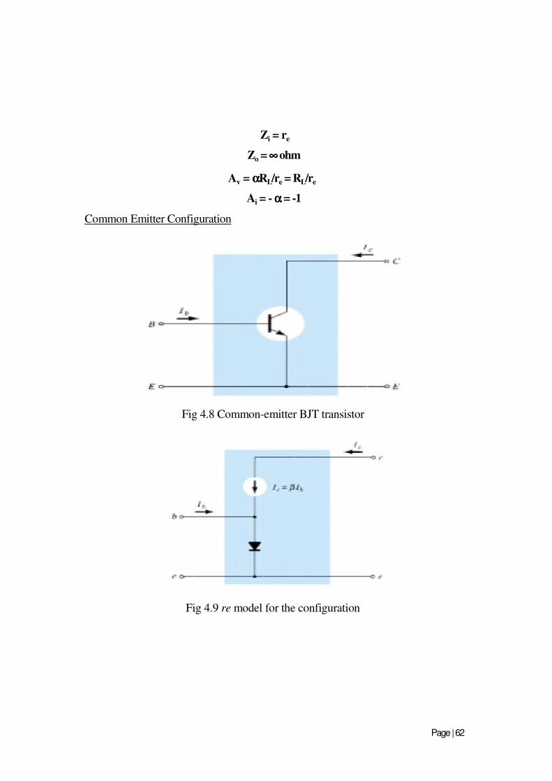
Anjuman-I-Islam’s Kalsekar Technical Campus, New Panvel
Zi = re
Zo = ∞∞∞∞ ohm
Av = ααααRL/re = RL/re
Ai = - αααα = -1
Common Emitter Configuration
Fig 4.8 Common-emitter BJT transistor
Fig 4.9 re model for the configuration
Page | 62
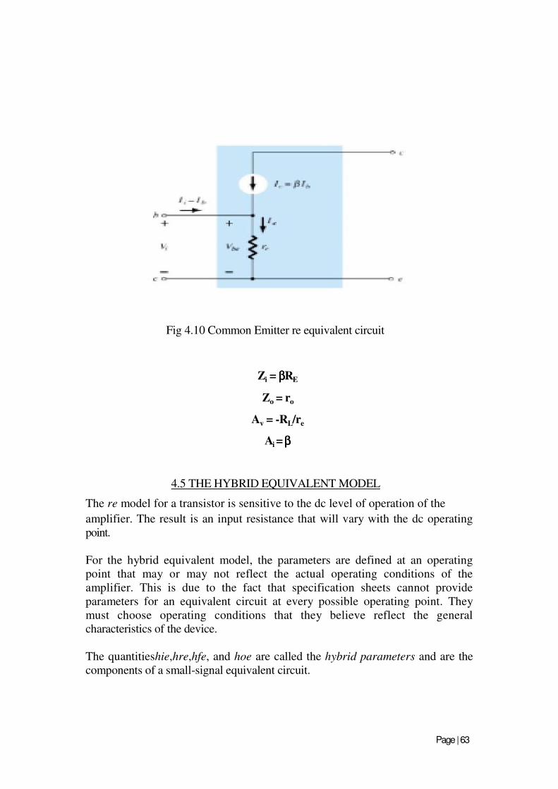
Anjuman-I-Islam’s Kalsekar Technical Campus, New Panvel
Fig 4.10 Common Emitter re equivalent circuit
Zi = ββββRE
Zo = ro
Av = -RL/re
Ai = ββββ
4.5 THE HYBRID EQUIVALENT MODEL
The re model for a transistor is sensitive to the dc level of operation of the
amplifier. The result is an input resistance that will vary with the dc operating
point.
For the hybrid equivalent model, the parameters are defined at an operating
point that may or may not reflect the actual operating conditions of the
amplifier. This is due to the fact that specification sheets cannot provide
parameters for an equivalent circuit at every possible operating point. They
must choose operating conditions that they believe reflect the general
characteristics of the device.
The quantitieshie,hre,hfe, and hoe are called the hybrid parameters and are the
components of a small-signal equivalent circuit.
Page | 63
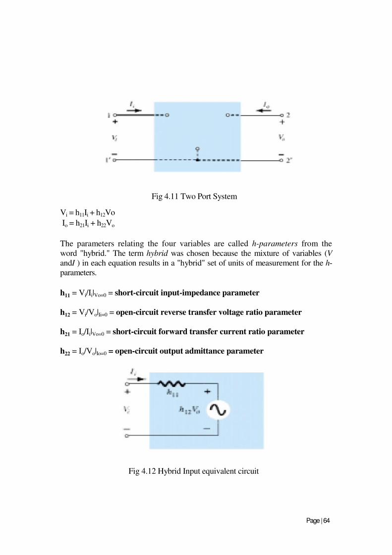
Anjuman-I-Islam’s Kalsekar Technical Campus, New Panvel
Fig 4.11 Two Port System
Vi = h11Ii + h12Vo
Io = h21Ii + h22Vo
The parameters relating the four variables are called h-parameters from the
word "hybrid." The term hybrid was chosen because the mixture of variables (V
andI ) in each equation results in a "hybrid" set of units of measurement for the h-
parameters.
h11 = Vi/Ii|Vo=0 = short-circuit input-impedance parameter
h12 = Vi/Vo|Ii=0 = open-circuit reverse transfer voltage ratio parameter
h21 = Io/Ii|Vo=0 = short-circuit forward transfer current ratio parameter
h22 = Io/Vo|Io=0 = open-circuit output admittance parameter
Fig 4.12 Hybrid Input equivalent circuit
Page | 64
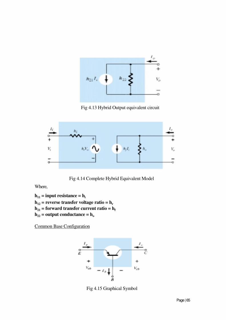
Anjuman-I-Islam’s Kalsekar Technical Campus, New Panvel
Fig 4.13 Hybrid Output equivalent circuit
Fig 4.14 Complete Hybrid Equivalent Model
Where,
h11 = input resistance = hi
h12 = reverse transfer voltage ratio = hr
h21 = forward transfer current ratio = hf
h22 = output conductance = ho
Common Base Configuration
Fig 4.15 Graphical Symbol
Page | 65
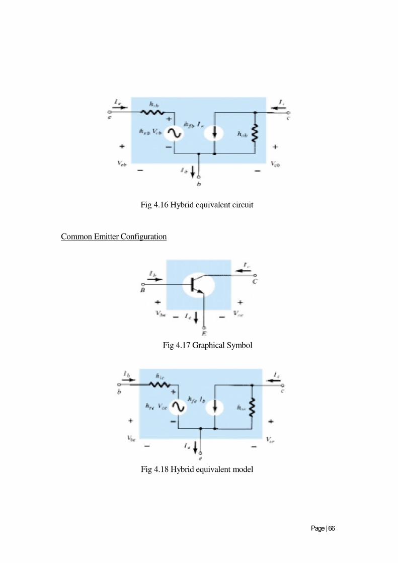
Anjuman-I-Islam’s Kalsekar Technical Campus, New Panvel
Fig 4.16 Hybrid equivalent circuit
Common Emitter Configuration
Fig 4.17 Graphical Symbol
Fig 4.18 Hybrid equivalent model
Page | 66
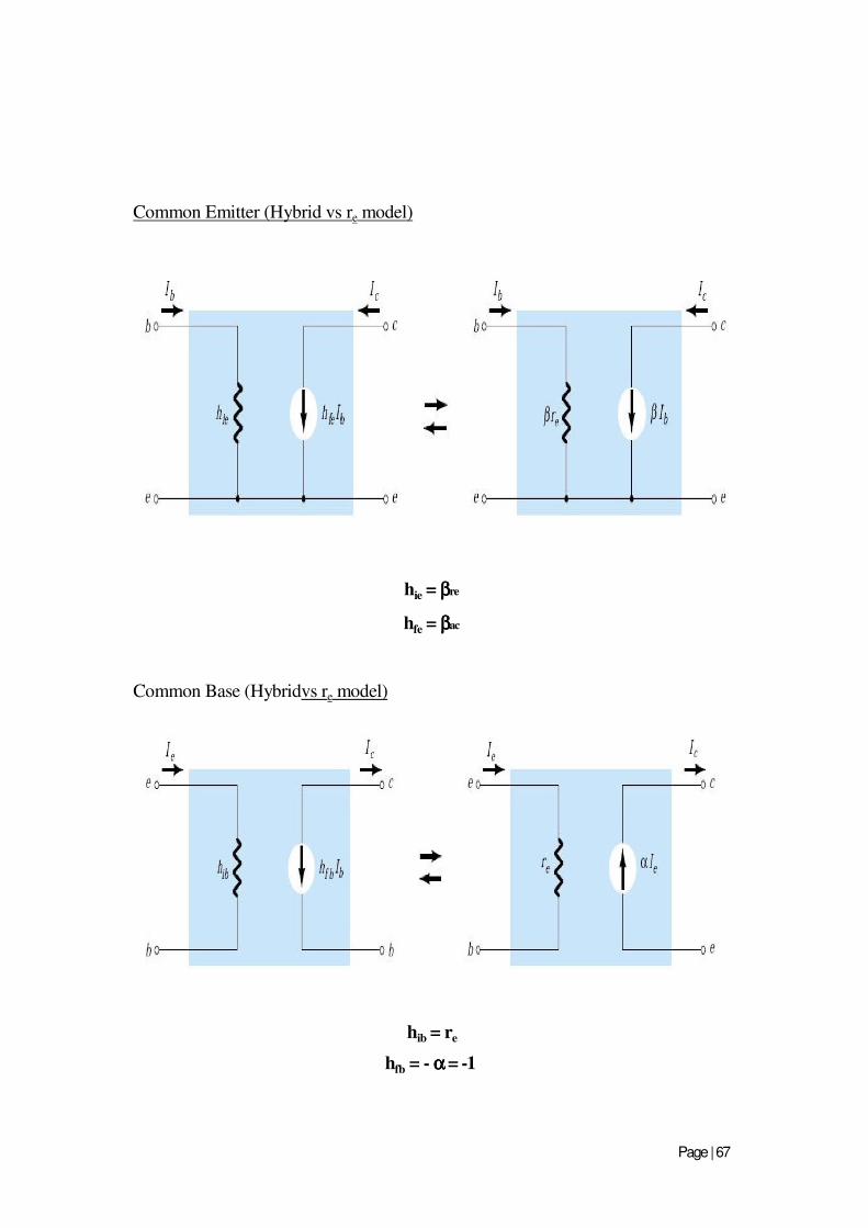
Anjuman-I-Islam’s Kalsekar Technical Campus, New Panvel
Common Emitter (Hybrid vs re model)
hie = ββββre
hfe = ββββac
Common Base (Hybridvs re model)
hib = re
hfb = - αααα = -1
Page | 67
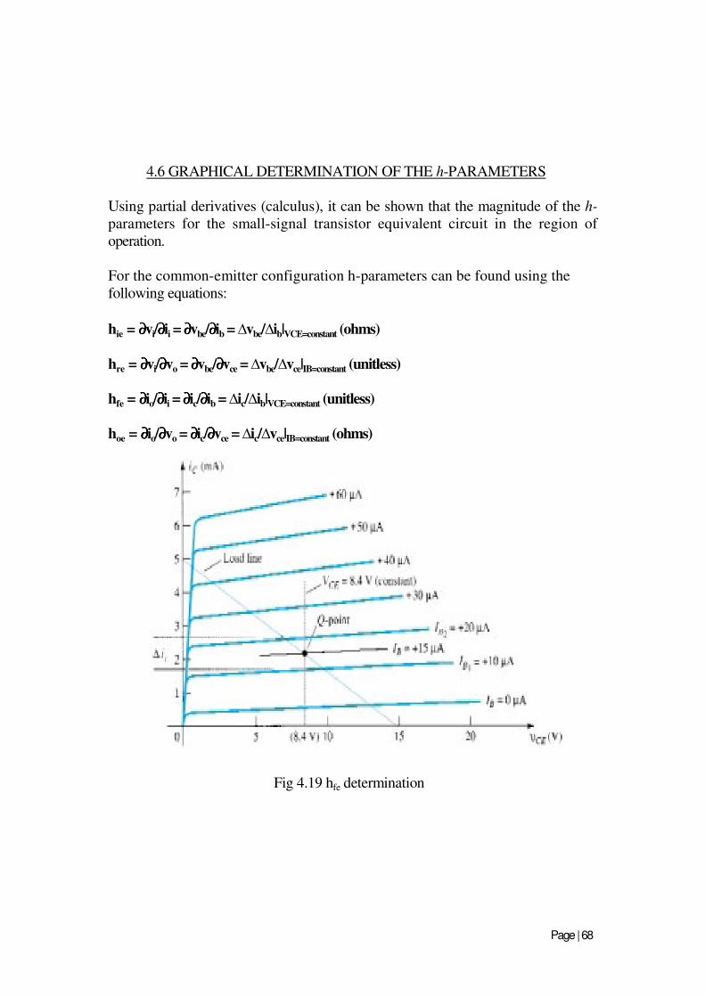
Anjuman-I-Islam’s Kalsekar Technical Campus, New Panvel
4.6 GRAPHICAL DETERMINATION OF THE h-PARAMETERS
Using partial derivatives (calculus), it can be shown that the magnitude of the h-
parameters for the small-signal transistor equivalent circuit in the region of
operation.
For the common-emitter configuration h-parameters can be found using the
following equations:
hie = ∂∂∂∂vi/∂∂∂∂ii = ∂∂∂∂vbe/∂∂∂∂ib = ∆vbe/∆ib|VCE=constant (ohms) hre = ∂∂∂∂vi/∂∂∂∂vo = ∂∂∂∂vbe/∂∂∂∂vce = ∆vbe/∆vce|IB=constant (unitless) hfe = ∂∂∂∂io/∂∂∂∂ii = ∂∂∂∂ic/∂∂∂∂ib = ∆ic/∆ib|VCE=constant (unitless) hoe = ∂∂∂∂io/∂∂∂∂vo = ∂∂∂∂ic/∂∂∂∂vce = ∆ic/∆vce|IB=constant (ohms)
Fig 4.19 hfe determination
Page | 68
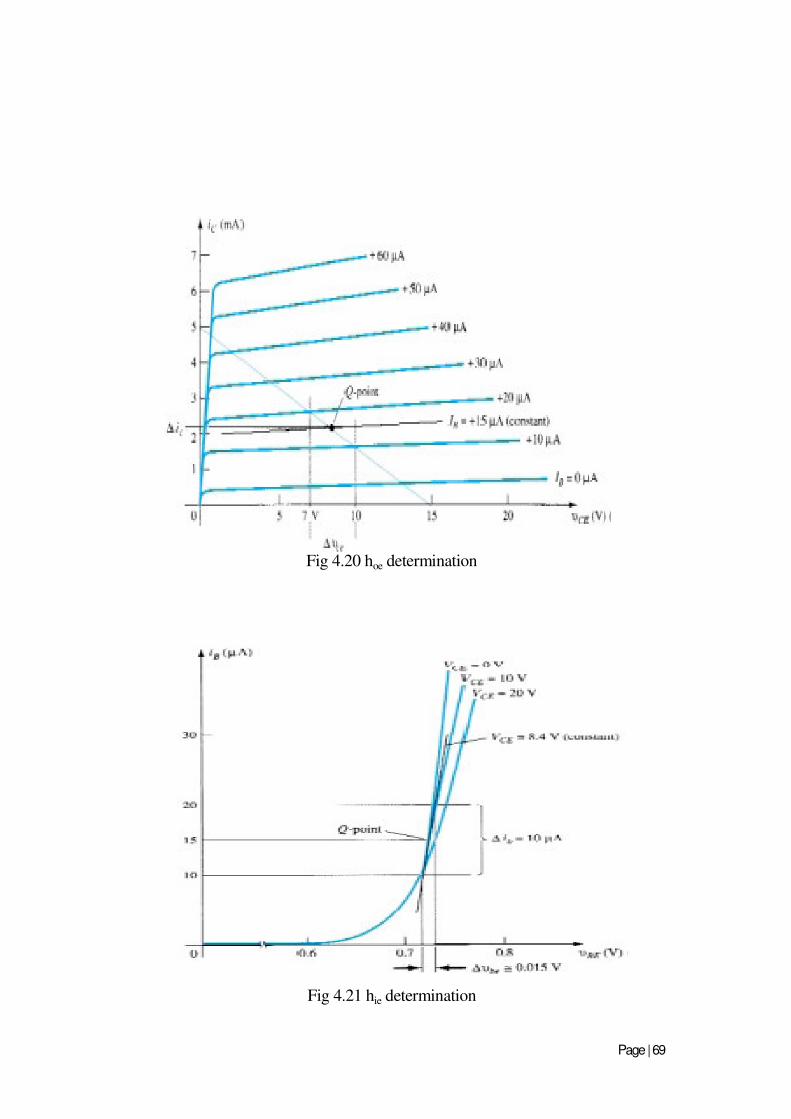
Anjuman-I-Islam’s Kalsekar Technical Campus, New Panvel
Fig 4.20 hoe determination
Fig 4.21 hie determination
Page | 69
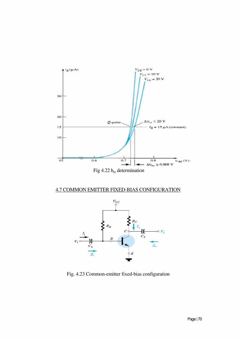
Anjuman-I-Islam’s Kalsekar Technical Campus, New Panvel
Fig 4.22 hre determination
4.7 COMMON EMITTER FIXED-BIAS CONFIGURATION
Fig. 4.23 Common-emitter fixed-bias configuration
Page | 70
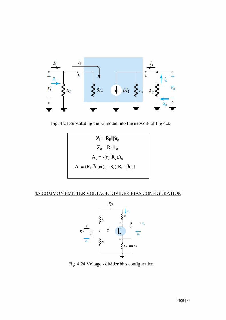
Anjuman-I-Islam’s Kalsekar Technical Campus, New Panvel
Fig. 4.24 Substituting the re model into the network of Fig 4.23
Zi = RB||βre
Zo = RC||ro
Av = -(ro||Rc)/re
Ai = (RBβro)/((ro+Rc)(RB+βre))
4.8 COMMON EMITTER VOLTAGE-DIVIDER BIAS CONFIGURATION
Fig. 4.24 Voltage - divider bias configuration
Page | 71
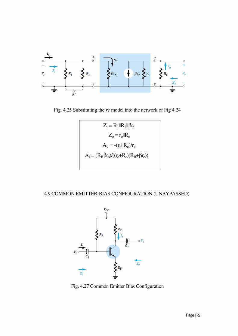
Anjuman-I-Islam’s Kalsekar Technical Campus, New Panvel
Fig. 4.25 Substituting the re model into the network of Fig 4.24
Zi = R1||R2||βre
Zo = ro||Rc
Av = -(ro||Rc)/re
Ai = (RBβro)/((ro+Rc)(RB+βre))
4.9 COMMON EMITTER-BIAS CONFIGURATION (UNBYPASSED)
Fig. 4.27 Common Emitter Bias Configuration
Page | 72
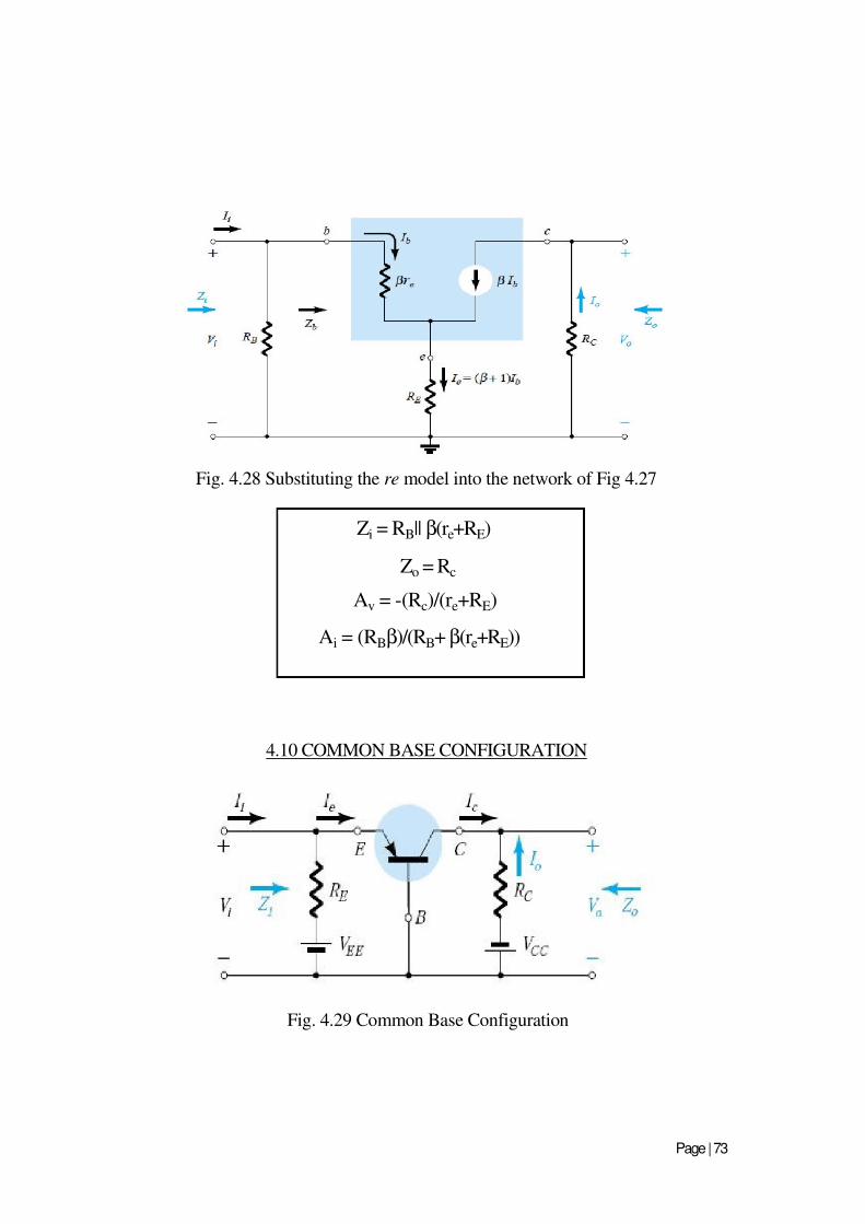
Anjuman-I-Islam’s Kalsekar Technical Campus, New Panvel
Fig. 4.28 Substituting the re model into the network of Fig 4.27
Zi = RB|| β(re+RE)
Zo = Rc
Av = -(Rc)/(re+RE)
Ai = (RBβ)/(RB+ β(re+RE))
4.10 COMMON BASE CONFIGURATION
Fig. 4.29 Common Base Configuration
Page | 73
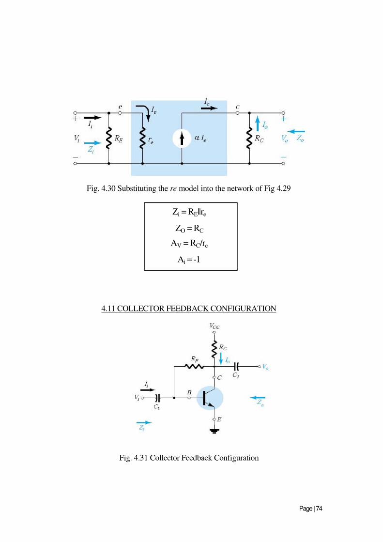
Anjuman-I-Islam’s Kalsekar Technical Campus, New Panvel
Fig. 4.30 Substituting the re model into the network of Fig 4.29
Zi = RE||re
ZO = RC
AV = RC/re
Ai = -1
4.11 COLLECTOR FEEDBACK CONFIGURATION
Fig. 4.31 Collector Feedback Configuration
Page | 74
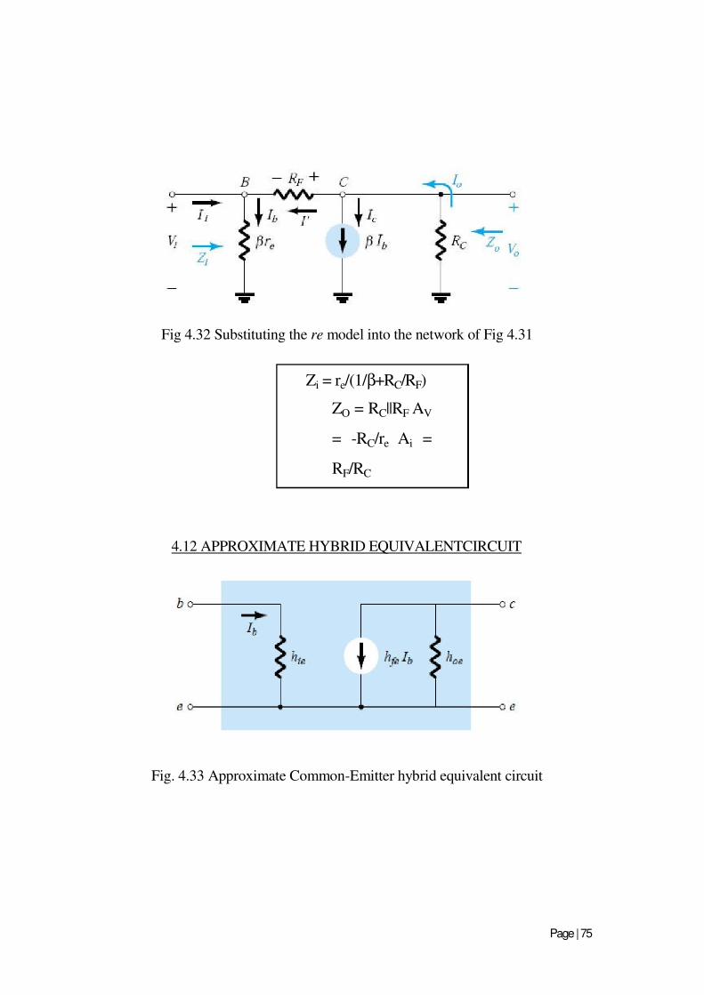
Anjuman-I-Islam’s Kalsekar Technical Campus, New Panvel
Fig 4.32 Substituting the re model into the network of Fig 4.31
Zi = re/(1/β+RC/RF)
ZO = RC||RF AV
= -RC/re Ai =
RF/RC
4.12 APPROXIMATE HYBRID EQUIVALENTCIRCUIT
Fig. 4.33 Approximate Common-Emitter hybrid equivalent circuit
Page | 75
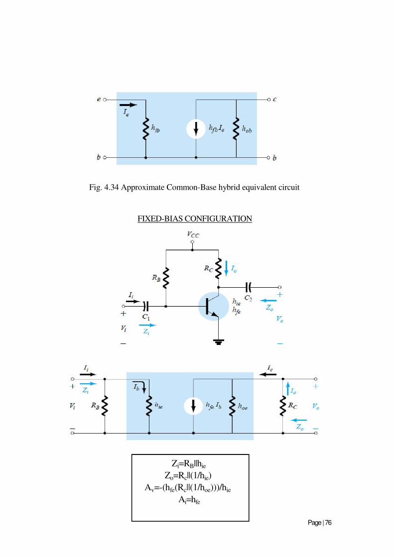
Anjuman-I-Islam’s Kalsekar Technical Campus, New Panvel
Fig. 4.34 Approximate Common-Base hybrid equivalent circuit
FIXED-BIAS CONFIGURATION
Zi=RB||hie
Zo=Rc||(1/hie)
Av=-(hfe(Rc||(1/hoe)))/hie
Ai=hfe
Page | 76
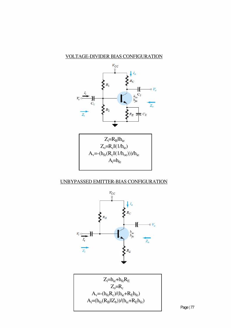
Anjuman-I-Islam’s Kalsekar Technical Campus, New Panvel
VOLTAGE-DIVIDER BIAS CONFIGURATION
Zi=RB||hie
Zo=Rc||(1/hie)
Av=-(hfe(Rc||(1/hoe)))/hie
Ai=hfe
UNBYPASSED EMITTER-BIAS CONFIGURATION
Zi=hie+hfeRE
Zo=Rc
Av=-(hfeRc)/(hie+REhfe)
Ai=(hfe(RB||Zb))/(hie+REhfe)
Page | 77
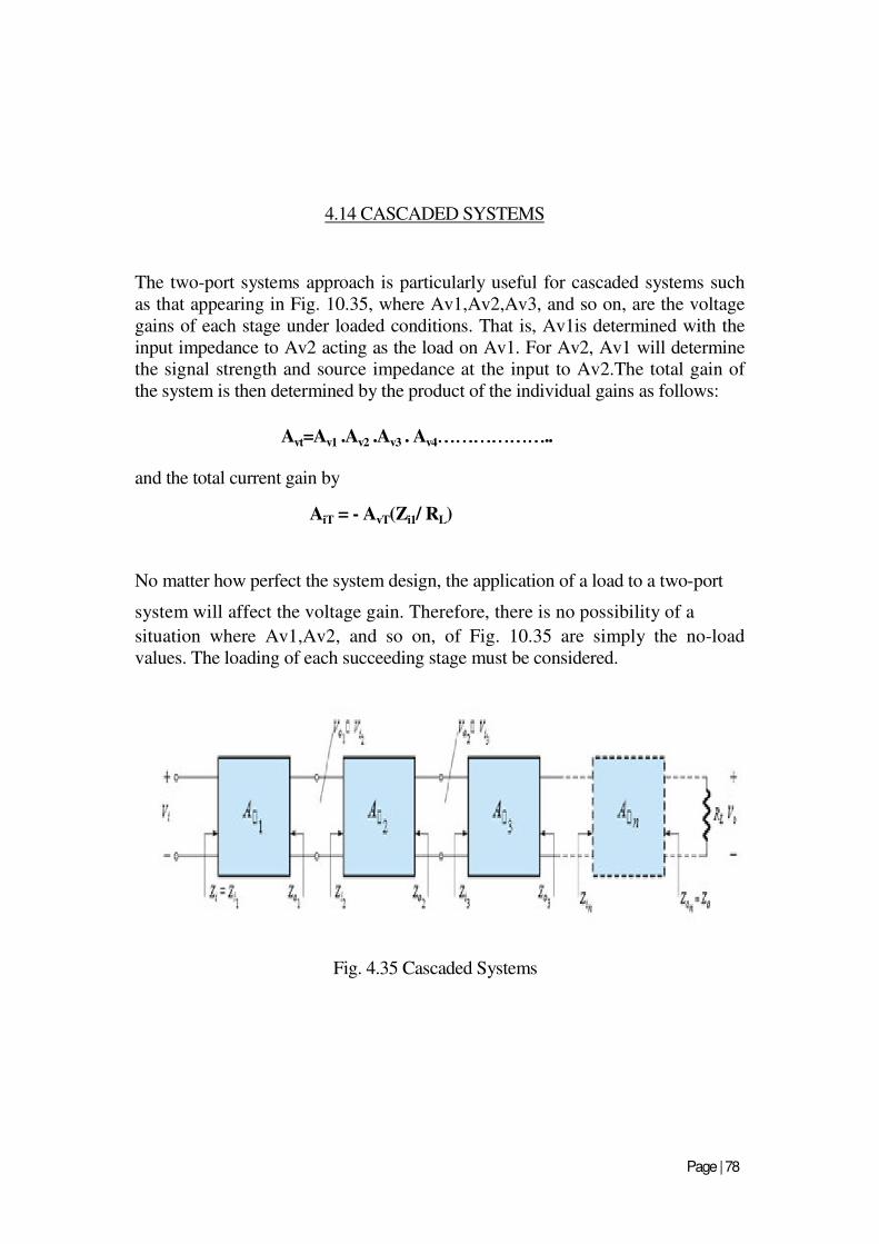
Anjuman-I-Islam’s Kalsekar Technical Campus, New Panvel
4.14 CASCADED SYSTEMS
The two-port systems approach is particularly useful for cascaded systems such
as that appearing in Fig. 10.35, where Av1,Av2,Av3, and so on, are the voltage
gains of each stage under loaded conditions. That is, Av1is determined with the
input impedance to Av2 acting as the load on Av1. For Av2, Av1 will determine
the signal strength and source impedance at the input to Av2.The total gain of
the system is then determined by the product of the individual gains as follows:
Avt=Av1 .Av2 .Av3 . Av4………………………………………………………………..
and the total current gain by
AiT = - AvT(Zi1/ RL)
No matter how perfect the system design, the application of a load to a two-port
system will affect the voltage gain. Therefore, there is no possibility of a
situation where Av1,Av2, and so on, of Fig. 10.35 are simply the no-load
values. The loading of each succeeding stage must be considered.
Fig. 4.35 Cascaded Systems
Page | 78
Anjuman-I-Islam’s Kalsekar Technical Campus, New Panvel
Topic 5 SMALL SIGNAL ANALYSIS OF FETS
5.1 INTRODUCTION
Field-effect transistor amplifiers provide an excellent voltage gain with the
added feature of a high input impedance. They are also considered low-power
consumption configurations with good frequency range and minimal size and
weight. Both JFET and depletion MOSFET devices can be used to design
amplifiers having similar voltage gains. The depletion MOSFET circuit,
however, has a much higher input impedance than a similar JFET configuration.
While a BJT device controls a large output (collector) current by means of a
relatively small input (base) current, the FET device controls an output (drain)
current by means of a small input (gate-voltage) voltage. In general, therefore,
the BJT is a current-controlled device and the FET is a voltage-controlled
device. In both cases, however, note that the output current is the controlled
variable. Because of the high input characteristic of FETs, the ac equivalent
model is somewhat simpler than that employed for BJTs. While the BJT had an
amplification factor β (beta), the FET has a transconductance factor, gm. The FET can be used as a linear amplifier or as a digital device in logic circuits.
In fact, the enhancement MOSFET is quite popular in digital circuitry,
especially in CMOS circuits that require very low power consumption. FET
devices are also widely used in high-frequency applications and in buffering
(interfacing) applications.
While the common-source configuration is the most popular providing an
inverted, amplified signal, one also finds common-drain (source-follower)
circuits providing unity gain with no inversion and common-gate circuits
providing gain with no inversion. As with BJT amplifiers, the important circuit
features described in this chapter include voltage gain, input impedance, and
output impedance. Due to the very high input impedance, the input current is
generally assumed to be 0 µA and the current gain is an undefined quantity.
While the voltage gain of an FET amplifier is generally less than that obtained
using a BJT amplifier, the FET amplifier provides much higher input impedance
than that of a BJT configuration. Output impedance values are comparable for
both BJT and FET circuits.
5.2 FET SMALL-SIGNAL MODEL
The ac analysis of an FET configuration requires that a small-signal ac model
for the FET be developed. A major component of the ac model will reflect the
Page | 79
Anjuman-I-Islam’s Kalsekar Technical Campus, New Panvel
fact that an ac voltage applied to the input gate-to-source terminals will control
the level of current from drain to source.
The gate-to-source voltage controls the drain-to-source (channel) current of
an FET.
A dc gate-to-source voltage controlled the level of dc drain current through a
relationship known as Shockley's equation: ID=IDSS(VGS-Vp)2
The change in collector current that will result from a change in gate-to-source
voltage can be determined using the transconductance factorgm in the
following manner: ∆ID =gm ∆VGS
The prefix trans- in the terminology applied togm reveals that it establishes a
relationship between an output and input quantity. The root word conductance
was chosen becausegm is determined by a voltage-to-current ratio similar to the
ratio that defines the conductance of a resistor G = 1/R = I/V or, gm=∆ID/∆VGS
5.3. GRAPHICAL DETERMINATION OF gm
gm=m=∆y/∆x=∆ID/∆VGS
5.4 MATHEMATICAL DEFINITION OF gm
gm= 2 IDSS/Vp[1-VGS/Vp]
Page | 80
Anjuman-I-Islam’s Kalsekar Technical Campus, New Panvel
gm0 =2 IDSS/Vp
gm=gm0[1-VGS/Vp]
Impact of ID on gm :gm=gm0[1-VGS/Vp] = gm0(√ID/IDSS)
FET Input Impedance zi: Zi(FET) = ∞Ω
FET Output Impedance zo: Zo(FET) = rd
5.4 FET AC EQUIVALENT CIRCUIT
a model for the FET transistor in the ac domain can be constructed. The control
of Id byVgs is included as a current sourcegmVgs connected from drain to
source as shown in Fig. 5.1. The current source has its arrow pointing from
drain to source to establish a 180° phase shift between output and input voltages
as will occur in actual operation.
Fig. 5.1 FET AC Equivalent circuit
The input impedance is represented by the open circuit at the input terminals
and the output impedance by the resistorrd from drain to source. Note that the
gate to source voltage is now represented byVgs (lower-case subscripts) to
distinguish it from dc levels. In addition, take note of the fact that the source is
common to both input and output circuits while the gate and drain terminals are
only in "touch" through the controlled current sourcegmVgs.
In situations whererd is ignored (assumed sufficiently large to other elements of
the network to be approximated by an open circuit), the equivalent circuit is
Page | 81
Anjuman-I-Islam’s Kalsekar Technical Campus, New Panvel
simply a current source whose magnitude is controlled by the signalVgs and
parametergm— clearly a voltage-controlled device.
5.5 FIXED BIAS CIRCUIT
Zi = RG
ZO = RD||rd
Av = -gm(RD||rd)
Page | 82
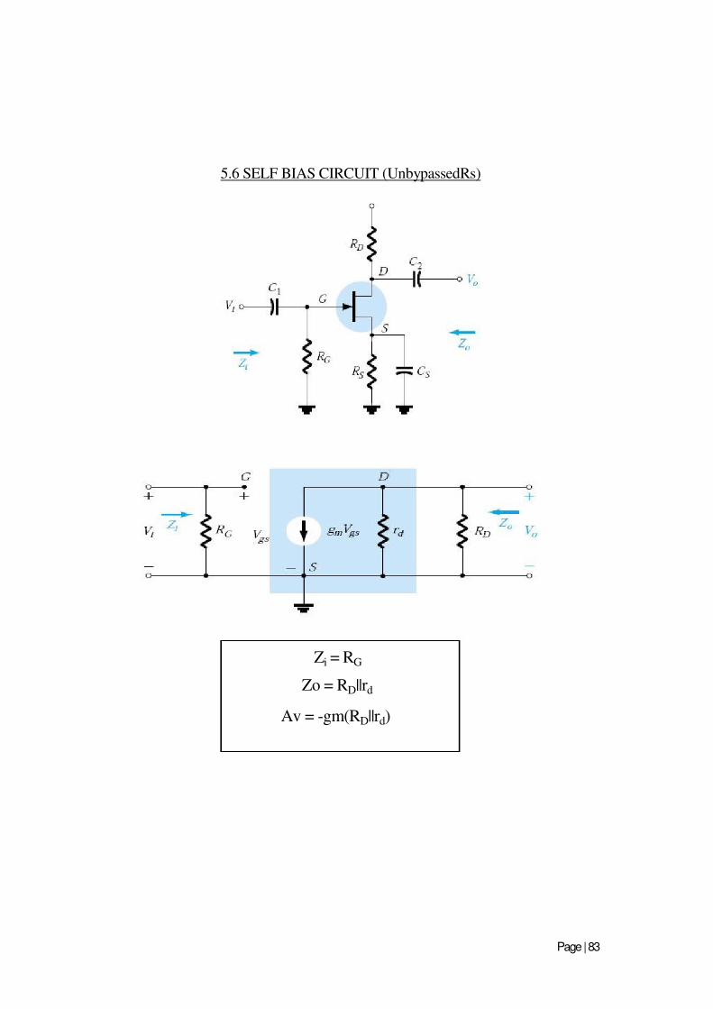
Anjuman-I-Islam’s Kalsekar Technical Campus, New Panvel
5.6 SELF BIAS CIRCUIT (UnbypassedRs)
Zi = RG
Zo = RD||rd
Av = -gm(RD||rd)
Page | 83
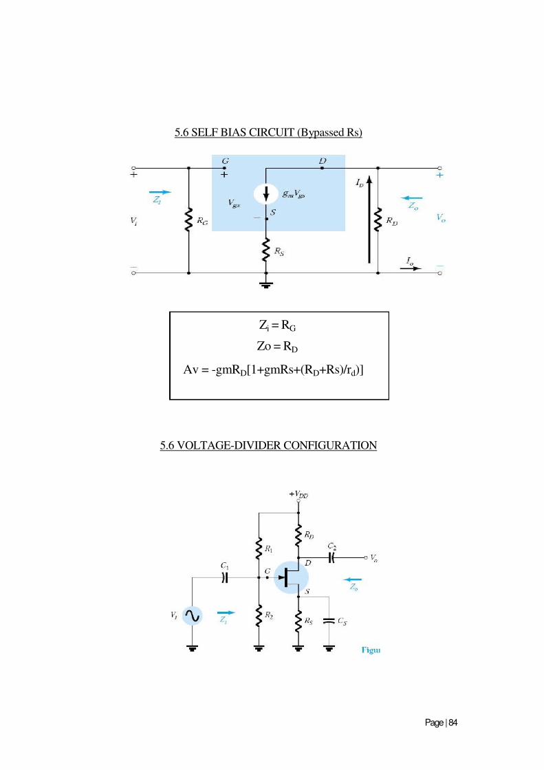
Anjuman-I-Islam’s Kalsekar Technical Campus, New Panvel
5.6 SELF BIAS CIRCUIT (Bypassed Rs)
Zi = RG
Zo = RD
Av = -gmRD[1+gmRs+(RD+Rs)/rd)]
5.6 VOLTAGE-DIVIDER CONFIGURATION
Page | 84
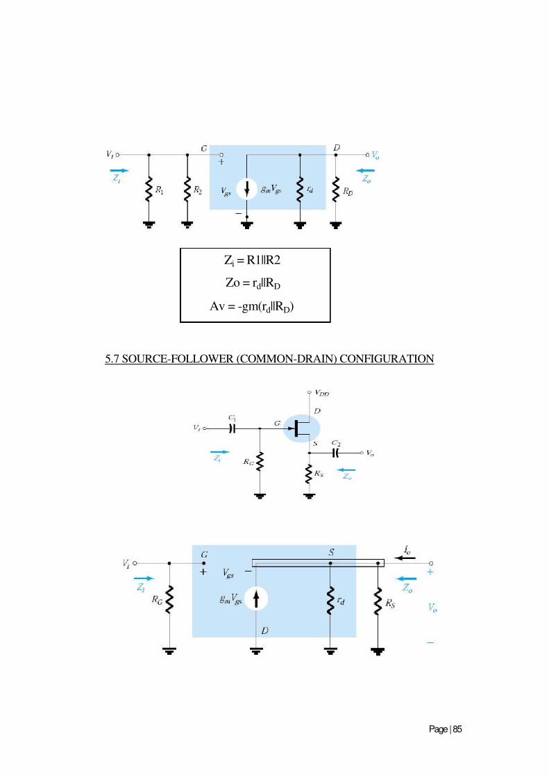
Anjuman-I-Islam’s Kalsekar Technical Campus, New Panvel
Zi = R1||R2
Zo = rd||RD
Av = -gm(rd||RD)
5.7 SOURCE-FOLLOWER (COMMON-DRAIN) CONFIGURATION
Page | 85
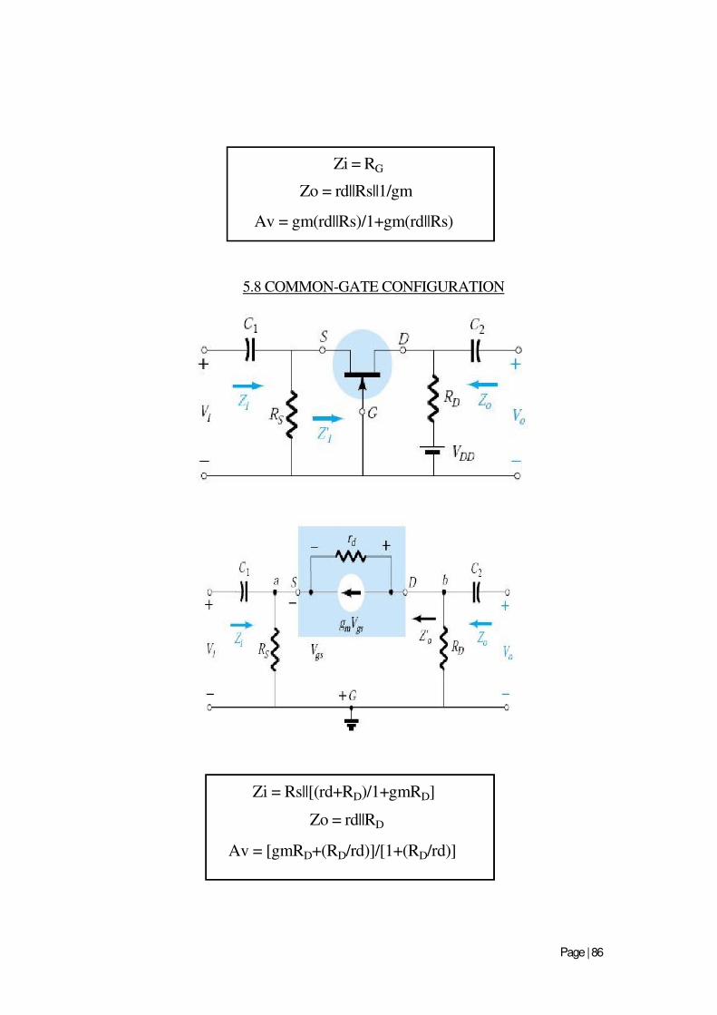
Anjuman-I-Islam’s Kalsekar Technical Campus, New Panvel
Zi = RG
Zo = rd||Rs||1/gm
Av = gm(rd||Rs)/1+gm(rd||Rs)
5.8 COMMON-GATE CONFIGURATION
Zi = Rs||[(rd+RD)/1+gmRD]
Zo = rd||RD
Av = [gmRD+(RD/rd)]/[1+(RD/rd)]
Page | 86
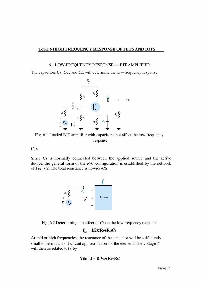
Anjuman-I-Islam’s Kalsekar Technical Campus, New Panvel
Topic 6 HIGH FREQUENCY RESPONSE OF FETS AND BJTS
6.1 LOW-FREQUENCY RESPONSE — BJT AMPLIFIER
The capacitors Cs, CC, and CE will determine the low-frequency response.
Fig. 6.1 Loaded BJT amplifier with capacitors that affect the low-frequency
response
CS :- Since Cs is normally connected between the applied source and the active
device, the general form of the R-C configuration is established by the network
of Fig. 7.2. The total resistance is nowRs +Ri.
Fig. 6.2 Determining the effect of Cs on the low frequency response
fLs = 1/2ππππ(Rs+Ri)Cs
At mid or high frequencies, the reactance of the capacitor will be sufficiently
small to permit a short-circuit approximation for the element. The voltageVi
will then be related toVs by
Vi|mid = RiVs/(Ri+Rs)
Page | 87
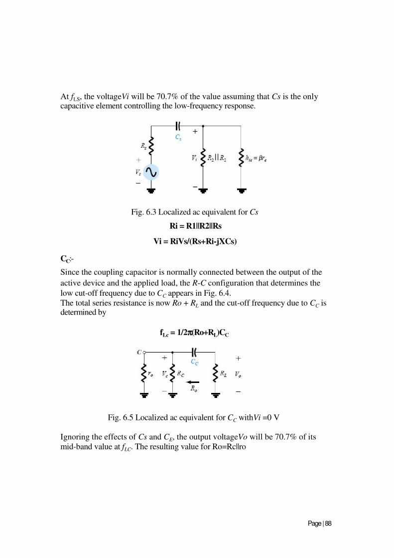
Anjuman-I-Islam’s Kalsekar Technical Campus, New Panvel
At fLS, the voltageVi will be 70.7% of the value assuming that Cs is the only capacitive element controlling the low-frequency response.
Fig. 6.3 Localized ac equivalent for Cs
Ri = R1||R2||Rs
Vi = RiVs/(Rs+Ri-jXCs)
CC:-
Since the coupling capacitor is normally connected between the output of the
active device and the applied load, the R-C configuration that determines the
low cut-off frequency due to CC appears in Fig. 6.4.
The total series resistance is now Ro + RL and the cut-off frequency due to CC is determined by
fLc = 1/2ππππ(Ro+RL)CC
Fig. 6.5 Localized ac equivalent for CC withVi =0 V
Ignoring the effects of Cs and CE, the output voltageVo will be 70.7% of its
mid-band value at fLC. The resulting value for Ro=Rc||ro
Page | 88
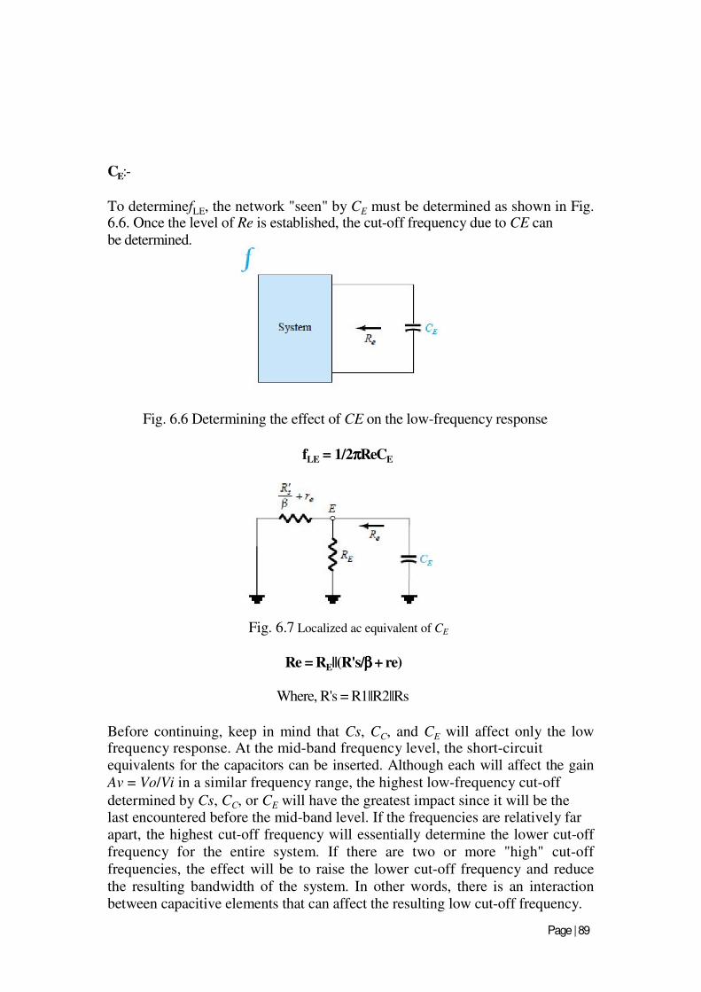
Anjuman-I-Islam’s Kalsekar Technical Campus, New Panvel
CE:-
To determinefLE, the network "seen" by CE must be determined as shown in Fig. 6.6. Once the level of Re is established, the cut-off frequency due to CE can
be determined.
Fig. 6.6 Determining the effect of CE on the low-frequency response
fLE = 1/2ππππReCE
Fig. 6.7 Localized ac equivalent of CE
Re = RE||(R's/ββββ + re)
Where, R's = R1||R2||Rs
Before continuing, keep in mind that Cs, CC, and CE will affect only the low frequency response. At the mid-band frequency level, the short-circuit equivalents for the capacitors can be inserted. Although each will affect the gain
Av = Vo/Vi in a similar frequency range, the highest low-frequency cut-off
determined by Cs, CC, or CE will have the greatest impact since it will be the last encountered before the mid-band level. If the frequencies are relatively far apart, the highest cut-off frequency will essentially determine the lower cut-off
frequency for the entire system. If there are two or more "high" cut-off
frequencies, the effect will be to raise the lower cut-off frequency and reduce
the resulting bandwidth of the system. In other words, there is an interaction
between capacitive elements that can affect the resulting low cut-off frequency.
Page | 89
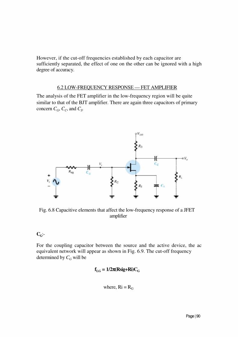
Anjuman-I-Islam’s Kalsekar Technical Campus, New Panvel
However, if the cut-off frequencies established by each capacitor are
sufficiently separated, the effect of one on the other can be ignored with a high
degree of accuracy.
6.2 LOW-FREQUENCY RESPONSE — FET AMPLIFIER
The analysis of the FET amplifier in the low-frequency region will be quite
similar to that of the BJT amplifier. There are again three capacitors of primary
concern CG, CC, and CS.
Fig. 6.8 Capacitive elements that affect the low-frequency response of a JFET
amplifier
CG:- For the coupling capacitor between the source and the active device, the ac
equivalent network will appear as shown in Fig. 6.9. The cut-off frequency
determined by CG will be
fLG = 1/2ππππ(Rsig+Ri)CG
where, Ri = RG
Page | 90
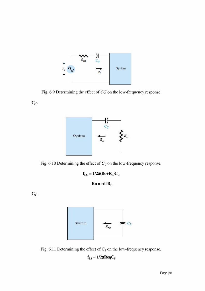
Anjuman-I-Islam’s Kalsekar Technical Campus, New Panvel
Fig. 6.9 Determining the effect of CG on the low-frequency response
CC:-
Fig. 6.10 Determining the effect of CC on the low-frequency response.
fLC = 1/2ππππ(Ro+RL)CC
Ro = rd||RD
CS:-
Fig. 6.11 Determining the effect of CS on the low-frequency response.
fLS = 1/2ππππReqCS
Page | 91
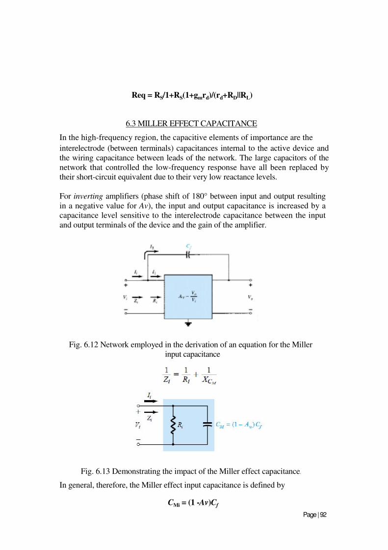
Anjuman-I-Islam’s Kalsekar Technical Campus, New Panvel
Req = RS/1+RS(1+gmrd)/(rd+RD||RL)
6.3 MILLER EFFECT CAPACITANCE
In the high-frequency region, the capacitive elements of importance are the
interelectrode (between terminals) capacitances internal to the active device and
the wiring capacitance between leads of the network. The large capacitors of the
network that controlled the low-frequency response have all been replaced by
their short-circuit equivalent due to their very low reactance levels.
For inverting amplifiers (phase shift of 180° between input and output resulting
in a negative value for Av), the input and output capacitance is increased by a
capacitance level sensitive to the interelectrode capacitance between the input
and output terminals of the device and the gain of the amplifier.
Fig. 6.12 Network employed in the derivation of an equation for the Miller
input capacitance
Fig. 6.13 Demonstrating the impact of the Miller effect capacitance.
In general, therefore, the Miller effect input capacitance is defined by
CMi = (1 -Av)Cf
Page | 92
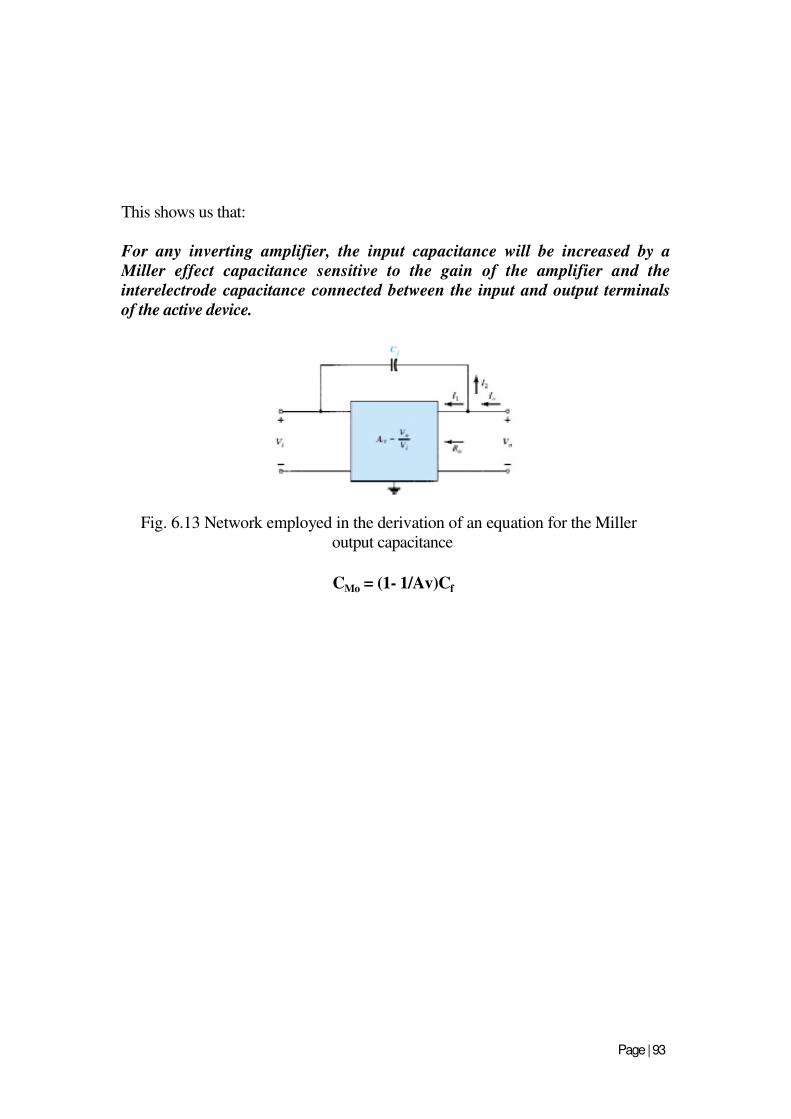
Anjuman-I-Islam’s Kalsekar Technical Campus, New Panvel
This shows us that:
For any inverting amplifier, the input capacitance will be increased by a
Miller effect capacitance sensitive to the gain of the amplifier and the
interelectrode capacitance connected between the input and output terminals
of the active device.
Fig. 6.13 Network employed in the derivation of an equation for the Miller
output capacitance
CMo = (1- 1/Av)Cf
Page | 93

Anjuman-I-Islam’s Kalsekar Technical Campus, New Panvel


