356
Government of Karnataka Department of Pre University Education ELECTRONICS Prescribed Textbook for I PUC
| Date post: | 22-Jan-2023 |
| Category: |
Documents |
| Upload: | khangminh22 |
| View: | 0 times |
| Download: | 0 times |
Government of Karnataka Department of Pre University Education
ELECTRONICS
Prescribed Textbook for I PUC
Revised Edition - 2017
Director’s Message Dear Students,
We at the Department of Pre-university Education,
Karnataka strive to empower each student to dream big
and equip them with the tools that enable them to reach
new heights and successfully deal with the challenges of
life. As Swami Vivekananda said, "Real education is that
which enables one to stand on one's own legs".
The course contents in this book are designed with
the objective of equipping you well for the next level of
study.
We wish you well on your journey and look forward to
you becoming a responsible citizen of the nation and give
back to the betterment of the society.
With best wishes,
Sd/- C. Shikha, IAS
Director Department of Pre University Education
Bengaluru


Textbook Development Committee
Shobhadevi Chair Person
Lecturer, Dept. of Electronics,
Vivekananda Pre-University College,
Dr Rajkumar road, Bangalore - 560 055.
Shivashankar K Coordinator-Chief Editor
Lecturer, Dept. of Electronics,
Govt PU College for Girls, Vani Vilas Institute, Fort,
Bangalore – 560 002.
Vanamala V Member-Assistant Editor
Lecturer, Dept. of Electronics,
Govt PU College for Girls, 13th cross, Malleswaram, Bangalore -12. [email protected]
Karani Umakanth Member,
Editorial Committee
Lecturer, Dept. of Electronics,
Govt PU College for Girls, Channapattana, Ramanagara District. [email protected]
Geeta R Shindhe
Member,
Editorial Committee
Lecturer, Dept. of Electronics,
BEL PU College, Jalahalli, Bengalore - 560013. [email protected]
Savitha R
Member, Editorial Committee
Lecturer, Dept. of Electronics,
Vidya Mandir Independent PU College, 11th Cross Malleswaram, Bangalore – 560 003. [email protected]
Deepti S Member, Editorial Committee
Lecturer, Dept. of Electronics,
Sri Jagadguru Renukacharya PU College, # 9, Race Course Road, Bangalore – 560009. [email protected]
Latamaheshwari KB Member
Lecturer, Dept. of Electronics,
Canara PU College, Mangalore – 03. [email protected]
Gopal Sagar
Member
Lecturer, Dept. of Electronics,
Govt Ex-Municiple PU College, Bellary. [email protected]
Subrahmanya KH
Member
Lecturer, Dept. of Electronics, Sri Marikamba Govt
PU College, Sirsi, Karwar District.
Umarani S
Member
Lecturer, Dept. of Electronics, SBRRS Mahajana
PU College, Jayalakshimipuram, Mysore –12.

Pawar Chandu V
Member
Lecturer, Dept. of Electronics,
Govt PU College for Boys, Nanjangudu, Mysore District. [email protected]
Nagaraj K
Member
Lecturer, Dept. of Electronics,
Govt PU College, Theertha Halli, Shimoga District. [email protected]
Nizamoddin Shebeersab
Member
Lecturer, Dept. of Electronics,
Govt Sardar PU College, Belgaum – 590 002. [email protected]
Malleswara M
Member
Lecturer, Dept. of Electronics,
Nutana Vidyalaya PU College, Gulbarga. [email protected]
Kotragouda K
Member
Lecturer, Dept. of Electronics,
M E S PU college, B T M Layout, Bangalore - 560 076. [email protected]
Shivaraj R
Member
Lecturer, Dept. of Electronics,
Govt PU college, Nagamangala, Mandya District. [email protected]
Latha KR
Member
Lecturer, Dept. of Electronics,
Shree Siddaganga PU college for Women, Tumkur. [email protected]
Shivakumar K
Member
Lecturer, Dept. of Electronics,
Govt PU college [M.P.H.S], Super Market, Gulbarga - 01. [email protected]
Shashidar TM
Member
Lecturer, Dept. of Electronics,
Reva PU college, Yelahanka, Bangalore. [email protected]
Smitha Paul Reviewer
Lecturer, Dept. of Electronics,
Mount Carmel PU College, Palace Road, Vasanth Nagar, Bangalore - 52. [email protected]
Sudha G
Reviewer
Lecturer, Dept. of Electronics,
Marimallappa PU College, Mysore. [email protected]
Anupama
Reviewer
Lecturer, Dept. of Electronics, Sheshadripuram Independent PU College, Bangalore. [email protected]
ACKNOWLEDGEMENT
The Dept. of Pre-University Education acknowledges the valuable contribution
of the individuals and organizations involved in the development of Electronics
Textbook for I PUC.
The Dept. of Pre-University Education gratefully acknowledges Sri.
Chakravarthi Mohan, Director, for his support and guidance in preparing the
Textbook.
The Dept. of Pre-University Education acknowledges Smt. N Rohini, Joint
Director, for her consistent efforts in bringing out syllabus and Textbook.
The Dept. of Pre-University Education also acknowledges Sri. Dr M N Katti and
Sri. Mahesh B, section officers, for their endless service in bringing out the
Textbook.
The Dept. of Pre-University Education acknowledges CET CELL authorities for
providing the venue for the succeeding discussions on the syllabus and the
Textbook.
The Dept. of Pre-University Education acknowledges Smt. Florence Rita Rao,
Principal and Sri. Shivaprakash N V, Administrative Manager, Bharat
Electronics Limited’s BEL PU College, Jalahalli, Bangalore for providing the
venue to conduct the workshop related to the Textbook.
The Dept. of Pre-University Education acknowledges Smt. Shobha N C,
Principal, Govt. PU College for Girls, Malleswaram, Bangalore, for providing the
computer section to prepare the draft copy of the Textbook.
The Dept. of Pre-University Education acknowledges Smt. Asha Srinivas,
Principal, Govt. PU College for Girls, Vani Vilas Institute, Fort, Bangalore-02,
for providing the facility to edit and review the Textbook.
The Dept. of Pre-University Education acknowledges Sri Sudhakar Hegde,
Selection Grade Lecturer, Dept. of Electronics, Vijaya PU College, 4th Block
Jayanagar, Bangalore and Smt. Shruthi V Kustagi, Lecturer, Dept. of
Electronics, PES PU College, Hanumanthanagar, Bangalore for their work in
fine-tuning the Textbook.
The Dept also acknowledges Sri. Beeresh B P, Lecturer, Dept. of Electronics,
New Horizon PU College, Bangalore for his help in preparing a draft copy on
Introduction to Electronics.
It is a pleasure to thank Sri. Nagaraj P, Computer Instructor, Govt. PU College
for Girls, Malleswaram, Sri. Govindaraju, Lecturer, Dept. of Electronics, Sri.
Sujankumar M V, Technical drawings draftsman and Sri. Venkatesh K C, Lab
assistant of BEL PU College for their help in this work.
The contribution of the Publication Department in bringing out this book is
also duly acknowledged.
PREFACE
ELECTRONICS has been introduced for pre-university students of KARNATAKA
in the year 1986-87. In PUC, as a part of Science stream, PCME combination
was introduced as an option.
Fundamental foundation must be made available for the present generation, as
they are being brought up in an environment of modern technology.
The present world stands on the strong foundation of science creating
awareness in students towards technological advancements. We must impart
education based on their needs to create interest towards electronics.
This system of education demands for the syllabus to be framed in par with the
CBSC/ICSE/ISC, as these streams mainly deals with basics of science,
technology and research. Keeping all these in view we have framed the theory
syllabus to 120 hours.
This book is the result of renewed efforts of the present Textbook Development
Committee with the hope that the students will appreciate the beauty and logic
of electronics.
For students pursuing electronics as the subject in their further studies the
matter developed in this book will certainly provide sound base.
For students, to grab and understand concepts book is written in a simple but
systematic way. Chapter name, text material, questions based on
understanding, knowledge, skill, applications and exercises has been
introduced in an organized manner.
Among the nine chapters, the first seven chapters are categorized under analog
electronics, chapter 8 under digital electronics and chapter 9 introduces
practical electronic components utilized in circuits. Chapter 1 gives an
interesting insight on the everlasting electronics in various fields. Chapter 2
focuses on various concepts of charge, laws and theorems to analyse the
electrical networks. Also gives a brief idea of AC principles. Chapter 3 provides
awareness of using measuring instruments related to electrical, electronics and
medical fields. Chapter 4 gives in-depth knowledge about passive electronic
components and transducers. Chapter 5 provides the knowledge of using AC
and DC to the passive components. Chapter 6 gives the clear concepts related
to semiconductor devices and its application towards regulated power supply
and also about display units. Chapter 7 introduces a brief idea on working and

configurations of a current controlled device BJT. Chapter 8 enlightens on
number systems, Boolean law’s, human logical ideas implemented as gates and
applications of timer. Chapter 9 gives a clear idea on electronic components to
design and develop the practical electronic circuits.
In writing this book our greatest inspiration is OUR STUDENTS in KARNATAKA
STATE, INDIA. Our humble and heartfelt gratitude to all our friends of
Karnataka state who have inspired and assisted our team in this venture.
The final supreme judges are our READERS.
Readers are welcome to share their esteemed thoughts and valuable
suggestions in improving the Textbook.
Send your feedback to [email protected]
SHOBHA DEVI
CHAIR PERSON
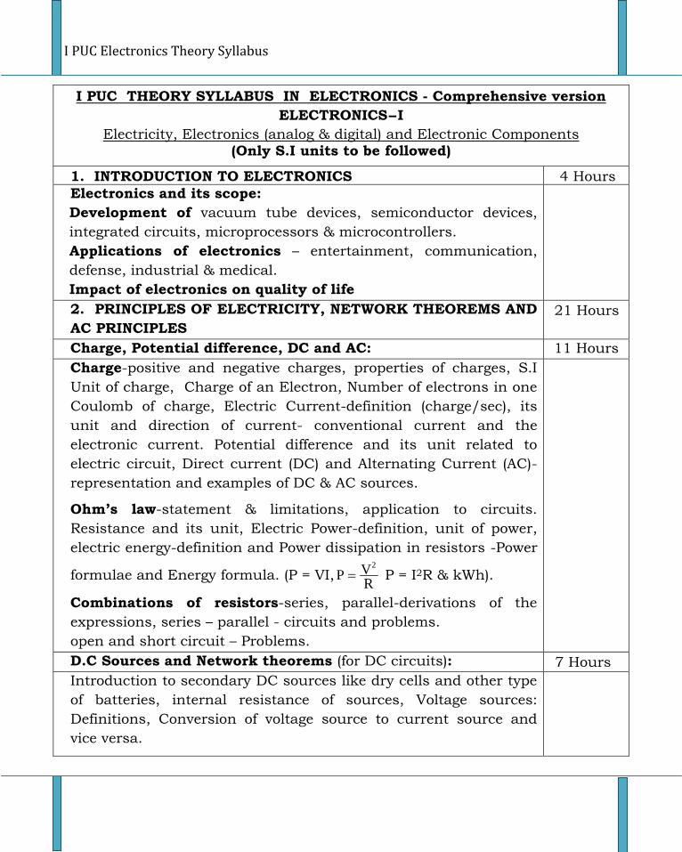
I PUC Electronics Theory Syllabus
I PUC THEORY SYLLABUS IN ELECTRONICS - Comprehensive version
ELECTRONICS-I
Electricity, Electronics (analog & digital) and Electronic Components (Only S.I units to be followed)
1. INTRODUCTION TO ELECTRONICS 4 Hours
Electronics and its scope:
Development of vacuum tube devices, semiconductor devices,
integrated circuits, microprocessors & microcontrollers.
Applications of electronics – entertainment, communication,
defense, industrial & medical.
Impact of electronics on quality of life
2. PRINCIPLES OF ELECTRICITY, NETWORK THEOREMS AND
AC PRINCIPLES
21 Hours
Charge, Potential difference, DC and AC: 11 Hours
Charge-positive and negative charges, properties of charges, S.I
Unit of charge, Charge of an Electron, Number of electrons in one
Coulomb of charge, Electric Current-definition (charge/sec), its
unit and direction of current- conventional current and the
electronic current. Potential difference and its unit related to
electric circuit, Direct current (DC) and Alternating Current (AC)-
representation and examples of DC & AC sources.
Ohm’s law-statement & limitations, application to circuits.
Resistance and its unit, Electric Power-definition, unit of power,
electric energy-definition and Power dissipation in resistors -Power
formulae and Energy formula. (P = VI,RVP
2
P = I2R & kWh).
Combinations of resistors-series, parallel-derivations of the
expressions, series – parallel - circuits and problems.
open and short circuit – Problems.
D.C Sources and Network theorems (for DC circuits): 7 Hours
Introduction to secondary DC sources like dry cells and other type
of batteries, internal resistance of sources, Voltage sources:
Definitions, Conversion of voltage source to current source and
vice versa.
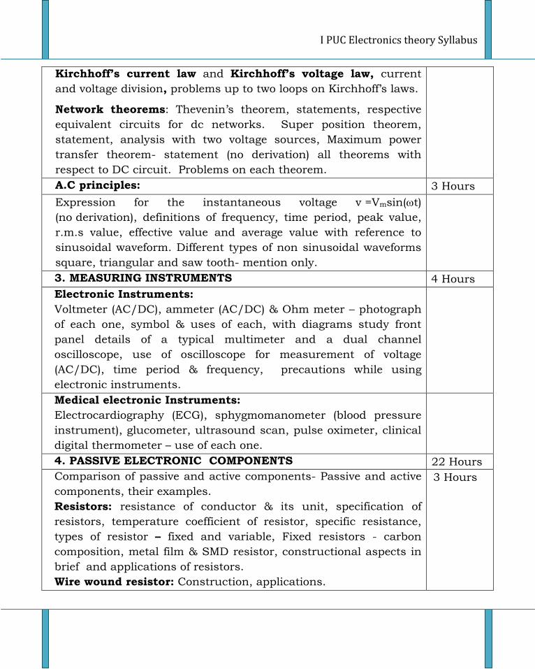
I PUC Electronics theory Syllabus
Kirchhoff’s current law and Kirchhoff’s voltage law, current
and voltage division, problems up to two loops on Kirchhoff’s laws.
Network theorems: Thevenin’s theorem, statements, respective
equivalent circuits for dc networks. Super position theorem,
statement, analysis with two voltage sources, Maximum power
transfer theorem- statement (no derivation) all theorems with
respect to DC circuit. Problems on each theorem.
A.C principles: 3 Hours
Expression for the instantaneous voltage v =Vmsin(t)
(no derivation), definitions of frequency, time period, peak value,
r.m.s value, effective value and average value with reference to
sinusoidal waveform. Different types of non sinusoidal waveforms
square, triangular and saw tooth- mention only.
3. MEASURING INSTRUMENTS 4 Hours
Electronic Instruments:
Voltmeter (AC/DC), ammeter (AC/DC) & Ohm meter – photograph
of each one, symbol & uses of each, with diagrams study front
panel details of a typical multimeter and a dual channel
oscilloscope, use of oscilloscope for measurement of voltage
(AC/DC), time period & frequency, precautions while using
electronic instruments.
Medical electronic Instruments:
Electrocardiography (ECG), sphygmomanometer (blood pressure
instrument), glucometer, ultrasound scan, pulse oximeter, clinical
digital thermometer – use of each one.
4. PASSIVE ELECTRONIC COMPONENTS 22 Hours
Comparison of passive and active components- Passive and active
components, their examples.
Resistors: resistance of conductor & its unit, specification of
resistors, temperature coefficient of resistor, specific resistance,
types of resistor – fixed and variable, Fixed resistors - carbon
composition, metal film & SMD resistor, constructional aspects in
brief and applications of resistors.
Wire wound resistor: Construction, applications.
3 Hours
I PUC Electronics Theory Syllabus
Variable resistors: Potentiometer – carbon composition type -
construction and uses, Preset.
Importance of power rating in resistors.
Color coding of resistors (4 bands & 5 bands), tolerance, and
problems.
Capacitors: 6 Hours
Definition of Capacitance and its unit - Principle of capacitor,
factors affecting the capacitance of capacitor, parallel plate
capacitor (mention C = oA/d and C = orA/d-no derivation), energy
stored in a capacitor E = ½CV2 (no derivation), dielectric and
examples, role of dielectric in capacitor.
Types of Capacitors – fixed and variable.
Fixed capacitors: Ceramic, Polystyrene, SMD capacitor and
Electrolytic capacitor - construction and applications. variable
capacitors like ganged capacitor and trimmer - their applications
Importance of voltage rating in capacitors.
Capacitive networks - derivation of expressions for effective
capacitance of capacitors connected in series or in parallel trouble
shooting in capacitors - open short, leakage.
Inductors: 10 Hours
Review of laws of electromagnetic Induction
Definitions of self, mutual inductances and unit of Inductance.
Inductor - factors determining the inductance of inductor
AμNL
2
Energy stored in an inductor i.e., E = ½ LI2 (no derivation), Fixed Inductors: Air core, iron core, ferrite core - construction and
applications.
Expressions for series and parallel combination of inductors
neglecting the mutual inductance (no derivations), choke and
relays.
Transformers: Principle (mutual induction), Turns ratio, voltage
ratio and current ratio - relation between them, step up and step
down transformers, Centre tapping in transformers, problems,
applications of transformers, Efficiency in transformers, AF & IF
I PUC Electronics theory Syllabus
transformers, pulse transformer.
Transducers: 3 Hours
Definition of transducer, pressure transducers - microphone and
loud speaker - construction, working and applications,
Temperature transducers [Thermistor-Negative Temperature
Coefficient (NTC) and Positive Temperature Coefficient (PTC) - only
mention], LM 35 temperature sensor, LDR, Applications of
temperature transducer.
5. APPLICATION OF D.C AND A.C TO PASSIVE COMPONENTS 14 Hours
D.C applied to Passive components: 2 Hours
Transient phenomenon, transient period, Charging & discharging of
a capacitor in RC circuit - expressions (mention only-no
derivations), definition of Time constant, graphical representations
for charging & discharging of a capacitor. Growth and decay of
current in RL circuit - expressions (no derivations), definition for
Time constant, graphical representations for growth and decay of
current. Problems on RC & RL circuits.
A.C applied to Passive components: 12 Hours
Concept of phase and phase difference.
AC applied to resistive circuit: Phasor representation of voltage
and current waveforms.
AC applied to capacitive circuit: Circuit diagram, Expression for
instantaneous current and voltage for a sinusoidal input voltage,
Phasor representation of voltage and current, definition of phase,
phase difference - Lead and lag concepts.
AC applied to inductive circuit: Circuit diagram, Expression for
instantaneous current and voltage for a sinusoidal input voltage,
Phasor representation of voltage and current, definition of
phase, phase difference - Lead and lag concepts.
Resistance, reactance and impedance. Capacitive reactance and
inductive reactance-definitions and expressions.
Power in AC circuit: Power factor, active and reactive power.
Series RLC circuits: Impedance, impedance equation (mention
I PUC Electronics Theory Syllabus
only), variation of impedance with respect to frequency.
Series Resonance - Condition for resonance, Resonant frequency,
Half power frequencies, BW, Quality factor in terms of fr & BW.
Frequency & phase response of RC circuits: Brief note on filters
and its application. Low pass and high pass filters - frequency
response and phase response graph and Cutoff frequency,
problems.
6. SEMICONDUCTORS, DIODES AND APPLICATIONS OF
DIODES
26 Hours
Semiconductor theory: 4 Hours
Band theory of solids - valence band, conduction band and the
forbidden energy gap, Classification of solids as conductors,
semiconductors and insulators on the basis of their conductivity
and on the basis of energy band diagrams, examples for each.
Types of semiconductors - Intrinsic and Extrinsic.
Intrinsic semiconductors: Definition, lattice structure (two
dimensional), concept of holes and electrons (their generation and
flow in the bands), effect of temperature, thermal generation and
recombination of electrons and holes.
Extrinsic semiconductors: Definition, doping, doping elements -
trivalent and pentavalent, meaning of donor and acceptor
impurities.
Types of Extrinsic Semiconductors: n type and p type, their
formation, in each case study of lattice structure (two dimensional).
pn junction: 4 Hours
Formation of pn junction, diffusion of charge carriers, depletion
region - formation of depletion region, barrier width and barrier
potential, semiconductor diode.
Forward biased pn junction: Diagram, Effect on width of the
depletion region, resistance and current flow.
Reverse biased pn junction: Diagram, Effect on width of the
depletion region, resistance and concept of leakage current (in
germanium and silicon), junction capacitance (during reverse bias)
I PUC Electronics theory Syllabus
and its variation with applied reverse bias voltage, brief note on
breakdown mechanisms.
Junction Diode 8 Hours
Circuit symbol, Diode equation
)1(II TV
V
eO
- Numerical problems
need not be discussed. Ideal and practical diodes, Equivalent circuit
of a practical diode (barrier potential in series with Rf).
V-I static characteristics - Circuits to study the forward bias and
reverse bias characteristics, characteristic curves, knee voltage,
forward bias resistance from characteristic curve. Study of various
terms related to diode like PIV and power rating (qualitative), diode
approximations, Comparison of Germanium and Silicon diodes.
Wave shaping circuits – clippers – series positive clippers, series
negative clippers, clampers - positive clampers, negative clampers.
Rectification – Need for rectification, Principles, Half wave rectifier,
Full wave rectifier (centre tapped and bridge type): Circuit, working
of rectifiers considering transformers at the input, input and output
wave forms for the rectifiers. Expression for Load regulation -
mention only. Expressions (no derivations) for average output
voltage Vav, average output current Iav, Vrms and Irms. Efficiency ‘’
(expression - no derivation), Ripple and Ripple factor (expression-
no derivation) for each case, comparison of rectifiers. Concept of
negative voltage rectifiers. Problems.
Filters: 2 Hours
Need for filters, series inductor filter, shunt capacitor filter and
Inductive input L type filter, - circuit diagram, working and
waveforms for each type, bleeder resistance.
Special purpose diodes & voltage regulators: 8 Hours
Zener diode: schematic symbol, Zener and avalanche breakdown,
V-I characteristics of Zener diode, its application in voltage
regulation-study of line and load regulation, Calculation of
minimum load resistance required for regulation - problems with
constant input & variable input voltage.
I PUC Electronics Theory Syllabus
Design of practical regulated power supplies – Design of a
rectifier for a given DC voltage, Fixed positive regulated power
supply using 7812, Fixed negative regulated power supply using
7912 & Adjustable regulated power supply using LM317.
Specifications of DC regulated power supply.
Light Emitting Diode (LED) - symbol, construction - type of
materials used, working in brief and applications. Varactor diode, IR
emitter diode, photo diode, tunnel diode & Schottkey diode -
symbol, and applications.
Seven segment display: LED display - pin configuration showing the
different segments-a, b, c, d, e, f, g and dp. Common Anode and
Common Cathode display. Display of digits 0 to 9, use of current
limiting resistors for each segment, applications. LCD (Liquid
Crystal Display), Comparison of L.E.D displays with L.C.D displays.
7. BIPOLAR JUNCTION TRANSISTOR 7 Hours
Transistor working-npn (in active mode), Symbols, currents IB, IC
and IE, Three basic configurations of transistor – CE, CB and CC.
DC current gains and β and the relationship between them. Input
and output characteristics of a transistor in CE configuration.
Meaning of cutoff, saturation, and active regions.
Photo transistor, Opto-coupler & IR receiver transistor – working in
brief, symbol & applications
8. INTRODUCTION TO DIGITAL ELECTRONICS 18 Hours
Introduction, importance of Digital Electronics, representation of
digital and Binary signals, Positive and Negative logic.
Number systems – Need for the study of various number systems,
Decimal number system, and Binary number system – advantage,
bit, nibble, byte, memory representation using Bytes, hexadecimal
number systems, conversion from one system to another. Binary
addition, subtraction, multiplication and division, 1’s complement,
2’s complement, 1’s complement and 2’s complement method for
subtraction of binary numbers (subtraction of a binary number of
smaller value from a number of larger value), sign magnitude binary
number.
I PUC Electronics theory Syllabus
Boolean algebra and Logic gates:
Boolean Algebra: Introduction to Boolean Algebra, Basic Boolean
operators (OR, AND and NOT operators), Basic Laws and theorems
of Boolean Algebra, De Morgan's theorems and their verification,
Boolean identities, Simplification of Boolean expressions,
Basic Logic gates: OR gate and AND gate: Logic symbol, truth table
and realization using diodes, NOT gate - using transistor, logic
symbol and truth table. (Positive logic is to be dealt in all cases).
Construction of logic circuits for logic expressions.
DTL - NAND, DTL - NOR gates – working and truth table.
Pulse (clock) generator using 555 - Astable multivibrator -
frequency & duty cycle, monostable pulse generator – pulse width.
9. PRACTICAL ELECTRONIC COMPONENTS, THEIR
SPECIFICATIONS AND PCB
[Note: photographs, important specifications, part numbers
(wherever possible) of each component to be mentioned]
Components part numbers, data sheet, package
Resistors – CFR, MFR, SMD resistor, wire wound resistor, fusible
Resistor.
Potentiometer & trimmer resistors
Capacitors – Mica, ceramic, polystyrene, electrolytic, SMD
capacitor, trimmer capacitor
Inductors – air core, iron core, ferrite core
Electromagnetic relay
Transformers – Iron core, ferrite core
Diodes – rectifying diodes, diode bridge module, switching diodes,
Zener diode, LEDs, seven segment display, LCD display.
Transistors – npn & pnp transistors
Sensors: speaker, microphone, temperature sensor, thermistor,
LDR, IR emitter diode, IR receiver transistor
Regulators- Fixed regulator: 78XX series, 79XX series,
PCB Design & development
4 Hours
Note: Numerical Problems are to be solved for all the expressions
wherever appear in the syllabus.
***** sds
*****
Contents
Page
1. Introduction to electronics 1
2. Principles of electricity, Network theorems and AC principles 15
3. Measuring instruments 85
4. Passive electronic components 99
5. Application of DC and AC to passive components 163
6. Semiconductors, diodes and applications of diodes 187
7. Bipolar junction transistor 267
8. Introduction to digital electronics 281
9. Practical electronic components, their specifications and PCB 321

Ch 1: Introduction to Electronics
Page 1
Chapter 1
Introduction to Electronics
Electronics and its Scope
The word ‘electronics’ is derived from electron mechanics. Electronics is the
science and technology of the motion of electrons in gas, vacuum, or in
semiconductor devices which serves as a base for electrical signals thereon. An
Electrical signal may represent information by the voltage, current, frequency,
or total charge. The Institute of Radio Engineers has given a definition of
electronics as "the field of science and engineering, which deals with
electron devices and their utilization." Experiments with beams of negative
particles were performed by Joseph John ("J.J.") Thomson, which led to the
conclusion in 1897 that they consisted of light weight particles with a negative
electric charge, nowadays known as electrons. Electronics can be broadly
divided into Analog and Digital Electronics. In Analog electronics, electronic
systems with a continuously variable signal, in contrast to digital electronics
where signals usually take only two different levels.
Electronics deals principally with the communication of information and/or
data handling. Until around 1960, electronics was considered as an integral
part of electrical engineering. But due to the tremendous advancement over the
last few decades, electronics has now gained its rightful place. The
advancement has been so fast that many sub-branches of electronics such as
Computer Science Engineering, Communication Engineering, Control and
Instrumentation Engineering, Information Technology are now full-fledged
courses in many universities. Everyone is familiar with electronics, be it the
television, the computer, internet or the cellular phone. An Electronics
Engineer knows and understands the functioning of these devices. He acquires
the capability to further improvise these devices as per the needs of the user.
Electronic engineering technicians have opportunities in installation, operation
and maintenance of electronic equipments and systems. Defence, space and
other large research organisations employ electronic engineers in design and
development of complex devices and systems for signal processing and
I PUC Electronics
Page 2
telecommunication. Industries involved in design and fabrication of the
devices, integrated circuits, embedded systems, electronic equipments etc have
also provided large scale placements for engineers with this specialisation.
Installation and maintenance of electronic equipments used for health care in
hospitals, equipments and systems for instrumentation and control in process
industries, automation systems of assembly line in production industries, etc
are also handled by electronics technicians.
Knowledge of computer hardware, networking equipments and communication
systems enabled electronics engineering graduates to annexe an edge in the IT
job market. The skills and understanding developed in the course enables them
to be preferred, as software professionals by IT.
Development of Electronics
Vacuum tube devices
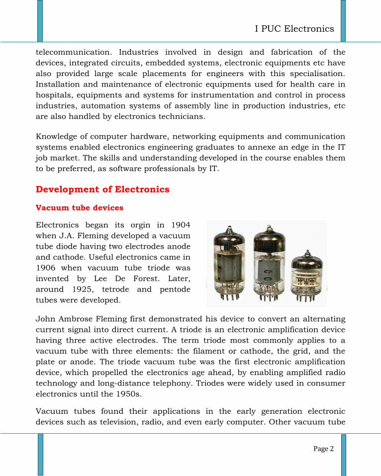
Electronics began its orgin in 1904
when J.A. Fleming developed a vacuum
tube diode having two electrodes anode
and cathode. Useful electronics came in
1906 when vacuum tube triode was
invented by Lee De Forest. Later,
around 1925, tetrode and pentode
tubes were developed.
John Ambrose Fleming first demonstrated his device to convert an alternating
current signal into direct current. A triode is an electronic amplification device
having three active electrodes. The term triode most commonly applies to a
vacuum tube with three elements: the filament or cathode, the grid, and the
plate or anode. The triode vacuum tube was the first electronic amplification
device, which propelled the electronics age ahead, by enabling amplified radio
technology and long-distance telephony. Triodes were widely used in consumer
electronics until the 1950s.
Vacuum tubes found their applications in the early generation electronic
devices such as television, radio, and even early computer. Other vacuum tube
Ch 1: Introduction to Electronics
Page 3
devices include the X-Ray Tubes, Cathode Ray Tubes and Magnetrons.
Vacuum tubes are also used in television screens and computer monitor screen
- even as we speak now they have been replaced by LCD/LED screens.
Semiconductor devices
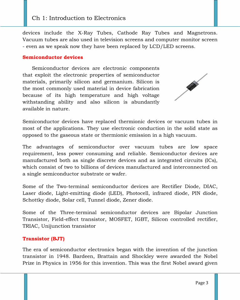
Semiconductor devices are electronic components
that exploit the electronic properties of semiconductor
materials, primarily silicon and germanium. Silicon is
the most commonly used material in device fabrication
because of its high temperature and high voltage
withstanding ability and also silicon is abundantly
available in nature.
Semiconductor devices have replaced thermionic devices or vacuum tubes in
most of the applications. They use electronic conduction in the solid state as
opposed to the gaseous state or thermionic emission in a high vacuum.
The advantages of semiconductor over vacuum tubes are low space
requirement, less power consuming and reliable. Semiconductor devices are
manufactured both as single discrete devices and as integrated circuits (ICs),
which consist of two to billions of devices manufactured and interconnected on
a single semiconductor substrate or wafer.
Some of the Two-terminal semiconductor devices are Rectifier Diode, DIAC,
Laser diode, Light-emitting diode (LED), Photocell, infrared diode, PIN diode,
Schottky diode, Solar cell, Tunnel diode, Zener diode.
Some of the Three-terminal semiconductor devices are Bipolar Junction
Transistor, Field-effect transistor, MOSFET, IGBT, Silicon controlled rectifier,
TRIAC, Unijunction transistor
Transistor (BJT)
The era of semiconductor electronics began with the invention of the junction
transistor in 1948. Bardeen, Brattain and Shockley were awarded the Nobel
Prize in Physics in 1956 for this invention. This was the first Nobel award given
I PUC Electronics
Page 4
for an engineering device in nearly 50 years. Soon transistors were replacing
the bulky vacuum tubes in different electronic circuits.
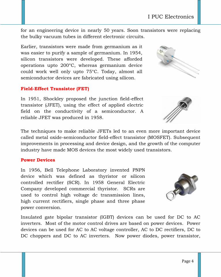
Earlier, transistors were made from germanium as it
was easier to purify a sample of germanium. In 1954,
silicon transistors were developed. These afforded
operations upto 200°C, whereas germanium device
could work well only upto 75°C. Today, almost all
semiconductor devices are fabricated using silicon.
Field-Effect Transistor (FET)
In 1951, Shockley proposed the junction field-effect
transistor (JFET), using the effect of applied electric
field on the conductivity of a semiconductor. A
reliable JFET was produced in 1958.
The techniques to make reliable JFETs led to an even more important device
called metal oxide-semiconductor field-effect transistor (MOSFET). Subsequent
improvements in processing and device design, and the growth of the computer
industry have made MOS devices the most widely used transistors.
Power Devices
In 1956, Bell Telephone Laboratory invented PNPN
device which was defined as thyristor or silicon
controlled rectifier (SCR). In 1958 General Electric
Company developed commercial thyristor. SCRs are
used to control high voltage dc transmission lines,
high current rectifiers, single phase and three phase
power conversion.
Insulated gate bipolar transistor (IGBT) devices can be used for DC to AC
inverters. Most of the motor control drives are based on power devices. Power
devices can be used for AC to AC voltage controller, AC to DC rectifiers, DC to
DC choppers and DC to AC inverters. Now power diodes, power transistor,
Ch 1: Introduction to Electronics
Page 5
SCRs, TRIACs, MOSFETs, and IGBTs are available with voltage rating of
several thousand volts and current rating up to several thousand amps.
Integrated circuits
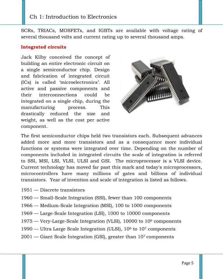
Jack Kilby conceived the concept of
building an entire electronic circuit on
a single semiconductor chip. Design
and fabrication of integrated circuit
(ICs) is called ‘microelectronics’. All
active and passive components and
their interconnections could be
integrated on a single chip, during the
manufacturing process. This
drastically reduced the size and
weight, as well as the cost per active
component.
The first semiconductor chips held two transistors each. Subsequent advances
added more and more transistors and as a consequence more individual
functions or systems were integrated over time. Depending on the number of
components included in integrated circuits the scale of integration is referred
to SSI, MSI, LSI, VLSI, ULSI and GSI. The microprocessor is a VLSI device.
Current technology has moved far past this mark and today's microprocessors,
microcontrollers have many millions of gates and billions of individual
transistors. Year of invention and scale of integration is listed as follows.
1951 — Discrete transistors
1960 — Small-Scale Integration (SSI), fewer than 100 components
1966 — Medium-Scale Integration (MSI), 100 to 1000 components
1969 — Large-Scale Integration (LSI), 1000 to 10000 components
1975 — Very-Large-Scale Integration (VLSI), 10000 to 106 components
1990 — Ultra Large Scale Integration (ULSI), 106 to 107 components
2001 — Giant Scale Integration (GSI), greater than 107 components
I PUC Electronics
Page 6
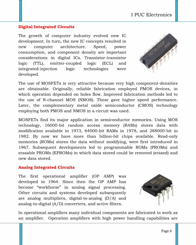
Digital Integrated Circuits
The growth of computer industry evolved new IC
development. In turn, the new IC concepts resulted in
new computer architecture. Speed, power
consumption, and component density are important
considerations in digital ICs. Transistor-transistor
logic (TTL), emitter-coupled logic (ECL) and
integrated-injection logic technologies were
developed.
The use of MOSFETs is very attractive because very high component-densities
are obtainable. Originally, reliable fabrication employed PMOS devices, in
which operation depended on holes flow. Improved fabrication methods led to
the use of N-channel MOS (NMOS). These gave higher speed performance.
Later, the complementary metal oxide semiconductor (CMOS) technology
employing both PMOS and NMOS in a circuit was used.
MOSFETs find its major application in semiconductor memories. Using MOS
technology, 16000-bit random access memory (RAMs) stores data with
modification available in 1973, 64000-bit RAMs in 1978, and 288000-bit in
1982. By now we have more than billion-bit chips available. Read-only
memories (ROMs) stores the data without modifying, were first introduced in
1967. Subsequent developments led to programmable ROMs (PROMs) and
erasable PROMs (EPROMs) in which data stored could be removed (erased) and
new data stored.
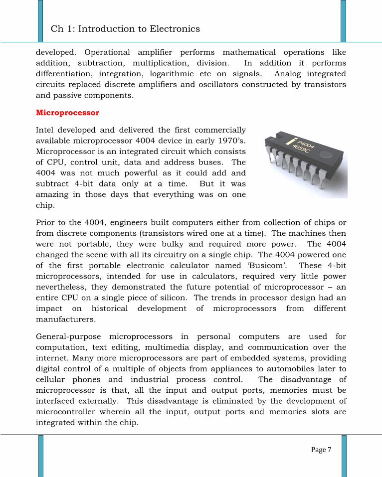
Analog Integrated Circuits
The first operational amplifier (OP AMP) was
developed in 1964. Since then the OP AMP has
become “workhorse” in analog signal processing.
Other circuits and systems developed subsequently
are analog multipliers, digital-to-analog (D/A) and
analog-to-digital (A/D) converters, and active filters.
In operational amplifiers many individual components are fabricated to work as
an amplifier. Operation amplifiers with high power handling capabilities are
Ch 1: Introduction to Electronics
Page 7
developed. Operational amplifier performs mathematical operations like
addition, subtraction, multiplication, division. In addition it performs
differentiation, integration, logarithmic etc on signals. Analog integrated
circuits replaced discrete amplifiers and oscillators constructed by transistors
and passive components.
Microprocessor
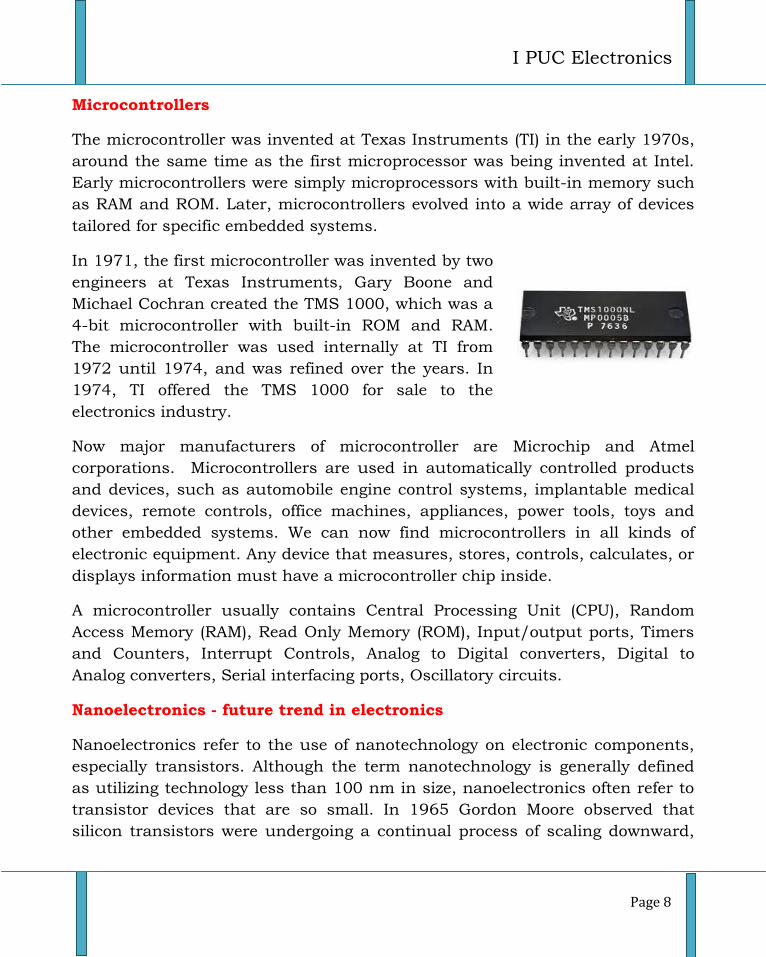
Intel developed and delivered the first commercially
available microprocessor 4004 device in early 1970’s.
Microprocessor is an integrated circuit which consists
of CPU, control unit, data and address buses. The
4004 was not much powerful as it could add and
subtract 4-bit data only at a time. But it was
amazing in those days that everything was on one
chip.
Prior to the 4004, engineers built computers either from collection of chips or
from discrete components (transistors wired one at a time). The machines then
were not portable, they were bulky and required more power. The 4004
changed the scene with all its circuitry on a single chip. The 4004 powered one
of the first portable electronic calculator named ‘Busicom’. These 4-bit
microprocessors, intended for use in calculators, required very little power
nevertheless, they demonstrated the future potential of microprocessor – an
entire CPU on a single piece of silicon. The trends in processor design had an
impact on historical development of microprocessors from different
manufacturers.
General-purpose microprocessors in personal computers are used for
computation, text editing, multimedia display, and communication over the
internet. Many more microprocessors are part of embedded systems, providing
digital control of a multiple of objects from appliances to automobiles later to
cellular phones and industrial process control. The disadvantage of
microprocessor is that, all the input and output ports, memories must be
interfaced externally. This disadvantage is eliminated by the development of
microcontroller wherein all the input, output ports and memories slots are
integrated within the chip.
I PUC Electronics
Page 8
Microcontrollers
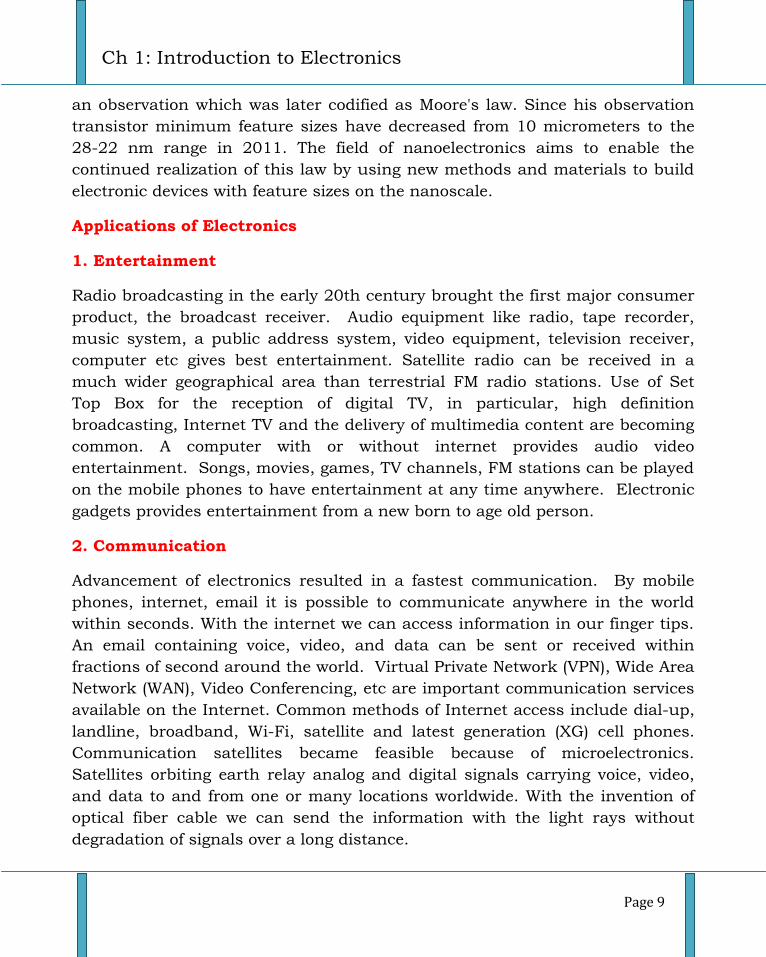
The microcontroller was invented at Texas Instruments (TI) in the early 1970s,
around the same time as the first microprocessor was being invented at Intel.
Early microcontrollers were simply microprocessors with built-in memory such
as RAM and ROM. Later, microcontrollers evolved into a wide array of devices
tailored for specific embedded systems.
In 1971, the first microcontroller was invented by two
engineers at Texas Instruments, Gary Boone and
Michael Cochran created the TMS 1000, which was a
4-bit microcontroller with built-in ROM and RAM.
The microcontroller was used internally at TI from
1972 until 1974, and was refined over the years. In
1974, TI offered the TMS 1000 for sale to the
electronics industry.
Now major manufacturers of microcontroller are Microchip and Atmel
corporations. Microcontrollers are used in automatically controlled products
and devices, such as automobile engine control systems, implantable medical
devices, remote controls, office machines, appliances, power tools, toys and
other embedded systems. We can now find microcontrollers in all kinds of
electronic equipment. Any device that measures, stores, controls, calculates, or
displays information must have a microcontroller chip inside.
A microcontroller usually contains Central Processing Unit (CPU), Random
Access Memory (RAM), Read Only Memory (ROM), Input/output ports, Timers
and Counters, Interrupt Controls, Analog to Digital converters, Digital to
Analog converters, Serial interfacing ports, Oscillatory circuits.
Nanoelectronics - future trend in electronics
Nanoelectronics refer to the use of nanotechnology on electronic components,
especially transistors. Although the term nanotechnology is generally defined
as utilizing technology less than 100 nm in size, nanoelectronics often refer to
transistor devices that are so small. In 1965 Gordon Moore observed that
silicon transistors were undergoing a continual process of scaling downward,
Ch 1: Introduction to Electronics
Page 9
an observation which was later codified as Moore's law. Since his observation
transistor minimum feature sizes have decreased from 10 micrometers to the
28-22 nm range in 2011. The field of nanoelectronics aims to enable the
continued realization of this law by using new methods and materials to build
electronic devices with feature sizes on the nanoscale.
Applications of Electronics
1. Entertainment
Radio broadcasting in the early 20th century brought the first major consumer
product, the broadcast receiver. Audio equipment like radio, tape recorder,
music system, a public address system, video equipment, television receiver,
computer etc gives best entertainment. Satellite radio can be received in a
much wider geographical area than terrestrial FM radio stations. Use of Set
Top Box for the reception of digital TV, in particular, high definition
broadcasting, Internet TV and the delivery of multimedia content are becoming
common. A computer with or without internet provides audio video
entertainment. Songs, movies, games, TV channels, FM stations can be played
on the mobile phones to have entertainment at any time anywhere. Electronic
gadgets provides entertainment from a new born to age old person.
2. Communication
Advancement of electronics resulted in a fastest communication. By mobile
phones, internet, email it is possible to communicate anywhere in the world
within seconds. With the internet we can access information in our finger tips.
An email containing voice, video, and data can be sent or received within
fractions of second around the world. Virtual Private Network (VPN), Wide Area
Network (WAN), Video Conferencing, etc are important communication services
available on the Internet. Common methods of Internet access include dial-up,
landline, broadband, Wi-Fi, satellite and latest generation (XG) cell phones.
Communication satellites became feasible because of microelectronics.
Satellites orbiting earth relay analog and digital signals carrying voice, video,
and data to and from one or many locations worldwide. With the invention of
optical fiber cable we can send the information with the light rays without
degradation of signals over a long distance.
I PUC Electronics
Page 10
3. Defence Applications
Defence services are using electronic equipment. Radar, sonar and infrared
systems are used to detect and locate enemy jet fighters, war-ships and
submarines, and then to control the aiming and firing of guns. Guided missiles
are completely controlled by electronic means. Electronic circuits provide a
means of secret communication between the head-quarter and different units.
Such a communication has become absolutely essential. Missiles controlled by
electronic signals can target enemies very accurately over long distances.
Electronic security systems are used across the border to guard the country.
4. Industrial Applications
Use of automatic control systems in different industries is increasing day by
day. Control of thickness, quality, weight and moisture content of a product
developed/manufactured can be easily done by such systems. Robots are
programmed to faithfully carry out specific repetitive actions with a high degree
of accuracy as well as they work in toxic conditions. Use of computers has
made processing of task simple and convenient. Some of the machines are
controlled by the computer programs to check accuracy in work, where quality
of the product is important. Using computers, data of the employee will be
stored for accounting purposes. Electronics fire detectors, burglar alarms,
smoke detectors and CC camera provides security to industries. Even the
power stations, which generate thousands of megawatts of electricity, are
controlled by electronic devices and circuits.
5. Medical Applications
Development of medical electronic equipments provides best healthcare.
Doctors and scientists are finding new uses of electronic systems in the
diagnosis and treatment of different diseases. The quality and availability of
health care are becoming increasingly dependent on radically new diagnostic
and monitoring instruments provided by electronics. Electrocardiographs
(ECG), X-rays, short-wave diathermy units, ultrasound scanning machines,
endoscopy, thermometers, blood-pressure measuring instruments, blood-sugar
measuring instruments etc. are in common use. In summary, the initial
impact of integrated electronics on health care is now visible, and consequently
Ch 1: Introduction to Electronics
Page 11
it is apparent that we are beginning a new era of revolutionary advances in
medical instrumentation.
Impact of electronics on quality of life
Electronic technology has significantly transformed the way we live, we
communicate, we do our everyday tasks and we have entertainment. It is all
because of advanced technology in electronics that made it possible to achieve
something with convenience. Since the dawn of electronics, almost everything
has been automated to make daily tasks as whole lot easier and faster than
ever before. In a sense, electronic technology has increasingly become a part of
our lives especially in this millennial age.
Medical electronic equipments are used to detect and cure the diseases.
Healthcare may indeed present the most promising opportunity to improve the
quality of life in our society through electronics.
Technology has brought sweeping changes to the look and form of modern
entertainment. Computer-generated imagery (CGI) has vastly improved the
quality of special effects, allowing climax of movie scenes and superhero stunts
to look more realistic than ever.
Electronics has simplified many difficult tasks in the industry and household
work. The electronic devices are taking care of difficult, routine and time
consuming industrial and household work. A packing machine packs
thousand of components in an hour. A security system guards home, office or
industry. Electronic quality control equipments are used to test the quality of
the product developed.
Many crucial processes are made easy with the use of electronics. The
machines are now taking the place of humans. The robots can perform all the
difficult tasks with its powerful batteries. A robot can work without rest and it
also works in toxic conditions where human beings are not able to work.
Electronic systems make the transport system better, accident proof,
environment friendly. Use of GPS systems in the vehicles are used to trace the
vehicle from the distant place.
I PUC Electronics
Page 12
There is no need to mention that how the invention of computers changed the
face of the world. Computers can store huge amount of data and information.
The internet has become the largest and the most effective communication
platform. Nobody can think of this world without computers and internet.
Information can reach people within seconds over the internet. Internet has
also brought various different, innovative communication means like emailing,
chatting, and the voice conversation. With internet we can book air tickets,
check the bank balance, make money transfer, shop online, pay electricity bills
etc., any where at any time. Online trading became popular with the internet
and email. We can use digital library for studying. A digital library is a library
in which collections are stored in digital formats (as opposed to print,
microform, or other media) and accessible via computers. The digital content
may be stored locally, or accessed remotely via computer networks. With ATM
we can get transactions such as: deposits, withdrawals, obtaining account
information, and other types of transactions, often through interbank
networks. E-learning provides online learning of class work through the
internet.
In the late 1970s, average consumers in a developed country probably had a
TV, a Hi-Fi system, and a VCR in their homes. Today, the same consumers
have a digital TV, PC, DVD-recorder, game consoles, set-top box, and may be
regularly using portable devices such as mobile phones, digital cameras, MP-3
players, and camcorders.
Digital cameras and digital televisions help us to experience live shows and
improve the quality of pictures. Satellite TV’s and satellite radios enables the
broadcasting of all the important events across the globe.
Following the trend, the home appliance industry has observed an increased
adoption of electronics content in consumer goods such as washers and dryers,
refrigerators, air conditioners, microwave ovens, etc.
Mobile phones have broadened the horizons of communication. Today, no one
can imagine life without mobile phone. Over the last couple of years, cell phone
applications such as text messaging, gaming, music, banking, internet, e-mail,
global positioning system (GPS) and many others have been revolutionizing the
cell phone. With the new world smart phones, applications are nearly endless.
Ch 1: Introduction to Electronics
Page 13
Smart phones are phones that offer PC like functions, while still letting us to be
able to talk on them. These phones offer advanced versions of normal
applications such as e-mail and other internet applications. They make it
easier to access the internet by using advanced operating systems almost like
windows for your phone.
Electronics has penetrated every aspect of everybody's life. There are so many
fields where the use of electronics have made life easier than before, be it
medicine, corporate world, aviation, education, entertainment etc. It has made
an impact on all the sectors.
Electronics gives best healthcare, better entertainment, fastest communication,
highest security, all together it gives us pleasant comfort.
Questions
One mark Questions
1. What is electronics?
2. Who discovered electron?
3. Who invented Vacuum tube diode?
4. Who invented Vacuum tube triode?
5. How many electrodes are present in vacuum tube triode?
6. Name the most commonly used semiconductor material in device
fabrications.
7. Who invented transistor?
8. Who invented integrated circuits?
9. In which year Op Amp was developed?
10. What is internet?
11. Who invented JFET?
12. Expand MOSFET.
13. Expand RAM.
14. Expand PROM.
15. Expand SCR.
16. Expand IGBT.
17. What are voltage controllers?
18. What are rectifiers?
I PUC Electronics
Page 14
19. What are choppers?
20. What are inverters?
21. What is an IC?
22. Expand VLSI.
23. Name any one application of Op-Amp.
24. What is a microprocessor? 25. What is a microcontroller?
26. When was microcontroller invented?
27. Who developed the first microprocessor?
28. Who developed the first microcontroller?
29. Expand FM.
30. Expand WAN.
Two mark Questions
31. Give a brief note on scope of electronics.
32. What are the job opportunities available in the field of Electronics?
33. Name two semiconductor materials used in device fabrication.
34. Name few power semiconductor devices.
35. Distinguish between microprocessor and microcontroller.
36. Mention few applications of electronics.
37. Write a note on role of electronics in entertainment.
38. Discuss the application of electronics in communication.
39. Write a note on defence applications of electronics.
40. Write a brief note on industrial applications of electronics.
41. Write a note on role of electronics in medical science.
42. Name any two medical electronic equipment.
43. List the household electronic equipment.
44. Write the applications of a cell phone.
45. Mention few applications of internet.
Ch 2: Principles of Electricity, Network Theorems and AC Principles
Page 15
Chapter 2
Principles of Electricity, Network Theorems and
AC principles
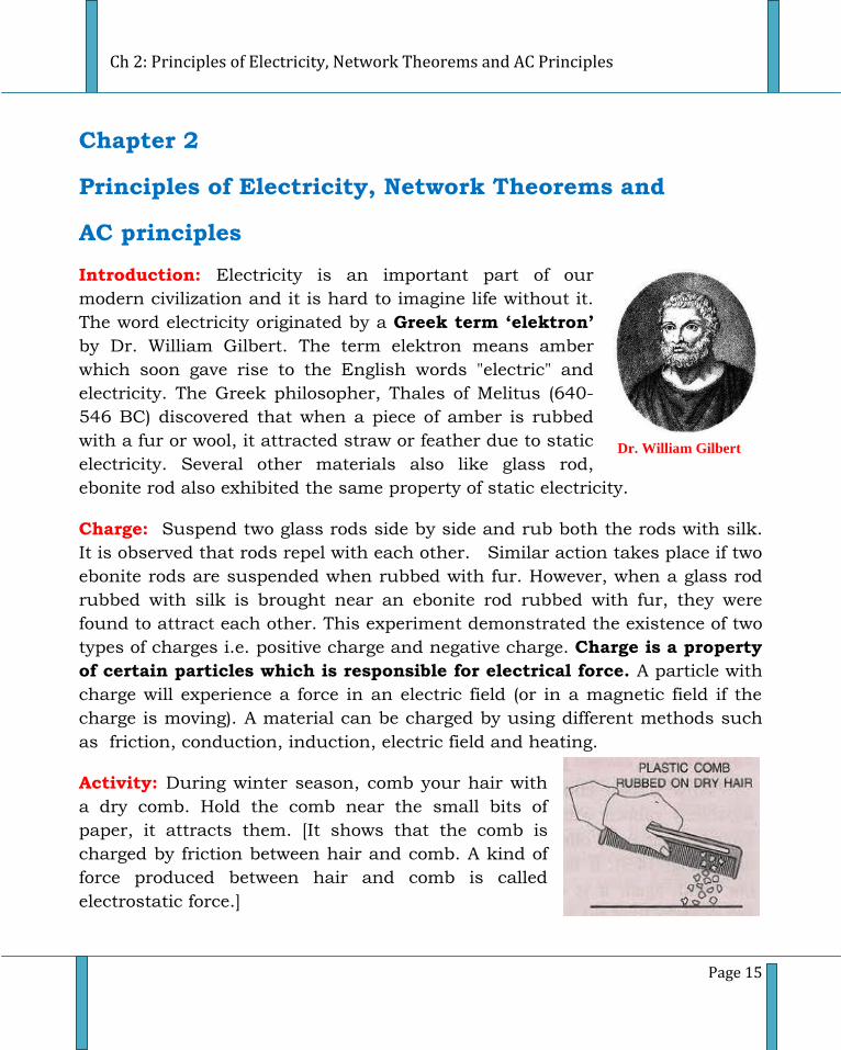
Introduction: Electricity is an important part of our
modern civilization and it is hard to imagine life without it.
The word electricity originated by a Greek term ‘elektron’
by Dr. William Gilbert. The term elektron means amber
which soon gave rise to the English words "electric" and
electricity. The Greek philosopher, Thales of Melitus (640-
546 BC) discovered that when a piece of amber is rubbed
with a fur or wool, it attracted straw or feather due to static
electricity. Several other materials also like glass rod,
ebonite rod also exhibited the same property of static electricity.
Charge: Suspend two glass rods side by side and rub both the rods with silk.
It is observed that rods repel with each other. Similar action takes place if two
ebonite rods are suspended when rubbed with fur. However, when a glass rod
rubbed with silk is brought near an ebonite rod rubbed with fur, they were
found to attract each other. This experiment demonstrated the existence of two
types of charges i.e. positive charge and negative charge. Charge is a property
of certain particles which is responsible for electrical force. A particle with
charge will experience a force in an electric field (or in a magnetic field if the
charge is moving). A material can be charged by using different methods such
as friction, conduction, induction, electric field and heating.
Activity: During winter season, comb your hair with
a dry comb. Hold the comb near the small bits of
paper, it attracts them. [It shows that the comb is
charged by friction between hair and comb. A kind of
force produced between hair and comb is called
electrostatic force.]
Dr. William Gilbert
I PUC Electronics
Page 16
Properties of charges:
1. Like charges repel each other and the unlike charges attract each other.
2. Charges are conserved. It is not possible to neither destroy nor create
charges.
3. Charges reside only on the outer surface of a charged conductor.
4. Charge is not affected by motion.
5. Charge is quantized; i.e., charge can take only integral values. (Q = ± ne).
6. The magnitude of the charge on a single electron (-e) or proton (+e) is 1.60218 × 10 -19 C.
If n electrons pass through a cross section of a conductor in time t, then total charge passed is Q = ne.
The SI unit of charge is coulomb and is denoted by ‘C’. This unit is named after Charles Augustin de Coulomb, a French Physicist who measured the force between charges.
Charge is said to be one Coulomb if one ampere of current flows in one second.
Charge on a single electron is 1.60218 × 10 -19C.
Therefore, 1C =
= Charge on 6.25 ×10 18 electrons.
Thus one coulomb of charge consists of 6.25 ×10 18 electrons
Electric current: The movement of charges through a conductive material
constitutes electric current. The strength of electric current is defined as the
rate of flow of charge through a cross section of a conductor.
If Q is the net amount of charge flowing through a cross-section of a
conductor in a time‘t’ sec, then the steady current I is given by
Current =
I =
=
Ch 2: Principles of Electricity, Network Theorems and AC Principles
Page 17
If ‘dQ’ is the small amount of charge flowing in a small change in time ‘dt’
then the current ‘i’ is given by,
Ampere:
The unit of electric current is said to be 1 ampere, if 1 coulomb of charge
flows through a cross-section of a conductor in 1 second.
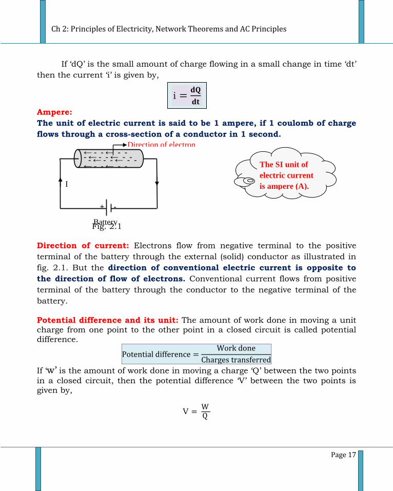
Fig. 2.1
Direction of current: Electrons flow from negative terminal to the positive
terminal of the battery through the external (solid) conductor as illustrated in
fig. 2.1. But the direction of conventional electric current is opposite to
the direction of flow of electrons. Conventional current flows from positive
terminal of the battery through the conductor to the negative terminal of the
battery.
Potential difference and its unit: The amount of work done in moving a unit charge from one point to the other point in a closed circuit is called potential difference.
If ‘w’ is the amount of work done in moving a charge ‘Q’ between the two points
in a closed circuit, then the potential difference ‘V’ between the two points is given by,
V
The SI unit of
electric current
is ampere (A).
i
← - - ← - -
← - - - -
← - - ← - -
← - - - - - ← - - ← - -
← - - - -
- ← - - ← - -
← - - - -
I
+ -
Direction of electron
flow
Battery
(E)
I PUC Electronics
Page 18
The SI unit of potential difference is volt. The potential difference between two points is said to be 1 volt if 1 joule of work is done in moving 1 coulomb of
electric charge from one point to another.
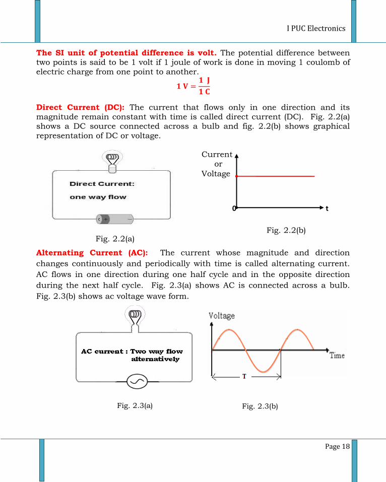
Direct Current (DC): The current that flows only in one direction and its magnitude remain constant with time is called direct current (DC). Fig. 2.2(a) shows a DC source connected across a bulb and fig. 2.2(b) shows graphical
representation of DC or voltage.
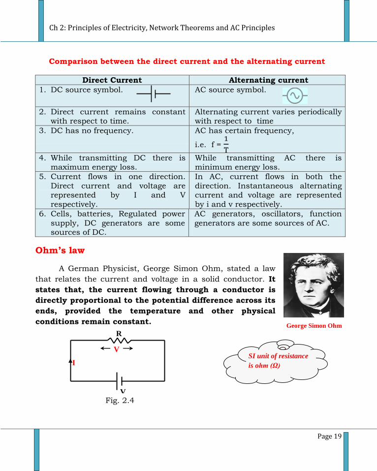
Alternating Current (AC): The current whose magnitude and direction
changes continuously and periodically with time is called alternating current.
AC flows in one direction during one half cycle and in the opposite direction
during the next half cycle. Fig. 2.3(a) shows AC is connected across a bulb.
Fig. 2.3(b) shows ac voltage wave form.
Fig. 2.3(b)
Fig. 2.3(a)
Current
or
Voltage
t 0
Fig. 2.2(b) Fig. 2.2(a)
Ch 2: Principles of Electricity, Network Theorems and AC Principles
Page 19
Comparison between the direct current and the alternating current
Direct Current Alternating current
1. DC source symbol.
AC source symbol.
2. Direct current remains constant with respect to time.
Alternating current varies periodically with respect to time
3. DC has no frequency.
AC has certain frequency,
i.e. f =
4. While transmitting DC there is maximum energy loss.
While transmitting AC there is minimum energy loss.
5. Current flows in one direction.
Direct current and voltage are represented by I and V
respectively.
In AC, current flows in both the
direction. Instantaneous alternating current and voltage are represented
by i and v respectively.
6. Cells, batteries, Regulated power
supply, DC generators are some sources of DC.
AC generators, oscillators, function
generators are some sources of AC.
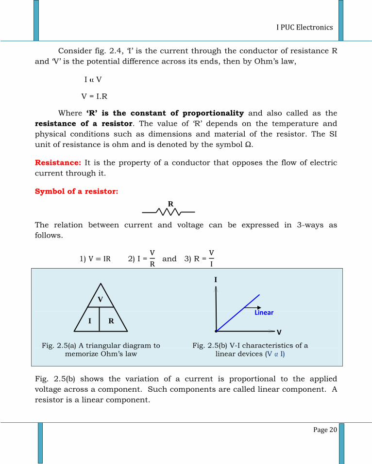
Ohm’s law
A German Physicist, George Simon Ohm, stated a law
that relates the current and voltage in a solid conductor. It
states that, the current flowing through a conductor is
directly proportional to the potential difference across its
ends, provided the temperature and other physical
conditions remain constant.
George Simon Ohm
SI unit of resistance
is ohm (Ω)
Fig. 2.4
I
R
V
V
I PUC Electronics
Page 20
Consider fig. 2.4, ‘I’ is the current through the conductor of resistance R
and ‘V’ is the potential difference across its ends, then by Ohm’s law,
I V
V = I.R
Where ‘R’ is the constant of proportionality and also called as the
resistance of a resistor. The value of ‘R’ depends on the temperature and
physical conditions such as dimensions and material of the resistor. The SI
unit of resistance is ohm and is denoted by the symbol Ω.
Resistance: It is the property of a conductor that opposes the flow of electric
current through it.
Symbol of a resistor:
The relation between current and voltage can be expressed in 3-ways as
follows.
1) 2) I =
and 3) R =
Fig. 2.5(b) shows the variation of a current is proportional to the applied
voltage across a component. Such components are called linear component. A
resistor is a linear component.
V
I R
Fig. 2.5(a) A triangular diagram to memorize Ohm’s law
I
Linear
V
Fig. 2.5(b) V-I characteristics of a
linear devices (V I)
R
Ch 2: Principles of Electricity, Network Theorems and AC Principles
Page 21
Limitations of Ohm’s law:
1. Ohm’s law is not applicable when the physical conditions of a conductor are subjected to change.
2. Ohm’s law is not applicable at extreme low and high temperatures.
3. Ohm’s law is not applicable for non-linear devices such as electron tube, semiconductors, discharge tubes and electrolytes.
4. Ohm’s law is not applicable to arcing devices.
Combination of Resistors:
In electronics, circuits are simplified by simplifying the resistive
network. Normally resistors are connected in Series combination or Parallel
combination.
Series combination of resistors: When one end of resistor is connected
to one end of the other resistor (end to end), they are said to be in series. In this case
1. The current through series resistors remains the same.
2. The voltage divides across series resistor. The voltage drop depends
on the value of resistors.
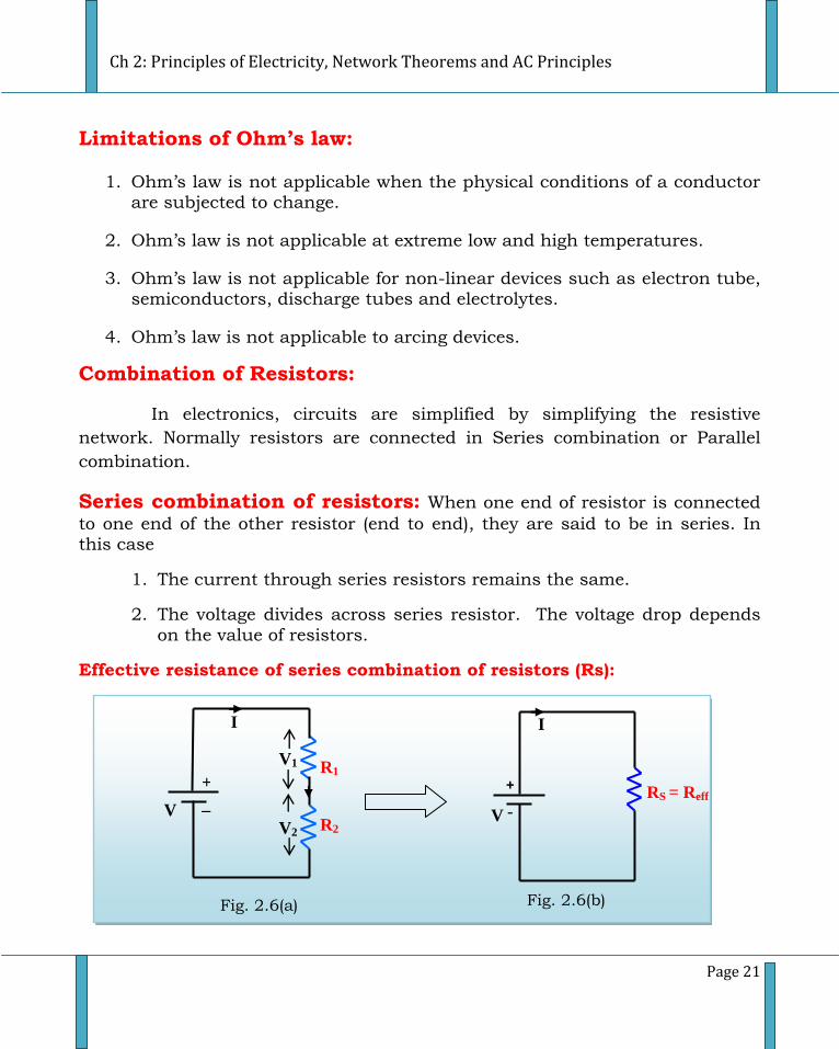
Effective resistance of series combination of resistors (Rs):
I I
V1 R1
_
R2 V2
V
Fig. 2.6(b)
RS = Reff
V
+
-
Fig. 2.6(a)
+
I PUC Electronics
Page 22
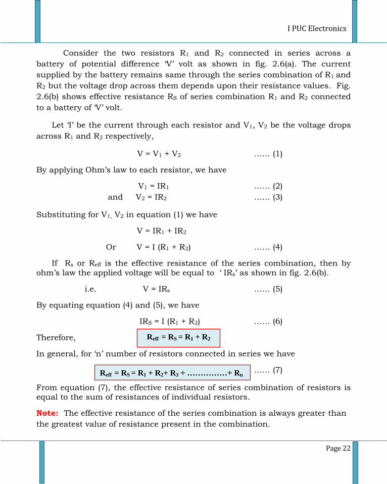
Consider the two resistors R1 and R2 connected in series across a
battery of potential difference ‘V’ volt as shown in fig. 2.6(a). The current
supplied by the battery remains same through the series combination of R1 and
R2 but the voltage drop across them depends upon their resistance values. Fig.
2.6(b) shows effective resistance RS of series combination R1 and R2 connected
to a battery of ‘V’ volt.
Let ‘I’ be the current through each resistor and V1, V2 be the voltage drops
across R1 and R2 respectively,
V = V1 + V2 …… (1)
By applying Ohm’s law to each resistor, we have
V1 = IR1 …… (2)
and V2 = IR2 …… (3)
Substituting for V1, V2 in equation (1) we have
V = IR1 + IR2
Or V = I (R1 + R2) …… (4)
If Rs or Reff is the effective resistance of the series combination, then by
ohm’s law the applied voltage will be equal to ‘ IRs’ as shown in fig. 2.6(b).
i.e. V = IRs …… (5)
By equating equation (4) and (5), we have
IRS = I (R1 + R2) …… (6)
Therefore,
In general, for ‘n’ number of resistors connected in series we have
…… (7)
From equation (7), the effective resistance of series combination of resistors is equal to the sum of resistances of individual resistors.
Note: The effective resistance of the series combination is always greater than
the greatest value of resistance present in the combination.
Reff = RS = R1 + R2
Reff = RS = R1 + R2+ R3 + ……………+ Rn
Ch 2: Principles of Electricity, Network Theorems and AC Principles
Page 23
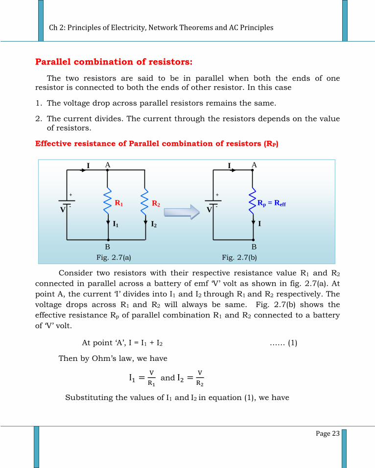
Parallel combination of resistors:
The two resistors are said to be in parallel when both the ends of one resistor is connected to both the ends of other resistor. In this case
1. The voltage drop across parallel resistors remains the same.
2. The current divides. The current through the resistors depends on the value
of resistors.
Effective resistance of Parallel combination of resistors (RP)
Consider two resistors with their respective resistance value R1 and R2
connected in parallel across a battery of emf ‘V’ volt as shown in fig. 2.7(a). At
point A, the current ‘I’ divides into I1 and I2 through R1 and R2 respectively. The
voltage drops across R1 and R2 will always be same. Fig. 2.7(b) shows the
effective resistance Rp of parallel combination R1 and R2 connected to a battery
of ‘V’ volt.
At point ‘A’, I = I1 + I2 …… (1)
Then by Ohm’s law, we have
and
Substituting the values of I1 and I2 in equation (1), we have
Fig. 2.7(a) Fig. 2.7(b)
I
I1
R1
I2
R2 V
+
-
A
B
I
I
Rp = Reff
V
+
-
A
B
I PUC Electronics
Page 24
+
= V[
] …… (2)
If Rp is the effective resistance of the parallel combination of resistors
connected across the same battery of ‘V’ volt as shown in fig. 2.7(b), then by
ohm’s law we have
…… (3)
From equations (2) and (3), we have
= V[
]
Therefore, …… (4)
or
for two resistors in parallel
In general, for ‘n’ number of resistors connected in parallel, we have
..…. (5)
Therefore from equation (5) reveals that, in case of parallel
combination of resistors, the reciprocal of effective resistance is equal to the sum of reciprocals of the individual resistances.
Note:
1. When two equal resistors are in parallel, total resistance reduces to
one half of its resistance value.
2. When three equal resistors are in parallel, total resistance reduces to
one third of its resistance value.
3. When n equal resistors are in parallel, total resistance reduces to
1/nth of its resistance value.
4. The effective resistance of the parallel combination is always less than
the least value of resistance present in the combination.
=
=
Ch 2: Principles of Electricity, Network Theorems and AC Principles
Page 25
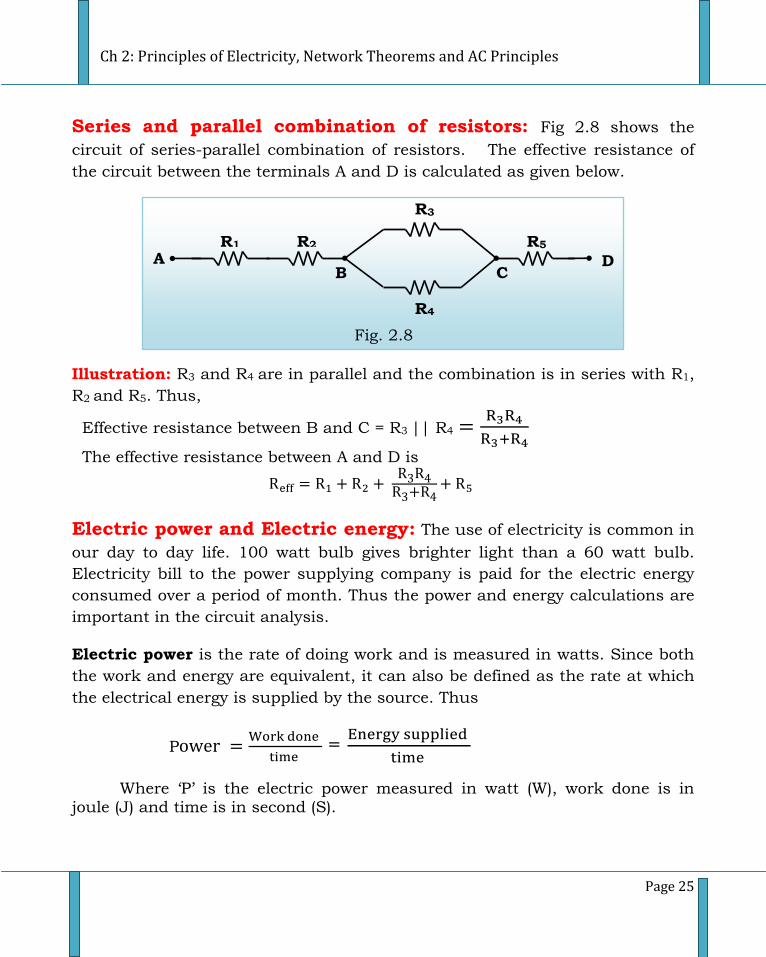
Series and parallel combination of resistors: Fig 2.8 shows the
circuit of series-parallel combination of resistors. The effective resistance of
the circuit between the terminals A and D is calculated as given below.
Illustration: R3 and R4 are in parallel and the combination is in series with R1,
R2 and R5. Thus,
Effective resistance between B and C = R3 || R4
The effective resistance between A and D is
Electric power and Electric energy: The use of electricity is common in
our day to day life. 100 watt bulb gives brighter light than a 60 watt bulb.
Electricity bill to the power supplying company is paid for the electric energy
consumed over a period of month. Thus the power and energy calculations are
important in the circuit analysis.
Electric power is the rate of doing work and is measured in watts. Since both
the work and energy are equivalent, it can also be defined as the rate at which
the electrical energy is supplied by the source. Thus
P
=
Where ‘P’ is the electric power measured in watt (W), work done is in joule (J) and time is in second (S).
R4
R2 R1
Fig. 2.8
C B
R5
D A
R3
I PUC Electronics
Page 26
The electric power is said to be 1 watt, if 1 joule of work is done in 1 second.
Therefore,
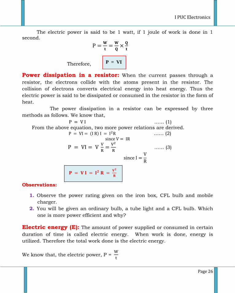
Power dissipation in a resistor: When the current passes through a
resistor, the electrons collide with the atoms present in the resistor. The
collision of electrons converts electrical energy into heat energy. Thus the
electric power is said to be dissipated or consumed in the resistor in the form of
heat.
The power dissipation in a resistor can be expressed by three
methods as follows. We know that,
…… (1) From the above equation, two more power relations are derived.
( ) …… (2)
…… (3)
Observations:
1. Observe the power rating given on the iron box, CFL bulb and mobile
charger.
2. You will be given an ordinary bulb, a tube light and a CFL bulb. Which
one is more power efficient and why?
Electric energy (E): The amount of power supplied or consumed in certain
duration of time is called electric energy. When work is done, energy is
utilized. Therefore the total work done is the electric energy.
We know that, the electric power, P =
P = VI
Ch 2: Principles of Electricity, Network Theorems and AC Principles
Page 27
Where, w → electric energy consumed in a time `t’.
Therefore, electric energy, E = w = P·t
Where P is measured in watt, t in second and w in joule.
The electric bill has to be paid to the power supplying company for the electric energy consumed over a period of month or time. Thus the energy calculation in hour is important. Therefore, P is in watt and t is in hour (60 × 60 sec) then,
Electric energy (E) = w = P × t
1 watt-hour = 1 W × 1 hr
= 1 W × (60 × 60) sec
1 Wh = 3600 joule
The S.I. unit of electrical energy is joule.
Commercial unit of electrical energy:
Actually joule (watt-second) is a very small quantity. Therefore it is
inconvenient to use this unit where a large quantity of energy is involved. So,
for commercial purposes bigger unit of electrical energy i.e., ‘kilowatt-hour’ is
used which is written in short form as kWh.
One kilowatt-hour is the amount of electrical energy consumed
when an electrical appliance having a power rating of 1000 watt is used
for 1 hour. kWh is called the commercial unit or Board Of Trade (BOT)
unit or simply one unit.
Therefore
I PUC Electronics
Page 28
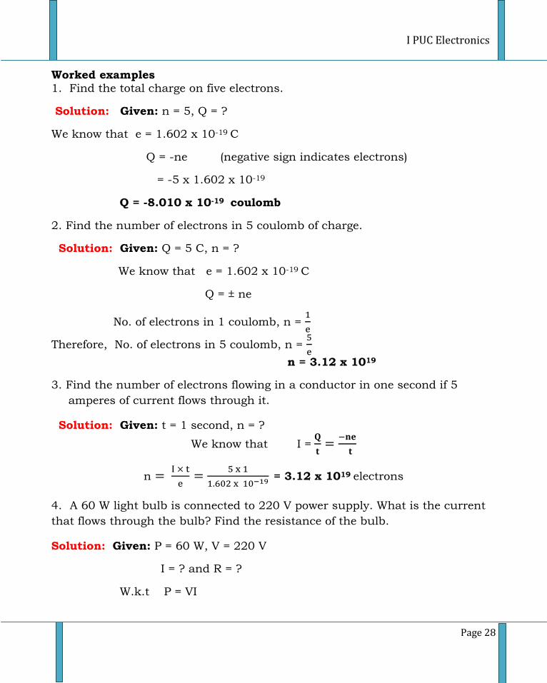
Worked examples 1. Find the total charge on five electrons.
Solution: Given: n = 5, Q = ?
We know that e = 1.602 x 10⁻¹⁹ C
Q = -ne (negative sign indicates electrons)
= -5 x 1.602 x 10-19
Q = -8.010 x 10⁻¹⁹ coulomb
2. Find the number of electrons in 5 coulomb of charge.
Solution: Given: Q = 5 C, n = ?
We know that e = 1.602 x 10⁻¹⁹ C
Q = ± ne
No. of electrons in 1 coulomb, n =
Therefore, No. of electrons in 5 coulomb, n =
n = 3.12 x 10¹⁹
3. Find the number of electrons flowing in a conductor in one second if 5
amperes of current flows through it.
Solution: Given: t = 1 second, n = ?
We know that I =
n
= 3.12 x 10¹⁹
electrons
4. A 60 W light bulb is connected to 220 V power supply. What is the current
that flows through the bulb? Find the resistance of the bulb.
Solution: Given: P = 60 W, V = 220 V
I = ? and R = ?
W.k.t P = VI
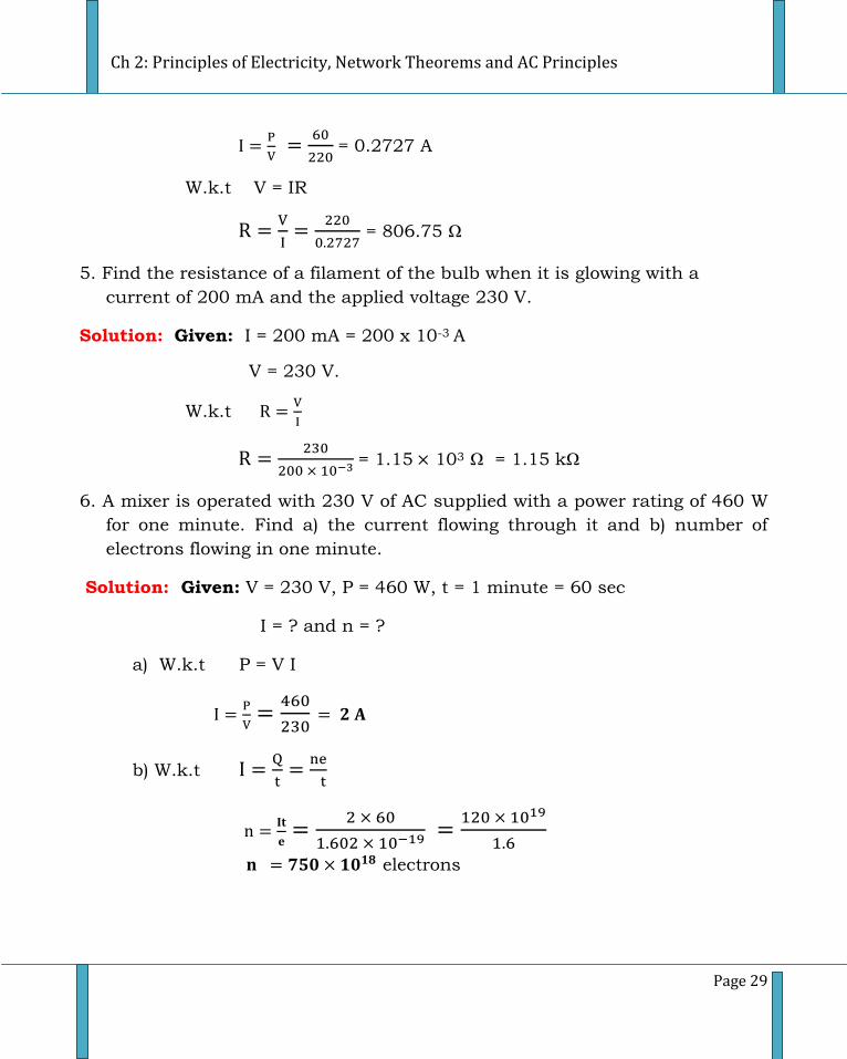
Ch 2: Principles of Electricity, Network Theorems and AC Principles
Page 29
= 0.2727 A
W.k.t V = IR
= 806.75 Ω
5. Find the resistance of a filament of the bulb when it is glowing with a
current of 200 mA and the applied voltage 230 V.
Solution: Given: I = 200 mA = 200 x 10-3 A
V = 230 V.
W.k.t
= 1.15 103 Ω = 1.15 kΩ
6. A mixer is operated with 230 V of AC supplied with a power rating of 460 W
for one minute. Find a) the current flowing through it and b) number of
electrons flowing in one minute.
Solution: Given: V = 230 V, P = 460 W, t = 1 minute = 60 sec
I = ? and n = ?
a) W.k.t P = V I
b) W.k.t
electrons
I PUC Electronics
Page 30
7. Find the power consumed by a telephone when operated with a 9 V and
200 mA of current.
Solution: Given: V = 9 V, I = 200 mA = 200 x 10-3 A and P = ?
We know that (w.k.t) P = VI = 9 x 200 x 10-3 W = 1.8 W
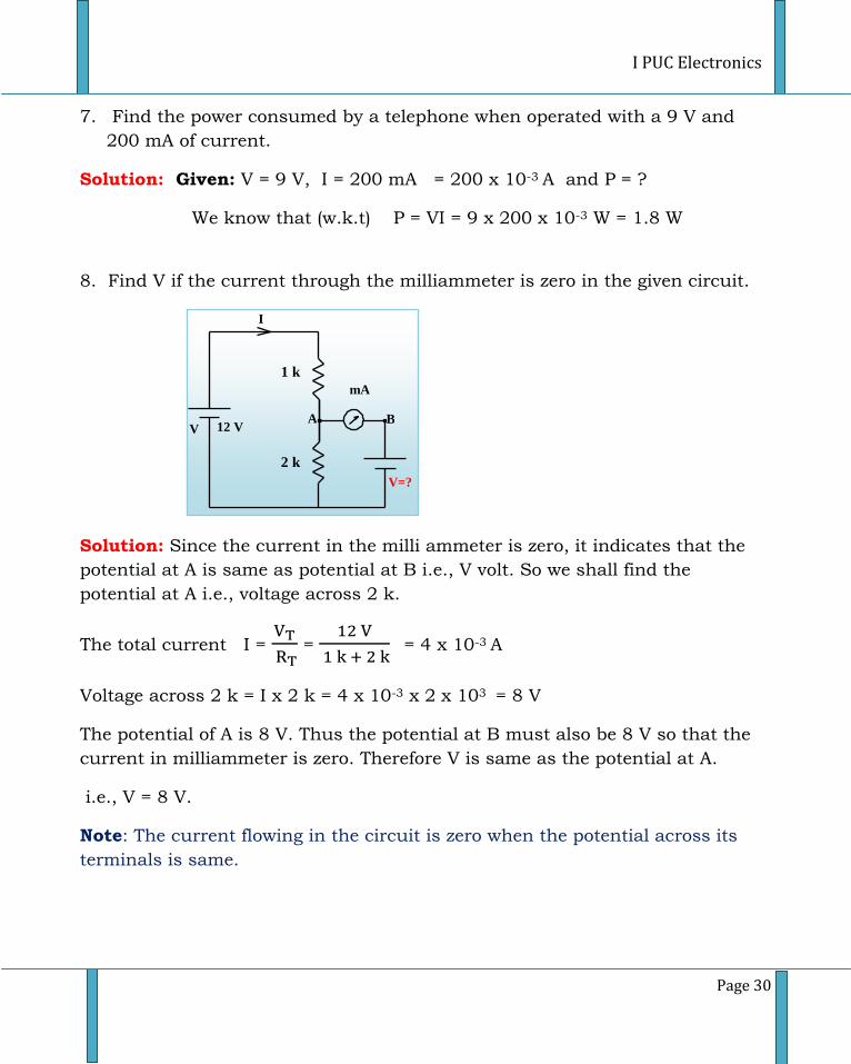
8. Find V if the current through the milliammeter is zero in the given circuit.
Solution: Since the current in the milli ammeter is zero, it indicates that the
potential at A is same as potential at B i.e., V volt. So we shall find the
potential at A i.e., voltage across 2 k.
The total current I =
=
= 4 x 10⁻³ A
Voltage across 2 k = I x 2 k = 4 x 10-3 x 2 x 103 = 8 V
The potential of A is 8 V. Thus the potential at B must also be 8 V so that the
current in milliammeter is zero. Therefore V is same as the potential at A.
i.e., V = 8 V.
Note: The current flowing in the circuit is zero when the potential across its
terminals is same.
1 k
12 V
2 k
I
mA
B A V
V=?
Ch 2: Principles of Electricity, Network Theorems and AC Principles
Page 31
9. Find the total resistance of the series combination of resistors 5 kΩ, 10 kΩ
and 15 kΩ.
Solution: W.k.t, for series combination,
The total resistance RS = RT = R1 + R2 + R3 = 5 k + 10 k + 15 k = 30 kΩ
10. Find the total resistance when the three 30 kΩ resistors are connected in parallel.
Solution: W.k.t for parallel combination of resistors,
RT 10 kΩ
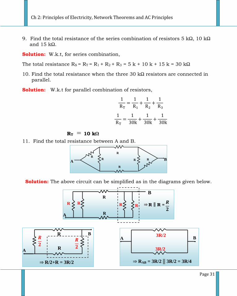
11. Find the total resistance between A and B.
Solution: The above circuit can be simplified as in the diagrams given below.
R
R
R R R
B
A
R R = R
R
R
R R R R
A B
R
R
B
A
R/2+R = 3R/2
3R/2
3R/2
B A
RAB = 3R/2 || 3R/2 = 3R/4
I PUC Electronics
Page 32
R R R
A B
A B
R
R
R
A B
VS
Therefore, total resistance between A and B
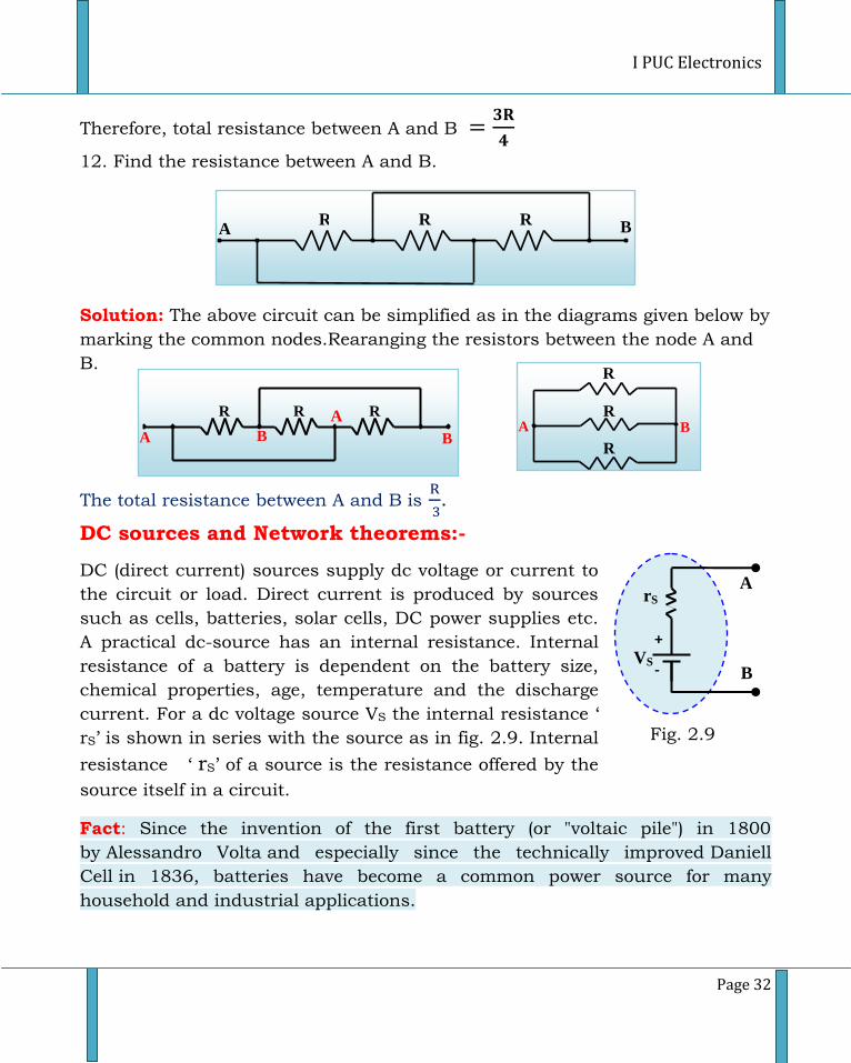
12. Find the resistance between A and B.
Solution: The above circuit can be simplified as in the diagrams given below by
marking the common nodes.Rearanging the resistors between the node A and
B.
The total resistance between A and B is
.
DC sources and Network theorems:-
DC (direct current) sources supply dc voltage or current to
the circuit or load. Direct current is produced by sources
such as cells, batteries, solar cells, DC power supplies etc.
A practical dc-source has an internal resistance. Internal
resistance of a battery is dependent on the battery size,
chemical properties, age, temperature and the discharge
current. For a dc voltage source VS the internal resistance ‘
rS’ is shown in series with the source as in fig. 2.9. Internal
resistance ‘ rS’ of a source is the resistance offered by the
source itself in a circuit.
Fact: Since the invention of the first battery (or "voltaic pile") in 1800
by Alessandro Volta and especially since the technically improved Daniell
Cell in 1836, batteries have become a common power source for many
household and industrial applications.
R R R A B
Fig. 2.9
A
B
+ VS
rS
-
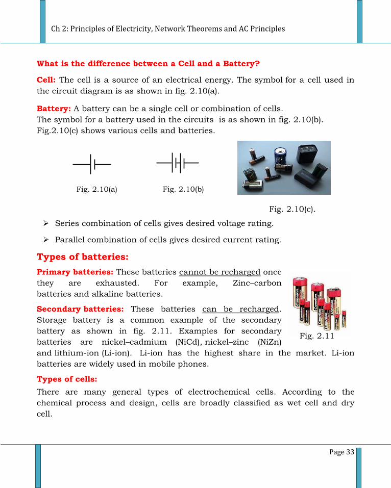
Ch 2: Principles of Electricity, Network Theorems and AC Principles
Page 33
What is the difference between a Cell and a Battery?
Cell: The cell is a source of an electrical energy. The symbol for a cell used in
the circuit diagram is as shown in fig. 2.10(a).
Battery: A battery can be a single cell or combination of cells.
The symbol for a battery used in the circuits is as shown in fig. 2.10(b).
Fig.2.10(c) shows various cells and batteries.
Series combination of cells gives desired voltage rating.
Parallel combination of cells gives desired current rating.
Types of batteries:
Primary batteries: These batteries cannot be recharged once
they are exhausted. For example, Zinc–carbon
batteries and alkaline batteries.
Secondary batteries: These batteries can be recharged.
Storage battery is a common example of the secondary
battery as shown in fig. 2.11. Examples for secondary
batteries are nickel–cadmium (NiCd), nickel–zinc (NiZn)
and lithium-ion (Li-ion). Li-ion has the highest share in the market. Li-ion
batteries are widely used in mobile phones.
Types of cells:
There are many general types of electrochemical cells. According to the
chemical process and design, cells are broadly classified as wet cell and dry
cell.
Fig. 2.10(b) Fig. 2.10(a)
Fig. 2.10(c).
Fig. 2.11
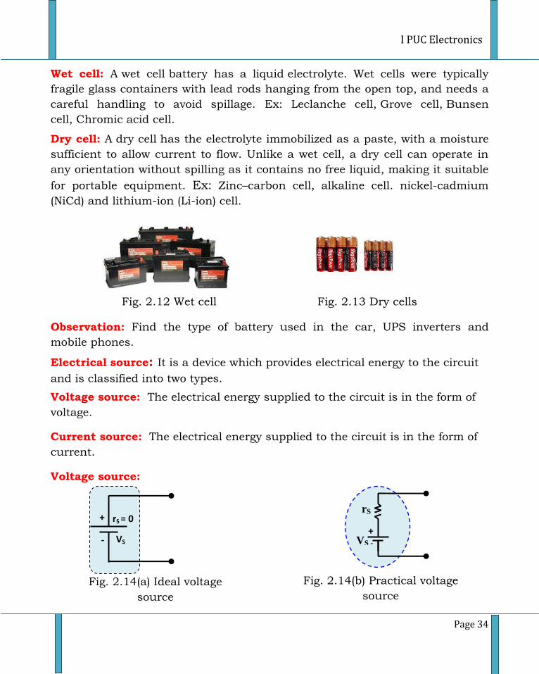
I PUC Electronics
Page 34
Wet cell: A wet cell battery has a liquid electrolyte. Wet cells were typically
fragile glass containers with lead rods hanging from the open top, and needs a
careful handling to avoid spillage. Ex: Leclanche cell, Grove cell, Bunsen
cell, Chromic acid cell.
Dry cell: A dry cell has the electrolyte immobilized as a paste, with a moisture
sufficient to allow current to flow. Unlike a wet cell, a dry cell can operate in
any orientation without spilling as it contains no free liquid, making it suitable
for portable equipment. Ex: Zinc–carbon cell, alkaline cell. nickel-cadmium
(NiCd) and lithium-ion (Li-ion) cell.
Observation: Find the type of battery used in the car, UPS inverters and
mobile phones.
Electrical source: It is a device which provides electrical energy to the circuit
and is classified into two types.
Voltage source: The electrical energy supplied to the circuit is in the form of
voltage.
Current source: The electrical energy supplied to the circuit is in the form of
current.
Voltage source:
Fig. 2.12 Wet cell Fig. 2.13 Dry cells
Fig. 2.14(a) Ideal voltage
source
Fig. 2.14(b) Practical voltage
source
+ VS -
rS
-
+ rS = 0
VS
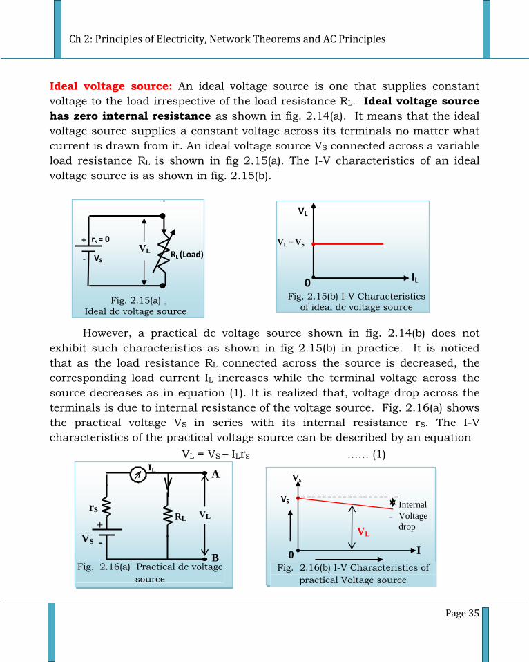
Ch 2: Principles of Electricity, Network Theorems and AC Principles
Page 35
Ideal voltage source: An ideal voltage source is one that supplies constant
voltage to the load irrespective of the load resistance RL. Ideal voltage source
has zero internal resistance as shown in fig. 2.14(a). It means that the ideal
voltage source supplies a constant voltage across its terminals no matter what
current is drawn from it. An ideal voltage source VS connected across a variable
load resistance RL is shown in fig 2.15(a). The I-V characteristics of an ideal
voltage source is as shown in fig. 2.15(b).
However, a practical dc voltage source shown in fig. 2.14(b) does not
exhibit such characteristics as shown in fig 2.15(b) in practice. It is noticed
that as the load resistance RL connected across the source is decreased, the
corresponding load current IL increases while the terminal voltage across the
source decreases as in equation (1). It is realized that, voltage drop across the
terminals is due to internal resistance of the voltage source. Fig. 2.16(a) shows
the practical voltage VS in series with its internal resistance rS. The I-V
characteristics of the practical voltage source can be described by an equation
VL = VS – ILrS ..…. (1)
+
- RL (Load) VS VL
rs = 0
Fig. 2.15(a)
Ideal dc voltage source
IL 0
Fig. 2.15(b) I-V Characteristics
of ideal dc voltage source
VL = VS
VL
RL
VL= VO
Fig. 2.16(b) I-V Characteristics of
practical Voltage source
Internal
Voltage
drop
0 I
L
Vs
VS
VL
Fig. 2.16(a) Practical dc voltage
source
IL
rS
-
+
VS
B
A
RL VL
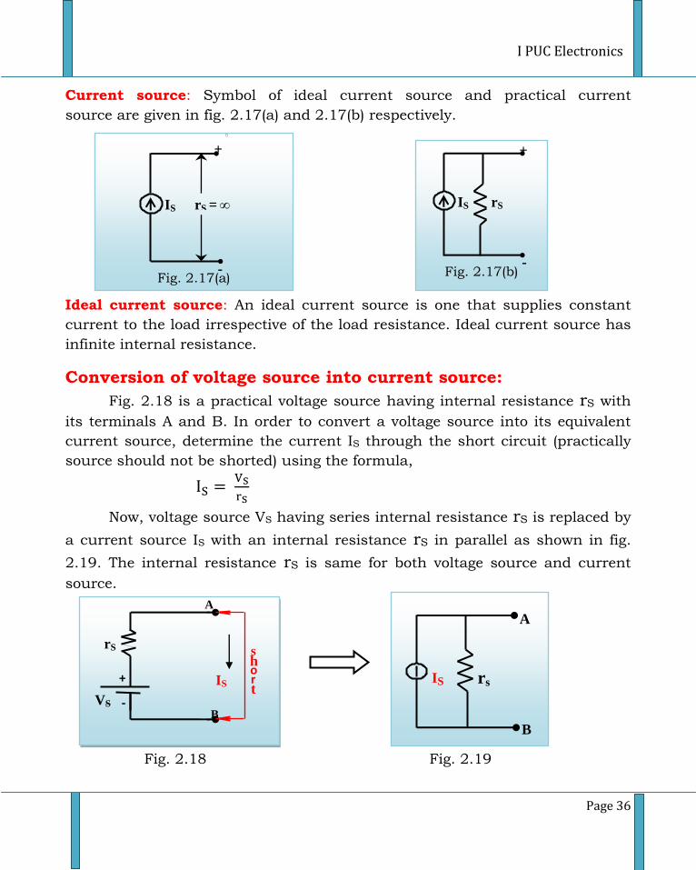
I PUC Electronics
Page 36
Current source: Symbol of ideal current source and practical current
source are given in fig. 2.17(a) and 2.17(b) respectively.
Ideal current source: An ideal current source is one that supplies constant
current to the load irrespective of the load resistance. Ideal current source has
infinite internal resistance.
Conversion of voltage source into current source:
Fig. 2.18 is a practical voltage source having internal resistance rS with
its terminals A and B. In order to convert a voltage source into its equivalent
current source, determine the current IS through the short circuit (practically
source should not be shorted) using the formula,
Now, voltage source VS having series internal resistance rS is replaced by
a current source IS with an internal resistance rS in parallel as shown in fig.
2.19. The internal resistance rS is same for both voltage source and current
source.
Fig. 2.18 Fig. 2.19
rS IS
+
- Fig. 2.17(b)
IS
B
rs
A
rS = ∞ IS
+
- Fig. 2.17(a)
B
+
- VS
s h o r t
rS
A
IS
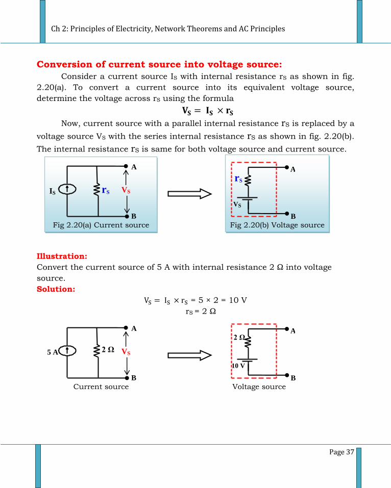
Ch 2: Principles of Electricity, Network Theorems and AC Principles
Page 37
Conversion of current source into voltage source:
Consider a current source IS with internal resistance rS as shown in fig.
2.20(a). To convert a current source into its equivalent voltage source,
determine the voltage across rS using the formula
Now, current source with a parallel internal resistance rS is replaced by a
voltage source VS with the series internal resistance rS as shown in fig. 2.20(b).
The internal resistance rS is same for both voltage source and current source.
Illustration:
Convert the current source of 5 A with internal resistance 2 Ω into voltage
source.
Solution:
= 5 × 2 = 10 V
rS = 2 Ω
Fig 2.20(b) Voltage source Fig 2.20(a) Current source
B
A
VS IS rS
rS
VS
B
A
Voltage source
2 Ω
10 V
B
A
Current source
B
A
VS 5 A 2 Ω
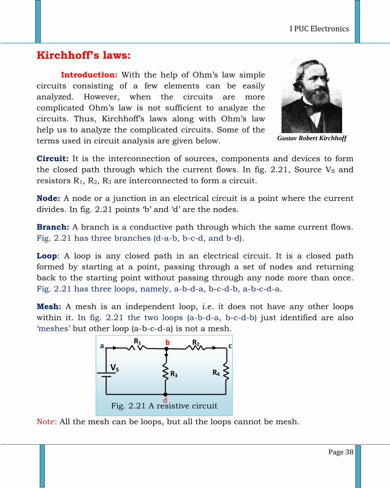
I PUC Electronics
Page 38
Kirchhoff’s laws:
Introduction: With the help of Ohm’s law simple
circuits consisting of a few elements can be easily
analyzed. However, when the circuits are more
complicated Ohm’s law is not sufficient to analyze the
circuits. Thus, Kirchhoff’s laws along with Ohm’s law
help us to analyze the complicated circuits. Some of the
terms used in circuit analysis are given below.
Circuit: It is the interconnection of sources, components and devices to form
the closed path through which the current flows. In fig. 2.21, Source VS and
resistors R1, R2, R3 are interconnected to form a circuit.
Node: A node or a junction in an electrical circuit is a point where the current
divides. In fig. 2.21 points ‘b’ and ‘d’ are the nodes.
Branch: A branch is a conductive path through which the same current flows.
Fig. 2.21 has three branches (d-a-b, b-c-d, and b-d).
Loop: A loop is any closed path in an electrical circuit. It is a closed path
formed by starting at a point, passing through a set of nodes and returning
back to the starting point without passing through any node more than once.
Fig. 2.21 has three loops, namely, a-b-d-a, b-c-d-b, a-b-c-d-a.
Mesh: A mesh is an independent loop, i.e. it does not have any other loops
within it. In fig. 2.21 the two loops (a-b-d-a, b-c-d-b) just identified are also
‘meshes’ but other loop (a-b-c-d-a) is not a mesh.
Note: All the mesh can be loops, but all the loops cannot be mesh.
R1
R2
R3
d
a c b
VS
Fig. 2.21 A resistive circuit
R4
Gustav Robert Kirchhoff
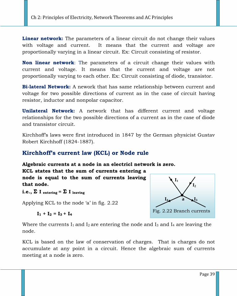
Ch 2: Principles of Electricity, Network Theorems and AC Principles
Page 39
Linear network: The parameters of a linear circuit do not change their values
with voltage and current. It means that the current and voltage are
proportionally varying in a linear circuit. Ex: Circuit consisting of resistor.
Non linear network: The parameters of a circuit change their values with
current and voltage. It means that the current and voltage are not
proportionally varying to each other. Ex: Circuit consisting of diode, transistor.
Bi-lateral Network: A nework that has same relationship between current and
voltage for two possible directions of current as in the case of circuit having
resistor, inductor and nonpolar capacitor.
Unilateral Network: A network that has different current and voltage
relationships for the two possible directions of a current as in the case of diode
and transistor circuit.
Kirchhoff’s laws were first introduced in 1847 by the German physicist Gustav
Robert Kirchhoff (1824-1887).
Kirchhoff’s current law (KCL) or Node rule
Algebraic currents at a node in an electricl network is zero.
KCL states that the sum of currents entering a
node is equal to the sum of currents leaving
that node.
i.e., Σ I entering = Σ I leaving
Applying KCL to the node ‘a’ in fig. 2.22
I1 + I2 = I3 + I4
Where the currents I1 and I2 are entering the node and I3 and I4 are leaving the
node.
KCL is based on the law of conservation of charges. That is charges do not
accumulate at any point in a circuit. Hence the algebraic sum of currents
meeting at a node is zero.
I1
a I3 I4
I2
Fig. 2.22 Branch currents
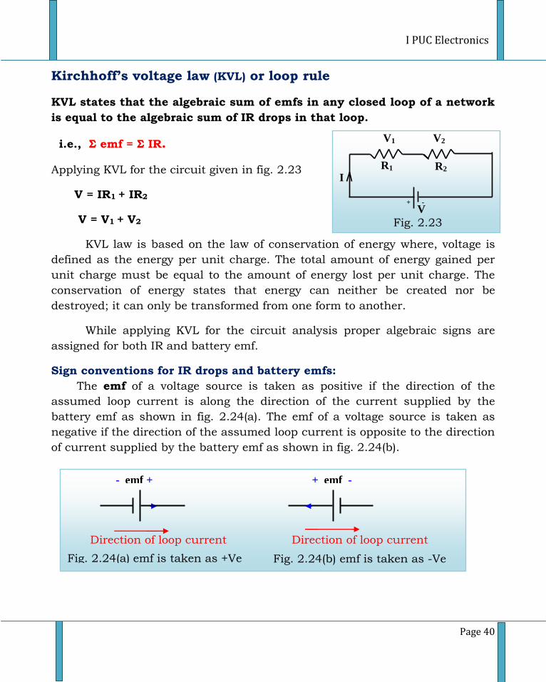
I PUC Electronics
Page 40
V2
I
V
R2
+ -
R1
V1
Fig. 2.23
Kirchhoff’s voltage law (KVL) or loop rule
KVL states that the algebraic sum of emfs in any closed loop of a network
is equal to the algebraic sum of IR drops in that loop.
i.e., Σ emf = Σ IR.
Applying KVL for the circuit given in fig. 2.23
V = IR1 + IR2
V = V1 + V2
KVL law is based on the law of conservation of energy where, voltage is
defined as the energy per unit charge. The total amount of energy gained per
unit charge must be equal to the amount of energy lost per unit charge. The
conservation of energy states that energy can neither be created nor be
destroyed; it can only be transformed from one form to another.
While applying KVL for the circuit analysis proper algebraic signs are
assigned for both IR and battery emf.
Sign conventions for IR drops and battery emfs:
The emf of a voltage source is taken as positive if the direction of the
assumed loop current is along the direction of the current supplied by the
battery emf as shown in fig. 2.24(a). The emf of a voltage source is taken as
negative if the direction of the assumed loop current is opposite to the direction
of current supplied by the battery emf as shown in fig. 2.24(b).
+ emf -
Direction of loop current Direction of loop current
Fig. 2.24(a) emf is taken as +Ve Fig. 2.24(b) emf is taken as -Ve
- emf +
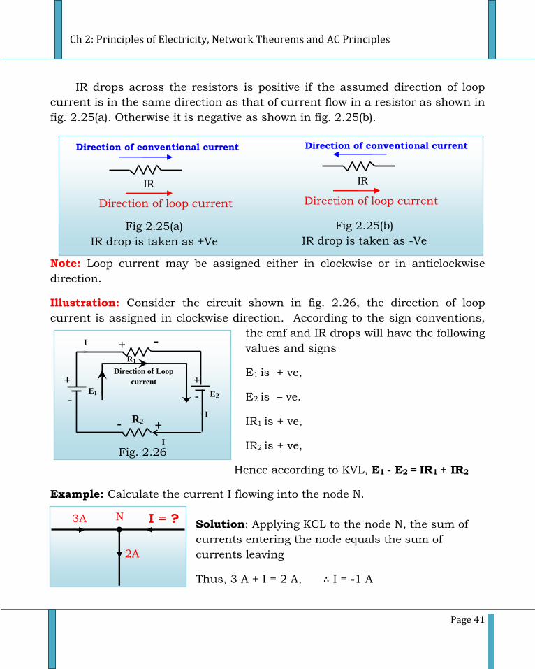
Ch 2: Principles of Electricity, Network Theorems and AC Principles
Page 41
+
- E1
I
R2
E2
Direction of Loop
current
+
+
+ -
-
-
I
Fig. 2.26
I
R1
IR drops across the resistors is positive if the assumed direction of loop
current is in the same direction as that of current flow in a resistor as shown in
fig. 2.25(a). Otherwise it is negative as shown in fig. 2.25(b).
Note: Loop current may be assigned either in clockwise or in anticlockwise
direction.
Illustration: Consider the circuit shown in fig. 2.26, the direction of loop
current is assigned in clockwise direction. According to the sign conventions,
the emf and IR drops will have the following
values and signs
E1 is + ve,
E2 is – ve.
IR1 is + ve,
IR2 is + ve,
Hence according to KVL, E1 - E2 = IR1 + IR2
Example: Calculate the current I flowing into the node N.
Solution: Applying KCL to the node N, the sum of
currents entering the node equals the sum of
currents leaving
Thus, 3 A + I = 2 A, I = -1 A
IR
Direction of loop current
Direction of conventional current
IR
Direction of loop current
Fig 2.25(a)
IR drop is taken as +Ve
Fig 2.25(b)
IR drop is taken as -Ve
Direction of conventional current
3A
2A
I = ? N
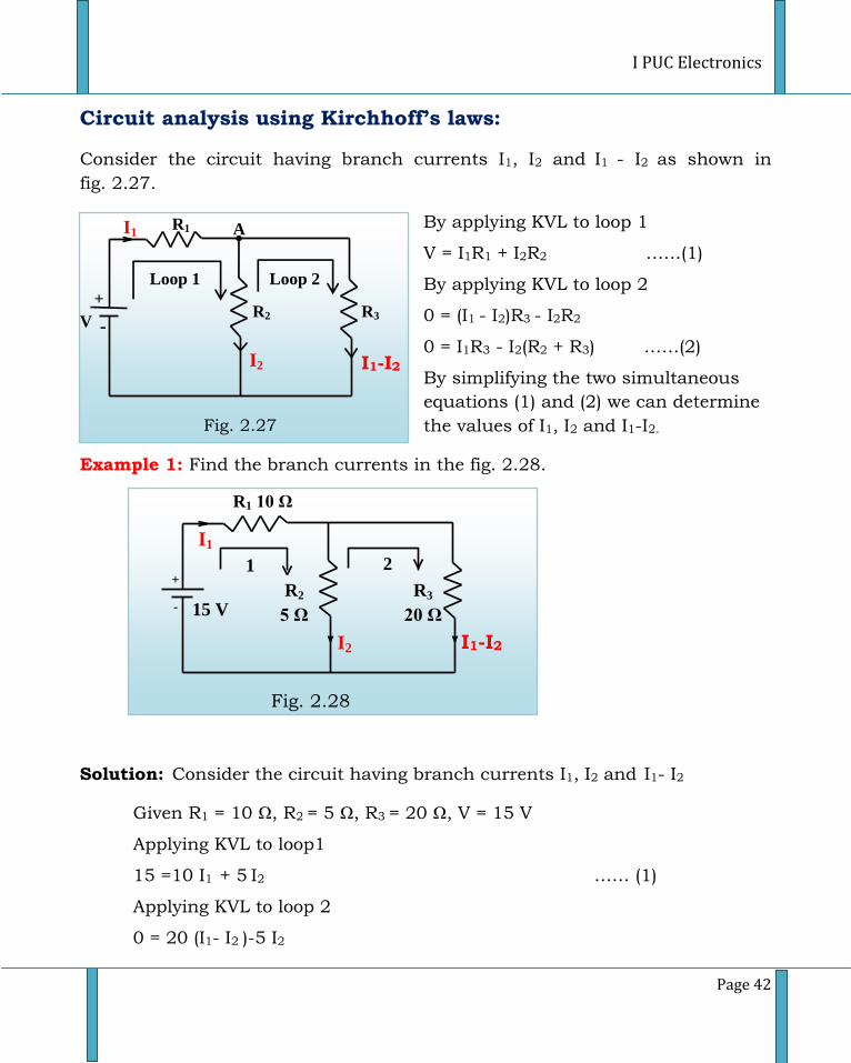
I PUC Electronics
Page 42
+
- 15 V
I2 I1-I2
1 2
R2
5 Ω
I1
R3
20 Ω
Fig. 2.28
R1 10 Ω
Circuit analysis using Kirchhoff’s laws:
Consider the circuit having branch currents I1, I2 and I1 - I2 as shown in
fig. 2.27.
By applying KVL to loop 1
V = I1R1 + I2R2 ……(1)
By applying KVL to loop 2
0 = (I1 - I2)R3 - I2R2
0 = I1R3 - I2(R2 + R3) ……(2)
By simplifying the two simultaneous
equations (1) and (2) we can determine
the values of I1, I2 and I1-I2.
Example 1: Find the branch currents in the fig. 2.28.
Solution: Consider the circuit having branch currents I1, I2 and I1- I2
Given R1 = 10 Ω, R2 = 5 Ω, R3 = 20 Ω, V = 15 V
Applying KVL to loop1
15 =10 I1 + 5 I2 …… (1)
Applying KVL to loop 2
0 = 20 (I1- I2 )-5 I2
R2
I1
+
- V
I2
Loop 1 Loop 2
R3
R1
I1-I2
A
Fig. 2.27
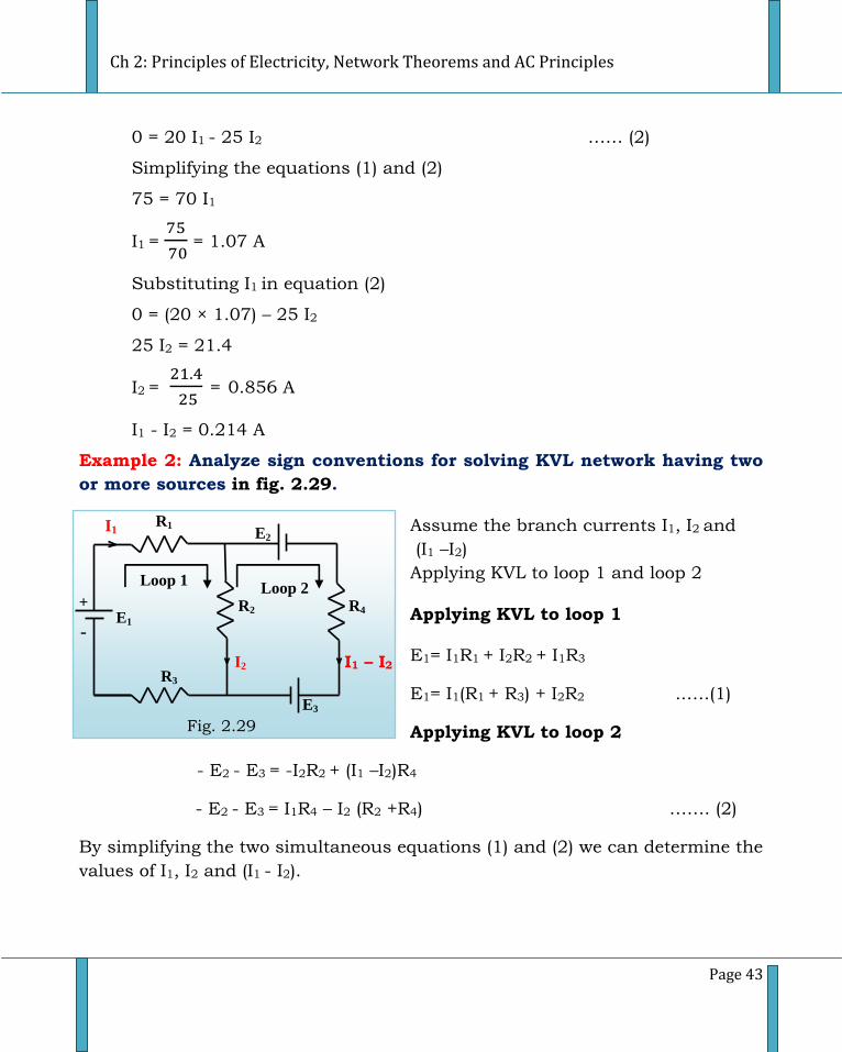
Ch 2: Principles of Electricity, Network Theorems and AC Principles
Page 43
+
- E1
I2 I1 – I2
I1 E2
E3
R3
R2 R4 Loop 2 Loop 1
R1
Fig. 2.29
0 = 20 I1 - 25 I2 …… (2)
Simplifying the equations (1) and (2)
75 = 70 I1
I1 =
= 1.07 A
Substituting I1 in equation (2)
0 = (20 × 1.07) – 25 I2
25 I2 = 21.4
I2 =
= 0.856 A
I1 - I2 = 0.214 A
Example 2: Analyze sign conventions for solving KVL network having two
or more sources in fig. 2.29.
Assume the branch currents I1, I2 and
(I1 –I2)
Applying KVL to loop 1 and loop 2
Applying KVL to loop 1
E1= I1R1 + I2R2 + I1R3
E1= I1(R1 + R3) + I2R2 ..….(1)
Applying KVL to loop 2
- E2 - E3 = -I2R2 + (I1 –I2)R4
- E2 - E3 = I1R4 – I2 (R2 +R4) ……. (2)
By simplifying the two simultaneous equations (1) and (2) we can determine the
values of I1, I2 and (I1 - I2).
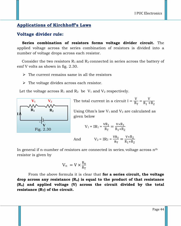
I PUC Electronics
Page 44
Applications of Kirchhoff’s Laws
Voltage divider rule:
Series combination of resistors forms voltage divider circuit. The
applied voltage across the series combination of resistors is divided into a
number of voltage drops across each resistor.
Consider the two resistors R1 and R2 connected in series across the battery of
emf V volts as shown in fig. 2.30.
The current remains same in all the resistors
The voltage divides across each resistor.
Let the voltage across R1 and R2 be V1 and V2 respectively.
The total current in a circuit
Using Ohm’s law V1 and V2 are calculated as
given below
V1 = IR1 =
And V2 = IR2 =
In general if n-number of resistors are connected in series, voltage across nth
resistor is given by
Vn
From the above formula it is clear that for a series circuit, the voltage
drop across any resistance (Rn) is equal to the product of that resistance
(Rn) and applied voltage (V) across the circuit divided by the total
resistance (RT) of the circuit.
V2
I
V
R2
+ -
R1
V1
Fig. 2.30
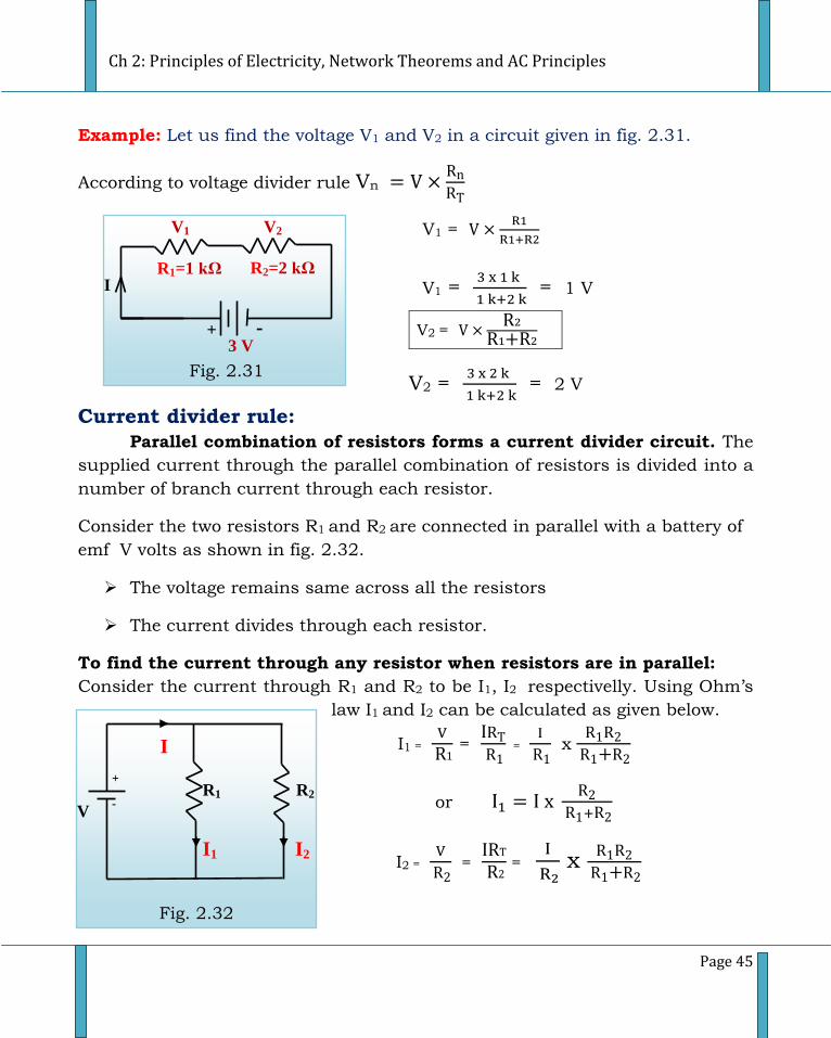
Ch 2: Principles of Electricity, Network Theorems and AC Principles
Page 45
I1
V
+
-
I2
R1 R2
I
Fig. 2.32
Example: Let us find the voltage V1 and V2 in a circuit given in fig. 2.31.
According to voltage divider rule Vn
V1 =
= 1 V
V2 =
= 2 V
Current divider rule:
Parallel combination of resistors forms a current divider circuit. The
supplied current through the parallel combination of resistors is divided into a
number of branch current through each resistor.
Consider the two resistors R1 and R2 are connected in parallel with a battery of
emf V volts as shown in fig. 2.32.
The voltage remains same across all the resistors
The current divides through each resistor.
To find the current through any resistor when resistors are in parallel:
Consider the current through R1 and R2 to be I1, I2 respectivelly. Using Ohm’s
law I1 and I2 can be calculated as given below.
I1 =
=
=
x
or
I2 =
=
=
x
V1 =
V2 =
I
3 V
R1=1 kΩ
+ -
R2=2 kΩ
V1 V2
Fig. 2.31
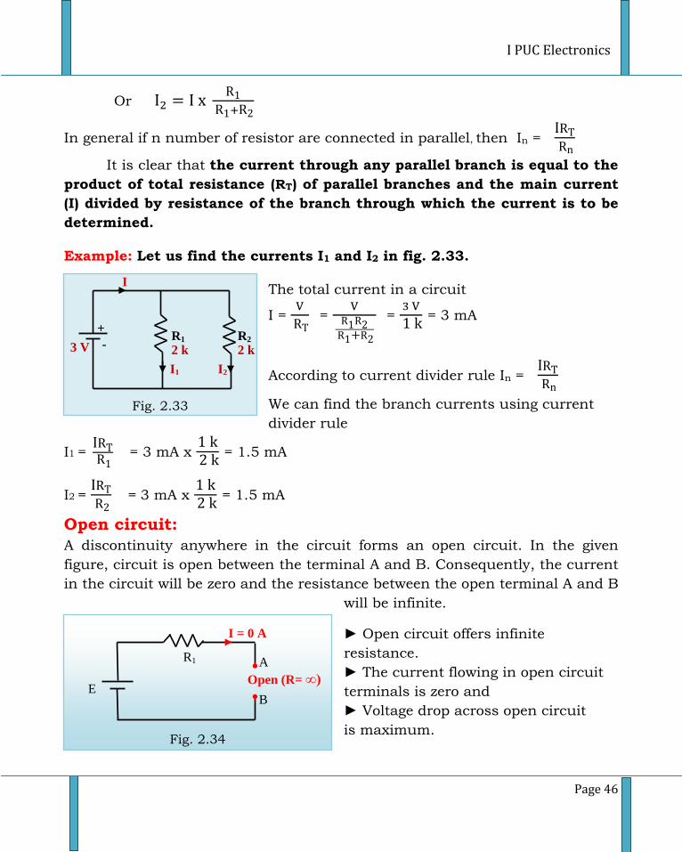
I PUC Electronics
Page 46
Or
In general if n number of resistor are connected in parallel, then In =
It is clear that the current through any parallel branch is equal to the
product of total resistance (RT) of parallel branches and the main current
(I) divided by resistance of the branch through which the current is to be
determined.
Example: Let us find the currents I1 and I2 in fig. 2.33.
The total current in a circuit
I =
=
=
= 3 mA
According to current divider rule In =
We can find the branch currents using current
divider rule
I1 =
= 3 mA x
= 1.5 mA
I2 =
= 3 mA x
= 1.5 mA
Open circuit:
A discontinuity anywhere in the circuit forms an open circuit. In the given
figure, circuit is open between the terminal A and B. Consequently, the current
in the circuit will be zero and the resistance between the open terminal A and B
will be infinite.
Open circuit offers infinite
resistance.
The current flowing in open circuit
terminals is zero and
Voltage drop across open circuit
is maximum.
E
A
I = 0 A
Open (R= ∞)
B
Fig. 2.34
R1
I
I1
R1 3 V
+ -
R2
2 k 2 k
I2
Fig. 2.33
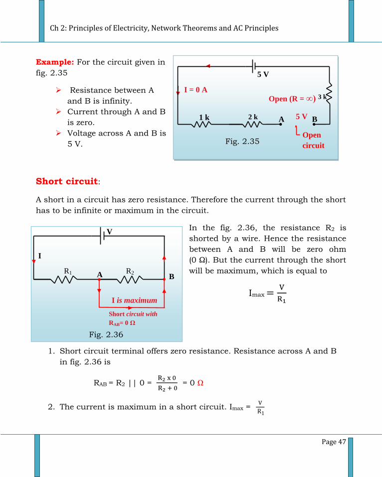
Ch 2: Principles of Electricity, Network Theorems and AC Principles
Page 47
3 k
2 k 1 k
Fig. 2.35
Open
circuit
I = 0 A
5 V
Open (R = ∞)
5 V A B
Example: For the circuit given in
fig. 2.35
Resistance between A
and B is infinity.
Current through A and B
is zero.
Voltage across A and B is
5 V.
Short circuit:
A short in a circuit has zero resistance. Therefore the current through the short
has to be infinite or maximum in the circuit.
In the fig. 2.36, the resistance R2 is
shorted by a wire. Hence the resistance
between A and B will be zero ohm
(0 Ω). But the current through the short
will be maximum, which is equal to
Imax
1. Short circuit terminal offers zero resistance. Resistance across A and B
in fig. 2.36 is
RAB = R2 || 0 =
= 0 Ω
2. The current is maximum in a short circuit. Imax =
V
B
I
A
Short circuit with
RAB= 0 Ω
I is maximum
R1 R2
Fig. 2.36
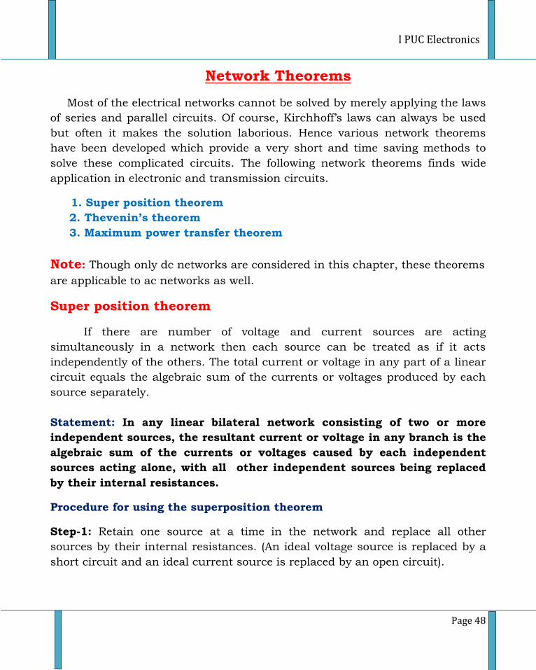
I PUC Electronics
Page 48
Network Theorems
Most of the electrical networks cannot be solved by merely applying the laws
of series and parallel circuits. Of course, Kirchhoff’s laws can always be used
but often it makes the solution laborious. Hence various network theorems
have been developed which provide a very short and time saving methods to
solve these complicated circuits. The following network theorems finds wide
application in electronic and transmission circuits.
1. Super position theorem
2. Thevenin’s theorem
3. Maximum power transfer theorem
Note: Though only dc networks are considered in this chapter, these theorems
are applicable to ac networks as well.
Super position theorem
If there are number of voltage and current sources are acting
simultaneously in a network then each source can be treated as if it acts
independently of the others. The total current or voltage in any part of a linear
circuit equals the algebraic sum of the currents or voltages produced by each
source separately.
Statement: In any linear bilateral network consisting of two or more
independent sources, the resultant current or voltage in any branch is the
algebraic sum of the currents or voltages caused by each independent
sources acting alone, with all other independent sources being replaced
by their internal resistances.
Procedure for using the superposition theorem
Step-1: Retain one source at a time in the network and replace all other
sources by their internal resistances. (An ideal voltage source is replaced by a
short circuit and an ideal current source is replaced by an open circuit).
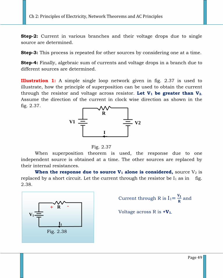
Ch 2: Principles of Electricity, Network Theorems and AC Principles
Page 49
R
V1
V2
I
Fig. 2.37
R
V1
I1
- +
Fig. 2.38
R
V1
V2
I
Step-2: Current in various branches and their voltage drops due to single
source are determined.
Step-3: This process is repeated for other sources by considering one at a time.
Step-4: Finally, algebraic sum of currents and voltage drops in a branch due to
different sources are determined.
Illustration 1: A simple single loop network given in fig. 2.37 is used to
illustrate, how the principle of superposition can be used to obtain the current
through the resistor and voltage across resistor. Let V1 be greater than V2.
Assume the direction of the current in clock wise direction as shown in the
fig. 2.37.
Fig. 2.37
When superposition theorem is used, the response due to one
independent source is obtained at a time. The other sources are replaced by
their internal resistances.
When the response due to source V1 alone is considered, source V2 is
replaced by a short circuit. Let the current through the resistor be I1 as in fig.
2.38.
Current through R is I1
and
Voltage across R is +V1.
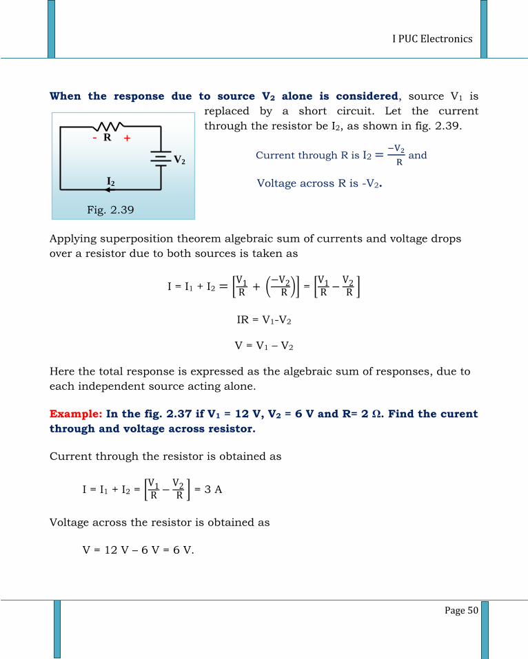
I PUC Electronics
Page 50
R
V2
I2
- +
Fig. 2.39
When the response due to source V2 alone is considered, source V1 is
replaced by a short circuit. Let the current
through the resistor be I2, as shown in fig. 2.39.
Current through R is I2
and
Voltage across R is -V2.
Applying superposition theorem algebraic sum of currents and voltage drops
over a resistor due to both sources is taken as
I = I1 + I2 [
(
)] = [
]
IR = V1-V2
V = V1 – V2
Here the total response is expressed as the algebraic sum of responses, due to
each independent source acting alone.
Example: In the fig. 2.37 if V1 = 12 V, V2 = 6 V and R= 2 Ω. Find the curent
through and voltage across resistor.
Current through the resistor is obtained as
I = I1 + I2 = [
] = 3 A
Voltage across the resistor is obtained as
V = 12 V – 6 V = 6 V.
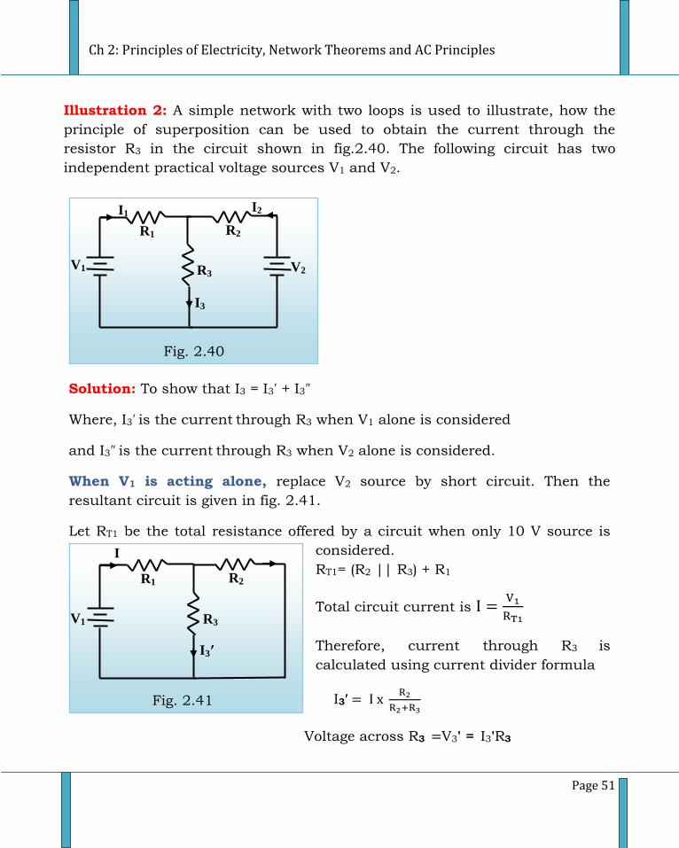
Ch 2: Principles of Electricity, Network Theorems and AC Principles
Page 51
R1
R3
V1
R2
V2
I3
I1 I2
Fig. 2.40
Illustration 2: A simple network with two loops is used to illustrate, how the
principle of superposition can be used to obtain the current through the
resistor R3 in the circuit shown in fig.2.40. The following circuit has two
independent practical voltage sources V1 and V2.
Solution: To show that I3 = I3′ + I3″
Where, I3′ is the current through R3 when V1 alone is considered
and I3″ is the current through R3 when V2 alone is considered.
When V1 is acting alone, replace V2 source by short circuit. Then the
resultant circuit is given in fig. 2.41.
Let RT1 be the total resistance offered by a circuit when only 10 V source is
considered.
RT1= (R2 || R3) + R1
Total circuit current is
Therefore, current through R3 is
calculated using current divider formula
I3′
Voltage across R3 V3' = I3'R3
R1
R3
V1
R2
I3′
I
Fig. 2.41
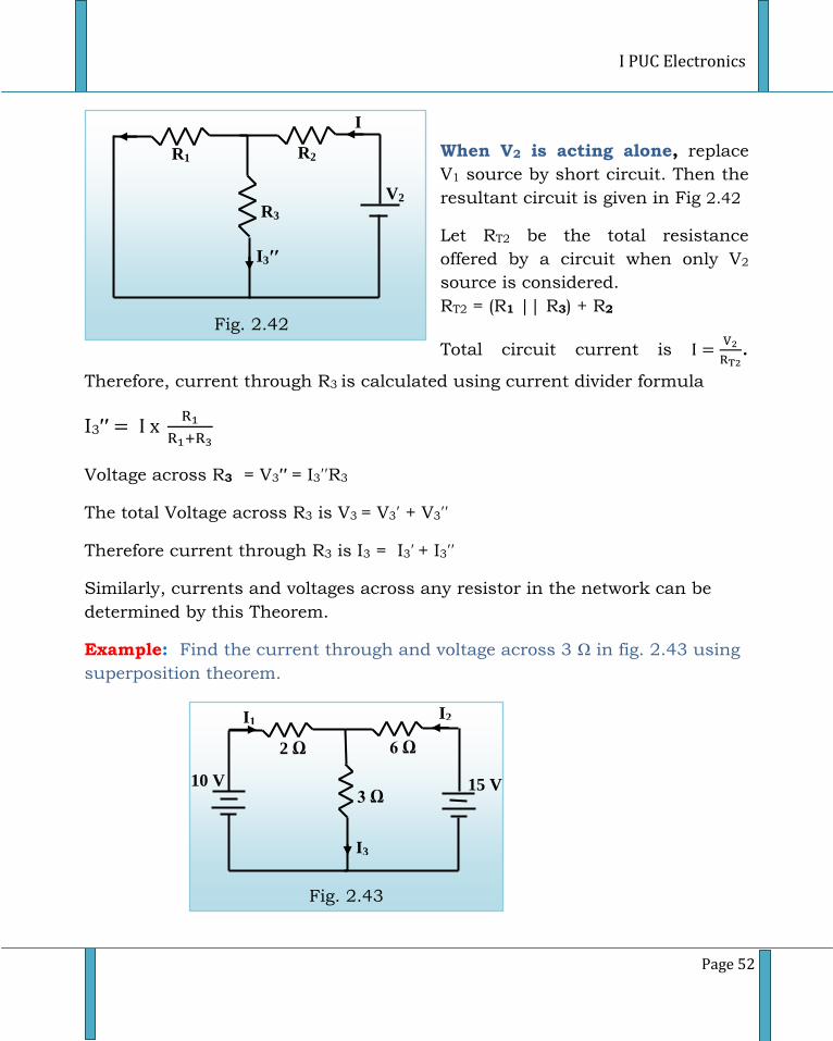
I PUC Electronics
Page 52
When V2 is acting alone, replace
V1 source by short circuit. Then the
resultant circuit is given in Fig 2.42
Let RT2 be the total resistance
offered by a circuit when only V2
source is considered.
RT2 = (R1 || R3) + R2
Total circuit current is
.
Therefore, current through R3 is calculated using current divider formula
I3′′
Voltage across R3 = V3′′ = I3′′R3
The total Voltage across R3 is V3 = V3′ + V3′′
Therefore current through R3 is I3 = I3′ + I3′′
Similarly, currents and voltages across any resistor in the network can be
determined by this Theorem.
Example: Find the current through and voltage across 3 Ω in fig. 2.43 using
superposition theorem.
2 Ω
3 Ω
6 Ω
15 V
I3
I1 I2
10 V
Fig. 2.43
R1
R3
R2
I3′′
V2
I
Fig. 2.42
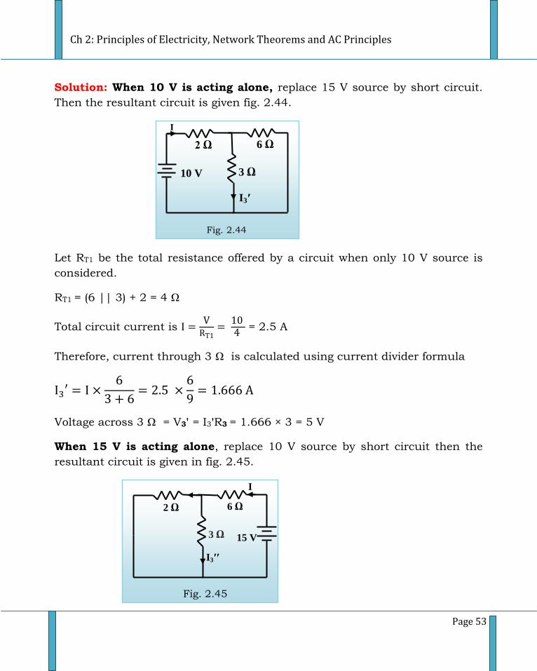
Ch 2: Principles of Electricity, Network Theorems and AC Principles
Page 53
Solution: When 10 V is acting alone, replace 15 V source by short circuit.
Then the resultant circuit is given fig. 2.44.
Let RT1 be the total resistance offered by a circuit when only 10 V source is
considered.
RT1 = (6 || 3) + 2 = 4 Ω
Total circuit current is
= 2.5 A
Therefore, current through 3 Ω is calculated using current divider formula
Voltage across 3 Ω = V3' = I3'R3 = 1.666 × 3 = 5 V
When 15 V is acting alone, replace 10 V source by short circuit then the
resultant circuit is given in fig. 2.45.
2 Ω
3 Ω
6 Ω
15 V
I
I3′′
Fig. 2.45
2 Ω
3 Ω
10 V
6 Ω
I
I3′
Fig. 2.44
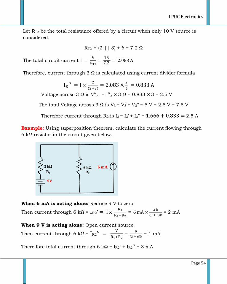
I PUC Electronics
Page 54
Let RT2 be the total resistance offered by a circuit when only 10 V source is
considered.
RT2 = (2 || 3) + 6 = 7.2 Ω
The total circuit current
Therefore, current through 3 Ω is calculated using current divider formula
( )
Voltage across 3 Ω is = 3 Ω = 0.833
3 = 2.5 V
The total Voltage across 3 Ω is V3 = V3′+ V3'' = 5 V + 2.5 V = 7.5 V
Therefore current through R2 is I3 = I3' + I3′′ = 2.5 A
Example: Using superposition theorem, calculate the current flowing through
6 kΩ resistor in the circuit given below.
When 6 mA is acting alone: Reduce 9 V to zero.
Then current through 6 kΩ = IR2′
=
( ) = 2 mA
When 9 V is acting alone: Open current source.
Then current through 6 kΩ = IR2
=
( ) = 1 mA
There fore total current through 6 kΩ = IR2′ + IR2 = 3 mA
6 kΩ 6 mA 3 kΩ
9V
R1 R2
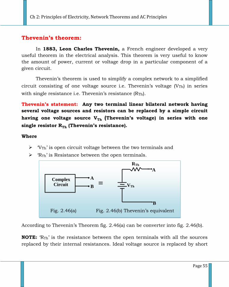
Ch 2: Principles of Electricity, Network Theorems and AC Principles
Page 55
Thevenin’s theorem:
In 1883, Leon Charles Thevenin, a French engineer developed a very
useful theorem in the electrical analysis. This theorem is very useful to know
the amount of power, current or voltage drop in a particular component of a
given circuit.
Thevenin’s theorem is used to simplify a complex network to a simplified
circuit consisting of one voltage source i.e. Thevenin’s voltage (VTh) in series
with single resistance i.e. Thevenin’s resistance (RTh).
Thevenin’s statement: Any two terminal linear bilateral network having
several voltage sources and resistors can be replaced by a simple circuit
having one voltage source VTh (Thevenin’s voltage) in series with one
single resistor RTh (Thevenin’s resistance).
Where
‘VTh’ is open circuit voltage between the two terminals and
‘RTh’ is Resistance between the open terminals.
According to Thevenin’s Theorem fig. 2.46(a) can be converter into fig. 2.46(b).
NOTE: ‘RTh’ is the resistance between the open terminals with all the sources
replaced by their internal resistances. Ideal voltage source is replaced by short
Fig. 2.46(a) Fig. 2.46(b) Thevenin’s equivalent
circuit
= Complex Circuit
A
B
RTh
VTh
A
B
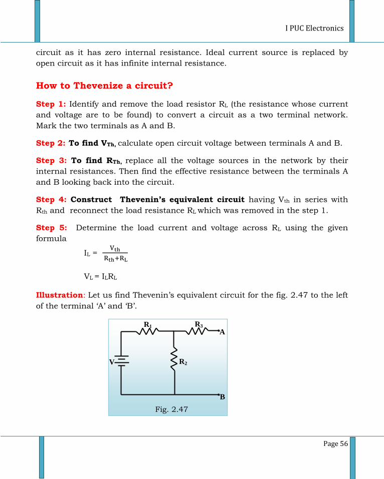
I PUC Electronics
Page 56
circuit as it has zero internal resistance. Ideal current source is replaced by
open circuit as it has infinite internal resistance.
How to Thevenize a circuit?
Step 1: Identify and remove the load resistor RL (the resistance whose current
and voltage are to be found) to convert a circuit as a two terminal network.
Mark the two terminals as A and B.
Step 2: To find VTh, calculate open circuit voltage between terminals A and B.
Step 3: To find RTh, replace all the voltage sources in the network by their
internal resistances. Then find the effective resistance between the terminals A
and B looking back into the circuit.
Step 4: Construct Thevenin’s equivalent circuit having Vth in series with
Rth and reconnect the load resistance RL which was removed in the step 1.
Step 5: Determine the load current and voltage across RL using the given
formula
IL =
VL = ILRL
Illustration: Let us find Thevenin’s equivalent circuit for the fig. 2.47 to the left
of the terminal ‘A’ and ‘B’.
R2
R1
V
R3
A
B
Fig. 2.47
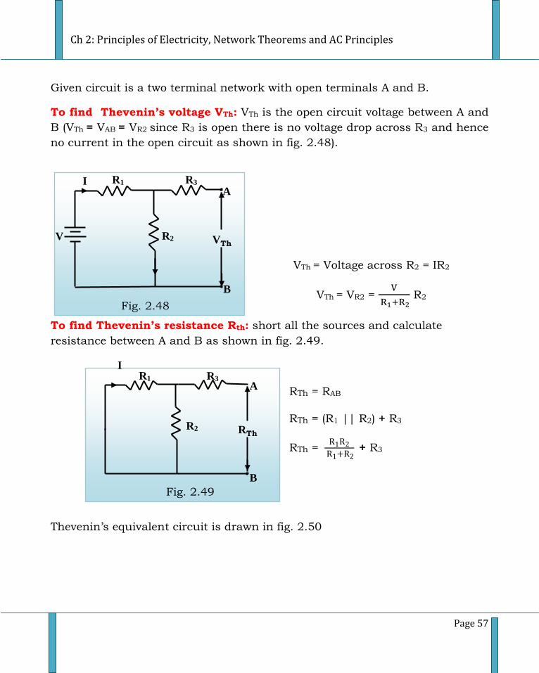
Ch 2: Principles of Electricity, Network Theorems and AC Principles
Page 57
Given circuit is a two terminal network with open terminals A and B.
To find Thevenin’s voltage VTh: VTh is the open circuit voltage between A and
B (VTh = VAB = VR2 since R3 is open there is no voltage drop across R3 and hence
no current in the open circuit as shown in fig. 2.48).
VTh = Voltage across R2 = IR2
VTh = VR2 =
R2
To find Thevenin’s resistance Rth: short all the sources and calculate
resistance between A and B as shown in fig. 2.49.
RTh = RAB
RTh = (R1 || R2) + R3
RTh =
+ R3
Thevenin’s equivalent circuit is drawn in fig. 2.50
R2
R1 R3 A
B
RTh
Fig. 2.49
I
R2
R1
V
R3
A
B
VTh
Fig. 2.48
I
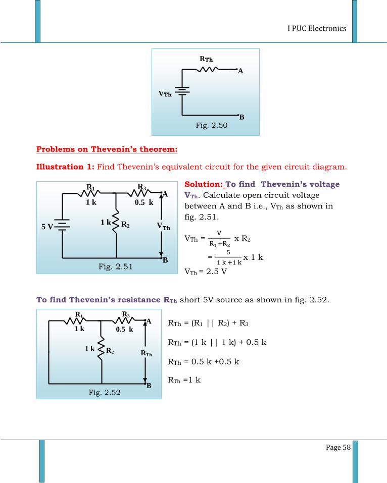
I PUC Electronics
Page 58
Problems on Thevenin’s theorem:
Illustration 1: Find Thevenin’s equivalent circuit for the given circuit diagram.
Solution: To find Thevenin’s voltage
VTh. Calculate open circuit voltage
between A and B i.e., VTh as shown in
fig. 2.51.
VTh =
x R2
=
x 1 k
VTh = 2.5 V
To find Thevenin’s resistance RTh short 5V source as shown in fig. 2.52.
RTh = (R1 || R2) + R3
RTh = (1 k || 1 k) + 0.5 k
RTh = 0.5 k +0.5 k
RTh =1 k
A
B
VTh
Fig. 2.50
R2
R1
R3
1 k A
B
0.5 k
1 k RTh
Fig. 2.52
RTh
R2
R1
5 V
R3
1 k A
B
0.5 k
1 k VTh
Fig. 2.51
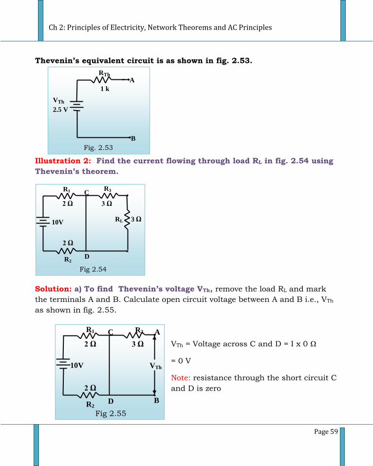
Ch 2: Principles of Electricity, Network Theorems and AC Principles
Page 59
Thevenin’s equivalent circuit is as shown in fig. 2.53.
Illustration 2: Find the current flowing through load RL in fig. 2.54 using
Thevenin’s theorem.
Solution: a) To find Thevenin’s voltage VTh, remove the load RL and mark
the terminals A and B. Calculate open circuit voltage between A and B i.e., VTh
as shown in fig. 2.55.
VTh = Voltage across C and D = I x 0 Ω
= 0 V
Note: resistance through the short circuit C
and D is zero
2 Ω 3 Ω
2 Ω
R1
10V
R3
R2
C
D
RL 3 Ω
Fig 2.54
RTh
1 k
A
B
VTh
2.5 V
Fig. 2.53
2 Ω 3 Ω
2 Ω
R1
R3 A
B R2
C
D
VTh 10V
Fig 2.55
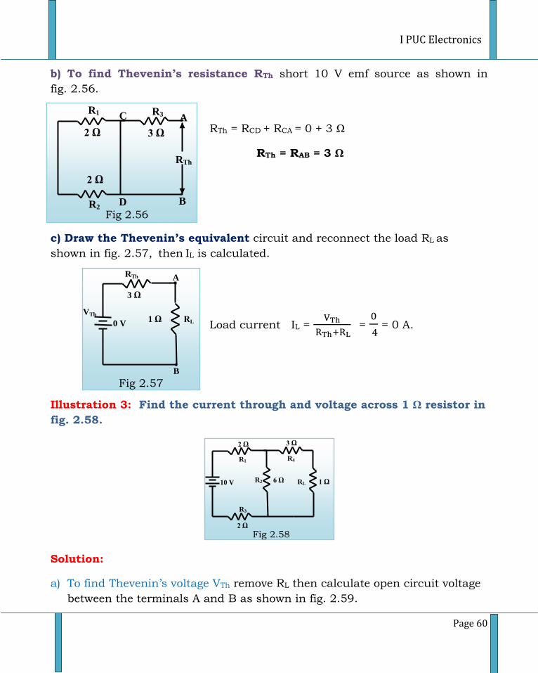
I PUC Electronics
Page 60
b) To find Thevenin’s resistance RTh short 10 V emf source as shown in
fig. 2.56.
RTh = RCD + RCA = 0 + 3 Ω
RTh = RAB = 3 Ω
c) Draw the Thevenin’s equivalent circuit and reconnect the load RL as
shown in fig. 2.57, then IL is calculated.
Load current IL =
=
= 0 A.
Illustration 3: Find the current through and voltage across 1 Ω resistor in
fig. 2.58.
Solution:
a) To find Thevenin’s voltage VTh remove RL then calculate open circuit voltage
between the terminals A and B as shown in fig. 2.59.
2 Ω 3 Ω
6 Ω
2 Ω
R1
10 V
R4
R2 RL 1 Ω
R3
Fig 2.58
(Short circuit)
R1
R3 A
B R2
RTh
C
D
2 Ω
2 Ω
3 Ω
Fig 2.56
RTh
3 Ω
VTh
A
B
0 V 1 Ω RL
Fig 2.57
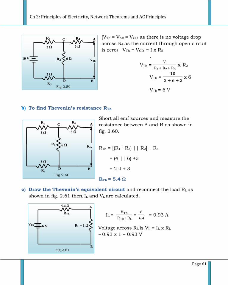
Ch 2: Principles of Electricity, Network Theorems and AC Principles
Page 61
(VTh = VAB = VCD as there is no voltage drop
across R4 as the current through open circuit
is zero) VTh = VCD = I x R2
.
VTh =
x R2
VTh =
x 6
VTh = 6 V
b) To find Thevenin’s resistance RTh
Short all emf sources and measure the
resistance between A and B as shown in
fig. 2.60.
RTh = [(R1+ R3) || R2] + R4
= (4 || 6) +3
= 2.4 + 3
RTh = 5.4 Ω
c) Draw the Thevenin’s equivalent circuit and reconnect the load RL as
shown in fig. 2.61 then. IL and VL are calculated.
IL =
=
= 0.93 A
Voltage across RL is VL = IL x RL
= 0.93 x 1 = 0.93 V
5.4 Ω
6 V
RTh
h
RL = 1 Ω VTh
A
B Fig 2.61
2 Ω 3 Ω
6 Ω
2 Ω
10 V
R4
R2 VTh
A
B D
C
R3 Fig 2.59
2 Ω 3 Ω
6 Ω
2 Ω
R1
R4
R2 Rth
A
B D
C
R3 Fig 2.60
R1
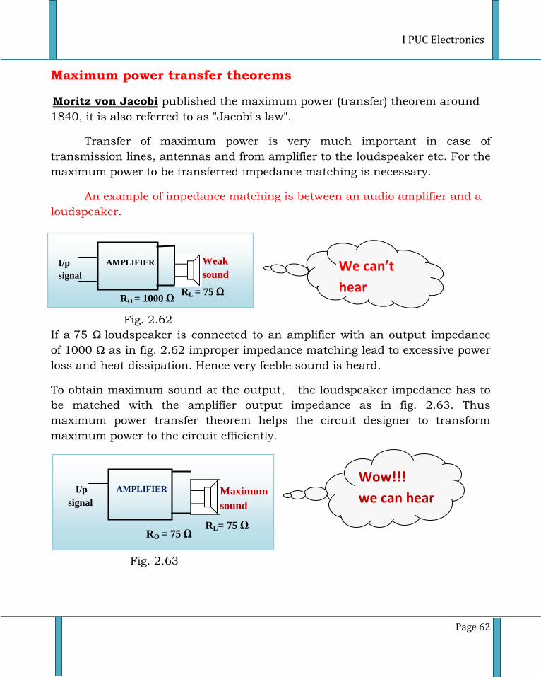
I PUC Electronics
Page 62
AMPLIFIER
RL = 75 Ω
I/p
signal
RO = 1000 Ω
Weak
sound
AMPLIFIER
RL= 75 Ω
I/p
signal
RO = 75 Ω
Maximum
sound
Fig 2.62
Fig 2.63
Maximum power transfer theorems
Moritz von Jacobi published the maximum power (transfer) theorem around
1840, it is also referred to as "Jacobi's law".
Transfer of maximum power is very much important in case of
transmission lines, antennas and from amplifier to the loudspeaker etc. For the
maximum power to be transferred impedance matching is necessary.
An example of impedance matching is between an audio amplifier and a
loudspeaker.
Fig. 2.62
If a 75 Ω loudspeaker is connected to an amplifier with an output impedance
of 1000 Ω as in fig. 2.62 improper impedance matching lead to excessive power
loss and heat dissipation. Hence very feeble sound is heard.
To obtain maximum sound at the output, the loudspeaker impedance has to
be matched with the amplifier output impedance as in fig. 2.63. Thus
maximum power transfer theorem helps the circuit designer to transform
maximum power to the circuit efficiently.
Fig. 2.63
Wow!!!
we can hear
We can’t
hear
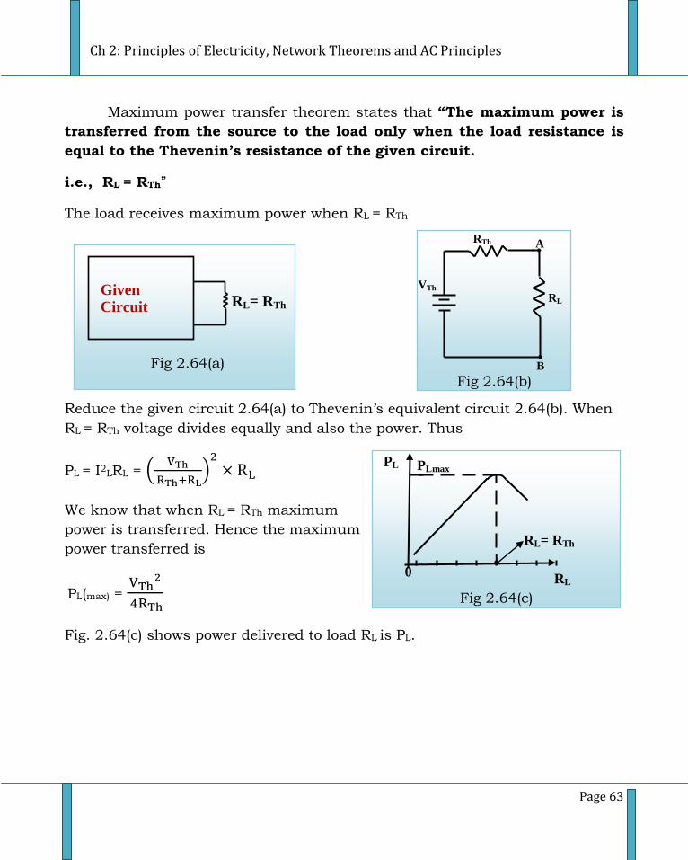
Ch 2: Principles of Electricity, Network Theorems and AC Principles
Page 63
Given Circuit RL= RTh
Fig 2.64(a)
0 RL
PL PLmax
RL= RTh
Fig 2.64(c)
Maximum power transfer theorem states that “The maximum power is
transferred from the source to the load only when the load resistance is
equal to the Thevenin’s resistance of the given circuit.
i.e., RL = RTh”
The load receives maximum power when RL = RTh
Reduce the given circuit 2.64(a) to Thevenin’s equivalent circuit 2.64(b). When
RL = RTh voltage divides equally and also the power. Thus
PL = I2LRL = (
)
We know that when RL = RTh maximum
power is transferred. Hence the maximum
power transferred is
PL(max) =
Fig. 2.64(c) shows power delivered to load RL is PL.
RTh
VTh
A
B
RL
Fig 2.64(b)
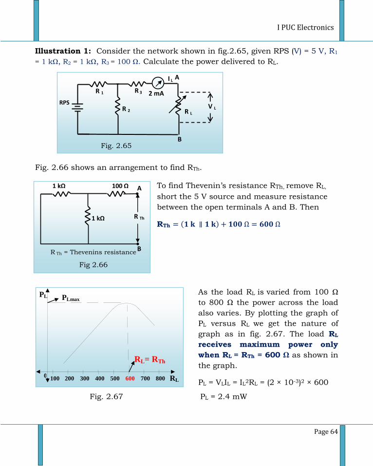
I PUC Electronics
Page 64
Fig 2.65
Illustration 1: Consider the network shown in fig.2.65, given RPS (V) = 5 V, R1
= 1 kΩ, R2 = 1 kΩ, R3 = 100 Ω. Calculate the power delivered to RL.
Fig. 2.66 shows an arrangement to find RTh.
To find Thevenin’s resistance RTh, remove RL,
short the 5 V source and measure resistance
between the open terminals A and B. Then
RTh ( )
As the load RL is varied from 100 Ω
to 800 Ω the power across the load
also varies. By plotting the graph of
PL versus RL we get the nature of
graph as in fig. 2.67. The load RL
receives maximum power only
when RL = RTh = 600 Ω as shown in
the graph.
PL = VLIL = IL2RL = (2 × 10⁻³)2 × 600
Fig. 2.67 PL = 2.4 mW
0 100 200 300 400 500 600 700 800
RL= RTh
RL
Ω
PLmax PL
R 1
R 2
R 3
A
B
RPS
V
Fig. 2.65
R L
V L
2 mA
I L
100 Ω 1 kΩ
1 kΩ
R Th = Thevenins resistance
R Th
Fig 2.66
A
B
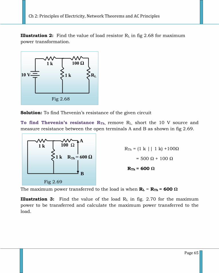
Ch 2: Principles of Electricity, Network Theorems and AC Principles
Page 65
100 Ω 1 k
1 k RTh = 600 Ω
A
B
Fig 2.69
Illustration 2: Find the value of load resistor RL in fig 2.68 for maximum
power transformation.
Solution: To find Thevenin’s resistance of the given circuit
To find Thevenin’s resistance RTh, remove RL, short the 10 V source and
measure resistance between the open terminals A and B as shown in fig 2.69.
RTh = (1 k || 1 k) +100Ω
= 500 Ω + 100 Ω
RTh = 600 Ω
The maximum power transferred to the load is when RL = RTh = 600 Ω
Illustration 3: Find the value of the load RL in fig. 2.70 for the maximum
power to be transferred and calculate the maximum power transferred to the
load.
100 Ω
10 V
1 k
RL 1 k
Fig 2.68
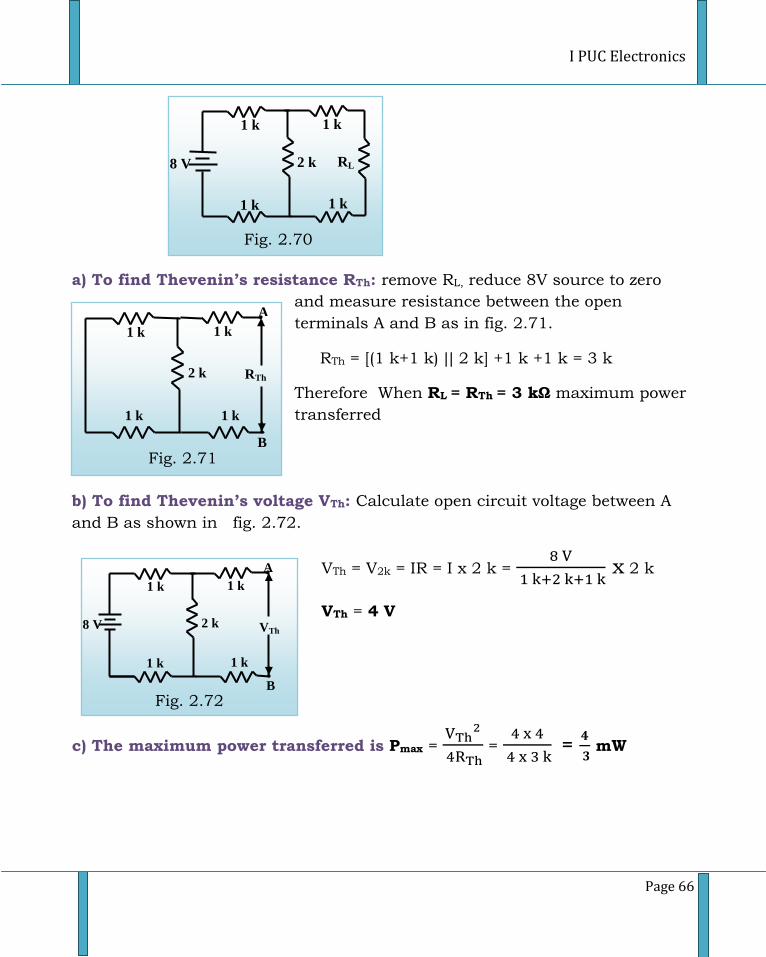
I PUC Electronics
Page 66
1 k
2 k
1 k
1 k
1 k
RTh
A
B Fig. 2.71
a) To find Thevenin’s resistance RTh: remove RL, reduce 8V source to zero
and measure resistance between the open
terminals A and B as in fig. 2.71.
RTh = [(1 k+1 k) 2 k] +1 k +1 k = 3 k
Therefore When RL = RTh = 3 kΩ maximum power
transferred
b) To find Thevenin’s voltage VTh: Calculate open circuit voltage between A
and B as shown in fig. 2.72.
VTh = V2k = IR = I x 2 k =
x 2 k
VTh = 4 V
c) The maximum power transferred is Pmax =
=
=
mW
1 k
2 k
1 k
8 V
1 k
RL
1 k
Fig. 2.70
1 k
2 k
1 k
1 k
VTh
A
B
8 V
1 k
Fig. 2.72
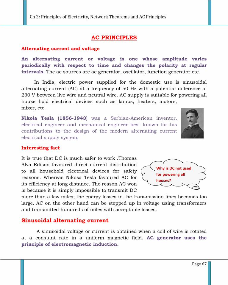
Ch 2: Principles of Electricity, Network Theorems and AC Principles
Page 67
AC PRINCIPLES
Alternating current and voltage
An alternating current or voltage is one whose amplitude varies
periodically with respect to time and changes the polarity at regular
intervals. The ac sources are ac generator, oscillator, function generator etc.
In India, electric power supplied for the domestic use is sinusoidal
alternating current (AC) at a frequency of 50 Hz with a potential difference of
230 V between live wire and neutral wire. AC supply is suitable for powering all
house hold electrical devices such as lamps, heaters, motors,
mixer, etc.
Nikola Tesla (1856-1943) was a Serbian-American inventor,
electrical engineer and mechanical engineer best known for his
contributions to the design of the modern alternating current
electrical supply system.
Interesting fact
It is true that DC is much safer to work .Thomas
Alva Edison favoured direct current distribution
to all household electrical devices for safety
reasons. Whereas Nikosa Tesla favoured AC for
its efficiency at long distance. The reason AC won
is because it is simply impossible to transmit DC
more than a few miles; the energy losses in the transmission lines becomes too
large. AC on the other hand can be stepped up in voltage using transformers
and transmitted hundreds of miles with acceptable losses.
Sinusoidal alternating current
A sinusoidal voltage or current is obtained when a coil of wire is rotated
at a constant rate in a uniform magnetic field. AC generator uses the
principle of electromagnetic induction.
Why is DC not used
for powering all
houses?
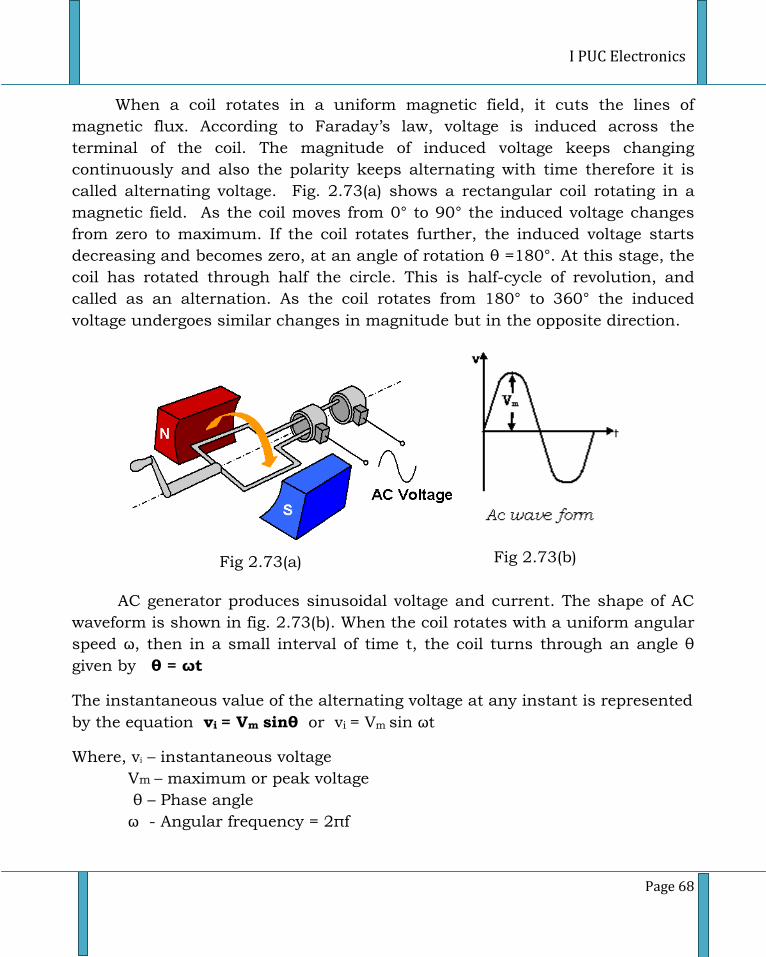
I PUC Electronics
Page 68
Fig 2.73(a) Fig 2.73(b)
When a coil rotates in a uniform magnetic field, it cuts the lines of
magnetic flux. According to Faraday’s law, voltage is induced across the
terminal of the coil. The magnitude of induced voltage keeps changing
continuously and also the polarity keeps alternating with time therefore it is
called alternating voltage. Fig. 2.73(a) shows a rectangular coil rotating in a
magnetic field. As the coil moves from 0° to 90° the induced voltage changes
from zero to maximum. If the coil rotates further, the induced voltage starts
decreasing and becomes zero, at an angle of rotation θ =180°. At this stage, the
coil has rotated through half the circle. This is half-cycle of revolution, and
called as an alternation. As the coil rotates from 180° to 360° the induced
voltage undergoes similar changes in magnitude but in the opposite direction.
AC generator produces sinusoidal voltage and current. The shape of AC
waveform is shown in fig. 2.73(b). When the coil rotates with a uniform angular
speed ω, then in a small interval of time t, the coil turns through an angle θ
given by θ = ωt
The instantaneous value of the alternating voltage at any instant is represented
by the equation vi = Vm sinθ or vi = Vm sin ωt
Where, vi – instantaneous voltage
Vm – maximum or peak voltage
θ – Phase angle
ω - Angular frequency = 2πf
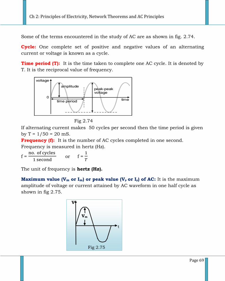
Ch 2: Principles of Electricity, Network Theorems and AC Principles
Page 69
Fig 2.74
Some of the terms encountered in the study of AC are as shown in fig. 2.74.
Cycle: One complete set of positive and negative values of an alternating
current or voltage is known as a cycle.
Time period (T): It is the time taken to complete one AC cycle. It is denoted by
T. It is the reciprocal value of frequency.
If alternating current makes 50 cycles per second then the time period is given
by T = 1/50 = 20 mS.
Frequency (f): It is the number of AC cycles completed in one second.
Frequency is measured in hertz (Hz).
f =
or f =
The unit of frequency is hertz (Hz).
Maximum value (Vm or Im) or peak value (Vp or Ip) of AC: It is the maximum
amplitude of voltage or current attained by AC waveform in one half cycle as
shown in fig 2.75.
Vm
t
max
V
Fig 2.75
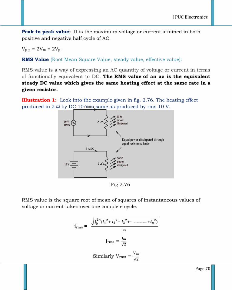
I PUC Electronics
Page 70
Fig 2.76
Peak to peak value: It is the maximum voltage or current attained in both
positive and negative half cycle of AC.
Vp-p = 2Vm = 2Vp.
RMS Value (Root Mean Square Value, steady value, effective value):
RMS value is a way of expressing an AC quantity of voltage or current in terms
of functionally equivalent to DC. The RMS value of an ac is the equivalent
steady DC value which gives the same heating effect at the same rate in a
given resistor.
Illustration 1: Look into the example given in fig. 2.76. The heating effect
produced in 2 Ω by DC 10 V is same as produced by rms 10 V.
10 V
RMS
50 W
power
dissipated
5 A RMS
10 V
50 W
power
dissipated
5 A DC
2
Equal power dissiapeted through
equal resistance loads
2
RMS value is the square root of mean of squares of instantaneous values of
voltage or current taken over one complete cycle.
irms = √∫ (
)
Irms =
√
Similarly Vrms =
√
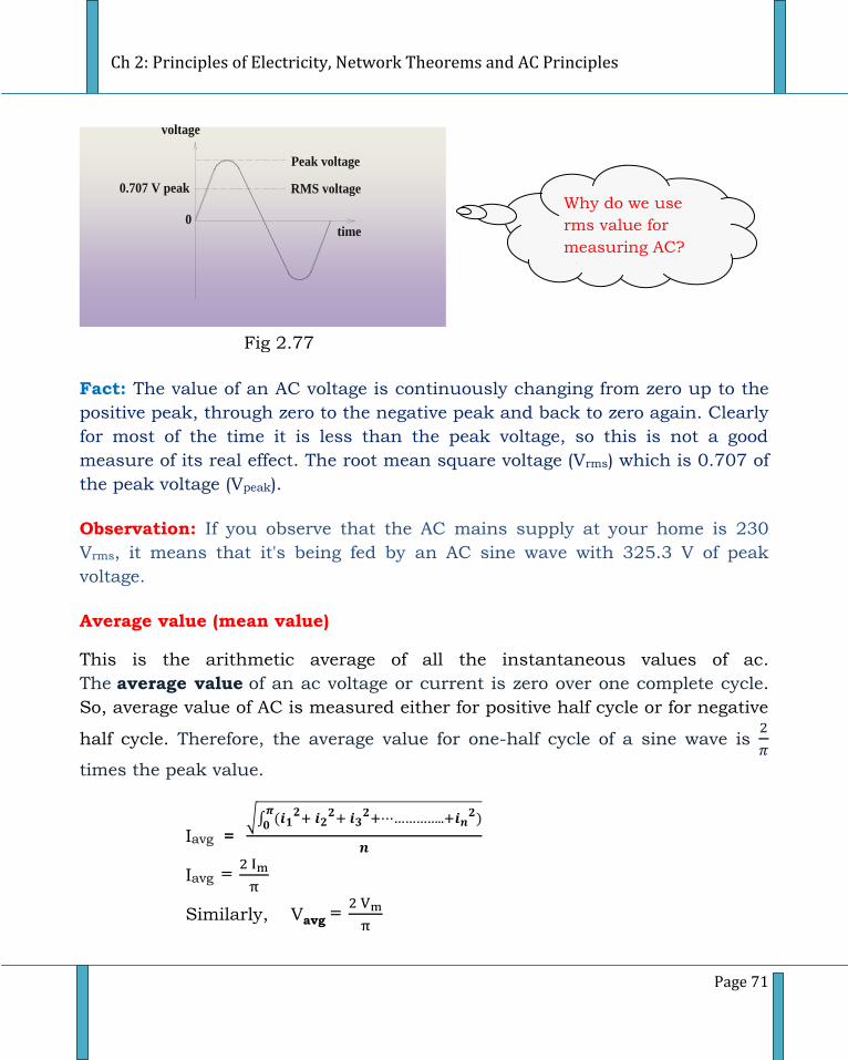
Ch 2: Principles of Electricity, Network Theorems and AC Principles
Page 71
Fig 2.77
voltage
0time
RMS voltage
Peak voltage
0.707 V peak
Fact: The value of an AC voltage is continuously changing from zero up to the
positive peak, through zero to the negative peak and back to zero again. Clearly
for most of the time it is less than the peak voltage, so this is not a good
measure of its real effect. The root mean square voltage (Vrms) which is 0.707 of
the peak voltage (Vpeak).
Observation: If you observe that the AC mains supply at your home is 230
Vrms, it means that it's being fed by an AC sine wave with 325.3 V of peak
voltage.
Average value (mean value)
This is the arithmetic average of all the instantaneous values of ac.
The average value of an ac voltage or current is zero over one complete cycle.
So, average value of AC is measured either for positive half cycle or for negative
half cycle. Therefore, the average value for one-half cycle of a sine wave is
times the peak value.
Iavg = √∫ (
)
Iavg =
Similarly, Vavg =
Why do we use
rms value for
measuring AC?
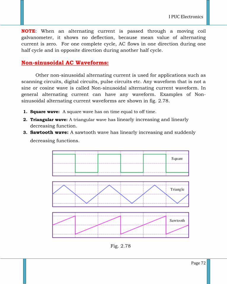
I PUC Electronics
Page 72
NOTE: When an alternating current is passed through a moving coil
galvanometer, it shows no deflection, because mean value of alternating
current is zero. For one complete cycle, AC flows in one direction during one
half cycle and in opposite direction during another half cycle.
Non-sinusoidal AC Waveforms:
Other non-sinusoidal alternating current is used for applications such as
scanning circuits, digital circuits, pulse circuits etc. Any waveform that is not a
sine or cosine wave is called Non-sinusoidal alternating current waveform. In
general alternating current can have any waveform. Examples of Non-
sinusoidal alternating current waveforms are shown in fig. 2.78.
1. Square wave: A square wave has on time equal to off time.
2. Triangular wave: A triangular wave has linearly increasing and linearly
decreasing function.
3. Sawtooth wave: A sawtooth wave has linearly increasing and suddenly
decreasing functions.
Fig. 2.78
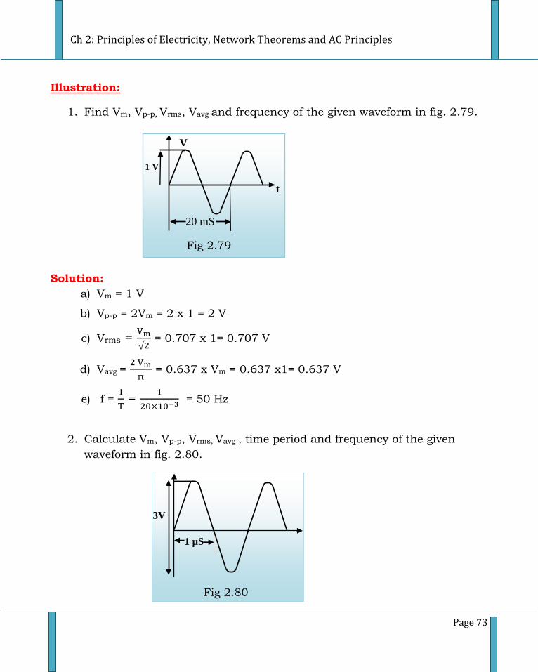
Ch 2: Principles of Electricity, Network Theorems and AC Principles
Page 73
Illustration:
1. Find Vm, Vp-p, Vrms, Vavg and frequency of the given waveform in fig. 2.79.
Solution:
a) Vm = 1 V
b) Vp-p = 2Vm = 2 x 1 = 2 V
c) Vrms =
√ = 0.707 x 1= 0.707 V
d) Vavg =
π = 0.637 x Vm = 0.637 x1= 0.637 V
e) f =
=
= 50 Hz
2. Calculate Vm, Vp-p, Vrms, Vavg , time period and frequency of the given
waveform in fig. 2.80.
3V
1 µS
S
µ Fig 2.80
1 V
20 mS
t
V
Fig 2.79
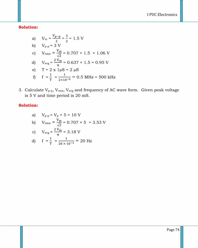
I PUC Electronics
Page 74
Solution:
a) Vm =
=
= 1.5 V
b) Vp-p = 3 V
c) Vrms =
√ = 0.707 × 1.5 = 1.06 V
d) Vavg =
= 0.637 × 1.5 = 0.95 V
e) T = 2 x 1µS = 2 µS
f) f =
=
= 0.5 MHz = 500 kHz
3. Calculate Vp-p, Vrms, Vavg and frequency of AC wave form. Given peak voltage
is 5 V and time period is 20 mS.
Solution:
a) Vp-p = Vp × 5 = 10 V
b) Vrms =
√ = 0.707 × 5 = 3.53 V
c) Vavg =
= 3.18 V
d) f =
=
= 20 Hz
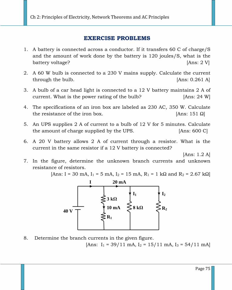
Ch 2: Principles of Electricity, Network Theorems and AC Principles
Page 75
EXERCISE PROBLEMS
1. A battery is connected across a conductor. If it transfers 60 C of charge/S
and the amount of work done by the battery is 120 joules/S, what is the
battery voltage? [Ans: 2 V]
2. A 60 W bulb is connected to a 230 V mains supply. Calculate the current
through the bulb. [Ans: 0.261 A]
3. A bulb of a car head light is connected to a 12 V battery maintains 2 A of
current. What is the power rating of the bulb? [Ans: 24 W]
4. The specifications of an iron box are labeled as 230 AC, 350 W. Calculate
the resistance of the iron box. [Ans: 151 Ω]
5. An UPS supplies 2 A of current to a bulb of 12 V for 5 minutes. Calculate
the amount of charge supplied by the UPS. [Ans: 600 C]
6. A 20 V battery allows 2 A of current through a resistor. What is the
current in the same resistor if a 12 V battery is connected?
[Ans: 1.2 A]
7. In the figure, determine the unknown branch currents and unknown
resistance of resistors.
[Ans: I = 30 mA, I1 = 5 mA, I2 = 15 mA, R1 = 1 kΩ and R2 = 2.67 kΩ]
8. Determine the branch currents in the given figure.
[Ans: I1 = 39/11 mA, I2 = 15/11 mA, I3 = 54/11 mA]
40 V
I 20 mA
I1 I2
10 mA
3 kΩ
R1
8 kΩ R2
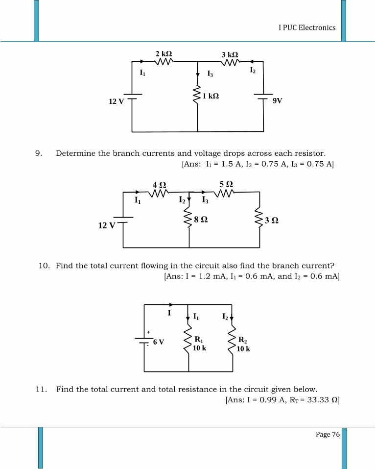
I PUC Electronics
Page 76
R1 R2 6 V
+
- 10 k 10 k
I I1 I2
9. Determine the branch currents and voltage drops across each resistor.
[Ans: I1 = 1.5 A, I2 = 0.75 A, I3 = 0.75 A]
10. Find the total current flowing in the circuit also find the branch current?
[Ans: I = 1.2 mA, I1 = 0.6 mA, and I2 = 0.6 mA]
11. Find the total current and total resistance in the circuit given below.
[Ans: I = 0.99 A, RT = 33.33 Ω]
12 V
4 Ω 5 Ω
8 Ω 3 Ω
I1 I3 I2
12 V
2 kΩ
1 kΩ 9V
3 kΩ
I3 I2 I1
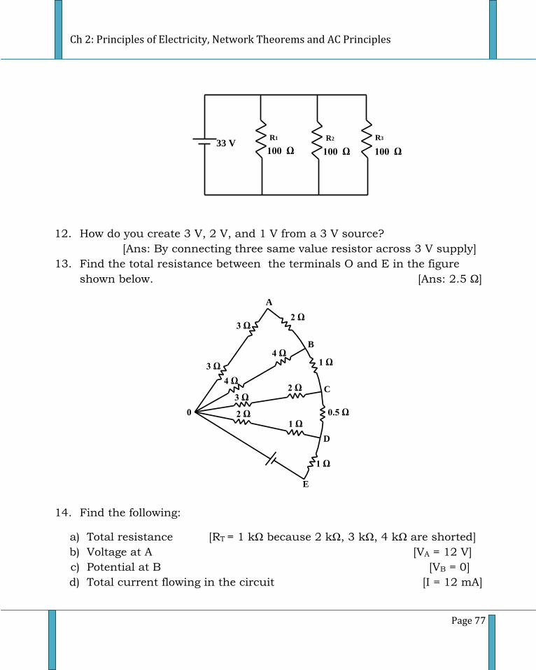
Ch 2: Principles of Electricity, Network Theorems and AC Principles
Page 77
R 1 R 2 33 V
R 3
100 Ω 100 Ω 100 Ω
12. How do you create 3 V, 2 V, and 1 V from a 3 V source?
[Ans: By connecting three same value resistor across 3 V supply]
13. Find the total resistance between the terminals O and E in the figure
shown below. [Ans: 2.5 Ω]
14. Find the following:
a) Total resistance [RT = 1 kΩ because 2 kΩ, 3 kΩ, 4 kΩ are shorted]
b) Voltage at A [VA = 12 V]
c) Potential at B [VB = 0]
d) Total current flowing in the circuit [I = 12 mA]
3 Ω
4 Ω
4 Ω
3 Ω 2 Ω
2 Ω 1 Ω
A
0.5 Ω
1 Ω
2 Ω
1 Ω
3 Ω
B
C
D
E
0
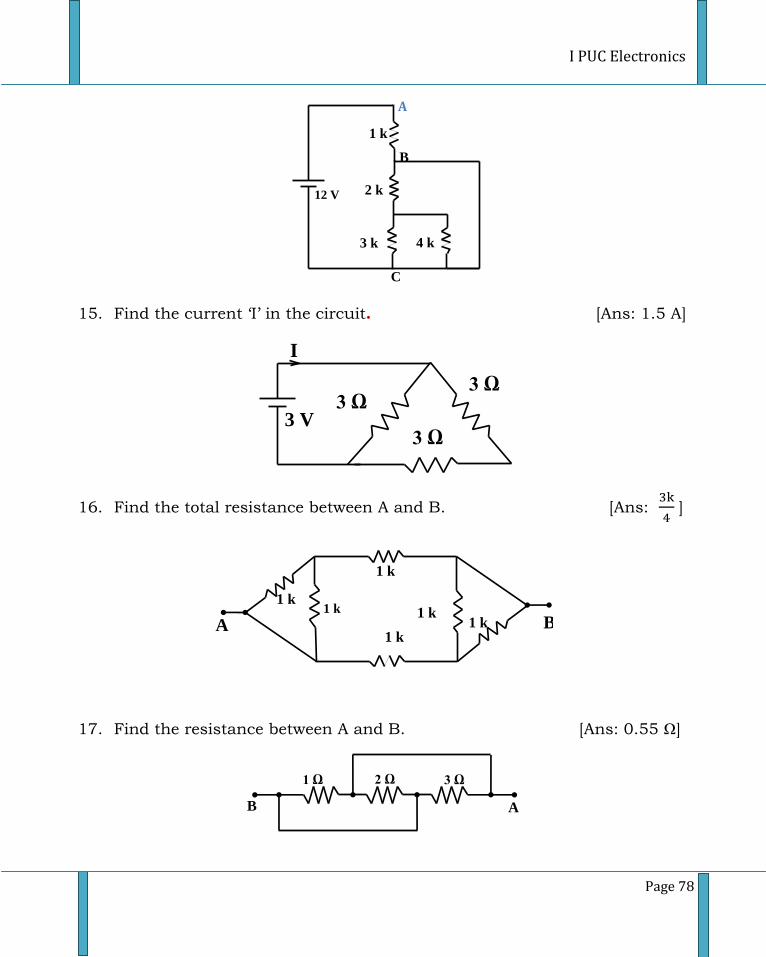
I PUC Electronics
Page 78
15. Find the current ‘I’ in the circuit. [Ans: 1.5 A]
16. Find the total resistance between A and B. [Ans:
]
17. Find the resistance between A and B. [Ans: 0.55 Ω]
2 Ω 3 Ω
A B
1 Ω
1 k
1 k
1 k 1 k 1 k
1 k
A B
3 Ω
I
3 V 3 Ω
3 Ω
1 k
12 V 2 k
3 k 4 k
B
C
A
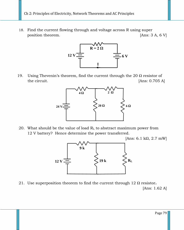
Ch 2: Principles of Electricity, Network Theorems and AC Principles
Page 79
R = 2 Ω
12 V
6 V
I
2 Ω
24 V
4 Ω
20 Ω 6 Ω
18. Find the current flowing through and voltage across R using super
position theorem. [Ans: 3 A, 6 V]
19. Using Thevenin’s theorem, find the current through the 20 Ω resistor of
the circuit. [Ans: 0.705 A]
20. What should be the value of load RL to abstract maximum power from
12 V battery? Hence determine the power transferred.
[Ans: 6.1 kΩ, 2.7 mW]
21. Use superposition theorem to find the current through 12 Ω resistor.
[Ans: 1.62 A]
12 V
9 k
RL 19 k
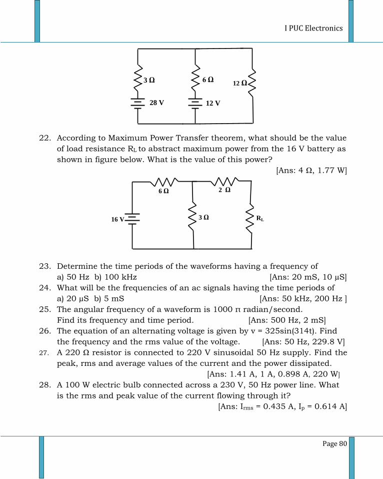
I PUC Electronics
Page 80
2 Ω
16 V
6 Ω
3 Ω RL
22. According to Maximum Power Transfer theorem, what should be the value
of load resistance RL to abstract maximum power from the 16 V battery as
shown in figure below. What is the value of this power?
[Ans: 4 Ω, 1.77 W]
23. Determine the time periods of the waveforms having a frequency of
a) 50 Hz b) 100 kHz [Ans: 20 mS, 10 µS]
24. What will be the frequencies of an ac signals having the time periods of
a) 20 µS b) 5 mS [Ans: 50 kHz, 200 Hz ]
25. The angular frequency of a waveform is 1000 π radian/second.
Find its frequency and time period. [Ans: 500 Hz, 2 mS]
26. The equation of an alternating voltage is given by v = 325sin(314t). Find
the frequency and the rms value of the voltage. [Ans: 50 Hz, 229.8 V]
27. A 220 Ω resistor is connected to 220 V sinusoidal 50 Hz supply. Find the
peak, rms and average values of the current and the power dissipated.
[Ans: 1.41 A, 1 A, 0.898 A, 220 W]
28. A 100 W electric bulb connected across a 230 V, 50 Hz power line. What
is the rms and peak value of the current flowing through it?
[Ans: Irms = 0.435 A, Ip = 0.614 A]
6 Ω
12 Ω 3 Ω
28 V 12 V
Ch 2: Principles of Electricity, Network Theorems and AC Principles
Page 81
29. A sinusoidal voltage varies from zero to a maximum value of 200 V. How
much is its value at the instances of
a) 300 b) 450 c) 900 d) 2700 ? [Ans: 100 V, 141.4 V, 200 V, -200 V]
30. If the peak value is 240 V, find out its effective value. [Vrms = 169.70 V]
Questions
One mark questions:
1. What is the unit of electric charge?
2. What is the magnitude of a charge?
3. Define potential difference.
4. Define electric current.
5. What is the unit of electric current?
6. What is the direction of conventional current?
7. What is the direction of electron current?
8. Define DC current.
9. Define ampere.
10. Give an example for DC source.
11. State Ohm’s law.
12. Is Ohm’s law applicable when the temperature of a conductor
continuously changes?
13. Is Ohm’s law applicable to semiconductors?
14. Is Ohm’s law applicable to insulators?
15. According to Ohm’s law how are ‘V’ and ‘I’ related?
16. What is the resistance of a conductor?
17. Mention the unit of resistance.
18. What is an electric power?
19. What is an electric energy?
20. Define voltage source.
21. Define current source.
22. What is a node?
23. What is a branch in a circuit?
I PUC Electronics
Page 82
24. What is a ‘loop’ in an electrical circuit?
25. What is a closed loop?
26. What is an open loop?
27. What is a mesh in a closed circuit?
28. What is meant by a linear network? Give an example.
29. What is meant by a nonlinear network? Give an example.
30. What is meant by unilateral network?
31. What is meant by bilateral network?
32. State KCL.
33. State KVL.
34. What is the commercial or Board Of Trade (BOT) unit of electrical energy?
35. Define kWh.
36. When will a load receives maximum power from a source?
37. Mention an application of maximum power transfer theorem.
38. How is the Thevenin’s resistance of a network determined?
39. How do you measure Thevenin’s voltage?
40. How do you measure Thevenin’s resistance?
41. How much is the AC voltage supplied to all household electrical devices in
India?
42. Mention the unit of frequency.
43. Write the relation between frequency and time period.
44. What is the relation between RMS value and peak value of AC?
45. Give an expression for instantaneous value of AC voltage.
Two marks questions:
46. Mention the types of electrical charge.
47. Mention any two properties of charges.
48. What is the difference between conventional current and electron current?
49. State and explain Ohm’s law.
50. Mention the limitations of Ohm’s law.
51. Briefly explain about electrical energy.
52. What are primary DC-sources? Give an example.
53. What are secondary DC-sources? Give an example.
54. Draw the circuit of a practical voltage source.
55. Draw the circuit of a practical current source.
Ch 2: Principles of Electricity, Network Theorems and AC Principles
Page 83
56. State Kirchhoff’s laws.
57. Draw the V-I characteristics of a practical voltage source.
58. Briefly explain the conversion of voltage source into current source.
59. What is series combination of resistors?
60. What is parallel combination of resistors?
61. State Thevenin’s theorem.
62. State Superposition theorem.
63. State maximum power transfer theorem.
64. Draw any two non sinusoidal waveforms.
65. Define frequency and time period. Write their relation.
66. Define peak value and RMS value.
Three/five marks questions:
67. Mention the properties of charges.
68. State and explain KCL.
69. State and explain KVL.
70. Explain how a voltage source is converted into its equivalent current
source.
71. Explain how a current source is converted into its equivalent voltage
source.
72. Distinguish between DC and AC current.
73. Derive an expression for the effective resistance of two resistors connected
in series.
74. Derive an expression for the effective resistance of two resistors connected
in parallel.
75. Explain voltage divider rule.
76. Explain current divider rule.
77. State and explain Thevenin’s theorem with an example.
78. State and explain maximum power transfer theorem with an example
79. Write the procedure to Thevenise a given circuit with an example.
80. State and explain superposition theorem.
81. Define the following terms. a) Cycle b) Frequency c) Time period
d) Peak value.
82. Write a note on AC generation.
I PUC Electronics
Page 84
83. Define the following terms in an AC signal
a) Frequency b) Time period c) Peak Value d) Instantaneous voltage
e) rms value.
84. Define the following terms with respect to an AC signal
a) Cycle b) Effective value c) Peak to peak value d) Average value.
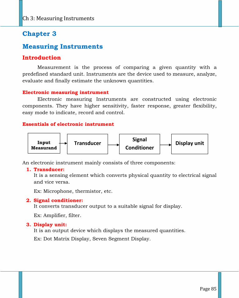
Ch 3: Measuring Instruments
Page 85
Chapter 3
Measuring Instruments
Introduction
Measurement is the process of comparing a given quantity with a
predefined standard unit. Instruments are the device used to measure, analyze,
evaluate and finally estimate the unknown quantities.
Electronic measuring instrument
Electronic measuring Instruments are constructed using electronic
components. They have higher sensitivity, faster response, greater flexibility,
easy mode to indicate, record and control.
Essentials of electronic instrument
An electronic instrument mainly consists of three components:
1. Transducer: It is a sensing element which converts physical quantity to electrical signal
and vice versa.
Ex: Microphone, thermistor, etc.
2. Signal conditioner: It converts transducer output to a suitable signal for display.
Ex: Amplifier, filter.
3. Display unit:
It is an output device which displays the measured quantities.
Ex: Dot Matrix Display, Seven Segment Display.
Transducer Signal
Conditioner Display unit Input
Measurand
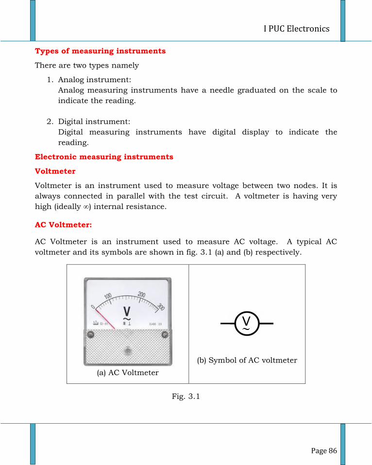
I PUC Electronics
Page 86
Types of measuring instruments
There are two types namely
1. Analog instrument:
Analog measuring instruments have a needle graduated on the scale to
indicate the reading.
2. Digital instrument:
Digital measuring instruments have digital display to indicate the
reading.
Electronic measuring instruments
Voltmeter
Voltmeter is an instrument used to measure voltage between two nodes. It is
always connected in parallel with the test circuit. A voltmeter is having very
high (ideally ∞) internal resistance.
AC Voltmeter:
AC Voltmeter is an instrument used to measure AC voltage. A typical AC
voltmeter and its symbols are shown in fig. 3.1 (a) and (b) respectively.
(a) AC Voltmeter
(b) Symbol of AC voltmeter
Fig. 3.1
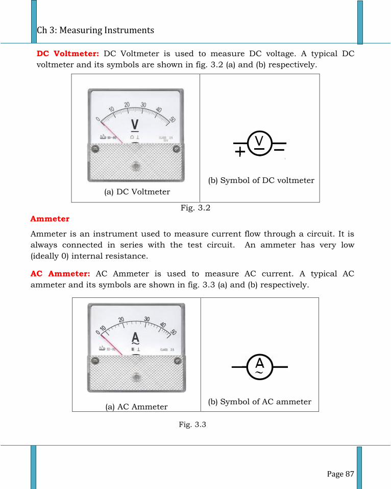
Ch 3: Measuring Instruments
Page 87
DC Voltmeter: DC Voltmeter is used to measure DC voltage. A typical DC
voltmeter and its symbols are shown in fig. 3.2 (a) and (b) respectively.
Fig. 3.2
Ammeter
Ammeter is an instrument used to measure current flow through a circuit. It is
always connected in series with the test circuit. An ammeter has very low
(ideally 0) internal resistance.
AC Ammeter: AC Ammeter is used to measure AC current. A typical AC
ammeter and its symbols are shown in fig. 3.3 (a) and (b) respectively.
(a) AC Ammeter
(b) Symbol of AC ammeter
Fig. 3.3
(a) DC Voltmeter
(b) Symbol of DC voltmeter
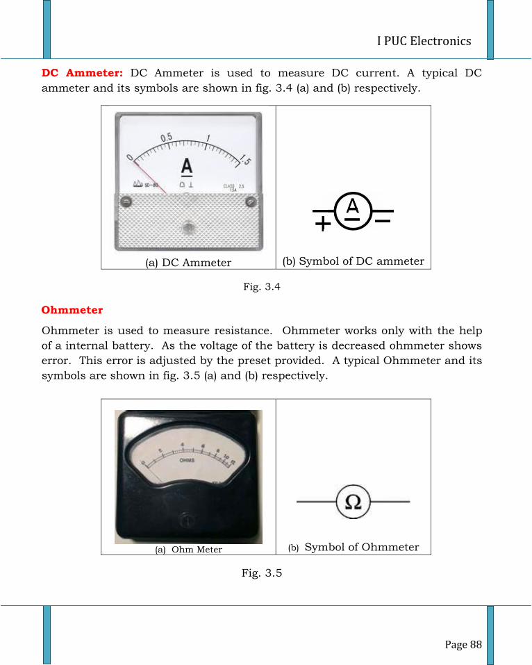
I PUC Electronics
Page 88
DC Ammeter: DC Ammeter is used to measure DC current. A typical DC
ammeter and its symbols are shown in fig. 3.4 (a) and (b) respectively.
(a) DC Ammeter
(b) Symbol of DC ammeter
Fig. 3.4
Ohmmeter
Ohmmeter is used to measure resistance. Ohmmeter works only with the help
of a internal battery. As the voltage of the battery is decreased ohmmeter shows
error. This error is adjusted by the preset provided. A typical Ohmmeter and its
symbols are shown in fig. 3.5 (a) and (b) respectively.
(a) Ohm Meter
(b) Symbol of Ohmmeter
Fig. 3.5
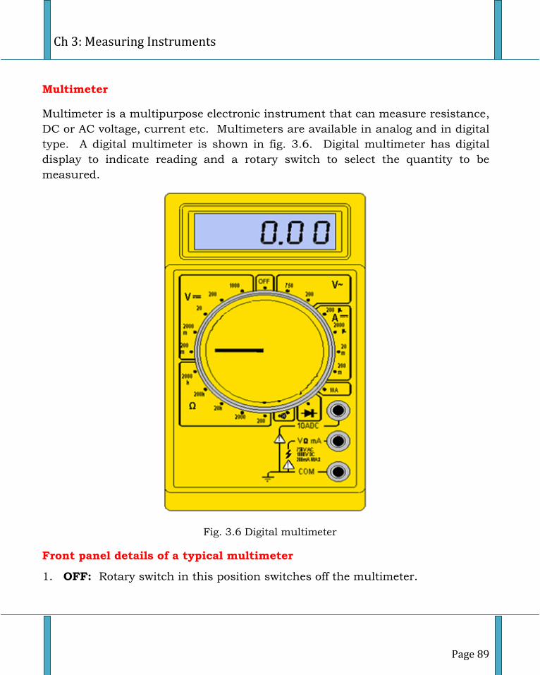
Ch 3: Measuring Instruments
Page 89
Multimeter
Multimeter is a multipurpose electronic instrument that can measure resistance,
DC or AC voltage, current etc. Multimeters are available in analog and in digital
type. A digital multimeter is shown in fig. 3.6. Digital multimeter has digital
display to indicate reading and a rotary switch to select the quantity to be
measured.
Fig. 3.6 Digital multimeter
Front panel details of a typical multimeter
1. OFF: Rotary switch in this position switches off the multimeter.
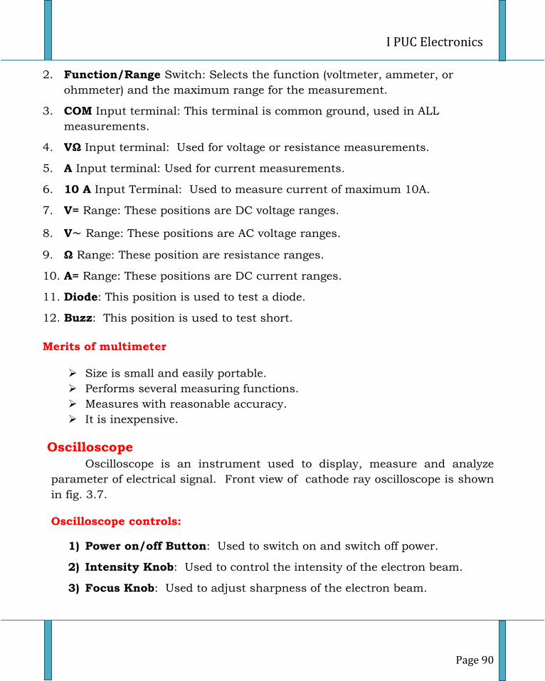
I PUC Electronics
Page 90
2. Function/Range Switch: Selects the function (voltmeter, ammeter, or
ohmmeter) and the maximum range for the measurement.
3. COM Input terminal: This terminal is common ground, used in ALL
measurements.
4. VΩ Input terminal: Used for voltage or resistance measurements.
5. A Input terminal: Used for current measurements.
6. 10 A Input Terminal: Used to measure current of maximum 10A.
7. V= Range: These positions are DC voltage ranges.
8. V Range: These positions are AC voltage ranges.
9. Ω Range: These position are resistance ranges.
10. A= Range: These positions are DC current ranges.
11. Diode: This position is used to test a diode.
12. Buzz: This position is used to test short.
Merits of multimeter
Size is small and easily portable.
Performs several measuring functions.
Measures with reasonable accuracy.
It is inexpensive.
Oscilloscope
Oscilloscope is an instrument used to display, measure and analyze
parameter of electrical signal. Front view of cathode ray oscilloscope is shown
in fig. 3.7.
Oscilloscope controls:
1) Power on/off Button: Used to switch on and switch off power.
2) Intensity Knob: Used to control the intensity of the electron beam.
3) Focus Knob: Used to adjust sharpness of the electron beam.
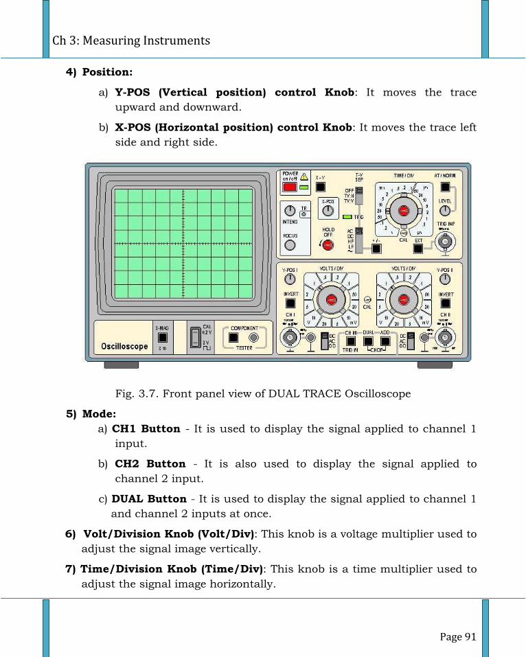
Ch 3: Measuring Instruments
Page 91
4) Position:
a) Y-POS (Vertical position) control Knob: It moves the trace
upward and downward.
b) X-POS (Horizontal position) control Knob: It moves the trace left
side and right side.
Fig. 3.7. Front panel view of DUAL TRACE Oscilloscope
5) Mode:
a) CH1 Button - It is used to display the signal applied to channel 1
input.
b) CH2 Button - It is also used to display the signal applied to
channel 2 input.
c) DUAL Button - It is used to display the signal applied to channel 1
and channel 2 inputs at once.
6) Volt/Division Knob (Volt/Div): This knob is a voltage multiplier used to
adjust the signal image vertically.
7) Time/Division Knob (Time/Div): This knob is a time multiplier used to
adjust the signal image horizontally.
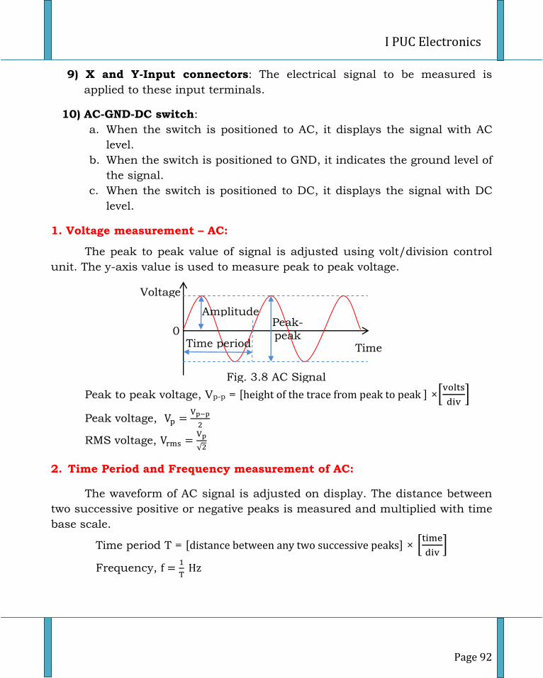
I PUC Electronics
Page 92
9) X and Y-Input connectors: The electrical signal to be measured is
applied to these input terminals.
10) AC-GND-DC switch:
a. When the switch is positioned to AC, it displays the signal with AC
level.
b. When the switch is positioned to GND, it indicates the ground level of
the signal.
c. When the switch is positioned to DC, it displays the signal with DC
level.
1. Voltage measurement – AC:
The peak to peak value of signal is adjusted using volt/division control
unit. The y-axis value is used to measure peak to peak voltage.
Peak to peak voltage, Vp-p = [ ] ×[
]
Peak voltage,
RMS voltage,
√
2. Time Period and Frequency measurement of AC:
The waveform of AC signal is adjusted on display. The distance between
two successive positive or negative peaks is measured and multiplied with time
base scale.
Time period T = [ ] × [
]
Frequency,
Voltage
Amplitude
Time period
Peak-peak
Voltage Time
0
Fig. 3.8 AC Signal
Ch 3: Measuring Instruments
Page 93
3. Voltage Measurement – DC:
1. Select any convenient time-base setting.
2. Keep AC-GND-DC switch to GND position.
3. Adjust the position so that the trace lies on centre line at GND.
4. Keep AC-GND-DC switch to DC position.
5. Connect DC voltage to channel input.
6. Trace line shifts upward or downward depending on polarity and signal
strength.
7. Take readings of the y-position of the trace and note the volts/div setting
8. DC voltage = [ ] × [
] setting.
Application of oscilloscope:
It is used to study the nature of waveform.
It is used to measure AC/DC voltage.
It is used to measure time, time period and frequency.
It is used to compare frequency and phase of input signals.
Precautions using electronic instruments
The following precautions are advised while using electronic instruments
1. Study user’s manual before using the instrument.
2. DC meters must be connected with proper polarity. 3. Ammeter must be connected in series with the circuit.
4. Voltmeter must be connected in parallel with the circuit.
5. Select proper range of meters for conducting experiment.
6. Don’t allow the current or voltage to the meters beyond the maximum
limit.
7. Completely switch off the circuit during connection or reconnection of
meters.
8. Use the multimeter by selecting proper range and function for quantities
to be measured like resistance, voltage AC/DC, current and also select
proper terminals (Com, VΩ, I).
9. Don’t try to solder or de-solder the circuit when the oscilloscope is
connected. Remove oscilloscope connections before soldering or de-
soldering.
10. Don’t apply high AC voltage (> 230 V) to oscilloscope.
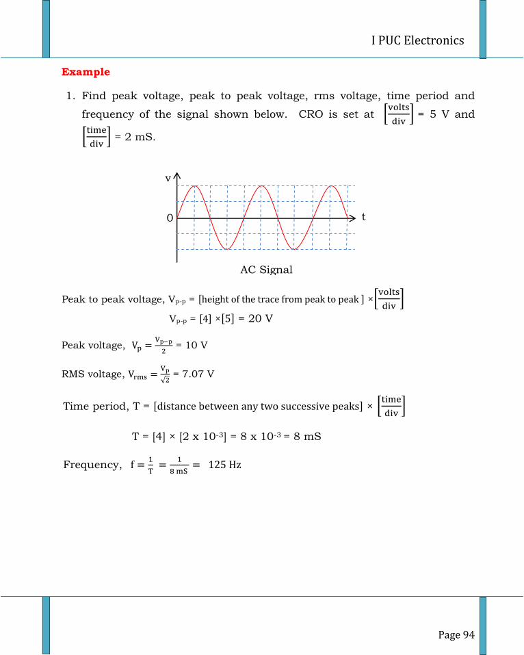
I PUC Electronics
Page 94
Example
1. Find peak voltage, peak to peak voltage, rms voltage, time period and
frequency of the signal shown below. CRO is set at [
] = 5 V and
[
] = 2 mS.
v
t
Peak to peak voltage, Vp-p = [ ] ×[
]
Vp-p = [ ] ×[ ] = 20 V
Peak voltage,
= 10 V
RMS voltage,
√ = 7.07 V
Time period, T = [ ] × [
]
T = [4] × [2 x 10-3] = 8 x 10-3 = 8 mS
Frequency,
0
AC Signal
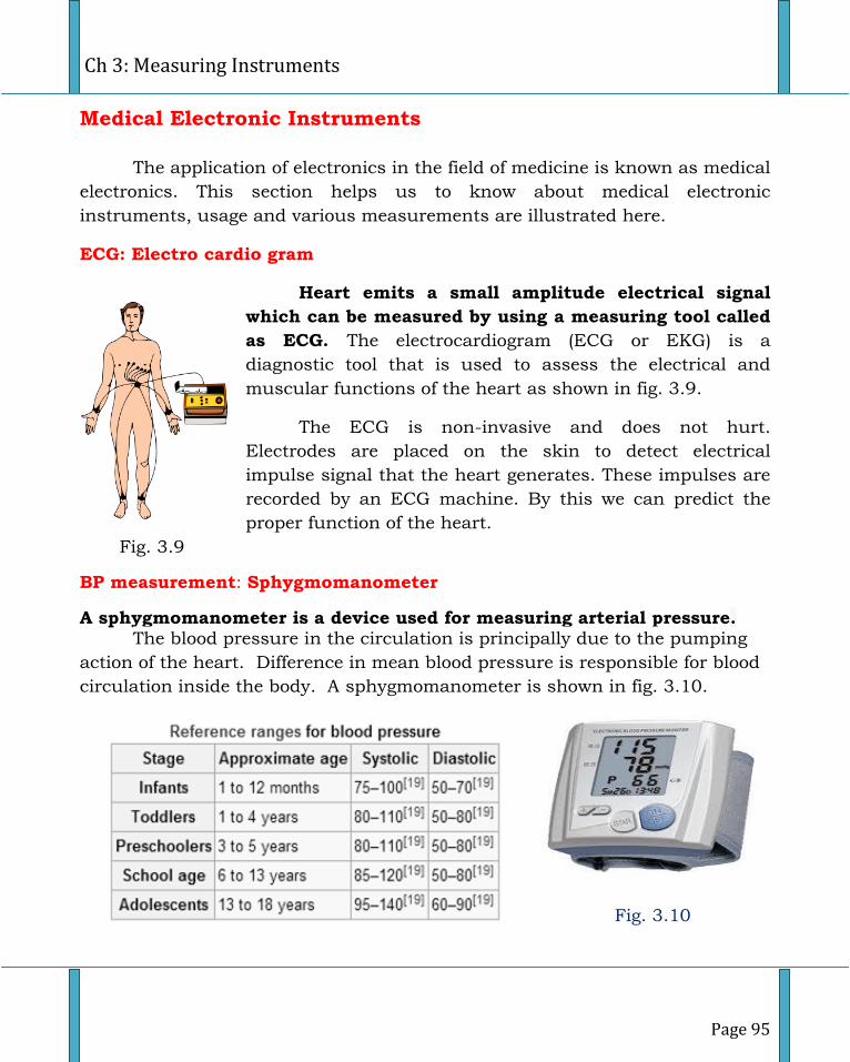
Ch 3: Measuring Instruments
Page 95
Medical Electronic Instruments
The application of electronics in the field of medicine is known as medical
electronics. This section helps us to know about medical electronic
instruments, usage and various measurements are illustrated here.
ECG: Electro cardio gram
Heart emits a small amplitude electrical signal
which can be measured by using a measuring tool called
as ECG. The electrocardiogram (ECG or EKG) is a
diagnostic tool that is used to assess the electrical and
muscular functions of the heart as shown in fig. 3.9.
The ECG is non-invasive and does not hurt.
Electrodes are placed on the skin to detect electrical
impulse signal that the heart generates. These impulses are
recorded by an ECG machine. By this we can predict the
proper function of the heart.
Fig. 3.9
BP measurement: Sphygmomanometer
A sphygmomanometer is a device used for measuring arterial pressure. The blood pressure in the circulation is principally due to the pumping
action of the heart. Difference in mean blood pressure is responsible for blood
circulation inside the body. A sphygmomanometer is shown in fig. 3.10.
Fig. 3.10

I PUC Electronics
Page 96
Systolic is the blood pressure when the blood is flowing through the arteries to
heart. Diastolic is the blood pressure when the blood is flowing through heart
to arteries. Systolic is greater than diastolic.
Glucometer
Glucometer is an electronic instrument that measures the concentration
of glucose present in the human blood. A small drop of blood, obtained by
pricking the skin with a lancet, is placed on a disposable test strip that the
meter reads and uses to calculate the blood glucose level. The meter then
displays the level in mg/dl (decilitre). The following table shows the values of
normal values of glucose level in the blood. Fig. 3.11 shows a glucometer.
Fig. 3.11 Glucometer
Ultra sound scan
An ultrasound scan is a test that uses sound waves to create images of
organs and structures inside the body. Since it uses sound waves and not
radiation, it is harmless.
Advantages and Applications:
Fig. 3.12 Picture showing the
Ultra sound scans Image.
Help to monitor the growth of an unborn
child, and check for the abnormalities.
Detect abnormalities of heart structures such
as the heart valves.
Detect abnormal widening of blood vessels.
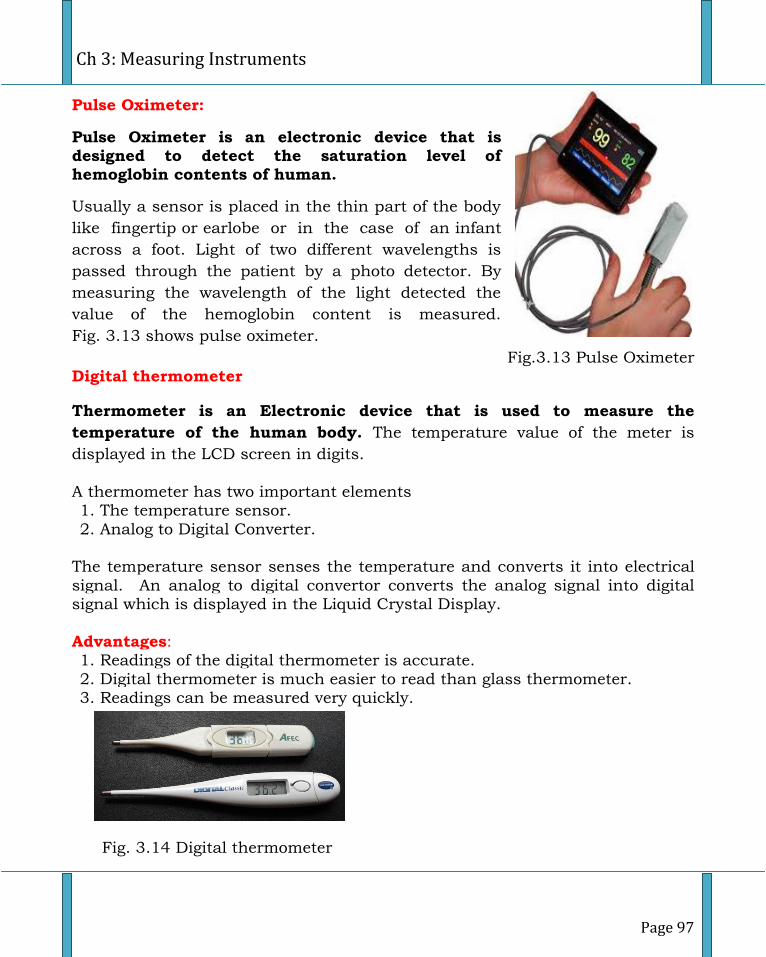
Ch 3: Measuring Instruments
Page 97
Pulse Oximeter:
Pulse Oximeter is an electronic device that is designed to detect the saturation level of hemoglobin contents of human.
Usually a sensor is placed in the thin part of the body
like fingertip or earlobe or in the case of an infant
across a foot. Light of two different wavelengths is
passed through the patient by a photo detector. By
measuring the wavelength of the light detected the
value of the hemoglobin content is measured.
Fig. 3.13 shows pulse oximeter.
Fig.3.13 Pulse Oximeter
Digital thermometer
Thermometer is an Electronic device that is used to measure the
temperature of the human body. The temperature value of the meter is
displayed in the LCD screen in digits.
A thermometer has two important elements 1. The temperature sensor.
2. Analog to Digital Converter.
The temperature sensor senses the temperature and converts it into electrical
signal. An analog to digital convertor converts the analog signal into digital signal which is displayed in the Liquid Crystal Display.
Advantages: 1. Readings of the digital thermometer is accurate.
2. Digital thermometer is much easier to read than glass thermometer. 3. Readings can be measured very quickly.
Fig. 3.14 Digital thermometer
I PUC Electronics
Page 98
Questions
One mark questions
1. What is meant by measurement?
2. What is an ammeter?
3. What is a voltmeter?
4. What is the Ohmmeter?
5. Write the symbol of Ohmmeter.
6. What is a multimeter?
7. What is an oscilloscope?
8. Expand ECG.
9. Mention any one application of an ECG.
10. What is BP measuring instrument?
11. What is glucometer?
12. What is an ultrasound scan?
13. Write an advantage of ultrasound scan?
14. What is a pulse oximeter?
15. What is a thermometer?
Two marks questions
16. Mention the merits of a multimeter.
17. Explain the controls of a multimeter.
18. Write any two application of an oscilloscope.
19. Mention any four controls of an oscilloscope.
20. What are the advantages of digital thermometer?
Ch-4: Passive Electronic Components
Page 99
Chapter 4
Passive electronic components
Introduction
The components used in electronic circuits are classified into two categories.
They are passive components and active components. This chapter is focussed
on passive components, their constructions, working and specifications.
Passive components
These components normally absorb, store or dissipate energy, but are unable
to supply energy to the network e.g. resistor, capacitor, inductor.
Active components
These components are able to supply energy to the circuit. They can also
rectify amplify and change energy from one form to another. Example: Vacuum
tube diode, semiconductor diode, Zener diode, varactor diode, LED, transistor,
FET, SCR, etc.
Resistor
Resistor is a component which is used to limit the flow of current. The
passive component which offers a specified value of resistance in the
circuit is known as a resistor. Resist means to oppose. All the materials offer
a little or more opposition to the flow of electric current through them. The
property of the material to oppose the flow of current is known as resistance.
The resistance of the material is not affected by the direction of flow of current
i.e. its effect is same for both AC and DC. The resistance of the material is
denoted by R and its SI unit is ohm (Ω).
Applications of resistor
Resistors are used to
1. Limit the current in a circuit.
2. Divide the voltage.
3. Protect the circuit elements.
4. Dissipate energy.
I PUC Electronics
Page 100
Specification of Resistors
Some important specification of resistors are ohms rating, power rating and
tolerance.
Ohms rating: It specifies the value of the maximum resistance offered by the
resistor when it is used in the circuit.
Power rating: The maximum power a resistor can dissipate safely is called
power rating. It is expressed in watts. Since P = I2R, therefore the power
dissipation of a resistor depends on the current flowing through it.
Tolerance value: The percentage variation in the resistance value with respect
to its marked value is called tolerance. Resistors have tolerance value of about
±1 % to ±20 %.
Temperature coefficient: The resistance of the material also depends on its
temperature. Hence temperature coefficient specifies how resistance varies with
temperature. In all the conducting materials, resistance increases with
increases in temperature but in semiconductor materials, the resistance
decreases with an increase in temperature. Temperature coefficient of
resistance expressed as,
From the above equation,
The temperature coefficient of resistance ( ) may be defined as the increase in
resistance per ºC rise in temperature to its resistance at 0ºC.
Where Rt = Resistance at tº C in Ω.
Ro = Resistance at 0ºC in Ω.
Illustration1
The resistance of a coil made of copper wire is 100 Ω at 0 ºC. Calculate its
resistance at 30 ºC. Given = 0.004/ ºC.
Ch-4: Passive Electronic Components
Page 101
Solution: Given, Resistance at 0 ºC, Ro = 100 Ω
Temperature t = 30 ºC
Temperature Coefficient, = 0.004 / ºC Hence, resistance at t ºC,
Rt = Ro (1 + t)
= 100 (1 + 0.004 x 30)
= 100 x 1.12
= 112 Ω
Specific resistance or resistivity
At constant temperature, resistance of a conductor is directly
proportional to the length of the conductor l and inversely proportional to the
area of cross section A.
R =
Where, ρ is a constant depending on the nature of the material of the
conductor and is known as specific resistance or resistivity of that material.
Consider the equation, R =
, if l = 1 m and A = 1 m2, then R = ρ.
Thus, Specific resistance or resistivity of the conducting material is defined as
the resistance of a conductor of unit length having unit cross sectional area.
The SI unit of specific resistance is Ohm meter (Ωm).
Illustration:
1) The resistance of a wire of length 1 m and of diameter 0.12 mm is 40 Ω.
What is its specific resistance?
I PUC Electronics
Page 102
Solution: Given, l = 1 m, d = 0.12 mm, R = 40 Ω, ρ =?
Then, Specific resistance =
=
=
( )
= 0.45216 X 10⁻⁶ Ωm
Conductance (G)
Conductance is the property of the material which allows the current to flow
through it or in other words conductance is the reciprocal of resistance. It is
measured in Siemens.
G =
Types of Resistors
Resistors are broadly classified into two types, they are
1. Fixed resistor
2. Variable resistor
A fixed resistor is one whose resistance value remains constant; however
there may be some variation in their value due to temperature variation. They
are further classified depending upon the type of material used for
construction. They are
1. Carbon composition resistor
2. Metal film resistor
3. Surface mount device (SMD) resistor
4. Wire wound resistor, etc.
A variable resistor is one whose resistance value can be varied over a
specified range. They are further classified based on the materials used and
type of construction. They are
1. Potentiometer
2. Preset
3. Rheostat, etc.
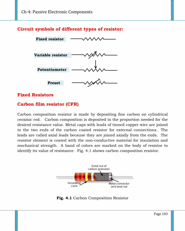
Ch-4: Passive Electronic Components
Page 103
Circuit symbols of different types of resistor:
Fixed Resistors
Carbon film resistor (CFR)
Carbon composition resistor is made by depositing fine carbon on cylindrical
ceramic rod. Carbon composition is deposited in the proportion needed for the
desired resistance value. Metal caps with leads of tinned copper wire are joined
to the two ends of the carbon coated resistor for external connections. The
leads are called axial leads because they are joined axially from the ends. The
resistor element is coated with the non-conductive material for insulation and
mechanical strength. A band of colors are marked on the body of resistor to
identify its value of resistance. Fig. 4.1 shows carbon composition resistor.
Fig. 4.1 Carbon Composition Resistor
Fixed resistor
Variable resistor
Potentiometer
Preset
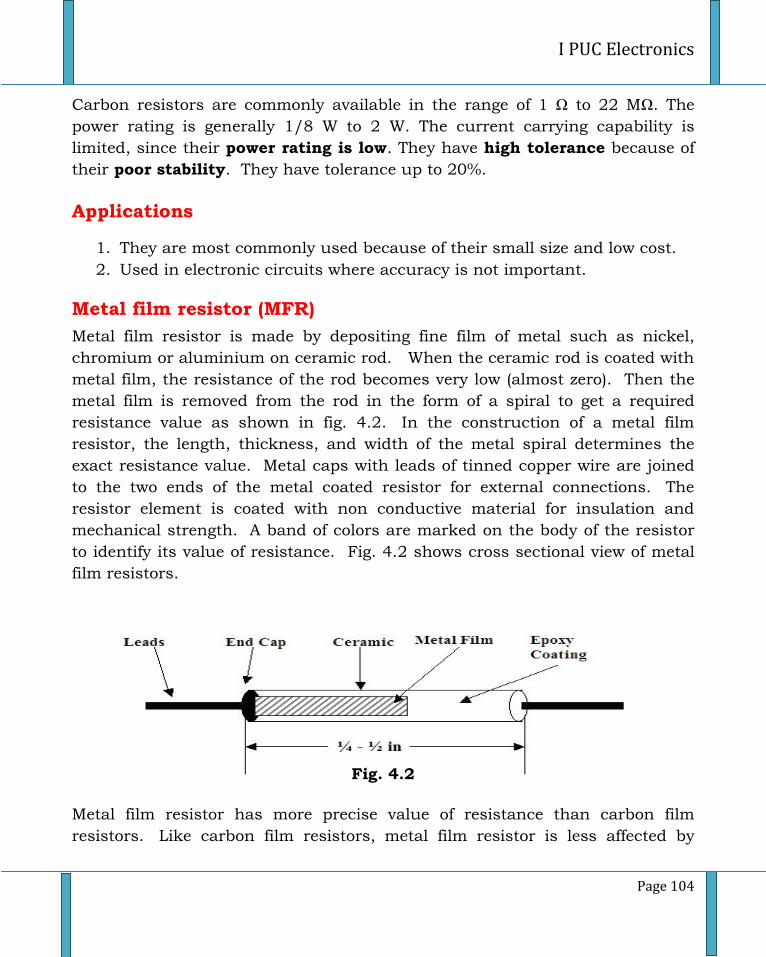
I PUC Electronics
Page 104
Carbon resistors are commonly available in the range of 1 Ω to 22 MΩ. The
power rating is generally 1/8 W to 2 W. The current carrying capability is
limited, since their power rating is low. They have high tolerance because of
their poor stability. They have tolerance up to 20%.
Applications
1. They are most commonly used because of their small size and low cost.
2. Used in electronic circuits where accuracy is not important.
Metal film resistor (MFR)
Metal film resistor is made by depositing fine film of metal such as nickel,
chromium or aluminium on ceramic rod. When the ceramic rod is coated with
metal film, the resistance of the rod becomes very low (almost zero). Then the
metal film is removed from the rod in the form of a spiral to get a required
resistance value as shown in fig. 4.2. In the construction of a metal film
resistor, the length, thickness, and width of the metal spiral determines the
exact resistance value. Metal caps with leads of tinned copper wire are joined
to the two ends of the metal coated resistor for external connections. The
resistor element is coated with non conductive material for insulation and
mechanical strength. A band of colors are marked on the body of the resistor
to identify its value of resistance. Fig. 4.2 shows cross sectional view of metal
film resistors.
Fig. 4.2
Metal film resistor has more precise value of resistance than carbon film
resistors. Like carbon film resistors, metal film resistor is less affected by
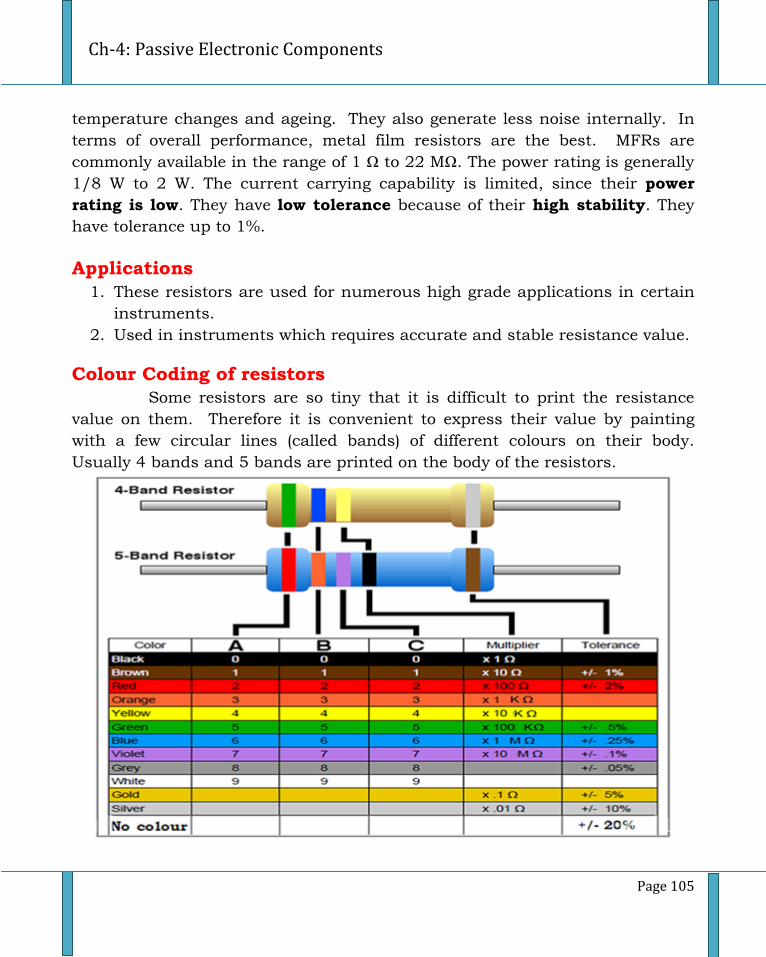
Ch-4: Passive Electronic Components
Page 105
temperature changes and ageing. They also generate less noise internally. In
terms of overall performance, metal film resistors are the best. MFRs are
commonly available in the range of 1 Ω to 22 MΩ. The power rating is generally
1/8 W to 2 W. The current carrying capability is limited, since their power
rating is low. They have low tolerance because of their high stability. They
have tolerance up to 1%.
Applications
1. These resistors are used for numerous high grade applications in certain
instruments.
2. Used in instruments which requires accurate and stable resistance value.
Colour Coding of resistors
Some resistors are so tiny that it is difficult to print the resistance
value on them. Therefore it is convenient to express their value by painting
with a few circular lines (called bands) of different colours on their body.
Usually 4 bands and 5 bands are printed on the body of the resistors.
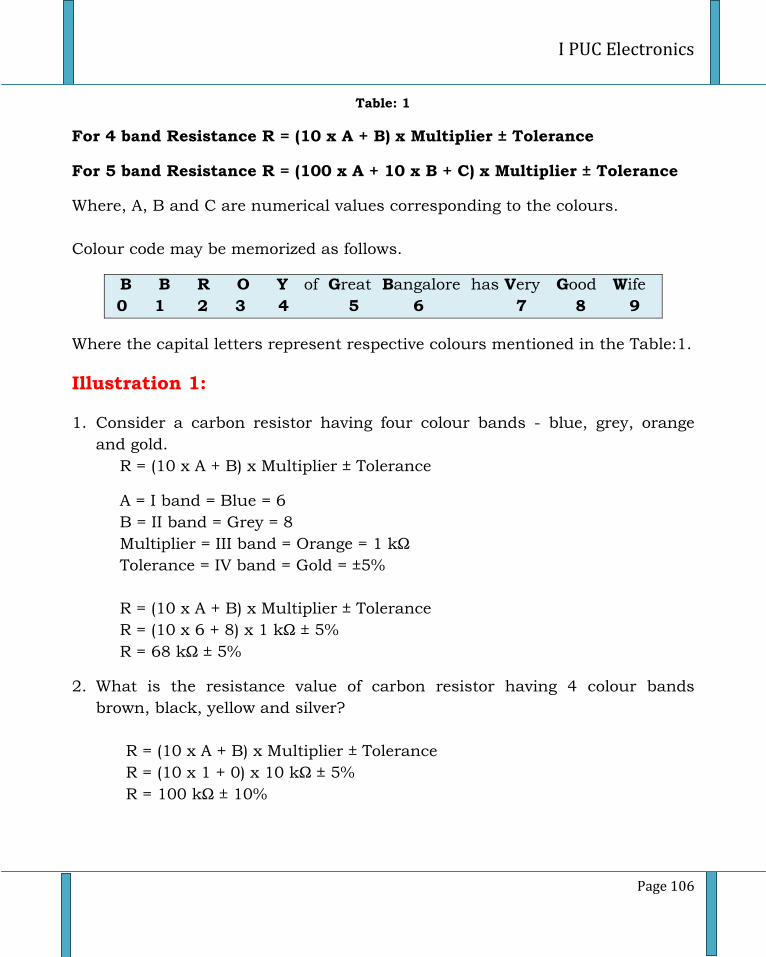
I PUC Electronics
Page 106
Table: 1
For 4 band Resistance R = (10 x A + B) x Multiplier ± Tolerance
For 5 band Resistance R = (100 x A + 10 x B + C) x Multiplier ± Tolerance
Where, A, B and C are numerical values corresponding to the colours.
Colour code may be memorized as follows.
B B R O Y of Great Bangalore has Very Good Wife
0 1 2 3 4 5 6 7 8 9
Where the capital letters represent respective colours mentioned in the Table:1.
Illustration 1:
1. Consider a carbon resistor having four colour bands - blue, grey, orange
and gold.
R = (10 x A + B) x Multiplier ± Tolerance
A = I band = Blue = 6
B = II band = Grey = 8
Multiplier = III band = Orange = 1 kΩ
Tolerance = IV band = Gold = ±5%
R = (10 x A + B) x Multiplier ± Tolerance
R = (10 x 6 + 8) x 1 kΩ ± 5%
R = 68 kΩ ± 5%
2. What is the resistance value of carbon resistor having 4 colour bands
brown, black, yellow and silver?
R = (10 x A + B) x Multiplier ± Tolerance
R = (10 x 1 + 0) x 10 kΩ ± 5%
R = 100 kΩ ± 10%
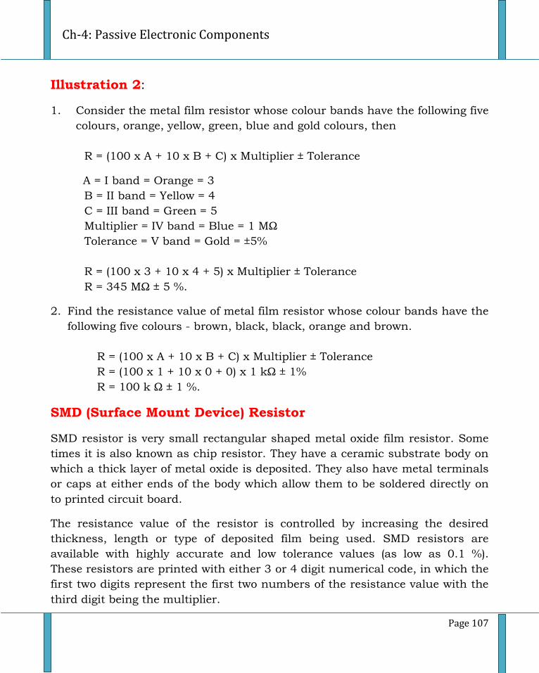
Ch-4: Passive Electronic Components
Page 107
Illustration 2:
1. Consider the metal film resistor whose colour bands have the following five
colours, orange, yellow, green, blue and gold colours, then
R = (100 x A + 10 x B + C) x Multiplier ± Tolerance
A = I band = Orange = 3
B = II band = Yellow = 4
C = III band = Green = 5
Multiplier = IV band = Blue = 1 MΩ
Tolerance = V band = Gold = ±5%
R = (100 x 3 + 10 x 4 + 5) x Multiplier ± Tolerance
R = 345 MΩ ± 5 %.
2. Find the resistance value of metal film resistor whose colour bands have the
following five colours - brown, black, black, orange and brown.
R = (100 x A + 10 x B + C) x Multiplier ± Tolerance
R = (100 x 1 + 10 x 0 + 0) x 1 kΩ ± 1%
R = 100 k Ω ± 1 %.
SMD (Surface Mount Device) Resistor
SMD resistor is very small rectangular shaped metal oxide film resistor. Some
times it is also known as chip resistor. They have a ceramic substrate body on
which a thick layer of metal oxide is deposited. They also have metal terminals
or caps at either ends of the body which allow them to be soldered directly on
to printed circuit board.
The resistance value of the resistor is controlled by increasing the desired
thickness, length or type of deposited film being used. SMD resistors are
available with highly accurate and low tolerance values (as low as 0.1 %).
These resistors are printed with either 3 or 4 digit numerical code, in which the
first two digits represent the first two numbers of the resistance value with the
third digit being the multiplier.
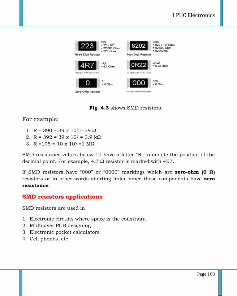
I PUC Electronics
Page 108
Fig. 4.3 shows SMD resistors.
For example:
1. R = 390 = 39 x 100 = 39 Ω
2. R = 392 = 39 x 102 = 3.9 kΩ
3. R =105 = 10 x 105 =1 MΩ
SMD resistance values below 10 have a letter “R” to denote the position of the
decimal point. For example, 4.7 Ω resistor is marked with 4R7.
If SMD resistors have “000” or “0000” markings which are zero-ohm (0 Ω)
resistors or in other words shorting links, since these components have zero
resistance.
SMD resistors applications
SMD resistors are used in
1. Electronic circuits where space is the constraint
2. Multilayer PCB designing
3. Electronic pocket calculators
4. Cell phones, etc.
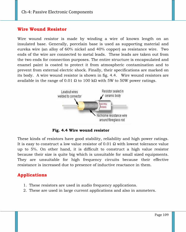
Ch-4: Passive Electronic Components
Page 109
Wire Wound Resistor
Wire wound resistor is made by winding a wire of known length on an
insulated base. Generally, porcelain base is used as supporting material and
eureka wire (an alloy of 60% nickel and 40% copper) as resistance wire. Two
ends of the wire are connected to metal leads. These leads are taken out from
the two ends for connection purposes. The entire structure is encapsulated and
enamel paint is coated to protect it from atmospheric contamination and to
prevent from external electric shock. Finally, their specifications are marked on
its body. A wire wound resistor is shown in fig. 4.4. Wire wound resistors are
available in the range of 0.01 Ω to 100 kΩ with 5W to 50W power ratings.
Fig. 4.4 Wire wound resistor
These kinds of resistors have good stability, reliability and high power ratings.
It is easy to construct a low value resistor of 0.01 Ω with lowest tolerance value
up to 5%. On other hand, it is difficult to construct a high value resistor
because their size is quite big which is unsuitable for small sized equipments.
They are unsuitable for high frequency circuits because their effective
resistance is increased due to presence of inductive reactance in them.
Applications
1. These resistors are used in audio frequency applications.
2. These are used in large current applications and also in ammeters.
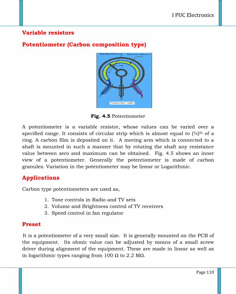
I PUC Electronics
Page 110
Variable resistors
Potentiometer (Carbon composition type)
Fig. 4.5 Potentiometer
A potentiometer is a variable resistor, whose values can be varied over a
specified range. It consists of circular strip which is almost equal to (¾)th of a
ring. A carbon film is deposited on it. A moving arm which is connected to a
shaft is mounted in such a manner that by rotating the shaft any resistance
value between zero and maximum can be obtained. Fig. 4.5 shows an inner
view of a potentiometer. Generally the potentiometer is made of carbon
granules. Variation in the potentiometer may be linear or Logarithmic.
Applications
Carbon type potentiometers are used as,
1. Tone controls in Radio and TV sets
2. Volume and Brightness control of TV receivers
3. Speed control in fan regulator
Preset
It is a potentiometer of a very small size. It is generally mounted on the PCB of
the equipment. Its ohmic value can be adjusted by means of a small screw
driver during alignment of the equipment. These are made in linear as well as
in logarithmic types ranging from 100 Ω to 2.2 MΩ.
Ch-4: Passive Electronic Components
Page 111
Applications
1. They are extensively used in TV receivers.
2. They are used in electronic circuits for calibration purposes.
Importance of resistor power rating
When the current flows through a resistor, power is dissipated by the resistor
in the form of heat. The maximum power a resistor can withstand without
damaging it is known as the power rating of a resistor. Every resistor has a
maximum power rating which is determined by its physical size. Generally, the
greater the size, the more power it can dissipate safely without degrading its
performance.
The electrical power dissipation of any resistor in a DC circuit can be
calculated using one of the following three formulae.
Power (P) = V I = I2 R =
Where V is the voltage across the resistor, I is the current flowing through the
resistor and R is the resistance of the resistor in Ohm (Ω).
Resistors of the same ohmic value are available in different power or wattage
ratings. CFR and MFR resistors are commonly available in wattage ratings of
(⅛) W, (¼) W, (½) W, 1 W, and 2 W. However, it is always better to select a
particular wattage resistor that is capable of dissipating two or more times the
calculated power. When resistors with higher wattage ratings are required, wire
wound resistors are generally used to dissipate the excessive heat.
Note: The common problems in resistors are open, short and ageing of resistor.
1. Open circuited resistor: When large current flows through the
resistor, it burns out and opens. An open circuited resistor has infinite
resistance and no current flows through the resistor.
2. Short circuited resistor: A short circuit has zero resistance. But
practically it is impossible for a resistor to become short.
3. Ageing of resistor: The deterioration in the value of resistor due to
long period use is called ageing of resistor. The tolerance value of the aged
resistor varies.
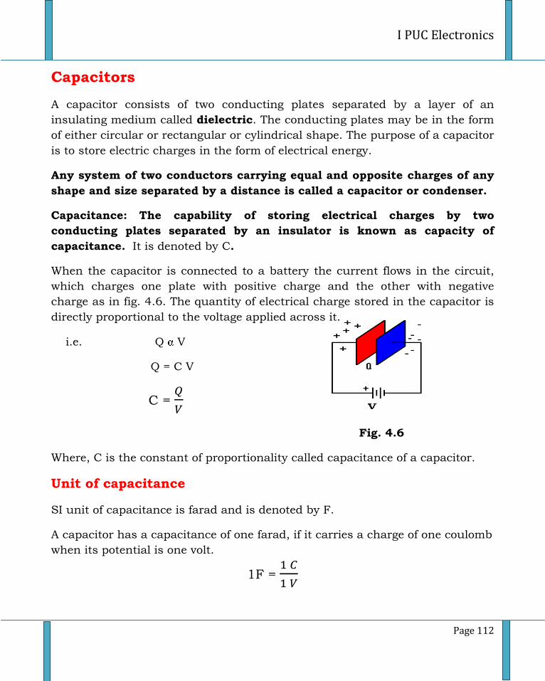
I PUC Electronics
Page 112
Capacitors
A capacitor consists of two conducting plates separated by a layer of an
insulating medium called dielectric. The conducting plates may be in the form
of either circular or rectangular or cylindrical shape. The purpose of a capacitor
is to store electric charges in the form of electrical energy.
Any system of two conductors carrying equal and opposite charges of any
shape and size separated by a distance is called a capacitor or condenser.
Capacitance: The capability of storing electrical charges by two
conducting plates separated by an insulator is known as capacity of
capacitance. It is denoted by C.
When the capacitor is connected to a battery the current flows in the circuit,
which charges one plate with positive charge and the other with negative
charge as in fig. 4.6. The quantity of electrical charge stored in the capacitor is
directly proportional to the voltage applied across it.
i.e. Q V
Q = C V
C =
Fig. 4.6
Where, C is the constant of proportionality called capacitance of a capacitor.
Unit of capacitance
SI unit of capacitance is farad and is denoted by F.
A capacitor has a capacitance of one farad, if it carries a charge of one coulomb
when its potential is one volt.
1F =
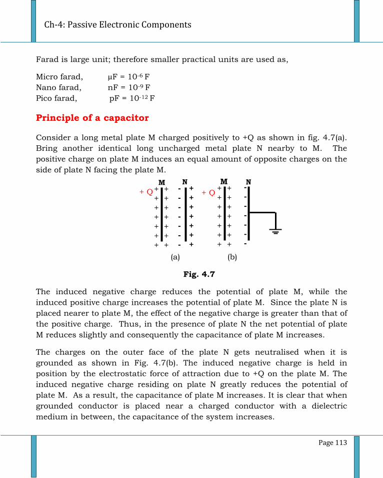
Ch-4: Passive Electronic Components
Page 113
Farad is large unit; therefore smaller practical units are used as,
Micro farad, µF = 10-6 F
Nano farad, nF = 10-9 F
Pico farad, pF = 10-12 F
Principle of a capacitor
Consider a long metal plate M charged positively to +Q as shown in fig. 4.7(a).
Bring another identical long uncharged metal plate N nearby to M. The
positive charge on plate M induces an equal amount of opposite charges on the
side of plate N facing the plate M.
(a) (b)
Fig. 4.7
The induced negative charge reduces the potential of plate M, while the
induced positive charge increases the potential of plate M. Since the plate N is
placed nearer to plate M, the effect of the negative charge is greater than that of
the positive charge. Thus, in the presence of plate N the net potential of plate
M reduces slightly and consequently the capacitance of plate M increases.
The charges on the outer face of the plate N gets neutralised when it is
grounded as shown in Fig. 4.7(b). The induced negative charge is held in
position by the electrostatic force of attraction due to +Q on the plate M. The
induced negative charge residing on plate N greatly reduces the potential of
plate M. As a result, the capacitance of plate M increases. It is clear that when
grounded conductor is placed near a charged conductor with a dielectric
medium in between, the capacitance of the system increases.
+ Q
M N N M + + + +
+ + + +
+ + + + + +
-
- - -
- - -
- +
- + - +
- + - + - +
- +
+ + + +
+ + + +
+ + + + + +
+ Q
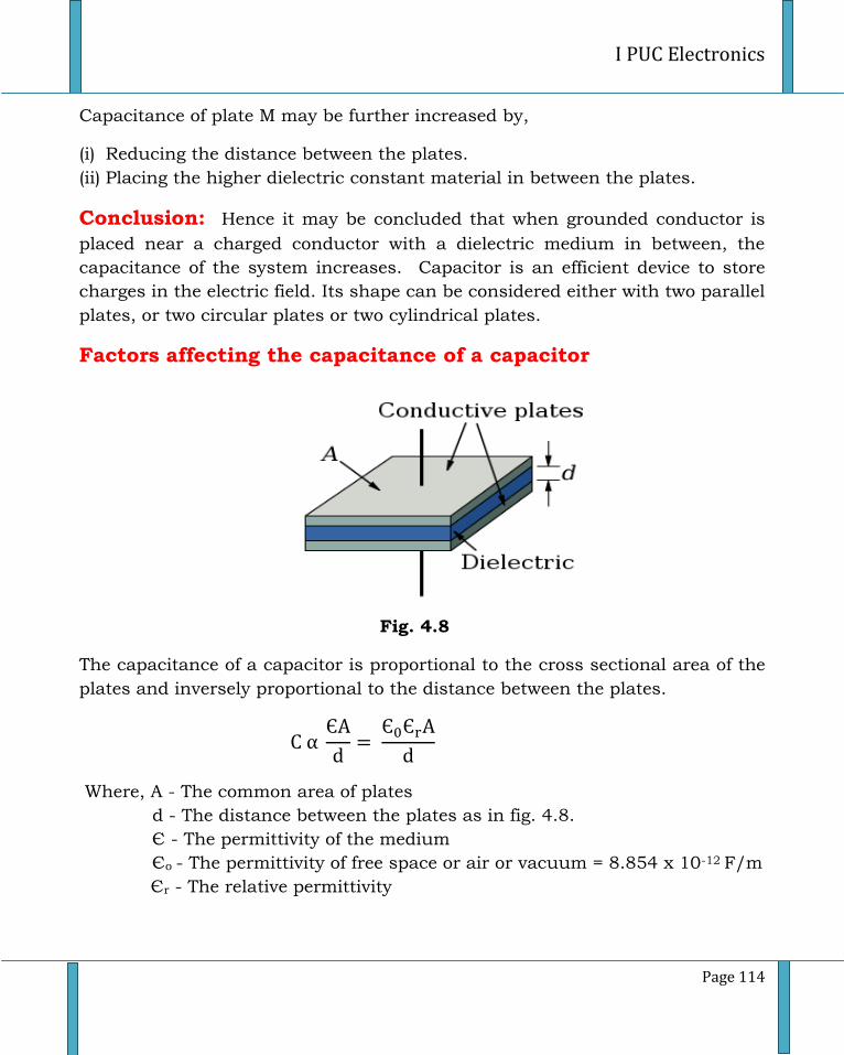
I PUC Electronics
Page 114
Capacitance of plate M may be further increased by,
(i) Reducing the distance between the plates.
(ii) Placing the higher dielectric constant material in between the plates.
Conclusion: Hence it may be concluded that when grounded conductor is
placed near a charged conductor with a dielectric medium in between, the
capacitance of the system increases. Capacitor is an efficient device to store
charges in the electric field. Its shape can be considered either with two parallel
plates, or two circular plates or two cylindrical plates.
Factors affecting the capacitance of a capacitor
Fig. 4.8
The capacitance of a capacitor is proportional to the cross sectional area of the
plates and inversely proportional to the distance between the plates.
Where, A - The common area of plates
d - The distance between the plates as in fig. 4.8.
Є - The permittivity of the medium
Єo - The permittivity of free space or air or vacuum = 8.854 x 10⁻¹² F/m
Єr - The relative permittivity
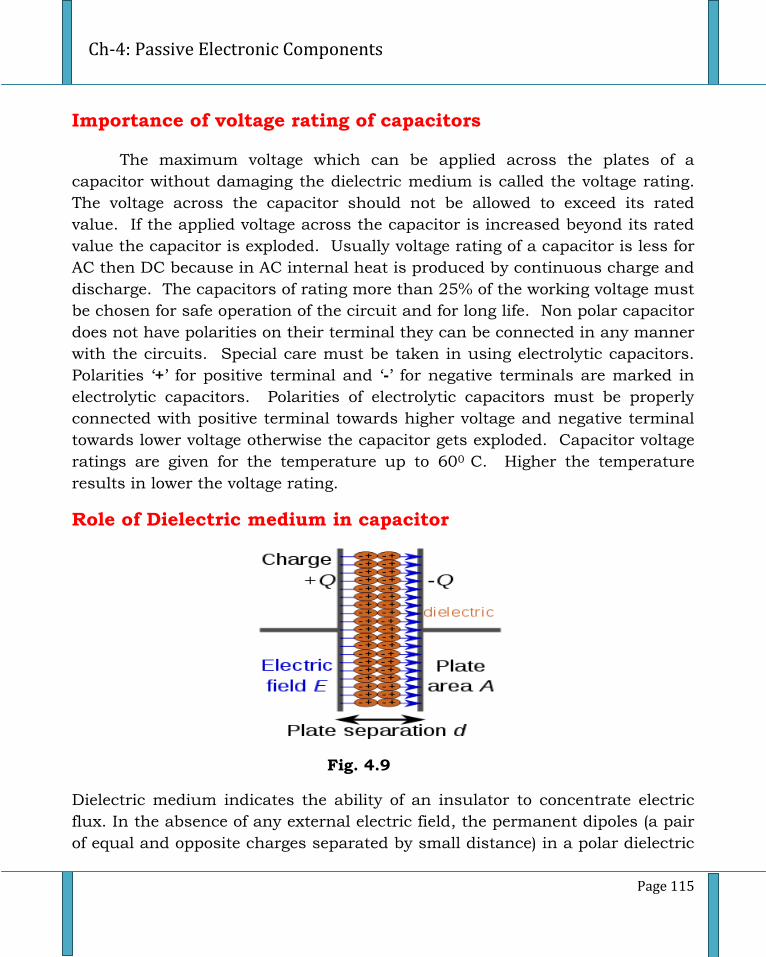
Ch-4: Passive Electronic Components
Page 115
Importance of voltage rating of capacitors
The maximum voltage which can be applied across the plates of a
capacitor without damaging the dielectric medium is called the voltage rating.
The voltage across the capacitor should not be allowed to exceed its rated
value. If the applied voltage across the capacitor is increased beyond its rated
value the capacitor is exploded. Usually voltage rating of a capacitor is less for
AC then DC because in AC internal heat is produced by continuous charge and
discharge. The capacitors of rating more than 25% of the working voltage must
be chosen for safe operation of the circuit and for long life. Non polar capacitor
does not have polarities on their terminal they can be connected in any manner
with the circuits. Special care must be taken in using electrolytic capacitors.
Polarities ‘+’ for positive terminal and ‘-’ for negative terminals are marked in
electrolytic capacitors. Polarities of electrolytic capacitors must be properly
connected with positive terminal towards higher voltage and negative terminal
towards lower voltage otherwise the capacitor gets exploded. Capacitor voltage
ratings are given for the temperature up to 600 C. Higher the temperature
results in lower the voltage rating.
Role of Dielectric medium in capacitor
Fig. 4.9
Dielectric medium indicates the ability of an insulator to concentrate electric
flux. In the absence of any external electric field, the permanent dipoles (a pair
of equal and opposite charges separated by small distance) in a polar dielectric
I PUC Electronics
Page 116
will be oriented in a random manner. Under the action of electric field positive
and negative charges in an atom get displaced in opposite direction. This effect
induces an electric dipole in the dielectric medium along the direction of the
applied field. Hence dielectric medium is said to be polarized. Due to this
process electric field is established inside the medium. The developed internal
field opposes the external electric field. Usually the net field inside a dielectric
is less than the applied field. This decreases potential difference between the
plates and consequently more charges are stored in the capacitor. A typically
polarized structure inside the dielectric medium is shown in fig. 4.9.
The Table given below shows some of the dielectric materials and their
constants.
Name of insulator Dielectric
constant (Єr)
Paper
Bakelite
Porcelain
Mica
Air
Polystyrene
Glass
Ceramic (Barium strontium oxide)
Ceramic (Strontium titanate)
Titanium Ceramic
3.7
4.9
6.0
5.0
1.006
2.6
7.5
7500
310
130
Energy stored in a capacitor
A capacitor C can be charged by connecting a battery of V volt. Capacitor gets
charged with Q coulomb of charge. The energy stored in the charged capacitor
is measured by the amount of work done in charging the capacitor to a given
potential. If V is the voltage across a capacitor of capacitance C, then the
electric energy stored in the capacitor is given by
C joule
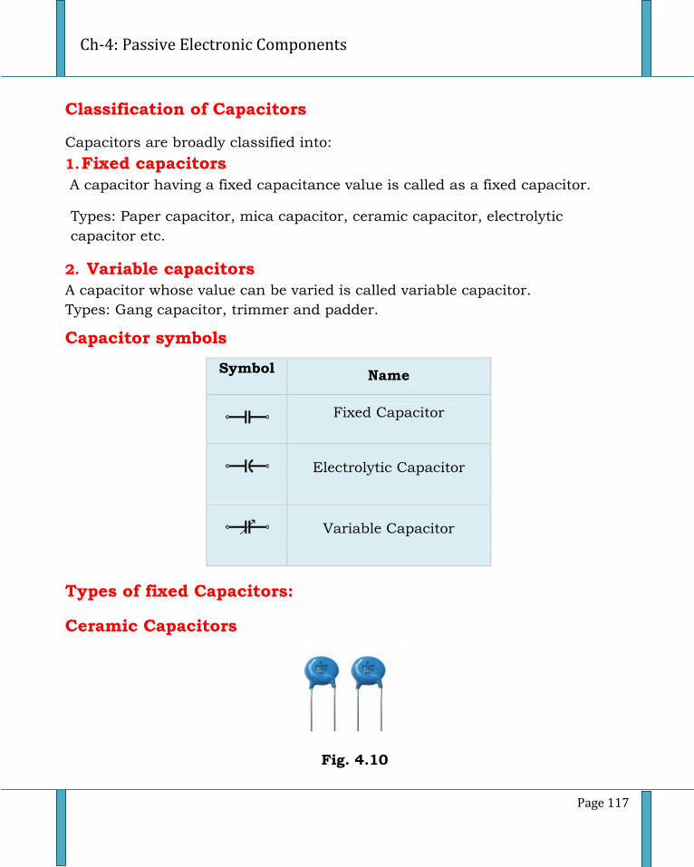
Ch-4: Passive Electronic Components
Page 117
Classification of Capacitors
Capacitors are broadly classified into:
1. Fixed capacitors
A capacitor having a fixed capacitance value is called as a fixed capacitor.
Types: Paper capacitor, mica capacitor, ceramic capacitor, electrolytic
capacitor etc.
2. Variable capacitors
A capacitor whose value can be varied is called variable capacitor.
Types: Gang capacitor, trimmer and padder.
Capacitor symbols
Symbol Name
Fixed Capacitor
Electrolytic Capacitor
Variable Capacitor
Types of fixed Capacitors:
Ceramic Capacitors
Fig. 4.10
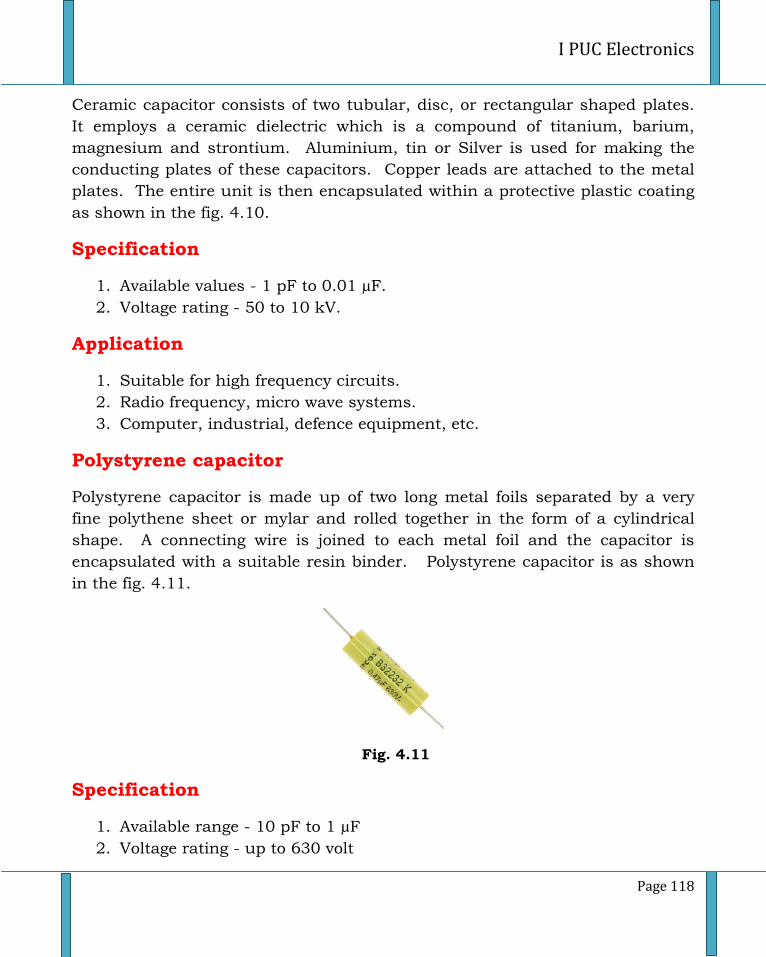
I PUC Electronics
Page 118
Ceramic capacitor consists of two tubular, disc, or rectangular shaped plates.
It employs a ceramic dielectric which is a compound of titanium, barium,
magnesium and strontium. Aluminium, tin or Silver is used for making the
conducting plates of these capacitors. Copper leads are attached to the metal
plates. The entire unit is then encapsulated within a protective plastic coating
as shown in the fig. 4.10.
Specification
1. Available values - 1 pF to 0.01 µF.
2. Voltage rating - 50 to 10 kV.
Application
1. Suitable for high frequency circuits.
2. Radio frequency, micro wave systems.
3. Computer, industrial, defence equipment, etc.
Polystyrene capacitor
Polystyrene capacitor is made up of two long metal foils separated by a very
fine polythene sheet or mylar and rolled together in the form of a cylindrical
shape. A connecting wire is joined to each metal foil and the capacitor is
encapsulated with a suitable resin binder. Polystyrene capacitor is as shown
in the fig. 4.11.
Fig. 4.11
Specification
1. Available range - 10 pF to 1 µF
2. Voltage rating - up to 630 volt
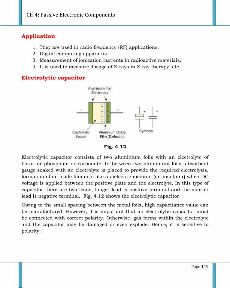
Ch-4: Passive Electronic Components
Page 119
Application
1. They are used in radio frequency (RF) applications.
2. Digital computing apparatus.
3. Measurement of ionization currents in radioactive materials.
4. It is used to measure dosage of X-rays in X-ray therapy, etc.
Electrolytic capacitor
Fig. 4.12
Electrolytic capacitor consists of two aluminium foils with an electrolyte of
borax or phosphate or carbonate. In between two aluminium foils, absorbent
gauge soaked with an electrolyte is placed to provide the required electrolysis,
formation of an oxide film acts like a dielectric medium (an insulator) when DC
voltage is applied between the positive plate and the electrolyte. In this type of
capacitor there are two leads, longer lead is positive terminal and the shorter
lead is negative terminal. Fig. 4.12 shows the electrolytic capacitor.
Owing to the small spacing between the metal foils, high capacitance value can
be manufactured. However, it is important that an electrolytic capacitor must
be connected with correct polarity. Otherwise, gas forms within the electrolyte
and the capacitor may be damaged or even explode. Hence, it is sensitive to
polarity.
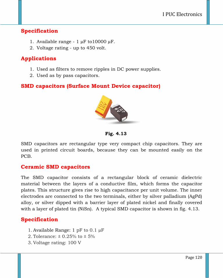
I PUC Electronics
Page 120
Specification
1. Available range - 1 µF to10000 µF.
2. Voltage rating - up to 450 volt.
Applications
1. Used as filters to remove ripples in DC power supplies.
2. Used as by pass capacitors.
SMD capacitors (Surface Mount Device capacitor)
Fig. 4.13
SMD capacitors are rectangular type very compact chip capacitors. They are
used in printed circuit boards, because they can be mounted easily on the
PCB.
Ceramic SMD capacitors
The SMD capacitor consists of a rectangular block of ceramic dielectric
material between the layers of a conductive film, which forms the capacitor
plates. This structure gives rise to high capacitance per unit volume. The inner
electrodes are connected to the two terminals, either by silver palladium (AgPd)
alloy, or silver dipped with a barrier layer of plated nickel and finally covered
with a layer of plated tin (NiSn). A typical SMD capacitor is shown in fig. 4.13.
Specification
1. Available Range: 1 pF to 0.1 µF
2. Tolerance: ± 0.25% to ± 5%
3. Voltage rating: 100 V
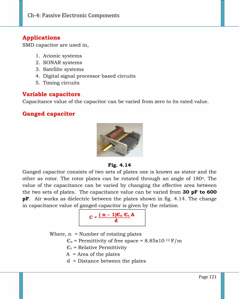
Ch-4: Passive Electronic Components
Page 121
Applications
SMD capacitor are used in,
1. Avionic systems
2. SONAR systems
3. Satellite systems
4. Digital signal processor based circuits
5. Timing circuits
Variable capacitors
Capacitance value of the capacitor can be varied from zero to its rated value.
Ganged capacitor
Fig. 4.14
Ganged capacitor consists of two sets of plates one is known as stator and the
other as rotor. The rotor plates can be rotated through an angle of 180o. The
value of the capacitance can be varied by changing the effective area between
the two sets of plates. The capacitance value can be varied from 30 pF to 600
pF. Air works as dielectric between the plates shown in fig. 4.14. The change
in capacitance value of ganged capacitor is given by the relation
Where, n = Number of rotating plates
Єo = Permittivity of free space = 8.85x10⁻¹² F/m
Єr = Relative Permittivity
A = Area of the plates
d = Distance between the plates
C = ( n 1)Єo Єr A
d
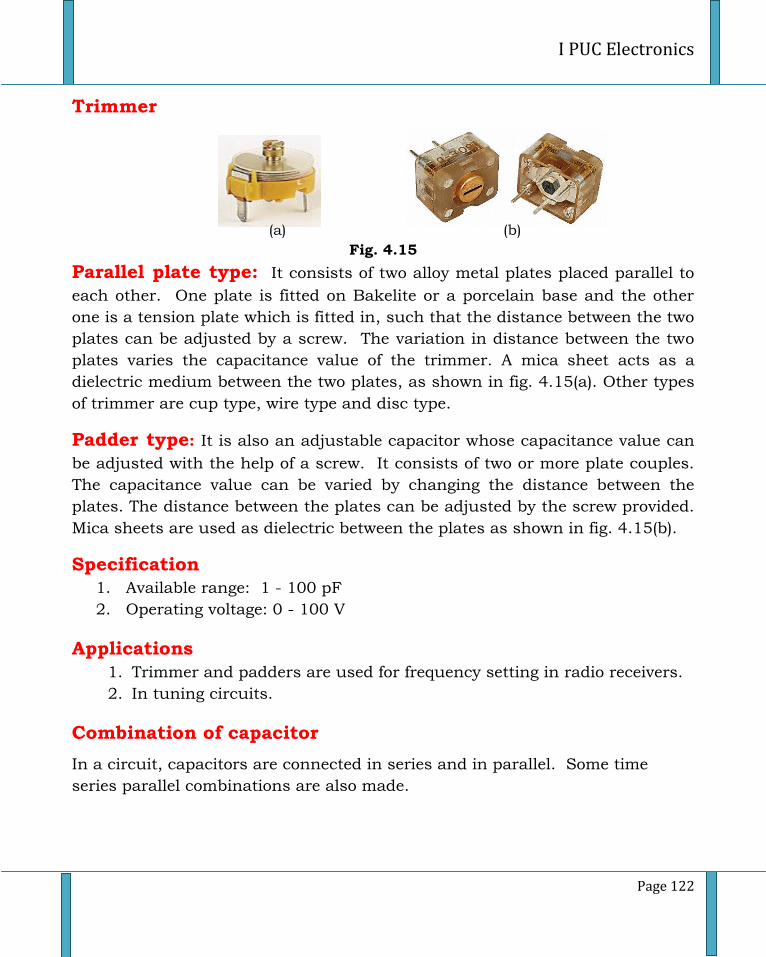
I PUC Electronics
Page 122
Trimmer
(a) (b)
Fig. 4.15
Parallel plate type: It consists of two alloy metal plates placed parallel to
each other. One plate is fitted on Bakelite or a porcelain base and the other
one is a tension plate which is fitted in, such that the distance between the two
plates can be adjusted by a screw. The variation in distance between the two
plates varies the capacitance value of the trimmer. A mica sheet acts as a
dielectric medium between the two plates, as shown in fig. 4.15(a). Other types
of trimmer are cup type, wire type and disc type.
Padder type: It is also an adjustable capacitor whose capacitance value can
be adjusted with the help of a screw. It consists of two or more plate couples.
The capacitance value can be varied by changing the distance between the
plates. The distance between the plates can be adjusted by the screw provided.
Mica sheets are used as dielectric between the plates as shown in fig. 4.15(b).
Specification
1. Available range: 1 - 100 pF
2. Operating voltage: 0 - 100 V
Applications
1. Trimmer and padders are used for frequency setting in radio receivers.
2. In tuning circuits.
Combination of capacitor
In a circuit, capacitors are connected in series and in parallel. Some time
series parallel combinations are also made.
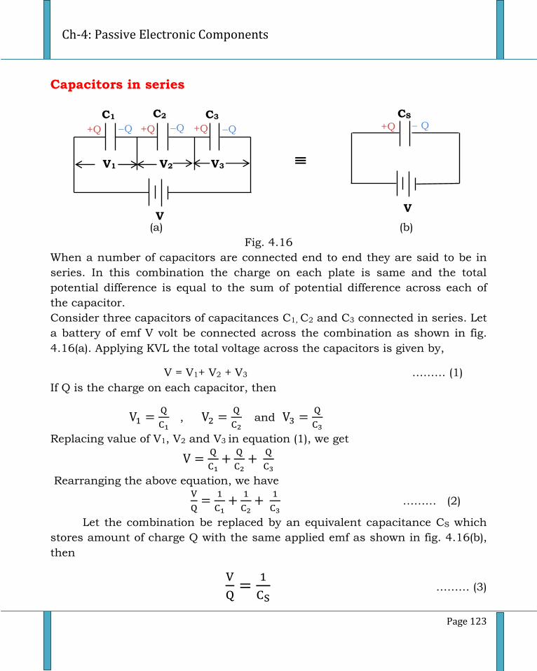
Ch-4: Passive Electronic Components
Page 123
Capacitors in series
(a) (b)
Fig. 4.16
When a number of capacitors are connected end to end they are said to be in
series. In this combination the charge on each plate is same and the total
potential difference is equal to the sum of potential difference across each of
the capacitor.
Consider three capacitors of capacitances C1, C2 and C3 connected in series. Let
a battery of emf V volt be connected across the combination as shown in fig.
4.16(a). Applying KVL the total voltage across the capacitors is given by,
V = V1+ V2 + V3 ……… (1)
If Q is the charge on each capacitor, then
,
and
Replacing value of V1, V2 and V3 in equation (1), we get
Rearranging the above equation, we have
……… (2)
Let the combination be replaced by an equivalent capacitance CS which
stores amount of charge Q with the same applied emf as shown in fig. 4.16(b),
then
……… (3)
≡
Q
+Q
CS
V
+Q
V1 V2
Q
V
C1 C2 C3
V3
+Q
+Q
Q
Q
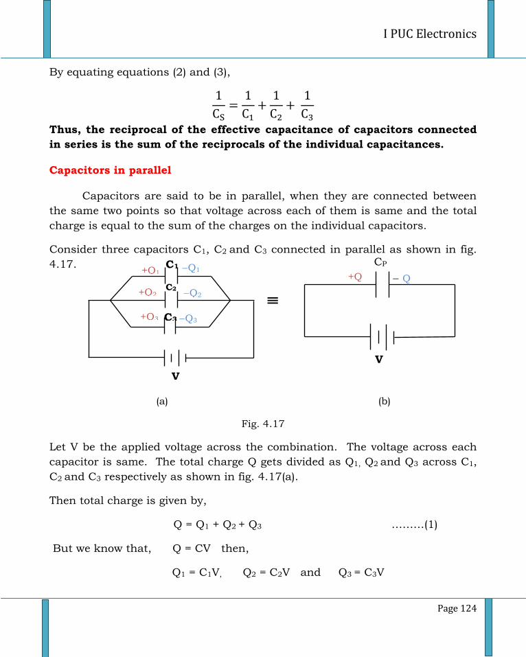
I PUC Electronics
Page 124
By equating equations (2) and (3),
Thus, the reciprocal of the effective capacitance of capacitors connected
in series is the sum of the reciprocals of the individual capacitances.
Capacitors in parallel
Capacitors are said to be in parallel, when they are connected between
the same two points so that voltage across each of them is same and the total
charge is equal to the sum of the charges on the individual capacitors.
Consider three capacitors C1, C2 and C3 connected in parallel as shown in fig.
4.17.
(a) (b)
Fig. 4.17
Let V be the applied voltage across the combination. The voltage across each
capacitor is same. The total charge Q gets divided as Q1, Q2 and Q3 across C1,
C2 and C3 respectively as shown in fig. 4.17(a).
Then total charge is given by,
Q = Q1 + Q2 + Q3 ………(1)
But we know that, Q = CV then,
Q1 = C1V, Q2 = C2V and Q3 = C3V
≡
Q
+Q
V
CP
V
V
+Q1
C1
+Q2
+Q3
Q2
Q1
Q3
C3
C2
Ch-4: Passive Electronic Components
Page 125
Substitute the above values in equation (1), then
Q = C1V + C2V + C3V
= (C1 + C2 + C3) ……… (2)
Cp is the effective capacitance of capacitances C1, C2 and C3. Let the
combination be replaced by an equivalent capacitance Cp with same applied
voltage V and stores charge Q = Q1 + Q2 + Q3 as shown in fig. 4.17(b). Then,
Cp =
……… (3)
From (2) and (3) we get,
CP = C1 + C2 + C3
Thus, the effective capacitance of capacitors in parallel is equal to the
sum of the individual capacitances.
Trouble shooting in capacitors
Generally the troubles in capacitors are open, short, leakage of current and
resistance.
For a good condenser resistance is high at the range of MΩ. An open capacitor
has infinite resistance and a short circuited condenser has zero resistance.
Leakage current and leakage resistance: An ideal condenser holds
the charge given to it for infinite time. But in a practical condenser, electrons
leak through the dielectric from the negative to positive plate. This results in a
small leakage current through the dielectric.
The resistance offered by the dielectric material to the flow of leakage current is
called leakage resistance.
Ageing factors: Use of capacitors over a long period may deteriorate the
dielectric medium which results in decrease in the value of capacitance.
I PUC Electronics
Page 126
Worked example
1. Determine the charge on a 20 µF capacitor charged to 18 volt
Solution:
Given C = 20 µF and VC = 18 volt
We know that, Q = CVC
= 20 x 10-6 x 18 = 360 x 10-6 = 360 µC
2. Two capacitor plates each of effective area 6 x 10⁻⁴ m2 are separated by
1.3 x10⁻³ meter. Find its capacitance. The space between the plates is
filled with air.
Solution:
We know that,
=
= 40.86 x 10⁻¹³
C = 4.086 x 10-12 = 4.086 pF
3. How much energy is stored in a 30 µF capacitor with 12 V across its
plates?
Solution:
We know that energy stored in capacitor is given by,
C
=
× 30 × 10-6 × 122
E = 2160 x 10-6 = 2160 µJ
4. Calculate the total capacitances of three capacitors of 10 µF, 20 µF and 30
µF connected in series.
Ch-4: Passive Electronic Components
Page 127
Solution:
The total effective capacitance is given by,
CS = 5.45 µF.
5. The capacitors of 0.001 µF, 0.002 µF and 0.005 µF are connected in parallel.
Calculate the effective capacitance.
Solution:
The total effective capacitance is given by,
CP = C1 + C2 + C3
= (0.001 + 0.002 + 0.005) x 10-6
CP = 0.008 µF.
6. Determine the effective capacitance of the combination shown in fig. below.
Solution:
Total capacitance between A and B is given by,
CAB = 30 + 30
= 60 µF
Total capacitance between B and C is given by,
CBC = 20 + 20 + 20
CBC = 60 µF
Total capacitance between A and C is given by,
CAC = 30 µF.
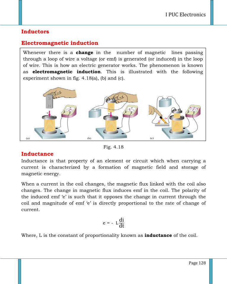
I PUC Electronics
Page 128
Inductors
Electromagnetic induction
Fig. 4.18
Inductance
Inductance is that property of an element or circuit which when carrying a
current is characterized by a formation of magnetic field and storage of
magnetic energy.
When a current in the coil changes, the magnetic flux linked with the coil also
changes. The change in magnetic flux induces emf in the coil. The polarity of
the induced emf ‘e’ is such that it opposes the change in current through the
coil and magnitude of emf ‘e’ is directly proportional to the rate of change of
current.
e = -
Where, L is the constant of proportionality known as inductance of the coil.
Whenever there is a change in the number of magnetic lines passing
through a loop of wire a voltage (or emf) is generated (or induced) in the loop
of wire. This is how an electric generator works. The phenomenon is known
as electromagnetic induction. This is illustrated with the following
experiment shown in fig. 4.18(a), (b) and (c).
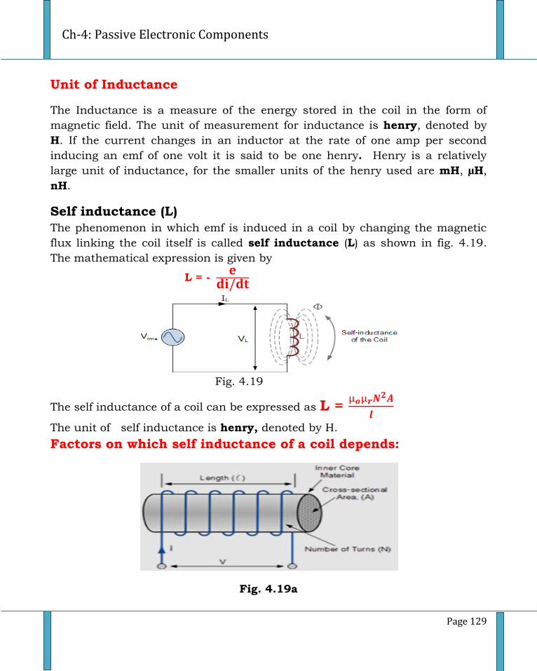
Ch-4: Passive Electronic Components
Page 129
Unit of Inductance
The Inductance is a measure of the energy stored in the coil in the form of
magnetic field. The unit of measurement for inductance is henry, denoted by
H. If the current changes in an inductor at the rate of one amp per second
inducing an emf of one volt it is said to be one henry. Henry is a relatively
large unit of inductance, for the smaller units of the henry used are mH, µH,
nH.
Self inductance (L)
The phenomenon in which emf is induced in a coil by changing the magnetic
flux linking the coil itself is called self inductance (L) as shown in fig. 4.19.
The mathematical expression is given by
L = -
Fig. 4.19
The self inductance of a coil can be expressed as L =
The unit of self inductance is henry, denoted by H.
Factors on which self inductance of a coil depends:
Fig. 4.19a
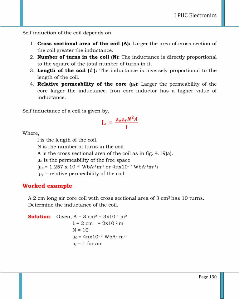
I PUC Electronics
Page 130
Self induction of the coil depends on
1. Cross sectional area of the coil (A): Larger the area of cross section of
the coil greater the inductance.
2. Number of turns in the coil (N): The inductance is directly proportional
to the square of the total number of turns in it.
3. Length of the coil (l ): The inductance is inversely proportional to the
length of the coil.
4. Relative permeability of the core (µr): Larger the permeability of the
core larger the inductance. Iron core inductor has a higher value of
inductance.
Self inductance of a coil is given by,
L =
Where,
l is the length of the coil.
N is the number of turns in the coil
A is the cross sectional area of the coil as in fig. 4.19(a).
µo is the permeability of the free space
(µo = 1.257 x 10 -6 WbA-1m-1 or 4πx10- 7 WbA-1m-1)
µr = relative permeability of the coil
Worked example
A 2 cm long air core coil with cross sectional area of 3 cm2 has 10 turns.
Determine the inductance of the coil.
Solution: Given, A = 3 cm2 = 3x10⁻⁴ m2
ℓ = 2 cm = 2x10⁻² m
N = 10
µ0 = 4πx10- 7 WbA-1m-1
µr = 1 for air
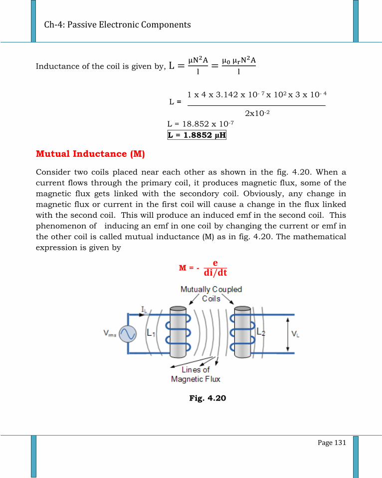
Ch-4: Passive Electronic Components
Page 131
Inductance of the coil is given by,
L = 18.852 x 10⁻⁷
L = 1.8852 µH
Mutual Inductance (M)
Consider two coils placed near each other as shown in the fig. 4.20. When a
current flows through the primary coil, it produces magnetic flux, some of the
magnetic flux gets linked with the secondory coil. Obviously, any change in
magnetic flux or current in the first coil will cause a change in the flux linked
with the second coil. This will produce an induced emf in the second coil. This
phenomenon of inducing an emf in one coil by changing the current or emf in
the other coil is called mutual inductance (M) as in fig. 4.20. The mathematical
expression is given by
M = -
Fig. 4.20
1 x 4 x 3.142 x 10- 7 x 102 x 3 x 10- 4
2x10⁻²
L =
I PUC Electronics
Page 132
Mutual inductance of a coil can be expressed as
M =
Where,
l is the length of the coil
N1 and N2 are the number of turns in the coils L1 and L2
µo is the permeability of the free space
(µo = 1.257 x 10 -6 WbA-1m-1 or 4π x 10- 7 WbA-1m-1)
µr = relative permeability of the coil
A = Area of cross section of core
The unit of mutual inductance is also henry, denoted by H.
Worked example:
An iron core of length 20 cm and area of cross section 3 cm2 is wound with a
coil of 200 turns. Over this coil is wound another coil of 250 turns. The relative
permeability of iron is 800. Determine the mutual inductance between the two
coils.
Solution: Given A = 3 cm2 = 3 x 10- 4 m2, ℓ = 20 cm = 20 x 10-2 m, N1 = 200,
N2 = 250, µ0 = 4π x 10-7 Wb/Am and µr = 800 for Iron
Mutual Inductance of the coil, M =
M = 75.4 mH
Inductor
An Inductor is a coil of copper wire wound on a core of some suitable material.
Inductor opposes the current whenever there is a change in current through it.
However, the opposition offered by an inductor is different for AC and DC
4 x 3.142 x 10- 7 x 800 x 200 x 250 x 3 x 10- 4
20 x 10-2
M =
Ch-4: Passive Electronic Components
Page 133
circuits. In DC they offer almost no impedance because there is no change in
current and they offer high impedance in AC because there is a change in
current.
It is manufactured with a specified amount of inductance, having a core made
up of iron or the other magnetic materials because these materials intensify the
magnetic field. Inductors may also be called as chokes or coils. Electromagnetic
induction is the basic concept for an inductor operation.
The symbol of an inductor is shown in fig. 4.21.
Fig. 4.21
Specification of an inductor
Value of the inductance
Type of the core used
Range of frequencies for which the inductors may be used
Arrangement of the winding
Energy stored in an Inductor
In inductors, due to the change in the current the work will be done and energy
is stored in the magnetic field as magnetic energy. The energy stored is given
by the relation,
E =
L I² joule.
Worked example
Find the energy stored in a 5H inductor when a current of a 6 mA is flowing
through it.
Solution: Given L = 5 H
I = 6 mA = 6 x 10⁻³ A
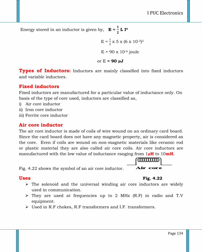
I PUC Electronics
Page 134
Energy stored in an inductor is given by, E =
L I²
E =
x 5 x (6 x 10-3)2
E = 90 x 10-6 joule
or E = 90 µJ
Types of Inductors: Inductors are mainly classified into fixed inductors
and variable inductors.
Fixed inductors
Fixed inductors are manufactured for a particular value of inductance only. On
basis of the type of core used, inductors are classified as,
i) Air core inductor
ii) Iron core inductor
iii) Ferrite core inductor
Air core inductor
The air core inductor is made of coils of wire wound on an ordinary card board.
Since the card board does not have any magnetic property, air is considered as
the core. Even if coils are wound on non-magnetic materials like ceramic rod
or plastic material they are also called air core coils. Air core inductors are
manufactured with the low value of inductance ranging from 1µH to 10mH.
Fig. 4.22 shows the symbol of an air core inductor.
Uses Fig. 4.22
The solenoid and the universal winding air core inductors are widely
used in communication.
They are used at frequencies up to 2 MHz (R.F) in radio and T.V
equipment.
Used in R.F chokes, R.F transformers and I.F. transformers.
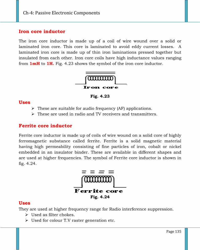
Ch-4: Passive Electronic Components
Page 135
Iron core inductor
The iron core inductor is made up of a coil of wire wound over a solid or
laminated iron core. This core is laminated to avoid eddy current losses. A
laminated iron core is made up of thin iron laminations pressed together but
insulated from each other. Iron core coils have high inductance values ranging
from 1mH to 1H. Fig. 4.23 shows the symbol of the iron core inductor.
Fig. 4.23
Uses
These are suitable for audio frequency (AF) applications.
These are used in radio and TV receivers and transmitters.
Ferrite core inductor
Ferrite core inductor is made up of coils of wire wound on a solid core of highly
ferromagnetic substance called ferrite. Ferrite is a solid magnetic material
having high permeability consisting of fine particles of iron, cobalt or nickel
embedded in an insulator binder. These are available in different shapes and
are used at higher frequencies. The symbol of Ferrite core inductor is shown in
fig. 4.24.
Fig. 4.24
Uses
They are used at higher frequency range for Radio interference suppression.
Used as filter chokes.
Used for colour T.V raster generation etc.
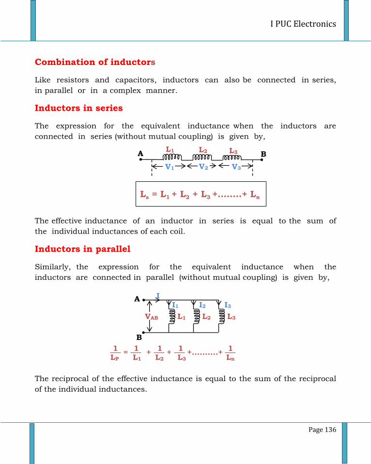
I PUC Electronics
Page 136
Combination of inductors
Like resistors and capacitors, inductors can also be connected in series,
in parallel or in a complex manner.
Inductors in series
The expression for the equivalent inductance when the inductors are
connected in series (without mutual coupling) is given by,
The effective inductance of an inductor in series is equal to the sum of
the individual inductances of each coil.
Inductors in parallel
Similarly, the expression for the equivalent inductance when the
inductors are connected in parallel (without mutual coupling) is given by,
The reciprocal of the effective inductance is equal to the sum of the reciprocal
of the individual inductances.
L1
L2 L3
A
B
I1
I3
I2
I
VAB
1 1 1 1 1 LP L1 L2 L3 Ln
= + + +..........+
Ls = L1 + L2 + L3 +……..+ Ln
L2 L1 A
V1
L3 B
V2 V3
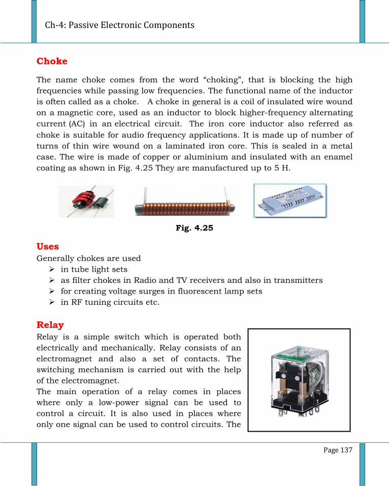
Ch-4: Passive Electronic Components
Page 137
Choke
The name choke comes from the word “choking”, that is blocking the high
frequencies while passing low frequencies. The functional name of the inductor
is often called as a choke. A choke in general is a coil of insulated wire wound
on a magnetic core, used as an inductor to block higher-frequency alternating
current (AC) in an electrical circuit. The iron core inductor also referred as
choke is suitable for audio frequency applications. It is made up of number of
turns of thin wire wound on a laminated iron core. This is sealed in a metal
case. The wire is made of copper or aluminium and insulated with an enamel
coating as shown in Fig. 4.25 They are manufactured up to 5 H.
Fig. 4.25
Uses
Generally chokes are used
in tube light sets
as filter chokes in Radio and TV receivers and also in transmitters
for creating voltage surges in fluorescent lamp sets
in RF tuning circuits etc.
Relay
Relay is a simple switch which is operated both
electrically and mechanically. Relay consists of an
electromagnet and also a set of contacts. The
switching mechanism is carried out with the help
of the electromagnet.
The main operation of a relay comes in places
where only a low-power signal can be used to
control a circuit. It is also used in places where
only one signal can be used to control circuits. The
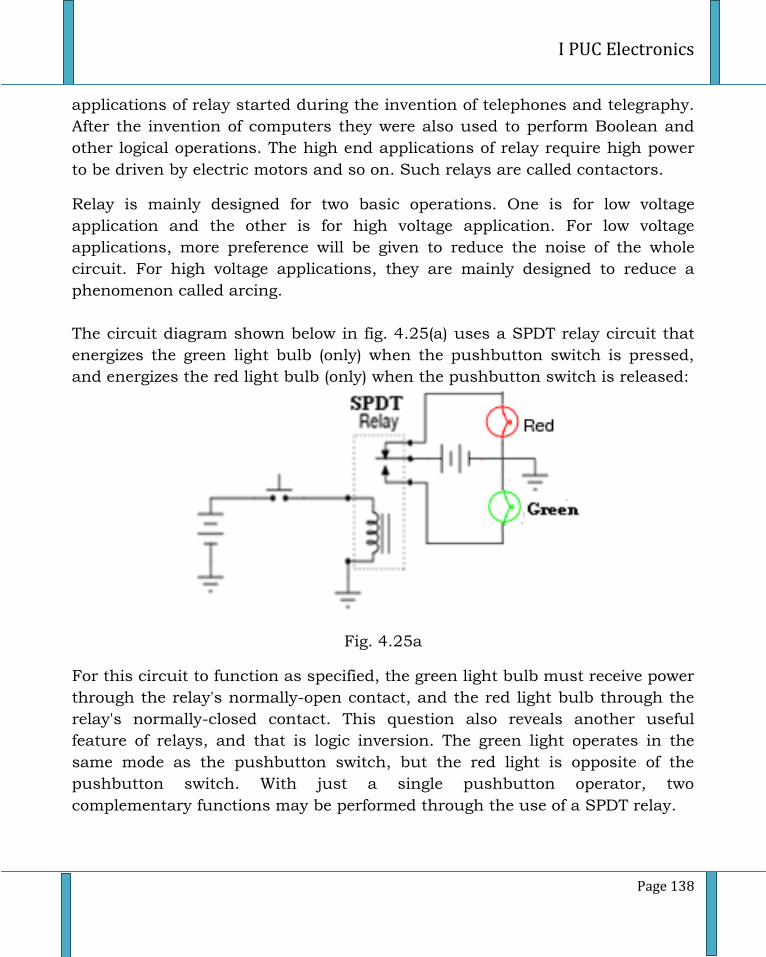
I PUC Electronics
Page 138
applications of relay started during the invention of telephones and telegraphy.
After the invention of computers they were also used to perform Boolean and
other logical operations. The high end applications of relay require high power
to be driven by electric motors and so on. Such relays are called contactors.
Relay is mainly designed for two basic operations. One is for low voltage
application and the other is for high voltage application. For low voltage
applications, more preference will be given to reduce the noise of the whole
circuit. For high voltage applications, they are mainly designed to reduce a
phenomenon called arcing.
The circuit diagram shown below in fig. 4.25(a) uses a SPDT relay circuit that
energizes the green light bulb (only) when the pushbutton switch is pressed,
and energizes the red light bulb (only) when the pushbutton switch is released:
Fig. 4.25a
For this circuit to function as specified, the green light bulb must receive power
through the relay's normally-open contact, and the red light bulb through the
relay's normally-closed contact. This question also reveals another useful
feature of relays, and that is logic inversion. The green light operates in the
same mode as the pushbutton switch, but the red light is opposite of the
pushbutton switch. With just a single pushbutton operator, two
complementary functions may be performed through the use of a SPDT relay.
Ch-4: Passive Electronic Components
Page 139
Specifications of Relay
The important characteristics of relay are,
i) Operating voltage
ii) Operating current
iii) Contact and release time
iv) Material of the Contact point
v) Operating temperature
Application of Relays
They are used,
1. As protective Relay to protect electronic equipments against abnormal
conditions like over voltage, over current, short circuit etc.
2. As transmission Relay in communication systems to generate and
transmit signals.
3. As counters for counting entry into a place.
4. As an automatic switching device to operate street lights, garage doors,
inverters (UPS), bells and buzzers, abnormal conditions like fire, smoke,
theft etc.
Advantages of Relays
Relay, in general have the following advantages.
1. Relay requires small power for its operation to control high power circuit
which acts as a power amplifier.
2. Load can be turned ON/OFF from a distance and hence the operator is
safe from high voltages.
3. There is no sparking while turning the load ON and OFF, as the Relay
coil switch carries low current.
Transformer
A transformer is a power converter that transfers electrical energy from one
circuit to another through coupled conductors. The transformer works on the
principle of mutual induction. It converts high voltage of low current into low
voltage of high current and vice versa. A varying current in the primary
winding creates a varying magnetic flux in the core of the transformer which
I PUC Electronics
Page 140
results in varying magnetic field through the secondary winding. This varying
magnetic field induces an electromotive force (EMF) or voltage in the secondary
winding. This is called mutual coupling.
Fig. 4.26
Transformer consists of two coils called primary and secondary coil as shown
in fig.4.26. The primary coil is connected to a voltage source that produces an
alternating current, while secondary coil is connected across the load. The
coils are electrically separated but the power in the primary coil is coupled into
the secondary coil.
Voltage/current transformation ratio
The induced voltage in the secondary winding (Vs) is in proportion to the
primary voltage (Vp) and is given by the ratio of the number of turns in the
secondary (Ns) to the number of turns in the primary (Np) as given below:
=
Ns/Np is known as the turn’s ratio (T) of a transformer. For example, a
transformer with primary and secondary windings of 100 and 150 turns is said
to have a turn ratio of 2:3.
A transformer with various voltages, currents and turns are shown in fig. 4.27.
Ch-4: Passive Electronic Components
Page 141
Fig. 4.27
When the secondary coil is connected to a load, the current flows so that
electrical power is transmitted from the primary to the secondary. For an ideal
transformer, input power P in is equal to the output power Pout.
From the above equation, the ratio of secondary voltage to the primary voltage
is known as the voltage ratio and current ratio is defined as the ratio of
primary current to the secondary current.
By proper selection of the ratio of number of turns of the coil, a transformer
enables an ac voltage to be stepped up by making Ns greater than Np (i.e., Ns >
Np) known as step up transformer and stepped down by making Ns less than
Np (i.e., Ns < Np) known as step down transformer.
In certain applications transformer with centre-tapping is necessary in which
the secondary winding is exactly tapped at the centre as shown in fig. 4.28. In
such case, secondary voltages with respect to centre tap is equal and opposite.
i.e., VA = - VB.
Vs Ns IP VP Np Is
= =
Pin = VPIP = Pout = VSIS
I PUC Electronics
Page 142
Fig.4.28
Applications of transformers
Transformers are used
to step-up or step-down ac voltage or current.
to act as an impedance matching device.
to electrically isolate one portion of a circuit from the other.
in home appliances, lights, industrial machineries and other electric
equipment.
in TV, Radio and Telephones.
in power stations, etc.
Efficiency ()
Efficiency of a transformer is defined as the ratio of output power to the input
power expressed in percentage. It normally ranges from 90% to 95%.
Types of Transformers
Power Transformer (PT) - Designed to operate in ac mains frequency (50
Hz or 60 Hz).
Audio Frequency Transformer (AFT) - Designed to operate in audio
frequency range (20 Hz to 20 KHz).
Radio Frequency Transformer (RFT) - Designed to operate in radio
frequency range (550 KHz to 1650 KHz).
Output power (Pout )
Input power ( Pin ) Efficiency () = X 100
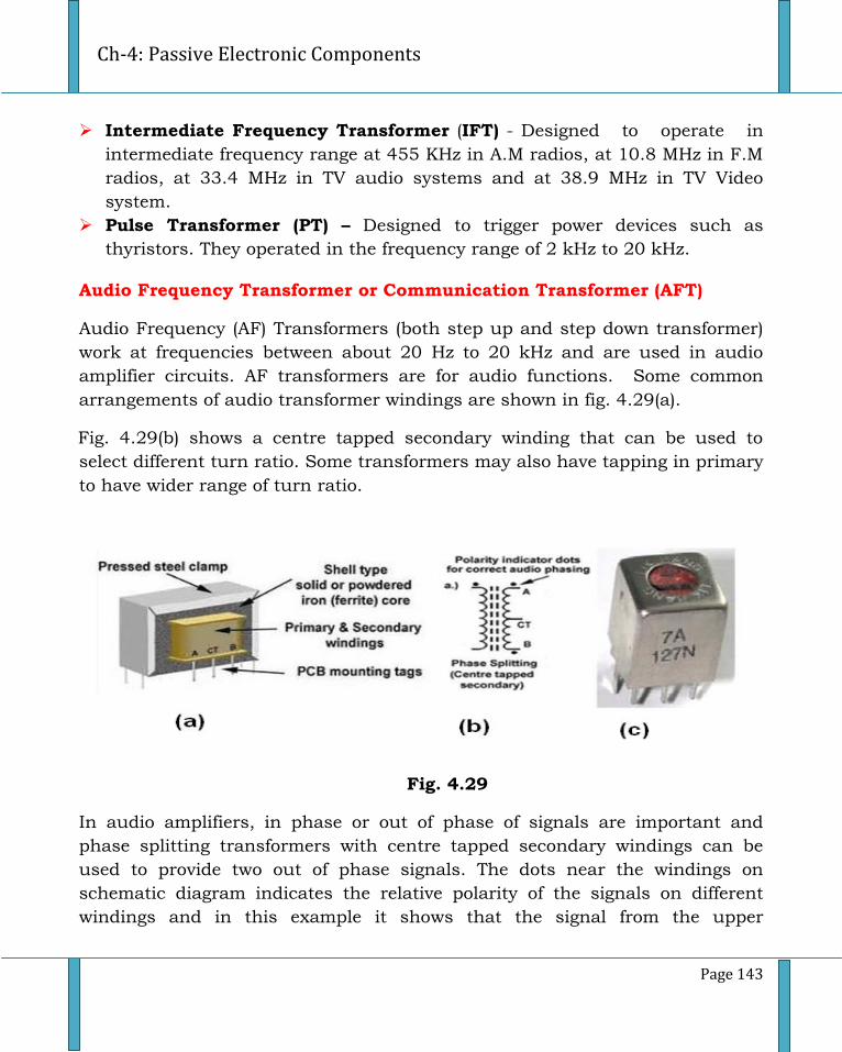
Ch-4: Passive Electronic Components
Page 143
Intermediate Frequency Transformer (IFT) - Designed to operate in
intermediate frequency range at 455 KHz in A.M radios, at 10.8 MHz in F.M
radios, at 33.4 MHz in TV audio systems and at 38.9 MHz in TV Video
system.
Pulse Transformer (PT) – Designed to trigger power devices such as
thyristors. They operated in the frequency range of 2 kHz to 20 kHz.
Audio Frequency Transformer or Communication Transformer (AFT)
Audio Frequency (AF) Transformers (both step up and step down transformer)
work at frequencies between about 20 Hz to 20 kHz and are used in audio
amplifier circuits. AF transformers are for audio functions. Some common
arrangements of audio transformer windings are shown in fig. 4.29(a).
Fig. 4.29(b) shows a centre tapped secondary winding that can be used to
select different turn ratio. Some transformers may also have tapping in primary
to have wider range of turn ratio.
Fig. 4.29
In audio amplifiers, in phase or out of phase of signals are important and
phase splitting transformers with centre tapped secondary windings can be
used to provide two out of phase signals. The dots near the windings on
schematic diagram indicates the relative polarity of the signals on different
windings and in this example it shows that the signal from the upper
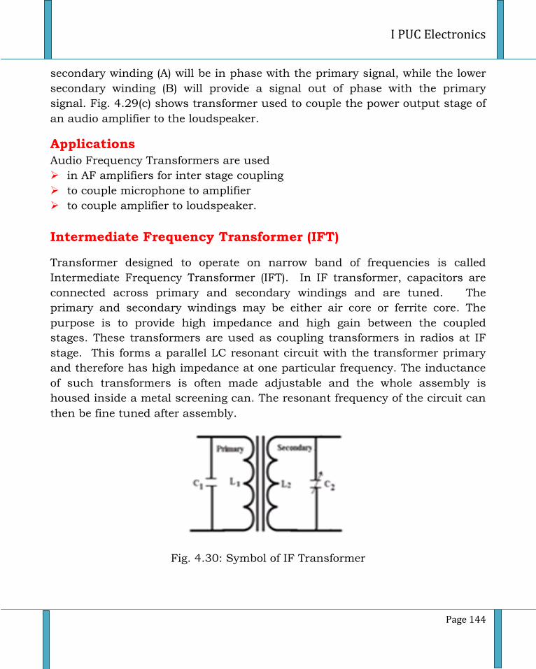
I PUC Electronics
Page 144
secondary winding (A) will be in phase with the primary signal, while the lower
secondary winding (B) will provide a signal out of phase with the primary
signal. Fig. 4.29(c) shows transformer used to couple the power output stage of
an audio amplifier to the loudspeaker.
Applications
Audio Frequency Transformers are used
in AF amplifiers for inter stage coupling
to couple microphone to amplifier
to couple amplifier to loudspeaker.
Intermediate Frequency Transformer (IFT)
Transformer designed to operate on narrow band of frequencies is called
Intermediate Frequency Transformer (IFT). In IF transformer, capacitors are
connected across primary and secondary windings and are tuned. The
primary and secondary windings may be either air core or ferrite core. The
purpose is to provide high impedance and high gain between the coupled
stages. These transformers are used as coupling transformers in radios at IF
stage. This forms a parallel LC resonant circuit with the transformer primary
and therefore has high impedance at one particular frequency. The inductance
of such transformers is often made adjustable and the whole assembly is
housed inside a metal screening can. The resonant frequency of the circuit can
then be fine tuned after assembly.
Fig. 4.30: Symbol of IF Transformer
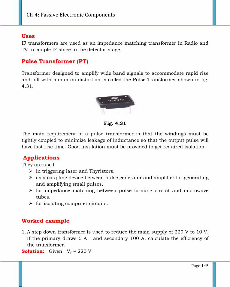
Ch-4: Passive Electronic Components
Page 145
Uses
IF transformers are used as an impedance matching transformer in Radio and
TV to couple IF stage to the detector stage.
Pulse Transformer (PT)
Transformer designed to amplify wide band signals to accommodate rapid rise
and fall with minimum distortion is called the Pulse Transformer shown in fig.
4.31.
Fig. 4.31
The main requirement of a pulse transformer is that the windings must be
tightly coupled to minimize leakage of inductance so that the output pulse will
have fast rise time. Good insulation must be provided to get required isolation.
Applications
They are used
in triggering laser and Thyristors.
as a coupling device between pulse generator and amplifier for generating
and amplifying small pulses.
for impedance matching between pulse forming circuit and microwave
tubes.
for isolating computer circuits.
Worked example
1. A step down transformer is used to reduce the main supply of 220 V to 10 V.
If the primary draws 5 A and secondary 100 A, calculate the efficiency of
the transformer.
Solution: Given Vp = 220 V
I PUC Electronics
Page 146
Vs = 10 V
Ip = 5 A
Is = 100 A
We know that Pout = Vs X Is = 10 X 100 = 1000 W
Similarly, Pin = Vp X Ip = 220 X 5 = 1100 W
Efficiency of the transformer is given by =
X 100 = 91%
Transducer
Transducer is a device which converts one form of energy into another. Energy
may be electrical, mechanical, pressure, chemical, optical or thermal etc.
Transducer may be classified according to their applications, method of energy
conversion and nature of the output signal and so on.
Selecting a transducer
The transducer has to be physically compatible with its intended applications.
To select a transducer, there are eight parameters to be considered, they are,
1. Operating range
2. Sensitivity
3. Frequency response and resonant frequency
4. Environmental compatibility
5. Minimum sensitivity
6. Accuracy
7. Usage and ruggedness
8. Electrical characteristics
Pressure transducers
A device that converts pressure variation into electrical signals, likewise it can
also convert electrical signal into pressure variation. Microphone and Loud
speaker are the two common examples of pressure transducer.
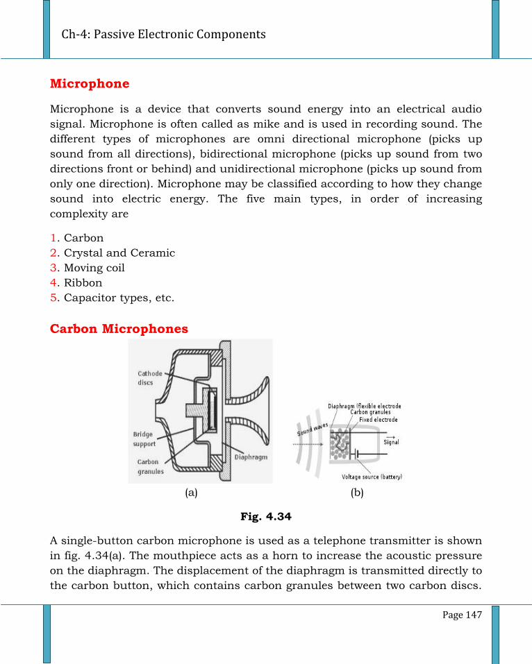
Ch-4: Passive Electronic Components
Page 147
Microphone
Microphone is a device that converts sound energy into an electrical audio
signal. Microphone is often called as mike and is used in recording sound. The
different types of microphones are omni directional microphone (picks up
sound from all directions), bidirectional microphone (picks up sound from two
directions front or behind) and unidirectional microphone (picks up sound from
only one direction). Microphone may be classified according to how they change
sound into electric energy. The five main types, in order of increasing
complexity are
1. Carbon
2. Crystal and Ceramic
3. Moving coil
4. Ribbon
5. Capacitor types, etc.
Carbon Microphones
(a) (b)
Fig. 4.34
A single-button carbon microphone is used as a telephone transmitter is shown
in fig. 4.34(a). The mouthpiece acts as a horn to increase the acoustic pressure
on the diaphragm. The displacement of the diaphragm is transmitted directly to
the carbon button, which contains carbon granules between two carbon discs.
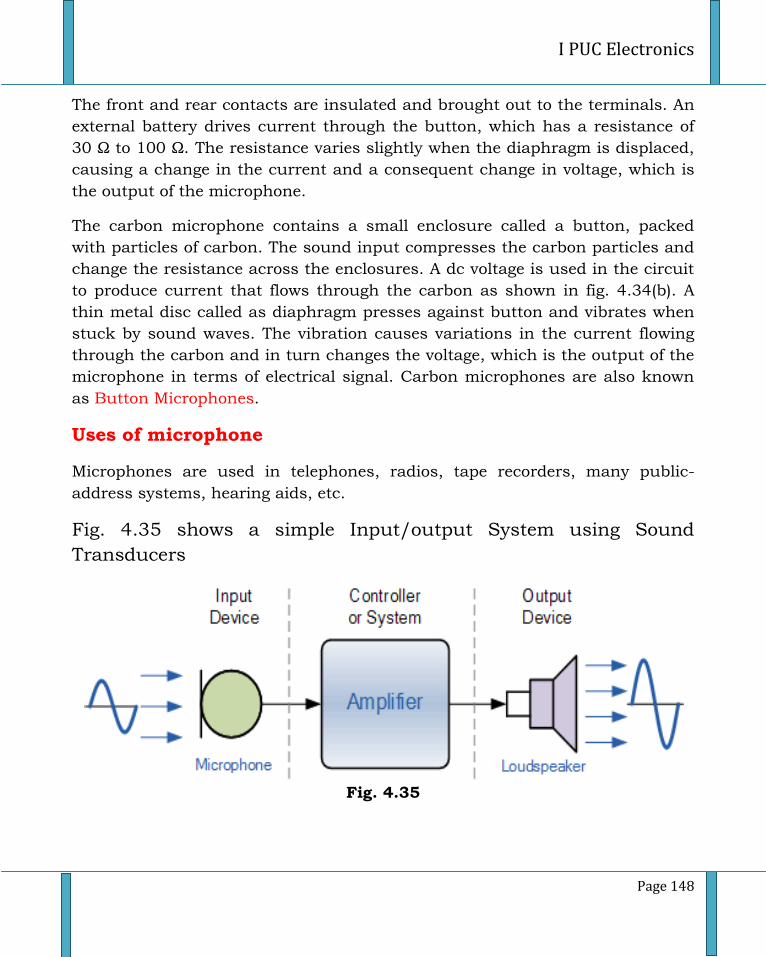
I PUC Electronics
Page 148
The front and rear contacts are insulated and brought out to the terminals. An
external battery drives current through the button, which has a resistance of
30 Ω to 100 Ω. The resistance varies slightly when the diaphragm is displaced,
causing a change in the current and a consequent change in voltage, which is
the output of the microphone.
The carbon microphone contains a small enclosure called a button, packed
with particles of carbon. The sound input compresses the carbon particles and
change the resistance across the enclosures. A dc voltage is used in the circuit
to produce current that flows through the carbon as shown in fig. 4.34(b). A
thin metal disc called as diaphragm presses against button and vibrates when
stuck by sound waves. The vibration causes variations in the current flowing
through the carbon and in turn changes the voltage, which is the output of the
microphone in terms of electrical signal. Carbon microphones are also known
as Button Microphones.
Uses of microphone
Microphones are used in telephones, radios, tape recorders, many public-
address systems, hearing aids, etc.
Fig. 4.35 shows a simple Input/output System using Sound
Transducers
Fig. 4.35
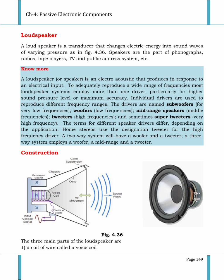
Ch-4: Passive Electronic Components
Page 149
Loudspeaker
A loud speaker is a transducer that changes electric energy into sound waves
of varying pressure as in fig. 4.36. Speakers are the part of phonographs,
radios, tape players, TV and public address system, etc.
Know more
A loudspeaker (or speaker) is an electro acoustic that produces in response to
an electrical input. To adequately reproduce a wide range of frequencies most
loudspeaker systems employ more than one driver, particularly for higher
sound pressure level or maximum accuracy. Individual drivers are used to
reproduce different frequency ranges. The drivers are named subwoofers (for
very low frequencies); woofers (low frequencies); mid-range speakers (middle
frequencies); tweeters (high frequencies); and sometimes super tweeters (very
high frequency). The terms for different speaker drivers differ, depending on
the application. Home stereos use the designation tweeter for the high
frequency driver. A two-way system will have a woofer and a tweeter; a three-
way system employs a woofer, a mid-range and a tweeter.
Construction
Fig. 4.36
The three main parts of the loudspeaker are
1) a coil of wire called a voice coil
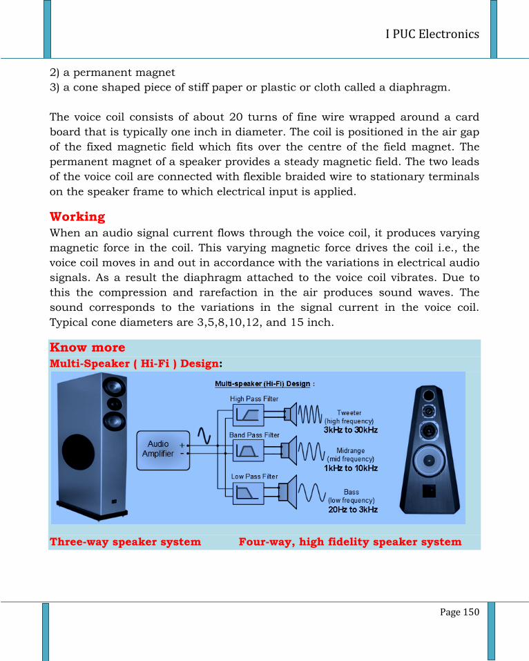
I PUC Electronics
Page 150
2) a permanent magnet
3) a cone shaped piece of stiff paper or plastic or cloth called a diaphragm.
The voice coil consists of about 20 turns of fine wire wrapped around a card
board that is typically one inch in diameter. The coil is positioned in the air gap
of the fixed magnetic field which fits over the centre of the field magnet. The
permanent magnet of a speaker provides a steady magnetic field. The two leads
of the voice coil are connected with flexible braided wire to stationary terminals
on the speaker frame to which electrical input is applied.
Working
When an audio signal current flows through the voice coil, it produces varying
magnetic force in the coil. This varying magnetic force drives the coil i.e., the
voice coil moves in and out in accordance with the variations in electrical audio
signals. As a result the diaphragm attached to the voice coil vibrates. Due to
this the compression and rarefaction in the air produces sound waves. The
sound corresponds to the variations in the signal current in the voice coil.
Typical cone diameters are 3,5,8,10,12, and 15 inch.
Know more
Multi-Speaker ( Hi-Fi ) Design:
Three-way speaker system Four-way, high fidelity speaker system
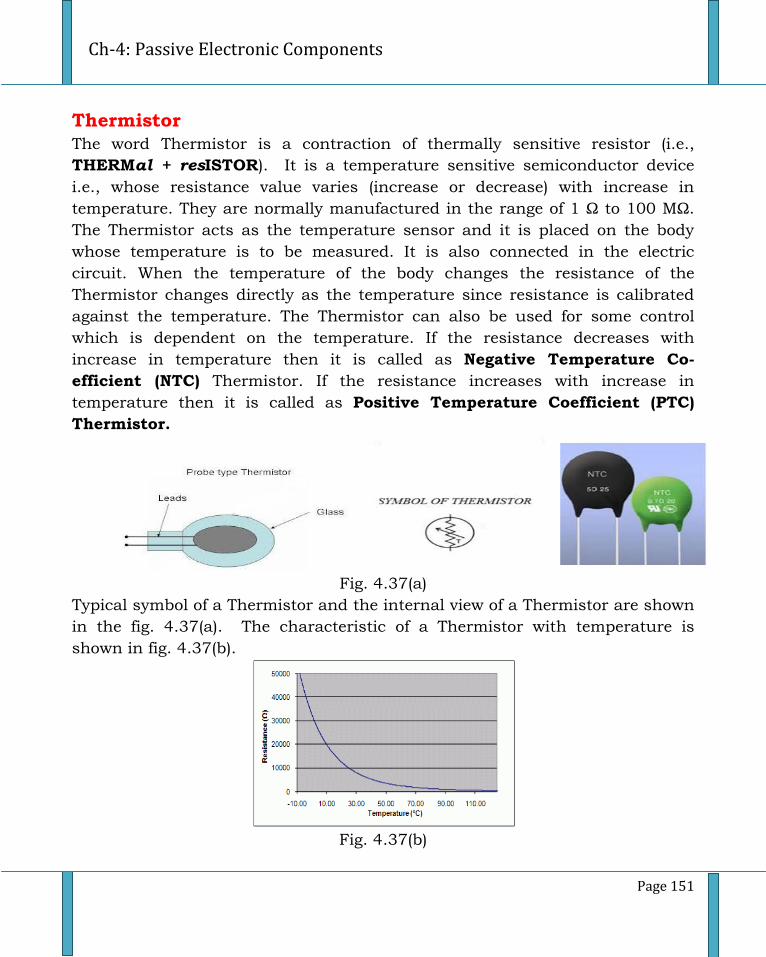
Ch-4: Passive Electronic Components
Page 151
Thermistor
The word Thermistor is a contraction of thermally sensitive resistor (i.e.,
THERMal + resISTOR). It is a temperature sensitive semiconductor device
i.e., whose resistance value varies (increase or decrease) with increase in
temperature. They are normally manufactured in the range of 1 Ω to 100 MΩ.
The Thermistor acts as the temperature sensor and it is placed on the body
whose temperature is to be measured. It is also connected in the electric
circuit. When the temperature of the body changes the resistance of the
Thermistor changes directly as the temperature since resistance is calibrated
against the temperature. The Thermistor can also be used for some control
which is dependent on the temperature. If the resistance decreases with
increase in temperature then it is called as Negative Temperature Co-
efficient (NTC) Thermistor. If the resistance increases with increase in
temperature then it is called as Positive Temperature Coefficient (PTC)
Thermistor.
Fig. 4.37(a)
Typical symbol of a Thermistor and the internal view of a Thermistor are shown
in the fig. 4.37(a). The characteristic of a Thermistor with temperature is
shown in fig. 4.37(b).
Fig. 4.37(b)
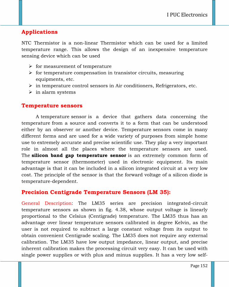
I PUC Electronics
Page 152
Applications
NTC Thermistor is a non-linear Thermistor which can be used for a limited
temperature range. This allows the design of an inexpensive temperature
sensing device which can be used
for measurement of temperature
for temperature compensation in transistor circuits, measuring
equipments, etc.
in temperature control sensors in Air conditioners, Refrigerators, etc.
in alarm systems
Temperature sensors
A temperature sensor is a device that gathers data concerning the
temperature from a source and converts it to a form that can be understood
either by an observer or another device. Temperature sensors come in many
different forms and are used for a wide variety of purposes from simple home
use to extremely accurate and precise scientific use. They play a very important
role in almost all the places where the temperature sensors are used.
The silicon band gap temperature sensor is an extremely common form of
temperature sensor (thermometer) used in electronic equipment. Its main
advantage is that it can be included in a silicon integrated circuit at a very low
cost. The principle of the sensor is that the forward voltage of a silicon diode is
temperature-dependent.
Precision Centigrade Temperature Sensors (LM 35):
General Description: The LM35 series are precision integrated-circuit
temperature sensors as shown in fig. 4.38, whose output voltage is linearly
proportional to the Celsius (Centigrade) temperature. The LM35 thus has an
advantage over linear temperature sensors calibrated in degree Kelvin, as the
user is not required to subtract a large constant voltage from its output to
obtain convenient Centigrade scaling. The LM35 does not require any external
calibration. The LM35 have low output impedance, linear output, and precise
inherent calibration makes the processing circuit very easy. It can be used with
single power supplies or with plus and minus supplies. It has a very low self-
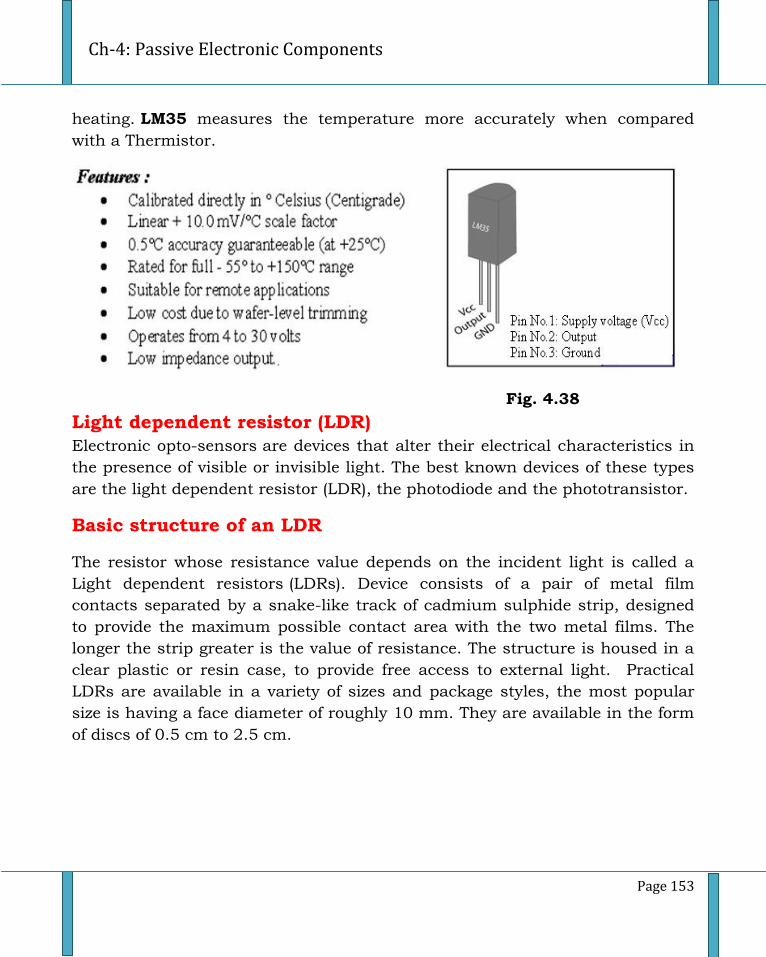
Ch-4: Passive Electronic Components
Page 153
heating. LM35 measures the temperature more accurately when compared
with a Thermistor.
Fig. 4.38
Light dependent resistor (LDR)
Electronic opto-sensors are devices that alter their electrical characteristics in
the presence of visible or invisible light. The best known devices of these types
are the light dependent resistor (LDR), the photodiode and the phototransistor.
Basic structure of an LDR
The resistor whose resistance value depends on the incident light is called a
Light dependent resistors (LDRs). Device consists of a pair of metal film
contacts separated by a snake-like track of cadmium sulphide strip, designed
to provide the maximum possible contact area with the two metal films. The
longer the strip greater is the value of resistance. The structure is housed in a
clear plastic or resin case, to provide free access to external light. Practical
LDRs are available in a variety of sizes and package styles, the most popular
size is having a face diameter of roughly 10 mm. They are available in the form
of discs of 0.5 cm to 2.5 cm.
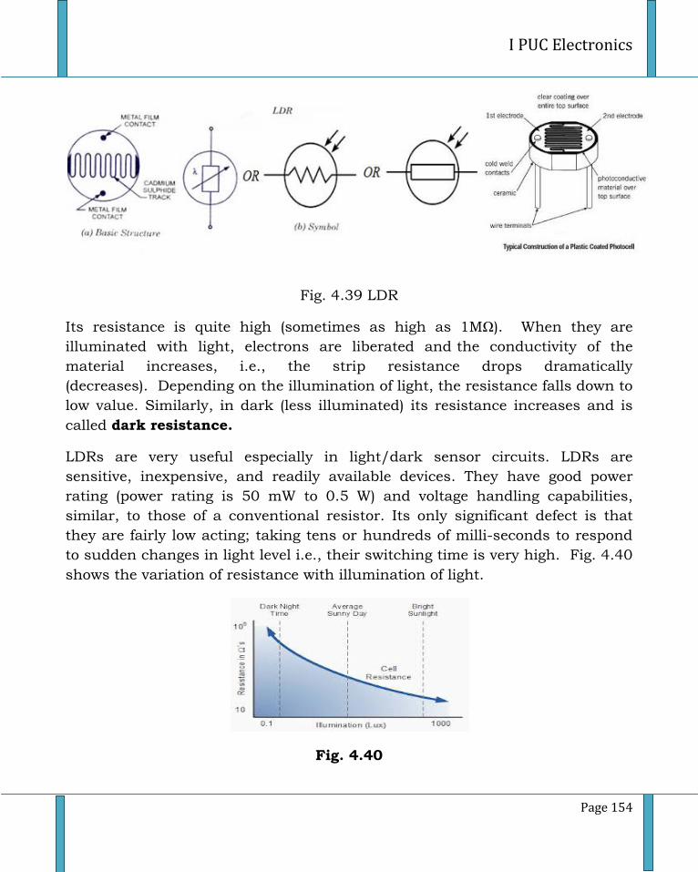
I PUC Electronics
Page 154
Fig. 4.39 LDR
Its resistance is quite high (sometimes as high as 1MΩ). When they are
illuminated with light, electrons are liberated and the conductivity of the
material increases, i.e., the strip resistance drops dramatically
(decreases). Depending on the illumination of light, the resistance falls down to
low value. Similarly, in dark (less illuminated) its resistance increases and is
called dark resistance.
LDRs are very useful especially in light/dark sensor circuits. LDRs are
sensitive, inexpensive, and readily available devices. They have good power
rating (power rating is 50 mW to 0.5 W) and voltage handling capabilities,
similar, to those of a conventional resistor. Its only significant defect is that
they are fairly low acting; taking tens or hundreds of milli-seconds to respond
to sudden changes in light level i.e., their switching time is very high. Fig. 4.40
shows the variation of resistance with illumination of light.
Fig. 4.40
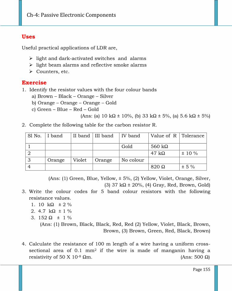
Ch-4: Passive Electronic Components
Page 155
Uses
Useful practical applications of LDR are,
light and dark-activated switches and alarms
light beam alarms and reflective smoke alarms
Counters, etc.
Exercise
1. Identify the resistor values with the four colour bands
a) Brown – Black – Orange – Silver
b) Orange – Orange – Orange – Gold
c) Green – Blue – Red – Gold
(Ans: (a) 10 kΩ ± 10%, (b) 33 kΩ ± 5%, (a) 5.6 kΩ ± 5%)
2. Complete the following table for the carbon resistor R.
Sl No. I band II band III band IV band Value of R Tolerance
1 Gold 560 kΩ
2 47 kΩ ± 10 %
3 Orange Violet Orange No colour
4 820 Ω ± 5 %
(Ans: (1) Green, Blue, Yellow, ± 5%, (2) Yellow, Violet, Orange, Silver,
(3) 37 kΩ ± 20%, (4) Gray, Red, Brown, Gold)
3. Write the colour codes for 5 band colour resistors with the following
resistance values.
1. 10 kΩ ± 2 %
2. 4.7 kΩ ± 1 %
3. 152 Ω ± 1 %
(Ans: (1) Brown, Black, Black, Red, Red (2) Yellow, Violet, Black, Brown,
Brown, (3) Brown, Green, Red, Black, Brown)
4. Calculate the resistance of 100 m length of a wire having a uniform cross-
sectional area of 0.1 mm2 if the wire is made of manganin having a
resistivity of 50 X 10-8 Ωm. (Ans: 500 Ω)
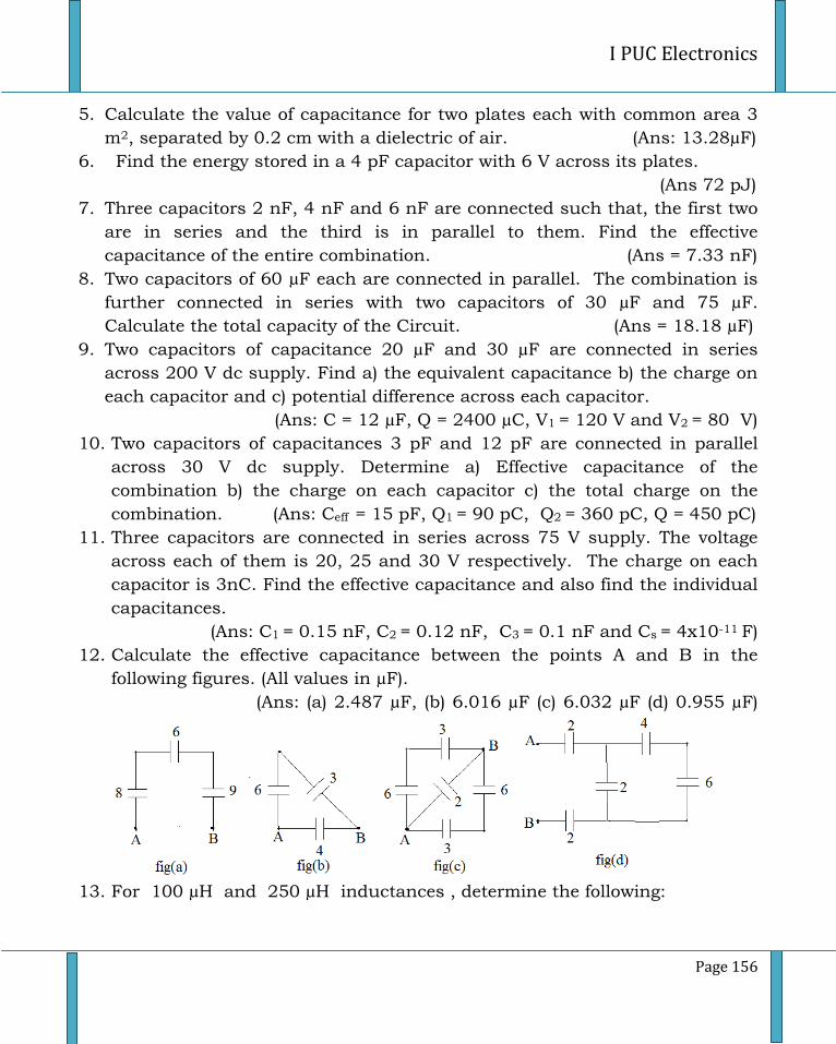
I PUC Electronics
Page 156
5. Calculate the value of capacitance for two plates each with common area 3
m2, separated by 0.2 cm with a dielectric of air. (Ans: 13.28µF)
6. Find the energy stored in a 4 pF capacitor with 6 V across its plates.
(Ans 72 pJ)
7. Three capacitors 2 nF, 4 nF and 6 nF are connected such that, the first two
are in series and the third is in parallel to them. Find the effective
capacitance of the entire combination. (Ans = 7.33 nF)
8. Two capacitors of 60 µF each are connected in parallel. The combination is
further connected in series with two capacitors of 30 µF and 75 µF.
Calculate the total capacity of the Circuit. (Ans = 18.18 µF)
9. Two capacitors of capacitance 20 µF and 30 µF are connected in series
across 200 V dc supply. Find a) the equivalent capacitance b) the charge on
each capacitor and c) potential difference across each capacitor.
(Ans: C = 12 µF, Q = 2400 µC, V1 = 120 V and V2 = 80 V)
10. Two capacitors of capacitances 3 pF and 12 pF are connected in parallel
across 30 V dc supply. Determine a) Effective capacitance of the
combination b) the charge on each capacitor c) the total charge on the
combination. (Ans: Ceff = 15 pF, Q1 = 90 pC, Q2 = 360 pC, Q = 450 pC)
11. Three capacitors are connected in series across 75 V supply. The voltage
across each of them is 20, 25 and 30 V respectively. The charge on each
capacitor is 3nC. Find the effective capacitance and also find the individual
capacitances.
(Ans: C1 = 0.15 nF, C2 = 0.12 nF, C3 = 0.1 nF and Cs = 4x10-11 F)
12. Calculate the effective capacitance between the points A and B in the
following figures. (All values in µF).
(Ans: (a) 2.487 µF, (b) 6.016 µF (c) 6.032 µF (d) 0.955 µF)
13. For 100 µH and 250 µH inductances , determine the following:
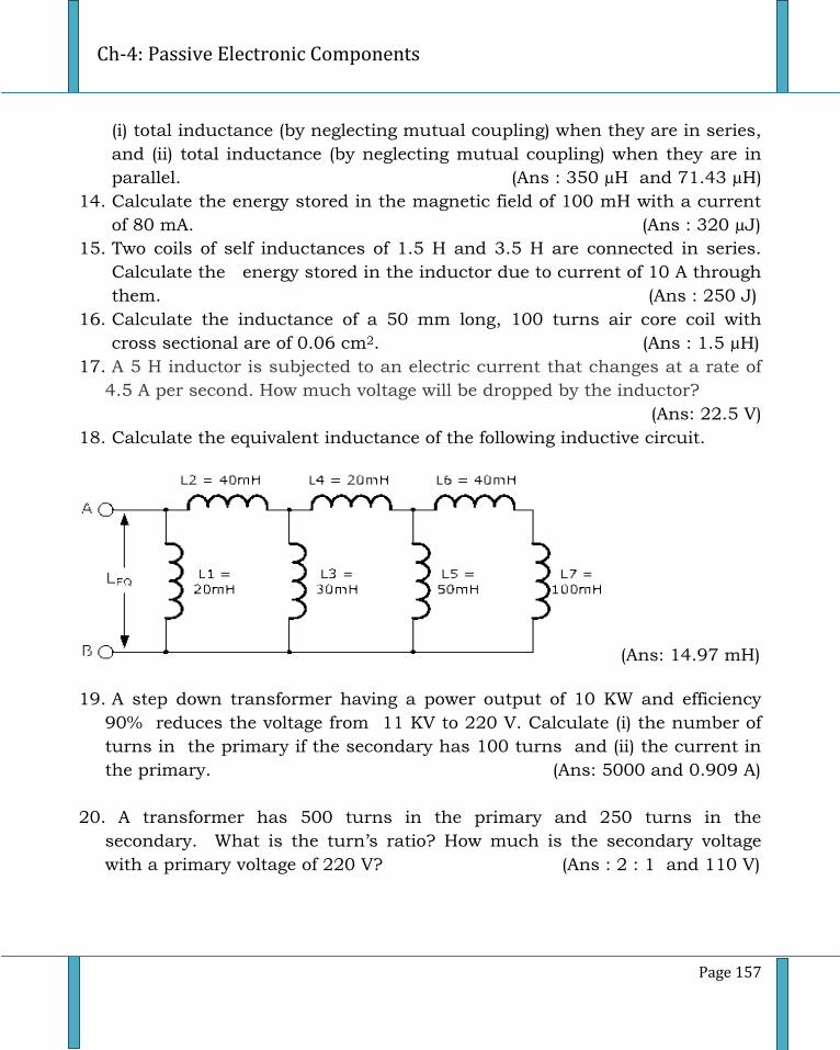
Ch-4: Passive Electronic Components
Page 157
(i) total inductance (by neglecting mutual coupling) when they are in series,
and (ii) total inductance (by neglecting mutual coupling) when they are in
parallel. (Ans : 350 µH and 71.43 µH)
14. Calculate the energy stored in the magnetic field of 100 mH with a current
of 80 mA. (Ans : 320 µJ)
15. Two coils of self inductances of 1.5 H and 3.5 H are connected in series.
Calculate the energy stored in the inductor due to current of 10 A through
them. (Ans : 250 J)
16. Calculate the inductance of a 50 mm long, 100 turns air core coil with
cross sectional are of 0.06 cm2. (Ans : 1.5 µH)
17. A 5 H inductor is subjected to an electric current that changes at a rate of
4.5 A per second. How much voltage will be dropped by the inductor?
(Ans: 22.5 V)
18. Calculate the equivalent inductance of the following inductive circuit.
(Ans: 14.97 mH)
19. A step down transformer having a power output of 10 KW and efficiency
90% reduces the voltage from 11 KV to 220 V. Calculate (i) the number of
turns in the primary if the secondary has 100 turns and (ii) the current in
the primary. (Ans: 5000 and 0.909 A)
20. A transformer has 500 turns in the primary and 250 turns in the
secondary. What is the turn’s ratio? How much is the secondary voltage
with a primary voltage of 220 V? (Ans : 2 : 1 and 110 V)
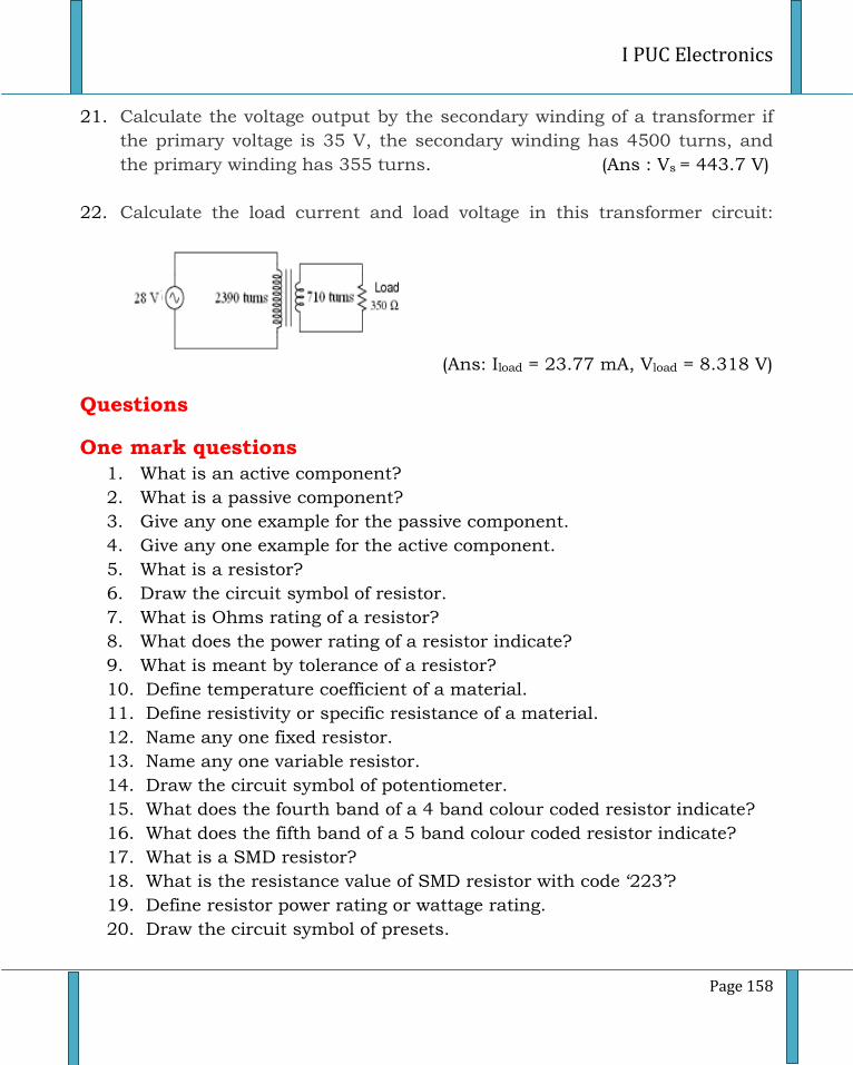
I PUC Electronics
Page 158
21. Calculate the voltage output by the secondary winding of a transformer if
the primary voltage is 35 V, the secondary winding has 4500 turns, and
the primary winding has 355 turns. (Ans : Vs = 443.7 V)
22. Calculate the load current and load voltage in this transformer circuit:
(Ans: Iload = 23.77 mA, Vload = 8.318 V)
Questions
One mark questions
1. What is an active component?
2. What is a passive component?
3. Give any one example for the passive component.
4. Give any one example for the active component.
5. What is a resistor?
6. Draw the circuit symbol of resistor.
7. What is Ohms rating of a resistor?
8. What does the power rating of a resistor indicate?
9. What is meant by tolerance of a resistor?
10. Define temperature coefficient of a material.
11. Define resistivity or specific resistance of a material.
12. Name any one fixed resistor.
13. Name any one variable resistor.
14. Draw the circuit symbol of potentiometer.
15. What does the fourth band of a 4 band colour coded resistor indicate?
16. What does the fifth band of a 5 band colour coded resistor indicate?
17. What is a SMD resistor?
18. What is the resistance value of SMD resistor with code ‘223’?
19. Define resistor power rating or wattage rating.
20. Draw the circuit symbol of presets.
Ch-4: Passive Electronic Components
Page 159
21. What is a capacitor?
22. What is capacitance of a capacitor?
23. What is the S.I unit of capacitance?
24. What is dielectric constant?
25. Draw the symbol of electrolytic capacitor.
26. Write an expression for energy stored in a capacitor.
27. How do you connect number of capacitors to obtain maximum
capacitance value?
28. Which type of capacitor is sensitive to polarity?
29. Write an expression for capacitance of a parallel plate capacitor.
30. What is electromagnetic induction?
31. What is an inductor?
32. What is the unit of inductance?
33. Define unit of inductance.
34. Which has more inductance, a coil with an iron core or with air core?
35. Write an expression for energy stored in an inductor?
36. Write the symbol of inductor.
37. Write the symbol of air core inductor.
38. Write the symbol of iron core inductor.
39. Write the symbol of ferrite core inductor.
40. Write the expression for effective inductance when the inductors are
Connected in series.
41. Write the expression for effective Inductance when the inductors are
connected in parallel.
42. What is choke?
43. What is relay?
44. What is transformer?
45. Define transformer efficiency.
46. Define turns ratio.
47. Write the relation between turns ratio, voltage ratio and current ratio in
a transformer.
48. Write the symbol of transformer.
49. Name the principle of transformer.
50. What is a step up transformer?
51. What is a step down transformer?
I PUC Electronics
Page 160
52. Could step up transformer be used as a step down transformer?
53. What would be the voltage across the secondary of a transformer with
DC voltage across the primary?
54. What is Transducer?
55. What is meant by pressure transducer?
56. What is meant by loud speaker?
57. What is meant by microphone?
58. What is tweeter?
59. What is woofer?
60. Expand NTC.
61. Expand PTC.
62. Define NTC thermistor.
63. Define PTC thermistor.
64. What is meant by thermistor?
65. What is meant by temperature sensors?
66. Write the symbol of thermistor.
67. Give one example for temperature sensor.
68. What for LM 35 is used?
69. What is meant by LDR?
70. Write the symbol of LDR?
Two mark questions
1. Distinguish between active and passive components.
2. Write four important characteristics of resistors.
3. Distinguish between fixed resistor and variable resistor.
4. Write a note on SMD resistor.
5. Write a note on presets.
6. Write a note on power rating of a resistor.
7. Mention the factors on which the capacitance of a capacitor depends.
8. Briefly explain about role of a dielectric in capacitor.
9. Mention any four types of dielectric materials used in capacitors.
10. Write a note on an energy stored in a capacitor.
11. Write a note on leakage current and leakage resistance in capacitor.
12. Name any four types of capacitor.
13. Write a note on trimmers.
Ch-4: Passive Electronic Components
Page 161
14. When an electric current is passed through a coil of wire, what
phenomenon occurs?
15. What is Self - inductance? Explain.
16. What is Mutual - inductance? Explain.
17. List the factors on which self – inductance of a coil depends.
18. List the factors on which mutual – inductance of a pair of coil depends.
19. Distinguish between self inductance and mutual inductance.
20. Write the specifications of an inductor.
21. Name the factors on which inductance of a coil depend.
22. Mention the types of inductors.
23. Explain the construction of air core inductor.
24. Write the applications of air core inductor.
25. Explain the construction of iron core inductor.
26. Write the applications of iron core inductor.
27. Explain the construction of ferrite core inductor.
28. Write the applications of ferrite core inductor.
29. Write the applications of chokes.
30. Write the applications of relays.
31. List the advantages of relays.
32. Explain the principle of a transformer.
33. What are step-up and step-down transformers?
34. Explain how the construction of step-up transformer is differ from
Step down transformers.
35. Mention the different types of transformers.
36. Why there is no voltage across the secondary if the primary is open?
37. Write the application of a transformer.
38. Write the applications of AF transformer.
39. Write the applications of IF transformer.
40. Write the applications of pulse transformer.
41. Explain briefly the construction of pulse transformer.
42. What is the use of centre tap in transformer? Explain.
43. Give the two examples for pressure transducers.
44. Distinguish between tweeter and woofer.
45. Distinguish between speaker and microphone.
46. Write the applications of speaker.
I PUC Electronics
Page 162
47. Write the applications of microphone.
48. Write the applications of thermistor.
49. Draw the pin diagram of LM 35.
50. Write the applications of LDR.
Three/five mark questions
1. Explain the construction of a carbon composition resistor.
2. Explain the construction of a metal film resistor.
3. Explain the colour coding method of resistor with one example.
4. Explain the construction of wire wound resistors. Write any one of its
application.
5. Explain the construction of carbon composition potentiometer. Write
any one application.
6. Explain the principle of a capacitor.
7. Write the constructional features of ceramic capacitor.
8. Write the constructional features of electrolytic capacitor.
9. Write the constructional features of SMD capacitor.
10. Write the constructional features of gang capacitor.
11. Write the constructional features of polyester capacitor.
12. Derive an expression for the equivalent capacitance of two capacitors
connected in series.
13. Derive an expression for the equivalent capacitance of two capacitors
connected in parallel.
14. Explain the role of dielectric in capacitor construction.
15. Explain the construction and applications of air core inductor.
16. Explain the construction and applications of iron core inductor.
17. Explain the construction and applications of ferrite core inductor.
18. Write a note on chokes also mention the uses of it.
19. Explain the construction and working of electromagnetic relay.
20. Explain the construction and applications of AF transformer.
21. Explain the construction and applications of IF transformer.
22. Explain the construction and working of a loud speaker.
23. Explain the construction and working of a microphone.
24. Explain the construction and working of a Thermistor.
25. Explain the construction and working of a LDR.
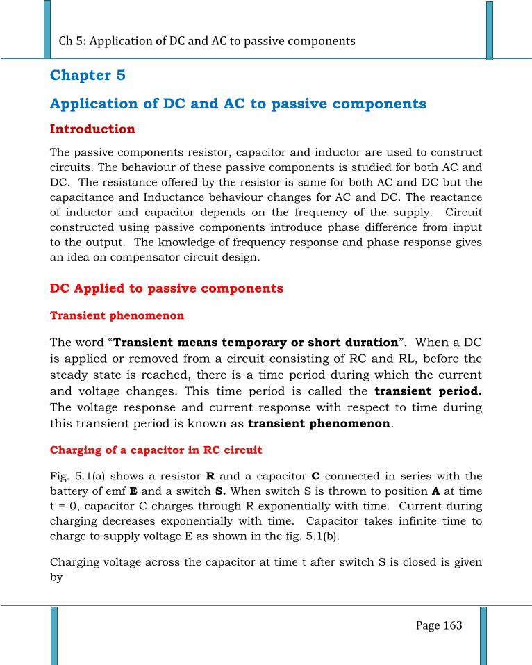
Ch 5: Application of DC and AC to passive components
Page 163
Chapter 5
Application of DC and AC to passive components
Introduction
The passive components resistor, capacitor and inductor are used to construct
circuits. The behaviour of these passive components is studied for both AC and
DC. The resistance offered by the resistor is same for both AC and DC but the
capacitance and Inductance behaviour changes for AC and DC. The reactance
of inductor and capacitor depends on the frequency of the supply. Circuit
constructed using passive components introduce phase difference from input
to the output. The knowledge of frequency response and phase response gives
an idea on compensator circuit design.
DC Applied to passive components
Transient phenomenon
The word “Transient means temporary or short duration”. When a DC
is applied or removed from a circuit consisting of RC and RL, before the
steady state is reached, there is a time period during which the current
and voltage changes. This time period is called the transient period.
The voltage response and current response with respect to time during
this transient period is known as transient phenomenon.
Charging of a capacitor in RC circuit
Fig. 5.1(a) shows a resistor R and a capacitor C connected in series with the
battery of emf E and a switch S. When switch S is thrown to position A at time
t = 0, capacitor C charges through R exponentially with time. Current during
charging decreases exponentially with time. Capacitor takes infinite time to
charge to supply voltage E as shown in the fig. 5.1(b).
Charging voltage across the capacitor at time t after switch S is closed is given
by
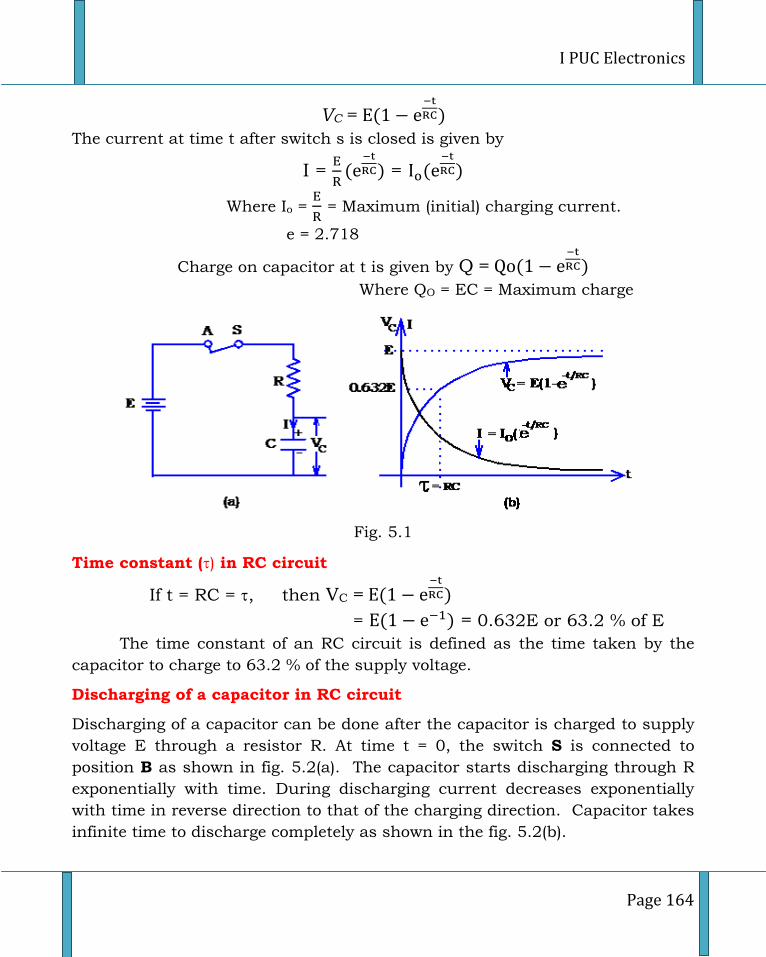
I PUC Electronics
Page 164
VC =
The current at time t after switch s is closed is given by
I =
=
Where Io =
= Maximum (initial) charging current.
e = 2.718
Charge on capacitor at t is given by Q =
Where QO = EC = Maximum charge
Fig. 5.1
Time constant () in RC circuit
If t = RC = , then VC =
= = 0.632E or 63.2 % of E
The time constant of an RC circuit is defined as the time taken by the
capacitor to charge to 63.2 % of the supply voltage.
Discharging of a capacitor in RC circuit
Discharging of a capacitor can be done after the capacitor is charged to supply
voltage E through a resistor R. At time t = 0, the switch S is connected to
position B as shown in fig. 5.2(a). The capacitor starts discharging through R
exponentially with time. During discharging current decreases exponentially
with time in reverse direction to that of the charging direction. Capacitor takes
infinite time to discharge completely as shown in the fig. 5.2(b).
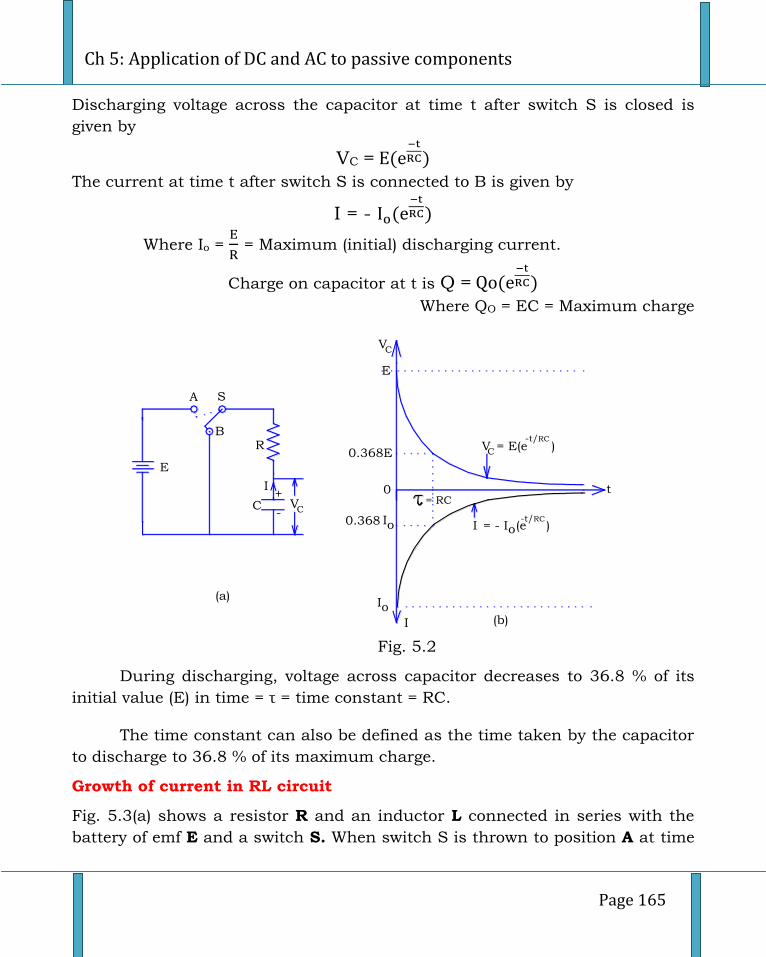
Ch 5: Application of DC and AC to passive components
Page 165
Discharging voltage across the capacitor at time t after switch S is closed is
given by
VC =
The current at time t after switch S is connected to B is given by
I = -
Where Io =
= Maximum (initial) discharging current.
Charge on capacitor at t is Q =
Where QO = EC = Maximum charge
R
VCC
E
+
-
I
SA
B
t
VC
E
I = - I (e )-t/RC
0.368E
= RC
V = E(e )C
-t/RC
I
0.368o
Io
Io
0
(a)
(b)
Fig. 5.2
During discharging, voltage across capacitor decreases to 36.8 % of its
initial value (E) in time = τ = time constant = RC.
The time constant can also be defined as the time taken by the capacitor
to discharge to 36.8 % of its maximum charge.
Growth of current in RL circuit
Fig. 5.3(a) shows a resistor R and an inductor L connected in series with the
battery of emf E and a switch S. When switch S is thrown to position A at time
I PUC Electronics
Page 166
t = 0, current grows exponentially with time as shown in fig 5.3(b). At t = 0, VL
is maximum and VR is zero. As the time increases, VL decreases exponentially
and VR increases exponentially.
The current I at time t after switch S is closed is given by
I= (
)
Where Io =
= Maximum current or current at t = ∞.
L
VRR
E+
-
SA
t
I = I (1-e )0.632
= RC
I
o
(a) (b)
VL
Io
Io
R
Lt-
I
Fig. 5.3
Time constant () in RL circuit
If t =
= , then I =
(
)
= = 0.632Io or 63.2 % of Io
The time constant of an RL circuit is defined as the time taken by the
current to grow 63.2 % of the maximum value.
Decay of the current in RL circuit
Decay of current in RL circuit takes place once the current in the inductor is
grown through a resistor R. In the fig. 5.4(a) initially the current in the circuit
is grown to maximum value using supply voltage E through a resistor R by
placing switch S to position A. At time t = 0, the switch S is connected to
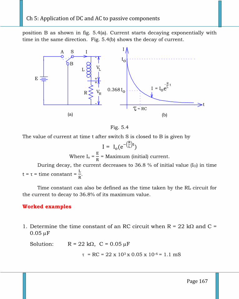
Ch 5: Application of DC and AC to passive components
Page 167
position B as shown in fig. 5.4(a). Current starts decaying exponentially with
time in the same direction. Fig. 5.4(b) shows the decay of current.
L
VRR
E+
-
SA
B
t
I = I e0.368
= RC
I
o
(a) (b)
VL
Io
Io
R
Lt-
I
+
-
Fig. 5.4
The value of current at time t after switch S is closed to B is given by
I = (
)
Where Io =
= Maximum (initial) current.
During decay, the current decreases to 36.8 % of initial value (IO) in time
t = τ = time constant =
.
Time constant can also be defined as the time taken by the RL circuit for
the current to decay to 36.8% of its maximum value.
Worked examples
1. Determine the time constant of an RC circuit when R = 22 k and C =
0.05 F
Solution: R = 22 k, C = 0.05 F
= RC = 22 x 103 x 0.05 x 10-6 = 1.1 mS
I PUC Electronics
Page 168
2. Determine the voltage across the capacitor and maximum current during charging at t = 1 S in a DC circuit containing R = 1 MΩ and C = 1 µF connected to DC supply of 10 V.
Solution: E = 10 V, R = 1 MΩ, C = 1 µF
RC = 1 x 106 x 1 x 10-6 = 1 S
VC=
= =10 x 0.632 = 6.32 V
Io =
=
= 10 µA
3. Determine the current through an inductor during the growth at
t = 1 S in a DC circuit containing R = 1 Ω and L = 1 H connected to DC supply of 20 V.
Solution: E = 20 V, R = 1 Ω, L = 1 H
Io =
=
= 20 A
I = (
)
I =
I = 12.64 = 12.64 A
4. Determine time constant and peak current of an RL circuit with DC source
of 10 V having a resistance R = 100 Ω and L = 100 mH.
Solution: E = 10 V, R = 100 , L = 100 mH
=
=
= 1 mS
Io =
=
= 100 mA
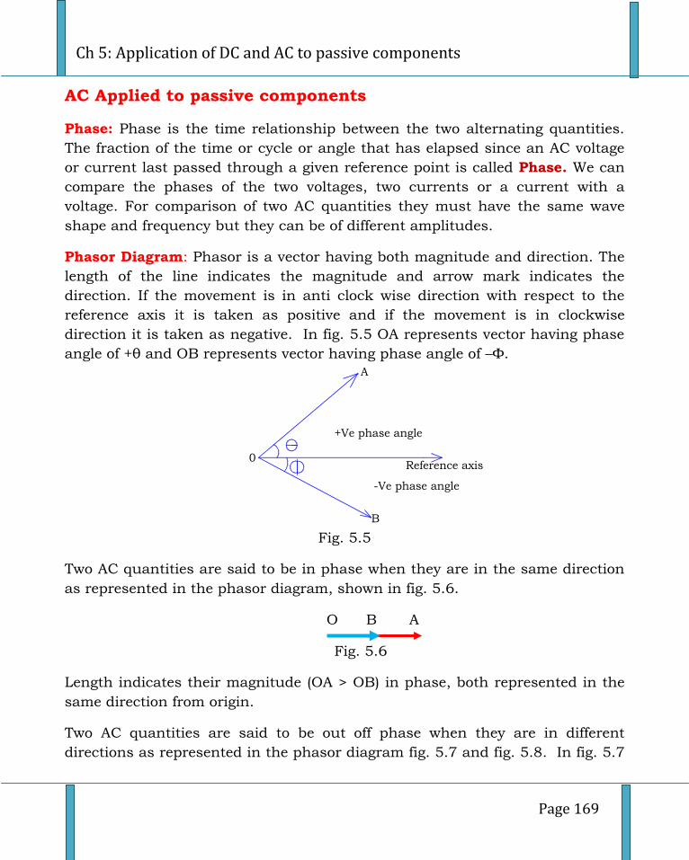
Ch 5: Application of DC and AC to passive components
Page 169
AC Applied to passive components
Phase: Phase is the time relationship between the two alternating quantities.
The fraction of the time or cycle or angle that has elapsed since an AC voltage
or current last passed through a given reference point is called Phase. We can
compare the phases of the two voltages, two currents or a current with a
voltage. For comparison of two AC quantities they must have the same wave
shape and frequency but they can be of different amplitudes.
Phasor Diagram: Phasor is a vector having both magnitude and direction. The
length of the line indicates the magnitude and arrow mark indicates the
direction. If the movement is in anti clock wise direction with respect to the
reference axis it is taken as positive and if the movement is in clockwise
direction it is taken as negative. In fig. 5.5 OA represents vector having phase
angle of +θ and OB represents vector having phase angle of –Φ.
Reference axis
+Ve phase angle
-Ve phase angle
0
A
B Fig. 5.5
Two AC quantities are said to be in phase when they are in the same direction
as represented in the phasor diagram, shown in fig. 5.6.
O B A
Fig. 5.6
Length indicates their magnitude (OA > OB) in phase, both represented in the
same direction from origin.
Two AC quantities are said to be out off phase when they are in different
directions as represented in the phasor diagram fig. 5.7 and fig. 5.8. In fig. 5.7
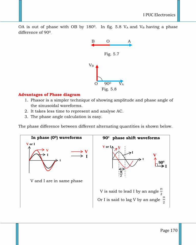
I PUC Electronics
Page 170
OA is out of phase with OB by 1800. In fig. 5.8 VA and VB having a phase
difference of 900.
B O A
Fig. 5.7
VB
O 900 VA
Fig. 5.8
Advantages of Phase diagram
1. Phasor is a simpler technique of showing amplitude and phase angle of
the sinusoidal waveforms.
2. It takes less time to represent and analyse AC.
3. The phase angle calculation is easy.
The phase difference between different alternating quantities is shown below.
In phase (00) waveforms
V and I are in same phase
90 phase shift waveforms
V is said to lead I by an angle
Or I is said to lag V by an angle
I
V or I
t
V
2
2
V
I
V or I
t
V I V
I 90
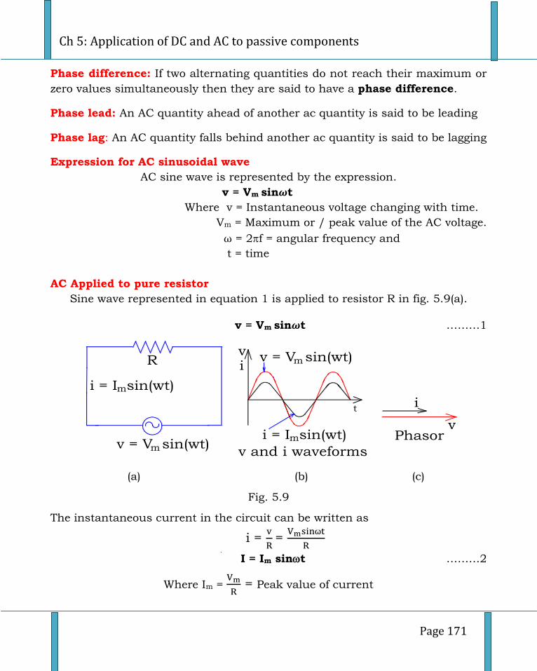
Ch 5: Application of DC and AC to passive components
Page 171
Phase difference: If two alternating quantities do not reach their maximum or
zero values simultaneously then they are said to have a phase difference.
Phase lead: An AC quantity ahead of another ac quantity is said to be leading
Phase lag: An AC quantity falls behind another ac quantity is said to be lagging
Expression for AC sinusoidal wave
AC sine wave is represented by the expression.
v = Vm sin t
Where v = Instantaneous voltage changing with time.
Vm = Maximum or / peak value of the AC voltage.
= 2f = angular frequency and
t = time
AC Applied to pure resistor
Sine wave represented in equation 1 is applied to resistor R in fig. 5.9(a).
v = Vm sin t ………1
i = I sin(wt)
R
v = V sin(wt)m
m
i
t
v v = V sin(wt)m
i = I sin(wt)m
v
i
Phasor
v and i waveforms
(a) (b) (c)
Fig. 5.9
The instantaneous current in the circuit can be written as
i =
=
I = Im sint ………2
Where Im =
= Peak value of current
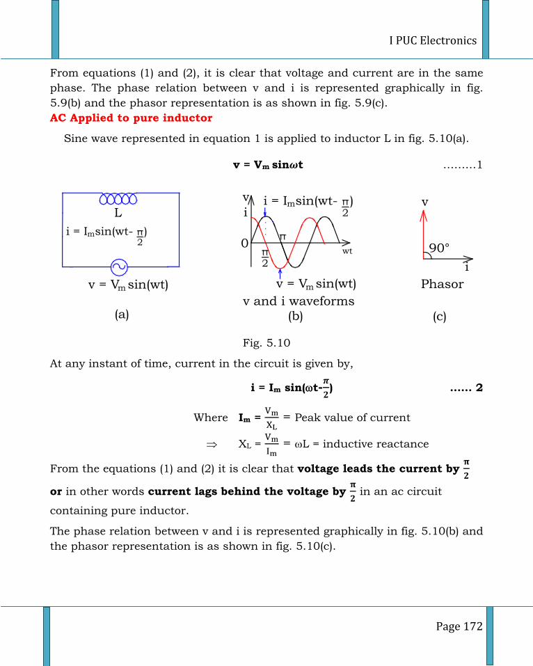
I PUC Electronics
Page 172
From equations (1) and (2), it is clear that voltage and current are in the same
phase. The phase relation between v and i is represented graphically in fig.
5.9(b) and the phasor representation is as shown in fig. 5.9(c).
AC Applied to pure inductor
Sine wave represented in equation 1 is applied to inductor L in fig. 5.10(a).
v = Vm sin t ………1
L
v = V sin(wt)m
i
wt
v
v = V sin(wt)m
i = I sin(wt- )m
i
Phasor
v and i waveforms
2
i = I sin(wt- )m2
v
90°2
0
(a) (b) (c)
Fig. 5.10
At any instant of time, current in the circuit is given by,
i = Im sin(t-
) …… 2
Where Im =
= Peak value of current
XL =
= L = inductive reactance
From the equations (1) and (2) it is clear that voltage leads the current by
or in other words current lags behind the voltage by
in an ac circuit
containing pure inductor.
The phase relation between v and i is represented graphically in fig. 5.10(b) and
the phasor representation is as shown in fig. 5.10(c).
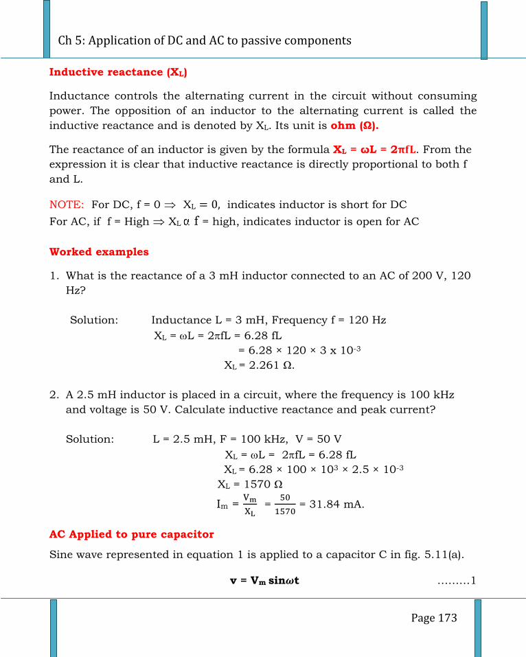
Ch 5: Application of DC and AC to passive components
Page 173
Inductive reactance (XL)
Inductance controls the alternating current in the circuit without consuming
power. The opposition of an inductor to the alternating current is called the
inductive reactance and is denoted by XL. Its unit is ohm (Ω).
The reactance of an inductor is given by the formula XL = ωL = 2 . From the
expression it is clear that inductive reactance is directly proportional to both f
and L.
NOTE: For DC, f = 0 XL indicates inductor is short for DC
For AC, if f = High XL f = high, indicates inductor is open for AC
Worked examples
1. What is the reactance of a 3 mH inductor connected to an AC of 200 V, 120
Hz?
Solution: Inductance L = 3 mH, Frequency f = 120 Hz
XL = L = 2fL = 6.28 fL
= 6.28 × 120 × 3 x 10-3
XL = 2.261 Ω.
2. A 2.5 mH inductor is placed in a circuit, where the frequency is 100 kHz
and voltage is 50 V. Calculate inductive reactance and peak current?
Solution: L = 2.5 mH, F = 100 kHz, V = 50 V
XL = L = 2fL = 6.28 fL
XL = 6.28 × 100 × 103 × 2.5 × 10-3
XL = 1570 Ω
Im =
=
= 31.84 mA.
AC Applied to pure capacitor
Sine wave represented in equation 1 is applied to a capacitor C in fig. 5.11(a).
v = Vm sin t ………1
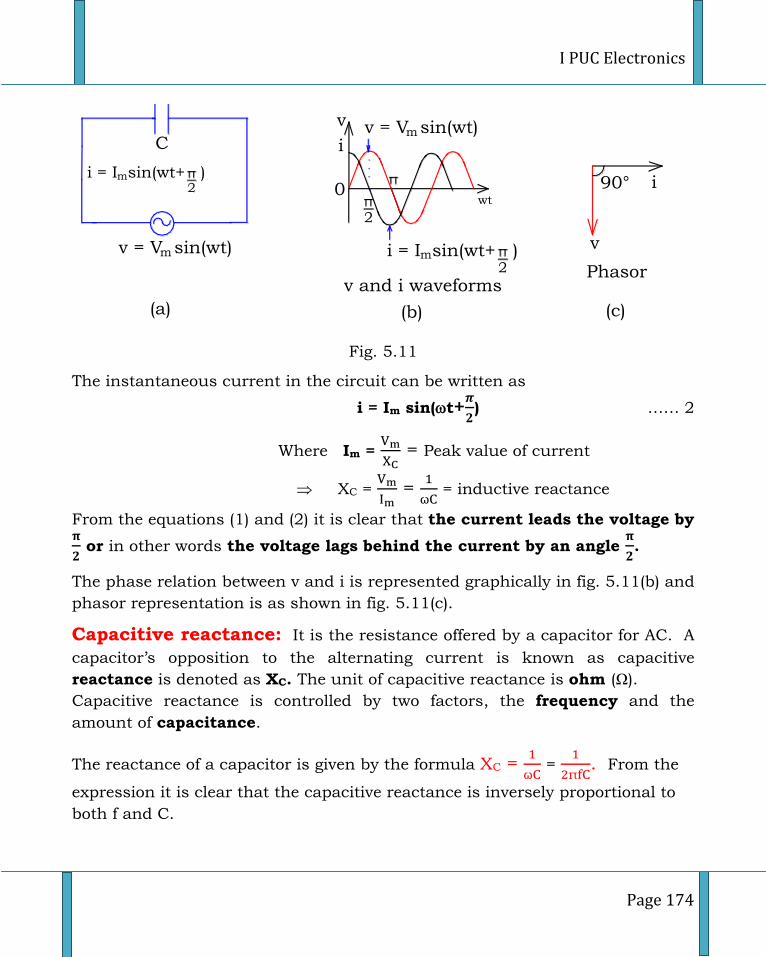
I PUC Electronics
Page 174
v = V sin(wt)m
i
wt
v v = V sin(wt)m
i = I sin(wt+ )m
i
Phasorv and i waveforms
2
i = I sin(wt+ )m2
v
90°
2
0
(a) (b) (c)
C
Fig. 5.11
The instantaneous current in the circuit can be written as
i = Im sin(t+
) …… 2
Where Im =
= Peak value of current
XC =
=
= inductive reactance
From the equations (1) and (2) it is clear that the current leads the voltage by
or in other words the voltage lags behind the current by an angle
.
The phase relation between v and i is represented graphically in fig. 5.11(b) and
phasor representation is as shown in fig. 5.11(c).
Capacitive reactance: It is the resistance offered by a capacitor for AC. A
capacitor’s opposition to the alternating current is known as capacitive
reactance is denoted as XC. The unit of capacitive reactance is ohm (Ω).
Capacitive reactance is controlled by two factors, the frequency and the
amount of capacitance.
The reactance of a capacitor is given by the formula XC =
=
. From the
expression it is clear that the capacitive reactance is inversely proportional to
both f and C.
Ch 5: Application of DC and AC to passive components
Page 175
NOTE: For DC, f = 0 XC =
indicates capacitor is open for DC
For AC, if f = High XC
= low, indicates capacitor is short for AC
Worked example
1. What is the capacitive reactance of a 0.01 µF capacitor at 400 Hz?
Solutions: Given C = 0.01 µF, f = 400 Hz
XC =
=
=
XC = 39800 Ω = 39.8 kΩ
Power in AC Circuits
Power is the important quantity in all electronic circuits and the
communication systems. These involve transmission of power from one point to
another. The instantaneous power delivered or absorbed by an element in AC
circuits is given by p = v i, where v and i are instantaneous values of AC
voltage and current respectively.
The instantaneous power changes with time and it is difficult to measure,
therefore it is convenient to measure the average power delivered.
Average Power
The average of the instantaneous power over one cycle is called average power
(Pav). The average power consumed in an ac circuit is also known as active
power (Pact). It is measured in watt.
Therefore
Average power = Active power = Pav = Pact = Vrms IrmscosΦ
Where Vrms =
√ and Irms =
√
Where Φ is the phase difference between the applied voltage and the resulting
current.
Case 1: In a resistive circuit, current and voltage are in phase i.e., Φ is 00, the
average power dissipated in a resistor is given by
Pav = Vrms Irms, (cosΦ = cos00 = 1)
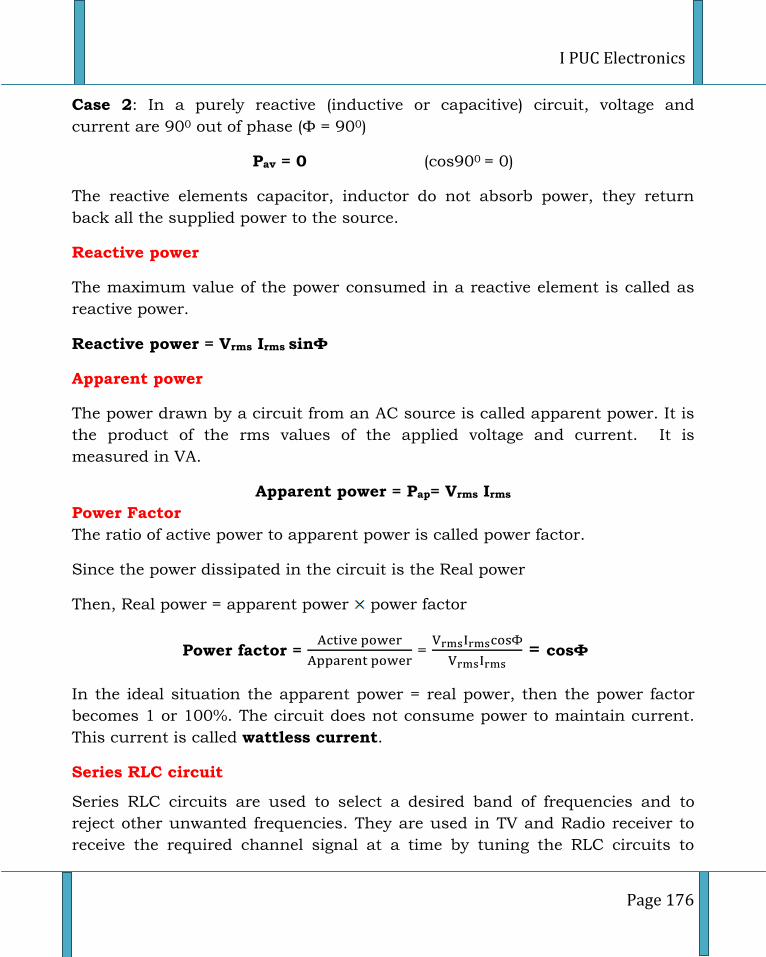
I PUC Electronics
Page 176
Case 2: In a purely reactive (inductive or capacitive) circuit, voltage and
current are 900 out of phase (Φ = 900)
Pav = 0 (cos900 = 0)
The reactive elements capacitor, inductor do not absorb power, they return
back all the supplied power to the source.
Reactive power
The maximum value of the power consumed in a reactive element is called as
reactive power.
Reactive power = Vrms Irms sinΦ
Apparent power
The power drawn by a circuit from an AC source is called apparent power. It is
the product of the rms values of the applied voltage and current. It is
measured in VA.
Apparent power = Pap= Vrms Irms
Power Factor
The ratio of active power to apparent power is called power factor.
Since the power dissipated in the circuit is the Real power
Then, Real power = apparent power power factor
Power factor =
=
Φ
= cosΦ
In the ideal situation the apparent power = real power, then the power factor
becomes 1 or 100%. The circuit does not consume power to maintain current.
This current is called wattless current.
Series RLC circuit
Series RLC circuits are used to select a desired band of frequencies and to
reject other unwanted frequencies. They are used in TV and Radio receiver to
receive the required channel signal at a time by tuning the RLC circuits to
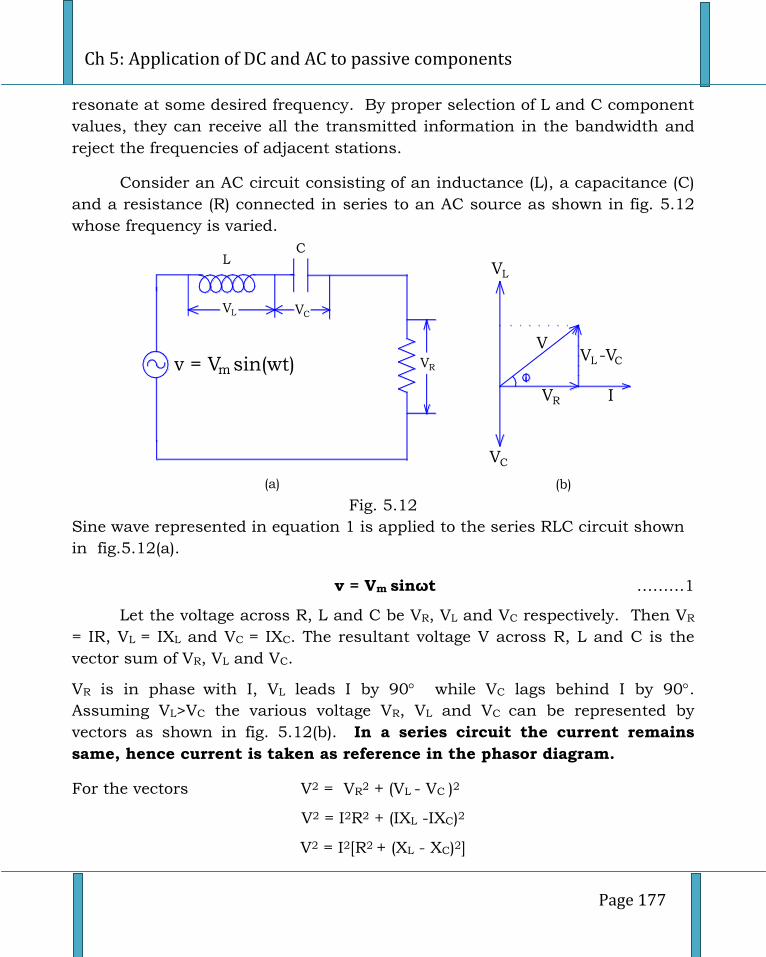
Ch 5: Application of DC and AC to passive components
Page 177
resonate at some desired frequency. By proper selection of L and C component
values, they can receive all the transmitted information in the bandwidth and
reject the frequencies of adjacent stations.
Consider an AC circuit consisting of an inductance (L), a capacitance (C)
and a resistance (R) connected in series to an AC source as shown in fig. 5.12
whose frequency is varied.
LC
VL VC
VRv = V sin(wt)m
VC
VL -V C
VR I
V
VL
(a) (b) Fig. 5.12
Sine wave represented in equation 1 is applied to the series RLC circuit shown
in fig.5.12(a).
v = Vm sinωt ………1
Let the voltage across R, L and C be VR, VL and VC respectively. Then VR
= IR, VL = IXL and VC = IXC. The resultant voltage V across R, L and C is the
vector sum of VR, VL and VC.
VR is in phase with I, VL leads I by 90 while VC lags behind I by 90.
Assuming VL>VC the various voltage VR, VL and VC can be represented by
vectors as shown in fig. 5.12(b). In a series circuit the current remains
same, hence current is taken as reference in the phasor diagram.
For the vectors V2 = VR2 + (VL
- VC )2
V2 = I2R2 + (IXL -IXC)2
V2 = I2[R2 + (XL - XC)2]
I PUC Electronics
Page 178
The impedance (Z) of the RLC circuit is therefore,
Z =
= √ ………2
The phase angle between the current and voltage in series RLC circuit is given
by
Φ = (
) ………3
Impedance Impedance of the series RLC circuit is total opposition offered by R, L and C to
AC. Fig. 5.13 shows the variation of impedance with frequency. At resonant
frequency fr inductive reactance XL = XC. Below fr, XL<XC and above fr, XL>XC.
f
Z
Z = R
X =L XC
X <L XC X >L X
C
fr
Fig. 5.13
Note:
If XL > XC, is positive, the current lags the voltage by an angle and the
circuit is inductive in nature.
If XL< XC, is negative, the current leads the voltage by an angle and
the circuit is capacitive in nature.
If XL = XC, then the circuit is said to be in resonance. The voltage and
current are in phase ( = 0) and the impedance Z is purely resistive.
Condition for resonance
At resonance inductive reactance XL is equal to capacitive reactance XC.
The frequency at resonance is called the resonant frequency fr.
At resonance, XL = XC
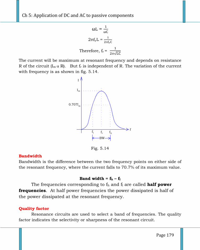
Ch 5: Application of DC and AC to passive components
Page 179
L =
2 L =
Therefore, fr =
√
The current will be maximum at resonant frequency and depends on resistance
R of the circuit (Im . But fr is independent of R. The variation of the current
with frequency is as shown in fig. 5.14.
f
I
fr
Im
0.707Im
fl fh
BW
Fig. 5.14
Bandwidth
Bandwidth is the difference between the two frequency points on either side of
the resonant frequency, where the current falls to 70.7% of its maximum value.
Band width = fh – fl
The frequencies corresponding to fh and fl are called half power
frequencies. At half power frequencies the power dissipated is half of
the power dissipated at the resonant frequency.
Quality factor
Resonance circuits are used to select a band of frequencies. The quality
factor indicates the selectivity or sharpness of the resonant circuit.
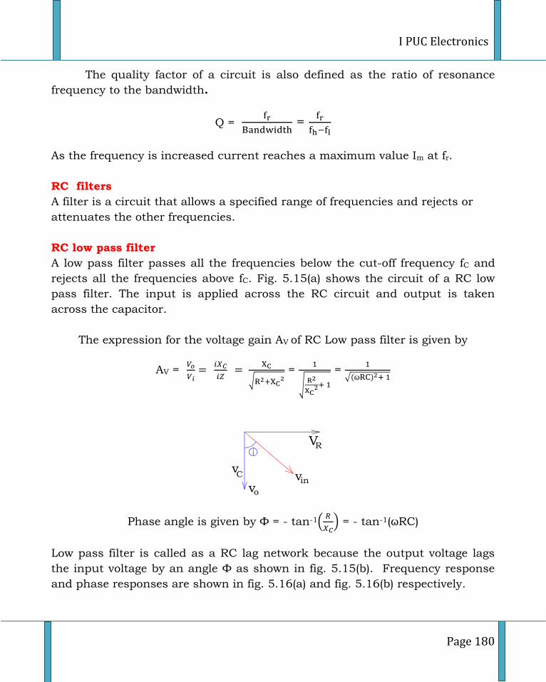
I PUC Electronics
Page 180
The quality factor of a circuit is also defined as the ratio of resonance
frequency to the bandwidth.
Q =
=
As the frequency is increased current reaches a maximum value Im at fr.
RC filters
A filter is a circuit that allows a specified range of frequencies and rejects or
attenuates the other frequencies.
RC low pass filter
A low pass filter passes all the frequencies below the cut-off frequency fC and
rejects all the frequencies above fC. Fig. 5.15(a) shows the circuit of a RC low
pass filter. The input is applied across the RC circuit and output is taken
across the capacitor.
The expression for the voltage gain AV of RC Low pass filter is given by
AV =
√ =
√
=
√
VR
vinvo
Cv
Phase angle is given by Φ = - tan-1(
) = - tan-1( RC)
Low pass filter is called as a RC lag network because the output voltage lags
the input voltage by an angle Φ as shown in fig. 5.15(b). Frequency response
and phase responses are shown in fig. 5.16(a) and fig. 5.16(b) respectively.
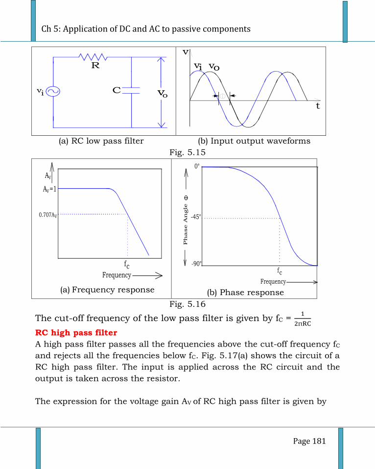
Ch 5: Application of DC and AC to passive components
Page 181
R
Cvi vo
v
t
i vo
(a) RC low pass filter (b) Input output waveforms
Fig. 5.15
A =1
0.707A
Frequency
fc
V
V
AV
(a) Frequency response
-90°
-45°
Ph
ase A
ngle
Frequency
0°
fc
(b) Phase response
Fig. 5.16
The cut-off frequency of the low pass filter is given by fC =
RC high pass filter
A high pass filter passes all the frequencies above the cut-off frequency fC
and rejects all the frequencies below fC. Fig. 5.17(a) shows the circuit of a
RC high pass filter. The input is applied across the RC circuit and the
output is taken across the resistor.
The expression for the voltage gain AV of RC high pass filter is given by
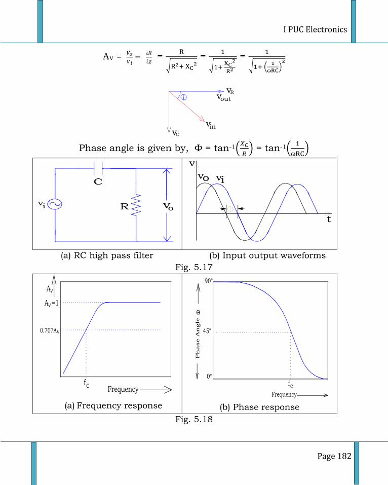
I PUC Electronics
Page 182
AV =
=
√ =
√
=
√ (
)
vinvC
voutR
Phase angle is given by, Φ = tan-1(
) = tan-1(
)
C
vi voR
v
t
ivo
(a) RC high pass filter (b) Input output waveforms
Fig. 5.17
A =1
0.707A
Frequencyfc
V
V
AV
(a) Frequency response
0°
45°
Ph
ase A
ngle
Frequency
90°
fc
(b) Phase response
Fig. 5.18
Ch 5: Application of DC and AC to passive components
Page 183
High pass filter is called as a RC lead network because the output voltage
leads the input voltage by an angle Φ as shown in fig. 5.17(b).
Frequency response and phase responses are shown in fig. 5.18(a)
and fig. 5.18(b) respectively.
The cut-off frequency of the high pass filter is given by fC =
Worked examples:
1. A 10 Ω resistance in series with XL = 50 Ω and XC = 25 Ω. The applied
voltage is V = 50 mV with 50 Hz. Calculate Z, I and phase angle.
XL - XC = 50 – 25 = 25 Ω.
Z = √ = 26.92 Ω.
I =
=
= 1. 85 mA
= (
) = (
) = 68.190
2. An inductor of 20 mH is connected in series with a resistor of 50 Ω. The
combination is connected to 220 V, 50 Hz source. Find the current in the
circuit.
Solution: Given L = 20 mH, R = 50 Ω, V = 220 V, f = 50 Hz.
The current, I =
Z = √ = √ = 50. 39 Ω
I =
= 4.36 A
3. A series RL circuit is connected across the ac supply of 150 V, 60 Hz. Find
the phase angle if R = 10 Ω and L = 40 mH.
Solution: Given R = 10 Ω, L = 40 mH, V = 150 V, f = 60 Hz.
I PUC Electronics
Page 184
Φ = (
) = (
) = (
)
= (
) = 56.430
4. A series RLC circuit has R = 20 Ω, C = 0.01 µF, L = 10 mH. Calculate (a)
Resonent frequency.
Solution: Given R = 20 Ω, C = 0.01 µF, L = 10 mH
Resonant frequency, fr =
√ =
√ = 15.9 kHz
Exercise
1. Determine time constant of an RC circuit when resistor is 20 k and
Capacitor is 0.05 F (Ans: = 1 mS)
2. The time constant of an RL circuit is 4 mS. if L = 100 mH, calculate the
value of resistance. (Ans: R = 25 )
3. What value of resistance must be connected in series with a 20 F.
capacitor to provide a time constant of 0.2 sec? (Ans: R = 10 k)
4. A coil of 100 mH having a resistance of 100 Ω is connected across a source
of 200 V, 50 Hz. Find the phase angle and current in the circuit.
(Ans: Φ = 17.430, I = 1.9 A)
5. A series resonant circuit has R = 100 Ω, C = 0.1 µF produces a resonant
frequency of 3 kHz. Find the value of inductance. (Ans: L = 28.17 mH)
One mark questions
1. What is transient period?
2. What is transient phenomenon?
3. Define time constant of RC circuit.
4. Write an expression for the voltage across capacitor during charging.
5. Write an expression for instantaneous current in R-L circuit, during
the growth of current.
6. Write an expression for instantaneous current in R-L circuit, during
the decay of current.
Ch 5: Application of DC and AC to passive components
Page 185
7. Define the time constant of RL circuit.
8. Define the phase difference between two AC quantities.
9. Two AC quantities are in phase. What is the value of phase angle
between them?
10. Draw the waveform of two in phase AC quantities.
11. Draw the waveform of two AC quantities that are 1800 out of phase.
12. What is a phasor diagram?
13. Write the phasor diagram of two AC quantities that are 900 out of
phase.
14. What is the phase difference between voltage and current in a purely
resistive circuit?
15. Draw the phasor diagram of voltage and current in a purely
capacitive circuit?
16. What is capacitive reactance?.
17. Give the unit of capacitive reactance.
18. Write the expression for the capacitive reactance.
19. Define average power.
20. Define power factor.
21. Define impedance.
22. What is the unit of impedance?
23. Write the expression for the impedance of a series RLC circuit.
24. Give the condition for resonance of a series RLC circuit.
25. Write the expression for the resonance frequency of a series
resonance circuit.
26. What are half power frequencies?
27. Define quality factor.
28. Write the relation between quality factor, bandwidth and resonance
frequency.
29. What is a low pass filter?
30. What is a high pass filter?
I PUC Electronics
Page 186
Two marks question
1. Draw the graph showing voltage across capacitor during charging.
2. Draw the graph of growth of current in RL circuit.
3. Define capacitive reactance and give the expression for the capacitive
reactance.
4. Define Inductive reactance and give the expression for the inductive
reactance.
5. Write a brief note on impedance of a circuit.
6. Write a note on the variation of impedance in a series RLC circuit
with frequency.
7. Derive an expression for resonance frequency of a series resonance
circuit.
8. Draw the circuit diagram of low pass filter and high pass filter.
Three/five marks question
1. Discuss the charging of capacitor in a RC circuit.
2. Discuss the discharging of capacitor in a RC circuit.
3. Discuss the growth of current in a RL circuit.
4. Discuss the decay of current in a RL circuit.
5. Describe the phenomenon of resonance in a series resonant circuit.
6. Derive an expression for resonant frequency of a series resonant
circuit.
7. Explain low pass filter with its frequency response.
8. Explain high pass filter with its phase response.
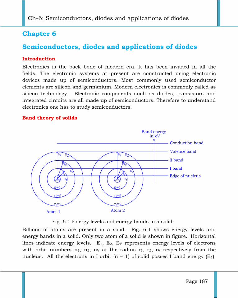
Ch-6: Semiconductors, diodes and applications of diodes
Page 187
Chapter 6
Semiconductors, diodes and applications of diodes
Introduction
Electronics is the back bone of modern era. It has been invaded in all the
fields. The electronic systems at present are constructed using electronic
devices made up of semiconductors. Most commonly used semiconductor
elements are silicon and germanium. Modern electronics is commonly called as
silicon technology. Electronic components such as diodes, transistors and
integrated circuits are all made up of semiconductors. Therefore to understand
electronics one has to study semiconductors.
Band theory of solids
r
Core
V
r2
r1
n=1
n=2
n=V
Ev
E2
E1
r
Core
V
r2
r1
n=1
n=2
n=V
Ev
E2
E1
Valence band
Conduction band
I band
II band
Edge of nucleus
in eVBand energy
Atom 1 Atom 2
Fig. 6.1 Energy levels and energy bands in a solid
Billions of atoms are present in a solid. Fig. 6.1 shows energy levels and
energy bands in a solid. Only two atom of a solid is shown in figure. Horizontal
lines indicate energy levels. E1, E2, EV represents energy levels of electrons
with orbit numbers n1, n2, nV at the radius r1, r2, rV respectively from the
nucleus. All the electrons in I orbit (n = 1) of solid posses I band energy (E1),
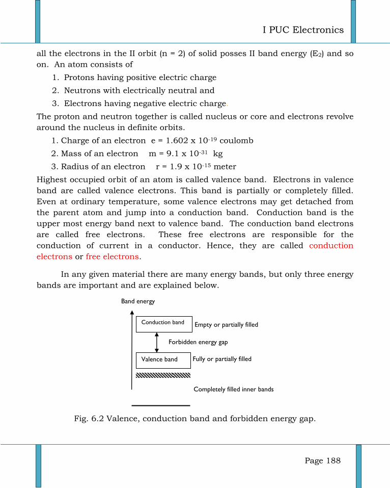
I PUC Electronics
Page 188
all the electrons in the II orbit (n = 2) of solid posses II band energy (E2) and so
on. An atom consists of
1. Protons having positive electric charge
2. Neutrons with electrically neutral and
3. Electrons having negative electric charge.
The proton and neutron together is called nucleus or core and electrons revolve
around the nucleus in definite orbits.
1. Charge of an electron e = 1.602 x 10⁻¹⁹ coulomb
2. Mass of an electron m = 9.1 x 10⁻³¹ kg
3. Radius of an electron r = 1.9 x 10⁻¹⁵ meter
Highest occupied orbit of an atom is called valence band. Electrons in valence
band are called valence electrons. This band is partially or completely filled.
Even at ordinary temperature, some valence electrons may get detached from
the parent atom and jump into a conduction band. Conduction band is the
upper most energy band next to valence band. The conduction band electrons
are called free electrons. These free electrons are responsible for the
conduction of current in a conductor. Hence, they are called conduction
electrons or free electrons.
In any given material there are many energy bands, but only three energy
bands are important and are explained below.
Fig. 6.2 Valence, conduction band and forbidden energy gap.
Band energy
Completely filled inner bands
Conduction band
Valence band
Empty or partially filled
Forbidden energy gap
filled Conduction band
Fully or partially filled
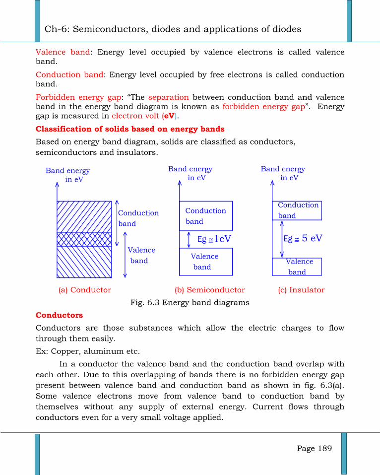
Ch-6: Semiconductors, diodes and applications of diodes
Page 189
Valence band: Energy level occupied by valence electrons is called valence band.
Conduction band: Energy level occupied by free electrons is called conduction band.
Forbidden energy gap: “The separation between conduction band and valence band in the energy band diagram is known as forbidden energy gap”. Energy gap is measured in electron volt (eV).
Classification of solids based on energy bands
Based on energy band diagram, solids are classified as conductors,
semiconductors and insulators.
in eV
Band energy
Conduction
band
Valence
band
Conduction
band
Valence
bandValence
band
Conduction
band
in eV
Band energy
in eV
Band energy
Eg ~1eV Eg ~ 5 eV
(a) Conductor (b) Semiconductor (c) Insulator
Fig. 6.3 Energy band diagrams
Conductors
Conductors are those substances which allow the electric charges to flow
through them easily.
Ex: Copper, aluminum etc.
In a conductor the valence band and the conduction band overlap with
each other. Due to this overlapping of bands there is no forbidden energy gap
present between valence band and conduction band as shown in fig. 6.3(a).
Some valence electrons move from valence band to conduction band by
themselves without any supply of external energy. Current flows through
conductors even for a very small voltage applied.
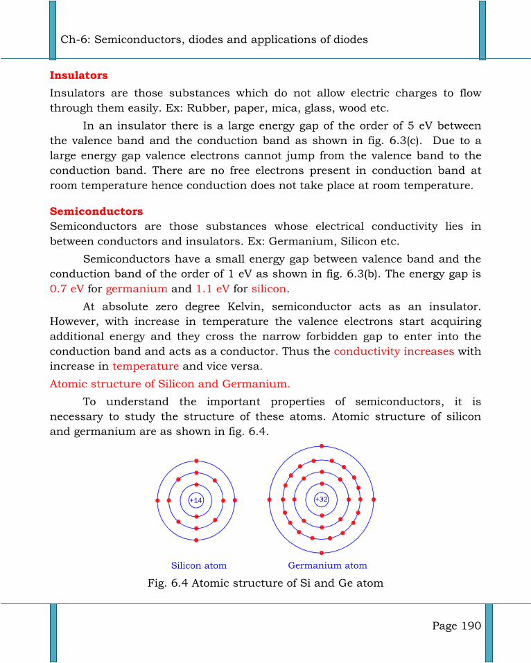
Ch-6: Semiconductors, diodes and applications of diodes
Page 190
Insulators
Insulators are those substances which do not allow electric charges to flow
through them easily. Ex: Rubber, paper, mica, glass, wood etc.
In an insulator there is a large energy gap of the order of 5 eV between
the valence band and the conduction band as shown in fig. 6.3(c). Due to a
large energy gap valence electrons cannot jump from the valence band to the
conduction band. There are no free electrons present in conduction band at
room temperature hence conduction does not take place at room temperature.
Semiconductors
Semiconductors are those substances whose electrical conductivity lies in
between conductors and insulators. Ex: Germanium, Silicon etc.
Semiconductors have a small energy gap between valence band and the
conduction band of the order of 1 eV as shown in fig. 6.3(b). The energy gap is
0.7 eV for germanium and 1.1 eV for silicon.
At absolute zero degree Kelvin, semiconductor acts as an insulator.
However, with increase in temperature the valence electrons start acquiring
additional energy and they cross the narrow forbidden gap to enter into the
conduction band and acts as a conductor. Thus the conductivity increases with
increase in temperature and vice versa.
Atomic structure of Silicon and Germanium.
To understand the important properties of semiconductors, it is
necessary to study the structure of these atoms. Atomic structure of silicon
and germanium are as shown in fig. 6.4.
Germanium atom
+14 +32
Silicon atom
Fig. 6.4 Atomic structure of Si and Ge atom
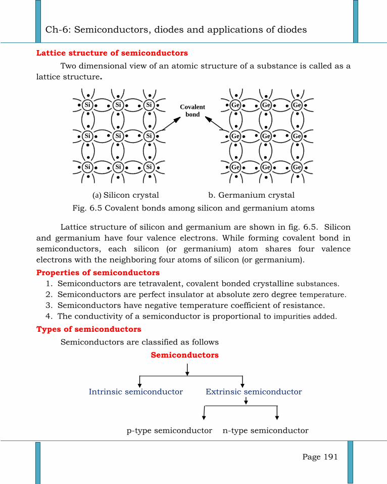
Ch-6: Semiconductors, diodes and applications of diodes
Page 191
Lattice structure of semiconductors
Two dimensional view of an atomic structure of a substance is called as a
lattice structure.
Ge
Ge
Ge Ge
Ge
Ge Ge
Ge
Ge
SiSi
Si Si Si
Si
SiSiSi
Covalent
bond
(a) Silicon crystal b. Germanium crystal
Fig. 6.5 Covalent bonds among silicon and germanium atoms
Lattice structure of silicon and germanium are shown in fig. 6.5. Silicon
and germanium have four valence electrons. While forming covalent bond in
semiconductors, each silicon (or germanium) atom shares four valence
electrons with the neighboring four atoms of silicon (or germanium).
Properties of semiconductors
1. Semiconductors are tetravalent, covalent bonded crystalline substances.
2. Semiconductors are perfect insulator at absolute zero degree temperature.
3. Semiconductors have negative temperature coefficient of resistance.
4. The conductivity of a semiconductor is proportional to impurities added.
Types of semiconductors
Semiconductors are classified as follows
Semiconductors
Intrinsic semiconductor Extrinsic semiconductor
p-type semiconductor n-type semiconductor
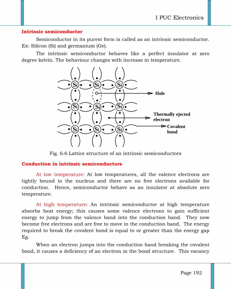
I PUC Electronics
Page 192
Intrinsic semiconductor
Semiconductor in its purest form is called as an intrinsic semiconductor.
Ex: Silicon (Si) and germanium (Ge).
The intrinsic semiconductor behaves like a perfect insulator at zero
degree kelvin. The behaviour changes with increase in temperature.
Si Si Si
Si Si Si
Si Si Si
Thermally ejected electron
Covalent bond
Hole
Fig. 6.6 Lattice structure of an intrinsic semiconductors
Conduction in intrinsic semiconductors
At low temperature: At low temperatures, all the valence electrons are
tightly bound to the nucleus and there are no free electrons available for
conduction. Hence, semiconductor behave as an insulator at absolute zero
temperature.
At high temperature: An intrinsic semiconductor at high temperature
absorbs heat energy; this causes some valence electrons to gain sufficient
energy to jump from the valence band into the conduction band. They now
become free electrons and are free to move in the conduction band. The energy
required to break the covalent bond is equal to or greater than the energy gap
Eg.
When an electron jumps into the conduction band breaking the covalent
bond, it causes a deficiency of an electron in the bond structure. This vacancy
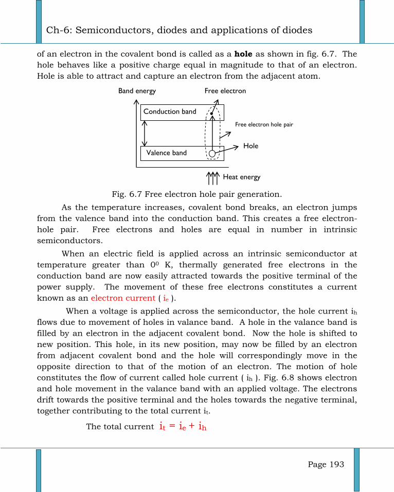
Ch-6: Semiconductors, diodes and applications of diodes
Page 193
of an electron in the covalent bond is called as a hole as shown in fig. 6.7. The
hole behaves like a positive charge equal in magnitude to that of an electron.
Hole is able to attract and capture an electron from the adjacent atom.
Fig. 6.7 Free electron hole pair generation.
As the temperature increases, covalent bond breaks, an electron jumps
from the valence band into the conduction band. This creates a free electron-
hole pair. Free electrons and holes are equal in number in intrinsic
semiconductors.
When an electric field is applied across an intrinsic semiconductor at
temperature greater than 00 K, thermally generated free electrons in the
conduction band are now easily attracted towards the positive terminal of the
power supply. The movement of these free electrons constitutes a current
known as an electron current ( ie ).
When a voltage is applied across the semiconductor, the hole current ih
flows due to movement of holes in valance band. A hole in the valance band is
filled by an electron in the adjacent covalent bond. Now the hole is shifted to
new position. This hole, in its new position, may now be filled by an electron
from adjacent covalent bond and the hole will correspondingly move in the
opposite direction to that of the motion of an electron. The motion of hole
constitutes the flow of current called hole current ( ih ). Fig. 6.8 shows electron
and hole movement in the valance band with an applied voltage. The electrons
drift towards the positive terminal and the holes towards the negative terminal,
together contributing to the total current it.
The total current it = ie + ih
Band energy
Conduction band
Valence band
Free electron
Free electron hole pair
Hole
Heat energy
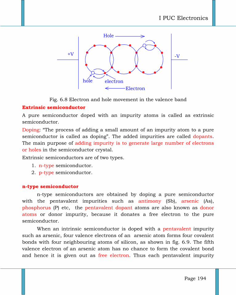
I PUC Electronics
Page 194
Electron
+V -V
hole electron
Hole
Fig. 6.8 Electron and hole movement in the valence band
Extrinsic semiconductor
A pure semiconductor doped with an impurity atoms is called as extrinsic
semiconductor.
Doping: “The process of adding a small amount of an impurity atom to a pure
semiconductor is called as doping”. The added impurities are called dopants.
The main purpose of adding impurity is to generate large number of electrons
or holes in the semiconductor crystal.
Extrinsic semiconductors are of two types.
1. n-type semiconductor.
2. p-type semiconductor.
n-type semiconductor
n-type semiconductors are obtained by doping a pure semiconductor
with the pentavalent impurities such as antimony (Sb), arsenic (As),
phosphorus (P) etc, the pentavalent dopant atoms are also known as donor
atoms or donor impurity, because it donates a free electron to the pure
semiconductor.
When an intrinsic semiconductor is doped with a pentavalent impurity
such as arsenic, four valence electrons of an arsenic atom forms four covalent
bonds with four neighbouring atoms of silicon, as shown in fig. 6.9. The fifth
valence electron of an arsenic atom has no chance to form the covalent bond
and hence it is given out as free electron. Thus each pentavalent impurity
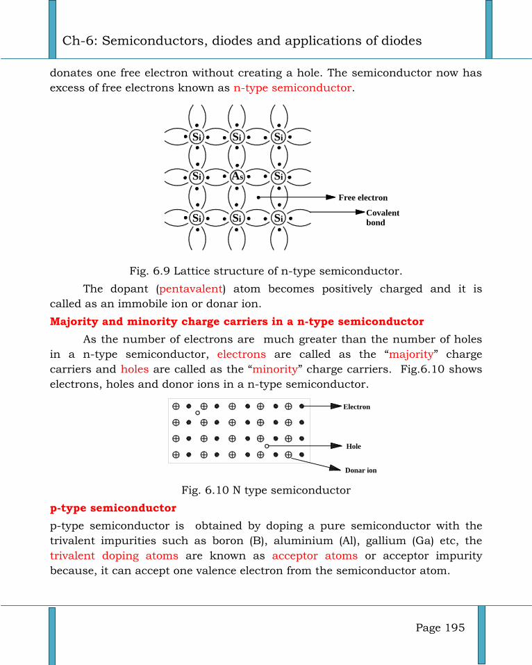
Ch-6: Semiconductors, diodes and applications of diodes
Page 195
donates one free electron without creating a hole. The semiconductor now has
excess of free electrons known as n-type semiconductor.
Si Si Si
Si As Si
Si Si Si
Free electron
Covalent bond
Fig. 6.9 Lattice structure of n-type semiconductor.
The dopant (pentavalent) atom becomes positively charged and it is
called as an immobile ion or donar ion.
Majority and minority charge carriers in a n-type semiconductor
As the number of electrons are much greater than the number of holes
in a n-type semiconductor, electrons are called as the “majority” charge
carriers and holes are called as the “minority” charge carriers. Fig.6.10 shows
electrons, holes and donor ions in a n-type semiconductor.
Electron
Hole
Donar ion
Fig. 6.10 N type semiconductor
p-type semiconductor
p-type semiconductor is obtained by doping a pure semiconductor with the
trivalent impurities such as boron (B), aluminium (Al), gallium (Ga) etc, the
trivalent doping atoms are known as acceptor atoms or acceptor impurity
because, it can accept one valence electron from the semiconductor atom.
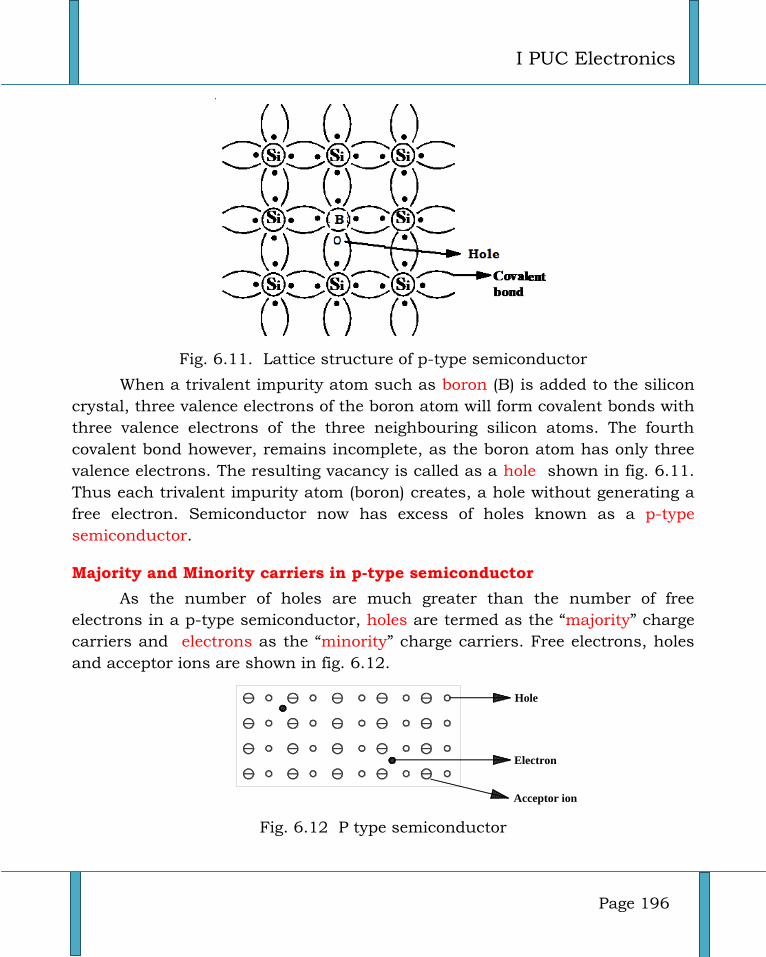
I PUC Electronics
Page 196
Fig. 6.11. Lattice structure of p-type semiconductor
When a trivalent impurity atom such as boron (B) is added to the silicon
crystal, three valence electrons of the boron atom will form covalent bonds with
three valence electrons of the three neighbouring silicon atoms. The fourth
covalent bond however, remains incomplete, as the boron atom has only three
valence electrons. The resulting vacancy is called as a hole shown in fig. 6.11.
Thus each trivalent impurity atom (boron) creates, a hole without generating a
free electron. Semiconductor now has excess of holes known as a p-type
semiconductor.
Majority and Minority carriers in p-type semiconductor
As the number of holes are much greater than the number of free
electrons in a p-type semiconductor, holes are termed as the “majority” charge
carriers and electrons as the “minority” charge carriers. Free electrons, holes
and acceptor ions are shown in fig. 6.12.
Hole
Electron
Acceptor ion
Fig. 6.12 P type semiconductor
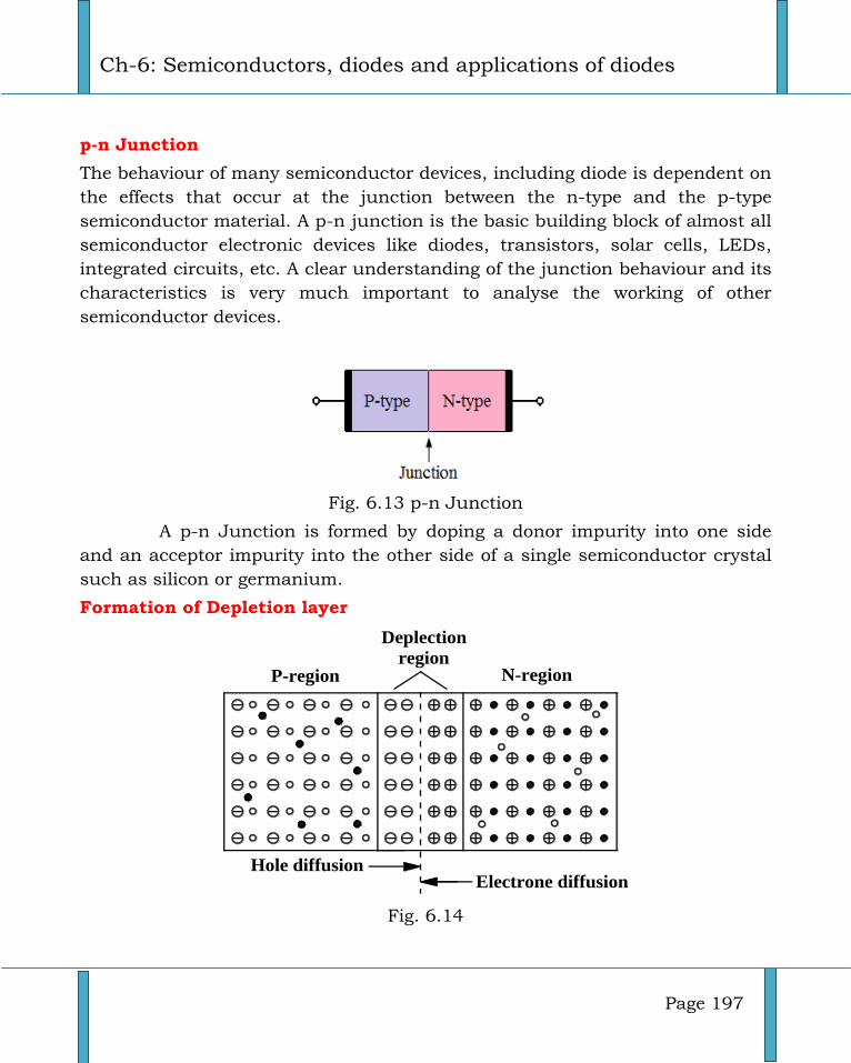
Ch-6: Semiconductors, diodes and applications of diodes
Page 197
p-n Junction
The behaviour of many semiconductor devices, including diode is dependent on
the effects that occur at the junction between the n-type and the p-type
semiconductor material. A p-n junction is the basic building block of almost all
semiconductor electronic devices like diodes, transistors, solar cells, LEDs,
integrated circuits, etc. A clear understanding of the junction behaviour and its
characteristics is very much important to analyse the working of other
semiconductor devices.
Fig. 6.13 p-n Junction
A p-n Junction is formed by doping a donor impurity into one side
and an acceptor impurity into the other side of a single semiconductor crystal
such as silicon or germanium.
Formation of Depletion layer
Deplection
regionN-regionP-region
Hole diffusionElectrone diffusion
Fig. 6.14
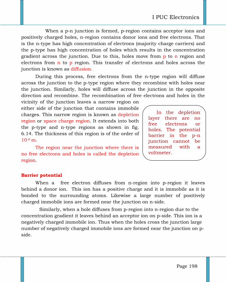
I PUC Electronics
Page 198
When a p-n junction is formed, p-region contains acceptor ions and
positively charged holes, n-region contains donor ions and free electrons. That
is the n-type has high concentration of electrons (majority charge carriers) and
the p-type has high concentration of holes which results in the concentration
gradient across the junction. Due to this, holes move from p to n region and
electrons from n to p region. This transfer of electrons and holes across the
junction is known as diffusion.
During this process, free electrons from the n-type region will diffuse
across the junction to the p-type region where they recombine with holes near
the junction. Similarly, holes will diffuse across the junction in the opposite
direction and recombine. The recombination of free electrons and holes in the
vicinity of the junction leaves a narrow region on
either side of the junction that contains immobile
charges. This narrow region is known as depletion
region or space charge region. It extends into both
the p-type and n-type regions as shown in fig.
6.14. The thickness of this region is of the order of
10-6 m.
The region near the junction where there is
no free electrons and holes is called the depletion
region.
Barrier potential
When a free electron diffuses from n-region into p-region it leaves
behind a donor ion. This ion has a positive charge and it is immobile as it is
bonded to the surrounding atoms. Likewise a large number of positively
charged immobile ions are formed near the junction on n-side.
Similarly, when a hole diffuses from p-region into n-region due to the
concentration gradient it leaves behind an acceptor ion on p-side. This ion is a
negatively charged immobile ion. Thus when the holes cross the junction large
number of negatively charged immobile ions are formed near the junction on p-
side.
In the depletion layer there are no
free electrons or holes. The potential barrier in the p-n
junction cannot be measured with a voltmeter.
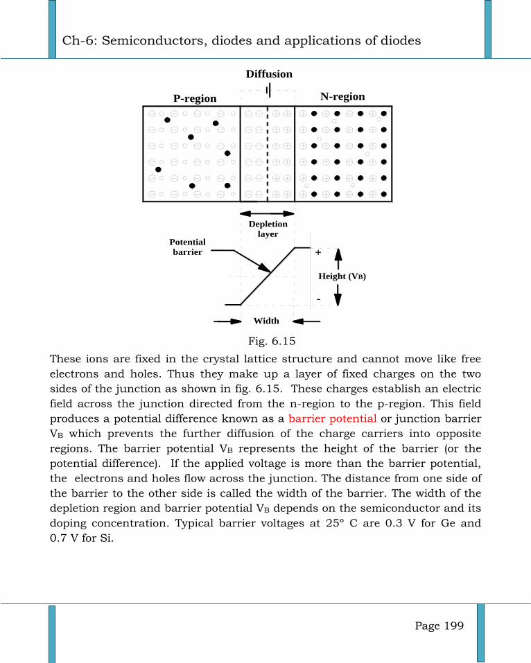
Ch-6: Semiconductors, diodes and applications of diodes
Page 199
Diffusion
N-regionP-region
Height (VB)
Depletion
layer
+
-
Width
Potential
barrier
Fig. 6.15
These ions are fixed in the crystal lattice structure and cannot move like free
electrons and holes. Thus they make up a layer of fixed charges on the two
sides of the junction as shown in fig. 6.15. These charges establish an electric
field across the junction directed from the n-region to the p-region. This field
produces a potential difference known as a barrier potential or junction barrier
VB which prevents the further diffusion of the charge carriers into opposite
regions. The barrier potential VB represents the height of the barrier (or the
potential difference). If the applied voltage is more than the barrier potential,
the electrons and holes flow across the junction. The distance from one side of
the barrier to the other side is called the width of the barrier. The width of the
depletion region and barrier potential VB depends on the semiconductor and its
doping concentration. Typical barrier voltages at 25º C are 0.3 V for Ge and
0.7 V for Si.
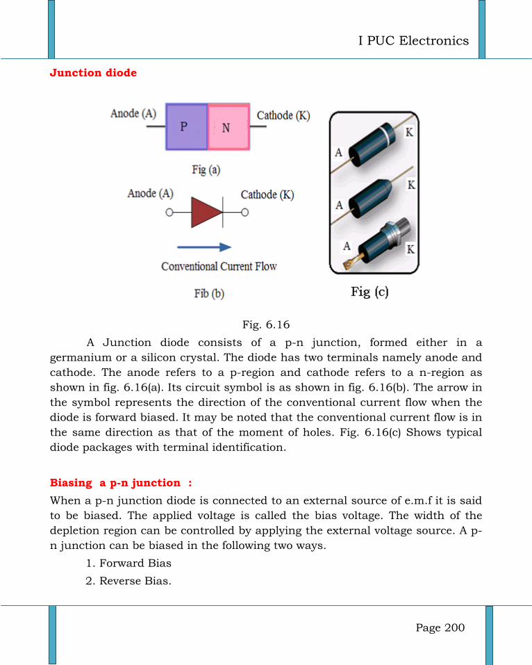
I PUC Electronics
Page 200
Junction diode
Fig. 6.16
A Junction diode consists of a p-n junction, formed either in a
germanium or a silicon crystal. The diode has two terminals namely anode and
cathode. The anode refers to a p-region and cathode refers to a n-region as
shown in fig. 6.16(a). Its circuit symbol is as shown in fig. 6.16(b). The arrow in
the symbol represents the direction of the conventional current flow when the
diode is forward biased. It may be noted that the conventional current flow is in
the same direction as that of the moment of holes. Fig. 6.16(c) Shows typical
diode packages with terminal identification.
Biasing a p-n junction :
When a p-n junction diode is connected to an external source of e.m.f it is said
to be biased. The applied voltage is called the bias voltage. The width of the
depletion region can be controlled by applying the external voltage source. A p-
n junction can be biased in the following two ways.
1. Forward Bias
2. Reverse Bias.
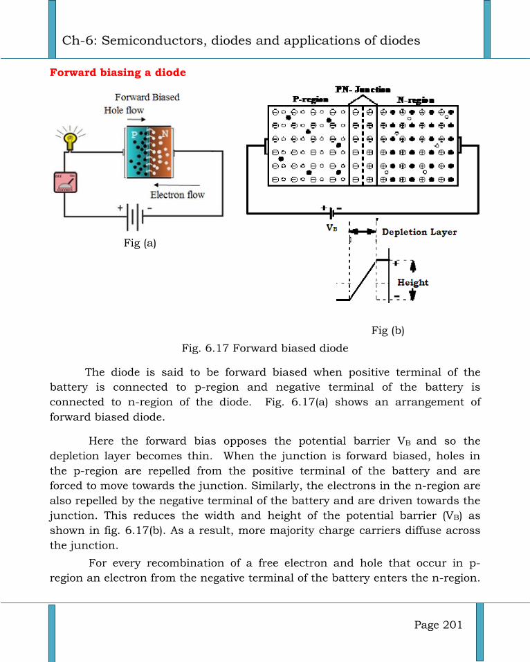
Ch-6: Semiconductors, diodes and applications of diodes
Page 201
Forward biasing a diode
Fig (a)
Fig (b)
Fig. 6.17 Forward biased diode
The diode is said to be forward biased when positive terminal of the
battery is connected to p-region and negative terminal of the battery is
connected to n-region of the diode. Fig. 6.17(a) shows an arrangement of
forward biased diode.
Here the forward bias opposes the potential barrier VB and so the
depletion layer becomes thin. When the junction is forward biased, holes in
the p-region are repelled from the positive terminal of the battery and are
forced to move towards the junction. Similarly, the electrons in the n-region are
also repelled by the negative terminal of the battery and are driven towards the
junction. This reduces the width and height of the potential barrier (VB) as
shown in fig. 6.17(b). As a result, more majority charge carriers diffuse across
the junction.
For every recombination of a free electron and hole that occur in p-
region an electron from the negative terminal of the battery enters the n-region.
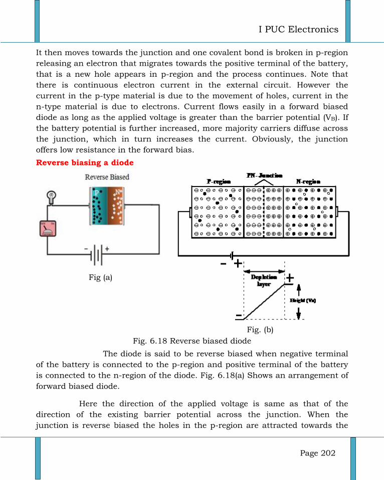
I PUC Electronics
Page 202
It then moves towards the junction and one covalent bond is broken in p-region
releasing an electron that migrates towards the positive terminal of the battery,
that is a new hole appears in p-region and the process continues. Note that
there is continuous electron current in the external circuit. However the
current in the p-type material is due to the movement of holes, current in the
n-type material is due to electrons. Current flows easily in a forward biased
diode as long as the applied voltage is greater than the barrier potential (VB). If
the battery potential is further increased, more majority carriers diffuse across
the junction, which in turn increases the current. Obviously, the junction
offers low resistance in the forward bias.
Reverse biasing a diode
Fig (a)
Fig. (b)
Fig. 6.18 Reverse biased diode
The diode is said to be reverse biased when negative terminal
of the battery is connected to the p-region and positive terminal of the battery
is connected to the n-region of the diode. Fig. 6.18(a) Shows an arrangement of
forward biased diode.
Here the direction of the applied voltage is same as that of the
direction of the existing barrier potential across the junction. When the
junction is reverse biased the holes in the p-region are attracted towards the
Ch-6: Semiconductors, diodes and applications of diodes
Page 203
negative terminal of the battery and the electrons in the n-region attracted
towards the positive terminal of the battery. Thus the majority charge carriers
are drawn away from the junction. This creates more positive ions in the n-
region and more negative ions in the p-region. This action widens the depletion
region and increases the barrier potential VB as shown in fig. 6.18(b) when
compared with the unbiased p-n junction. The barrier potential increases with
the increase in the applied voltage making it more difficult for the majority
charge carriers to diffuse across the junction. Consequently, majority charge
carriers are prevented from diffusing across the junction. Hence no current
flow through the junction when the diode is reverse biased. Thus the p-n
junction offers a very high resistance under the reverse biased condition.
Reverse saturation current (Is) or leakage current
Increase in reverse bias does not allow the majority charge carriers to diffuse
across the junction. However, this potential helps some minority carriers in
crossing the junction. Since the minority carriers in the n-region and p-region
are produced by thermally generated electron-hole pairs, these minority
carriers are extremely temperature dependent and independent of the applied
bias voltage. The applied bias voltage acts as a forward bias for these minority
carriers and a current of small magnitude flows in the external circuit in the
direction opposite to that of the conventional current due to the movement of
majority carriers. This current is known as leakage current Io or reverse
saturation current Is. For silicon it is less than 1µA and for germanium it may
exceed 10 µA. Io is found to double for every 10o C rise for Si and for every 6o C
rise in case of Ge. Large minority charge carriers are available in germanium
diode when compared to silicon diode.
Reverse breakdown
We have seen that a p-n junction allows a very small current when it is reverse
biased. This current is due to the movement of minority carriers. If the reverse
bias voltage across the junction is increased to a large value, the reverse
current through the junction increases abruptly. The voltage at which the
reverse current through the junction increases abruptly is known as reverse
break down voltage VBR. At this stage the crystal structure breaks down. Due to
I PUC Electronics
Page 204
this there is a possibility of the device to be destroyed because of overheating. If
the excess reverse voltage is removed, the crystal structure can be restored.
Junction capacitance of a diode
When the diode is reverse biased, the existing depletion region exhibits
the capacitance property due to immobile ions across the junction known as
the junction capacitance of a diode.
Transition capacitance or space charge capacitance ( CT)
In the reverse biased diode the depletion region behaves like a dielectric
medium. The depletion width (w) will increase with increased reverse bias
voltage. This capacitive effect is called transition or space charge capacitance
(CT). Capacitance ‘CT’ is related to width of depletion layer ‘w’ by the relation
CT =
Where ϵ = Permittivity of the material,
A = Surface area of the junction,
w = Width of the depletion region.
Since the width of depletion region depends on the amount of reverse
bias, capacitance CT can be controlled with the help of the applied voltage. For
a particular diode CT varies from 80 pF to less than 5 pF as reverse voltage
changes from 2 V to 15 V. This feature of the junction capacitance is utilized in
varactor diodes.
V-I characteristics
The response or behaviour of a p-n junction can be understood with the help
of V-I characteristics. The V-I characteristic is a graph of voltage applied
across the p-n junction and the current flowing through the p-n junction. An
understanding of these graphs helps to know the operation of the device.
The V-I characteristics may be divided into two parts namely
1. Forward characteristics
2. Reverse characteristics.
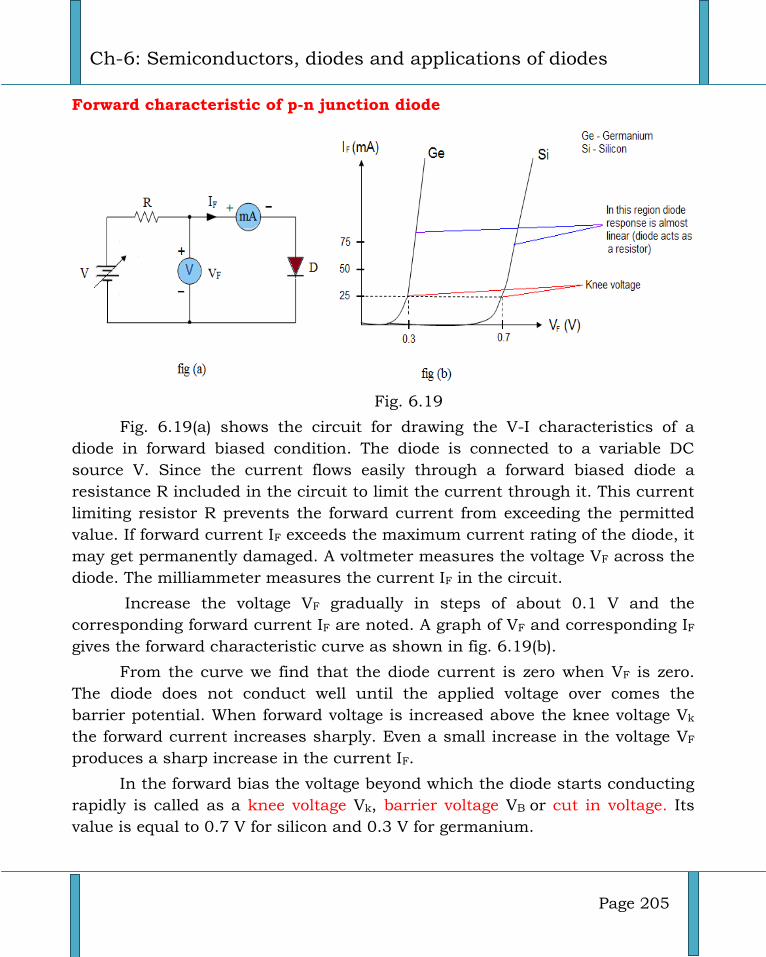
Ch-6: Semiconductors, diodes and applications of diodes
Page 205
Forward characteristic of p-n junction diode
Fig. 6.19
Fig. 6.19(a) shows the circuit for drawing the V-I characteristics of a
diode in forward biased condition. The diode is connected to a variable DC
source V. Since the current flows easily through a forward biased diode a
resistance R included in the circuit to limit the current through it. This current
limiting resistor R prevents the forward current from exceeding the permitted
value. If forward current IF exceeds the maximum current rating of the diode, it
may get permanently damaged. A voltmeter measures the voltage VF across the
diode. The milliammeter measures the current IF in the circuit.
Increase the voltage VF gradually in steps of about 0.1 V and the
corresponding forward current IF are noted. A graph of VF and corresponding IF
gives the forward characteristic curve as shown in fig. 6.19(b).
From the curve we find that the diode current is zero when VF is zero.
The diode does not conduct well until the applied voltage over comes the
barrier potential. When forward voltage is increased above the knee voltage Vk
the forward current increases sharply. Even a small increase in the voltage VF
produces a sharp increase in the current IF.
In the forward bias the voltage beyond which the diode starts conducting
rapidly is called as a knee voltage Vk, barrier voltage VB or cut in voltage. Its
value is equal to 0.7 V for silicon and 0.3 V for germanium.
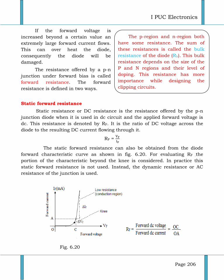
I PUC Electronics
Page 206
If the forward voltage is
increased beyond a certain value an
extremely large forward current flows.
This can over heat the diode,
consequently the diode will be
damaged.
The resistance offered by a p-n
junction under forward bias is called
forward resistance. The forward
resistance is defined in two ways.
Static forward resistance
Static resistance or DC resistance is the resistance offered by the p-n
junction diode when it is used in dc circuit and the applied forward voltage is
dc. This resistance is denoted by RF. It is the ratio of DC voltage across the
diode to the resulting DC current flowing through it.
RF =
The static forward resistance can also be obtained from the diode
forward characteristic curve as shown in fig. 6.20. For evaluating RF .the
portion of the characteristic beyond the knee is considered. In practice this
static forward resistance is not used. Instead, the dynamic resistance or AC
resistance of the junction is used.
Fig. 6.20
The p-region and n-region both
have some resistance. The sum of
these resistances is called the bulk
resistance of the diode (Rb). This bulk
resistance depends on the size of the
P and N regions and their level of
doping. This resistance has more
importance while designing the
clipping circuits.
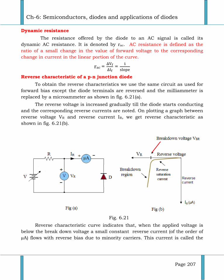
Ch-6: Semiconductors, diodes and applications of diodes
Page 207
Dynamic resistance
The resistance offered by the diode to an AC signal is called its
dynamic AC resistance. It is denoted by rac. AC resistance is defined as the
ratio of a small change in the value of forward voltage to the corresponding
change in current in the linear portion of the curve.
rac =
=
Reverse characteristic of a p-n junction diode
To obtain the reverse characteristics we use the same circuit as used for
forward bias except the diode terminals are reversed and the milliammeter is
replaced by a microammeter as shown in fig. 6.21(a).
The reverse voltage is increased gradually till the diode starts conducting
and the corresponding reverse currents are noted. On plotting a graph between
reverse voltage VR and reverse current IR, we get reverse characteristic as
shown in fig. 6.21(b).
Fig. 6.21
Reverse characteristic curve indicates that, when the applied voltage is
below the break down voltage a small constant reverse current (of the order of
µA) flows with reverse bias due to minority carriers. This current is called the
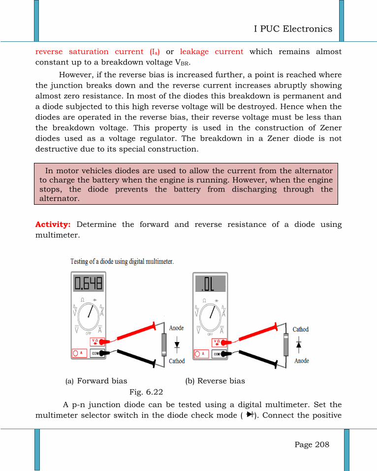
I PUC Electronics
Page 208
reverse saturation current (Is) or leakage current which remains almost
constant up to a breakdown voltage VBR.
However, if the reverse bias is increased further, a point is reached where
the junction breaks down and the reverse current increases abruptly showing
almost zero resistance. In most of the diodes this breakdown is permanent and
a diode subjected to this high reverse voltage will be destroyed. Hence when the
diodes are operated in the reverse bias, their reverse voltage must be less than
the breakdown voltage. This property is used in the construction of Zener
diodes used as a voltage regulator. The breakdown in a Zener diode is not
destructive due to its special construction.
Activity: Determine the forward and reverse resistance of a diode using
multimeter.
(a) Forward bias (b) Reverse bias
Fig. 6.22
A p-n junction diode can be tested using a digital multimeter. Set the
multimeter selector switch in the diode check mode ( ). Connect the positive
In motor vehicles diodes are used to allow the current from the alternator to charge the battery when the engine is running. However, when the engine
stops, the diode prevents the battery from discharging through the alternator.
Ch-6: Semiconductors, diodes and applications of diodes
Page 209
lead of the multimeter to the anode and negative lead to the cathode of the
diode as shown in fig. 6.22(a). If multimeter displays resistance of diode, we
can assume that the diode is good. This is the test for the diode in a forward
bias. Now connect the positive lead of the multimeter to the cathode and
negative lead to the anode as shown in fig(b). If the diode is good, multimeter
shows OL (Over Load) indicating more resistance in reverse direction.
A defective open diode indicates OL for both the forward bias and
reverse bias condition. If a diode is shorted, the meter indicates 0 V in both
forward and reverse test.
Diode equation
A diode is one of the simplest semiconductor device, which has the
characteristic of passing current in one direction only. However, unlike a
resistor, a diode does not behave linearly with respect to the applied voltage. As
the diode has an exponential V-I relationship, we cannot describe its operation
by simply using an equation of Ohm's law.
The mathematical equation which describes the exact current through a
diode, the voltage drop across the junction, the temperature of the junction,
and several physical constants is commonly known as the
Diode equation. (or Shockley’s equation)
Where
I = the diode current,
IS = the reverse saturation current
VD = the voltage across the diode
VT = the thermal voltage and
η = the ideality factor also known as the quality factor or sometimes
emission coefficient.
The ideality factor η varies from 1 to 2 depending on the fabrication
process and the semiconductor material used in many cases it is assumed to
be approximately equal to 1. For Ge diode η = 1. For Si diode η = 1 above knee
voltage and η = 2 below knee voltage.
The thermal voltage VT is defined by
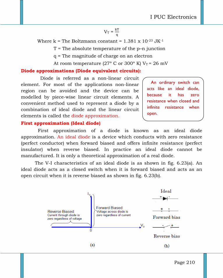
I PUC Electronics
Page 210
VT =
Where k = The Boltzmann constant = 1.381 x 10⁻²³ JK-1
T = The absolute temperature of the p–n junction
q = The magnitude of charge on an electron
At room temperature (27º C or 300º K) VT = 26 mV
Diode approximations (Diode equivalent circuits):
Diode is referred as a non-linear circuit
element. For most of the applications non-linear
region can be avoided and the device can be
modelled by piece-wise linear circuit elements. A
convenient method used to represent a diode by a
combination of ideal diode and the linear circuit
elements is called the diode approximation.
First approximation (Ideal diode)
First approximation of a diode is known as an ideal diode
approximation. An ideal diode is a device which conducts with zero resistance
(perfect conductor) when forward biased and offers infinite resistance (perfect
insulator) when reverse biased. In practice an ideal diode cannot be
manufactured. It is only a theoretical approximation of a real diode.
The V-I characteristics of an ideal diode is as shown in fig. 6.23(a). An
ideal diode acts as a closed switch when it is forward biased and acts as an
open circuit when it is reverse biased as shown in fig. 6.23(b).
An ordinary switch can
acts like an ideal diode,
because it has zero
resistance when closed and
infinite resistance when
open.
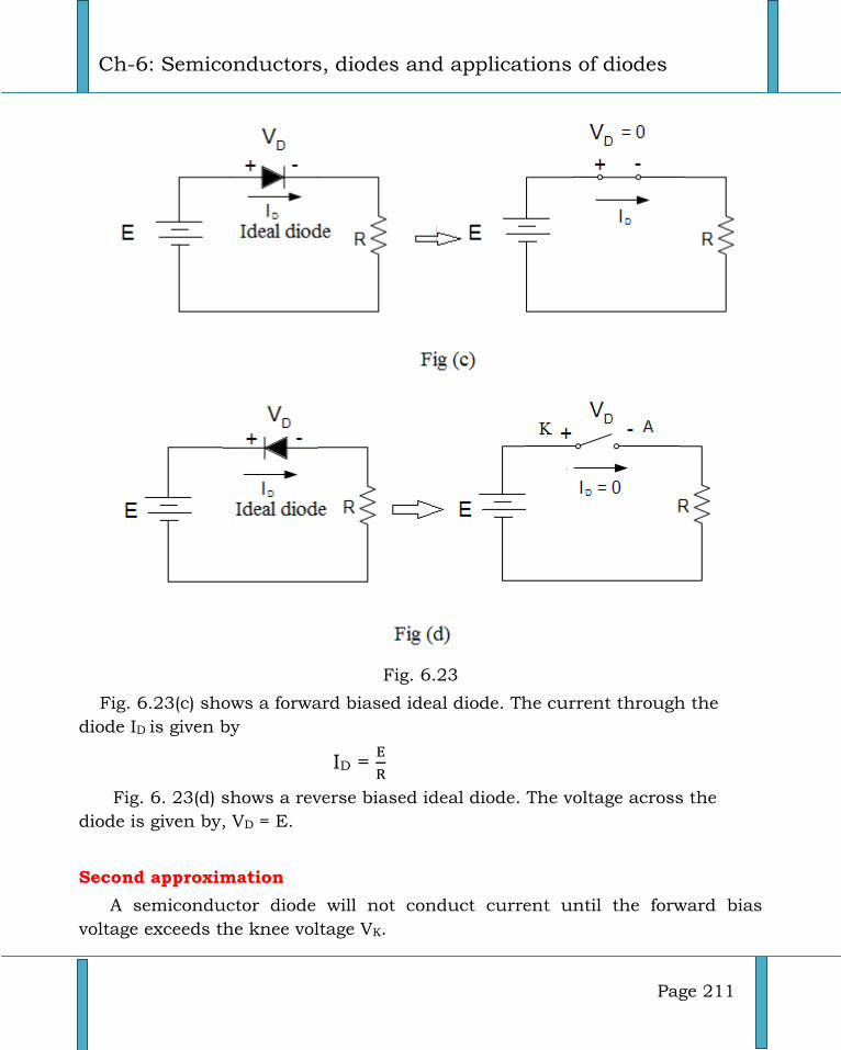
Ch-6: Semiconductors, diodes and applications of diodes
Page 211
Fig. 6.23
Fig. 6.23(c) shows a forward biased ideal diode. The current through the
diode ID is given by
ID =
Fig. 6. 23(d) shows a reverse biased ideal diode. The voltage across the
diode is given by, VD = E.
Second approximation
A semiconductor diode will not conduct current until the forward bias
voltage exceeds the knee voltage VK.
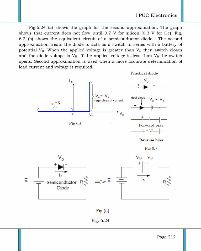
I PUC Electronics
Page 212
Fig.6.24 (a) shows the graph for the second approximation. The graph
shows that current does not flow until 0.7 V for silicon (0.3 V for Ge). Fig.
6.24(b) shows the equivalent circuit of a semiconductor diode. The second
approximation treats the diode to acts as a switch in series with a battery of
potential VB. When the applied voltage is greater than VB then switch closes
and the diode voltage is VB. If the applied voltage is less than VB the switch
opens. Second approximation is used when a more accurate determination of
load current and voltage is required.
Fig. 6.24
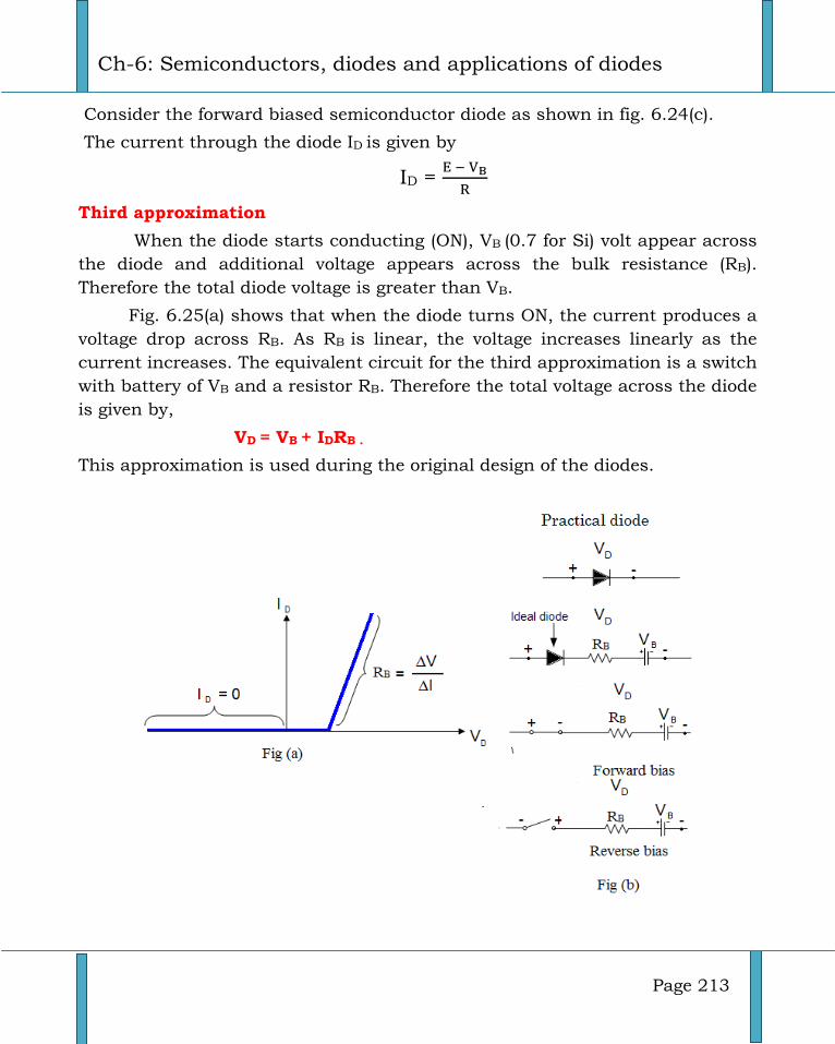
Ch-6: Semiconductors, diodes and applications of diodes
Page 213
Consider the forward biased semiconductor diode as shown in fig. 6.24(c).
The current through the diode ID is given by
ID =
Third approximation
When the diode starts conducting (ON), VB (0.7 for Si) volt appear across
the diode and additional voltage appears across the bulk resistance (RB).
Therefore the total diode voltage is greater than VB.
Fig. 6.25(a) shows that when the diode turns ON, the current produces a
voltage drop across RB. As RB is linear, the voltage increases linearly as the
current increases. The equivalent circuit for the third approximation is a switch
with battery of VB and a resistor RB. Therefore the total voltage across the diode
is given by,
VD = VB + IDRB .
This approximation is used during the original design of the diodes.
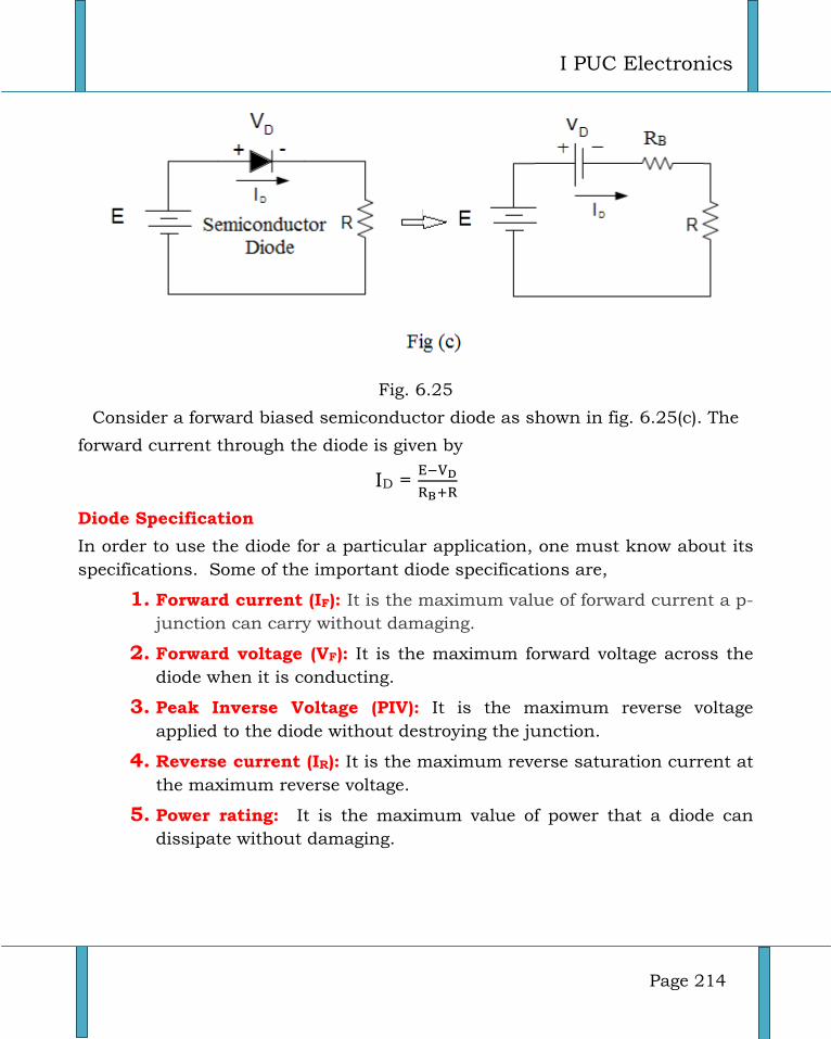
I PUC Electronics
Page 214
Fig. 6.25
Consider a forward biased semiconductor diode as shown in fig. 6.25(c). The
forward current through the diode is given by
ID =
Diode Specification
In order to use the diode for a particular application, one must know about its
specifications. Some of the important diode specifications are,
1. Forward current (IF): It is the maximum value of forward current a p-
junction can carry without damaging.
2. Forward voltage (VF): It is the maximum forward voltage across the
diode when it is conducting.
3. Peak Inverse Voltage (PIV): It is the maximum reverse voltage
applied to the diode without destroying the junction.
4. Reverse current (IR): It is the maximum reverse saturation current at
the maximum reverse voltage.
5. Power rating: It is the maximum value of power that a diode can
dissipate without damaging.
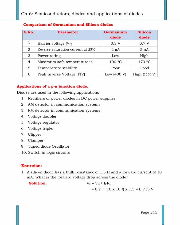
Ch-6: Semiconductors, diodes and applications of diodes
Page 215
Comparison of Germanium and Silicon diodes
Applications of a p-n junction diode.
Diodes are used in the following applications
1. Rectifiers or power diodes in DC power supplies
2. AM detector in communication systems
3. FM detector in communication systems
4. Voltage doubler
5. Voltage regulator
6. Voltage tripler
7. Clipper
8. Clamper
9. Tuned diode Oscillator
10. Switch in logic circuits
Exercise:
1. A silicon diode has a bulk resistance of 1.5 Ω and a forward current of 10
mA. What is the forward voltage drop across the diode?
Solution. VF = VB + IFRB
= 0.7 + (10 x 10-3) x 1.5 = 0.715 V
S.No. Parameter Germanium
diode
Silicon
diode
1 Barrier voltage (VB) 0.3 V 0.7 V
2 Reverse saturation current at 25ºC 2 µA 5 nA
3 Power rating Low High
4 Maximum safe temperature is 100 ºC 170 ºC
5 Temperature stability Poor Good
6 Peak Inverse Voltage (PIV) Low (400 V) High (1200 V)
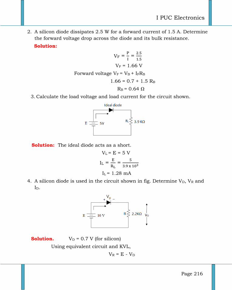
I PUC Electronics
Page 216
2. A silicon diode dissipates 2.5 W for a forward current of 1.5 A. Determine
the forward voltage drop across the diode and its bulk resistance.
Solution:
VF =
=
VF = 1.66 V
Forward voltage VF = VB + IFRB
1.66 = 0.7 + 1.5 RB
RB = 0.64 Ω
3. Calculate the load voltage and load current for the circuit shown.
Solution: The ideal diode acts as a short.
VL = E = 5 V
IL =
=
IL = 1.28 mA
4. A silicon diode is used in the circuit shown in fig. Determine VD, VR and
ID.
Solution. VD = 0.7 V (for silicon)
Using equivalent circuit and KVL,
VR = E - VD
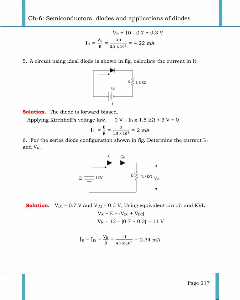
Ch-6: Semiconductors, diodes and applications of diodes
Page 217
VR = 10 - 0.7 = 9.3 V
IR =
=
= 4.22 mA
5. A circuit using ideal diode is shown in fig. calculate the current in it.
Solution. The diode is forward biased.
Applying Kirchhoff’s voltage law, 0 V – ID x 1.5 kΩ + 3 V = 0
ID =
=
= 2 mA
6. For the series diode configuration shown in fig. Determine the current ID
and VR..
Solution. VD1 = 0.7 V and VD2 = 0.3 V, Using equivalent circuit and KVL
VR = E – (VD1 + VD2)
VR = 12 – (0.7 + 0.3) = 11 V
IR = ID =
=
= 2.34 mA
I PUC Electronics
Page 218
Wave shaping circuits:
Often it is required to change the shape of the signal waveform for the
working of an electronic equipment like computer, radar, television receiver etc,
It is also necessary to generate one waveform from another circuits which
performs this job of producing waves of the desired shape are known as wave
shaping circuits. A p-n junction diode is used in non linear wave shaping
circuits. Diodes are used to perform the following two important functions
1. Clipping
2. Clamping
The non linear element used in the circuits of clipping and clamping is
the diode. Diodes are assumed to be ideal, that is the cut in voltage of the diode
is zero.
Clipping circuits.
In many applications we need to limit or control the amplitude of the
input signal. Depending on the type of limiting action the circuit is known as
limiter or clipper. A circuit used to limit the amplitude of the signal is known as
limiter. The function of a clipper circuit is to remove or clip off unwanted
portion of the input signal, such circuits are used to protect a device or circuit
from damage by a large amplitude signals. One of the most basic clipping
circuits is the half-wave rectifier.
A wave shaping circuit used to clip a portion of the input signal without
distorting the remaining part of the waveform is called a clipping circuit or
clipper.
Series positive clipper
The clipper which removes positive half cycles of the input voltage is called the
positive clipper.
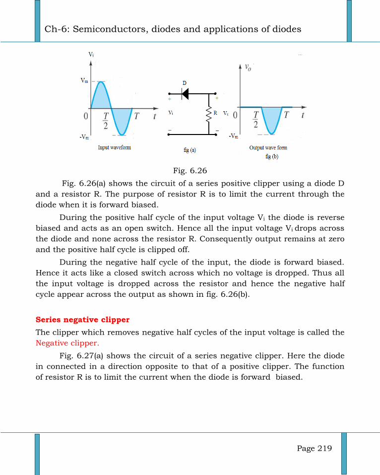
Ch-6: Semiconductors, diodes and applications of diodes
Page 219
Fig. 6.26
Fig. 6.26(a) shows the circuit of a series positive clipper using a diode D
and a resistor R. The purpose of resistor R is to limit the current through the
diode when it is forward biased.
During the positive half cycle of the input voltage Vi the diode is reverse
biased and acts as an open switch. Hence all the input voltage Vi drops across
the diode and none across the resistor R. Consequently output remains at zero
and the positive half cycle is clipped off.
During the negative half cycle of the input, the diode is forward biased.
Hence it acts like a closed switch across which no voltage is dropped. Thus all
the input voltage is dropped across the resistor and hence the negative half
cycle appear across the output as shown in fig. 6.26(b).
Series negative clipper
The clipper which removes negative half cycles of the input voltage is called the
Negative clipper.
Fig. 6.27(a) shows the circuit of a series negative clipper. Here the diode
in connected in a direction opposite to that of a positive clipper. The function
of resistor R is to limit the current when the diode is forward biased.
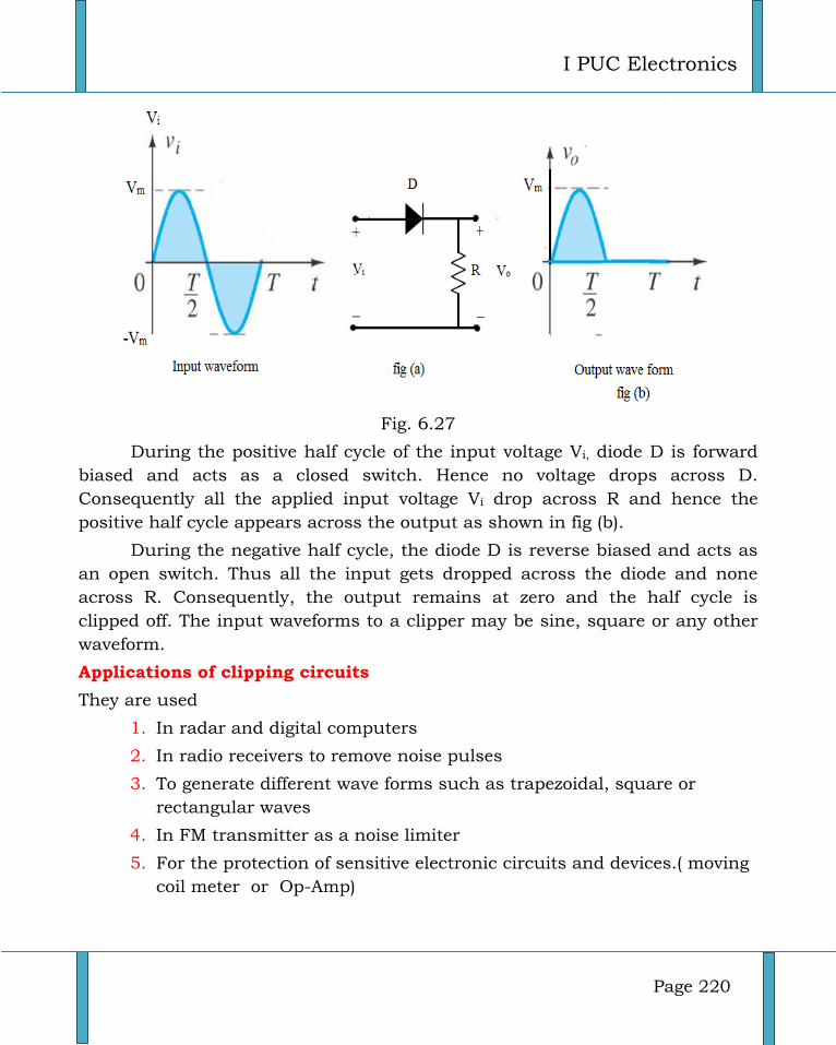
I PUC Electronics
Page 220
Fig. 6.27
During the positive half cycle of the input voltage Vi, diode D is forward
biased and acts as a closed switch. Hence no voltage drops across D.
Consequently all the applied input voltage Vi drop across R and hence the
positive half cycle appears across the output as shown in fig (b).
During the negative half cycle, the diode D is reverse biased and acts as
an open switch. Thus all the input gets dropped across the diode and none
across R. Consequently, the output remains at zero and the half cycle is
clipped off. The input waveforms to a clipper may be sine, square or any other
waveform.
Applications of clipping circuits
They are used
1. In radar and digital computers
2. In radio receivers to remove noise pulses
3. To generate different wave forms such as trapezoidal, square or
rectangular waves
4. In FM transmitter as a noise limiter
5. For the protection of sensitive electronic circuits and devices.( moving
coil meter or Op-Amp)
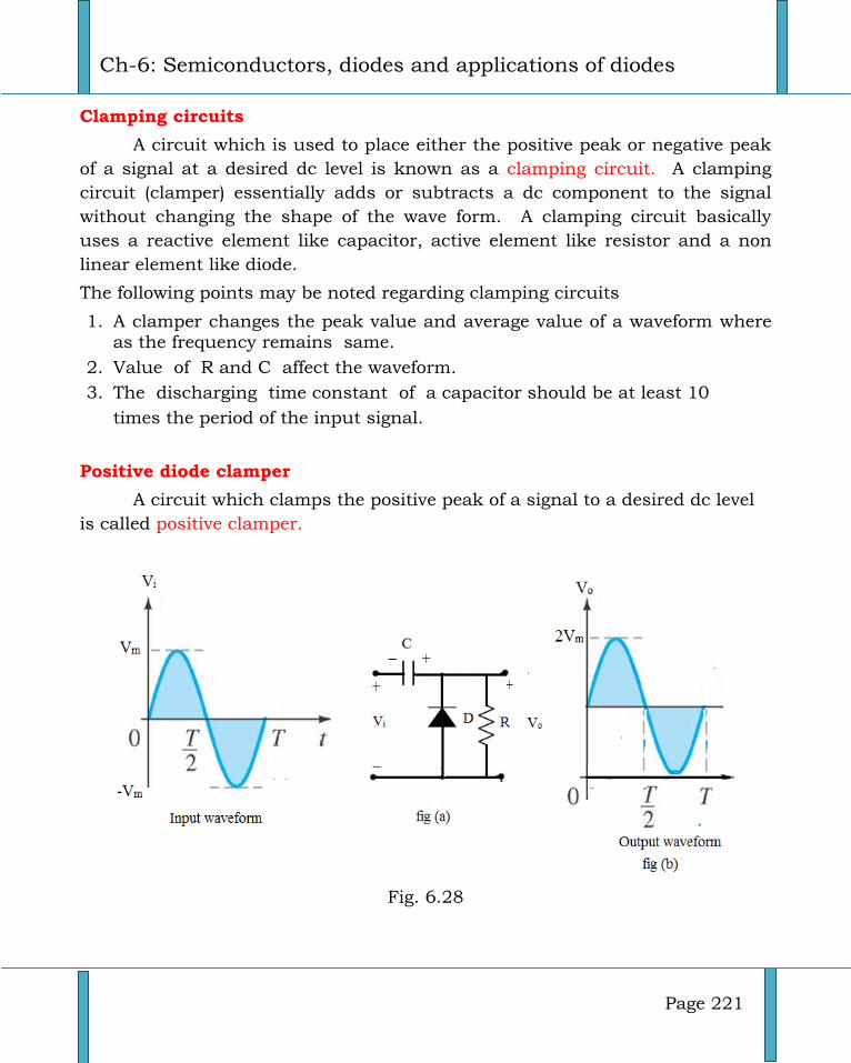
Ch-6: Semiconductors, diodes and applications of diodes
Page 221
Clamping circuits
A circuit which is used to place either the positive peak or negative peak
of a signal at a desired dc level is known as a clamping circuit. A clamping
circuit (clamper) essentially adds or subtracts a dc component to the signal
without changing the shape of the wave form. A clamping circuit basically
uses a reactive element like capacitor, active element like resistor and a non
linear element like diode.
The following points may be noted regarding clamping circuits
1. A clamper changes the peak value and average value of a waveform where as the frequency remains same.
2. Value of R and C affect the waveform.
3. The discharging time constant of a capacitor should be at least 10
times the period of the input signal.
Positive diode clamper
A circuit which clamps the positive peak of a signal to a desired dc level
is called positive clamper.
Fig. 6.28
I PUC Electronics
Page 222
Fig. 6.28(a) shows the circuit of a positive clamper. The discharge path
for the capacitor is provided by a resistor R. The values of C and R (τ = CR) are
so chosen that the discharge time should be very large. In other words the
voltage across the capacitor will not discharge significantly during the non
conducting state of the diode.
During the negative half cycle of input Vi, the diode is forward biased
and behaves as a short. Thus the resistor R (parallel to D) also gets shorted.
Consequently during this negative half cycle the capacitor is charged to Vm.
with a polarity as shown in fig. 6.28(b).
During the positive half cycle, the diode becomes reverse biased and acts
as an open circuit. Thus there will be no effect on the capacitor voltage. Also R
has a very high resistance, so that it cannot discharge significantly during the
positive half cycle. Thus the capacitor acts as a battery of voltage Vm. Hence
during the positive half cycle, output voltage will be the sum of the input
voltage and the capacitive voltage. Since the polarity of the voltage on the
capacitor is the same as the input (positive), Hence the peak amplitude of the
output is
Vom = Vm + (Vm) = 2Vm .
From the output waveform, it is clear that the output has been positively
clamped.
Negative diode clamper
A circuit which clamps the negative peak of a signal to a desired dc level
is called negative clamper.
Fig. 6.29(a) shows circuit of a negative diode clamper. It consists of a
diode D and a capacitor C connected as positive clamper. The only difference in
the circuit is that the polarity of the diode is reversed.
During the positive half cycle of the input signal, the diode is forward
biased and allows the capacitor C to charge towards the maximum input
voltage Vm.
During the negative half cycle, the diode is reverse biased and acts as an
open switch. As the discharge time constant of the capacitor is much greater
than the time period of the input signal, the capacitor cannot discharge and
serves as a battery of voltage -Vm. Therefore the output voltage will be equal to
the sum of ac input signal and the capacitor voltage -Vm. The polarity of the
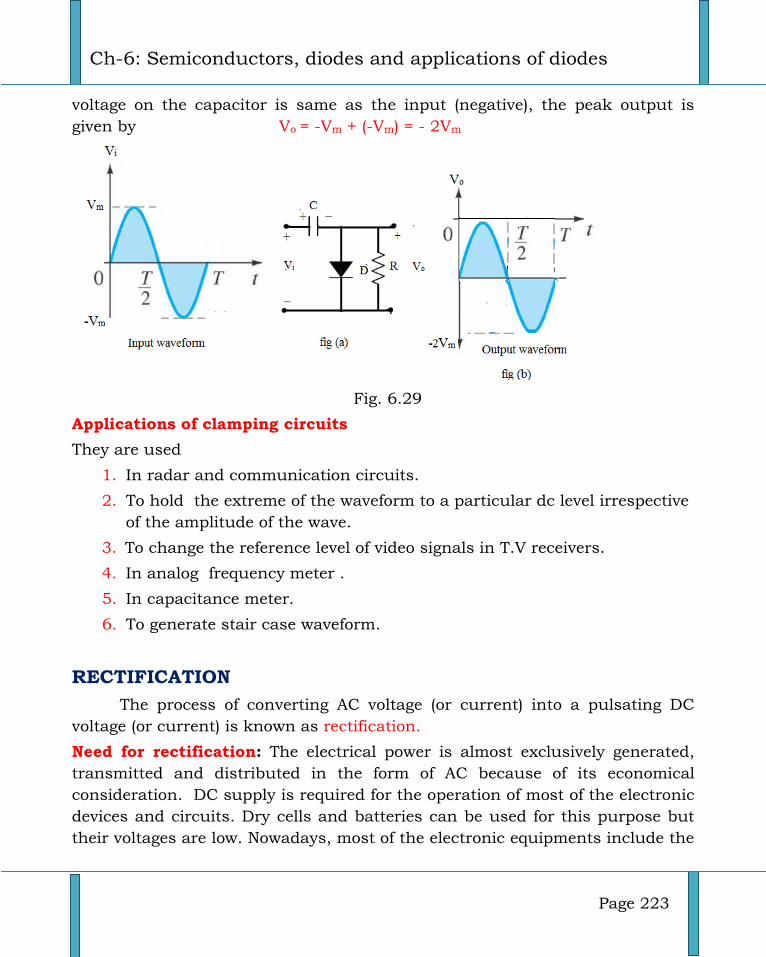
Ch-6: Semiconductors, diodes and applications of diodes
Page 223
voltage on the capacitor is same as the input (negative), the peak output is
given by Vo = -Vm + (-Vm) = - 2Vm
Fig. 6.29
Applications of clamping circuits
They are used
1. In radar and communication circuits.
2. To hold the extreme of the waveform to a particular dc level irrespective
of the amplitude of the wave.
3. To change the reference level of video signals in T.V receivers.
4. In analog frequency meter .
5. In capacitance meter.
6. To generate stair case waveform.
RECTIFICATION
The process of converting AC voltage (or current) into a pulsating DC
voltage (or current) is known as rectification.
Need for rectification: The electrical power is almost exclusively generated,
transmitted and distributed in the form of AC because of its economical
consideration. DC supply is required for the operation of most of the electronic
devices and circuits. Dry cells and batteries can be used for this purpose but
their voltages are low. Nowadays, most of the electronic equipments include the
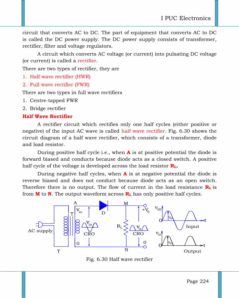
I PUC Electronics
Page 224
circuit that converts AC to DC. The part of equipment that converts AC to DC
is called the DC power supply. The DC power supply consists of transformer,
rectifier, filter and voltage regulators.
A circuit which converts AC voltage (or current) into pulsating DC voltage
(or current) is called a rectifier.
There are two types of rectifier, they are
1. Half wave rectifier (HWR)
2. Full wave rectifier (FWR)
There are two types in full wave rectifiers
1. Centre-tapped FWR
2. Bridge rectifier
Half Wave Rectifier
A rectifier circuit which rectifies only one half cycles (either positive or
negative) of the input AC wave is called half wave rectifier. Fig. 6.30 shows the
circuit diagram of a half wave rectifier, which consists of a transformer, diode
and load resistor.
During positive half cycle i.e., when A is at positive potential the diode is
forward biased and conducts because diode acts as a closed switch. A positive
half cycle of the voltage is developed across the load resistor RL.
During negative half cycles, when A is at negative potential the diode is
reverse biased and does not conduct because diode acts as an open switch.
Therefore there is no output. The flow of current in the load resistance RL is
from M to N. The output waveform across RL has only positive half cycles.
AC supply
D
0
CRO
T
CRO
Input
vin
vo
Output
vmt
t
0
0vm
v0
vin
vin
T
0
+V0
R L
A M
N
Fig. 6.30 Half wave rectifier
Ch-6: Semiconductors, diodes and applications of diodes
Page 225
Peak Inverse Voltage (PIV)
PIV is the maximum voltage the rectifying diode can withstand, when it is
reverse biased.
During the negative half cycles of the input voltage, the diode is reverse
biased, current doesn’t flow through the load resistance RL, hence there is no
drop across the load resistance RL. Consequently the whole of the input voltage
appears across the diode. Thus the maximum voltage which appears across the
diode is equal to the peak value of the secondary voltage. PIV = Vm.
Peak current Im =
Where RF is the forward resistance of the diode and RL is the load resistance.
DC value or Average value
Vav = Vdc =
= 0. 318 Vm
Where Vav is the average DC voltage across the load and Vm is the peak value of
voltage,
Iav = Idc =
= 0. 318 Im
Where Iav is the average dc current flowing through the load RL and Im is the
peak value of current.
RMS value: Vrms =
and Irms =
=
Where Vrms and Irms are the root mean square values of voltage and current.
Ripple Factor: Ripple factor ( ) is the ratio of the rms value of the AC
component of the load voltage to the average value of load voltage.
γ =
=
= √[
]
= 1.21 for HWR
Rectification Efficiency
It is defined as the ratio of dc output power Pdc to the ac input power Pac,
is given as
η =
=
= 0.406 or 40.6%
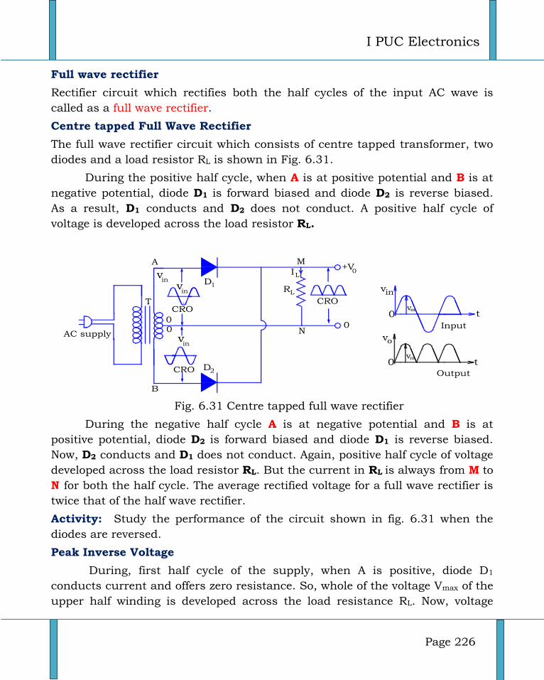
I PUC Electronics
Page 226
Full wave rectifier
Rectifier circuit which rectifies both the half cycles of the input AC wave is
called as a full wave rectifier.
Centre tapped Full Wave Rectifier
The full wave rectifier circuit which consists of centre tapped transformer, two
diodes and a load resistor RL is shown in Fig. 6.31.
During the positive half cycle, when A is at positive potential and B is at
negative potential, diode D1 is forward biased and diode D2 is reverse biased.
As a result, D1 conducts and D2 does not conduct. A positive half cycle of
voltage is developed across the load resistor RL.
CRO
vin
0
D 1
D 2
CRO
vin
AC supply
0
CRO
Input
vin
vo
Output
vmt
t
0
0vm
vin
T
0
+V0
R L
A M
N
B
IL
Fig. 6.31 Centre tapped full wave rectifier
During the negative half cycle A is at negative potential and B is at
positive potential, diode D2 is forward biased and diode D1 is reverse biased.
Now, D2 conducts and D1 does not conduct. Again, positive half cycle of voltage
developed across the load resistor RL. But the current in RL is always from M to
N for both the half cycle. The average rectified voltage for a full wave rectifier is
twice that of the half wave rectifier.
Activity: Study the performance of the circuit shown in fig. 6.31 when the
diodes are reversed.
Peak Inverse Voltage
During, first half cycle of the supply, when A is positive, diode D1
conducts current and offers zero resistance. So, whole of the voltage Vmax of the
upper half winding is developed across the load resistance RL. Now, voltage
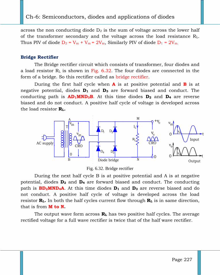
Ch-6: Semiconductors, diodes and applications of diodes
Page 227
across the non conducting diode D2 is the sum of voltage across the lower half
of the transformer secondary and the voltage across the load resistance RL.
Thus PIV of diode D2 = Vm + Vm = 2Vm, Similarly PIV of diode D1 = 2Vm.
Bridge Rectifier
The Bridge rectifier circuit which consists of transformer, four diodes and
a load resistor RL is shown in Fig. 6.32. The four diodes are connected in the
form of a bridge. So this rectifier called as bridge rectifier.
During the first half cycle when A is at positive potential and B is at
negative potential, diodes D1 and D3 are forward biased and conduct. The
conducting path is AD1MND3B. At this time diodes D2 and D4 are reverse
biased and do not conduct. A positive half cycle of voltage is developed across
the load resistor RL.
AC supply
Diode bridge
0
CROCRO
Input
vin
vo
Output
vmt
t
0
0vm
v0
RL
D1
D3
D2
D4
vin
vin
T IL
0
+v0
M
N
A
B
Fig. 6.32. Bridge rectifier
During the next half cycle B is at positive potential and A is at negative
potential, diodes D2 and D4 are forward biased and conduct. The conducting
path is BD2MND4A. At this time diodes D1 and D3 are reverse biased and do
not conduct. A positive half cycle of voltage is developed across the load
resistor RL. In both the half cycles current flow through RL is in same direction,
that is from M to N.
The output wave form across RL has two positive half cycles. The average
rectified voltage for a full wave rectifier is twice that of the half wave rectifier.
I PUC Electronics
Page 228
Peak Inverse Voltage
When A is positive diode D1 and D3 are conducting whereas D2 and D4
are non conducting being reverse biased. The conducting diodes D1 and D3
offers zero resistance. The entire voltage of the transformer secondary winding,
Vmax is developed across the load resistance RL. The same voltage Vmax acts
across the each non-conducting diodes D2 and D4. Thus PIV = Vm
Parameters of centre tapped Full wave rectifier and Bridge rectifier
Peak current: Peak value of current flowing through the load resistance RL in
case of centre tapped rectifier is given as
Peak current of a centre tapped rectifier Im =
Peak value of current flowing through the load resistance RL in case of bridge
rectifier is given as
Peak current for bridge rectifier Im =
Average Value or DC Value:
Vav = Vdc =
= 0.636Vm
Where Vav is the average D.C. voltage across the load and Vm is the peak value
of voltage.
Iav = Idc =
=
= 0.636 Im
Where Iav is the average D.C. current flowing through the load RL and Im is the
peak value of current.
RMS Value: Vrms =
√ , and Irms =
√ =
√
Where Vrms and Irms are the root mean square value of voltage and current.
Ripple Factor: Ripple factor () is the ratio of the rms value of the AC
component of the load voltage to the average value of load voltage.
γ =
=
= √[
]
= 0.48 for FWR
Ch-6: Semiconductors, diodes and applications of diodes
Page 229
Efficiency: The ratio of the output DC power to the input ac power is called
efficiency , is given by
η =
=
= 0.812 or 81.2%
Voltage Regulation
The degree at which a power supply varies in its output voltage under
conditions of load variations is measured by the voltage regulation which is
usually expressed as percentage. In an unregulated power supply, output
voltage changes whenever input supply or load resistance changes. The change
in voltage from no-load to full-load condition is called ‘ voltage regulation’.
Percentage regulation =
x 100%
Where VNL = No-load or open circuit terminal voltage of the supply.
VFL = Full-load terminal voltage of the supply.
Comparison of rectifiers
Negative voltage rectifier
Some circuits like operational amplifiers work with positive and negative
power supply together. It is necessary to understand the working of negative
voltage rectifiers. Negative rectifier supply is similar to positive rectifier supply.
The difference is that the way by which we choose the reference terminal. If
Particulars Half wave rectifier
Centre tapped rectifier
Bridge rectifier
1. Number of diodes 1 2 4
2. PIV Vm 2Vm Vm
3. DC voltage (Vdc)
4. RMS values of voltage (Vrms)
√
√
5. RMS values of current (Irms)
√
√
6. Ripple factor () 1.21 0.48 0.48
7. Efficiency () = 40. 6 % = 81.2 % = 81.2 %
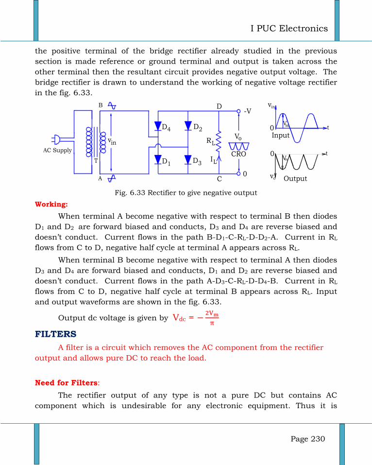
I PUC Electronics
Page 230
the positive terminal of the bridge rectifier already studied in the previous
section is made reference or ground terminal and output is taken across the
other terminal then the resultant circuit provides negative output voltage. The
bridge rectifier is drawn to understand the working of negative voltage rectifier
in the fig. 6.33.
B
A
T
vin
D 1
D 2
D 3
D 4
R L
I L
C
D-V
0
CRO
V o
v in
V m
m
Output
Input
V
v o
0
0 t
t
Fig. 6.33 Rectifier to give negative output
Working:
When terminal A become negative with respect to terminal B then diodes
D1 and D2 are forward biased and conducts, D3 and D4 are reverse biased and
doesn’t conduct. Current flows in the path B-D1-C-RL-D-D2-A. Current in RL
flows from C to D, negative half cycle at terminal A appears across RL.
When terminal B become negative with respect to terminal A then diodes
D3 and D4 are forward biased and conducts, D1 and D2 are reverse biased and
doesn’t conduct. Current flows in the path A-D3-C-RL-D-D4-B. Current in RL
flows from C to D, negative half cycle at terminal B appears across RL. Input
and output waveforms are shown in the fig. 6.33.
Output dc voltage is given by Vdc =
FILTERS
A filter is a circuit which removes the AC component from the rectifier
output and allows pure DC to reach the load.
Need for Filters:
The rectifier output of any type is not a pure DC but contains AC
component which is undesirable for any electronic equipment. Thus it is
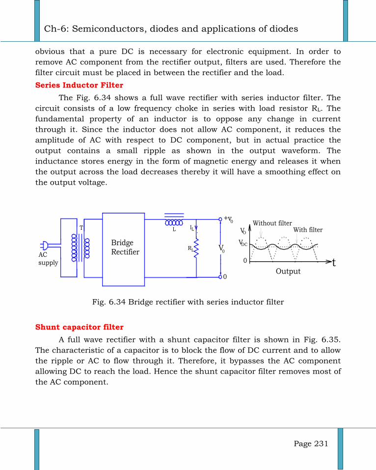
Ch-6: Semiconductors, diodes and applications of diodes
Page 231
obvious that a pure DC is necessary for electronic equipment. In order to
remove AC component from the rectifier output, filters are used. Therefore the
filter circuit must be placed in between the rectifier and the load.
Series Inductor Filter
The Fig. 6.34 shows a full wave rectifier with series inductor filter. The
circuit consists of a low frequency choke in series with load resistor RL. The
fundamental property of an inductor is to oppose any change in current
through it. Since the inductor does not allow AC component, it reduces the
amplitude of AC with respect to DC component, but in actual practice the
output contains a small ripple as shown in the output waveform. The
inductance stores energy in the form of magnetic energy and releases it when
the output across the load decreases thereby it will have a smoothing effect on
the output voltage.
ACsupply
BridgeRectifier
VO
Outputt0
V0
RL
T IL
0
+v0
VDC
L With filterWithout filter
Fig. 6.34 Bridge rectifier with series inductor filter
Shunt capacitor filter
A full wave rectifier with a shunt capacitor filter is shown in Fig. 6.35.
The characteristic of a capacitor is to block the flow of DC current and to allow
the ripple or AC to flow through it. Therefore, it bypasses the AC component
allowing DC to reach the load. Hence the shunt capacitor filter removes most of
the AC component.
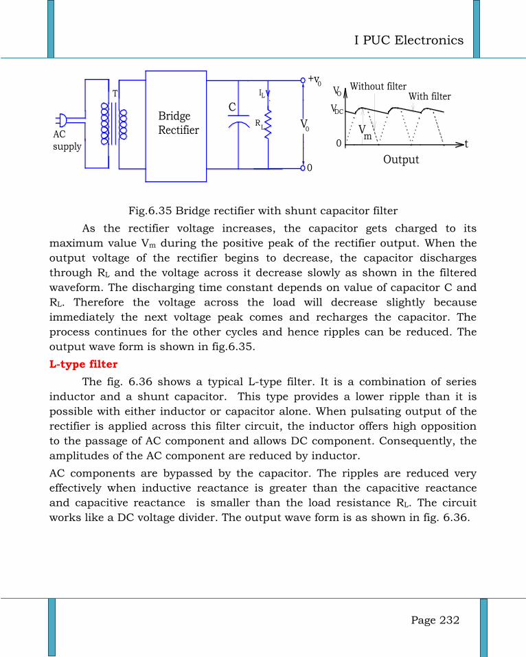
I PUC Electronics
Page 232
ACsupply
BridgeRectifier
VO
Output
t0
V0
RL
T IL
0
+v0
VDC
With filterWithout filter
C
Vm
Fig.6.35 Bridge rectifier with shunt capacitor filter
As the rectifier voltage increases, the capacitor gets charged to its
maximum value Vm during the positive peak of the rectifier output. When the
output voltage of the rectifier begins to decrease, the capacitor discharges
through RL and the voltage across it decrease slowly as shown in the filtered
waveform. The discharging time constant depends on value of capacitor C and
RL. Therefore the voltage across the load will decrease slightly because
immediately the next voltage peak comes and recharges the capacitor. The
process continues for the other cycles and hence ripples can be reduced. The
output wave form is shown in fig.6.35.
L-type filter
The fig. 6.36 shows a typical L-type filter. It is a combination of series
inductor and a shunt capacitor. This type provides a lower ripple than it is
possible with either inductor or capacitor alone. When pulsating output of the
rectifier is applied across this filter circuit, the inductor offers high opposition
to the passage of AC component and allows DC component. Consequently, the
amplitudes of the AC component are reduced by inductor.
AC components are bypassed by the capacitor. The ripples are reduced very
effectively when inductive reactance is greater than the capacitive reactance
and capacitive reactance is smaller than the load resistance RL. The circuit
works like a DC voltage divider. The output wave form is as shown in fig. 6.36.
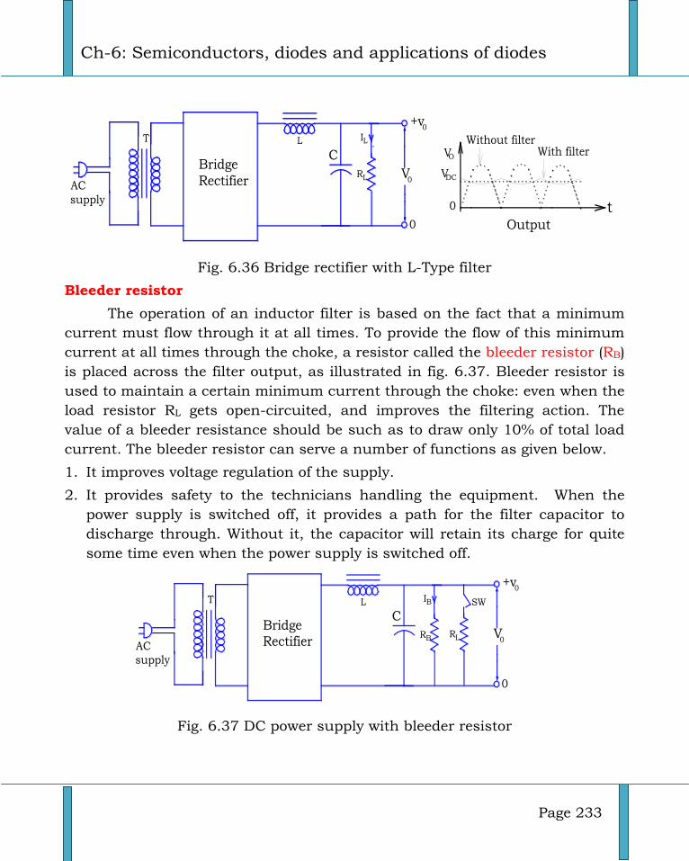
Ch-6: Semiconductors, diodes and applications of diodes
Page 233
ACsupply
BridgeRectifier
VO
Output
t0
V0
RL
T IL
0
+v0
VDC
LWith filter
Without filter
C
Fig. 6.36 Bridge rectifier with L-Type filter
Bleeder resistor
The operation of an inductor filter is based on the fact that a minimum
current must flow through it at all times. To provide the flow of this minimum
current at all times through the choke, a resistor called the bleeder resistor (RB)
is placed across the filter output, as illustrated in fig. 6.37. Bleeder resistor is
used to maintain a certain minimum current through the choke: even when the
load resistor RL gets open-circuited, and improves the filtering action. The
value of a bleeder resistance should be such as to draw only 10% of total load
current. The bleeder resistor can serve a number of functions as given below.
1. It improves voltage regulation of the supply.
2. It provides safety to the technicians handling the equipment. When the
power supply is switched off, it provides a path for the filter capacitor to
discharge through. Without it, the capacitor will retain its charge for quite
some time even when the power supply is switched off.
ACsupply
BridgeRectifier
RB
T IBL
C
V0
RL
0
+v0
SW
Fig. 6.37 DC power supply with bleeder resistor
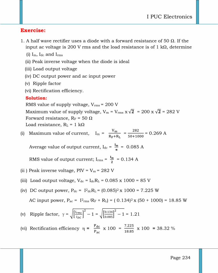
I PUC Electronics
Page 234
Exercise:
1. A half wave rectifier uses a diode with a forward resistance of 50 Ω. If the
input ac voltage is 200 V rms and the load resistance is of 1 kΩ, determine
(i) Im, Idc and Irms
(ii) Peak inverse voltage when the diode is ideal
(iii) Load output voltage
(iv) DC output power and ac input power
(v) Ripple factor
(vi) Rectification efficiency.
Solution:
RMS value of supply voltage, Vrms = 200 V
Maximum value of supply voltage, Vm = Vrms x √ = 200 x √ = 282 V
Forward resistance, RF = 50 Ω
Load resistance, RL = 1 kΩ
(i) Maximum value of current, Im =
=
= 0.269 A
Average value of output current, Idc =
= 0.085 A
RMS value of output current; Irms =
= 0.134 A
(ii ) Peak inverse voltage, PIV = Vm = 282 V
(iii) Load output voltage, Vdc = IdcRL = 0.085 x 1000 = 85 V
(iv) DC output power, Pdc = I2dcRL = (0.085)2 x 1000 = 7.225 W
AC input power, Pac = I2rms
(RF + RL) = ( 0.134)2 x (50 + 1000) = 18.85 W
(v) Ripple factor, = √[
]
= √[
]
= 1.21
(vi) Rectification efficiency =
x 100 =
x 100 = 38.32 %
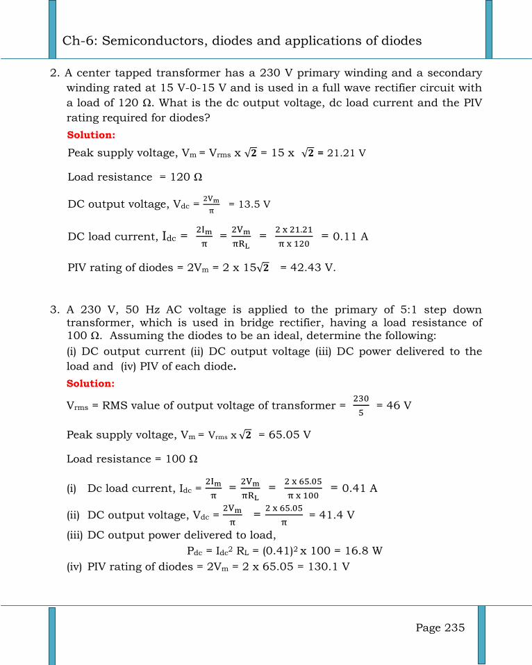
Ch-6: Semiconductors, diodes and applications of diodes
Page 235
2. A center tapped transformer has a 230 V primary winding and a secondary
winding rated at 15 V-0-15 V and is used in a full wave rectifier circuit with
a load of 120 Ω. What is the dc output voltage, dc load current and the PIV
rating required for diodes?
Solution:
Peak supply voltage, Vm = Vrms x √ = 15 x √ = 21.21 V
Load resistance = 120 Ω
DC output voltage, Vdc =
= 13.5 V
DC load current, Idc =
=
=
= 0.11 A
PIV rating of diodes = 2Vm = 2 x 15√ = 42.43 V.
3. A 230 V, 50 Hz AC voltage is applied to the primary of 5:1 step down transformer, which is used in bridge rectifier, having a load resistance of 100 Ω. Assuming the diodes to be an ideal, determine the following:
(i) DC output current (ii) DC output voltage (iii) DC power delivered to the
load and (iv) PIV of each diode.
Solution:
Vrms = RMS value of output voltage of transformer =
= 46 V
Peak supply voltage, Vm = Vrms x √ = 65.05 V
Load resistance = 100 Ω
(i) Dc load current, Idc =
=
=
= 0.41 A
(ii) DC output voltage, Vdc =
=
= 41.4 V
(iii) DC output power delivered to load,
Pdc = Idc2 RL = (0.41)2 x 100 = 16.8 W
(iv) PIV rating of diodes = 2Vm = 2 x 65.05 = 130.1 V
I PUC Electronics
Page 236
4. The DC voltage supply provides 50 V when the output is unloaded. When
connected to a load the output drops to 46 V. Calculate the value of voltage
regulation.
Solution:
No load voltage , VNL = 50 V
Full load voltage, VFL = 46 V
Percentage regulation =
x 100% =
x 100% =8.69%
Special Diodes :
There are a number of two terminal semiconductor devices having a
single p-n junction like the semiconductor diode, but they are different from
one another based on their operation, application etc. They are,
1. Zener diode
2. Light emitting diode
3. Varactor diode
4. IR emitter diode
5. Photo diode
6. Tunnel diode
7. Schottky diode
Zener diode
Zener diode is a special purpose semiconductor diode always used in
reverse bias with a specific reverse breakdown voltage. It is named after C.A.
Zener who analyzed the voltage breakdown of insulators. Silicon is preferred
over germanium because of its higher temperature and current capability. The
breakdown or Zener voltage (VZ) depends upon the amount of doping.
Breakdown occurs due to both Zener effect and avalanche effect.
Zener diode is a heavily doped semiconductor diode. Since doping level is
high, the p-n junction becomes narrow and thereby the electric field in the
depletion layer increases. When the reverse bias is increased, the electric field
at the junction becomes large enough to break covalent bonds and generate
electron hole pairs. Consequently reverse current rises abruptly. Such a
phenomenon is called Zener breakdown. The process by which covalent bonds
in the depletion region are directly broken by a strong electric field is called
Ch-6: Semiconductors, diodes and applications of diodes
Page 237
Zener breakdown. The reverse voltage at which the Zener breakdown takes
place is called Zener breakdown voltage. By varying the amount of doping, it is
possible to produce Zener diodes with breakdown voltages from about 2 V to
200 V.
A Zener diode is also called as a voltage reference, voltage regulator or
breakdown diode. The schematic symbol and its equivalent circuit are as
shown in fig. 6.38.
R ZV Z
Symbol Equivalent circuit
Fig.6.38 Zener diode symbol with equivalent circuit
Avalanche breakdown and Zener breakdown
If the reverse bias of a p-n junction is made high, at a certain voltage the
junction breaks down and the current through the junction increases sharply.
The voltage at which this phenomenon occurs is called breakdown voltage. The
breakdown voltage depends on the doping level. There are two processes by
which breakdown occurs. They are:
1. Avalanche breakdown
2. Zener breakdown
Avalanche breakdown
This type of breakdown occurs in lightly doped diodes. Lightly doped
diodes have wide depletion region. The increased reverse voltage increases the
velocities of minority charge carriers (thermally generated). These highly
accelerated carriers collide with the atoms in the depletion region. The covalent
bonds are broken and new electron hole pairs are generated. These new
minority carriers also pick up sufficient energy from the applied field, collide
with other atoms and generate more charge carriers. This process is
cummulative and a large number of carriers are generated. This causes a high
reverse current to flow. This mechanism of breakdown is known as avalanche
breakdown.
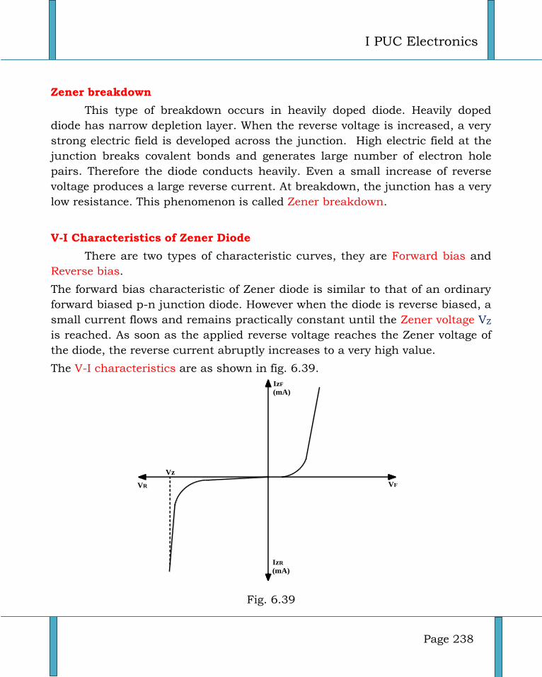
I PUC Electronics
Page 238
Zener breakdown
This type of breakdown occurs in heavily doped diode. Heavily doped
diode has narrow depletion layer. When the reverse voltage is increased, a very
strong electric field is developed across the junction. High electric field at the
junction breaks covalent bonds and generates large number of electron hole
pairs. Therefore the diode conducts heavily. Even a small increase of reverse
voltage produces a large reverse current. At breakdown, the junction has a very
low resistance. This phenomenon is called Zener breakdown.
V-I Characteristics of Zener Diode
There are two types of characteristic curves, they are Forward bias and
Reverse bias.
The forward bias characteristic of Zener diode is similar to that of an ordinary
forward biased p-n junction diode. However when the diode is reverse biased, a
small current flows and remains practically constant until the Zener voltage VZ
is reached. As soon as the applied reverse voltage reaches the Zener voltage of
the diode, the reverse current abruptly increases to a very high value.
The V-I characteristics are as shown in fig. 6.39.
VF VR
IzR
(mA)
Vz
IzF
(mA)
Fig. 6.39
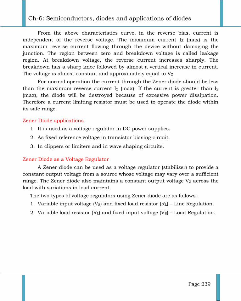
Ch-6: Semiconductors, diodes and applications of diodes
Page 239
From the above characteristics curve, in the reverse bias, current is
independent of the reverse voltage. The maximum current IZ (max) is the
maximum reverse current flowing through the device without damaging the
junction. The region between zero and breakdown voltage is called leakage
region. At breakdown voltage, the reverse current increases sharply. The
breakdown has a sharp knee followed by almost a vertical increase in current.
The voltage is almost constant and approximately equal to VZ.
For normal operation the current through the Zener diode should be less
than the maximum reverse current IZ (max). If the current is greater than IZ
(max), the diode will be destroyed because of excessive power dissipation.
Therefore a current limiting resistor must be used to operate the diode within
its safe range.
Zener Diode applications
1. It is used as a voltage regulator in DC power supplies.
2. As fixed reference voltage in transistor biasing circuit.
3. In clippers or limiters and in wave shaping circuits.
Zener Diode as a Voltage Regulator
A Zener diode can be used as a voltage regulator (stabilizer) to provide a
constant output voltage from a source whose voltage may vary over a sufficient
range. The Zener diode also maintains a constant output voltage VZ across the
load with variations in load current.
The two types of voltage regulators using Zener diode are as follows :
1. Variable input voltage (VS) and fixed load resistor (RL) – Line Regulation.
2. Variable load resistor (RL) and fixed input voltage (VS) – Load Regulation.
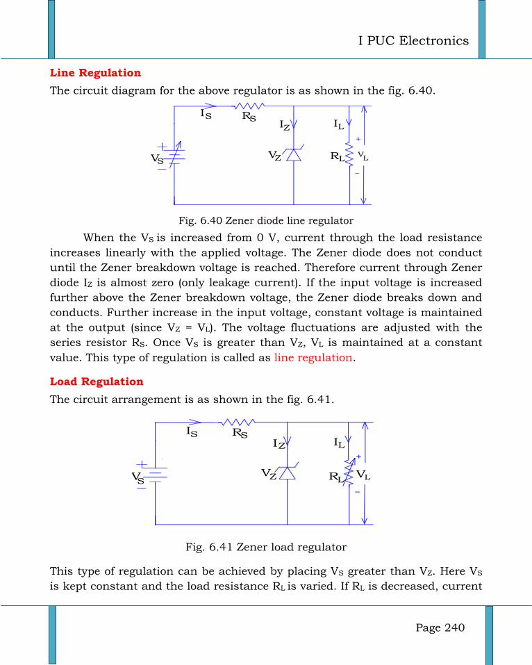
I PUC Electronics
Page 240
Line Regulation
The circuit diagram for the above regulator is as shown in the fig. 6.40.
VSVLRL
RS
VZ
ISIZ IL
Fig. 6.40 Zener diode line regulator
When the VS is increased from 0 V, current through the load resistance
increases linearly with the applied voltage. The Zener diode does not conduct
until the Zener breakdown voltage is reached. Therefore current through Zener
diode IZ is almost zero (only leakage current). If the input voltage is increased
further above the Zener breakdown voltage, the Zener diode breaks down and
conducts. Further increase in the input voltage, constant voltage is maintained
at the output (since VZ = VL). The voltage fluctuations are adjusted with the
series resistor RS. Once VS is greater than VZ, VL is maintained at a constant
value. This type of regulation is called as line regulation.
Load Regulation
The circuit arrangement is as shown in the fig. 6.41.
VS
VLRL
RS
VZ
ISIZ IL
Fig. 6.41 Zener load regulator
This type of regulation can be achieved by placing VS greater than VZ. Here VS
is kept constant and the load resistance RL is varied. If RL is decreased, current
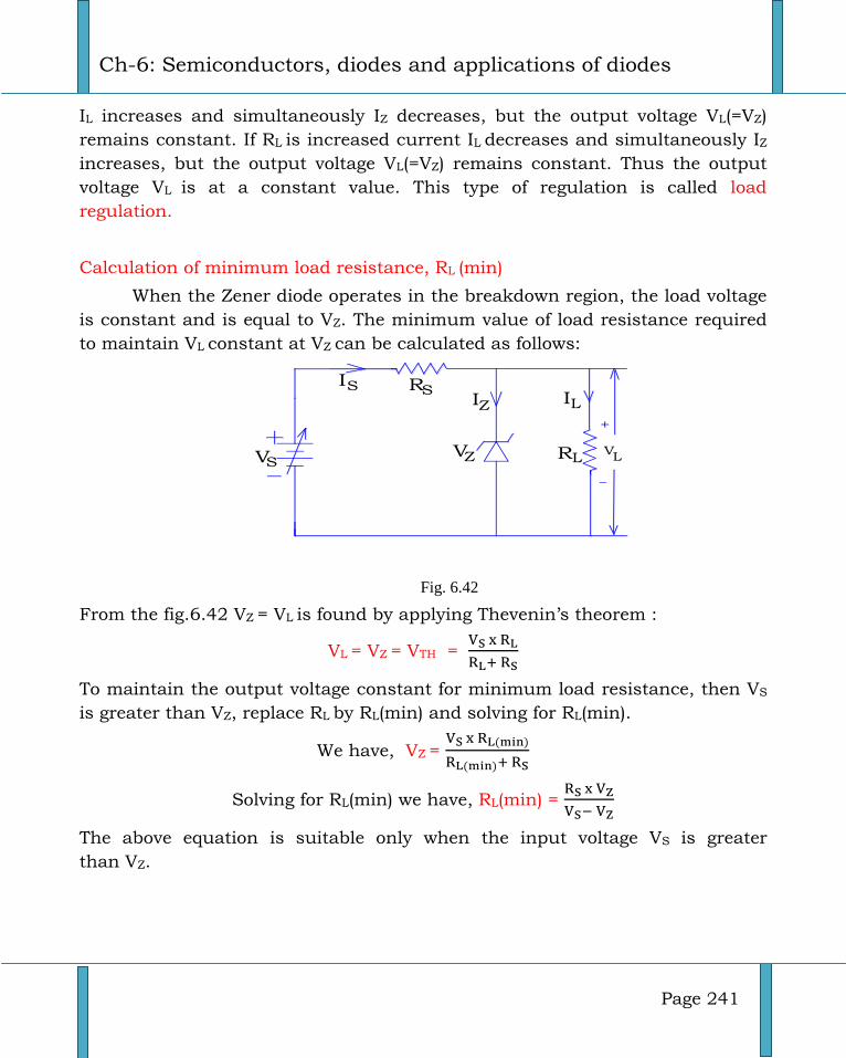
Ch-6: Semiconductors, diodes and applications of diodes
Page 241
IL increases and simultaneously IZ decreases, but the output voltage VL(=VZ)
remains constant. If RL is increased current IL decreases and simultaneously IZ
increases, but the output voltage VL(=VZ) remains constant. Thus the output
voltage VL is at a constant value. This type of regulation is called load
regulation.
Calculation of minimum load resistance, RL (min)
When the Zener diode operates in the breakdown region, the load voltage
is constant and is equal to VZ. The minimum value of load resistance required
to maintain VL constant at VZ can be calculated as follows:
VSVLRL
RS
VZ
ISIZ IL
Fig. 6.42
From the fig.6.42 VZ = VL is found by applying Thevenin’s theorem :
VL = VZ = VTH =
To maintain the output voltage constant for minimum load resistance, then VS
is greater than VZ, replace RL by RL(min) and solving for RL(min).
We have, VZ =
Solving for RL(min) we have, RL(min) =
The above equation is suitable only when the input voltage VS is greater
than VZ.
I PUC Electronics
Page 242
Optimum value of current limiting resistor
The value of RS must be properly selected to fulfill the following
requirements:
When the input voltage is minimum and the load current is maximum,
sufficient current must be supplied to keep the Zener diode within its
regulating region. The optimum value of RS can be found by using the following
equations:
IZ (max) =
IZ (min) =
Minimum value of RS makes the current flow in the Zener diode
maximum and vice versa,
Therefore, RS(min) =
RS(max) =
Hence the value of RS should be so chosen that RS(min) < RS < RS(max).
Percentage regulation
Regulation is expressed as a percentage. It is a figure of merit used to
specify the performance of a voltage regulator.
Line regulation
It is defined as a change in the output voltage (∆VL) for a given change in
the input voltage (∆VS) expressed as a percentage. i.e.,
Percentage of line regulation =
x 100%
Load regulation
It is defined as a change in the output voltage over a certain range of
load current values, usually from minimum current (no load) to maximum
current (full load). It is also expressed as a percentage.
Percentage of load regulation =
x 100%
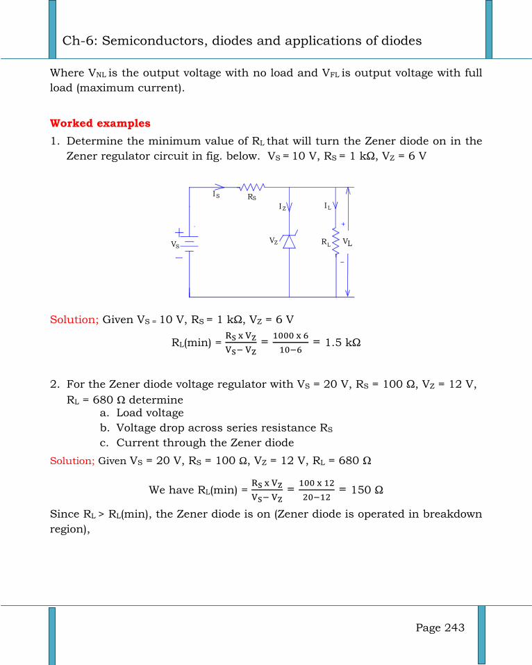
Ch-6: Semiconductors, diodes and applications of diodes
Page 243
Where VNL is the output voltage with no load and VFL is output voltage with full
load (maximum current).
Worked examples
1. Determine the minimum value of RL that will turn the Zener diode on in the
Zener regulator circuit in fig. below. VS = 10 V, RS = 1 kΩ, VZ = 6 V
VSVLRL
RS
VZ
IS
IZ IL
Solution; Given VS = 10 V, RS = 1 kΩ, VZ = 6 V
RL(min) =
=
= 1.5 kΩ
2. For the Zener diode voltage regulator with VS = 20 V, RS = 100 Ω, VZ = 12 V,
RL = 680 Ω determine a. Load voltage
b. Voltage drop across series resistance RS
c. Current through the Zener diode
Solution; Given VS = 20 V, RS = 100 Ω, VZ = 12 V, RL = 680 Ω
We have RL(min) =
=
= 150 Ω
Since RL > RL(min), the Zener diode is on (Zener diode is operated in breakdown
region),
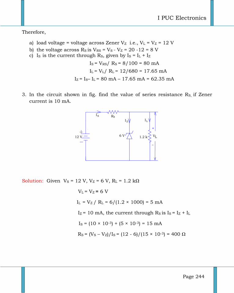
I PUC Electronics
Page 244
Therefore,
a) load voltage = voltage across Zener VZ i.e., VL = VZ = 12 V
b) the voltage across RS is VRS = VS - VZ = 20 -12 = 8 V c) IS is the current through RS, given by IS = IL + IZ
IS = VRS/ RS = 8/100 = 80 mA
IL = VL/ RL = 12/680 = 17.65 mA
IZ = IS– IL = 80 mA – 17.65 mA = 62.35 mA
3. In the circuit shown in fig. find the value of series resistance RS, if Zener
current is 10 mA.
12 V VL1.2 k
RS
6 V
IS
IZ IL
Solution: Given VS = 12 V, VZ = 6 V, RL = 1.2 kΩ
VL = VZ = 6 V
IL = VZ / RL = 6/(1.2 × 1000) = 5 mA
IZ = 10 mA, the current through RS is IS = IZ + IL
IS = (10 × 10-3) + (5 × 10⁻³) = 15 mA
RS = (VS – VZ)/IS = (12 - 6)/(15 × 10-3) = 400 Ω
Ch-6: Semiconductors, diodes and applications of diodes
Page 245
Design of a rectifier for the given DC voltage
Do you know how to design a rectifier for your radio or type-recorder ?
To design a rectifier for electronic equipment like radio, type-recorder etc,
it is necessary to know the voltage and current (power) rating of the equipment.
Once voltage and current ratings are known it is easy to design rectifier for any
equipment. For a given application transformer winding with suitable voltage
and current ratings must be selected. Transformers are always rated with rms
voltage and rms current specifications. Bridge rectifiers are commonly used in
power supplies.
We know that for bridge rectifier
Vdc =
=
√
……..(1)
Therefore Vrms =
√ ……..(2)
For example to get Vdc = 14 V from eqn (2) we get Vrms = 15.55 V.
Therefore choose the transformer with a secondary voltage to 16 V or use 15 V
which is available in market.
The current rating of the transformer is chosen depending on the current we
draw from the transformer (Idc). For the bridge rectifier
We have Idc =
=
√
……(3)
Therefore Irms =
√ …....(4)
For example to get Idc = 450 mA from eqn (4) we get Irms = 500 mA .
Select the transformer of input; 0 - 230 V and output 0 - 15 V/500 mA to get
DC of 14 V and 450 mA. Using design equation (2) select the transformer
secondary voltage Vrms for a given dc voltage Vdc and using the equation (4)
select the transformer secondary current Irms for a given Idc.
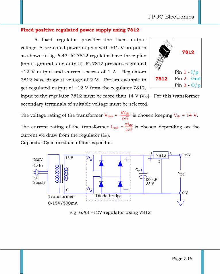
I PUC Electronics
Page 246
Fixed positive regulated power supply using 7812
A fixed regulator provides the fixed output
voltage. A regulated power supply with +12 V output is
as shown in fig. 6.43. IC 7812 regulator have three pins
(input, ground, and output). IC 7812 provides regulated
+12 V output and current excess of 1 A. Regulators
7812 have dropout voltage of 2 V. For an example to
get regulated output of +12 V from the regulator 7812,
input to the regulator 7812 must be more than 14 V (Vdc). For this transformer
secondary terminals of suitable voltage must be selected.
The voltage rating of the transformer Vrms =
√ is chosen keeping Vdc = 14 V.
The current rating of the transformer Irms =
√ is chosen depending on the
current we draw from the regulator (Idc).
Capacitor CF is used as a filter capacitor.
Transformer
0-15V/500mA
1000 µ35 V
230V
50 Hz
ACSupply
15 V
0
78121
2
3 +12V
0 V
CF
Diode bridge
VDC
Fig. 6.43 +12V regulator using 7812
7812
7812
Pin 1 - I/p
Pin 2 - Gnd
Pin 3 - O/p
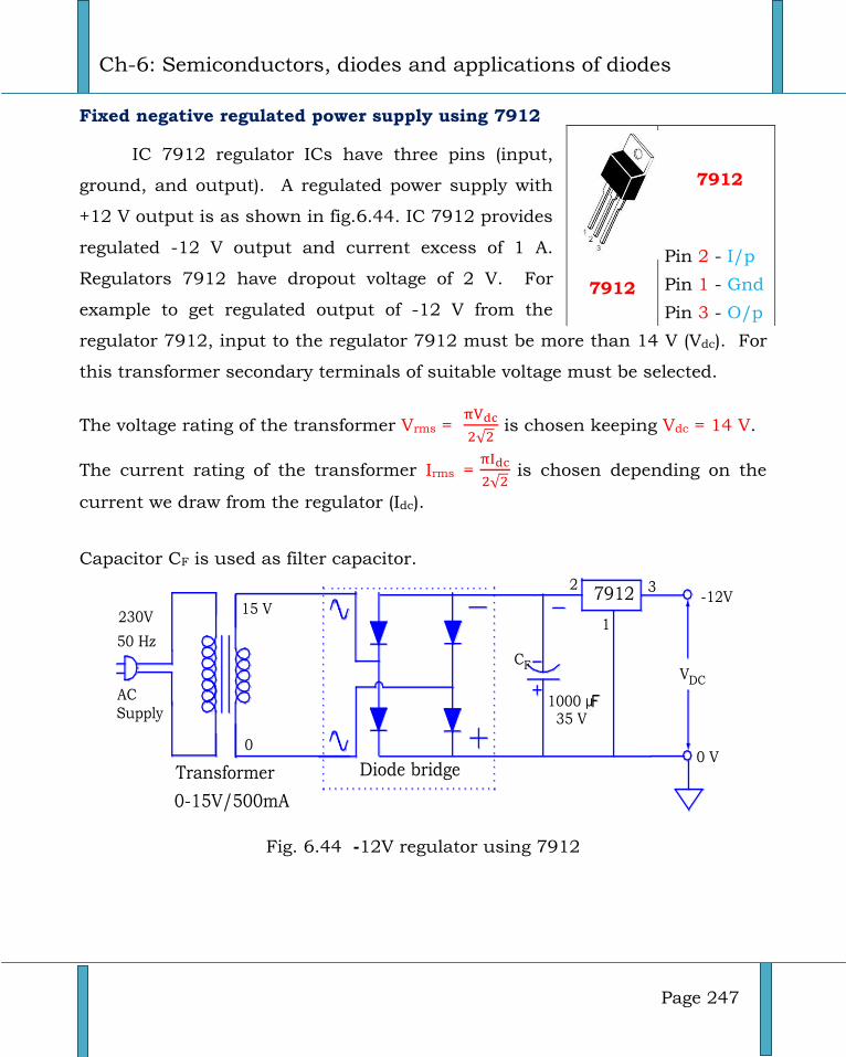
Ch-6: Semiconductors, diodes and applications of diodes
Page 247
Fixed negative regulated power supply using 7912
IC 7912 regulator ICs have three pins (input,
ground, and output). A regulated power supply with
+12 V output is as shown in fig.6.44. IC 7912 provides
regulated -12 V output and current excess of 1 A.
Regulators 7912 have dropout voltage of 2 V. For
example to get regulated output of -12 V from the
regulator 7912, input to the regulator 7912 must be more than 14 V (Vdc). For
this transformer secondary terminals of suitable voltage must be selected.
The voltage rating of the transformer Vrms =
√ is chosen keeping Vdc = 14 V.
The current rating of the transformer Irms =
√ is chosen depending on the
current we draw from the regulator (Idc).
Capacitor CF is used as filter capacitor.
Transformer
0-15V/500mA
1000 µ35 V
230V
50 Hz
ACSupply
15 V
0
79122
1
3 -12V
0 V
CF
Diode bridge
VDC
Fig. 6.44 -12V regulator using 7912
7912
7912
Pin 2 - I/p
Pin 1 - Gnd
Pin 3 - O/p
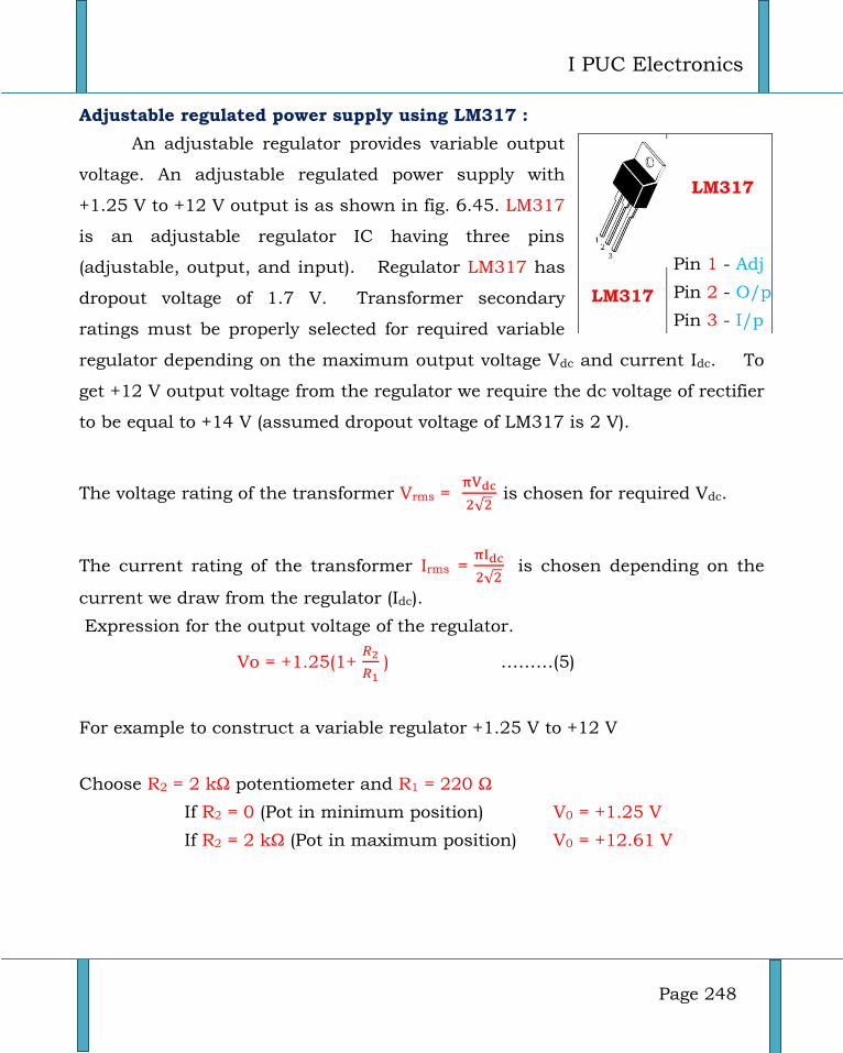
I PUC Electronics
Page 248
Adjustable regulated power supply using LM317 :
An adjustable regulator provides variable output
voltage. An adjustable regulated power supply with
+1.25 V to +12 V output is as shown in fig. 6.45. LM317
is an adjustable regulator IC having three pins
(adjustable, output, and input). Regulator LM317 has
dropout voltage of 1.7 V. Transformer secondary
ratings must be properly selected for required variable
regulator depending on the maximum output voltage Vdc and current Idc. To
get +12 V output voltage from the regulator we require the dc voltage of rectifier
to be equal to +14 V (assumed dropout voltage of LM317 is 2 V).
The voltage rating of the transformer Vrms =
√ is chosen for required Vdc.
The current rating of the transformer Irms =
√ is chosen depending on the
current we draw from the regulator (Idc).
Expression for the output voltage of the regulator.
Vo = +1.25(1+
) ………(5)
For example to construct a variable regulator +1.25 V to +12 V
Choose R2 = 2 kΩ potentiometer and R1 = 220 Ω
If R2 = 0 (Pot in minimum position) V0 = +1.25 V
If R2 = 2 kΩ (Pot in maximum position) V0 = +12.61 V
LM317
LM317
Pin 1 - Adj
Pin 2 - O/p
Pin 3 - I/p
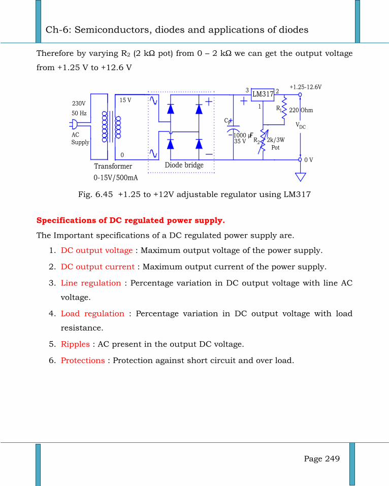
Ch-6: Semiconductors, diodes and applications of diodes
Page 249
Therefore by varying R2 (2 kΩ pot) from 0 – 2 kΩ we can get the output voltage
from +1.25 V to +12.6 V
Transformer
0-15V/500mA
1000 µ35 V
230V
50 Hz
ACSupply
15 V
0
LM3173
1
2
0 V
CF
Diode bridge
VDC
+1.25-12.6V
Pot
2k/3W
R1
R2
220 Ohm
Fig. 6.45 +1.25 to +12V adjustable regulator using LM317
Specifications of DC regulated power supply.
The Important specifications of a DC regulated power supply are.
1. DC output voltage : Maximum output voltage of the power supply.
2. DC output current : Maximum output current of the power supply.
3. Line regulation : Percentage variation in DC output voltage with line AC
voltage.
4. Load regulation : Percentage variation in DC output voltage with load
resistance.
5. Ripples : AC present in the output DC voltage.
6. Protections : Protection against short circuit and over load.
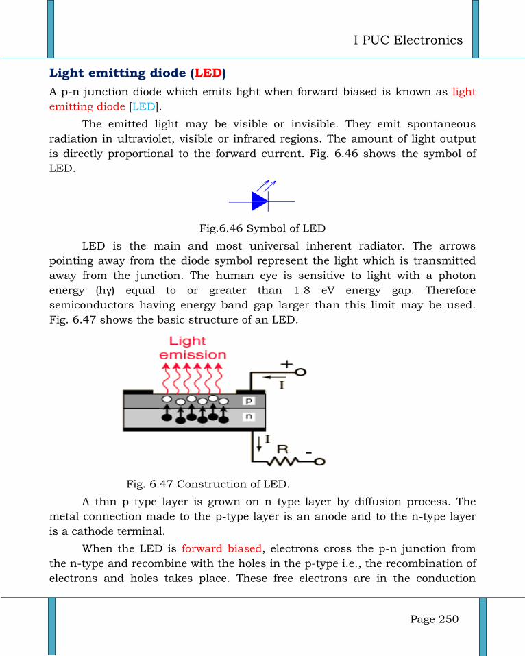
I PUC Electronics
Page 250
Light emitting diode (LED)
A p-n junction diode which emits light when forward biased is known as light
emitting diode [LED].
The emitted light may be visible or invisible. They emit spontaneous
radiation in ultraviolet, visible or infrared regions. The amount of light output
is directly proportional to the forward current. Fig. 6.46 shows the symbol of
LED.
Fig.6.46 Symbol of LED
LED is the main and most universal inherent radiator. The arrows
pointing away from the diode symbol represent the light which is transmitted
away from the junction. The human eye is sensitive to light with a photon
energy (hγ) equal to or greater than 1.8 eV energy gap. Therefore
semiconductors having energy band gap larger than this limit may be used.
Fig. 6.47 shows the basic structure of an LED.
Fig. 6.47 Construction of LED.
A thin p type layer is grown on n type layer by diffusion process. The
metal connection made to the p-type layer is an anode and to the n-type layer
is a cathode terminal.
When the LED is forward biased, electrons cross the p-n junction from
the n-type and recombine with the holes in the p-type i.e., the recombination of
electrons and holes takes place. These free electrons are in the conduction
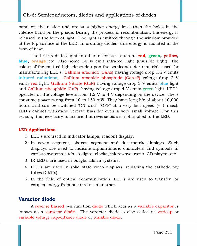
Ch-6: Semiconductors, diodes and applications of diodes
Page 251
band on the n side and are at a higher energy level than the holes in the
valence band on the p side. During the process of recombination, the energy is
released in the form of light. The light is emitted through the window provided
at the top surface of the LED. In ordinary diodes, this energy is radiated in the
form of heat.
The LED radiates light in different colours such as red, green, yellow,
blue, orange etc. Also some LEDs emit infrared light (invisible light). The
colour of the emitted light depends upon the semiconductor materials used for
manufacturing LED’s. Gallium arsenide (GaAs) having voltage drop 1.6 V emits
infrared radiations, Gallium arsenide phosphide (GaAsP) voltage drop 2 V
emits red light, Gallium Nitrate (GaN) having voltage drop 3 V emits blue light
and Gallium phosphide (GaP) having voltage drop 4 V emits green light. LED’s
operates at the voltage levels from 1.2 V to 4 V depending on the device. These
consume power rating from 10 to 150 mW. They have long life of about 10,000
hours and can be switched ‘ON’ and ‘OFF’ at a very fast speed (≈ 1 nsec).
LED’s cannot withstand reverse bias for even a very small voltage. For this
reason, it is necessary to assure that reverse bias is not applied to the LED.
LED Applications
1. LED’s are used in indicator lamps, readout display.
2. In seven segment, sixteen segment and dot matrix displays. Such
displays are used to indicate alphanumeric characters and symbols in
various systems such as digital clocks, microwave ovens, CD players etc.
3. IR LED’s are used in burglar alarm systems.
4. LED’s are used in solid state video displays, replacing the cathode ray
tubes (CRT’s)
5. In the field of optical communication, LED’s are used to transfer (or
couple) energy from one circuit to another.
Varactor diode
A reverse biased p-n junction diode which acts as a variable capacitor is
known as a varactor diode. The varactor diode is also called as varicap or
variable voltage capacitance diode or tunable diode.
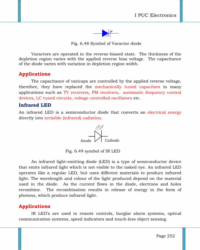
I PUC Electronics
Page 252
Fig. 6.48 Symbol of Varactor diode
Varactors are operated in the reverse-biased state. The thickness of the depletion region varies with the applied reverse bias voltage. The capacitance of the diode varies with variation in depletion region width.
Applications
The capacitance of varicaps are controlled by the applied reverse voltage,
therefore, they have replaced the mechanically tuned capacitors in many
applications such as TV receivers, FM receivers, automatic frequency control
devices, LC tuned circuits, voltage controlled oscillators etc.
Infrared LED
An infrared LED is a semiconductor diode that converts an electrical energy
directly into invisible (infrared) radiation.
Anode Cathode
Fig. 6.49 symbol of IR LED
An infrared light-emitting diode (LED) is a type of semiconductor device
that emits infrared light which is not visible to the naked eye. An infrared LED
operates like a regular LED, but uses different materials to produce infrared
light. The wavelength and colour of the light produced depend on the material
used in the diode. As the current flows in the diode, electrons and holes
recombine. The recombination results in release of energy in the form of
photons, which produce infrared light.
Applications
IR LED’s are used in remote controls, burglar alarm systems, optical
communication systems, speed indicators and touch-less object sensing.
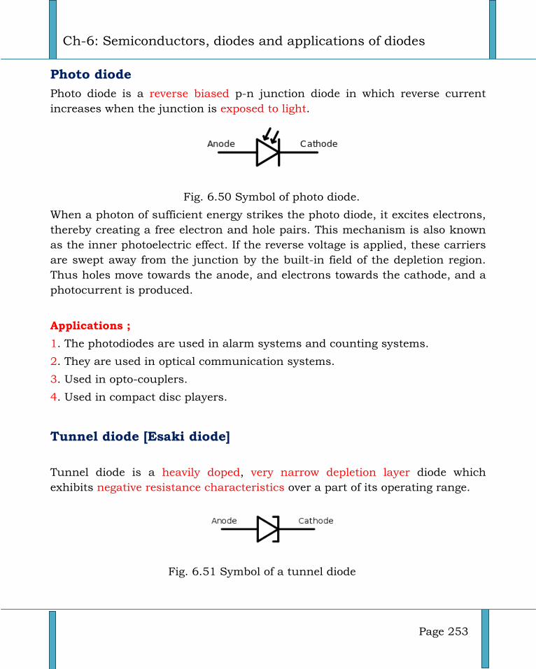
Ch-6: Semiconductors, diodes and applications of diodes
Page 253
Photo diode
Photo diode is a reverse biased p-n junction diode in which reverse current
increases when the junction is exposed to light.
Fig. 6.50 Symbol of photo diode.
When a photon of sufficient energy strikes the photo diode, it excites electrons,
thereby creating a free electron and hole pairs. This mechanism is also known
as the inner photoelectric effect. If the reverse voltage is applied, these carriers
are swept away from the junction by the built-in field of the depletion region.
Thus holes move towards the anode, and electrons towards the cathode, and a
photocurrent is produced.
Applications ;
1. The photodiodes are used in alarm systems and counting systems.
2. They are used in optical communication systems.
3. Used in opto-couplers.
4. Used in compact disc players.
Tunnel diode [Esaki diode]
Tunnel diode is a heavily doped, very narrow depletion layer diode which
exhibits negative resistance characteristics over a part of its operating range.
Fig. 6.51 Symbol of a tunnel diode
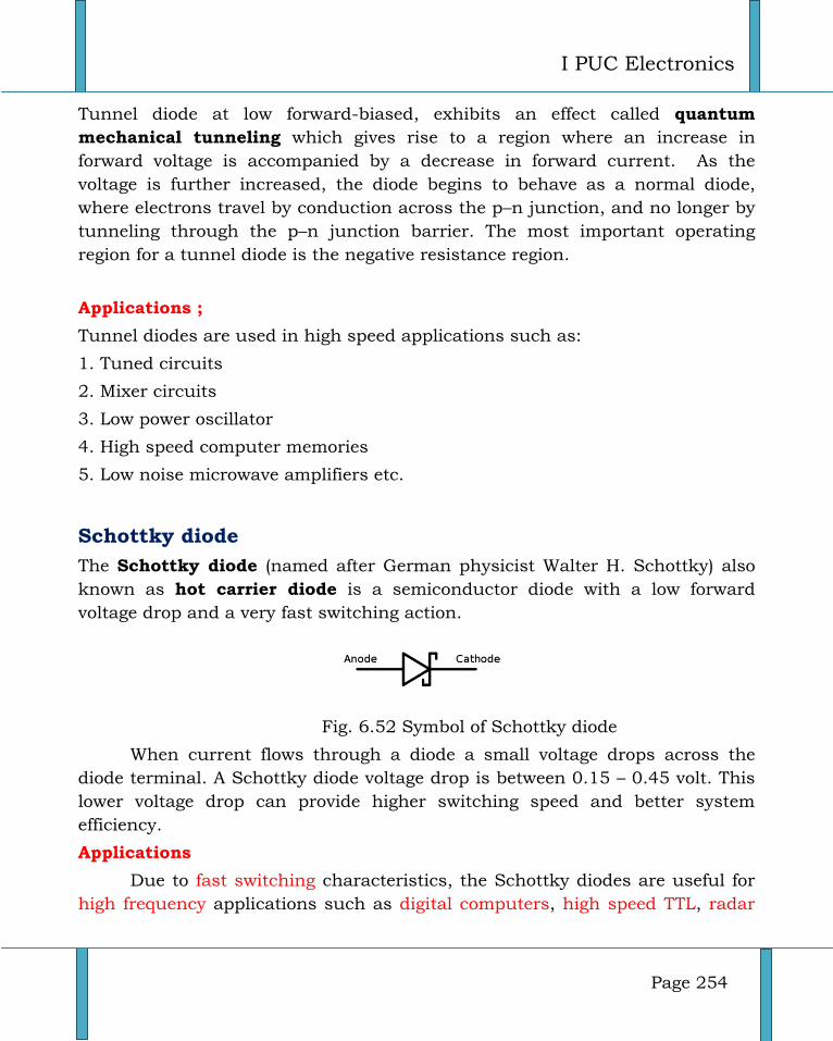
I PUC Electronics
Page 254
Tunnel diode at low forward-biased, exhibits an effect called quantum
mechanical tunneling which gives rise to a region where an increase in
forward voltage is accompanied by a decrease in forward current. As the
voltage is further increased, the diode begins to behave as a normal diode,
where electrons travel by conduction across the p–n junction, and no longer by
tunneling through the p–n junction barrier. The most important operating
region for a tunnel diode is the negative resistance region.
Applications ;
Tunnel diodes are used in high speed applications such as:
1. Tuned circuits
2. Mixer circuits
3. Low power oscillator
4. High speed computer memories
5. Low noise microwave amplifiers etc.
Schottky diode
The Schottky diode (named after German physicist Walter H. Schottky) also
known as hot carrier diode is a semiconductor diode with a low forward
voltage drop and a very fast switching action.
Fig. 6.52 Symbol of Schottky diode
When current flows through a diode a small voltage drops across the
diode terminal. A Schottky diode voltage drop is between 0.15 – 0.45 volt. This
lower voltage drop can provide higher switching speed and better system
efficiency.
Applications
Due to fast switching characteristics, the Schottky diodes are useful for
high frequency applications such as digital computers, high speed TTL, radar
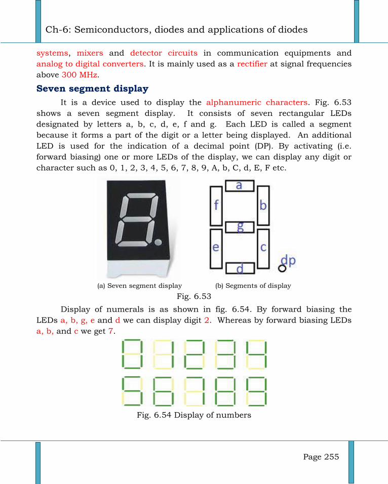
Ch-6: Semiconductors, diodes and applications of diodes
Page 255
systems, mixers and detector circuits in communication equipments and
analog to digital converters. It is mainly used as a rectifier at signal frequencies
above 300 MHz.
Seven segment display
It is a device used to display the alphanumeric characters. Fig. 6.53
shows a seven segment display. It consists of seven rectangular LEDs
designated by letters a, b, c, d, e, f and g. Each LED is called a segment
because it forms a part of the digit or a letter being displayed. An additional
LED is used for the indication of a decimal point (DP). By activating (i.e.
forward biasing) one or more LEDs of the display, we can display any digit or
character such as 0, 1, 2, 3, 4, 5, 6, 7, 8, 9, A, b, C, d, E, F etc.
(a) Seven segment display (b) Segments of display
Fig. 6.53
Display of numerals is as shown in fig. 6.54. By forward biasing the
LEDs a, b, g, e and d we can display digit 2. Whereas by forward biasing LEDs
a, b, and c we get 7.
Fig. 6.54 Display of numbers
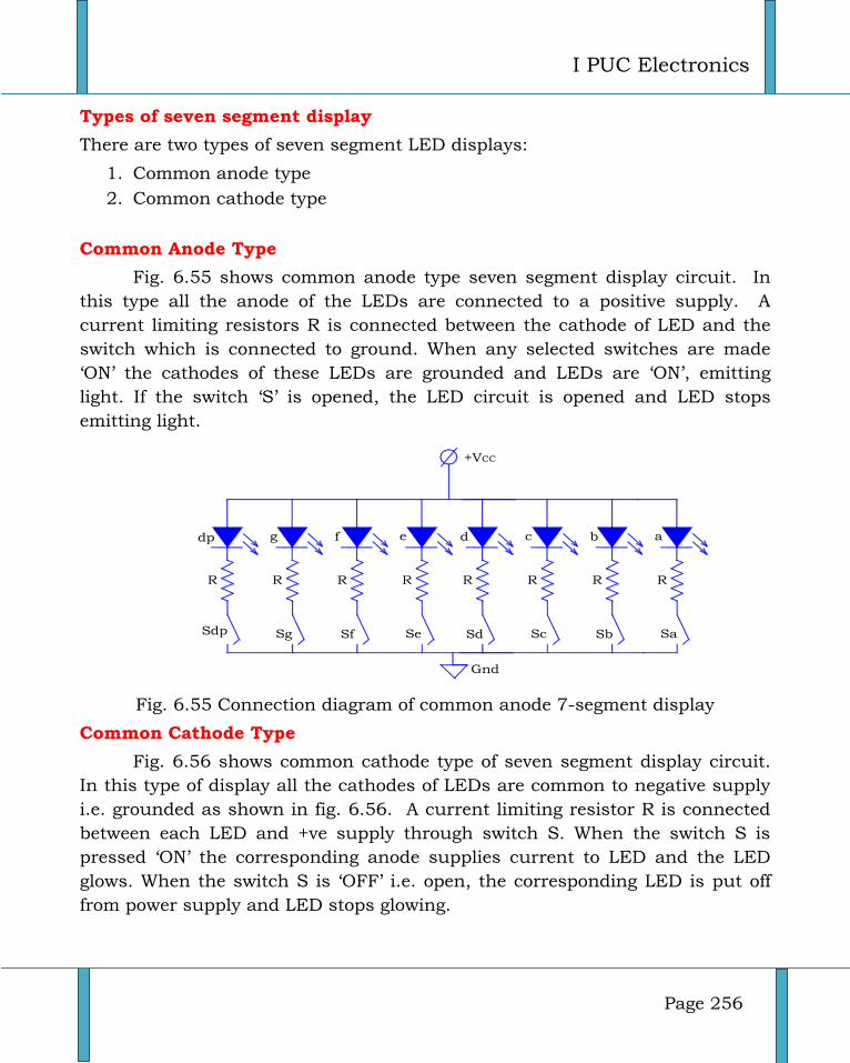
I PUC Electronics
Page 256
Types of seven segment display
There are two types of seven segment LED displays:
1. Common anode type
2. Common cathode type
Common Anode Type
Fig. 6.55 shows common anode type seven segment display circuit. In
this type all the anode of the LEDs are connected to a positive supply. A
current limiting resistors R is connected between the cathode of LED and the
switch which is connected to ground. When any selected switches are made
‘ON’ the cathodes of these LEDs are grounded and LEDs are ‘ON’, emitting
light. If the switch ‘S’ is opened, the LED circuit is opened and LED stops
emitting light.
f
R
Sf
e
R
Se
d
R
Sd
c
R
Sc
b
R
Sb
a
R
Sa
+VCC
Gnd
g
R
Sg
dp
R
Sdp
Fig. 6.55 Connection diagram of common anode 7-segment display
Common Cathode Type
Fig. 6.56 shows common cathode type of seven segment display circuit.
In this type of display all the cathodes of LEDs are common to negative supply
i.e. grounded as shown in fig. 6.56. A current limiting resistor R is connected
between each LED and +ve supply through switch S. When the switch S is
pressed ‘ON’ the corresponding anode supplies current to LED and the LED
glows. When the switch S is ‘OFF’ i.e. open, the corresponding LED is put off
from power supply and LED stops glowing.
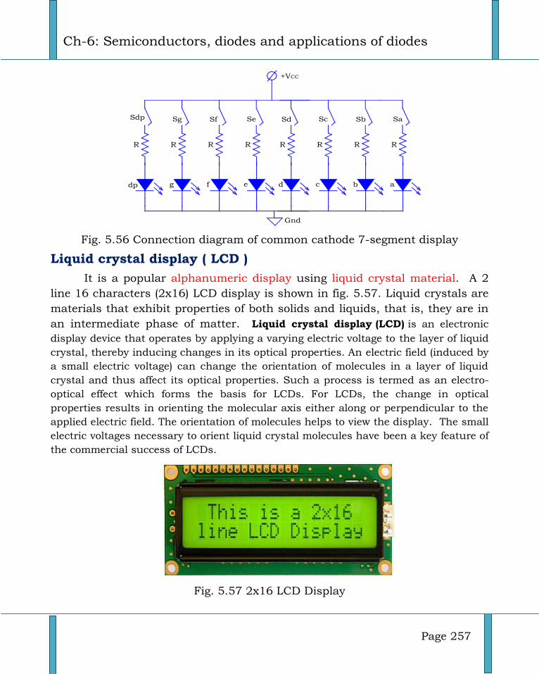
Ch-6: Semiconductors, diodes and applications of diodes
Page 257
dp g f e d c b a
+VCC
Gnd
R R R R R R R R
Sdp Sg Sf Se Sd Sc Sb Sa
Fig. 5.56 Connection diagram of common cathode 7-segment display
Liquid crystal display ( LCD )
It is a popular alphanumeric display using liquid crystal material. A 2
line 16 characters (2x16) LCD display is shown in fig. 5.57. Liquid crystals are
materials that exhibit properties of both solids and liquids, that is, they are in
an intermediate phase of matter. Liquid crystal display (LCD) is an electronic
display device that operates by applying a varying electric voltage to the layer of liquid
crystal, thereby inducing changes in its optical properties. An electric field (induced by
a small electric voltage) can change the orientation of molecules in a layer of liquid
crystal and thus affect its optical properties. Such a process is termed as an electro-
optical effect which forms the basis for LCDs. For LCDs, the change in optical
properties results in orienting the molecular axis either along or perpendicular to the
applied electric field. The orientation of molecules helps to view the display. The small
electric voltages necessary to orient liquid crystal molecules have been a key feature of
the commercial success of LCDs.
Fig. 5.57 2x16 LCD Display
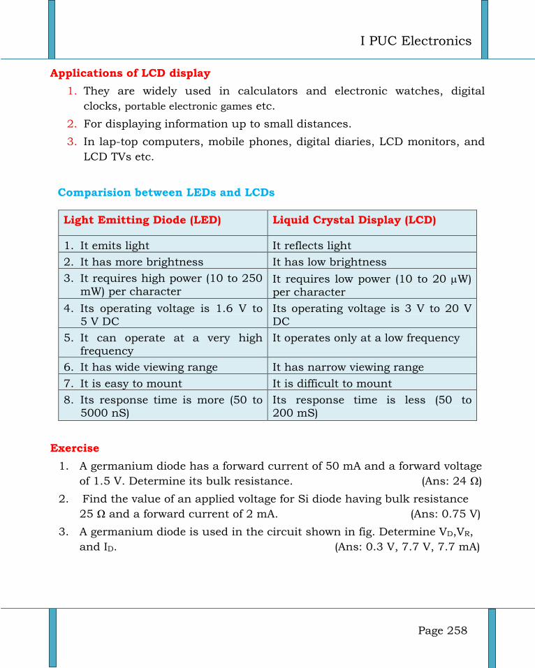
I PUC Electronics
Page 258
Applications of LCD display
1. They are widely used in calculators and electronic watches, digital
clocks, portable electronic games etc.
2. For displaying information up to small distances.
3. In lap-top computers, mobile phones, digital diaries, LCD monitors, and
LCD TVs etc.
Comparision between LEDs and LCDs
Light Emitting Diode (LED) Liquid Crystal Display (LCD)
1. It emits light It reflects light
2. It has more brightness It has low brightness
3. It requires high power (10 to 250
mW) per character It requires low power (10 to 20 W)
per character
4. Its operating voltage is 1.6 V to 5 V DC
Its operating voltage is 3 V to 20 V DC
5. It can operate at a very high frequency
It operates only at a low frequency
6. It has wide viewing range It has narrow viewing range
7. It is easy to mount It is difficult to mount
8. Its response time is more (50 to 5000 nS)
Its response time is less (50 to 200 mS)
Exercise
1. A germanium diode has a forward current of 50 mA and a forward voltage
of 1.5 V. Determine its bulk resistance. (Ans: 24 Ω)
2. Find the value of an applied voltage for Si diode having bulk resistance
25 Ω and a forward current of 2 mA. (Ans: 0.75 V)
3. A germanium diode is used in the circuit shown in fig. Determine VD,VR,
and ID. (Ans: 0.3 V, 7.7 V, 7.7 mA)
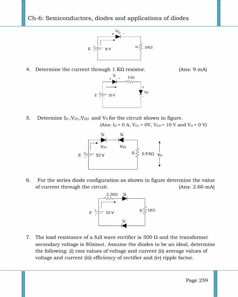
Ch-6: Semiconductors, diodes and applications of diodes
Page 259
4. Determine the current through 1 KΩ resistor. (Ans: 9 mA)
5. Determine ID ,VD1,VD2 and V0 for the circuit shown in figure.
(Ans: ID = 0 A, VD1 = 0V, VD2 = 10 V and VO = 0 V)
6. For the series diode configuration as shown in figure determine the value
of current through the circuit. (Ans: 2.60 mA)
7. The load resistance of a full wave rectifier is 500 Ω and the transformer
secondary voltage is 80sint. Assume the diodes to be an ideal, determine
the following: (i) rms values of voltage and current (ii) average values of
voltage and current (iii) efficiency of rectifier and (iv) ripple factor.
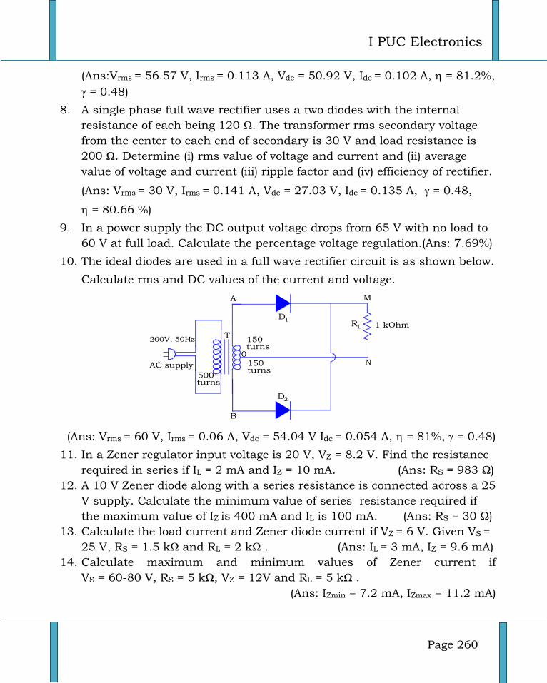
I PUC Electronics
Page 260
(Ans:Vrms = 56.57 V, Irms = 0.113 A, Vdc = 50.92 V, Idc = 0.102 A, = 81.2%,
= 0.48)
8. A single phase full wave rectifier uses a two diodes with the internal
resistance of each being 120 Ω. The transformer rms secondary voltage
from the center to each end of secondary is 30 V and load resistance is
200 Ω. Determine (i) rms value of voltage and current and (ii) average
value of voltage and current (iii) ripple factor and (iv) efficiency of rectifier.
(Ans: Vrms = 30 V, Irms = 0.141 A, Vdc = 27.03 V, Idc = 0.135 A, = 0.48,
= 80.66 %)
9. In a power supply the DC output voltage drops from 65 V with no load to
60 V at full load. Calculate the percentage voltage regulation.(Ans: 7.69%)
10. The ideal diodes are used in a full wave rectifier circuit is as shown below.
Calculate rms and DC values of the current and voltage.
AC supply
T
R L
A M
N
B
D 1
D 2
200V, 50Hz
500turns
150turns
150turns
0
1 kOhm
(Ans: Vrms = 60 V, Irms = 0.06 A, Vdc = 54.04 V Idc = 0.054 A, = 81%, = 0.48)
11. In a Zener regulator input voltage is 20 V, VZ = 8.2 V. Find the resistance
required in series if IL = 2 mA and IZ = 10 mA. (Ans: RS = 983 Ω)
12. A 10 V Zener diode along with a series resistance is connected across a 25
V supply. Calculate the minimum value of series resistance required if
the maximum value of IZ is 400 mA and IL is 100 mA. (Ans: RS = 30 Ω)
13. Calculate the load current and Zener diode current if VZ = 6 V. Given VS =
25 V, RS = 1.5 kΩ and RL = 2 kΩ . (Ans: IL = 3 mA, IZ = 9.6 mA)
14. Calculate maximum and minimum values of Zener current if
VS = 60-80 V, RS = 5 kΩ, VZ = 12V and RL = 5 kΩ .
(Ans: IZmin = 7.2 mA, IZmax = 11.2 mA)
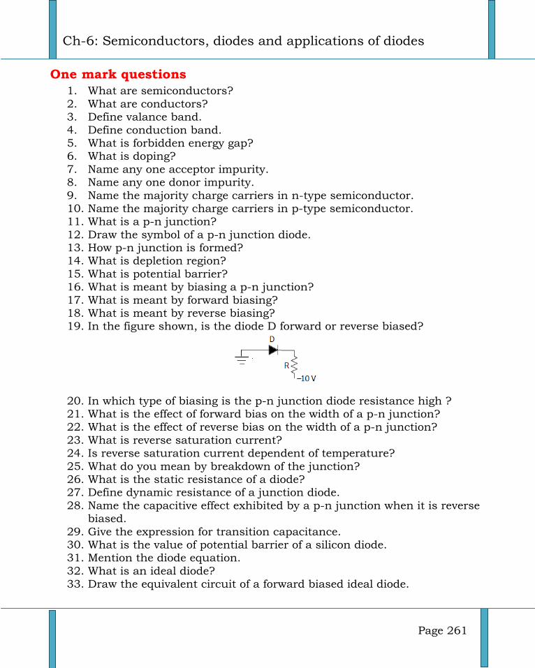
Ch-6: Semiconductors, diodes and applications of diodes
Page 261
One mark questions
1. What are semiconductors?
2. What are conductors? 3. Define valance band.
4. Define conduction band. 5. What is forbidden energy gap? 6. What is doping?
7. Name any one acceptor impurity. 8. Name any one donor impurity.
9. Name the majority charge carriers in n-type semiconductor. 10. Name the majority charge carriers in p-type semiconductor. 11. What is a p-n junction?
12. Draw the symbol of a p-n junction diode. 13. How p-n junction is formed? 14. What is depletion region?
15. What is potential barrier? 16. What is meant by biasing a p-n junction?
17. What is meant by forward biasing? 18. What is meant by reverse biasing? 19. In the figure shown, is the diode D forward or reverse biased?
20. In which type of biasing is the p-n junction diode resistance high ? 21. What is the effect of forward bias on the width of a p-n junction? 22. What is the effect of reverse bias on the width of a p-n junction?
23. What is reverse saturation current? 24. Is reverse saturation current dependent of temperature?
25. What do you mean by breakdown of the junction? 26. What is the static resistance of a diode? 27. Define dynamic resistance of a junction diode.
28. Name the capacitive effect exhibited by a p-n junction when it is reverse biased.
29. Give the expression for transition capacitance. 30. What is the value of potential barrier of a silicon diode. 31. Mention the diode equation.
32. What is an ideal diode? 33. Draw the equivalent circuit of a forward biased ideal diode.
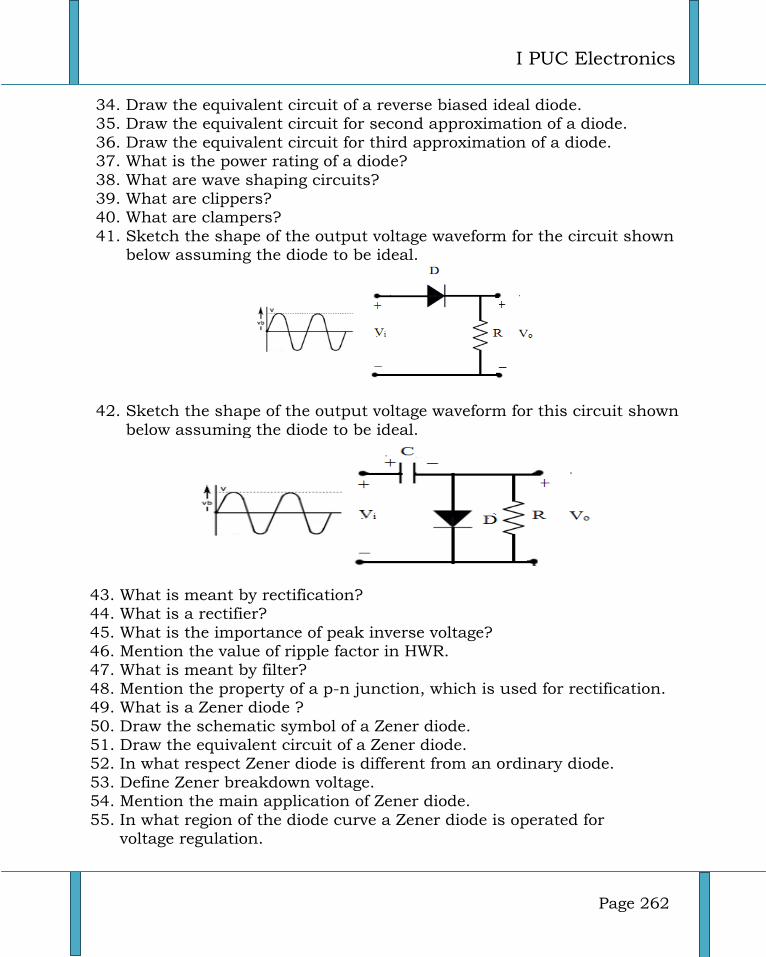
I PUC Electronics
Page 262
34. Draw the equivalent circuit of a reverse biased ideal diode. 35. Draw the equivalent circuit for second approximation of a diode.
36. Draw the equivalent circuit for third approximation of a diode. 37. What is the power rating of a diode?
38. What are wave shaping circuits? 39. What are clippers? 40. What are clampers?
41. Sketch the shape of the output voltage waveform for the circuit shown below assuming the diode to be ideal.
42. Sketch the shape of the output voltage waveform for this circuit shown
below assuming the diode to be ideal.
43. What is meant by rectification? 44. What is a rectifier?
45. What is the importance of peak inverse voltage? 46. Mention the value of ripple factor in HWR. 47. What is meant by filter?
48. Mention the property of a p-n junction, which is used for rectification. 49. What is a Zener diode ?
50. Draw the schematic symbol of a Zener diode. 51. Draw the equivalent circuit of a Zener diode. 52. In what respect Zener diode is different from an ordinary diode.
53. Define Zener breakdown voltage. 54. Mention the main application of Zener diode.
55. In what region of the diode curve a Zener diode is operated for voltage regulation.
Ch-6: Semiconductors, diodes and applications of diodes
Page 263
56. What is line regulation? 57. What is load regulation?
58. Name the active component used for voltage regulation. 59. Name the component used to construct +12 V fixed voltage regulator.
60. Name the component used to construct -12 V fixed voltage regulator. 61. Name the component used to construct adjustable voltage regulator. 62. What is LED?
63. Draw the schematic symbol of LED. 64. In what respect is LED different from an ordinary diode? 65. Under what bias is LED operated?
66. What happens to the light emission in LED as the forward current is increased?
67. What is a varactor diode? 68. Draw the symbol of a varactor diode. 69. Under what bias condition is a varactor diode operated?
70. Name any one application of a varactor diode. 71. What is an infrared LED?
72. Draw the symbol of an IR LED. 73. Name any one application of an IR LED. 74. What is a photodiode?
75. Draw the symbol of a photodiode. 76. Write the applications of a photodiode. 77. In what bias condition is a photodiode normally operated?
78. What is a tunnel diode? 79. Draw the symbol of a tunnel diode.
80. Name the applications of tunnel diode. 81. What is a Schottky diode? 82. Draw the symbol of a Schottky diode.
83. What is the range of voltage drop across the Schottky diode under forward biased condition?
84. Mention the applications of Schottky diode.
85. What is a seven segment LED display? 86. Mention the types of seven segment displays.
87. Mention any one application of a seven segment display. 88. What is a LCD? 89. Does LCD radiate its own light?
90. Mention any two important applications of LCD.
I PUC Electronics
Page 264
Two marks questions
1. Classify extrinsic semiconductor.
2. Draw the lattice structure of silicon.
3. Mention majority and minority charge carriers in n-type semiconductor. 4. Draw the crystalline structure of a p-type semiconductor. 5. What is meant by biasing?
6. Draw the circuit diagram of a forward biased p-n junction diode.
7. Draw the circuit diagram of a reverse biased p-n junction diode.
8. What is the origin of the reverse saturation current in a p-n junction?
9. Define static and dynamic resistance of a p-n junction diode.
10. What are the typical values of knee voltage for Ge and Si diodes.
11. Explain the phenomenon of diode reverse breakdown.
12. What do you mean by the transition capacitance of a diode?
13. A p-n junction diode is a non linear element. Explain.
14. Distinguish between Ge and Si diode.
15. Define ideal diode. Draw its V-I characteristics.
16. Explain the second approximation of a semiconductor diode.
17. Explain the third approximation of a semiconductor diode.
18. Explain the phenomenon of diode reverse breakdown.
19. Give any two examples for wave shaping circuits.
20. Mention any four applications of a diode.
21. What is meant by clipping? Mention any one application of clipping
circuit.
22. What is the difference between positive and negative clipper?
23. What is meant by clamping? Mention any one application of clamping
circuit.
24. Write the circuit of series positive clipper and show the input and output
waveforms.
25. Write the circuit of series negative clipper and show the input and output
waveforms.
26. Write the circuit of positive clamper and show the input and output
waveforms.
27. Write the circuit of negative clamper and show the input and output
waveforms.
Ch-6: Semiconductors, diodes and applications of diodes
Page 265
28. Mention the primary conditions of clamping circuits.
29. What is the difference between positive and negative clamper?
30. Mention any two comparisons of three rectifiers.
31. Define ripple factor and give its significance.
32. Draw the circuit diagram of a full wave rectifier indicating the input and
output wave forms.
33. How many diodes are used in a (i) Centre tapped full wave rectifier and
(ii) Bridge rectifier?
34. What is the maximum rectification efficiency of a full wave rectifier
and half wave rectifier?
35. Distinguish between full wave rectifier and half wave rectifier.
36. Distinguish between series inductor filter and shunt capacitor filter.
37. What is Zener break down?
38. Draw the VI Characteristics of Zener diode.
39. Explain the need of a voltage regulator circuit in a power supply.
40. Draw the circuit diagram of +12 V voltage regulator.
41. Draw the circuit diagram of an adjustable voltage regulator.
42. What is voltage regulation? Mention the types of voltage regulation.
43. State any two application of LED.
44. Draw the diagram of seven segment LED display.
45. Name any two elements used in the manufacture of LED.
Three/five marks questions
1. Classify solids based on energy band diagram.
2. Write the properties of semiconductor.
3. Briefly explain about the n-type semiconductor.
4. Briefly explain about the p-type semiconductor.
5. How is the depletion region formed in a p-n junction?
6. Explain the working of a p-n junction when it is forward biased.
7. Explain the working of a p-n junction when it is reverse biased.
8. Draw and explain the V-I characteristics of a p-n junction diode.
9. Explain an experiment to draw the forward and reverse characteristics of
a semiconductor diode.
10. Write a note on diode junction capacitance.
11. Write a note on diode specifications.
I PUC Electronics
Page 266
12. Write a note on diode approximations.
13. Explain the action of series positive clipper.
14. Explain the action of series negative clipper.
15. Explain the working of positive clamper.
16. Explain the working of negative clamper.
17. Describe the action of a diode as a half wave rectifier.
18. Explain the working of full wave centre tapped rectifier.
19. Explain the operation of bridge rectifier.
20. Explain the negative voltage rectifier.
21. Explain the working of a series inductor filter.
22. Explain the working of a shunt capacitor filter.
23. Mention any four comparisons of three rectifiers.
24. Explain the characteristics of a Zener diode.
25. Explain the working of a Zener diode as a voltage regulator.
26. Explain the regulated +12 V DC power supply.
27. Explain the regulated -12 V power supply.
28. Explain the working of LED.
29. Explain common anode type of seven segment display.
30. Compare LED display with LCD display.
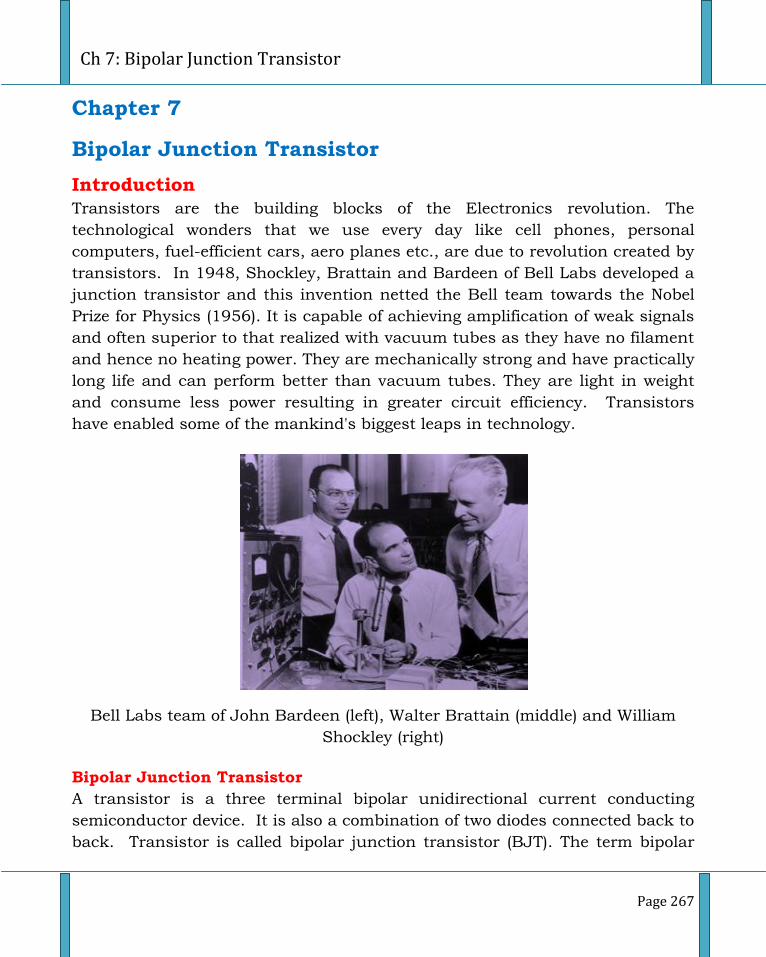
Ch 7: Bipolar Junction Transistor
Page 267
Chapter 7
Bipolar Junction Transistor
Introduction
Transistors are the building blocks of the Electronics revolution. The
technological wonders that we use every day like cell phones, personal
computers, fuel-efficient cars, aero planes etc., are due to revolution created by
transistors. In 1948, Shockley, Brattain and Bardeen of Bell Labs developed a
junction transistor and this invention netted the Bell team towards the Nobel
Prize for Physics (1956). It is capable of achieving amplification of weak signals
and often superior to that realized with vacuum tubes as they have no filament
and hence no heating power. They are mechanically strong and have practically
long life and can perform better than vacuum tubes. They are light in weight
and consume less power resulting in greater circuit efficiency. Transistors
have enabled some of the mankind's biggest leaps in technology.
Bell Labs team of John Bardeen (left), Walter Brattain (middle) and William
Shockley (right)
Bipolar Junction Transistor
A transistor is a three terminal bipolar unidirectional current conducting
semiconductor device. It is also a combination of two diodes connected back to
back. Transistor is called bipolar junction transistor (BJT). The term bipolar
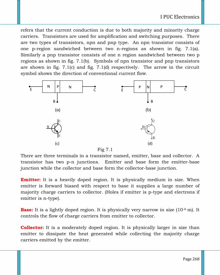
I PUC Electronics
Page 268
refers that the current conduction is due to both majority and minority charge
carriers. Transistors are used for amplification and switching purposes. There
are two types of transistors, npn and pnp type. An npn transistor consists of
one p-region sandwiched between two n-regions as shown in fig. 7.1(a).
Similarly a pnp transistor consists of one n region sandwiched between two p
regions as shown in fig. 7.1(b). Symbols of npn transistor and pnp transistors
are shown in fig. 7.1(c) and fig. 7.1(d) respectively. The arrow in the circuit
symbol shows the direction of conventional current flow.
(a) (b)
C
B
E (c) (d)
Fig 7.1
There are three terminals in a transistor named, emitter, base and collector. A
transistor has two p-n junctions. Emitter and base form the emitter-base
junction while the collector and base form the collector-base junction.
Emitter: It is a heavily doped region. It is physically medium in size. When
emitter is forward biased with respect to base it supplies a large number of
majority charge carriers to collector. (Holes if emitter is p-type and electrons if
emitter is n-type).
Base: It is a lightly doped region. It is physically very narrow in size (10-6 m). It
controls the flow of charge carriers from emitter to collector.
Collector: It is a moderately doped region. It is physically larger in size than
emitter to dissipate the heat generated while collecting the majority charge
carriers emitted by the emitter.
N P N
B
C E P N P
B
C E
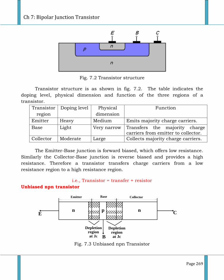
Ch 7: Bipolar Junction Transistor
Page 269
Fig. 7.2 Transistor structure
Transistor structure is as shown in fig. 7.2. The table indicates the
doping level, physical dimension and function of the three regions of a
transistor.
Transistor
region
Doping level Physical
dimension
Function
Emitter Heavy Medium Emits majority charge carriers.
Base Light Very narrow Transfers the majority charge carriers from emitter to collector.
Collector Moderate Large Collects majority charge carriers.
The Emitter-Base junction is forward biased, which offers low resistance.
Similarly the Collector-Base junction is reverse biased and provides a high
resistance. Therefore a transistor transfers charge carriers from a low
resistance region to a high resistance region.
i.e., Transistor = transfer + resistor
Unbiased npn transistor
Fig. 7.3 Unbiased npn Transistor
CE
B
Base CollectorEmitter
n p n
Depletionregion at JE
Depletionregion at Jc
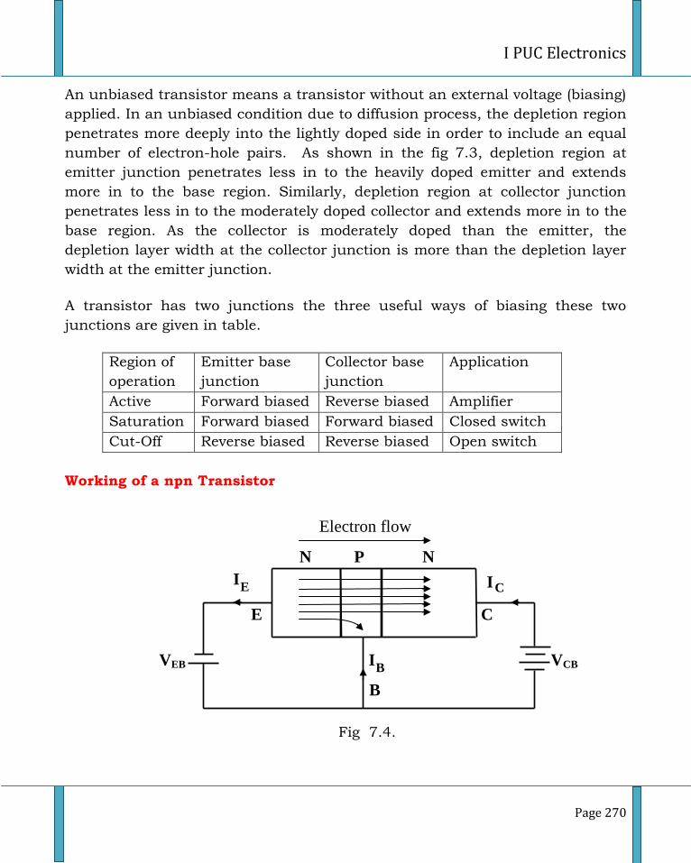
I PUC Electronics
Page 270
An unbiased transistor means a transistor without an external voltage (biasing)
applied. In an unbiased condition due to diffusion process, the depletion region
penetrates more deeply into the lightly doped side in order to include an equal
number of electron-hole pairs. As shown in the fig 7.3, depletion region at
emitter junction penetrates less in to the heavily doped emitter and extends
more in to the base region. Similarly, depletion region at collector junction
penetrates less in to the moderately doped collector and extends more in to the
base region. As the collector is moderately doped than the emitter, the
depletion layer width at the collector junction is more than the depletion layer
width at the emitter junction.
A transistor has two junctions the three useful ways of biasing these two
junctions are given in table.
Region of
operation
Emitter base
junction
Collector base
junction
Application
Active Forward biased Reverse biased Amplifier
Saturation Forward biased Forward biased Closed switch
Cut-Off Reverse biased Reverse biased Open switch
Working of a npn Transistor
Fig 7.4.
E
B
C
VEB VCB
P N N
Electron flow
I C I
E
I B
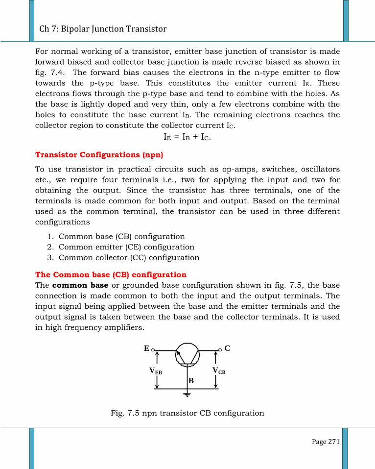
Ch 7: Bipolar Junction Transistor
Page 271
For normal working of a transistor, emitter base junction of transistor is made
forward biased and collector base junction is made reverse biased as shown in
fig. 7.4. The forward bias causes the electrons in the n-type emitter to flow
towards the p-type base. This constitutes the emitter current IE. These
electrons flows through the p-type base and tend to combine with the holes. As
the base is lightly doped and very thin, only a few electrons combine with the
holes to constitute the base current IB. The remaining electrons reaches the
collector region to constitute the collector current IC.
IE = IB + IC.
Transistor Configurations (npn)
To use transistor in practical circuits such as op-amps, switches, oscillators
etc., we require four terminals i.e., two for applying the input and two for
obtaining the output. Since the transistor has three terminals, one of the
terminals is made common for both input and output. Based on the terminal
used as the common terminal, the transistor can be used in three different
configurations
1. Common base (CB) configuration
2. Common emitter (CE) configuration
3. Common collector (CC) configuration
The Common base (CB) configuration
The common base or grounded base configuration shown in fig. 7.5, the base
connection is made common to both the input and the output terminals. The
input signal being applied between the base and the emitter terminals and the
output signal is taken between the base and the collector terminals. It is used
in high frequency amplifiers.
Fig. 7.5 npn transistor CB configuration
VEB VCB
C E
B
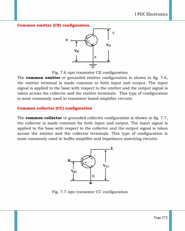
I PUC Electronics
Page 272
Common emitter (CE) configuration
Fig. 7.6 npn transistor CE configuration
The common emitter or grounded emitter configuration is shown in fig. 7.6,
the emitter terminal is made common to both input and output. The input
signal is applied to the base with respect to the emitter and the output signal is
taken across the collector and the emitter terminals. This type of configuration
is most commonly used in transistor based amplifier circuits.
Common collector (CC) configuration
The common collector or grounded collector configuration is shown in fig. 7.7,
the collector is made common for both input and output. The input signal is
applied to the base with respect to the collector and the output signal is taken
across the emitter and the collector terminals. This type of configuration is
most commonly used in buffer amplifier and impedance matching circuits.
Fig. 7.7 npn transistor CC configuration
P N
N
VEC
VBC
B
E
C
VBE
C
E
B P
N
N
VCE
Ch 7: Bipolar Junction Transistor
Page 273
DC current gain of the transistor
DC dc): dc is the ratio of collector current to the
emitter current in CB mode.
dc =
The value
DC Current gain in CE mode (βdc): βdc is the ratio of collector current to the
base current in CE mode.
βdc =
Relationship between and β in a transistor
We Know that IE = IB + IC ------ (1)
β =
Substitute equation (1) in the above equation
Divide both numerator and denominator by IB
β =
=
Similarly we get =
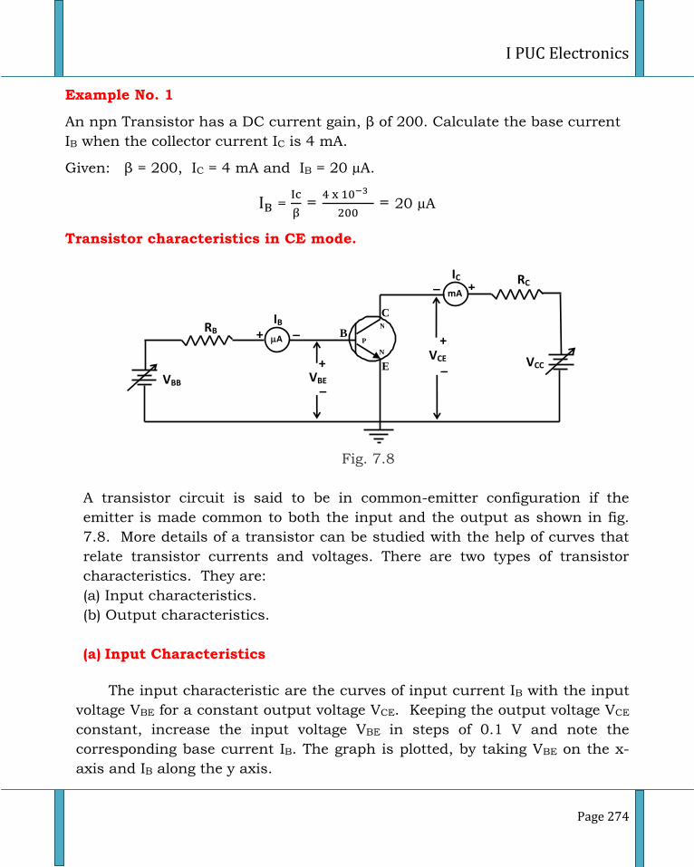
I PUC Electronics
Page 274
Example No. 1
An npn Transistor has a DC current gain, β of 200. Calculate the base current
IB when the collector current IC is 4 mA.
Given: β = 200, IC = 4 mA and IB = 20 µA.
=
=
= 20 µA
Transistor characteristics in CE mode.
Fig. 7.8
A transistor circuit is said to be in common-emitter configuration if the
emitter is made common to both the input and the output as shown in fig.
7.8. More details of a transistor can be studied with the help of curves that
relate transistor currents and voltages. There are two types of transistor
characteristics. They are:
(a) Input characteristics.
(b) Output characteristics.
(a) Input Characteristics
The input characteristic are the curves of input current IB with the input
voltage VBE for a constant output voltage VCE. Keeping the output voltage VCE
constant, increase the input voltage VBE in steps of 0.1 V and note the
corresponding base current IB. The graph is plotted, by taking VBE on the x-
axis and IB along the y axis.
IB +
+
A
VBE
RB C
E
B P
N
N
VBB
VCE +
VCC
RC mA
+ IC
_
_ _
_
_
_
_
_
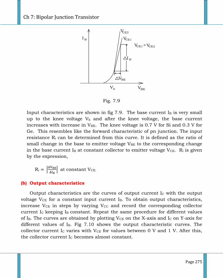
Ch 7: Bipolar Junction Transistor
Page 275
VCE1I B
VCE2
VBE
I B
VBE
V >CE1 VCE2
V k
Fig. 7.9
Input characteristics are shown in fig 7.9. The base current IB is very small
up to the knee voltage Vk and after the knee voltage, the base current
increases with increase in VBE. The knee voltage is 0.7 V for Si and 0.3 V for
Ge. This resembles like the forward characteristic of pn junction. The input
resistance Ri can be determined from this curve. It is defined as the ratio of
small change in the base to emitter voltage VBE to the corresponding change
in the base current IB at constant collector to emitter voltage VCE. Ri is given
by the expression,
Ri |
| at constant VCE.
(b) Output characteristics
Output characteristics are the curves of output current IC with the output
voltage VCE for a constant input current IB. To obtain output characteristics,
increase VCE in steps by varying VCC and record the corresponding collector
current IC keeping IB constant. Repeat the same procedure for different values
of IB. The curves are obtained by plotting VCE on the X-axis and IC on Y-axis for
different values of IB. Fig 7.10 shows the output characteristic curves. The
collector current IC varies with VCE for values between 0 V and 1 V. After this,
the collector current IC becomes almost constant.
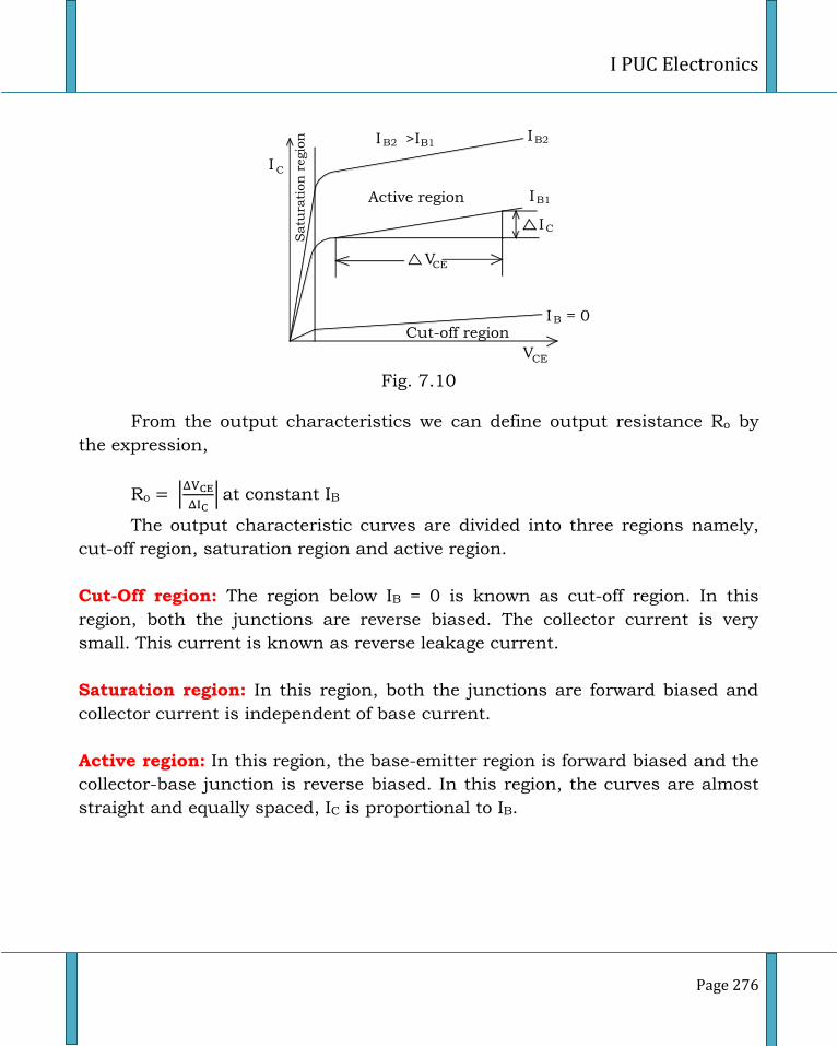
I PUC Electronics
Page 276
IB1
IB2I >IB2 B1
I C
VCE
IC
V CE
I = 0B
Cut-off region
Satu
rati
on
regio
n
Active region
Fig. 7.10
From the output characteristics we can define output resistance Ro by
the expression,
Ro |
| at constant IB
The output characteristic curves are divided into three regions namely,
cut-off region, saturation region and active region.
Cut-Off region: The region below IB = 0 is known as cut-off region. In this
region, both the junctions are reverse biased. The collector current is very
small. This current is known as reverse leakage current.
Saturation region: In this region, both the junctions are forward biased and
collector current is independent of base current.
Active region: In this region, the base-emitter region is forward biased and the
collector-base junction is reverse biased. In this region, the curves are almost
straight and equally spaced, IC is proportional to IB.
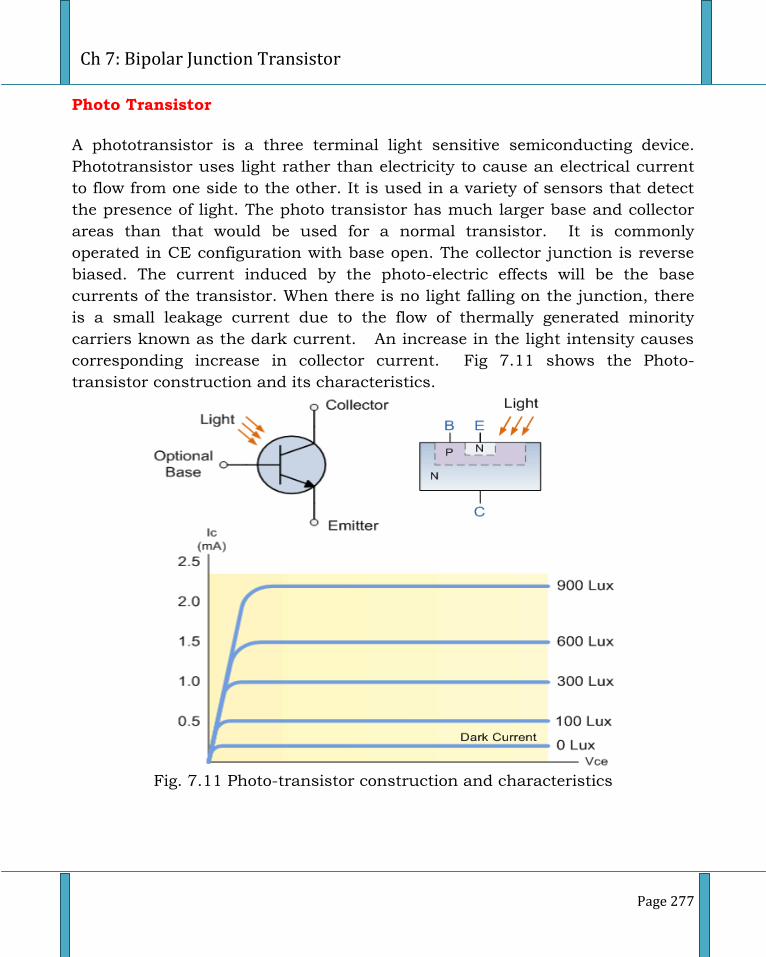
Ch 7: Bipolar Junction Transistor
Page 277
Photo Transistor
A phototransistor is a three terminal light sensitive semiconducting device.
Phototransistor uses light rather than electricity to cause an electrical current
to flow from one side to the other. It is used in a variety of sensors that detect
the presence of light. The photo transistor has much larger base and collector
areas than that would be used for a normal transistor. It is commonly
operated in CE configuration with base open. The collector junction is reverse
biased. The current induced by the photo-electric effects will be the base
currents of the transistor. When there is no light falling on the junction, there
is a small leakage current due to the flow of thermally generated minority
carriers known as the dark current. An increase in the light intensity causes
corresponding increase in collector current. Fig 7.11 shows the Photo-
transistor construction and its characteristics.
Fig. 7.11 Photo-transistor construction and characteristics
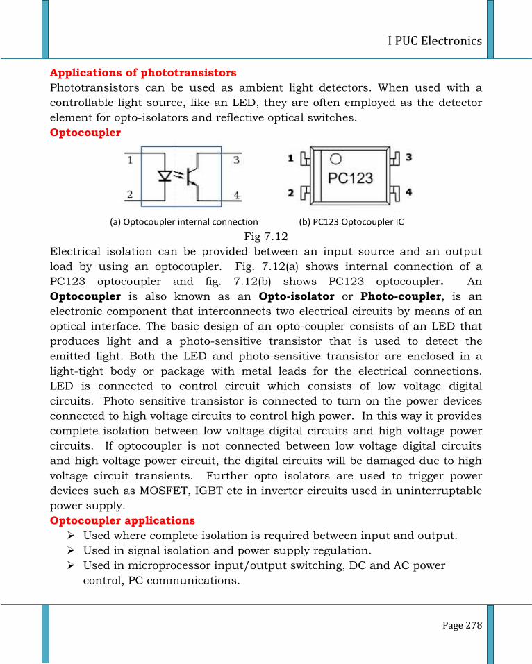
I PUC Electronics
Page 278
Applications of phototransistors
Phototransistors can be used as ambient light detectors. When used with a
controllable light source, like an LED, they are often employed as the detector
element for opto-isolators and reflective optical switches.
Optocoupler
(a) Optocoupler internal connection (b) PC123 Optocoupler IC
Fig 7.12
Electrical isolation can be provided between an input source and an output
load by using an optocoupler. Fig. 7.12(a) shows internal connection of a
PC123 optocoupler and fig. 7.12(b) shows PC123 optocoupler. An
Optocoupler is also known as an Opto-isolator or Photo-coupler, is an
electronic component that interconnects two electrical circuits by means of an
optical interface. The basic design of an opto-coupler consists of an LED that
produces light and a photo-sensitive transistor that is used to detect the
emitted light. Both the LED and photo-sensitive transistor are enclosed in a
light-tight body or package with metal leads for the electrical connections.
LED is connected to control circuit which consists of low voltage digital
circuits. Photo sensitive transistor is connected to turn on the power devices
connected to high voltage circuits to control high power. In this way it provides
complete isolation between low voltage digital circuits and high voltage power
circuits. If optocoupler is not connected between low voltage digital circuits
and high voltage power circuit, the digital circuits will be damaged due to high
voltage circuit transients. Further opto isolators are used to trigger power
devices such as MOSFET, IGBT etc in inverter circuits used in uninterruptable
power supply.
Optocoupler applications
Used where complete isolation is required between input and output.
Used in signal isolation and power supply regulation.
Used in microprocessor input/output switching, DC and AC power
control, PC communications.
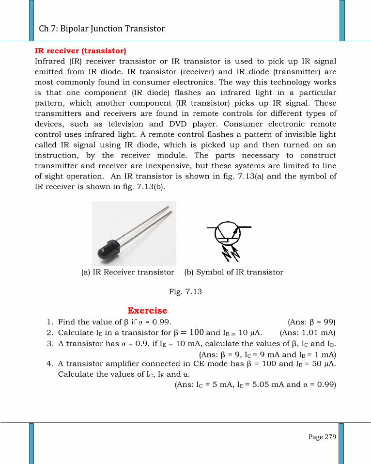
Ch 7: Bipolar Junction Transistor
Page 279
IR receiver (transistor)
Infrared (IR) receiver transistor or IR transistor is used to pick up IR signal
emitted from IR diode. IR transistor (receiver) and IR diode (transmitter) are
most commonly found in consumer electronics. The way this technology works
is that one component (IR diode) flashes an infrared light in a particular
pattern, which another component (IR transistor) picks up IR signal. These
transmitters and receivers are found in remote controls for different types of
devices, such as television and DVD player. Consumer electronic remote
control uses infrared light. A remote control flashes a pattern of invisible light
called IR signal using IR diode, which is picked up and then turned on an
instruction, by the receiver module. The parts necessary to construct
transmitter and receiver are inexpensive, but these systems are limited to line
of sight operation. An IR transistor is shown in fig. 7.13(a) and the symbol of
IR receiver is shown in fig. 7.13(b).
(a) IR Receiver transistor (b) Symbol of IR transistor
Fig. 7.13
Exercise
1. Find the value of β . (Ans: β = 99)
2. Calculate IE in a transistor for β and IB = 10 µA. (Ans: 1.01 mA)
3. A transistor has = 0.9, if IE = 10 mA, calculate the values of β, IC and IB.
(Ans: β = 9, IC = 9 mA and IB = 1 mA) 4. A transistor amplifier connected in CE mode has β = 100 and IB = 50 µA.
Calculate the values of IC, IE and .
(Ans: IC = 5 mA, IE = 5.05 mA and = 0.99)
I PUC Electronics
Page 280
One mark questions 1. What is a transistor?
2. Write one important application of a transistor. 3. What is an npn transistor?
4. Draw the symbol of a npn transistor. 5. Draw the symbol of a pnp transistor. 6. Why is transistor called transfer resistor device?
7. How many pn junctions a transistor has? 8. What is an unbiased transistor? 9. What is a biased transistor?
10. Mention the heavily doped region of a transistor. 11. Write the relation between the current components of a transistor.
12. What does an arrow in the circuit symbol of transistor indicate? 13. In which mode of operation the transistor can be used as an amplifier? 14. In which modes of operation the transistor can be used as a switch?
15. What is an opto-coupler?
Two mark question 1. Why is collector of transistor made larger and moderately doped? 2. Distinguish between dc and βdc.
3. Define dc and write its expression. 4. Define βdc and write its expression. 5. Distinguish between cut-off region and saturation region.
6. What is a phototransistor? Draw its symbol. 7. Write any two applications of phototransistors.
8. Mention lightly doped and the moderately doped regions of a transistor. 9. What is an IR transistor? 10. Write any two applications of an IR transistor.
Three/Five mark questions
1. Explain the working of an npn transistor.
2. Explain the different types of transistor configurations. 3. Explain CE mode input and output characteristics of a npn transistor.
Distinguish between the cutoff, active and saturation regions of a transistor.
4. Draw the output characteristics of a transistor in CE configuration. Show
the different regions of operation. What are the biasing requirements for the transistor to operate in these regions?
Ch-8: Digital Electronics
Page 281
Chapter 8
Digital Electronics
Introduction
The term digital has become part of our everyday vocabulary because of
the dramatic way that digital techniques have become so widely used in almost
all areas of life: computers, automation, robots, medical science and
technology, transportation, entertainment, space exploration, and so on. Digital
term is derived from the way the circuits perform operations by counting digits.
It can apply to decimal numbers or any number system. Digital systems are
systems that process discrete information. Discrete means distinct or separate
or non-continuous manner.
Numerical Representation
The quantities that are to be measured, monitored, recorded, processed and
controlled may be analog or digital, depending on the type of system used. It is
important that when dealing with various quantities which represent their
values efficiently and accurately. There are basically two ways of representing
the numerical value of quantities:
Analog representation
Digital representation
Analog signal
Systems which are capable of processing a continuous range of values
varying with respect to time are called analog systems. A signal which can vary
over a continuous range of values between minimum and maximum is called
analog signal. In analog representation a quantity is represented by a voltage,
current or meter movement that is proportional to the value of that quantity.
Fig. 8.1(a) and fig. 8.1(b) represents analog signals.
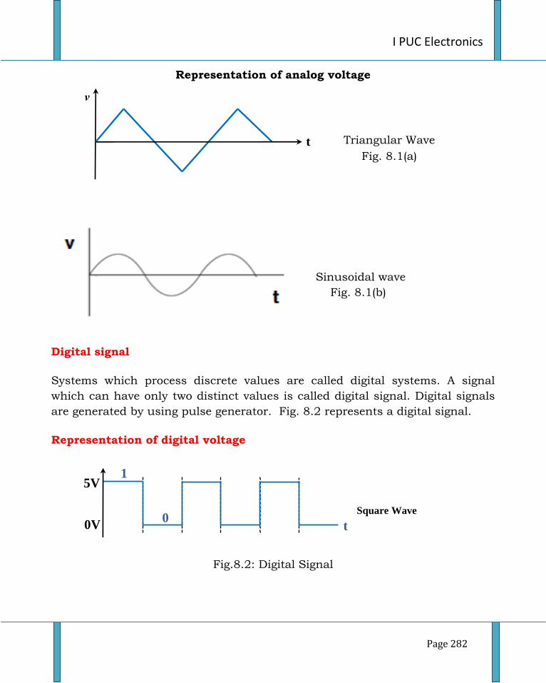
I PUC Electronics
Page 282
Representation of analog voltage
Sinusoidal wave
Fig. 8.1(b)
Digital signal
Systems which process discrete values are called digital systems. A signal
which can have only two distinct values is called digital signal. Digital signals
are generated by using pulse generator. Fig. 8.2 represents a digital signal.
Representation of digital voltage
Fig.8.2: Digital Signal
v
Triangular Wave
Fig. 8.1(a)
t
Square Wave
0V
5V 1
0 t
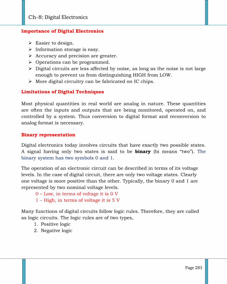
Ch-8: Digital Electronics
Page 283
Importance of Digital Electronics
Easier to design.
Information storage is easy.
Accuracy and precision are greater.
Operations can be programmed.
Digital circuits are less affected by noise, as long as the noise is not large
enough to prevent us from distinguishing HIGH from LOW.
More digital circuitry can be fabricated on IC chips.
Limitations of Digital Techniques
Most physical quantities in real world are analog in nature. These quantities
are often the inputs and outputs that are being monitored, operated on, and
controlled by a system. Thus conversion to digital format and reconversion to
analog format is necessary.
Binary representation
Digital electronics today involves circuits that have exactly two possible states.
A signal having only two states is said to be binary (bi means “two”). The
binary system has two symbols 0 and 1.
The operation of an electronic circuit can be described in terms of its voltage
levels. In the case of digital circuit, there are only two voltage states. Clearly
one voltage is more positive than the other. Typically, the binary 0 and 1 are
represented by two nominal voltage levels.
0 – Low, in terms of voltage it is 0 V
1 – High, in terms of voltage it is 5 V
Many functions of digital circuits follow logic rules. Therefore, they are called
as logic circuits. The logic rules are of two types,
1. Positive logic
2. Negative logic
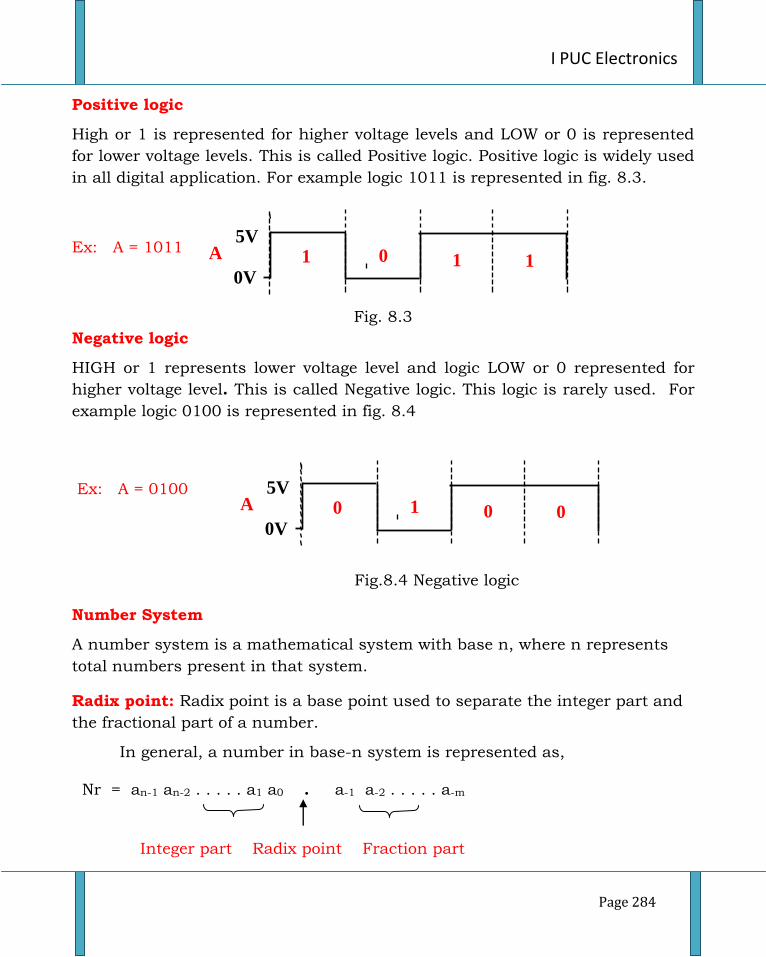
I PUC Electronics
Page 284
Positive logic
High or 1 is represented for higher voltage levels and LOW or 0 is represented
for lower voltage levels. This is called Positive logic. Positive logic is widely used
in all digital application. For example logic 1011 is represented in fig. 8.3.
Ex: A = 1011
Fig. 8.3
Negative logic
HIGH or 1 represents lower voltage level and logic LOW or 0 represented for
higher voltage level. This is called Negative logic. This logic is rarely used. For
example logic 0100 is represented in fig. 8.4
Ex: A = 0100
Fig.8.4 Negative logic
Number System
A number system is a mathematical system with base n, where n represents
total numbers present in that system.
Radix point: Radix point is a base point used to separate the integer part and
the fractional part of a number.
In general, a number in base-n system is represented as,
Nr = an-1 an-2 . . . . . a1 a0 . a-1 a-2 . . . . . a-m
Integer part Radix point Fraction part
0V 1
5V
1 0 1 A
0V 0
5V
0 1 0 A
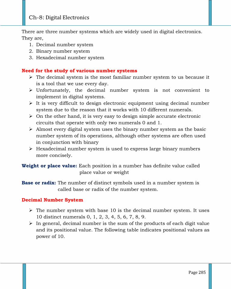
Ch-8: Digital Electronics
Page 285
There are three number systems which are widely used in digital electronics.
They are,
1. Decimal number system
2. Binary number system
3. Hexadecimal number system
Need for the study of various number systems
The decimal system is the most familiar number system to us because it
is a tool that we use every day.
Unfortunately, the decimal number system is not convenient to
implement in digital systems.
It is very difficult to design electronic equipment using decimal number
system due to the reason that it works with 10 different numerals.
On the other hand, it is very easy to design simple accurate electronic
circuits that operate with only two numerals 0 and 1.
Almost every digital system uses the binary number system as the basic
number system of its operations, although other systems are often used
in conjunction with binary
Hexadecimal number system is used to express large binary numbers
more concisely.
Weight or place value: Each position in a number has definite value called
place value or weight
Base or radix: The number of distinct symbols used in a number system is
called base or radix of the number system.
Decimal Number System
The number system with base 10 is the decimal number system. It uses
10 distinct numerals 0, 1, 2, 3, 4, 5, 6, 7, 8, 9.
In general, decimal number is the sum of the products of each digit value
and its positional value. The following table indicates positional values as
power of 10.
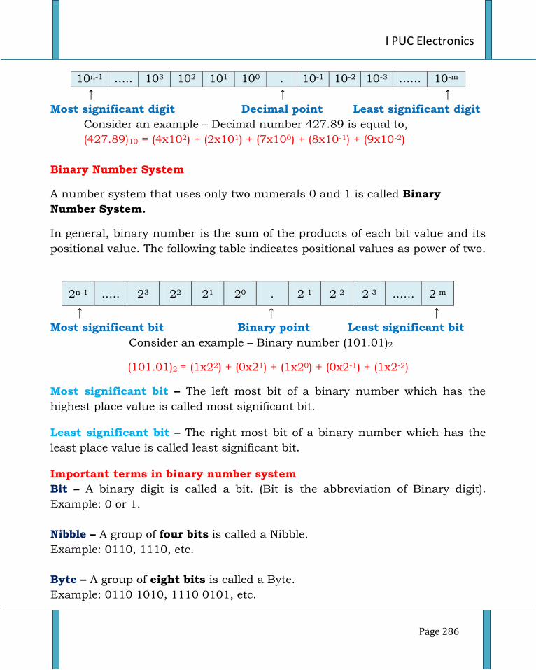
I PUC Electronics
Page 286
↑ ↑ ↑
Most significant digit Decimal point Least significant digit
Consider an example – Decimal number 427.89 is equal to,
(427.89)10 = (4x10²) + (2x101) + (7x100) + (8x10⁻¹) + (9x10⁻²)
Binary Number System
A number system that uses only two numerals 0 and 1 is called Binary
Number System.
In general, binary number is the sum of the products of each bit value and its
positional value. The following table indicates positional values as power of two.
2n-1 ….. 23 22 21 20 . 2-1 2-2 2-3 …… 2-m
↑ ↑ ↑
Most significant bit Binary point Least significant bit
Consider an example – Binary number (101.01)2
(101.01)2 = (1x22) + (0x21) + (1x20) + (0x2-1) + (1x2-2)
Most significant bit – The left most bit of a binary number which has the
highest place value is called most significant bit.
Least significant bit – The right most bit of a binary number which has the
least place value is called least significant bit.
Important terms in binary number system
Bit – A binary digit is called a bit. (Bit is the abbreviation of Binary digit).
Example: 0 or 1.
Nibble – A group of four bits is called a Nibble.
Example: 0110, 1110, etc.
Byte – A group of eight bits is called a Byte.
Example: 0110 1010, 1110 0101, etc.
10n-1 ….. 103 102 101 100 . 10-1 10-2 10-3 …… 10-m
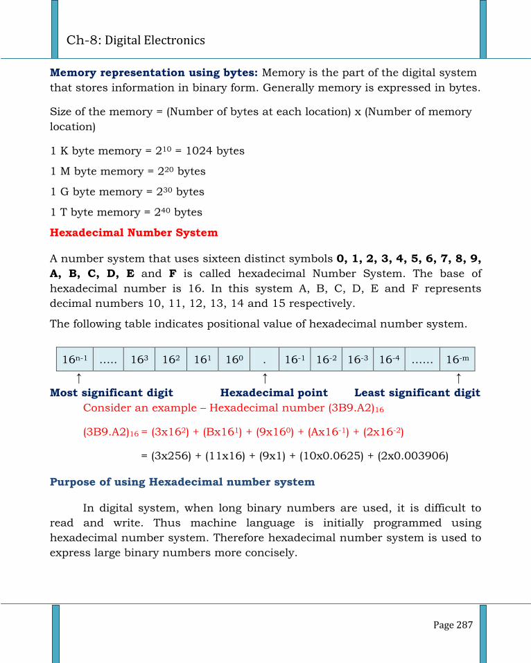
Ch-8: Digital Electronics
Page 287
Memory representation using bytes: Memory is the part of the digital system
that stores information in binary form. Generally memory is expressed in bytes.
Size of the memory = (Number of bytes at each location) x (Number of memory
location)
1 K byte memory = 210 = 1024 bytes
1 M byte memory = 220 bytes
1 G byte memory = 230 bytes
1 T byte memory = 240 bytes
Hexadecimal Number System
A number system that uses sixteen distinct symbols 0, 1, 2, 3, 4, 5, 6, 7, 8, 9,
A, B, C, D, E and F is called hexadecimal Number System. The base of
hexadecimal number is 16. In this system A, B, C, D, E and F represents
decimal numbers 10, 11, 12, 13, 14 and 15 respectively.
The following table indicates positional value of hexadecimal number system.
16n-1 ….. 163 162 161 160 . 16-1 16-2 16-3 16-4 …… 16-m
↑ ↑ ↑
Most significant digit Hexadecimal point Least significant digit
Consider an example – Hexadecimal number (3B9.A2)16
(3B9.A2)16 = (3x162) + (Bx161) + (9x160) + (Ax16-1) + (2x16-2)
= (3x256) + (11x16) + (9x1) + (10x0.0625) + (2x0.003906)
Purpose of using Hexadecimal number system
In digital system, when long binary numbers are used, it is difficult to
read and write. Thus machine language is initially programmed using
hexadecimal number system. Therefore hexadecimal number system is used to
express large binary numbers more concisely.
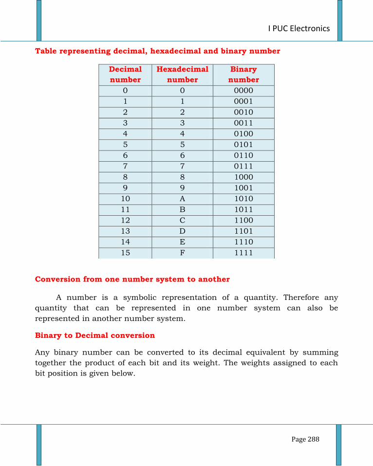
I PUC Electronics
Page 288
Table representing decimal, hexadecimal and binary number
Conversion from one number system to another
A number is a symbolic representation of a quantity. Therefore any
quantity that can be represented in one number system can also be
represented in another number system.
Binary to Decimal conversion
Any binary number can be converted to its decimal equivalent by summing
together the product of each bit and its weight. The weights assigned to each
bit position is given below.
Decimal
number
Hexadecimal
number
Binary
number
0 0 0000
1 1 0001
2 2 0010
3 3 0011
4 4 0100
5 5 0101
6 6 0110
7 7 0111
8 8 1000
9 9 1001
10 A 1010
11 B 1011
12 C 1100
13 D 1101
14 E 1110
15 F 1111
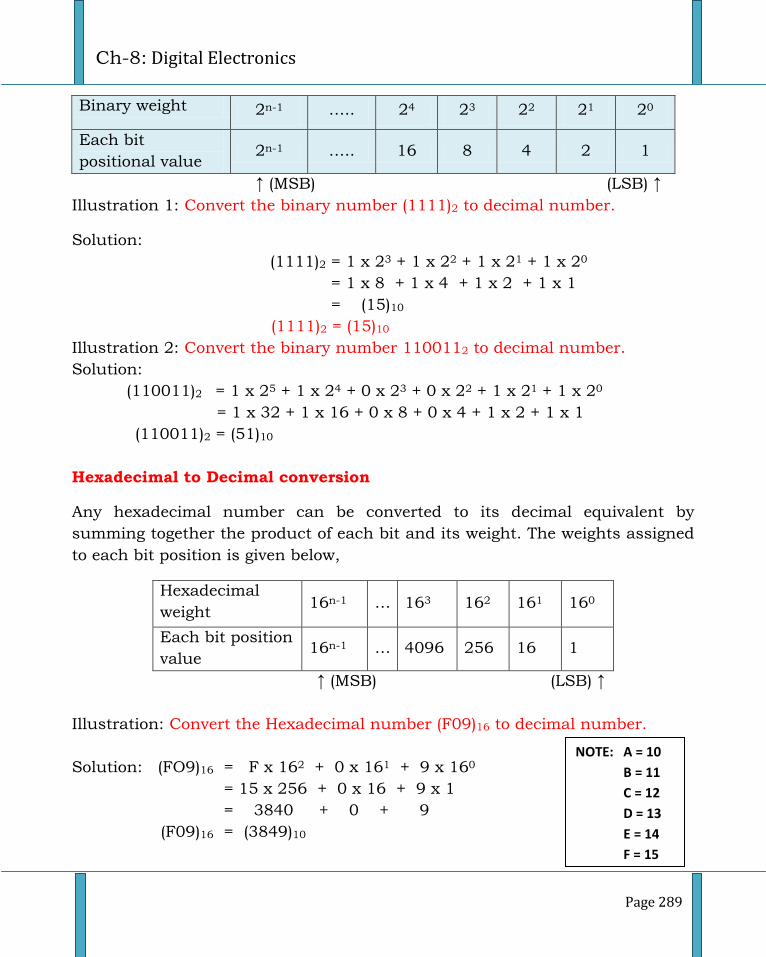
Ch-8: Digital Electronics
Page 289
Binary weight 2n-1 ….. 24 23 22 21 20
Each bit
positional value 2n-1 ….. 16 8 4 2 1
↑ (MSB) (LSB) ↑
Illustration 1: Convert the binary number (1111)2 to decimal number.
Solution:
(1111)2 = 1 x 23 + 1 x 22 + 1 x 21 + 1 x 20
= 1 x 8 + 1 x 4 + 1 x 2 + 1 x 1
= (15)10
(1111)2 = (15)10
Illustration 2: Convert the binary number 1100112 to decimal number.
Solution:
(110011)2 = 1 x 25 + 1 x 24 + 0 x 23 + 0 x 22 + 1 x 21 + 1 x 20
= 1 x 32 + 1 x 16 + 0 x 8 + 0 x 4 + 1 x 2 + 1 x 1
(110011)2 = (51)10
Hexadecimal to Decimal conversion
Any hexadecimal number can be converted to its decimal equivalent by
summing together the product of each bit and its weight. The weights assigned
to each bit position is given below,
Hexadecimal
weight 16n-1 … 163 162 161 160
Each bit position
value 16n-1 … 4096 256 16 1
↑ (MSB) (LSB) ↑
Illustration: Convert the Hexadecimal number (F09)16 to decimal number.
Solution: (FO9)16 = F x 162 + 0 x 161 + 9 x 160
= 15 x 256 + 0 x 16 + 9 x 1
= 3840 + 0 + 9
(F09)16 = (3849)10
NOTE: A = 10
B = 11
C = 12
D = 13
E = 14
F = 15
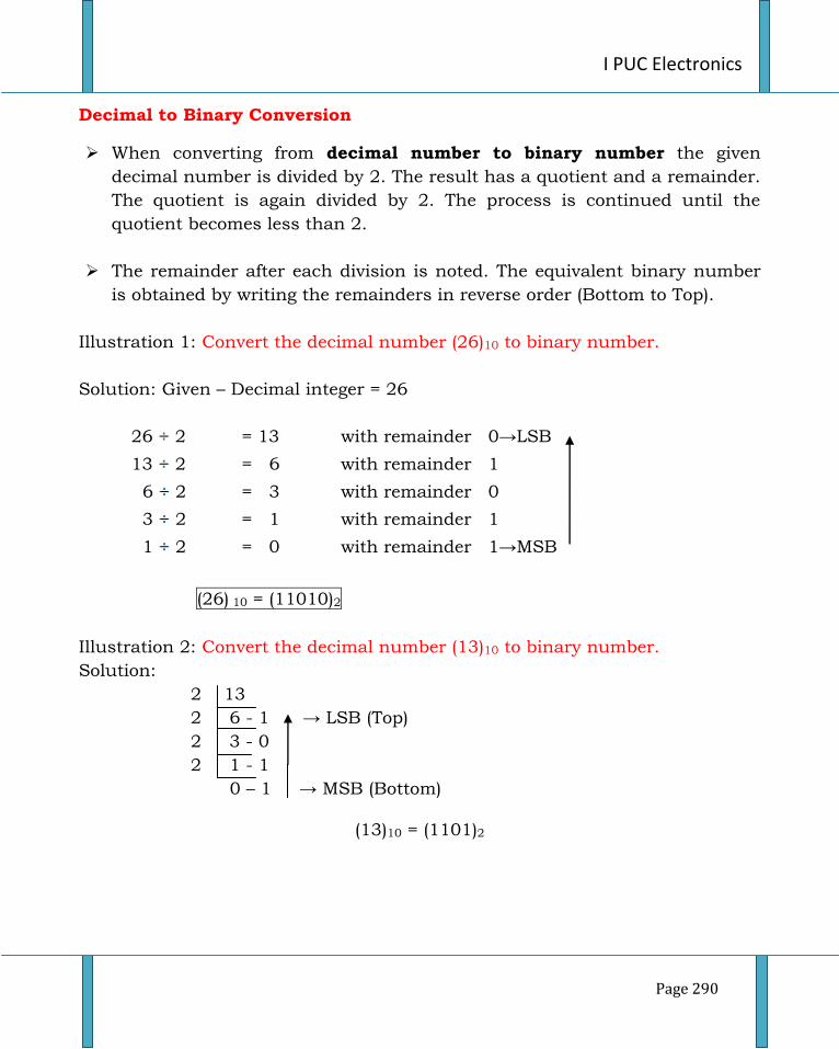
I PUC Electronics
Page 290
Decimal to Binary Conversion
When converting from decimal number to binary number the given
decimal number is divided by 2. The result has a quotient and a remainder.
The quotient is again divided by 2. The process is continued until the
quotient becomes less than 2.
The remainder after each division is noted. The equivalent binary number
is obtained by writing the remainders in reverse order (Bottom to Top).
Illustration 1: Convert the decimal number (26)10 to binary number.
Solution: Given – Decimal integer = 26
26 2 = 13 with remainder 0→LSB
13 2 = 6 with remainder 1
6 2 = 3 with remainder 0
3 2 = 1 with remainder 1
1 2 = 0 with remainder 1→MSB
(26) 10 = (11010)2
Illustration 2: Convert the decimal number (13)10 to binary number.
Solution:
2 13
2 6 - 1 → LSB (Top)
2 3 - 0
2 1 - 1
0 – 1 → MSB (Bottom)
(13)10 = (1101)2
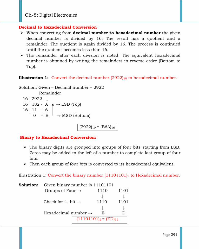
Ch-8: Digital Electronics
Page 291
Decimal to Hexadecimal Conversion
When converting from decimal number to hexadecimal number the given
decimal number is divided by 16. The result has a quotient and a
remainder. The quotient is again divided by 16. The process is continued
until the quotient becomes less than 16.
The remainder after each division is noted. The equivalent hexadecimal
number is obtained by writing the remainders in reverse order (Bottom to
Top).
Illustration 1: Convert the decimal number (2922)10 to hexadecimal number.
Solution: Given – Decimal number = 2922
Remainder
16 2922 ↓
16 182 - A → LSD (Top)
16 11 - 6
0 - B → MSD (Bottom)
(2922)10 = (B6A)16
Binary to Hexadecimal Conversion:
The binary digits are grouped into groups of four bits starting from LSB.
Zeros may be added to the left of a number to complete last group of four
bits.
Then each group of four bits is converted to its hexadecimal equivalent.
Illustration 1: Convert the binary number (11101101)2 to Hexadecimal number.
Solution: Given binary number is 11101101
Groups of Four → 1110 1101
↓ ↓
Check for 4- bit → 1110 1101
↓ ↓
Hexadecimal number → E D
(11101101)2 = (ED)16
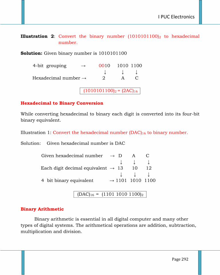
I PUC Electronics
Page 292
Illustration 2: Convert the binary number (1010101100)2 to hexadecimal
number.
Solution: Given binary number is 1010101100
4-bit grouping → 0010 1010 1100
↓ ↓ ↓
Hexadecimal number → 2 A C
(1010101100)2 = (2AC)16
Hexadecimal to Binary Conversion
While converting hexadecimal to binary each digit is converted into its four-bit
binary equivalent.
Illustration 1: Convert the hexadecimal number (DAC)16 to binary number.
Solution: Given hexadecimal number is DAC
Given hexadecimal number → D A C
↓ ↓ ↓
Each digit decimal equivalent → 13 10 12
↓ ↓ ↓
4 bit binary equivalent → 1101 1010 1100
Binary Arithmetic
Binary arithmetic is essential in all digital computer and many other
types of digital systems. The arithmetical operations are addition, subtraction,
multiplication and division.
(DAC)16 = (1101 1010 1100)2
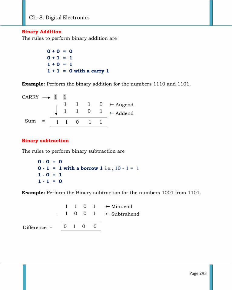
Ch-8: Digital Electronics
Page 293
Binary Addition
The rules to perform binary addition are
0 + 0 = 0
0 + 1 = 1
1 + 0 = 1
1 + 1 = 0 with a carry 1
Example: Perform the binary addition for the numbers 1110 and 1101.
CARRY 1 1
Augend
Addend
Sum =
Binary subtraction
The rules to perform binary subtraction are
0 - 0 = 0
0 - 1 = 1 with a borrow 1 i.e., 10 - 1 = 1
1 - 0 = 1
1 - 1 = 0
Example: Perform the Binary subtraction for the numbers 1001 from 1101.
Minuend
Subtrahend
Difference =
1 1 1 0
1 1 0 1
1 1 0 1 1
1 1 0 1
- 1 0 0 1
0 1 0 0
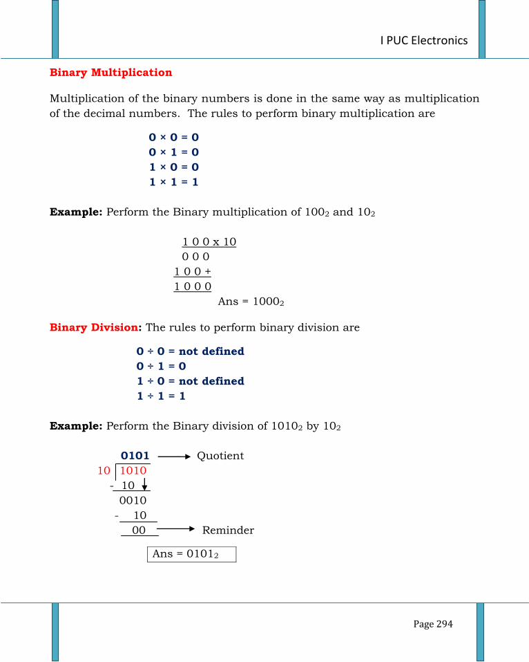
I PUC Electronics
Page 294
Binary Multiplication
Multiplication of the binary numbers is done in the same way as multiplication
of the decimal numbers. The rules to perform binary multiplication are
0 × 0 = 0
0 × 1 = 0
1 × 0 = 0
1 × 1 = 1
Example: Perform the Binary multiplication of 1002 and 102
1 0 0 x 10
0 0 0
1 0 0 +
1 0 0 0
Ans = 10002
Binary Division: The rules to perform binary division are
0 ÷ 0 = not defined
0 ÷ 1 = 0
1 ÷ 0 = not defined
1 ÷ 1 = 1
Example: Perform the Binary division of 10102 by 102
0101 Quotient
10 1010
- 10
0010
- 10
00 Reminder
Ans = 01012
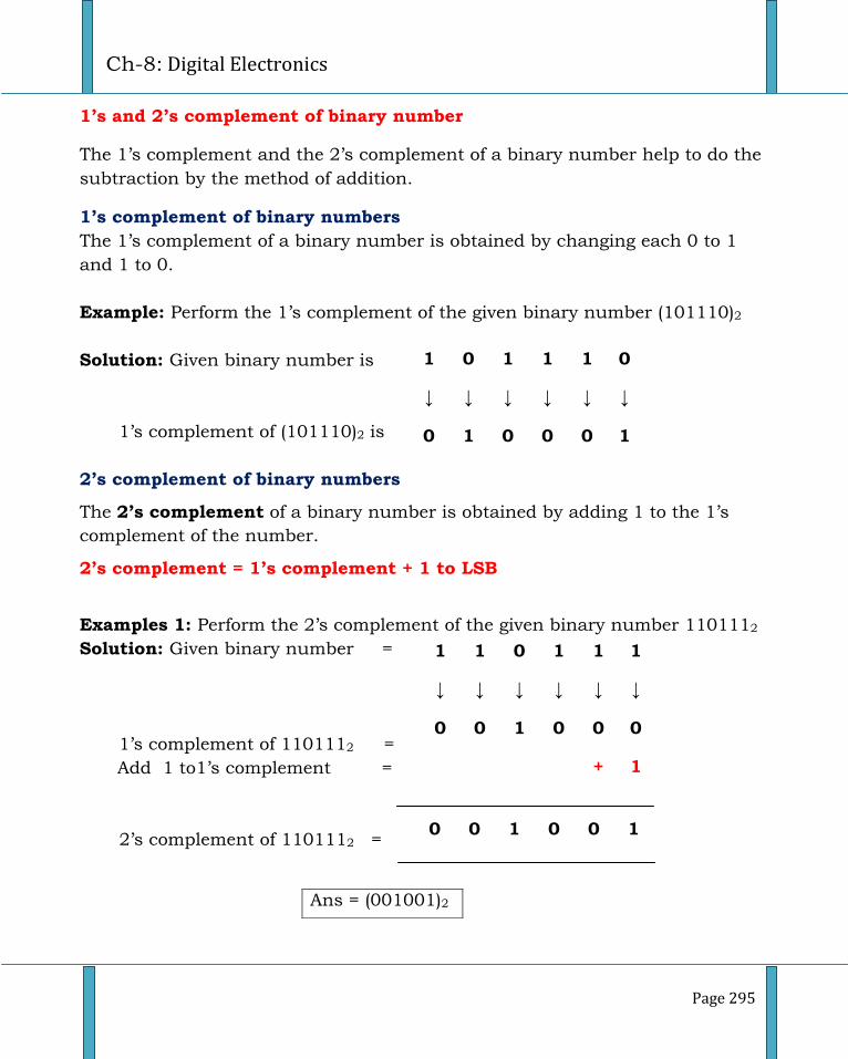
Ch-8: Digital Electronics
Page 295
1’s and 2’s complement of binary number
The 1’s complement and the 2’s complement of a binary number help to do the
subtraction by the method of addition.
1’s complement of binary numbers
The 1’s complement of a binary number is obtained by changing each 0 to 1
and 1 to 0.
Example: Perform the 1’s complement of the given binary number (101110)2
Solution: Given binary number is
1’s complement of (101110)2 is
2’s complement of binary numbers
The 2’s complement of a binary number is obtained by adding 1 to the 1’s
complement of the number.
2’s complement = 1’s complement + 1 to LSB
Examples 1: Perform the 2’s complement of the given binary number 1101112
Solution: Given binary number =
1’s complement of 1101112 =
Add 1 to1’s complement =
2’s complement of 1101112 =
1 0 1 1 1 0
↓ ↓ ↓ ↓ ↓ ↓
0 1 0 0 0 1
1 1 0 1 1 1
↓ ↓ ↓ ↓ ↓ ↓
0 0 1 0 0 0
+ 1
0 0 1 0 0 1
Ans = (001001)2
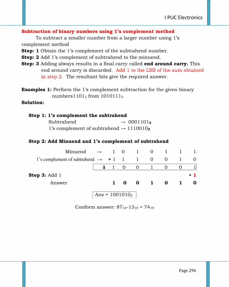
I PUC Electronics
Page 296
Subtraction of binary numbers using 1’s complement method
To subtract a smaller number from a larger number using 1’s
complement method
Step: 1 Obtain the 1’s complement of the subtrahend number.
Step: 2 Add 1’s complement of subtrahend to the minuend.
Step: 3 Adding always results in a final carry called end around carry. This
end around carry is discarded. Add 1 to the LSB of the sum obtained
in step 2. The resultant bits give the required answer.
Examples 1: Perform the 1’s complement subtraction for the given binary
numbers11012 from 10101112
Solution:
Step 1: 1’s complement the subtrahend
Subtrahend → 00011012
1’s complement of subtrahend → 11100102
Step 2: Add Minuend and 1’s complement of subtrahend
Minuend → 1 0 1 0 1 1 1
1’s complement of subtrahend → + 1 1 1 0 0 1 0
1 1 0 0 1 0 0 1
Step 3: Add 1 + 1
Answer 1 0 0 1 0 1 0
Conform answer: 8710-1310 = 7410
Ans = 10010102
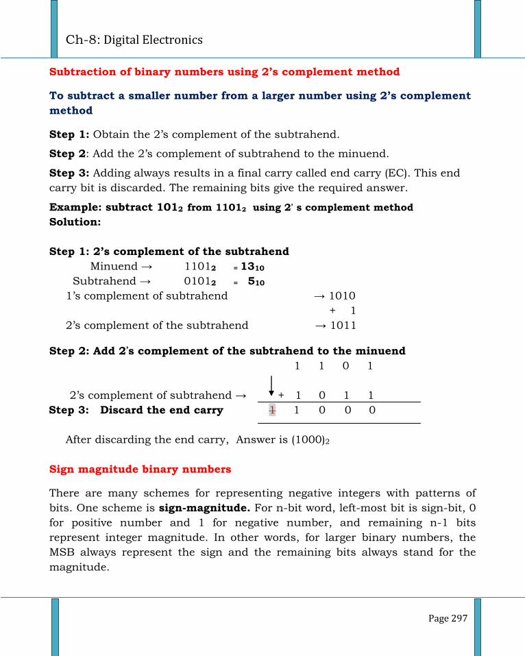
Ch-8: Digital Electronics
Page 297
Subtraction of binary numbers using 2’s complement method
To subtract a smaller number from a larger number using 2’s complement
method
Step 1: Obtain the 2’s complement of the subtrahend.
Step 2: Add the 2’s complement of subtrahend to the minuend.
Step 3: Adding always results in a final carry called end carry (EC). This end
carry bit is discarded. The remaining bits give the required answer.
Example: subtract 1012 from 11012 using 2’ s complement method
Solution:
Step 1: 2’s complement of the subtrahend
Minuend → 11012 = 1310
Subtrahend → 01012 = 510
1’s complement of subtrahend → 1010
+ 1
2’s complement of the subtrahend → 1011
Step 2: Add 2’s complement of the subtrahend to the minuend
1 1 0 1
2’s complement of subtrahend → + 1 0 1 1
Step 3: Discard the end carry 1 1 0 0 0
After discarding the end carry, Answer is (1000)2
Sign magnitude binary numbers
There are many schemes for representing negative integers with patterns of
bits. One scheme is sign-magnitude. For n-bit word, left-most bit is sign-bit, 0
for positive number and 1 for negative number, and remaining n-1 bits
represent integer magnitude. In other words, for larger binary numbers, the
MSB always represent the sign and the remaining bits always stand for the
magnitude.
I PUC Electronics
Page 298
Representing a sign magnitude numbers
Given number is 2510 = 110012
Then 0 11001 = +25
1 11001 = -25
In the above example 0 in the MSB position represents +ve and 1 in the MSB
position represents –ve number.
Boolean Algebra
Boolean algebra is the study of ‘mathematical theory of logic’. It was
initially formulated by George Boole, a mathematician. In Boolean algebra,
each variable can only assume one of the two values 1 and 0. It is used in the
design, maintenance and analysis of digital circuits.
Boolean operations
The basic logic operations are
1) OR operation (Boolean addition)
2) AND operation (Boolean multiplication)
3) NOT operation (Boolean negation)
OR operation
1) A + 0 = A
2) A + 1 = 1
3) A + A = A
4) A + = 1
Ch-8: Digital Electronics
Page 299
AND operation
1) A·0 = 0
2) A·1 = A
3) A·A = A
4) A· = 0
NOT operation
= A
Basic Laws and Theorems of Boolean Algebra
Commutative laws
1) A+B = B+A
2) AB = BA
Associative laws
1) A(BC) = (AB)C
2) A+(B+C) = (A+B)+C
Distributive laws
1) A(B+C) = AB+AC
2) A+BC = (A+B)(A+C)
Other Boolean laws
1) A+AB = A
2) A+ B = A+B
3) AB + A = A
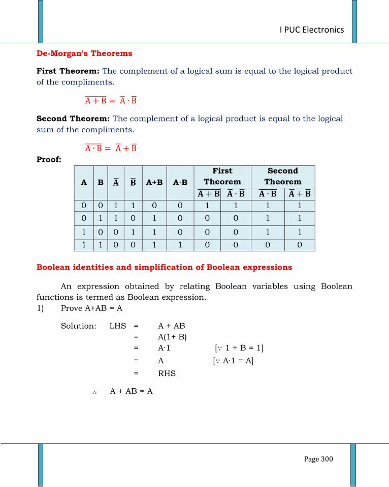
I PUC Electronics
Page 300
De-Morgan's Theorems
First Theorem: The complement of a logical sum is equal to the logical product
of the compliments.
Second Theorem: The complement of a logical product is equal to the logical
sum of the compliments.
Proof:
A B A+B A·B
First
Theorem
Second
Theorem
0 0 1 1 0 0 1 1 1 1
0 1 1 0 1 0 0 0 1 1
1 0 0 1 1 0 0 0 1 1
1 1 0 0 1 1 0 0 0 0
Boolean identities and simplification of Boolean expressions
An expression obtained by relating Boolean variables using Boolean
functions is termed as Boolean expression.
1) Prove A+AB = A
Solution: LHS = A + AB
= A(1+ B)
= A·1 [ 1 + B = 1]
= A [ A·1 = A]
= RHS
A + AB = A
Ch-8: Digital Electronics
Page 301
2) Prove A + BC = (A + B)(A + C)
Solution : Consider RHS
(A+B)(A+C) = A·A + A·C + B·A + B·C
= A + AC + AB + BC
= A(1+ C) + AB + BC
= A·1 + AB + BC
= A + AB + BC
= A(1+ B) +BC
= A·1 + BC
= A + BC
= LHS
A+BC = (A+B)(A+C)
3) Prove (A+ B) = A+B
Solution : LHS = A + B
We know that (A+BC) = (A+B)(A+C)
(A+ B) = (A+ )(A+B)
= 1· (A+B)
= A+B
= RHS
(A+ B) = A+B
4) Simplify the equation Y = A C + BC + ABC
Solution : Y = A C + BC + ABC
= A C + BC ( +A)
= A C + (BC·1)
= A C + BC
= C[B+ A]
= C(B+A)
Y = BC + AC
I PUC Electronics
Page 302
5) Simplify the equation Y = AB + A( )
Solution: Y = AB + A( )
= AB + A ( · )
= AB + A
= A ( B+ )
= A ( B+ )
= AB + A
6) Simplify the equation Y = ( )
Solution: Y =
=
= ( ·A) + ( ·B)
= ( + )A + ( + )B
= ( A + A) + B + B
= 0 + A + B + 0
Y = A + B
7) Simplify the equation Y = + C
Solution : Y = + C
= + C
= ( + )( + )+ C
= + + C
= + ( + C )
= + ( + )
= + +
= (1+ ) +
= ·1 +
= +
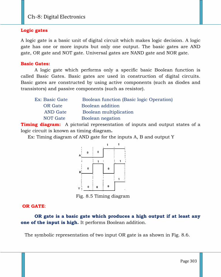
Ch-8: Digital Electronics
Page 303
Logic gates
A logic gate is a basic unit of digital circuit which makes logic decision. A logic
gate has one or more inputs but only one output. The basic gates are AND
gate, OR gate and NOT gate. Universal gates are NAND gate and NOR gate.
Basic Gates:
A logic gate which performs only a specific basic Boolean function is
called Basic Gates. Basic gates are used in construction of digital circuits.
Basic gates are constructed by using active components (such as diodes and
transistors) and passive components (such as resistor).
Ex: Basic Gate Boolean function (Basic logic Operation)
OR Gate Boolean addition
AND Gate Boolean multiplication
NOT Gate Boolean negation
Timing diagram: A pictorial representation of inputs and output states of a
logic circuit is known as timing diagram.
Ex: Timing diagram of AND gate for the inputs A, B and output Y
Fig. 8.5 Timing diagram
OR GATE:
OR gate is a basic gate which produces a high output if at least any
one of the input is high. It performs Boolean addition.
The symbolic representation of two input OR gate is as shown in Fig. 8.6.
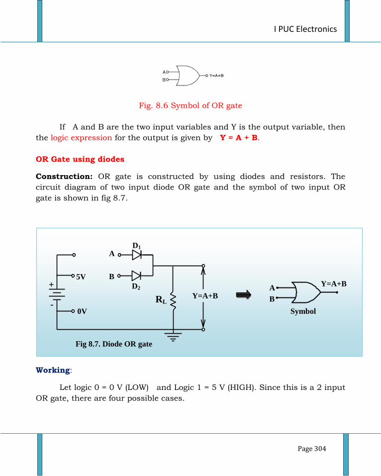
I PUC Electronics
Page 304
Fig. 8.6 Symbol of OR gate
If A and B are the two input variables and Y is the output variable, then
the logic expression for the output is given by Y = A + B.
OR Gate using diodes
Construction: OR gate is constructed by using diodes and resistors. The
circuit diagram of two input diode OR gate and the symbol of two input OR
gate is shown in fig 8.7.
Working:
Let logic 0 = 0 V (LOW) and Logic 1 = 5 V (HIGH). Since this is a 2 input
OR gate, there are four possible cases.
RL Y=A+B
B
D1
D2 +
-
A
0V
5V
A
B
Symbol
Y=A+B
Fig 8.7. Diode OR gate
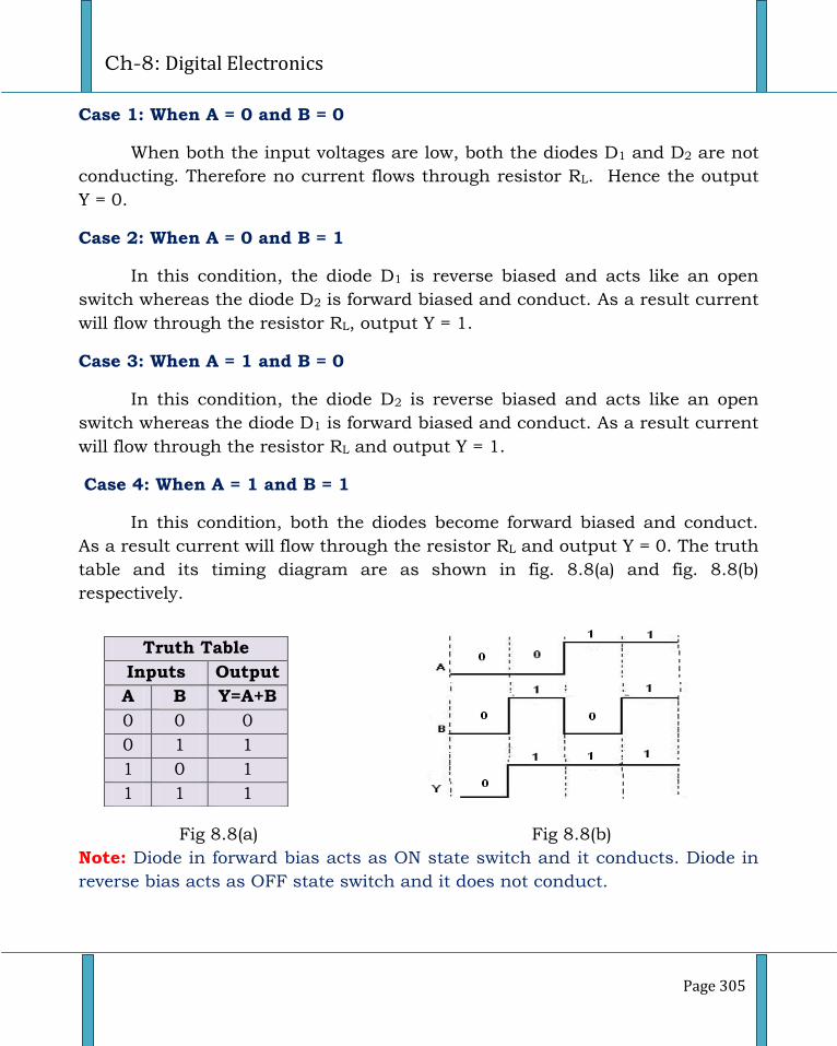
Ch-8: Digital Electronics
Page 305
Case 1: When A = 0 and B = 0
When both the input voltages are low, both the diodes D1 and D2 are not
conducting. Therefore no current flows through resistor RL. Hence the output
Y = 0.
Case 2: When A = 0 and B = 1
In this condition, the diode D1 is reverse biased and acts like an open
switch whereas the diode D2 is forward biased and conduct. As a result current
will flow through the resistor RL, output Y = 1.
Case 3: When A = 1 and B = 0
In this condition, the diode D2 is reverse biased and acts like an open
switch whereas the diode D1 is forward biased and conduct. As a result current
will flow through the resistor RL and output Y = 1.
Case 4: When A = 1 and B = 1
In this condition, both the diodes become forward biased and conduct.
As a result current will flow through the resistor RL and output Y = 0. The truth
table and its timing diagram are as shown in fig. 8.8(a) and fig. 8.8(b)
respectively.
Fig 8.8(a) Fig 8.8(b)
Note: Diode in forward bias acts as ON state switch and it conducts. Diode in
reverse bias acts as OFF state switch and it does not conduct.
Truth Table
Inputs Output
A B Y=A+B
0 0 0
0 1 1
1 0 1
1 1 1
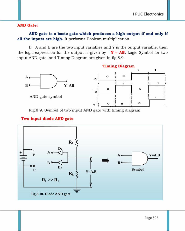
I PUC Electronics
Page 306
AND Gate:
AND gate is a basic gate which produces a high output if and only if
all the inputs are high. It performs Boolean multiplication.
If A and B are the two input variables and Y is the output variable, then
the logic expression for the output is given by Y = AB. Logic Symbol for two
input AND gate, and Timing Diagram are given in fig 8.9.
Timing Diagram
AND gate symbol
Fig.8.9. Symbol of two input AND gate with timing diagram
Two input diode AND gate
RL Y=A.B
B 0
V
D1
D2
+ A 5
V
R1
-
A
B
Y=A.B
Symbol
Fig 8.10. Diode AND gate
RL >> R1
B Y=AB
A
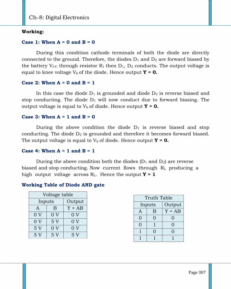
Ch-8: Digital Electronics
Page 307
Working:
Case 1: When A = 0 and B = 0
During this condition cathode terminals of both the diode are directly
connected to the ground. Therefore, the diodes D1 and D2 are forward biased by
the battery VCC through resistor R1 then D1, D2 conducts. The output voltage is
equal to knee voltage Vk of the diode. Hence output Y = 0.
Case 2: When A = 0 and B = 1
In this case the diode D1 is grounded and diode D2 is reverse biased and
stop conducting. The diode D1 will now conduct due to forward biasing. The
output voltage is equal to Vk of diode. Hence output Y = 0.
Case 3: When A = 1 and B = 0
During the above condition the diode D1 is reverse biased and stop
conducting. The diode D2 is grounded and therefore it becomes forward biased.
The output voltage is equal to Vk of diode. Hence output Y = 0.
Case 4: When A = 1 and B = 1
During the above condition both the diodes (D1 and D2) are reverse
biased and stop conducting. Now current flows through RL producing a
high output voltage across RL. Hence the output Y = 1
Working Table of Diode AND gate
Truth Table
Inputs Output
A B Y = AB
0 0 0
0 1 0
1 0 0
1 1 1
Voltage table
Inputs Output
A B Y = AB
0 V 0 V 0 V
0 V 5 V 0 V
5 V 0 V 0 V
5 V 5 V 5 V
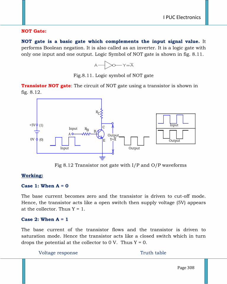
I PUC Electronics
Page 308
NOT Gate:
NOT gate is a basic gate which complements the input signal value. It
performs Boolean negation. It is also called as an inverter. It is a logic gate with
only one input and one output. Logic Symbol of NOT gate is shown in fig. 8.11.
Fig.8.11. Logic symbol of NOT gate
Transistor NOT gate: The circuit of NOT gate using a transistor is shown in
fig. 8.12.
(0)0V
(1)+5V
A
Input
Y=AOutput
RB
RC
CB
E
Input Output
Output
Input
Fig 8.12 Transistor not gate with I/P and O/P waveforms
Working:
Case 1: When A = 0
The base current becomes zero and the transistor is driven to cut-off mode.
Hence, the transistor acts like a open switch then supply voltage (5V) appears
at the collector. Thus Y = 1.
Case 2: When A = 1
The base current of the transistor flows and the transistor is driven to
saturation mode. Hence the transistor acts like a closed switch which in turn
drops the potential at the collector to 0 V. Thus Y = 0.
Voltage response Truth table
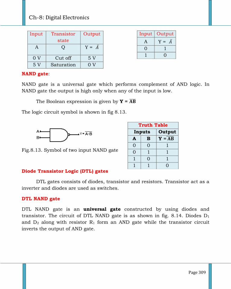
Ch-8: Digital Electronics
Page 309
NAND gate:
NAND gate is a universal gate which performs complement of AND logic. In
NAND gate the output is high only when any of the input is low.
The Boolean expression is given by Y =
The logic circuit symbol is shown in fig 8.13.
Fig.8.13. Symbol of two input NAND gate
Diode Transistor Logic (DTL) gates
DTL gates consists of diodes, transistor and resistors. Transistor act as a
inverter and diodes are used as switches.
DTL NAND gate
DTL NAND gate is an universal gate constructed by using diodes and
transistor. The circuit of DTL NAND gate is as shown in fig. 8.14. Diodes D1
and D2 along with resistor R1 form an AND gate while the transistor circuit
inverts the output of AND gate.
Input Output
A Y =
0 1
1 0
Input Transistor
state
Output
A Q Y =
0 V Cut off 5 V
5 V Saturation 0 V
Truth Table
Inputs Output
A B Y =
0 0 1
0 1 1
1 0 1
1 1 0
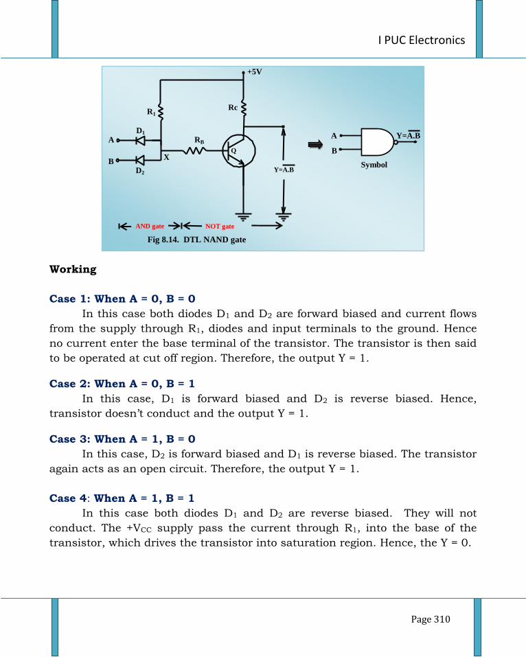
I PUC Electronics
Page 310
Working
Case 1: When A = 0, B = 0
In this case both diodes D1 and D2 are forward biased and current flows
from the supply through R1, diodes and input terminals to the ground. Hence
no current enter the base terminal of the transistor. The transistor is then said
to be operated at cut off region. Therefore, the output Y = 1.
Case 2: When A = 0, B = 1
In this case, D1 is forward biased and D2 is reverse biased. Hence,
transistor doesn’t conduct and the output Y = 1.
Case 3: When A = 1, B = 0
In this case, D2 is forward biased and D1 is reverse biased. The transistor
again acts as an open circuit. Therefore, the output Y = 1.
Case 4: When A = 1, B = 1
In this case both diodes D1 and D2 are reverse biased. They will not
conduct. The +VCC supply pass the current through R1, into the base of the
transistor, which drives the transistor into saturation region. Hence, the Y = 0.
R1
RB
Q
Rc
Y=A.B
+5V
X B
D1
D2
A
NOT gate AND gate
A
B
Y=A.B
Symbol
Fig 8.14. DTL NAND gate
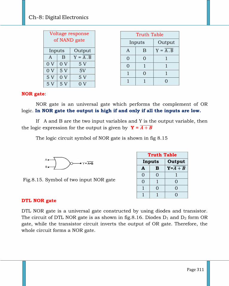
Ch-8: Digital Electronics
Page 311
NOR gate:
NOR gate is an universal gate which performs the complement of OR
logic. In NOR gate the output is high if and only if all the inputs are low.
If A and B are the two input variables and Y is the output variable, then
the logic expression for the output is given by Y =
The logic circuit symbol of NOR gate is shown in fig 8.15
Fig.8.15. Symbol of two input NOR gate
DTL NOR gate
DTL NOR gate is a universal gate constructed by using diodes and transistor.
The circuit of DTL NOR gate is as shown in fig.8.16. Diodes D1 and D2 form OR
gate, while the transistor circuit inverts the output of OR gate. Therefore, the
whole circuit forms a NOR gate.
Voltage response
of NAND gate
Inputs Output
A B Y =
0 V 0 V 5 V
0 V 5 V 5V
5 V 0 V 5 V
5 V 5 V 0 V
Truth Table
Inputs Output
A B Y =
0 0 1
0 1 1
1 0 1
1 1 0
Truth Table
Inputs Output
A B Y=
0 0 1
0 1 0
1 0 0
1 1 0
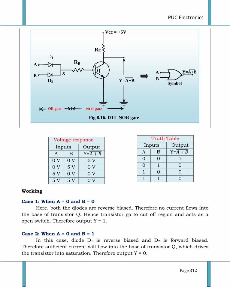
I PUC Electronics
Page 312
Working
Case 1: When A = 0 and B = 0
Here, both the diodes are reverse biased. Therefore no current flows into
the base of transistor Q. Hence transistor go to cut off region and acts as a
open switch. Therefore output Y = 1.
Case 2: When A = 0 and B = 1
In this case, diode D1 is reverse biased and D2 is forward biased.
Therefore sufficient current will flow into the base of transistor Q, which drives
the transistor into saturation. Therefore output Y = 0.
Truth Table
Inputs Output
A B Y=
0 0 1
0 1 0
1 0 0
1 1 0
Voltage response
Inputs Output
A B Y=
0 V 0 V 5 V
0 V 5 V 0 V
5 V 0 V 0 V
5 V 5 V 0 V
RB
Q
Rc
Y=A+B
Vcc = +5V
X B
D1
D2
A
NOT gate OR gate
A
B Symbol
Y=A+B
Fig 8.16. DTL NOR gate
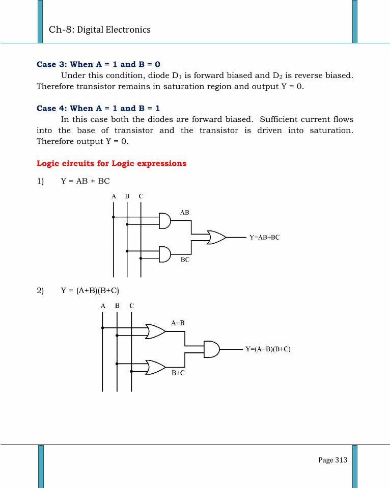
Ch-8: Digital Electronics
Page 313
Case 3: When A = 1 and B = 0
Under this condition, diode D1 is forward biased and D2 is reverse biased.
Therefore transistor remains in saturation region and output Y = 0.
Case 4: When A = 1 and B = 1
In this case both the diodes are forward biased. Sufficient current flows
into the base of transistor and the transistor is driven into saturation.
Therefore output Y = 0.
Logic circuits for Logic expressions
1) Y = AB + BC
2) Y = (A+B)(B+C)
I PUC Electronics
Page 314
3) Y = ( ) + BC
4) Y =
Pulse (clock) generator using 555.
Astable Multivibrator: The 555 timer is a Transistor - Transistor logic (TTL)
integrated circuit. It is used as an oscillator to provide a clock waveform to
digital circuits and many more timing applications. It has two distinct output
levels. Neither of the output levels is stable. Therefore this circuit is said to be
Astable Multivibrator. The timing capacitor is charged toward +VCC through
resistors RA and RB and then discharged towards ground by RB only. The
frequency of oscillation and duty cycle are accurately controlled by two external
resistors and a single timing capacitor.
Pin diagram of 555 timer is shown in fig 8.17(a). Circuit diagram of astable
multivibrator using LM555 is as shown in fig. 8.17(b). The output waveform is
showing fig. 8.17(c).
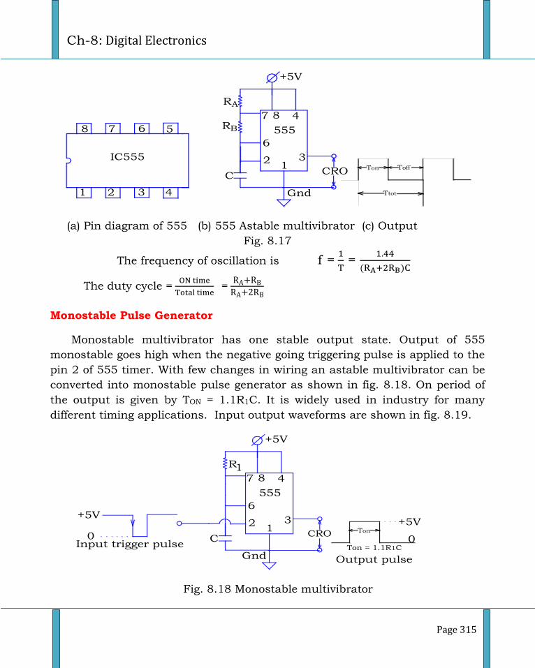
Ch-8: Digital Electronics
Page 315
CRO
+5V
8 4
Ton
6
Toff
C
21
3
7RB
RA
TtotGnd
555
1 2 3 4
8 7 6 5
IC555
(a) Pin diagram of 555 (b) 555 Astable multivibrator (c) Output
Fig. 8.17
The frequency of oscillation is f =
=
The duty cycle =
=
Monostable Pulse Generator
Monostable multivibrator has one stable output state. Output of 555
monostable goes high when the negative going triggering pulse is applied to the
pin 2 of 555 timer. With few changes in wiring an astable multivibrator can be
converted into monostable pulse generator as shown in fig. 8.18. On period of
the output is given by TON = 1.1R1C. It is widely used in industry for many
different timing applications. Input output waveforms are shown in fig. 8.19.
CRO
+5V
8 4
Ton
6
C
21
3
7
R1
Gnd
555
+5V
0Ton = 1.1R1CInput trigger pulse
Output pulse
+5V
0
Fig. 8.18 Monostable multivibrator
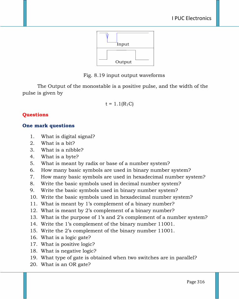
I PUC Electronics
Page 316
Output
Input
Fig. 8.19 input output waveforms
The Output of the monostable is a positive pulse, and the width of the
pulse is given by
t = 1.1(R1C)
Questions
One mark questions
1. What is digital signal?
2. What is a bit?
3. What is a nibble?
4. What is a byte?
5. What is meant by radix or base of a number system?
6. How many basic symbols are used in binary number system?
7. How many basic symbols are used in hexadecimal number system?
8. Write the basic symbols used in decimal number system?
9. Write the basic symbols used in binary number system?
10. Write the basic symbols used in hexadecimal number system?
11. What is meant by 1’s complement of a binary number?
12. What is meant by 2’s complement of a binary number?
13. What is the purpose of 1’s and 2’s complement of a number system?
14. Write the 1’s complement of the binary number 11001.
15. Write the 2’s complement of the binary number 11001.
16. What is a logic gate?
17. What is positive logic?
18. What is negative logic?
19. What type of gate is obtained when two switches are in parallel?
20. What is an OR gate?
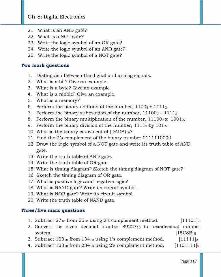
Ch-8: Digital Electronics
Page 317
21. What is an AND gate?
22. What is a NOT gate?
23. Write the logic symbol of an OR gate?
24. Write the logic symbol of an AND gate?
25. Write the logic symbol of a NOT gate?
Two mark questions
1. Distinguish between the digital and analog signals.
2. What is a bit? Give an example.
3. What is a byte? Give an example
4. What is a nibble? Give an example.
5. What is a memory?
6. Perform the binary addition of the number, 11002 + 11112.
7. Perform the binary subtraction of the number, 111002 – 11112.
8. Perform the binary multiplication of the number, 111002 x 10012.
9. Perform the binary division of the number, 11112 by 1012.
10. What is the binary equivalent of (DADA)16?
11. Find the 2’s complement of the binary number 0111110000
12. Draw the logic symbol of a NOT gate and write its truth table of AND
gate.
13. Write the truth table of AND gate.
14. Write the truth table of OR gate.
15. What is timing diagram? Sketch the timing diagram of NOT gate?
16. Sketch the timing diagram of OR gate.
17. What is positive logic and negative logic?
18. What is NAND gate? Write its circuit symbol.
19. What is NOR gate? Write its circuit symbol.
20. Write the truth table of NAND gate.
Three/five mark questions
1. Subtract 2710 from 5610 using 2’s complement method. [11101]2
2. Convert the given decimal number 8922710 to hexadecimal number
system. [15C8B]H
3. Subtract 10310 from 13410 using 1’s complement method. [11111]2
4. Subtract 12310 from 23410 using 2’s complement method. [1101111]2
I PUC Electronics
Page 318
5. Write the purpose of octal and hexadecimal number system.
6. Explain the transistor NOT gate.
7. Write the limitations of digital technology. Explain with a circuit diagram
the action of a 2 input diode OR gate.
8. Explain with a circuit diagram the action of a 2 input Diode AND gate.
9. Explain with a DTL circuit the action of 2 input NAND gate.
10. Explain the construction and working of DTL NOR gate
Problems
Convert the following decimal numbers to binary number:
1. 3710 [100101]2
2. 37510 [101110111]2
3. 43510 [110110011]2
4. 50010 [111110100]2
Convert the following binary numbers to decimal number:
1. 1101102 [54]10
2. 100011012 [141]10
3. 11111111112 [1023]10
4. 101100011112 [1423]10
Convert the following decimal numbers to hexadecimal number:
1. 333810 [D0A]16
2. 2375210 [5CC8]16
3. 677910 [1A7B]16
4. 78562210 [BFCD6]16
Convert the following hexadecimal numbers to decimal number:
1. 19416 [404]10
2. FE516 [4069]10
3. 4DD16 [1245]10
4. A75616 [42838]10
Ch-8: Digital Electronics
Page 319
Convert the following Binary numbers to Hexadecimal number:
1. 1001102 [26]16
2. 100011012 [8D]16
3. 11001111112 [33F]16
4. 10110001012 [2C5]16
Convert the following Hexadecimal numbers to Binary number:
1. CB0116 [1100 1011 0000 0001]2
2. 2FE5216 [0010 1111 1110 0101 0010]2
3. 4DD16 [0100 1101 1101]2
Problems on binary arithmetic
Perform the binary addition for the following
1. 101012 + 11112 [100100]2
2. 1112 + 011102 [10101]2
3. 10111112 +1110112 [10011010]2
4. 10110112 + 11010112 [11000110]2
Perform the Binary Subtraction for the following
1. 111012 - 100112 [1010]2
2. 1111112 - 011102 [110001]2
3. 110111112 -1110112 [10100100]2
4. 110110112 - 11010112 [1110000]2
Perform the Binary Multiplication for the following
1. 111012 x 102 [111010]2
2. 1111112 x 0112 [10111101]2
3. 11011112 x 1102 [1010011010]2
4. 1101112 x 1112 [110000001]2
Perform the Binary Division for the following
1. 11002 by 1002 [11]2
2. 1111112 by 10012 [111]2
3. 101002 by 1002 [101]2
4. 1000112 by 1112 [101]2
I PUC Electronics
Page 320
Perform the 1’s complement for the following Binary Numbers
1. 111012 [00010]2
2. 111110112 [00000100]2
3. 110110102 [00100101]2
4. 11011100002 [0010001111]2
Perform the 2’s complement for the following Binary Numbers
1. 11101112 [0001001]2
2. 111011112 [00010001]2
3. 110110102 [00100110]2
4. 11011100002 [0010010000]2
Perform the Binary Subtraction for the following using the 1’s complement
1. 111012 - 100112 [1010]2
2. 1111112 - 011102 [110001]2
3. 1101112 - 11102 [101001]2
4. 11011112 - 1101112 [111000]2
Perform the Binary Subtraction for the following using the 1’s complement
1. 5510 - 3210 [10111]2
2. 5510 - 1910 [100100]2
3. 8810 - 5610 [100000]2
4. 5810 - 1210 [101110]2
Perform the Binary Subtraction for the following using the 2’s complement
1. 5510 - 4210 [1101]2
2. 5910 - 1810 [101001]2
3. 9910 - 5610 [101011]2
4. 6710 - 1210 [110111]2
Perform the Binary Subtraction for the following using the 2’s complement
1. 110112 - 110012 [10]2
2. 1010012 - 101102 [10011]2
3. 1101112 - 1010112 [1100]2
4. 101010102 - 1101112 [1110011]2
Ch 9: Practical Electronic Components, their specifications and PCB
Page 321
Chapter-9
Practical Electronic Components, their specifications
and PCB
Introduction: Before constructing and testing a circuit a clear idea of the
availability of components for the particular applications is necessary. Also it
is important to know the specifications of each components used in the circuit
or project. All the components are available with their standard ratings. A
complete idea on specifications of each component is necessary during the
purchase of components from the shops. User should select the component
with correct specifications to construct the circuit. If the specifications of the
components are improperly selected they may be damaged due to over power,
over voltage, over current etc. The circuit is usually constructed on general
purpose boards which are readily available in shops. This chapter dealt with
commonly used components, their important specifications and development of
Printed Circuit Board.
Components part number
Specification of each component contains physical, mechanical and electrical
parameters. Each parameter of a device cannot be remembered at all the
times. All the specifications of a device are summarized and a part number is
given by the manufacturer. Data sheet of the part number provides detailed
specifications of the component. Part number is a unique code used to
identify a particular item (or component) for the convenience of consumers or
of manufacturer. Parts to be numbered usually include electrical items (wires,
cables, connectors, switches, soldering lugs, crocodile clips), electronic
components (diodes, transistors, integrated circuits).
Data sheet
A datasheet or specification sheet is a document summarizing the
performance and other technical characteristics of a component (e.g. an
electronic component) or a subsystem (e.g. a power supply). Typically, a
I PUC Electronics
Page 322
datasheet is created by the component or subsystem manufacturer. A data
sheet is usually used for technical communication to describe technical
characteristics of an item or product. It can be published by the manufacturer
to help people choose products or to help to use the products.
A typical datasheet for an electronic component contains the following
information:
Manufacturer's name
Product number and name
List of available package formats (with images) and ordering codes
Functional descriptions
Pin connection diagram
Absolute minimum, maximum ratings (supply voltage, power
consumption, temperatures range, etc.)
Recommended operating conditions
Graphs showing variations of parameters
Input/output wave shape diagram
Physical details showing dimensions.
Test circuits.
Package:
A package of an electronic component gives details on body size, mount area,
thickness, pins, pitch of the pins, power dissipation, tapping directions etc.
Each electronic component has its own electronics package. Once the device is
fabricated its terminals are brought out to metal contacts with standard
packages. Some time heat sink is attached to the device terminals to dissipate
the heat and the heat sink itself acts as a terminal. The package is designed
for proper mounting of the device when it is connected to the circuit. Package
name gives the physical dimension of the devices. This help to design PCB
layout with component dimensions pitch before purchasing the component
from the shop.
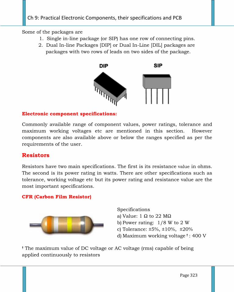
Ch 9: Practical Electronic Components, their specifications and PCB
Page 323
Some of the packages are
1. Single in-line package (or SIP) has one row of connecting pins.
2. Dual In-line Packages [DIP] or Dual In-Line [DIL] packages are
packages with two rows of leads on two sides of the package.
Electronic component specifications:
Commonly available range of component values, power ratings, tolerance and
maximum working voltages etc are mentioned in this section. However
components are also available above or below the ranges specified as per the
requirements of the user.
Resistors
Resistors have two main specifications. The first is its resistance value in ohms.
The second is its power rating in watts. There are other specifications such as
tolerance, working voltage etc but its power rating and resistance value are the
most important specifications.
CFR (Carbon Film Resistor)
† The maximum value of DC voltage or AC voltage (rms) capable of being
applied continuously to resistors
Specifications
a) Value: 1 Ω to 22 MΩ
b) Power rating: 1/8 W to 2 W
c) Tolerance: ±5%, ±10%, ±20%
d) Maximum working voltage † : 400 V
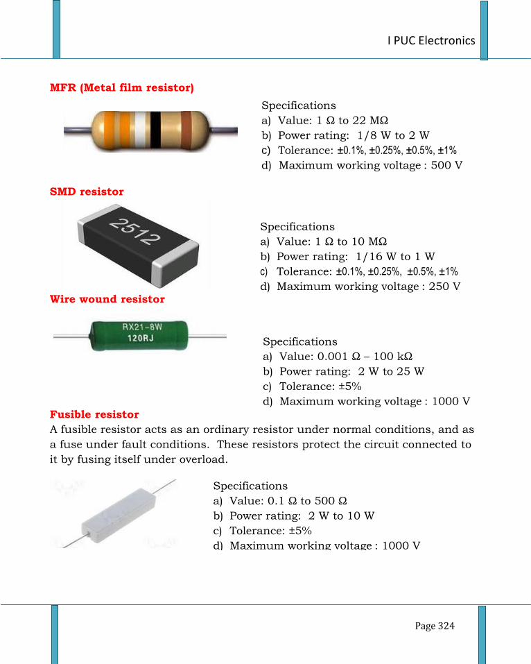
I PUC Electronics
Page 324
MFR (Metal film resistor)
SMD resistor
Wire wound resistor
Fusible resistor
A fusible resistor acts as an ordinary resistor under normal conditions, and as
a fuse under fault conditions. These resistors protect the circuit connected to
it by fusing itself under overload.
Specifications
a) Value: 0.1 Ω to 500 Ω
b) Power rating: 2 W to 10 W
c) Tolerance: ±5%
d) Maximum working voltage : 1000 V
Specifications
a) Value: 1 Ω to 22 MΩ
b) Power rating: 1/8 W to 2 W
c) Tolerance: ±0.1%, ±0.25%, ±0.5%, ±1%
d) Maximum working voltage : 500 V
Specifications
a) Value: 1 Ω to 10 MΩ
b) Power rating: 1/16 W to 1 W
c) Tolerance: ±0.1%, ±0.25%, ±0.5%, ±1%
d) Maximum working voltage : 250 V
Specifications
a) Value: 0.001 Ω – 100 kΩ
b) Power rating: 2 W to 25 W
c) Tolerance: ±5%
d) Maximum working voltage : 1000 V
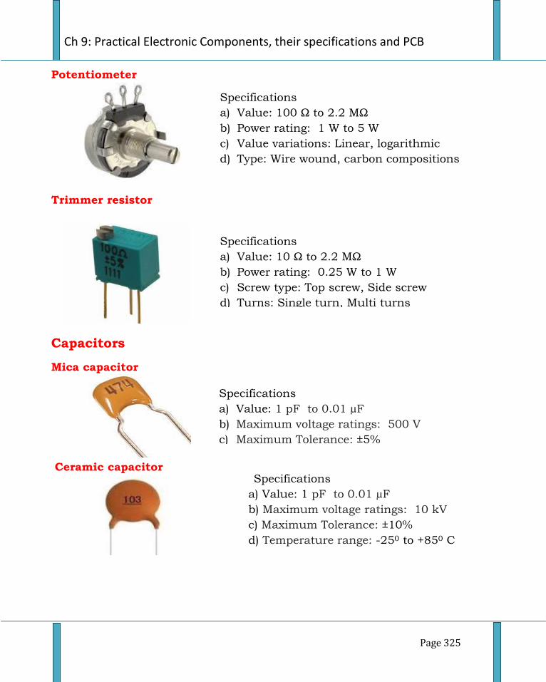
Ch 9: Practical Electronic Components, their specifications and PCB
Page 325
Potentiometer
Trimmer resistor
Capacitors
Mica capacitor
Ceramic capacitor
Specifications
a) Value: 1 pF to 0.01 µF
b) Maximum voltage ratings: 500 V
c) Maximum Tolerance: ±5%
Specifications
a) Value: 100 Ω to 2.2 MΩ
b) Power rating: 1 W to 5 W
c) Value variations: Linear, logarithmic
d) Type: Wire wound, carbon compositions
Specifications
a) Value: 10 Ω to 2.2 MΩ
b) Power rating: 0.25 W to 1 W
c) Screw type: Top screw, Side screw
d) Turns: Single turn, Multi turns
Specifications
a) Value: 1 pF to 0.01 µF
b) Maximum voltage ratings: 10 kV
c) Maximum Tolerance: ±10%
d) Temperature range: -250 to +850 C
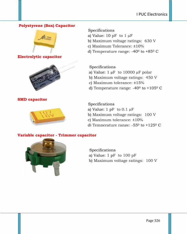
I PUC Electronics
Page 326
Polystyrene (Box) Capacitor
Electrolytic capacitor
SMD capacitor
Variable capacitor - Trimmer capacitor
Specifications
a) Value: 10 pF to 1 µF
b) Maximum voltage ratings: 630 V
c) Maximum Tolerance: ±10%
d) Temperature range: -400 to +850 C
Specifications
a) Value: 1 pF to 100 pF
b) Maximum voltage ratings: 100 V
Specifications
a) Value: 1 µF to 10000 µF polar
b) Maximum voltage ratings: 450 V
c) Maximum tolerance: ±15%
d) Temperature range: -400 to +1050 C
Specifications
a) Value: 1 pF to 0.1 µF
b) Maximum voltage ratings: 100 V
c) Maximum tolerance: ±10%
d) Temperature range: -550 to +1250 C
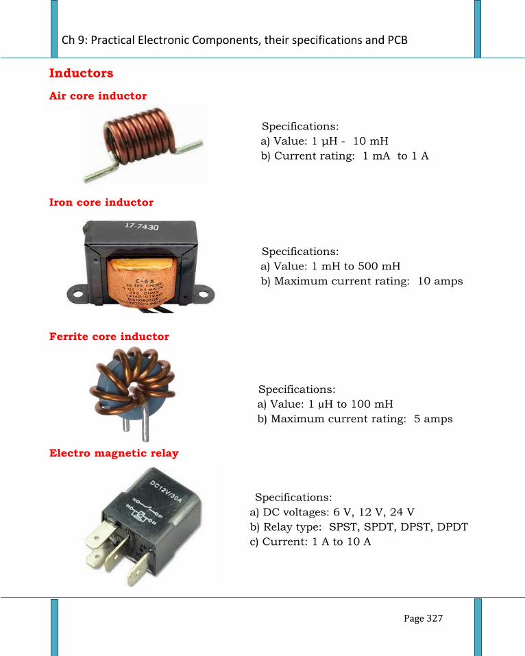
Ch 9: Practical Electronic Components, their specifications and PCB
Page 327
Inductors
Air core inductor
Iron core inductor
Ferrite core inductor
Electro magnetic relay
Specifications:
a) Value: 1 μH - 10 mH
b) Current rating: 1 mA to 1 A
Specifications:
a) Value: 1 mH to 500 mH
b) Maximum current rating: 10 amps
Specifications:
a) Value: 1 µH to 100 mH
b) Maximum current rating: 5 amps
Specifications:
a) DC voltages: 6 V, 12 V, 24 V
b) Relay type: SPST, SPDT, DPST, DPDT
c) Current: 1 A to 10 A
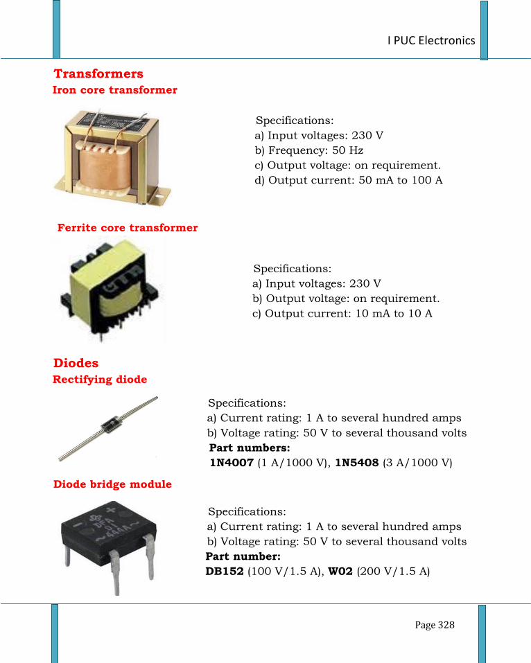
I PUC Electronics
Page 328
Transformers
Iron core transformer
Ferrite core transformer
Diodes
Rectifying diode
Diode bridge module
Specifications:
a) Input voltages: 230 V
b) Frequency: 50 Hz
c) Output voltage: on requirement.
d) Output current: 50 mA to 100 A
Specifications:
a) Input voltages: 230 V
b) Output voltage: on requirement.
c) Output current: 10 mA to 10 A
Specifications:
a) Current rating: 1 A to several hundred amps
b) Voltage rating: 50 V to several thousand volts
Part numbers:
1N4007 (1 A/1000 V), 1N5408 (3 A/1000 V)
Specifications:
a) Current rating: 1 A to several hundred amps
b) Voltage rating: 50 V to several thousand volts
Part number:
DB152 (100 V/1.5 A), W02 (200 V/1.5 A)
)
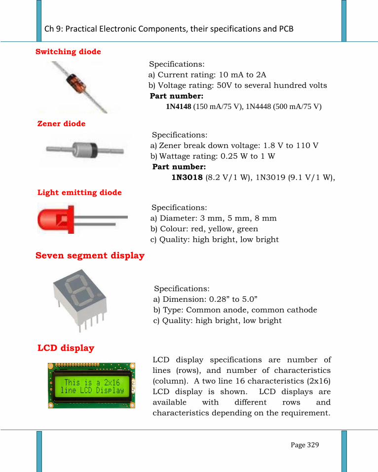
Ch 9: Practical Electronic Components, their specifications and PCB
Page 329
Switching diode
Zener diode
Light emitting diode
Seven segment display
LCD display
Specifications:
a) Current rating: 10 mA to 2A
b) Voltage rating: 50V to several hundred volts
Part number:
1N4148 (150 mA/75 V), 1N4448 (500 mA/75 V)
Specifications:
a) Zener break down voltage: 1.8 V to 110 V
b) Wattage rating: 0.25 W to 1 W
Part number:
1N3018 (8.2 V/1 W), 1N3019 (9.1 V/1 W),
Specifications:
a) Diameter: 3 mm, 5 mm, 8 mm
b) Colour: red, yellow, green
c) Quality: high bright, low bright
Specifications:
a) Dimension: 0.28” to 5.0”
b) Type: Common anode, common cathode
c) Quality: high bright, low bright
LCD display specifications are number of
lines (rows), and number of characteristics
(column). A two line 16 characteristics (2x16)
LCD display is shown. LCD displays are
available with different rows and
characteristics depending on the requirement.
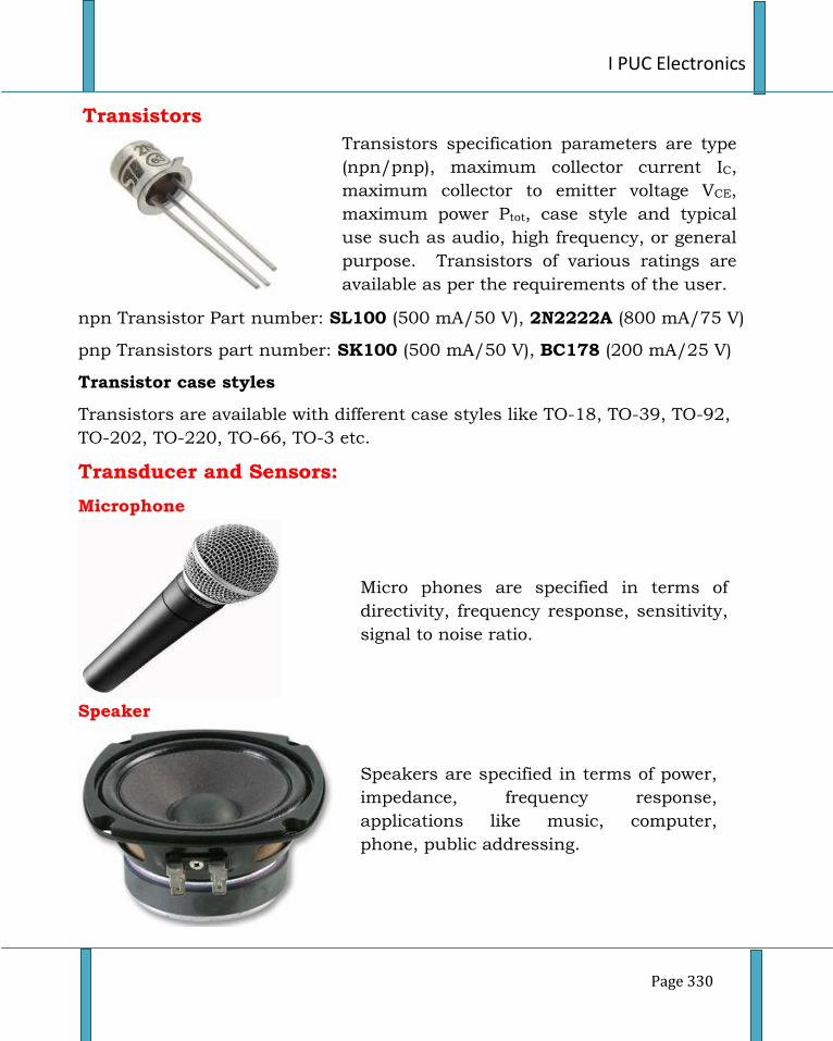
I PUC Electronics
Page 330
Transistors
npn Transistor Part number: SL100 (500 mA/50 V), 2N2222A (800 mA/75 V)
pnp Transistors part number: SK100 (500 mA/50 V), BC178 (200 mA/25 V)
Transistor case styles
Transistors are available with different case styles like TO-18, TO-39, TO-92,
TO-202, TO-220, TO-66, TO-3 etc.
Transducer and Sensors:
Microphone
Speaker
Transistors specification parameters are type
(npn/pnp), maximum collector current IC,
maximum collector to emitter voltage VCE,
maximum power Ptot, case style and typical
use such as audio, high frequency, or general
purpose. Transistors of various ratings are
available as per the requirements of the user.
Micro phones are specified in terms of
directivity, frequency response, sensitivity,
signal to noise ratio.
Speakers are specified in terms of power,
impedance, frequency response,
applications like music, computer,
phone, public addressing.
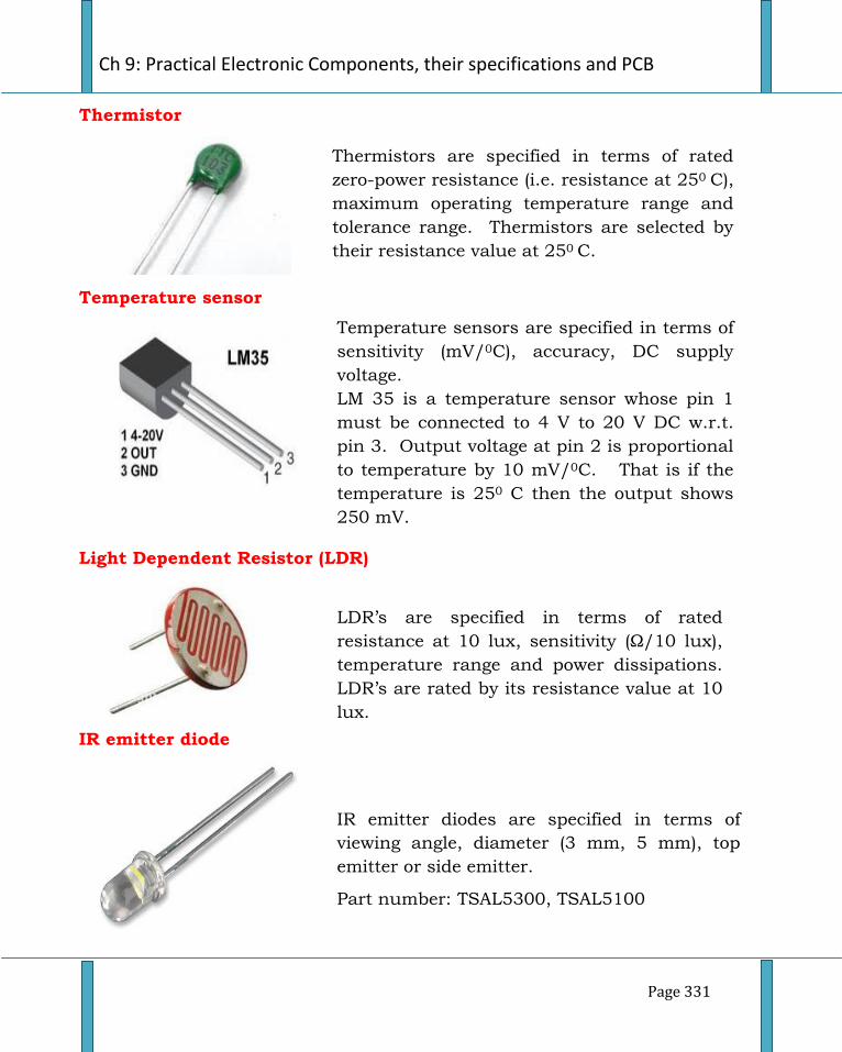
Ch 9: Practical Electronic Components, their specifications and PCB
Page 331
Thermistor
Temperature sensor
Light Dependent Resistor (LDR)
IR emitter diode
LDR’s are specified in terms of rated
resistance at 10 lux, sensitivity (Ω/10 lux),
temperature range and power dissipations.
LDR’s are rated by its resistance value at 10
lux.
Temperature sensors are specified in terms of
sensitivity (mV/0C), accuracy, DC supply
voltage.
LM 35 is a temperature sensor whose pin 1
must be connected to 4 V to 20 V DC w.r.t.
pin 3. Output voltage at pin 2 is proportional
to temperature by 10 mV/0C. That is if the
temperature is 250 C then the output shows
250 mV.
Thermistors are specified in terms of rated
zero-power resistance (i.e. resistance at 250 C),
maximum operating temperature range and
tolerance range. Thermistors are selected by
their resistance value at 250 C.
IR emitter diodes are specified in terms of
viewing angle, diameter (3 mm, 5 mm), top
emitter or side emitter.
Part number: TSAL5300, TSAL5100
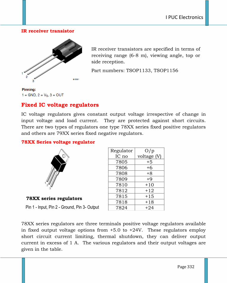
I PUC Electronics
Page 332
IR receiver transistor
Fixed IC voltage regulators
IC voltage regulators gives constant output voltage irrespective of change in
input voltage and load current. They are protected against short circuits.
There are two types of regulators one type 78XX series fixed positive regulators
and others are 79XX series fixed negative regulators.
78XX Series voltage regulator
78XX series regulators
Pin 1 - Input, Pin 2 - Ground, Pin 3- Output
78XX series regulators are three terminals positive voltage regulators available
in fixed output voltage options from +5.0 to +24V. These regulators employ
short circuit current limiting, thermal shutdown, they can deliver output
current in excess of 1 A. The various regulators and their output voltages are
given in the table.
Regulator
IC no
O/p
voltage (V)
7805 +5
7806 +6
7808 +8
7809 +9
7810 +10
7812 +12
7815 +15
7818 +18
7824 +24
IR receiver transistors are specified in terms of
receiving range (6-8 m), viewing angle, top or
side reception.
Part numbers: TSOP1133, TSOP1156
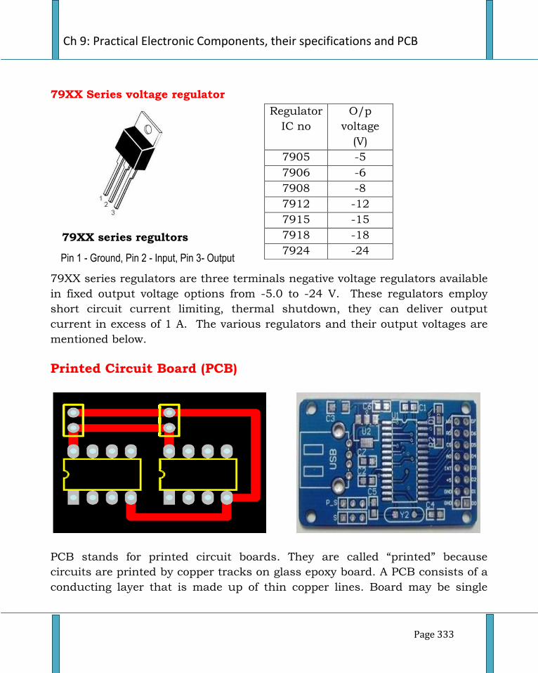
Ch 9: Practical Electronic Components, their specifications and PCB
Page 333
79XX Series voltage regulator
79XX series regultors
Pin 1 - Ground, Pin 2 - Input, Pin 3- Output
79XX series regulators are three terminals negative voltage regulators available
in fixed output voltage options from -5.0 to -24 V. These regulators employ
short circuit current limiting, thermal shutdown, they can deliver output
current in excess of 1 A. The various regulators and their output voltages are
mentioned below.
Printed Circuit Board (PCB)
PCB stands for printed circuit boards. They are called “printed” because
circuits are printed by copper tracks on glass epoxy board. A PCB consists of a
conducting layer that is made up of thin copper lines. Board may be single
Regulator
IC no
O/p
voltage
(V)
7905 -5
7906 -6
7908 -8
7912 -12
7915 -15
7918 -18
7924 -24
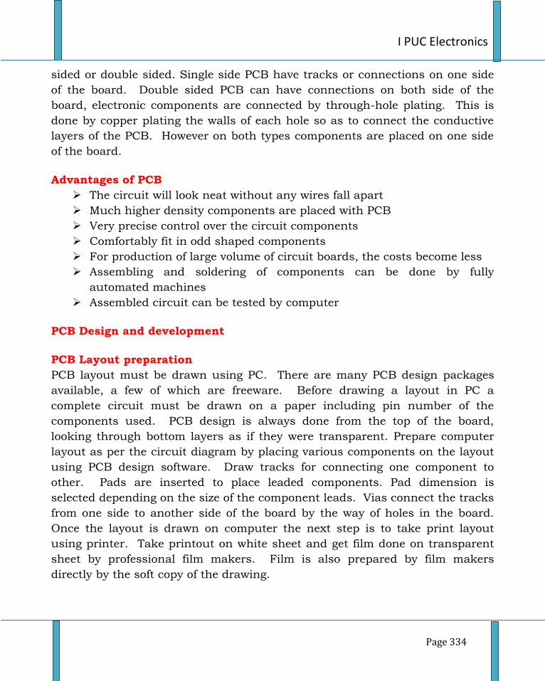
I PUC Electronics
Page 334
sided or double sided. Single side PCB have tracks or connections on one side
of the board. Double sided PCB can have connections on both side of the
board, electronic components are connected by through-hole plating. This is
done by copper plating the walls of each hole so as to connect the conductive
layers of the PCB. However on both types components are placed on one side
of the board.
Advantages of PCB
The circuit will look neat without any wires fall apart
Much higher density components are placed with PCB
Very precise control over the circuit components
Comfortably fit in odd shaped components
For production of large volume of circuit boards, the costs become less
Assembling and soldering of components can be done by fully
automated machines
Assembled circuit can be tested by computer
PCB Design and development
PCB Layout preparation
PCB layout must be drawn using PC. There are many PCB design packages
available, a few of which are freeware. Before drawing a layout in PC a
complete circuit must be drawn on a paper including pin number of the
components used. PCB design is always done from the top of the board,
looking through bottom layers as if they were transparent. Prepare computer
layout as per the circuit diagram by placing various components on the layout
using PCB design software. Draw tracks for connecting one component to
other. Pads are inserted to place leaded components. Pad dimension is
selected depending on the size of the component leads. Vias connect the tracks
from one side to another side of the board by the way of holes in the board.
Once the layout is drawn on computer the next step is to take print layout
using printer. Take printout on white sheet and get film done on transparent
sheet by professional film makers. Film is also prepared by film makers
directly by the soft copy of the drawing.
Ch 9: Practical Electronic Components, their specifications and PCB
Page 335
Photo-resist
Film (phot-resist) or mask is placed on copper-clad board. UV light is exposed
on copper clad board covered by photo-resist film. UV light does not pass
through photo-resists i.e. on the tracks, pads etc. Copper area which is not
protected by photo-resist is removed during etching process.
PCB Etching Process
All PCB’s are made by bonding a layer of copper over the entire substrate,
sometimes on both sides. Etching process has to be done to remove the
unnecessary copper after UV exposure, leaving behind only the desired copper
tracks. Though there are many methods available for etching, the most
common method used is etching by ferric chloride or hydrochloric acid. Dip
the PCB inside the solution and keep it moving inside. Take it out at times and
stop the process as soon as the unwanted copper has gone. After etching, rub
the PCB with a little acetone to remove the black colour, thus giving the PCB a
shining attractive look. The PCB layout is now complete.
PCB Drilling
The components to be attached to the multi-layered PCB can be done only by
vias drilling. That is, a through hole is drilled in the shape of annular rings.
Small drill bits are used for the drilling. Usually, a 0.8mm drill bit is used. For
high volume production automated drilling machines are used.
Conductor Plating
The layer of the PCB contains copper connections which may not allow good
solderability of the components. To make it good solderable, the surface of the
material has to be plated with tin, or nickel.
PCB Assembling
PCB assembling includes the assembling of the electronic components on to
the respective holes in the PCB. This can be done by through-hole construction
or surface-mount construction. In the former method, the component leads are
inserted into the holes drilled in the PCB. In the latter method, a pad having
the legs similar to the PCB design is inserted and the IC’s are placed or fixed on
top of them. The common aspect in both the methods is that the component
leads are electrically and mechanically fixed to the board with a solder.
I PUC Electronics
Page 336
Questions
One Mark questions
1. What is a part number?
2. Mention the important specifications of a resistor.
3. For what application fusible resisters are used?
4. What is the important specification of a capacitor?
5. Name the type of capacitor having polarity.
6. Write a part number for a diode.
7. How many pins presents in a diode bridge.
8. Mention any one type of seven segment display.
9. What do we mean 16x2 LCD?
10. Mention one specification of a speaker.
11. Mention a part number of a commonly used temperature sensor?
12. Mention any one case style of transistor.
13. Mention any one part number of a positive voltage regulator?
14. Mention any one part number of a negative fixed voltage regulator?
15. Name the chemicals used for Etching process in PCB designing?
Two Mark questions
1. What do you mean by data sheet?
2. What do we understand by part number of an electronic component?
3. What information does a package details of a component give?
4. What do you mean SIP and DIP packages?
5. Write the any two specification of a transformer.
6. Mention any two types of relays available in the market.
7. Mention any two types of transistors case styles available in market.
8. Write any two specifications of LEDs.
9. Write any one part number for npn and pnp transistors.
10.What is etching process?
Three/Five Mark questions
1. List any four advantages of data sheet.
2. Write the step involved in PCB designing.
3. What are the advantages of PCB?


