Molecular Electronics Michael Zwolak and Massimiliano Di Ventra Department of Physics, Virginia Polytechnic Institute and State University, Blacksburg, Virginia 24061-0435 (Dated: March 2003) 1
Transcript
Molecular Electronics
Michael Zwolak and Massimiliano Di Ventra
Department of Physics, Virginia Polytechnic Institute
and State University, Blacksburg, Virginia 24061-0435
(Dated: March 2003)
1
As discussed in the previous chapter, the limits of silicon-based computer technology
(microelectronics) are fast approaching. Alternative technologies are thus being investigated.
Molecular electronics is one of these alternatives. Molecular electronics can be loosely defined
as a subfield of nanotechnology that envisions the use of single molecules, or small groups of
molecules, as components in electronics applications. Along this line, molecular electronic
devices could form the next generation of transistors, sensors, and circuits. Molecules can
have feature lengths as small as 1 nm, making it possible to extend the validity of Moore’s
law for many years to come, should we be able to integrate them into circuits. In addition,
although the envisioned operation of many molecular devices mimics traditional devices, the
quantum world can open up novel possibilities for the way devices work.
The idea of using molecules as components in electronics was suggested more than two
decades ago.1 However, it is only in the last decade that we have witnessed an increased
interest in the field. This is partly due to both our growing ability to fabricate contacts with
nanometer size, which can accommodate a small number of molecules in between them, and
the development of self-assembly. The methods used in making these prototype devices are,
however, often difficult to control and, as of now, not quite ready to make the necessary
step into commercialization. Nevertheless, the field of molecular electronics is experiencing
tremendous growth, with new ideas being generated at an amazing rate.
This chapter will provide a limited overview of the field, not a review. This simply
means that we will select a few examples from the literature and discuss them in the broader
context of the physical phenomena we observe at the nanoscale. In particular, we will discuss
ways to assemble and probe molecular devices, report on their electrical characteristics, and
outline the various factors that influence their properties. We will also discuss possible charge
2
transport mechanisms in these devices, and finally we will outline integration strategies and
related difficulties associated with working at such small length scales. Our focus will be
on the transport properties of organic molecules and small fullerenes. We will also briefly
discuss the possibility of using DNA in electronics. Nanotube-based electronic devices and
their transport properties have been covered in the previous chapter and in Chapter 6.
I. TOOLS AND WAYS TO BUILD AND PROBE MOLECULAR DEVICES
Two ingredients are necessary to make a molecular device: an aperture of nanoscale
dimensions and a way to arrange one or more molecules within it. Two main methods
have been used in recent years to make nanoscale apertures: the break-junction technique2
and electromigration.3 Combined with the property of certain molecules to self-assemble on
metallic surfaces, these two methods can, in principle, be used to create single-molecule
nanojunctions. Self-assembly has been discussed at length in Chapter 2. We just recall that
its basic principle is to exploit chemical interactions to create a structure on the nanoscale.
In the context of molecular electronics, an example of such an interaction is the binding of
a thiol group (— S –H ) with a gold surface. The use of a Scanning Tunneling Microscope
(STM) to probe the conductance of molecules self-assembled on a metal surface will be
discussed later on in this section.
A. Break-junction technique
A break-junction is formed by literally breaking a thin metal wire to form a very small
gap in the wire, in which a molecule or a group of molecules can be placed. This method was
3
developed in the late 1980’s and early 1990’s.4 Typically, a thin metal wire is fabricated using
standard techniques like optical or e-beam lithography (see Chapter 1), on top of a flexible
substrate, e.g., polyimide. A thin wire can also be attached to the substrate by gluing it
on using an epoxy. A sharp object (or e-beam lithography) is then used to notch the wire.
The wire is subsequently broken at the point of the notch by bending the substrate, which,
due to its flexibility, will remain intact. The bending is then slightly relaxed to bring the
two parts of the wire back into contact. A piezoelectric actuator is used to both break the
wire and to adjust the width of the gap between the two parts of the broken wire. The
piezoelectric actuator uses a piezoelectric material, typically a ceramic, to precisely adjust
the distance between the two wires. A piezoelectric material deforms under application of an
external voltage. This material is placed below the substrate, and when it expands, it bends
the substrate. The more the substrate is bent, the larger the gap between the two wires.
A typical experimental setup is shown in Figure 10.1. This is the so-called mechanically
controllable break-junction.
There are several major advantages to the break-junction technique. It works in a range
of conditions from ambient to low temperature/high vacuum, and in conjunction with other
experimental setups. It also has a relatively high experimental “success rate,” in the sense
that the formed nanojunction can be reproduced fairly well. Additionally, since the substrate
is bent to adjust the size of the electrode gap, only small fluctuations in the gap size are
expected. This is because the size of the electrode gap changes by a lower amount than
the amount of expansion of the piezoelectric element (called the reduction factor) due to the
setup geometry. In this way, the effects of fluctuations in the piezoelectric element expansion
are reduced. This allows for accurate control of the size of the electrode gap.
4
Figure 10.1: Experimental setup of a mechanically controllable break-junction with (a) the flexible
substrate, (b) the counter supports, (c) the notched wire, (d) the glue contacts, (e) the piezoelectric
element, and (f) the solution containing the molecule of interest. (From Ref. 2 by permission of
the American Association for the Advancement of Science.)
The conductance of benzene-1,4-dithiolate molecules was first measured using this tech-
nique.2 In this experiment, a notched gold wire was glued onto a substrate. Benzene-1,4-
dithiol molecules were self-assembled onto the gold surface via adsorption of the thiol group
on the gold surface to form a self-assembled monolayer (SAM). The gold wire was then bro-
ken in the solution, which causes the SAM formation around the two newly formed gold tips
(note that by “tip” we do not necessarily mean a single atom termination of the wire). The
solution was subsequently evaporated, and the two sides of the wire were brought together
until conduction was observed. This is thought to be the point when a single molecule
bridges the two gold tips. The spacing of the two gold tips was estimated to be about 0.8
nm, i.e., enough to accommodate a benzene-1,4-dithiolate molecule. A schematic of the
break-junction used in this experiment is shown in Figure 10.2. The results of the exper-
iment are discussed below in Section II. We just note here that even though the spacing
of the nanojunction can be controlled with some accuracy, it is not at all clear how many
5
Figure 10.2: Schematic of a break-junction with a SAM of benzene-1,4-dithiol molecules. (From
Ref. 2 by permission of the American Association for the Advancement of Science.)
molecules bridge the gap and what the actual bonding configuration is to the gold tips.
B. Forming nanogaps with electromigration
An alternative way of creating nanoscale junctions is by using a physical phenomenon
known as electromigration. Electrons diffusing in a conductor can scatter atoms away from
their equilibrium position. If the electric current density is large enough, i.e., if a lot of these
scattering events takes place, the atoms can be moved along the conductor, leaving holes of
missing atoms behind. Electromigration is still a major concern in microelectronics since it
is the major failure mechanism in solid-state circuits. However, in the context of molecular
electronics it can be used advantageously.5 A nanowire is first made using e-beam lithography.
6
Figure 10.3: SEM image of a gold wire (a) before and (b) after break-up by electromigration. (From
Ref. 5 by permission of the American Institute of Physics.)
A nanometer-size gap is then created by controlling the amount of current that passes in
the wire. While increasing the current, the conductance of the wire is monitored with a
voltage probe. For small current values, the conductance of the wire remains unaffected.
With further increase of the current, however, a change in the resistance is observed that
indicates the onset of electromigration. By increasing the current further, the conductance
eventually drops almost to zero, indicating a gap has formed. The width of this gap is
estimated to be about 1 nm from the value of the tunneling resistance between the two newly
formed electrodes. The process seems to be highly reproducible as long as the diameter of
the wire is a few nanometers.5 Figure 10.3 shows a Scanning Electron Microscope (SEM)
image of a gold wire before [Figure 10.3(a)] and after [Figure 10.3(b)] the break-up process
due to electromigration. This technique can be combined with self-assembly to create a
molecular junction in a similar manner to the break-junction technique. As in the case of
the mechanically controllable break-junction, it is uncertain how many molecules bridge the
nanogap and what the bonding configuration is.
7
C. Probing individual molecules
Information on the transport properties of molecules can also be obtained using a Scanning
Tunneling Microscope (STM) [see Chapter 3]. The molecules are first self-assembled on a
metal surface and then the STM tip is used as a second contact. This is schematically shown
in Figure 10.4, where a single molecule is shown between an STM tip and an electrode
surface.
As discussed in Chapter 3, the operation of the STM relies on what is called the tunneling
current, i.e., on the fact that a particle can penetrate into a classically forbidden energy
region. In Figure 10.4, the tunneling current flows between the tip and the SAM to be
scanned when the tip is sufficiently close to the sample (a distance generally less than 1
nm). The tip is moved toward the surface similarly to the way the break-junction gap is
adjusted: a piezoelectric element, to which a voltage is applied, is used to adjust the tip
height until the current flows. The whole sample can be scanned by, for instance, changing
the tip height in order to keep a constant tunneling current, in this way obtaining a map
of the surface height (surface topography). To measure the conductance of single molecules,
the feedback loop, which adjusts the height of the STM, is shut off. This keeps the tip at
a constant position while measuring the current-voltage (I-V) characteristics, i.e., changing
the external voltage and recording the current through the sample. It is important to note
that the measured conductance can correspond to a small group of molecules, not necessarily
to a single one. Another way to measure the I-V characteristics of the sample is to use an
alternating current STM. By applying an alternating voltage across the tip and the metal
surface, a frequency-dependent current can be measured.
Using an STM to measure the I-V characteristics of molecules has actually been one of the
8
Figure 10.4: Schematic of a SAM used to prop up a single molecule so that charge transport along
the length of the molecule can be probed using an STM. (From Ref. 7 by permission of the Institute
of Electrical and Electronics Engineers.)
first methods to obtain information on their transport properties. However, this approach
has some limitations. The magnitude of the current can strongly depend on the tunneling
barrier between the STM tip and the molecule, introducing an additional and undesirable
“contact” resistance. This can be partly corrected for by, e.g., adding a thiol group to the end
of the molecule and then attaching it to a gold nanoparticle.6 The nanoparticle can then make
contact with the STM tip. However, this introduces additional uncertainties in the current
due to the particle size and how well it is contacted to the STM tip. Another disadvantage
is that it is unlikely that lone molecules will be perpendicularly aligned to the surface. A
possible solution to this problem is to use an SAM of “insulating” molecules to prop up the
small group of “conducting” molecules that need to be probed, as shown in Figure 10.4.7
Here we call “insulating” a particular molecule whose resistance has been measured to be
9
much larger than the molecule of interest in a similar experimental set-up. For instance, an
alkanethiol can be used to form the support SAM, while π-conjugated molecules (which must
be longer so they stick out far from the support SAM and can be located by the STM) are
deposited afterward.8 It has been shown that the molecules of interest will insert into defect
regions in the support SAM. These are regions where the directionality of the molecules in
the SAM change. In this way, the molecules of interest will be propped up by the SAM and
located by the STM, and then their conductance can be measured.
Similarly, the conductance of single molecules or small groups of molecules can be mea-
sured by using an Atomic Force Microscope (AFM) [see Chapter 1]. Here, a tip is held at
the end of a cantilever (or arm). The tip is dragged across the sample (or the sample moved)
using a piezoelectric element. The tip will move up and down with the height of the local
area of the sample. Generally, a laser beam is reflected off the back of the cantilever, and
a multi-segment photodiode detects the movement of the beam. There are two modes that
the AFM can be run in, either a mode with no gain or a mode with high gain (constant
force). In the former, the tip is just dragged across the sample, but the cantilever will bend
and exert additional force where the sample is higher. As long as this is calibrated for, then
the surface can be scanned and the height extracted. In high gain mode, either the sample
height or cantilever height is adjusted so that there is no additional bending of the cantilever,
which gives a constant force. The measurement of the conductance of a SAM with an AFM
(conducting probe AFM) can be done by applying a voltage across the cantilever (and tip)
and the electrode on which the sample is assembled.
10
II. CONDUCTANCE MEASUREMENTS
In the previous section, we discussed ways to measure and probe the I-V characteristics
of individual molecules or small groups of molecules. We are now ready to discuss some of
the measurements reported in literature. Instead of reviewing all measurements done so far
(which is beyond the scope of this chapter), we will select a few that show different features.
This will allow us to introduce the different transport mechanisms that are believed to occur
in these systems. The reader is warned that the field is rapidly changing, with experiments
being performed in an increasingly controlled manner. Many of the physical interpretations
we report can therefore change in the near future.
A. Contact resistance vs. quantized conductance
A prototype molecular device that has received much attention both experimentally and
theoretically is one formed by a benzene-1,4-dithiol molecule between two gold electrodes.
In the previous section, we discussed how this device can be made using self-assembly and a
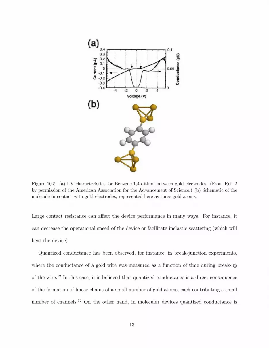
mechanically controllable break-junction. The I-V characteristics of this device are shown in
Fig 10.5(a) and a schematic of its possible atomic configuration in Fig 10.5(b). It is assumed
that the hydrogens of the thiol groups (— S –H ) at each end of the molecule desorb and
the sulfur atoms bind strongly to the surface of the two gold tips. The I-V characteristics
show nonlinear behavior with peaks and valleys in the conductance as a function of bias.
A molecule like this has several electronic states that are filled with electrons up to the
highest occupied molecular orbital (HOMO), which is a few electron volts below the lowest
unoccupied molecular orbital (LUMO). When the molecule makes contact with the gold
11
electrodes these states broaden and the Fermi level lies between the HOMO and the LUMO
[see Figure 10.6(a)]. By increasing the bias, one of the electronic states of the molecule can
align with the left or right chemical potentials giving rise to a peak in the conductance [see
Figure 10.6(b)]. This phenomenon is known as “resonant tunneling” and has been invoked to
explain the peaks and valleys observed in this experiment.9,10 Negative differential resistance,
a phenomenon also associated with resonant tunneling (see below), was not observed in this
experiment. What theory has not been able to explain yet is the large resistance observed
in this and many other experiments with organic molecules. This brings us to the question
of what actually determines the resistance in a nanoscale junction.
The electrodes have many current-carrying modes (essentially infinite), while the junction,
specifically the molecule, has only a few. Thus, as current flows from one electrode into
the junction, it must redistribute itself into the fewer modes available. This redistribution
introduces a contact resistance which is inversely proportional to the number of modes in the
junction and inversely proportional to the probability per mode that an electron can cross
the junction (transmission probability). The larger the number of modes in the junction,
the less resistance this redistribution will introduce. If only one mode is accessible in the
junction and its transmission probability is one, then a conductance (inverse of resistance)
of 2e2/h should be observed, where e is the electron charge and h is Planck’s constant. This
phenomenon is referred to as quantized conductance, and implies that even an ideal wire will
show quite a large resistance of ∼12.9 kΩ. This resistance is due to the contact resistance
associated with each mode. That is, the resistance is not in the wire itself, but is instead
associated with redistribution of the current carrying modes in the contact where it connects
to the conductor (for a more extensive discussion the reader is encouraged to look at Ref. 11).
12
Figure 10.5: (a) I-V characteristics for Benzene-1,4-dithiol between gold electrodes. (From Ref. 2
by permission of the American Association for the Advancement of Science.) (b) Schematic of the
molecule in contact with gold electrodes, represented here as three gold atoms.
Large contact resistance can affect the device performance in many ways. For instance, it
can decrease the operational speed of the device or facilitate inelastic scattering (which will
heat the device).
Quantized conductance has been observed, for instance, in break-junction experiments,
where the conductance of a gold wire was measured as a function of time during break-up
of the wire.12 In this case, it is believed that quantized conductance is a direct consequence
of the formation of linear chains of a small number of gold atoms, each contributing a small
number of channels.12 On the other hand, in molecular devices quantized conductance is
13
µL
ELUMO
EHOMO
µL
EHOMO
ELUMO
µR
µR
(b)
(a) E
z
E
zV
Figure 10.6: (a) Schematic of the energy configuration of a molecular junction with the Fermi level
located in the HOMO-LUMO gap of the molecule. The HOMO and LUMO states are depicted as
broadened energy levels due to their interaction with the electrodes. (b) As the voltage is increased,
eventually the HOMO or LUMO will align with the Fermi level of the right or left electrode. This
will cause an increase in the magnitude of the current.
rarely observed. Actually, their resistance is quite large. This can be explained as follows.
The number of channels accessible at zero temperature is determined by the number of
states with energies between the Fermi levels of the two electrodes. When the molecule
is in contact with the electrodes there is generally only a small amount (density) of states
between the HOMO and the LUMO, which is due to the presence of the electrodes. Thus,
the molecule offers a large resistance to current flow. The amount of resistance in molecular
junctions is linked to the amount of overlap between the electronic states of the molecule
and the conduction states in the bulk electrodes. This overlap determines the probability
that an electron can actually transmit across the molecule. Poor overlap can be caused by,
e.g., the spatial distribution of the molecular orbitals or by poor physical contact (like in
STM experiments), which causes the electronic states of the electrode and the molecule to
14
be spatially separated.
The resistance due to poor overlap of electronic states is well illustrated by the break-
junction experiment with benzene-1,4-dithiolate molecules. A possible atomic configuration
of this system is the one depicted in Fig 10.5(b). If this is the case, the sulfur atoms at
each end of the molecule strongly bind to the two gold electrodes. By strongly we mean
that the energy required to break the sulfur-gold bond is substantial (of the order of few
electron volts). However, the sulfur-gold contact is a poor contact in terms of transmission
probabilities: this contact induces a bad overlap of the electronic states of the molecule
responsible for transport with the conduction states of the electrodes.10 If the contact is
instead, through a single gold atom bound to the sulfur, there is even worse overlap of the
conduction states of the junction and the electrode, which gives an even higher resistance.
That the contact geometry can change the resistance by significant amounts has fostered
an intense debate on the actual atomic configuration of these systems. Theoretical work has
been in fairly good agreement with the experimental results regarding the shape of the I-V
curve but disagrees with the absolute value of the current.9,10,13 Part of this disagreement has
been attributed to the role of the contact geometry in changing the resistance of the junction.
This has been generally true with many of the molecular devices reported in literature. To
better understand this issue we need to recall that molecular devices are generally fabricated
with either mechanically controllable break-junctions or electromigration. Both techniques
yield atomic-scale contacts of unknown geometry: the atomic regions where the molecules
are supposed to bind to the electrodes are not necessarily smooth nor symmetric on opposite
sides of the junction. In addition, the molecules can bind on just one side of the junction
and not the other, or many molecules can bridge the two electrodes allowing current to flow
15
along different paths.14
Recent theoretical reports have also shown that unintentional adsorption of atomic
species, e.g., oxygen, on the electrode surfaces close to (but not necessarily binding to)
the molecule can completely change the I-V characteristics of these devices.15,16 The lat-
ter effect is partly due to the electrostatic interaction between the charge on these species
and the states of the molecular device. Similar effects have been experimentally demon-
strated in carbon nanotube field-effect transistors.17 While these findings show that the I-V
characteristics of molecular devices can be easily tuned (much more than in conventional
microelectronic devices), they also suggest that in order to have reproducible and reliable
operation, atom-by-atom control of their configuration is necessary.
B. Molecular switches, transistors and the like
Despite the above difficulties, several groups have succeeded in making fundamental circuit
elements, like diodes, switches and transistors.2,3,18,19,21,22 Here we give few examples of how
these basic elements can be realized at the molecular level.
A molecular switch is a device which will be activated by an external event to change
its state from “on” to “off”. An electrical switch uses a change in voltage to change a
molecular junction from a conducting state (on) to a non-conducting state (off). A transistor
is somewhat similar, where a gate voltage changes the current from a low to a high value, or
vice versa, but the transistor does not maintain its state.
A molecule that can be used as a switch is shown in Figure 10.7; it is called a catenane.
This molecule changes its internal structure when different voltages are applied across it. For
details on how these structures have been made, the reader is referred to the original papers
16
(see, e.g., Ref. 18 and references therein). Here we just report that the catenanes were first
synthesized and then deposited on a series of polysilicon wires using the Langmuir-Blodgett
technique (see Chapter 2). A second layer of perpendicular wires was deposited on top of
that to form the circuit. The current through the device was measured by applying a series of
high voltage pulses, and then probed with a low applied voltage after each pulse. Hysteresis
was observed in the current-voltage characteristics (see Figure 10.8), which means that the
current assumes a different value when it is scanned by increasing the magnitude of voltage
pulses compared to decreasing the magnitude of voltage pulses. Hysteresis is necessary in
devices like computer memory.
A possible mechanism for such a behavior is what has been called ”mechanochemistry“.
This mechanism is shown in Figure 10.7. The catenane has two states: “open” ([A0]) and
“closed” ([B0]). The “open” state being a high current state and “closed” being a low current
state. Application of a positive voltage brings [A0] to the state [A+] which will rearrange
due to repulsion of the positive charge on the two rings. When the voltage is decreased, this
will bring the catenane to the closed state [B0]. The catenane can be brought back to the
[A0] state by the application of a negative voltage. Similar results have been reported with
other molecules, like rotaxanes (see, e.g., Ref. 18).
One of the most important elements in microelectronics is the field-effect transistor (FET).
Using nanotubes to make FETs has been described in the previous chapter and in Chapter 6.
Single-electron transistors made with quantum dots will be discussed in the following chapter.
Realizing such an element out of single molecules is certainly an important achievement.
However, making an FET from small molecules presents a greater challenge, partly due to
the limits of the fabrication techniques described above, and partly to the difficulty of placing
17
Figure 10.7: Structure of the [2]catenane 34+ is shown in the middle. Mechanochemical mechanism
that is thought to be responsible for the hysteresis observed in the electrical current. This mech-
anism is described in the text. (From Ref. 18 by permission of the American Chemical Society.)
Figure 10.8: Electrical current hysteresis observed in catenane switches. (From Ref. 18 by permis-
sion of the American Chemical Society.)
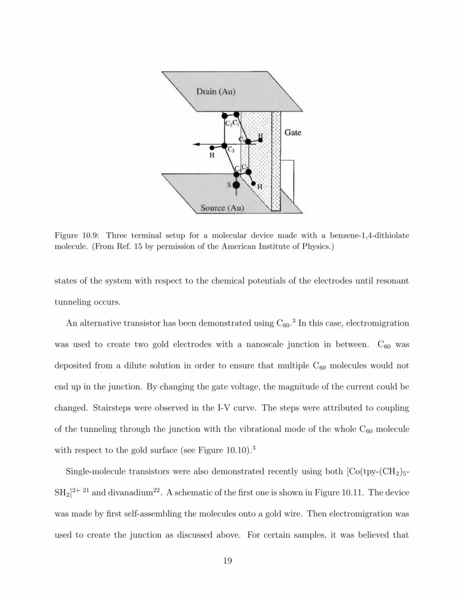
a third terminal in close proximity to the molecules. The prototype benzene-1,4-dithiolate
molecule was one of the first proposals of a molecular FET.20 A possible setup of such device
is shown in Figure 10.9. Here, the molecule plane faces an insulating surface across which a
gate voltage is applied to modulate the current that flows from source to drain. It was found
that source-drain current can be modulated by an order of magnitude by increasing the gate
voltage. The effect of the gate voltage is simply to displace the energy of the electronic
18
Figure 10.9: Three terminal setup for a molecular device made with a benzene-1,4-dithiolate
molecule. (From Ref. 15 by permission of the American Institute of Physics.)
states of the system with respect to the chemical potentials of the electrodes until resonant
tunneling occurs.
An alternative transistor has been demonstrated using C60.3 In this case, electromigration
was used to create two gold electrodes with a nanoscale junction in between. C60 was
deposited from a dilute solution in order to ensure that multiple C60 molecules would not
end up in the junction. By changing the gate voltage, the magnitude of the current could be
changed. Stairsteps were observed in the I-V curve. The steps were attributed to coupling
of the tunneling through the junction with the vibrational mode of the whole C60 molecule
with respect to the gold surface (see Figure 10.10).3
Single-molecule transistors were also demonstrated recently using both [Co(tpy-(CH2)5-
SH2]2+ 21 and divanadium22. A schematic of the first one is shown in Figure 10.11. The device
was made by first self-assembling the molecules onto a gold wire. Then electromigration was
used to create the junction as discussed above. For certain samples, it was believed that
19
Figure 10.10: (a)Schematic drawing of C60 as an oscillator on a gold surface, with an interaction
potential shown on the right. (b) As an electron goes onto C60, the molecule is attracted toward the
surface due the attraction between the electron and its image charge. This gives C60 mechanical
motion. (From Ref. 3 by permission of Nature Publishing Group.)
a single molecule bridged the electrodes. In this case, the current as function of both gate
voltage and applied source-drain voltage displayed characteristics similar to that of single-
electron transistors (see next chapter). Since such characteristics are related to the ability
of the molecule to accommodate single electrons at a time, the cobalt atom is likely to play
a central role in the operation of this device.
C. Electronics with DNA
Charge transport in biological molecules is of interest to several disciplines and is now the
subject of intense research. In particular, DNA and its transport properties have received
much attention in the last decade in view of its possible use in molecular electronics.24,25
Since this topic is increasing in importance and is not covered in any part of this book, we
give here a brief overview of the status of this area.
20
Figure 10.11: (a) Structure of the [Co(tpy-(CH2)5-SH2]2+ and [Co(tpy-SH2]
2+ molecules. (b) Cyclic
voltammogram of [Co(tpy-SH2]2+. (c) I-V curve at different gate voltages for [Co(tpy-(CH2)5-
SH2]2+, the upper inset shows an AFM image of the experimental setup and the lower inset shows
a schematic of the single molecule transistor made with [Co(tpy-(CH2)5-SH2]2+. (From Ref. 21 by
permission of Nature Publishing Group.)
DNA is a double helix formed by a sequence of base pairs with a phosphate-sugar back-
bone. There are four possible bases: thymine, cytosine, adenine, and guanine.
Many experiments have examined the charge transport properties of DNA between elec-
trodes, but there have been seemingly contradictory conclusions. Experiments show DNA
has metallic, semiconducting, insulating, or even superconducting properties. This wide
range of characteristics can be attributed to both the complexity of the DNA structure and
the variety of experimental conditions under which the transport properties of this molecule
can be measured. For example, base sequence, length, orientation, counterions, tempera-
ture, electrode contact, adsorption surface, structure fluctuations, and so on, can all affect
its conducting properties. Therefore, it is still not clear at all how DNA (more precisely, one
21
of its many forms) intrinsically conducts. In some experiments, DNA is believed to conduct
by tunneling of holes between the guanine bases. Guanine has the lowest oxidation poten-
tial, so it is the most favorable place for holes to be located. Between guanines there will
be some sequence of bases that acts as a tunneling barrier. Holes can then tunnel between
the guanine bases, and transverse the length of DNA (see Section III below for details on
transport mechanisms).
DNA is particularly versatile, and even though it might not turn out to have the desired
transport properties for certain applications, it can still be of great use in molecular elec-
tronics. For instance, DNA templated wires have been demonstrated.26 To make these wires,
DNA was used to connect two electrodes and the counterions (which bind along the DNA
backbone to neutralize the negative charge on the phosphate groups) were replaced with ions
of, e.g., silver or gold. Further metal was then deposited along the DNA to create very thin
wires, ten’s of nanometers thick. These wires have been found to conduct very well and could
potentially be used to serve as interconnects in molecular circuits. The fact that DNA could
serve to connect up molecular devices has been shown in recent experimental work, which
used DNA self-assembly to perform molecular lithography.27 Here, a group of researchers
exploited DNA interactions with proteins to selectively metallize (i.e., create a metal wire
around) lengths of DNA. In this way, the researchers were able to create DNA chains that
had a bare DNA region between two metallized regions. This bare region could provide a
location for a molecular device. There are numerous other possibilities to use DNA’s self-
assembly properties to create well structured nanoscale templates. The interested reader
is referred to Ref. 25 for a review on DNA’s possible use in molecular electronics. Also
contained there is an overview of the possible mechanisms by which charge transport could
22
occur in DNA, some of which are reviewed below in a general context.
III. TRANSPORT MECHANISMS AND CURRENT-INDUCED EFFECTS
After outlining the fabrication methods and some of the characteristics of molecular de-
vices, we can now get into more of details of the transport mechanisms and current-induced
effects occurring in these systems. This will give us a better feeling of the physics behind their
operation. We will not be able to discuss all possible mechanisms, in particular those related
to many-body effects (e.g., the Kondo effect), as they would require more advanced knowl-
edge. We refer the reader to the specialized literature for these topics (see, e.g., Ref. 28).
Single-electron tunneling phenomena will be discussed in the next chapter.
A. Resonant tunneling: coherent and sequential
The laws of quantum mechanics allow a particle to overcome a large energy barrier even
if the particle does not have the required energy. This quantum mechanical effect is known
as tunneling. This is schematically shown in Figure 10.12. This effect arises because a
particle is described by a wavefunction, Ψ(x→). The absolute value squared of this function
|Ψ(x→)|2 = Ψ∗(x→)Ψ(x→), i.e., the function times its complex conjugate, gives the probability
that the particle will be found at some position x→. This wavefunction decays exponentially
through an energy barrier (schematically shown in Figure 10.12), such that the probability
that the particle will be found on the other side of the barrier depends on its width and
height.
What we have been considering so far is a particle that can be in any of the (continuum
23
Ψ
E
Figure 10.12: Particle tunneling through an energy barrier. The real part of the right moving
wavefunction Ψ(x) is schematically shown overlaid on top of the energy barrier (note that the
wavefunction is not given in units of energy).
of) states originating from one side of the barrier and ending on the other side. To make
more connection with the experiments described in the previous sections, let us consider
instead a double barrier system, where an electron comes toward the first barrier as a free
particle, tunnels through the barrier into the middle region (quantum well) and eventually
tunnels through the second barrier. In many cases the quantum well can accommodate just
a few (quasi-)discrete states which are available for the electron to be in. The situation
is depicted in Figure 10.13(a), where for simplicity, we show one energy state, ER, in the
junction. If the electron impinges first, say, on the left barrier with energy E not equal to
the discrete state ER in the middle of the junction, the probability that the electron can be
found on the other side of the junction is very small. However, if the electron has an energy
equal to the quantum well energy level ER, then the probability that it can cross the whole
double-barrier junction is high. This is due to enhanced probability that the electron can
be located in the middle of the junction, with a correspondingly higher chance of making it
past the second barrier. In this case, we say that the particle is resonant tunneling through
the junction and a large peak in the current would be observed. If there are multiple energy
levels in the junction, one condition for the peak in the current to be observable is that the
24
levels in the quantum well be far apart compared to the thermal energy kBT . The effect
of the thermal energy is to spread out and lower the absolute value of the peak due to the
smearing out of the electronic distribution which is described by the Fermi function
f(E) =1
exp(E − Ef )/kBT + 1(10.1)
where Ef is the Fermi energy.
To clarify further the phenomenon of resonant tunneling let us step through what happens
when the voltage is increased in the case where there is only one energy level in between the
junction (see Figure 10.13). There is a continuum of states filled up to the chemical potential
in the left electrode µL, and likewise in the right electrode with chemical potential µR. When
no bias is applied (and at zero temperature) there are either no electrons with an energy high
enough to be equal to ER or there are no empty states for electrons to go into at that energy,
the former is shown in Figure 10.13(a). However, when a bias is applied (high voltage on
right side), there will eventually be electrons on the left electrode with energy ER and empty
states on the right electrode for those electrons to tunnel into. An increase in current will be
observed at this point. However, when the bias is increased further, eventually no electrons
will have energy low enough to be in resonance with the energy level in the junction. In this
case, the current decreases (as shown in Figure 10.14). The bias window in which the current
decreases while the voltage increases provides a region with negative differential resistance.
The differential resistance is simply
Rd =
(
∂I
∂V
)−1
(10.2)
25
µL
µL
µR
µL
µR
µR
ER
ER
ER
(a)
(c)
(b) E
E
E
z
z
z
V
V
Figure 10.13: (a) A double energy barrier shown with a (quasi-)discrete state in the junction, which
represents a molecular state. (b) Applying a bias V to the double barrier system causes the (quasi-
)discrete state to line up between filled states in one electrode and empty states in the other. (c)
Increasing V further brings the system out of resonance.
or, in other words, the inverse derivative of the curve in Figure 10.14. There can be resonant
tunneling without a region of negative differential resistance. In this case, only a peak in
conductance, not current, is observed.
26
I
V
Resonant Peak
Figure 10.14: I-V curve with a resonant peak.
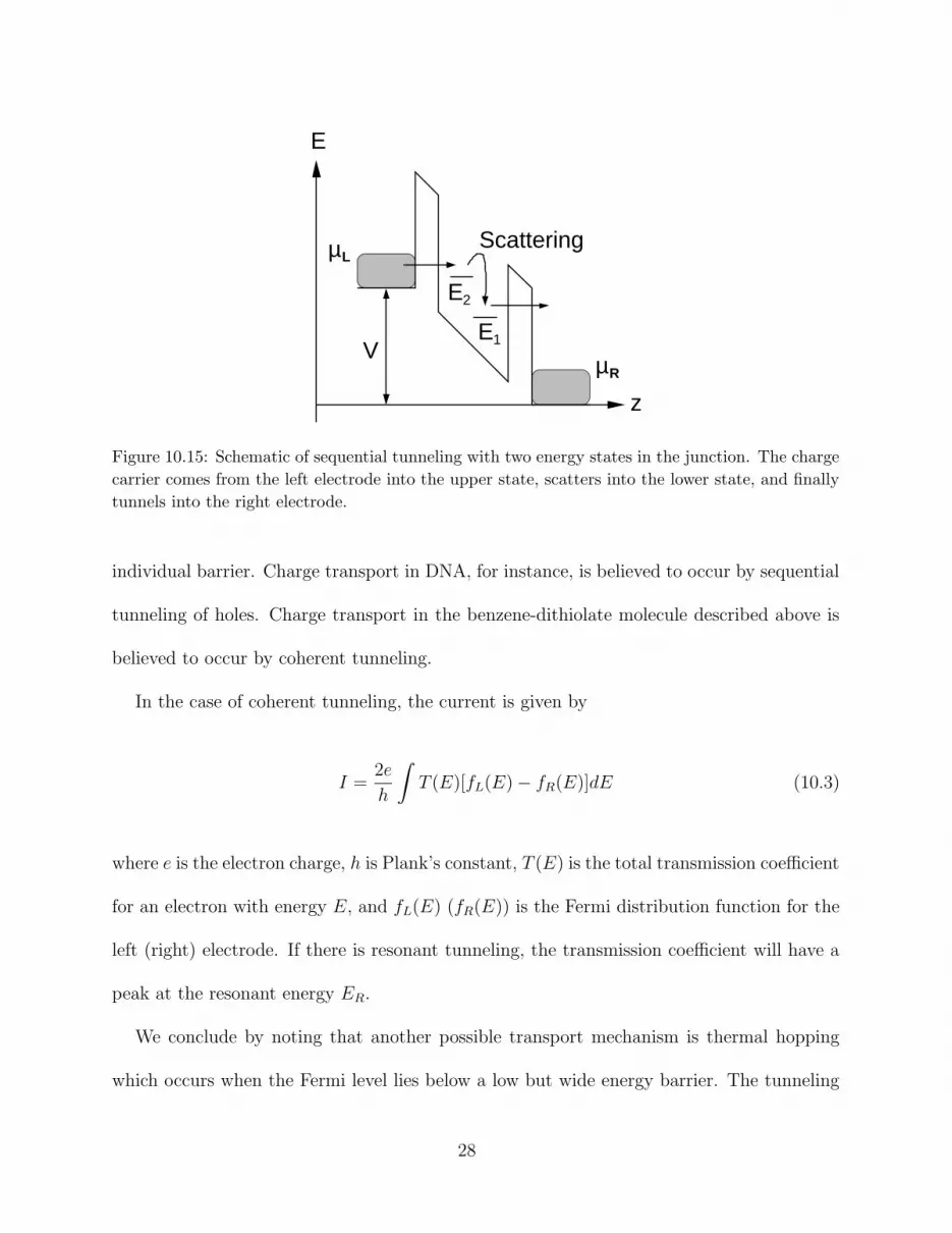
So far we have neglected any scattering effect that would change the energy of the electron
and/or its localization properties inside the quantum well. If such effects take place then
we can think of the electron as first resonant tunneling from, say, the left electrode into
the quantum well, then loosing part of its energy (or becoming localized) in the quantum
well, and finally tunneling into the right electrode. This phenomenon is called sequential
tunneling as opposed to coherent resonant tunneling described above. It is depicted in
Figure 10.15. Sequential tunneling can occur when the electron scatters off an impurity or
with a vibrational state in the junction. The scattering effect can be elastic or inelastic. In
the former case, the electron maintains its initial energy after scattering, in the latter, the
electron looses or gains energy. Both inelastic or elastic scattering effects can contribute to
sequential tunneling.
The rate (or probability) of coherent tunneling drops off dramatically with the distance
between the electrodes. However, sequential tunneling has smaller distance dependence since
the rate to transverse a series of barriers is just a product of the rates to transverse each
27
E1
µL
µR
E2
Scattering
E
z
V
Figure 10.15: Schematic of sequential tunneling with two energy states in the junction. The charge
carrier comes from the left electrode into the upper state, scatters into the lower state, and finally
tunnels into the right electrode.
individual barrier. Charge transport in DNA, for instance, is believed to occur by sequential
tunneling of holes. Charge transport in the benzene-dithiolate molecule described above is
believed to occur by coherent tunneling.
In the case of coherent tunneling, the current is given by
I =2e
h
∫
T (E)[fL(E)− fR(E)]dE (10.3)
where e is the electron charge, h is Plank’s constant, T (E) is the total transmission coefficient
for an electron with energy E, and fL(E) (fR(E)) is the Fermi distribution function for the
left (right) electrode. If there is resonant tunneling, the transmission coefficient will have a
peak at the resonant energy ER.
We conclude by noting that another possible transport mechanism is thermal hopping
which occurs when the Fermi level lies below a low but wide energy barrier. The tunneling
28
probability across the barrier is considerably suppressed due to the width of the barrier.
However, at higher temperatures, the electron can raise its energy with the assistance of a
vibrational mode (phonon mode of the structure). The electron is said to “hop” from one
side of the barrier to the other via an intermediate (phonon-assisted) state. While thermal
hopping has been invoked as a possible transport mechanism in DNA, it is unlikely it plays
a major role in the molecular devices described in the previous sections.
B. Current-induced mechanical effects
When current flows in a device it can affect its atomic structure by literally moving
the atoms (electromigration), as discussed in Section I, or by exciting vibrational modes and
heating up the system. Both effects have tremendous consequences in electronics and are still
not fully understood at the nanoscale. While in Section I we reported that electromigration
can be used to build molecular junctions, here we refer to the consequences of this effect on
the fully-formed device.
Electromigration is observed when a large current density flows into the device. In this
case, some of the momentum of the charge carriers is transferred to the ions, which are
consequently moved. In traditional microelectronics devices, this effect increases when the
dimensions of the device become small. It is natural to ask, then, if such an effect is detri-
mental for molecular devices. While more work is needed to understand this issue, it has
been experimentally demonstrated that carbon nanotubes can sustain current densities much
larger than normal microelectronic devices without current-induced break-up.29 Similarly,
theoretical work has shown that the benzene-dithiolate molecule described above should be
quite resistant to electromigration effects.30 Both results can be attributed to the strong
29
carbon-carbon bond.
Even less work has been done on the heating effects of molecular devices. Theoretical
results31 indicate that even though nanoscale junctions can heat up quite substantially when
current flows, the majority of such heat is dissipated into the bulk electrodes if the contacts
easily allow for heat conduction. Clearly, in a real structure both effects are present at the
same time. However, the interrelation between current-induced forces and heating is still
unclear.
IV. INTEGRATION STRATEGIES
Up to this point, we have discussed the fabrication and operation of molecular devices.
However, we need to recognize that most likely the major challenge of creating an electronics
from single molecules is not the fabrication of individual devices (though difficult), but to
integrate them into complex circuits. In traditional microelectronics, individual devices are
etched onto a larger microprocessor and connected by wires. A similar concept is envisioned
for molecular electronics where billions of single molecule devices should be connected in a
reliable (and desirably not too expensive) way. We conclude this chapter by discussing some
ideas and efforts toward this goal.
A. Defect tolerance and new molecular architectures
As the size of traditional microelectronics devices decreases, the fabrication costs increase
dramatically mainly because every component (or at least a large percentage) has to work
properly. In other words, the number of defects in the circuit has to be very small for the
30
circuit to function. If self-assembly will be the method of choice to build molecular devices,
then a large number of defects will likely be part of the circuit. With self-assembly, the
molecules are not as neatly aligned on a metal surface as one would like, and many of them
might not interact with the electrodes at all; thus creating domains with totally different
I-V characteristics. Since it is conceivable that such defects will be unavoidable, then defect-
tolerant architectures will be necessary so that the circuit keeps functioning even with a large
number of defects. Incidentally, this could lower the fabrication costs as less control on the
quality of each component is necessary.37 Clearly, there has to be some amount of defect
tolerance built into both the computer hardware and software (in the latter case, the term
“fault tolerance” is used). Here we just focus on the hardware.
Redundancy is one way to create a defect-tolerant architecture: By making many of the
same devices, i.e., devices with same functionalities, even if some of them do not work,
the circuit can still operate because it has access to the ones that still work. A practical
example of how to create such redundancy is provided by an experimental computer based
on a crossbar architecture. The latter is simply a series of horizontal lines (wires) crossing
a series of parallel lines (see the schematic in Figure 10.16). The points where the wires
intersect are the locations of the circuit elements. This computer, called Teramac and built
at Hewlett-Packard, used traditional microelectronic components. However, the computer
contained many (with respect to regular computer architectures) fatal hardware defects.
Many of the same components were hooked up in a crossbar architecture. This allowed for
software rerouting around the defective components, and thus, the computer was able to
work with very high percentage of defects.
A crossbar architecture was used, as well, to make a molecular memory. Previously, we
31
Figure 10.16: Schematic of a molecular memory built with a crossbar architecture. (From Ref. 18
by permission of the American Chemical Society.)
discussed molecular switches made of catenanes. These switches can be made by depositing
the molecules on parallel wires, and then depositing perpendicular wires on top (see Fig-
ure 10.16).18 Here, each molecular switch (which is comprised of a number of molecules) is
accessed by a bias across the two wires which cross at that point. The array of switches can
then act as a memory device, with each bit stored at the points where the wires cross. This
type of architecture seems thus promising for future computing applications.
V. CONCLUSIONS
We have given just a limited overview of the fundamental concepts and current research in
molecular electronics. We refer the reader to the reviews suggested below and original papers
to get a more detailed account. The field is expanding at a fast rate and many of the problems
we encounter today in making and integrating molecular devices might be overcome in the
future. However, irrespective of whether this electronics will become a commercial reality
or not, it is important to mention that we have learned, and will learn, a big deal regarding
the fundamental transport properties of nanoscale systems, and knowledge is always at the
heart of any technological revolution.
32
VI. QUESTIONS
Question 1 Show that at zero temperature, expression 10.3 can be written as
I =2e
h
∫ Ef,L
Ef,R
T (E)dE (10.4)
where Ef,L (Ef,R) is the Fermi energy of the left (right) electrode.
Question 2 Show that if the transmission coefficient, T (E), is energy independent and
equal to one, the conductance of a junction assumes the value 2e2/h, called the quantum of
conductance.
Question 3 For resonant tunneling, the total transmission coefficient will have a sharp
peak at the resonant energy ER. Consider the system shown in Figure 10.13, where there
is one discrete level in the junction above the Fermi level E0f at zero bias. Suppose the
transmission function T (E) is proportional to a sharply peaked Gaussian function plus a
constant. Take the standard deviation to be 10−2 eV, the Gaussian to be centered around
the energy ER = 10−1 eV (with E0
f = 0 eV for both electrodes at zero bias), and the constant
to be 1. Let the proportionality factor be 10−4 to keep the magnitudes within a reasonable
range. Assume the bands in the electrodes are large and that there is a linear drop in the
voltage across the junction. Plot T (E) on the interval [-1,1] eV. Now calculate and plot
the I-V curve using Equation 10.3 at zero temperature from a bias of 0 V to a bias of 1 V.
Assume 2e/h = 1.
Question 4 Now plot the differential resistance from the I-V curve of Question 3. Why
does the differential resistance have a broader peak than the transmission coefficient, when
the Fermi function is just a step function? Also, note that there is no region of negative
33
differential resistance.
Question 5 Increase the temperature and plot the I-V curve. What happens when you
increase the temperature to room temperature? If you increase the temperature further?
Why does this happen? Now plot the differential resistance, and note the difference between
the differential resistance in this case and the result of Question 4.
VII. FURTHER READING
• For more advanced readers, see Ref. 11 and Ref. 32 for a more complete discussion
of charge transport on the mesoscopic and molecular scale. Included in these two
references are details on how the transmission coefficient is calculated.
• For reviews of molecular electronics, see Ref. 13 and Refs. 33–36.
• For a review of catenanes and rotaxanes as molecular switches, see Ref. 18. Transport
in DNA and its application to nanoscale electronics are reviewed in Ref. 25.
34
1 A. Aviram and M. A. Ratner, Chem. Phys. Lett. 29, 277 (1974).
2 M. A. Reed, C. Zhou, C. J. Muller, T. P. Burgin, and J. M. Tour, Science 278, 252 (1997).
3 H. Park, J. Park, A. K. L. Lim, E. H. Anderson, A. P. Alivisatos, and P. L. McEuen, Nature
407, 57 (2000).
4 C. J. Muller, J. M. van Ruitenbeek, and L. J. de Jongh, Physica C 191, 485 (1992).
5 H. Park, A. K. L. Lim, A. P. Alivisatos, J. Park, and P. L. McEuen, Appl. Phys. Lett. 75, 301
(1999).
6 R. P. Andres, T. Bein, M. Dorogi, S. Feng, J. I. Henderson, C. P. Kubiak, W. Mahoney, R. G.
Osifchin, and R. Reifenberger, Science 272, 1323 (1996).
7 M. A. Reed, Proceedings of the IEEE 87, 652 (1999).
8 L. A. Bumm, J. J. Arnold, M. T. Cygan, T. D. Dunbar, T. P. Burgin, L. Jones, D. L. Allara, J.
M. Tour, and P. S. Weiss, Science 271, 1705 (1996).
9 E. G. Emberly and G. Kirczenow, Phys. Rev. B 58, 10911 (1998).
10 M. Di Ventra, S. T. Pantelides, N. D. Lang, Phys. Rev. Lett. 84, 979 (2000).
11 S. Datta, Electronic Transport in Mesoscopic Systems (Cambridge University Press, 1995).
12 See, e.g., C. J. Muller, J. M. Krans, T. N. Todorov, and M. A. Reed, Phys. Rev. B 53, 1022
(1996).
13 M. A. Ratner, Introducing molecular electronics, Materials Today, Feb, 20-27 (2002).
14 E. G. Emberly and G. Kirczenow, Phys. Rev. B 64, 235412 (2001).
15 Z. Q. Yang, N. D. Lang, and M. Di Ventra, Appl. Phys. Lett. 82, 1938 (2003).
16 N. D. Lang and Ph. Avouris, Nano. Lett. 2, 1047 (2002).
35
17 V. Derycke, R. Martel, J. Appenzeller, and Ph. Avouris, Appl. Phys. Lett. 80, 2773 (2002).
18 A. R. Pease, J. O. Jeppesen, J. Fraser Stoddart, Y. Luo, C. P. Collier, and J. R. Heath, Acc.
Chem. Res. 34, 433 (2001).
19 S. J. Tans, A. R. M. Verschueren, C. Dekker, Nature 393, 49 (1998).
20 M. Di Ventra, S. T. Pantelides, and N. D. Lang, Appl. Phys. Lett. 76, 3448 (2000).
21 J. Park, A. N. Pasupathy, J. I. Goldsmith, C. Chang, Y. Yaish, J. R. Petta, M. Rinkoski, J. P.
Sethna, H. D. Abruna, P. L. McEuen, and D. C. Ralph, Nature 417, 722 (2002).
22 W. Liang, M. P. Shores, M. Bockrath, J. R. Long, and H. Park, Nature 417, 725 (2002).
23 R. M. Metzger, B. Chen, U. Hopfner, M. V. Lakshmikantham, D. Vuillaume, T. Kawai, X. L.
Wu, H. Tachibana, T. V. Hughes, H. Sakurai, J. W. Baldwin, C. Hosch, M. P. Cava, L. Brehmer,
and G. J. Ashwell, J. Am. Chem. Soc. 119, 10455 (1997).
24 C. Dekker and M. A. Ratner, Electronic properties of DNA, Phys. World 14, 29 (2001).
25 M. Di Ventra and M. Zwolak, DNA Electronics in ”Encyclopedia of Nanoscience and Nanotech-
nology,” H. S. Nalwa (American Scientific Publishers, 2003).
26 J. Richter, Physica E 16, 157-173 (2003).
27 K. Keren, M. Krueger, R. Gilad, G. Ben-Yoseph, U. Sivan, and E. Braun, Science 297, 72
(2002).
28 P. Phillips, Advanced Solid State Physics (Westview Press, 2002).
29 P. J. de Pablo, E. Graugnard, B. Walsh, R. P. Andres, S. Datta, and R. Reifenberger, Appl.
Phys. Lett. 74 323 (1999).
30 M. Di Ventra, S. T. Pantelides, and N. D. Lang, Phys. Rev. Lett. 88, 046801 (2002).
31 M. J. Montgomery, T. N. Todorov, and A. P. Sutton, J. Phys. Cond. Mat. 14, 1 (2002).
36
32 V. Mujica and M. Ratner, Molecular Conductance Junctions: A Theory and Modeling Progress
Report in ”Handbook of Nanoscience, Engineering, and Technology,” W. A. Goddard III, D. W.
Brenner, S. E. Lyshevski, and G. J. Iafrate (CRC Press, 2002).
33 K. S. Kwok and J. C. Ellenbogen, Moletronics: future electronics, Materials Today, Feb, 28
(2002).
34 R. Lloyd Carroll and Christopher B. Gorman, The Genesis of Molecular Electronics, Acta Cryst.
B 41, 4379 (2002).
35 M. A. Reed and J. M. Tour, Computing with molecules, Scientific American, June, 86 (2000).
36 C. Joachim, J. K. Gimzewski, and A. Aviram, Electronics using hybrid-molecular and mono-
molecular devices, Nature 408, 541 (2000).
37 J. R. Heath, P. J. Kuekes, G. S. Snider, and R. S. Williams, Science 280, 1716 (1998).