Basic Electronics Prof. Dr. Chitralekha Mahanta Department of Electronics and Communication Engineering Indian Institute of Technology, Guwahati Module: 2 Bipolar Junction Transistors Lecture-6 BJT Amplifier – Part 1 In the last class we discussed about the different biasing schemes used for amplifiers and we studied about the significance of proper biasing scheme so that a week signal given as input can be faithfully amplified without any distortion occurring at any portion of the signal. Today we will discuss about the amplifier which is used for such amplification of week signal with different biasing schemes and today we will start discussing a BJT amplifier in the common emitter configuration. The common emitter BJT amplifier with fixed biasing scheme will be discussed first. The fixed biasing scheme as you have studied earlier is having a biasing resistance given here by this R b . This resistance is connected to base terminal and its shares the same V CC with the collector which is used for reverse biasing. We are taking for example an NPN transistor which is common emitter configuration. Here apart from these biasing resistances there are capacitances, which are used for coupling the signals. (Refer Slide Time: 2:36) The C 1 is the input coupling capacitor which is coupling the signal V S and the output which is obtained at the output terminals this output is V O and this output is obtained by coupling the collector with a capacitor C 2 and this V S which is the input signal this is having a series (00:03:00) resistance R S and we are getting the output voltage V O across this load resistance R L . This amplifier has the source resistance R S in series with the 1
Transcript
Basic Electronics Prof. Dr. Chitralekha Mahanta
Department of Electronics and Communication Engineering Indian Institute of Technology, Guwahati
Module: 2 Bipolar Junction Transistors
Lecture-6 BJT Amplifier – Part 1
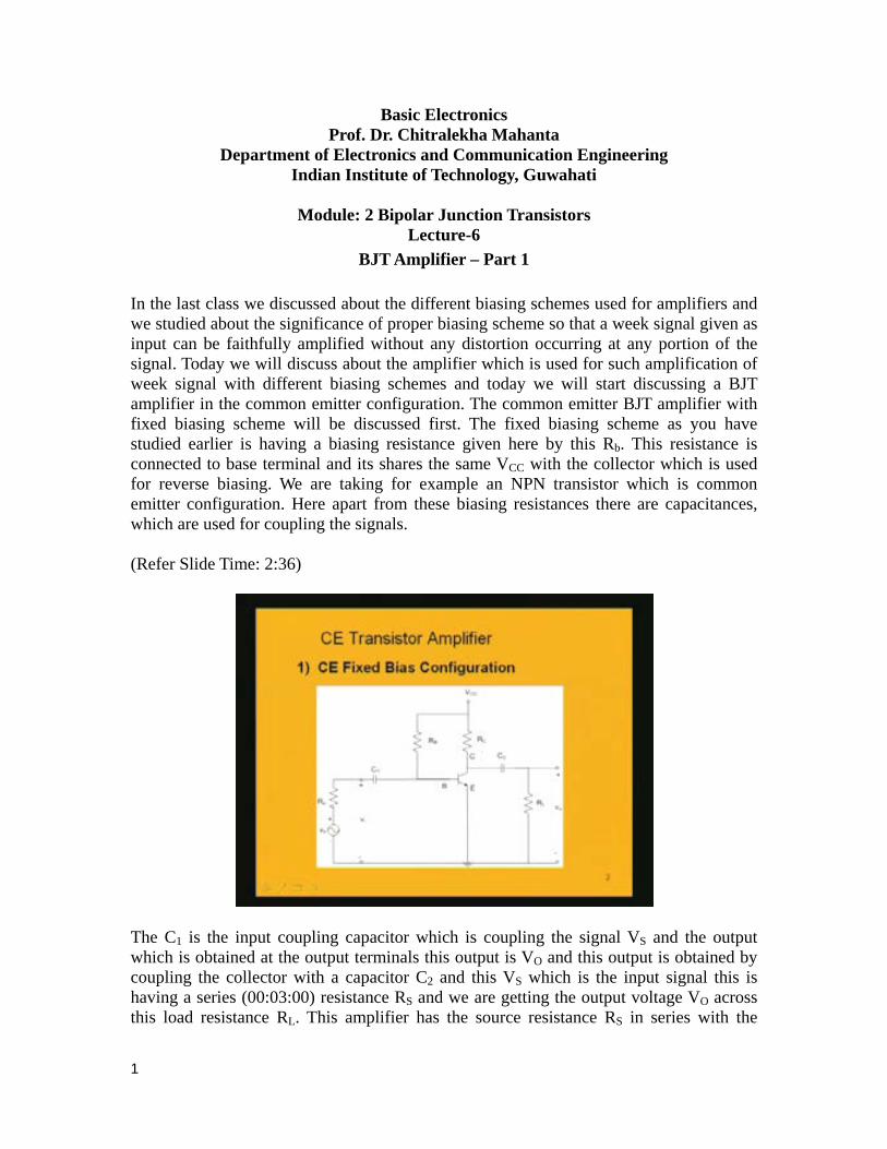
In the last class we discussed about the different biasing schemes used for amplifiers and we studied about the significance of proper biasing scheme so that a week signal given as input can be faithfully amplified without any distortion occurring at any portion of the signal. Today we will discuss about the amplifier which is used for such amplification of week signal with different biasing schemes and today we will start discussing a BJT amplifier in the common emitter configuration. The common emitter BJT amplifier with fixed biasing scheme will be discussed first. The fixed biasing scheme as you have studied earlier is having a biasing resistance given here by this Rb. This resistance is connected to base terminal and its shares the same VCC with the collector which is used for reverse biasing. We are taking for example an NPN transistor which is common emitter configuration. Here apart from these biasing resistances there are capacitances, which are used for coupling the signals. (Refer Slide Time: 2:36)
The C1 is the input coupling capacitor which is coupling the signal VS and the output which is obtained at the output terminals this output is VO and this output is obtained by coupling the collector with a capacitor C2 and this VS which is the input signal this is having a series (00:03:00) resistance RS and we are getting the output voltage VO across this load resistance RL. This amplifier has the source resistance RS in series with the
1
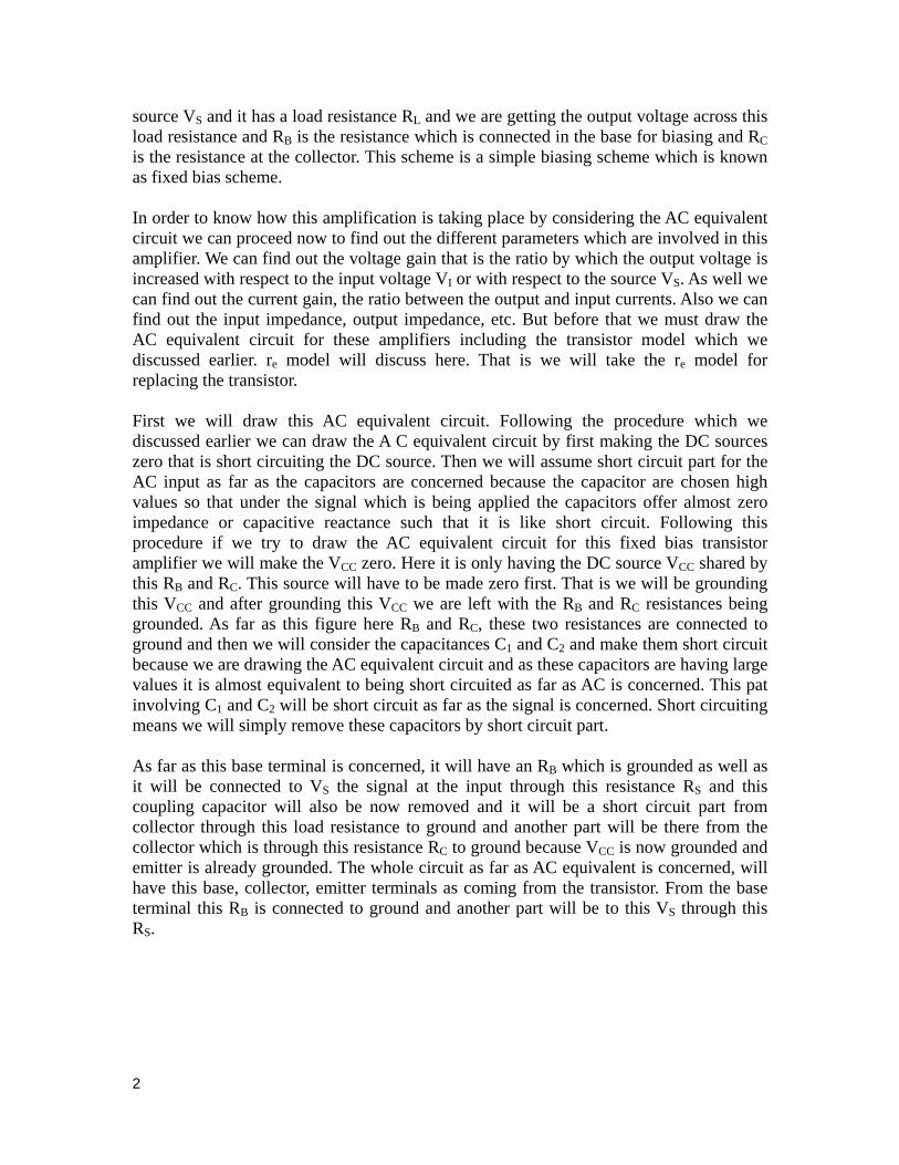
source VS and it has a load resistance RL and we are getting the output voltage across this load resistance and RB is the resistance which is connected in the base for biasing and RC is the resistance at the collector. This scheme is a simple biasing scheme which is known as fixed bias scheme. In order to know how this amplification is taking place by considering the AC equivalent circuit we can proceed now to find out the different parameters which are involved in this amplifier. We can find out the voltage gain that is the ratio by which the output voltage is increased with respect to the input voltage VI or with respect to the source VS. As well we can find out the current gain, the ratio between the output and input currents. Also we can find out the input impedance, output impedance, etc. But before that we must draw the AC equivalent circuit for these amplifiers including the transistor model which we discussed earlier. re model will discuss here. That is we will take the re model for replacing the transistor. First we will draw this AC equivalent circuit. Following the procedure which we discussed earlier we can draw the A C equivalent circuit by first making the DC sources zero that is short circuiting the DC source. Then we will assume short circuit part for the AC input as far as the capacitors are concerned because the capacitor are chosen high values so that under the signal which is being applied the capacitors offer almost zero impedance or capacitive reactance such that it is like short circuit. Following this procedure if we try to draw the AC equivalent circuit for this fixed bias transistor amplifier we will make the VCC zero. Here it is only having the DC source VCC shared by this RB and RC. This source will have to be made zero first. That is we will be grounding this VCC and after grounding this VCC we are left with the RB and RC resistances being grounded. As far as this figure here RB and RC, these two resistances are connected to ground and then we will consider the capacitances C1 and C2 and make them short circuit because we are drawing the AC equivalent circuit and as these capacitors are having large values it is almost equivalent to being short circuited as far as AC is concerned. This pat involving C1 and C2 will be short circuit as far as the signal is concerned. Short circuiting means we will simply remove these capacitors by short circuit part. As far as this base terminal is concerned, it will have an RB which is grounded as well as it will be connected to VS the signal at the input through this resistance RS and this coupling capacitor will also be now removed and it will be a short circuit part from collector through this load resistance to ground and another part will be there from the collector which is through this resistance RC to ground because VCC is now grounded and emitter is already grounded. The whole circuit as far as AC equivalent is concerned, will have this base, collector, emitter terminals as coming from the transistor. From the base terminal this RB is connected to ground and another part will be to this VS through this RS.
2
(Refer Slide Time: 7:07)
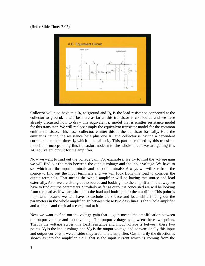
Collector will also have this RC to ground and RL is the load resistance connected at the collector to ground; it will be there as far as this transistor is considered and we have already discussed how to draw this equivalent re model that is emitter resistance model for this transistor. We will replace simply the equivalent transistor model for the common emitter transistor. This base, collector, emitter this is the transistor basically. Here the emitter is having the resistance beta plus one RE and collector is having a dependent current source beta times IB which is equal to IC. This part is replaced by this transistor model and incorporating this transistor model into the whole circuit we are getting this AC equivalent circuit for the amplifier. Now we want to find out the voltage gain. For example if we try to find the voltage gain we will find out the ratio between the output voltage and the input voltage. We have to see which are the input terminals and output terminals? Always we will see from the source to find out the input terminals and we will look from this load to consider the output terminals. That means the whole amplifier will be having the source and load externally. As if we are sitting at the source and looking into the amplifier, in that way we have to find out the parameters. Similarly as far as output is concerned we will be looking from the load as if we are sitting on the load and looking into the amplifier. This point is important because we will have to exclude the source and load while finding out the parameters in the whole amplifier. In between these two dash lines is the whole amplifier and a source and the load are external to it. Now we want to find out the voltage gain that is gain means the amplification between the output voltage and input voltage. The output voltage is between these two points. That is the voltage across this load resistance and input voltage is between these two points. VI is the input voltage and VO is the output voltage and conventionally this input and output currents if we consider they are into the amplifier. Customarily the direction is shown as into the amplifier. So II that is the input current which is coming from the
3
source, it will be flowing into the amplifier at this input terminal, so this is the input current and output current at this output terminal into the amplifier. The IO current is flowing through this resistance RL into the amplifier and input current is coming from source into the amplifier. If we look into this input current we notice that the input current is having two parts. One part is through this resistance RB and other part of the current is through this resistance beta plus one RE. This input current basically has two parts: one is through this, one is through this and if we consider the current source of the output, IC is the current source which is equal to beta times of IB and the current which will be flowing, will be flowing in this direction. It will be going to the output side; input current, base current will be coming and it will be flowing like this. Here the beta times of IB current which is the collector current has actually three parts: one is through this RC, one is through this RO. RO is the output resistance of the transistor. We generally ignore this because it is having a very high value in the order of mega ohm but to be exact this should be there and after words we can ignore. If we are told that it is very, very large you can ignore it. But for time being while drawing the exact equivalent circuit we will be having this RO at the output side. This RO is the output resistance of the common emitter transistor and that is generally having very high value. (Refer Slide Time: 11:07)
This collector current beta times of ib has three parts one is through RC and one is through this RO and other is through this RL which is nothing but the conventional output current io as it is shown here. We want to find input impedance; Zi is denoting the input impedance. We have to take the input terminals; the voltage at this input terminal is vi divided by the current ii. Input voltage by input current will be the input impedance and output impedance we will look into the output terminals from the load and we will find out what is the output impedance by taking the ratio between vo and io that is vo by io making the input source zero. That is vs you make zero that will make vi zero means ib
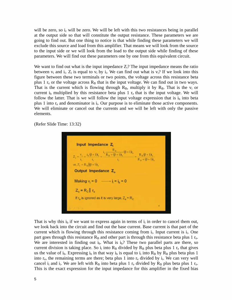
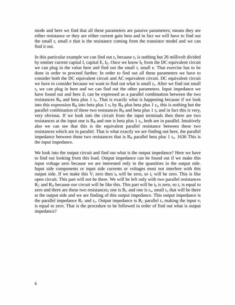
4
will be zero, so ic will be zero. We will be left with this two resistances being in parallel at the output side so that will constitute the output resistance. These parameters we are going to find out. But one thing to notice is that while finding these parameters we will exclude this source and load from this amplifier. That means we will look from the source to the input side or we will look from the load to the output side while finding of these parameters. We will find out these parameters one by one from this equivalent circuit. We want to find out what is the input impedance Zi? The input impedance means the ratio between vi and ii. Zi is equal to vi by ii. We can find out what is vi? If we look into this figure between these two terminals or two points, the voltage across this resistance beta plus 1 re or the voltage across RB that is the input voltage. We can find out in two ways. That is the current which is flowing through RB, multiply it by RB. That is the vi or current ib multiplied by this resistance beta plus 1 re that is the input voltage. We will follow the latter. That is we will follow the input voltage expression that is ib into beta plus 1 into re and denominator is ii. Our purpose is to eliminate those active components. We will eliminate or cancel out the currents and we will be left with only the passive elements. (Refer Slide Time: 13:32)
That is why this ib if we want to express again in terms of ii in order to cancel them out, we look back into the circuit and find out the base current. Base current is that part of the current which is flowing through this resistance coming from ii. Input current is ii. One part goes through this resistance RB and other part is through this resistance beta plus 1 re. We are interested in finding out ib. What is ib? These two parallel parts are there, so current division is taking place. So ii into RB divided by RB plus beta plus 1 re that gives us the value of ib. Expressing ib in that way ib is equal to ii into RB by RB plus beta plus 1 into re, the remaining terms are there; beta plus 1 into re divided by ii. We can very well cancel ii and ii. We are left with RB into beta plus 1 re divided by RB plus beta plus 1 re. This is the exact expression for the input impedance for this amplifier in the fixed bias
5
mode and here we find that all these parameters are passive parameters; means they are either resistance or they are either current gain beta and in fact we will have to find out the small r, small e that is the resistance coming from the transistor model and we can find it out. In this particular example we can find out re because re is nothing but 26 millivolt divided by emitter current capital I, capital E, IE. Once we know IE from the DC equivalent circuit we can plug in the value here and find out the small r, small e. That exercise has to be done in order to proceed further. In order to find out all these parameters we have to consider both the DC equivalent circuit and AC equivalent circuit. DC equivalent circuit we have to consider because we want to find out what is small re. After we find out small re we can plug in here and we can find out the other parameters. Input impedance we have found out and here Zi can be expressed as a parallel combination between the two resistances RB and beta plus 1 re. That is exactly what is happening because if we look into this expression RB into beta plus 1 re by RB plus beta plus 1 re, this is nothing but the parallel combination of these two resistances RB and beta plus 1 re and in fact this is very, very obvious. If we look into the circuit from the input terminals then there are two resistances at the input one is RB and one is beta plus 1 re, both are in parallel. Intuitively also we can see that this is the equivalent parallel resistance between these two resistances which are in parallel. That is what exactly we are finding out here, the parallel impedance between these two resistances that is RB parallel beta plus 1 re. 1636 This is the input impedance. We look into the output circuit and find out what is the output impedance? Here we have to find out looking from this load. Output impedance can be found out if we make this input voltage zero because we are interested only in the quantities in the output side. Input side components or input side currents or voltages must not interfere with this output side. If we make this Vi zero then ib will be zero, so ic will be zero. This is like open circuit. This part will not be there. We will be left only with two parallel resistances RC and RO because our circuit will be like this. This part will be ib is zero, so ic is equal to zero and there are these two resistances; one is RC and one is ro, small ro that will be there at the output side and we are finding of this output impedance. This output impedance is the parallel impedance RC and ro. Output impedance is RC parallel ro making the input vi is equal to zero. That is the procedure to be followed in order of find out what is output impedance?
6
(Refer Slide Time: 17:45)
At this point I want to mention that if ro is considered to be very, very large which is actually the case, it is in the order of meg ohm; 10 to the power 6. As compared to RC it is higher. So we can neglect this resistance or we can ignore this resistance because it is very high, it is almost like infinity. If it is very high or infinite what will happen is that there will be practically no current in this part. Because it is offering infinite impedance current will not flow in this part. That means it is like open circuit, ro will be simply ignored. Then we are left with only RC. Then we can say that RC is the output resistance. This is the case when you ignore ro. ro means the output resistance of the transistor. These two parameters Zi and Zo we have found out. What about the voltage again? (Refer Slide Time: 18:37)
7
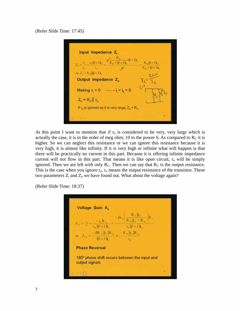
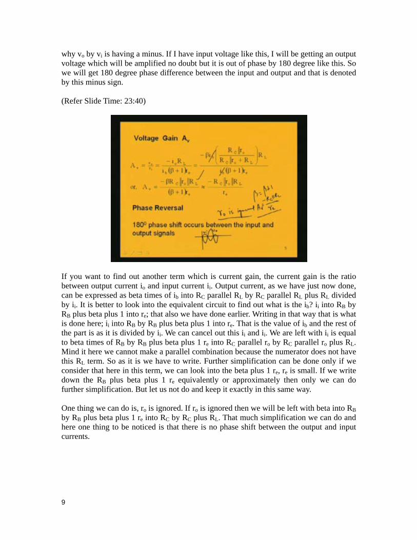
Voltage again is the ratio between the output voltage and input voltage. That means it is a ratio between vo and vi. If we look back what is vo here? This vo is nothing but io into RL but with a minus sign because we have denoted vo upper point is positive with respective to the ground but this io is following in this direction. This is io. io is this current. It is flowing from higher potential to lower potential as far as this sign is concerned. The voltage drop if we consider it as vo it will be io into RL with a minus sign. Minus ioRL will be equal to vo because as far as direction of current this is positive point, this is negative point. But voltage we have denoted as vo as upper point is positive. vo is equal to minus io into RL and input voltage we know. We have already found the input voltage is ib into beta plus 1 re. Replacing these values here vo is equal to minus io into RL and vi is equal to ib into beta plus 1 re. Again we replace the io. If we look back into the circuit, what is io? io is that part of current of ic which is flowing through this resistance of RL because if we look into this output side the current source is beta times ib which is equal to ic. This current is flowing in this output side and this current has three parts. As I have just now mentioned one part of current beta times ib is flowing through RC, other part is through ro and other part is through RL and we are interested in finding out that part io. If we combine these two RC and ro together as RC parallel ro that is one resistance; other is RL. According to current division beta times of ib is divided into this parallel resistance and this resistance. We are interested in finding out this current through this resistance RL. That will be equal to beta times ib into this equivalent parallel combination RC parallel RL divided by RC parallel ro plus RL. That is written here. Beta times of ib; minus sign is there because minus ioRL is the voltage at the output. Here we are replacing this io by beta times ib into RC parallel ro by RC parallel ro plus RL into RL. RL is already there in the original expression and vi input voltage is given by ib into beta plus 1 into re. We can further simplify this expression by writing minus beta into ib, ib cancel. Upper term or the numerator term if we again consider it is nothing but parallel combination between these three resistances RC, small ro and capital R capital L, RL. Because this is RC parallel ro into RL divided by RC parallel ro plus RL. This is the parallel combination between this and this. Finally we have a parallel combination between all the three in the numerator divided by beta plus 1 into re. Beta and beta plus 1 are almost equal because beta is a high value; suppose 100 and 101 there is not much difference it is almost equal. We can conveniently cancel them out. Then it gives a further simplified expression and that is equal to minus RC parallel ro parallel RL by re and here again if we now consider that ro is very high then we can further ignore ro and if ro is ignored then we will get another further simplified expression of Av which is equal to minus RC parallel RL divided by re, small re. This is a very, very simple expression to remember because now we have ignored ro because it is very high. But this is the exact expression and further simplification can be done conveniently looking into the practical aspects. One thing to be noted here is the minus sign. Actually this minus sign has significance or it has a meaning because minus sign means the phase reversal of 180 degree or the output voltage is out of phase by 180 degree with the input. That is actually denoted by this minus sign. 180 degree phase shift occurs between the input and output signals. That is
8
why vo by vi is having a minus. If I have input voltage like this, I will be getting an output voltage which will be amplified no doubt but it is out of phase by 180 degree like this. So we will get 180 degree phase difference between the input and output and that is denoted by this minus sign. (Refer Slide Time: 23:40)
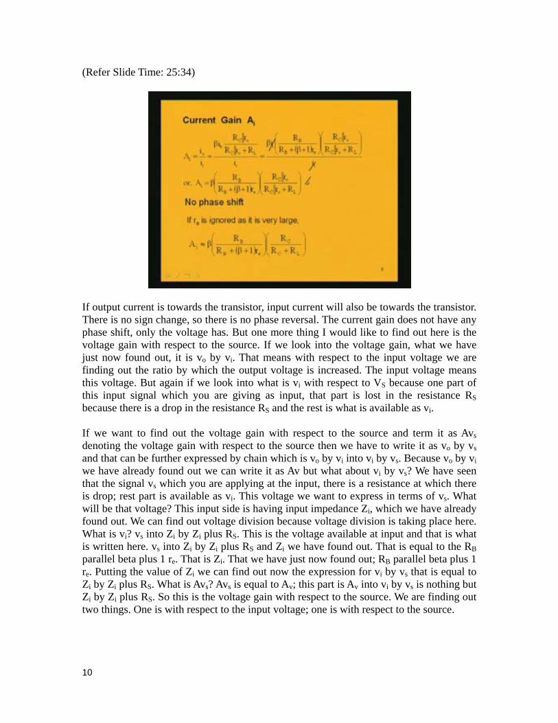
If you want to find out another term which is current gain, the current gain is the ratio between output current io and input current ii. Output current, as we have just now done, can be expressed as beta times of ib into RC parallel RL by RC parallel RL plus RL divided by ii. It is better to look into the equivalent circuit to find out what is the ib? ii into RB by RB plus beta plus 1 into re; that also we have done earlier. Writing in that way that is what is done here; ii into RB by RB plus beta plus 1 into re. That is the value of ib and the rest of the part is as it is divided by ii. We can cancel out this ii and ii. We are left with ii is equal to beta times of RB by RB plus beta plus 1 re into RC parallel ro by RC parallel ro plus RL. Mind it here we cannot make a parallel combination because the numerator does not have this RL term. So as it is we have to write. Further simplification can be done only if we consider that here in this term, we can look into the beta plus 1 re, re is small. If we write down the RB plus beta plus 1 re equivalently or approximately then only we can do further simplification. But let us not do and keep it exactly in this same way. One thing we can do is, ro is ignored. If ro is ignored then we will be left with beta into RB by RB plus beta plus 1 re into RC by RC plus RL. That much simplification we can do and here one thing to be noticed is that there is no phase shift between the output and input currents.
9
(Refer Slide Time: 25:34)
If output current is towards the transistor, input current will also be towards the transistor. There is no sign change, so there is no phase reversal. The current gain does not have any phase shift, only the voltage has. But one more thing I would like to find out here is the voltage gain with respect to the source. If we look into the voltage gain, what we have just now found out, it is vo by vi. That means with respect to the input voltage we are finding out the ratio by which the output voltage is increased. The input voltage means this voltage. But again if we look into what is vi with respect to VS because one part of this input signal which you are giving as input, that part is lost in the resistance RS because there is a drop in the resistance RS and the rest is what is available as vi. If we want to find out the voltage gain with respect to the source and term it as Avs denoting the voltage gain with respect to the source then we have to write it as vo by vs and that can be further expressed by chain which is vo by vi into vi by vs. Because vo by vi we have already found out we can write it as Av but what about vi by vs? We have seen that the signal vs which you are applying at the input, there is a resistance at which there is drop; rest part is available as vi. This voltage we want to express in terms of vs. What will be that voltage? This input side is having input impedance Zi, which we have already found out. We can find out voltage division because voltage division is taking place here. What is vi? vs into Zi by Zi plus RS. This is the voltage available at input and that is what is written here. vs into Zi by Zi plus RS and Zi we have found out. That is equal to the RB parallel beta plus 1 re. That is Zi. That we have just now found out; RB parallel beta plus 1 re. Putting the value of Zi we can find out now the expression for vi by vs that is equal to Zi by Zi plus RS. What is Avs? Avs is equal to Av; this part is Av into vi by vs is nothing but Zi by Zi plus RS. So this is the voltage gain with respect to the source. We are finding out two things. One is with respect to the input voltage; one is with respect to the source.
10
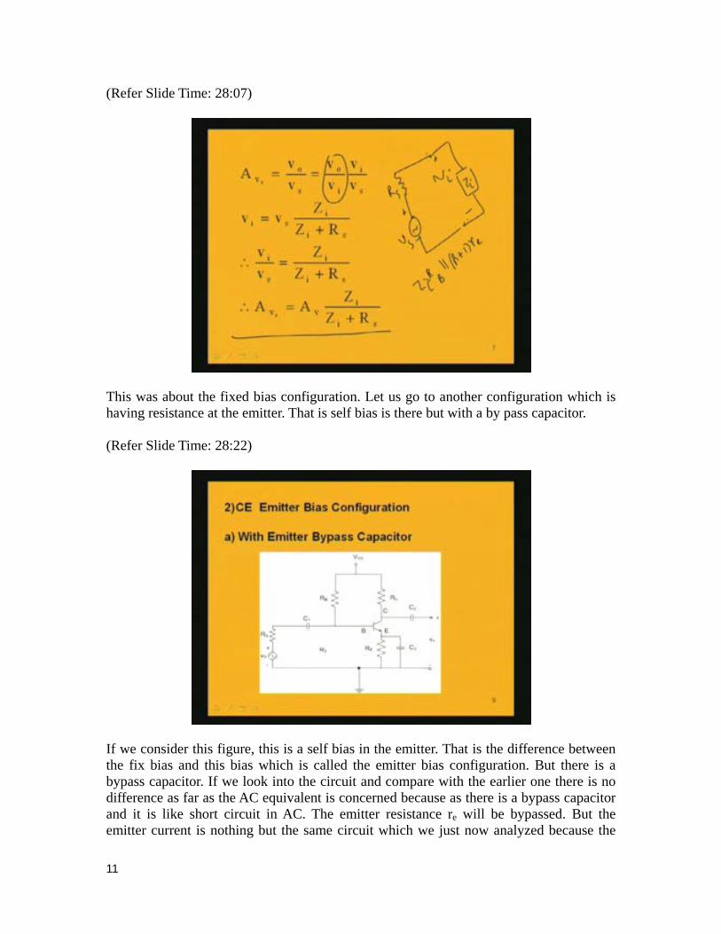
(Refer Slide Time: 28:07)
This was about the fixed bias configuration. Let us go to another configuration which is having resistance at the emitter. That is self bias is there but with a by pass capacitor. (Refer Slide Time: 28:22)
If we consider this figure, this is a self bias in the emitter. That is the difference between the fix bias and this bias which is called the emitter bias configuration. But there is a bypass capacitor. If we look into the circuit and compare with the earlier one there is no difference as far as the AC equivalent is concerned because as there is a bypass capacitor and it is like short circuit in AC. The emitter resistance re will be bypassed. But the emitter current is nothing but the same circuit which we just now analyzed because the
11
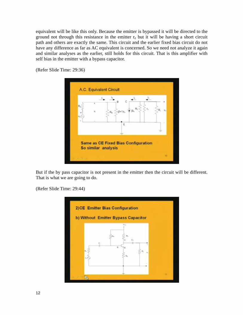
equivalent will be like this only. Because the emitter is bypassed it will be directed to the ground not through this resistance in the emitter re but it will be having a short circuit path and others are exactly the same. This circuit and the earlier fixed bias circuit do not have any difference as far as AC equivalent is concerned. So we need not analyze it again and similar analyses as the earlier, still holds for this circuit. That is this amplifier with self bias in the emitter with a bypass capacitor. (Refer Slide Time: 29:36)
But if the by pass capacitor is not present in the emitter then the circuit will be different. That is what we are going to do. (Refer Slide Time: 29:44)
12
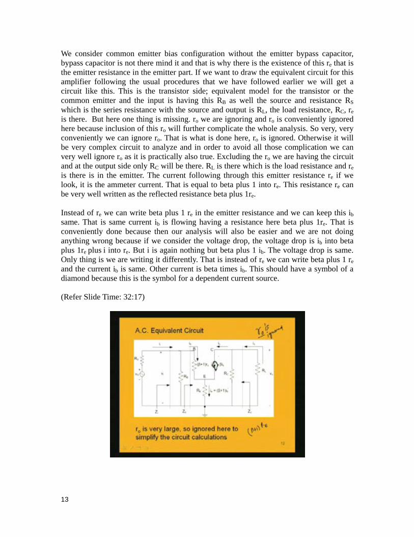
We consider common emitter bias configuration without the emitter bypass capacitor, bypass capacitor is not there mind it and that is why there is the existence of this re that is the emitter resistance in the emitter part. If we want to draw the equivalent circuit for this amplifier following the usual procedures that we have followed earlier we will get a circuit like this. This is the transistor side; equivalent model for the transistor or the common emitter and the input is having this RB as well the source and resistance RS which is the series resistance with the source and output is RL, the load resistance, RC, re is there. But here one thing is missing. ro we are ignoring and ro is conveniently ignored here because inclusion of this ro will further complicate the whole analysis. So very, very conveniently we can ignore ro. That is what is done here, ro is ignored. Otherwise it will be very complex circuit to analyze and in order to avoid all those complication we can very well ignore ro as it is practically also true. Excluding the ro we are having the circuit and at the output side only RC will be there. RL is there which is the load resistance and re is there is in the emitter. The current following through this emitter resistance re if we look, it is the ammeter current. That is equal to beta plus 1 into re. This resistance re can be very well written as the reflected resistance beta plus 1re. Instead of re we can write beta plus 1 re in the emitter resistance and we can keep this ib same. That is same current ib is flowing having a resistance here beta plus 1re. That is conveniently done because then our analysis will also be easier and we are not doing anything wrong because if we consider the voltage drop, the voltage drop is ib into beta plus 1re plus i into re. But i is again nothing but beta plus 1 ib. The voltage drop is same. Only thing is we are writing it differently. That is instead of re we can write beta plus 1 re and the current ib is same. Other current is beta times ib. This should have a symbol of a diamond because this is the symbol for a dependent current source. (Refer Slide Time: 32:17)
13
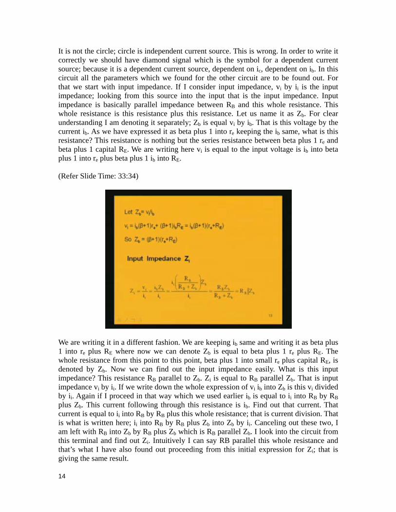
It is not the circle; circle is independent current source. This is wrong. In order to write it correctly we should have diamond signal which is the symbol for a dependent current source; because it is a dependent current source, dependent on ic, dependent on ib. In this circuit all the parameters which we found for the other circuit are to be found out. For that we start with input impedance. If I consider input impedance, vi by ii is the input impedance; looking from this source into the input that is the input impedance. Input impedance is basically parallel impedance between RB and this whole resistance. This whole resistance is this resistance plus this resistance. Let us name it as Zb. For clear understanding I am denoting it separately; Zb is equal vi by ib. That is this voltage by the current ib. As we have expressed it as beta plus 1 into re keeping the ib same, what is this resistance? This resistance is nothing but the series resistance between beta plus 1 re and beta plus 1 capital RE. We are writing here vi is equal to the input voltage is ib into beta plus 1 into re plus beta plus 1 ib into RE. (Refer Slide Time: 33:34)
We are writing it in a different fashion. We are keeping ib same and writing it as beta plus 1 into re plus RE where now we can denote Zb is equal to beta plus 1 re plus RE. The whole resistance from this point to this point, beta plus 1 into small re plus capital RE, is denoted by Zb. Now we can find out the input impedance easily. What is this input impedance? This resistance RB parallel to Zb. Zi is equal to RB parallel Zb. That is input impedance vi by ii. If we write down the whole expression of vi ib into Zb is this vi divided by ii. Again if I proceed in that way which we used earlier ib is equal to ii into RB by RB plus Zb. This current following through this resistance is ib. Find out that current. That current is equal to ii into RB by RB plus this whole resistance; that is current division. That is what is written here; ii into RB by RB plus Zb into Zb by ii. Canceling out these two, I am left with RB into Zb by RB plus Zb which is RB parallel Zb. I look into the circuit from this terminal and find out Zi. Intuitively I can say RB parallel this whole resistance and that’s what I have also found out proceeding from this initial expression for Zi; that is giving the same result.
14
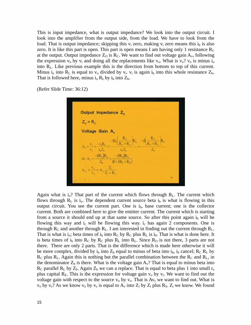
This is input impedance, what is output impedance? We look into the output circuit. I look into the amplifier from the output side, from the load. We have to look from the load. That is output impedance; skipping this vi zero, making vi zero means this ib is also zero. It is like this part is open. This part is open means I am having only 1 resistance RC at the output. Output impedance ZO is RC. We want to find out voltage gain Av, following the expression vo by vi and doing all the replacements like vo. What is vo? vo is minus io into RL. Like previous example this is the direction from bottom to top of this current. Minus io into RL is equal to vo divided by vi. vi is again ib into this whole resistance Zb. That is followed here, minus io RL by ib into Zb. (Refer Slide Time: 36:12)
Again what is io? That part of the current which flows through RL. The current which flows through RL is io. The dependent current source beta ib is what is flowing in this output circuit. You see the current part. One is ib, base current; one is the collector current. Both are combined here to give the emitter current. The current which is starting from a source it should end up at that same source. So after this point again ib will be flowing this way and ic will be flowing this way. ic has again 2 components. One is through RC and another through RL. I am interested in finding out the current through RL. That is what is io; beta times of ib into RC by RC plus RL is i0. That is what is done here. It is beta times of ib into RC by RC plus RL into RL. Since RO is not there, 3 parts are not there. There are only 2 parts. That is the difference which is made here otherwise it will be more complex, divided by ib into Zb equal to minus of beta into ib, ib cancel; RC RL by RC plus RL. Again this is nothing but the parallel combination between the RC and RL, in the denominator Zb is there. What is the voltage gain Av? That is equal to minus beta into RC parallel RL by Zb. Again Zb we can a replace. That is equal to beta plus 1 into small re plus capital RE. This is the expression for voltage gain vo by vi. We want to find out the voltage gain with respect to the source vo by vs. That is Avs we want to find out. What is vo by vs? As we know vo by vs is equal to Av into Zi by Zi plus RS. Zi we know. We found
15
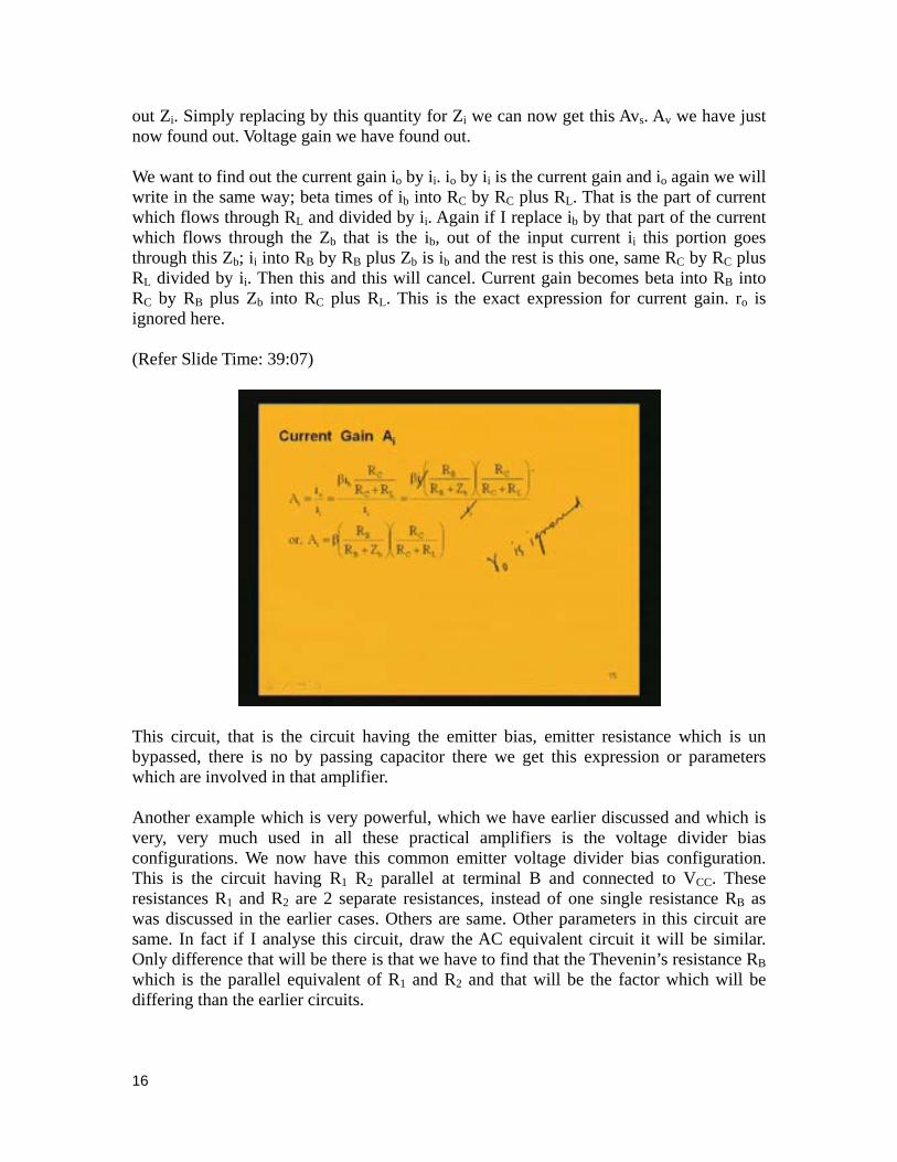
out Zi. Simply replacing by this quantity for Zi we can now get this Avs. Av we have just now found out. Voltage gain we have found out. We want to find out the current gain io by ii. io by ii is the current gain and io again we will write in the same way; beta times of ib into RC by RC plus RL. That is the part of current which flows through RL and divided by ii. Again if I replace ib by that part of the current which flows through the Zb that is the ib, out of the input current ii this portion goes through this Zb; ii into RB by RB plus Zb is ib and the rest is this one, same RC by RC plus RL divided by ii. Then this and this will cancel. Current gain becomes beta into RB into RC by RB plus Zb into RC plus RL. This is the exact expression for current gain. ro is ignored here. (Refer Slide Time: 39:07)
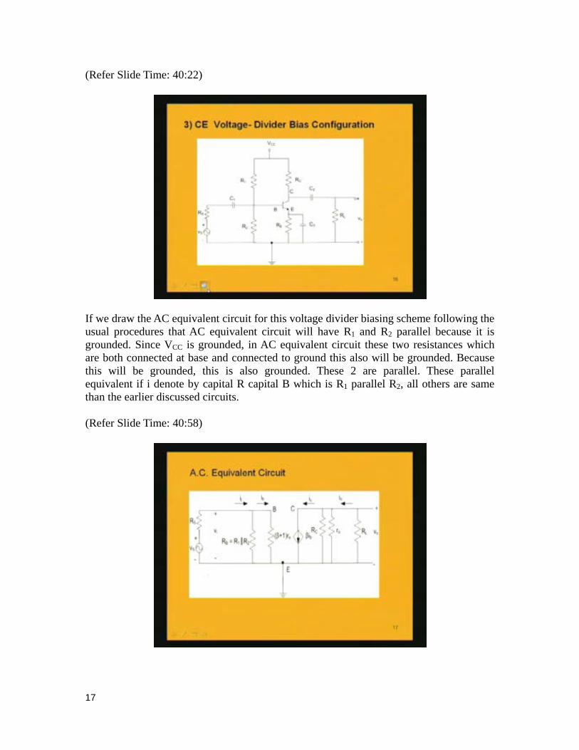
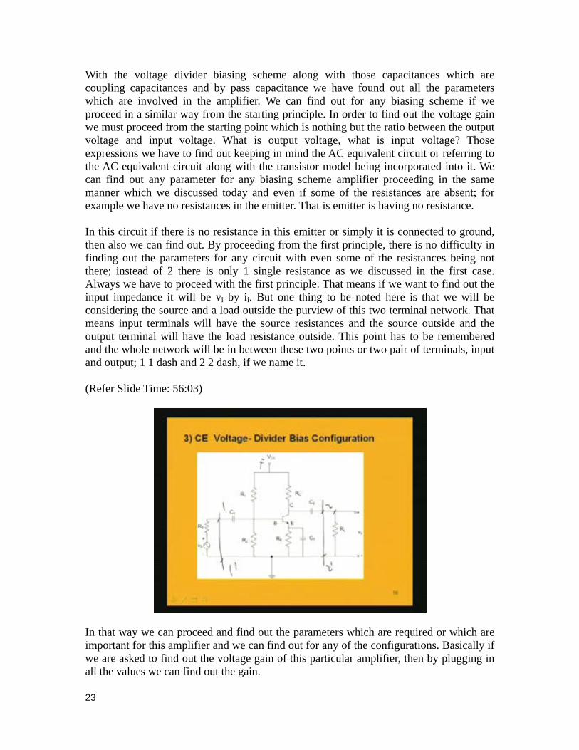
This circuit, that is the circuit having the emitter bias, emitter resistance which is un bypassed, there is no by passing capacitor there we get this expression or parameters which are involved in that amplifier. Another example which is very powerful, which we have earlier discussed and which is very, very much used in all these practical amplifiers is the voltage divider bias configurations. We now have this common emitter voltage divider bias configuration. This is the circuit having R1 R2 parallel at terminal B and connected to VCC. These resistances R1 and R2 are 2 separate resistances, instead of one single resistance RB as was discussed in the earlier cases. Others are same. Other parameters in this circuit are same. In fact if I analyse this circuit, draw the AC equivalent circuit it will be similar. Only difference that will be there is that we have to find that the Thevenin’s resistance RB which is the parallel equivalent of R1 and R2 and that will be the factor which will be differing than the earlier circuits.
16
(Refer Slide Time: 40:22)
If we draw the AC equivalent circuit for this voltage divider biasing scheme following the usual procedures that AC equivalent circuit will have R1 and R2 parallel because it is grounded. Since VCC is grounded, in AC equivalent circuit these two resistances which are both connected at base and connected to ground this also will be grounded. Because this will be grounded, this is also grounded. These 2 are parallel. These parallel equivalent if i denote by capital R capital B which is R1 parallel R2, all others are same than the earlier discussed circuits. (Refer Slide Time: 40:58)
17
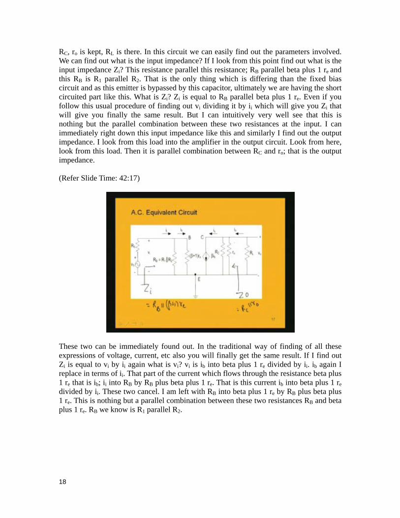
RC, ro is kept, RL is there. In this circuit we can easily find out the parameters involved. We can find out what is the input impedance? If I look from this point find out what is the input impedance Zi? This resistance parallel this resistance; RB parallel beta plus 1 re and this RB is R1 parallel R2. That is the only thing which is differing than the fixed bias circuit and as this emitter is bypassed by this capacitor, ultimately we are having the short circuited part like this. What is Zi? Zi is equal to RB parallel beta plus 1 re. Even if you follow this usual procedure of finding out vi dividing it by ii which will give you Zi that will give you finally the same result. But I can intuitively very well see that this is nothing but the parallel combination between these two resistances at the input. I can immediately right down this input impedance like this and similarly I find out the output impedance. I look from this load into the amplifier in the output circuit. Look from here, look from this load. Then it is parallel combination between RC and ro; that is the output impedance. (Refer Slide Time: 42:17)
These two can be immediately found out. In the traditional way of finding of all these expressions of voltage, current, etc also you will finally get the same result. If I find out Zi is equal to vi by ii again what is vi? vi is ib into beta plus 1 re divided by ii. ib again I replace in terms of ii. That part of the current which flows through the resistance beta plus 1 re that is ib; ii into RB by RB plus beta plus 1 re. That is this current ib into beta plus 1 re divided by ii. These two cancel. I am left with RB into beta plus 1 re by RB plus beta plus 1 re. This is nothing but a parallel combination between these two resistances RB and beta plus 1 re. RB we know is R1 parallel R2.
18
(Refer Slide Time: 43:13)
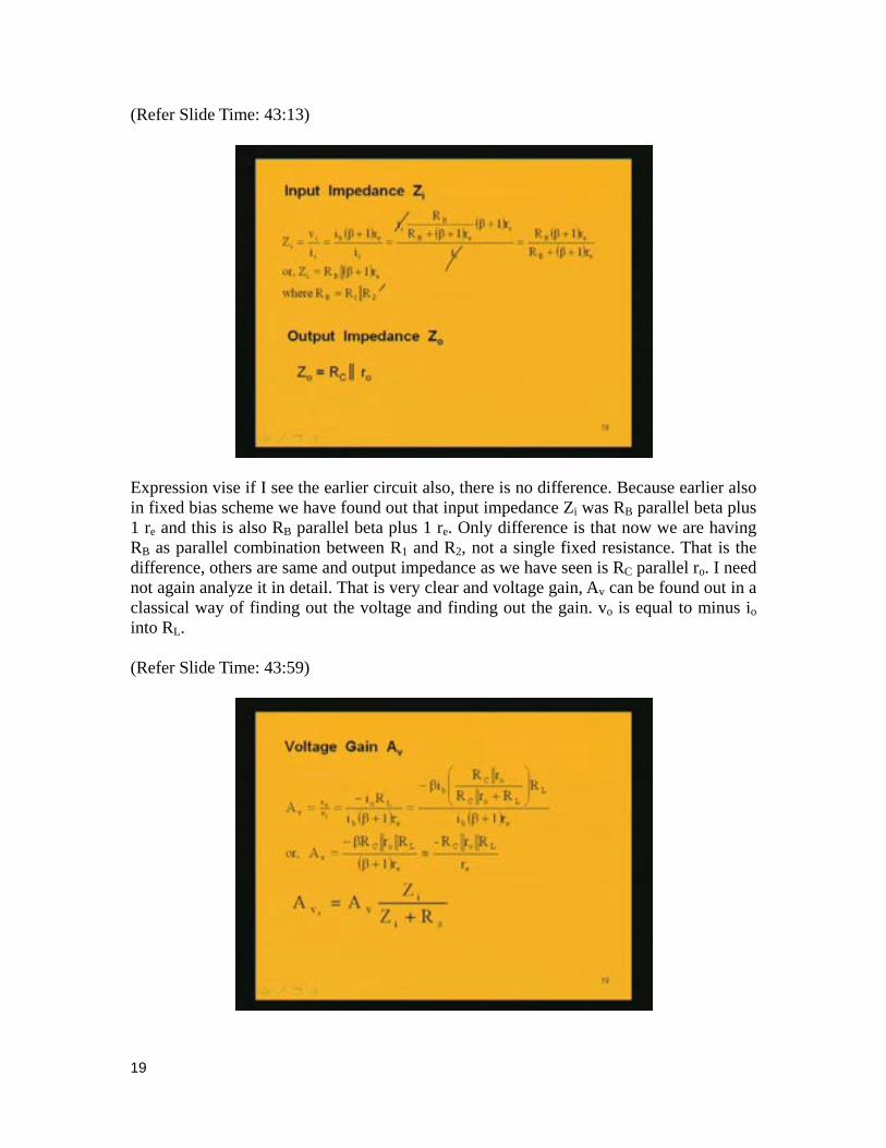
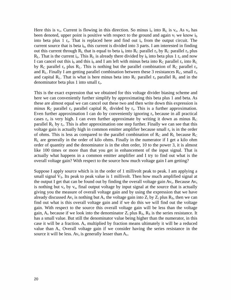
Expression vise if I see the earlier circuit also, there is no difference. Because earlier also in fixed bias scheme we have found out that input impedance Zi was RB parallel beta plus 1 re and this is also RB parallel beta plus 1 re. Only difference is that now we are having RB as parallel combination between R1 and R2, not a single fixed resistance. That is the difference, others are same and output impedance as we have seen is RC parallel ro. I need not again analyze it in detail. That is very clear and voltage gain, Av can be found out in a classical way of finding out the voltage and finding out the gain. vo is equal to minus io into RL. (Refer Slide Time: 43:59)
19
Here this is vo. Current is flowing in this direction. So minus io into RL is vo. As vo has been denoted, upper point is positive with respect to the ground and again vi we know ib into beta plus 1 re. That is replaced here and find out io from the output circuit. The current source that is beta ib, this current is divided into 3 parts. I am interested in finding out this current through RL that is equal to beta ib into RC parallel ro by RC parallel ro plus RL. That is the current io. This RL is already there divided by ib into beta plus 1 re and now I can cancel out this ib and this ib and I am left with minus beta into RC parallel ro into RL by RC parallel ro plus RL. This is nothing but the parallel combination of RC parallel ro and RL. Finally I am getting parallel combination between these 3 resistances RC, small ro and capital RL. That is what is here minus beta into RC parallel ro parallel RL and in the denominator beta plus 1 into small re. This is the exact expression that we obtained for this voltage divider biasing scheme and here we can conveniently further simplify by approximating this beta plus 1 and beta. As these are almost equal we can cancel out these two and then write down this expression is minus RC parallel ro parallel capital RL divided by re. This is a further approximation. Even further approximation I can do by conveniently ignoring ro because in all practical cases ro is very high. I can even further approximate by writing it down as minus RC parallel RL by re. This is after approximation one step further. Finally we can see that this voltage gain is actually high in common emitter amplifier because small re is in the order of ohms. This is less as compared to the parallel combination of RC and RL because RC RL are generally in the order of kilo ohms. Finally in the numerator if I get a kilo ohm order of quantity and the denominator is in the ohm order, 10 to the power 3, it is almost like 100 times or more than that you get in enhancement of the input signal. That is actually what happens in a common emitter amplifier and I try to find out what is the overall voltage gain? With respect to the source how much voltage gain I am getting? Suppose I apply source which is in the order of 1 millivolt peak to peak. I am applying a small signal VS. Its peak to peak value is 1 millivolt. Then how much amplified signal at the output I get that can be found out by finding the overall voltage gain Avs. Because Avs is nothing but vo by vs, final output voltage by input signal at the source that is actually giving you the measure of overall voltage gain and by using the expression that we have already discussed Avs is nothing but Av the voltage gain into Zi by Zi plus RS, then we can find out what is this overall voltage gain and if we do this we will find out the voltage gain. With respect to the source this overall voltage gain will be less than the voltage gain, Av because if we look into the denominator Zi plus RS, RS is the series resistance. It has a small value. But still the denominator value being higher than the numerator, in this case it will be a fraction. Av multiplied by fraction means ultimately it will be a reduced value than Av. Overall voltage gain if we consider having the series resistance in the source it will be less. Avs is generally lesser than Av.
20
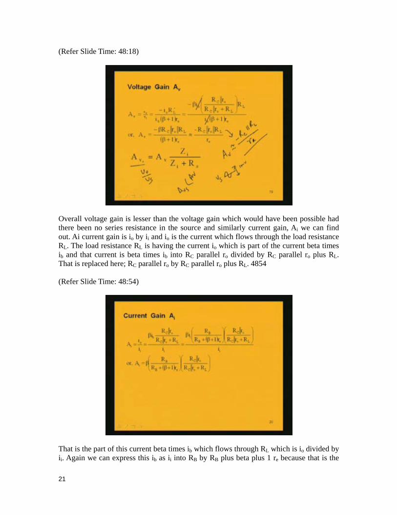
(Refer Slide Time: 48:18)
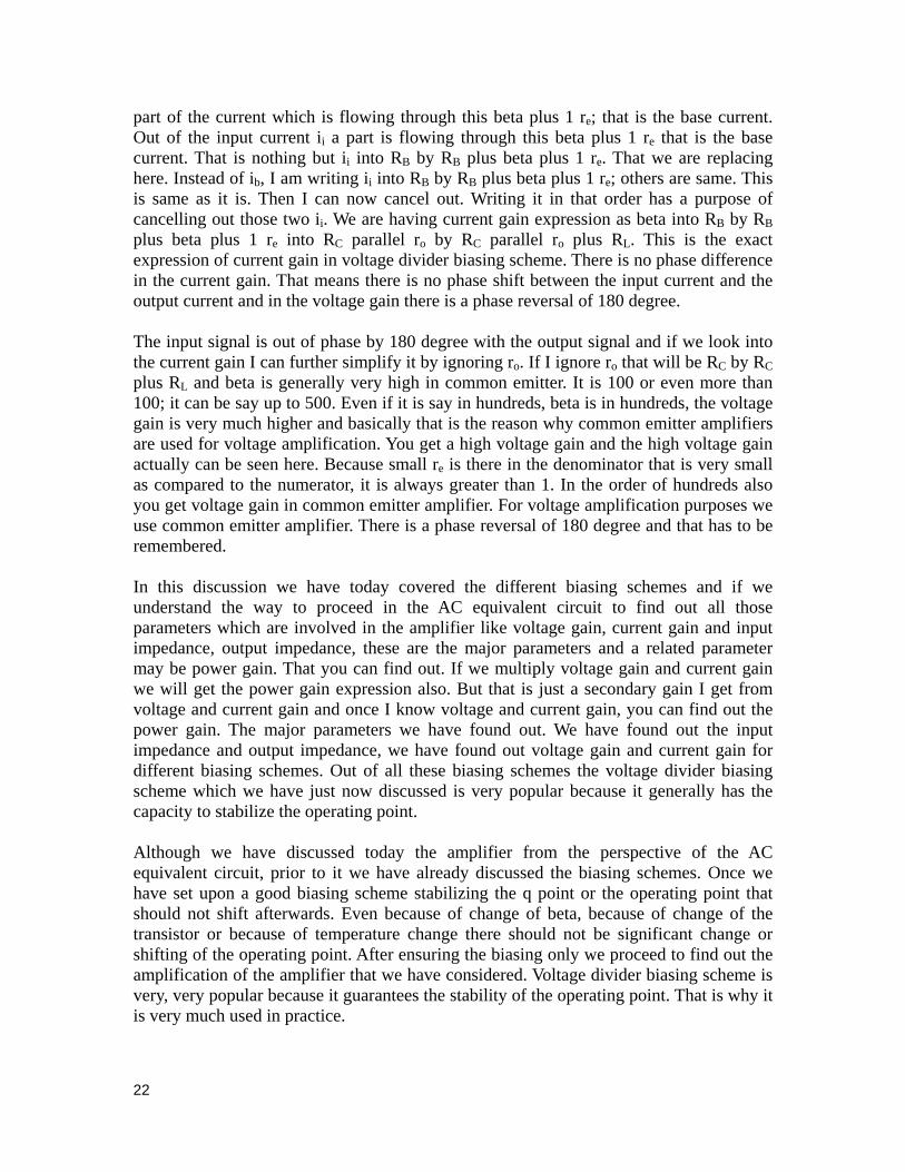
Overall voltage gain is lesser than the voltage gain which would have been possible had there been no series resistance in the source and similarly current gain, Ai we can find out. Ai current gain is io by ii and io is the current which flows through the load resistance RL. The load resistance RL is having the current io which is part of the current beta times ib and that current is beta times ib into RC parallel ro divided by RC parallel ro plus RL. That is replaced here; RC parallel ro by RC parallel ro plus RL. 4854 (Refer Slide Time: 48:54)
That is the part of this current beta times ib which flows through RL which is io divided by ii. Again we can express this ib as ii into RB by RB plus beta plus 1 re because that is the
21
part of the current which is flowing through this beta plus 1 re; that is the base current. Out of the input current ii a part is flowing through this beta plus 1 re that is the base current. That is nothing but ii into RB by RB plus beta plus 1 re. That we are replacing here. Instead of ib, I am writing ii into RB by RB plus beta plus 1 re; others are same. This is same as it is. Then I can now cancel out. Writing it in that order has a purpose of cancelling out those two ii. We are having current gain expression as beta into RB by RB plus beta plus 1 re into RC parallel ro by RC parallel ro plus RL. This is the exact expression of current gain in voltage divider biasing scheme. There is no phase difference in the current gain. That means there is no phase shift between the input current and the output current and in the voltage gain there is a phase reversal of 180 degree. The input signal is out of phase by 180 degree with the output signal and if we look into the current gain I can further simplify it by ignoring ro. If I ignore ro that will be RC by RC plus RL and beta is generally very high in common emitter. It is 100 or even more than 100; it can be say up to 500. Even if it is say in hundreds, beta is in hundreds, the voltage gain is very much higher and basically that is the reason why common emitter amplifiers are used for voltage amplification. You get a high voltage gain and the high voltage gain actually can be seen here. Because small re is there in the denominator that is very small as compared to the numerator, it is always greater than 1. In the order of hundreds also you get voltage gain in common emitter amplifier. For voltage amplification purposes we use common emitter amplifier. There is a phase reversal of 180 degree and that has to be remembered. In this discussion we have today covered the different biasing schemes and if we understand the way to proceed in the AC equivalent circuit to find out all those parameters which are involved in the amplifier like voltage gain, current gain and input impedance, output impedance, these are the major parameters and a related parameter may be power gain. That you can find out. If we multiply voltage gain and current gain we will get the power gain expression also. But that is just a secondary gain I get from voltage and current gain and once I know voltage and current gain, you can find out the power gain. The major parameters we have found out. We have found out the input impedance and output impedance, we have found out voltage gain and current gain for different biasing schemes. Out of all these biasing schemes the voltage divider biasing scheme which we have just now discussed is very popular because it generally has the capacity to stabilize the operating point. Although we have discussed today the amplifier from the perspective of the AC equivalent circuit, prior to it we have already discussed the biasing schemes. Once we have set upon a good biasing scheme stabilizing the q point or the operating point that should not shift afterwards. Even because of change of beta, because of change of the transistor or because of temperature change there should not be significant change or shifting of the operating point. After ensuring the biasing only we proceed to find out the amplification of the amplifier that we have considered. Voltage divider biasing scheme is very, very popular because it guarantees the stability of the operating point. That is why it is very much used in practice.
22
With the voltage divider biasing scheme along with those capacitances which are coupling capacitances and by pass capacitance we have found out all the parameters which are involved in the amplifier. We can find out for any biasing scheme if we proceed in a similar way from the starting principle. In order to find out the voltage gain we must proceed from the starting point which is nothing but the ratio between the output voltage and input voltage. What is output voltage, what is input voltage? Those expressions we have to find out keeping in mind the AC equivalent circuit or referring to the AC equivalent circuit along with the transistor model being incorporated into it. We can find out any parameter for any biasing scheme amplifier proceeding in the same manner which we discussed today and even if some of the resistances are absent; for example we have no resistances in the emitter. That is emitter is having no resistance. In this circuit if there is no resistance in this emitter or simply it is connected to ground, then also we can find out. By proceeding from the first principle, there is no difficulty in finding out the parameters for any circuit with even some of the resistances being not there; instead of 2 there is only 1 single resistance as we discussed in the first case. Always we have to proceed with the first principle. That means if we want to find out the input impedance it will be vi by ii. But one thing to be noted here is that we will be considering the source and a load outside the purview of this two terminal network. That means input terminals will have the source resistances and the source outside and the output terminal will have the load resistance outside. This point has to be remembered and the whole network will be in between these two points or two pair of terminals, input and output; 1 1 dash and 2 2 dash, if we name it. (Refer Slide Time: 56:03)
In that way we can proceed and find out the parameters which are required or which are important for this amplifier and we can find out for any of the configurations. Basically if we are asked to find out the voltage gain of this particular amplifier, then by plugging in all the values we can find out the gain.
23
Next we will consider the numerical example. If I want to find out numerically the value of any of the parameters for any of the configuration we can do that. Today’s discussion actually leads us to going a step further for exactly finding out the amplifier parameters. But we have to keep in mind that we are still considering the small signal analysis. Our signal is still small enough to make the transistor operate in active region only. The transistor should not be overdriven into either saturation or cutoff. These two conditions should never arise. Then only this whole discussion is valid. Whatever small signal analysis we are doing, we are applying it to the transistor amplifier and in view of this small signal being applied we are still in the active reason or the transistor is operating in the active region. That is why we can write down that ic is equal to beta times ib. If it is saturation we will never be able to analyze it in the way that we are analyzing. This point has to be kept in mind that we are dealing with a small signal analysis and we are trying to find out all those parameters involved in the amplifier taking example of different biasing schemes and finding out all this. Today we discussed about common emitter transistor amplifier, BJT common emitter configuration with different biasing schemes. Also there are common base and common collector amplifiers and these common base and common emitter amplifiers are basically used for some difficult, special applications; like a voltage buffer or current buffer, etc, it will be used. We will discuss that but then today we have discussed about the most frequently or commonly used amplifier for voltage amplification and in that case generally the common emitter amplifier is used. We have discussed extensively about common emitter amplifier in different configurations of biasing. We will also discuss about common base and common collector amplifiers next.