62
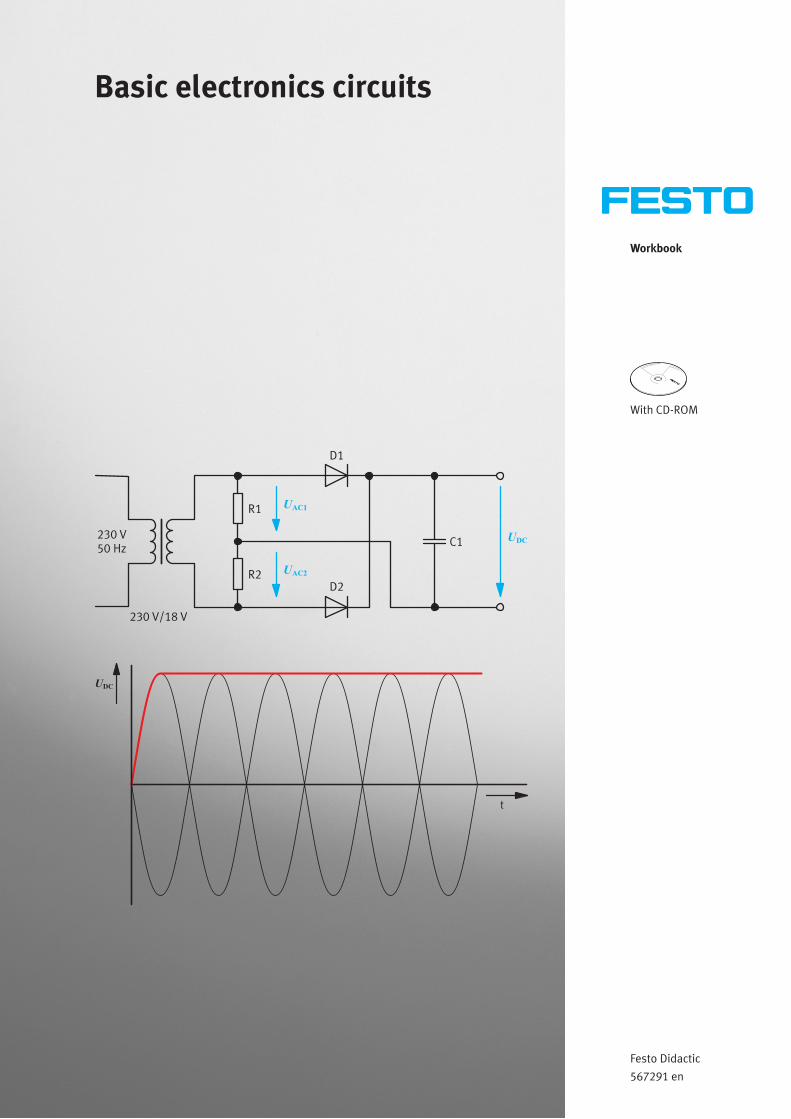
Workbook With CD-ROM Festo Didactic 567291 en Basic electronics circuits C1 230 V/18 V D1 230 V 50 Hz U DC R1 R2 U AC1 U AC2 D2 U DC t
| Date post: | 29-Jan-2023 |
| Category: |
Documents |
| Upload: | khangminh22 |
| View: | 0 times |
| Download: | 0 times |
Workbook
With CD-ROM
Festo Didactic
567291 en
Basic electronics circuits
C1
230 V/18 V
D1
230 V
50 HzUDC
R1
R2
UAC1
UAC2
D2
UDC
t

Order no. 567291
Revision level: 09/2011
Author: Karl-Heinz Drüke
Editor: Frank Ebel
Graphics: Anika Kuhn, Thomas Ocker, Doris Schwarzenberger
Layout: 12/2011, Frank Ebel, Beatrice Huber
© Festo Didactic SE, D-73770 Denkendorf, Germany, 2015
All rights reserved.
Internet: www.festo-didactic.com
e-mail: [email protected]
The purchaser shall receive a single right of use which is non-exclusive, non-time-limited and limited
geographically to use at the purchaser's site/location as follows.
The purchaser shall be entitled to use the work to train his/her staff at the purchaser's site/location and
shall also be entitled to use parts of the copyright material as the basis for the production of his/her own
training documentation for the training of his/her staff at the purchaser's site/location with
acknowledgement of source and to make copies for this purpose. In the case of schools/technical colleges
and training centres, the right of use shall also include use by school and college students and trainees at
the purchaser's site/location for teaching purposes.
The right of use shall in all cases exclude the right to publish the copyright material or to make this available
for use on intranet, Internet and LMS platforms and databases such as Moodle, which allow access by a
wide variety of users, including those outside of the purchaser's site/location.
Entitlement to other rights relating to reproductions, copies, adaptations, translations, microfilming and
transfer to and storage and processing in electronic systems, no matter whether in whole or in part, shall
require the prior consent of Festo Didactic.
© Festo Didactic 567291 III
Table of Contents
Intended use ______________________________________________________________________________ IV
Preface _________________________________________________________________________________ V
Introduction ______________________________________________________________________________ VII
Work and safety instructions _______________________________________________________________ VIII
Training package – Fundamentals of electrical engineering/electronics (TP 1011) ___________________ IX
Allocation of learning objectives to exercises – basic electronic circuits ______________________________ X
Equipment set ____________________________________________________________________________ XIII
Allocation of components to exercises – basic electronic circuits _________________________________ XVIII
Notes for the teacher/trainer _________________________________________________________________ XX
Structure of the exercises __________________________________________________________________ XXI
Component designations ___________________________________________________________________ XXI
Contents of the CD-ROM ___________________________________________________________________ XXII
Exercises and solutions
Exercise 1: Examining characteristic values of transistors _________________________________________ 3
Exercise 2: Differentiating basic transistor circuits ______________________________________________ 21
Exercise 3: Examining multistage amplifiers ___________________________________________________ 39
Exercise 4: Setting up a power amplifier ______________________________________________________ 57
Exercise 5: Amplifying direct voltage signals___________________________________________________ 73
Exercise 6: Generating pulse voltage and sawtooth voltage ______________________________________ 91
Exercise 7: Setting up sine-wave generators with LC and RC elements ____________________________ 111
Exercise 8: Examining power pack circuits ___________________________________________________ 129
Exercise 9: Becoming familiar with DC voltage converters _______________________________________ 147
Exercise 10: Using thyristors and triacs _______________________________________________________ 163
Exercises and worksheets
Exercise 1: Examining characteristic values of transistors _________________________________________ 3
Exercise 2: Differentiating basic transistor circuits ______________________________________________ 21
Exercise 3: Examining multistage amplifiers ___________________________________________________ 39
Exercise 4: Setting up a power amplifier ______________________________________________________ 57
Exercise 5: Amplifying direct voltage signals___________________________________________________ 73
Exercise 6: Generating pulse voltage and sawtooth voltage ______________________________________ 91
Exercise 7: Setting up sine-wave generators with LC and RC elements ____________________________ 111
Exercise 8: Examining power pack circuits ___________________________________________________ 129
Exercise 9: Becoming familiar with DC voltage converters _______________________________________ 147
Exercise 10: Using thyristors and triacs _______________________________________________________ 163
IV © Festo Didactic 567291
Use for intended purpose
The training package for “Basic principles of electrical engineering/electronics” may only be used:
• For its intended purpose in teaching and training applications
• When its safety functions are in flawless condition
The components included in the training package are designed in accordance with the latest technology as
well as recognised safety rules. However, life and limb of the user and third parties may be endangered, and
the components may be impaired, if they are used incorrectly.
The learning system from Festo Didactic has been developed and produced exclusively for training and
further education in the field of automation technology. The training companies and/or trainers must ensure
that all trainees observe the safety instructions described in this workbook.
Festo Didactic hereby excludes any and all liability for damages suffered by trainees, the training company
and/or any third parties, which occur during use of the equipment sets in situations which serve any
purpose other than training and/or vocational education, unless such damages have been caused by Festo
Didactic due to malicious intent or gross negligence.
© Festo Didactic 567291 V
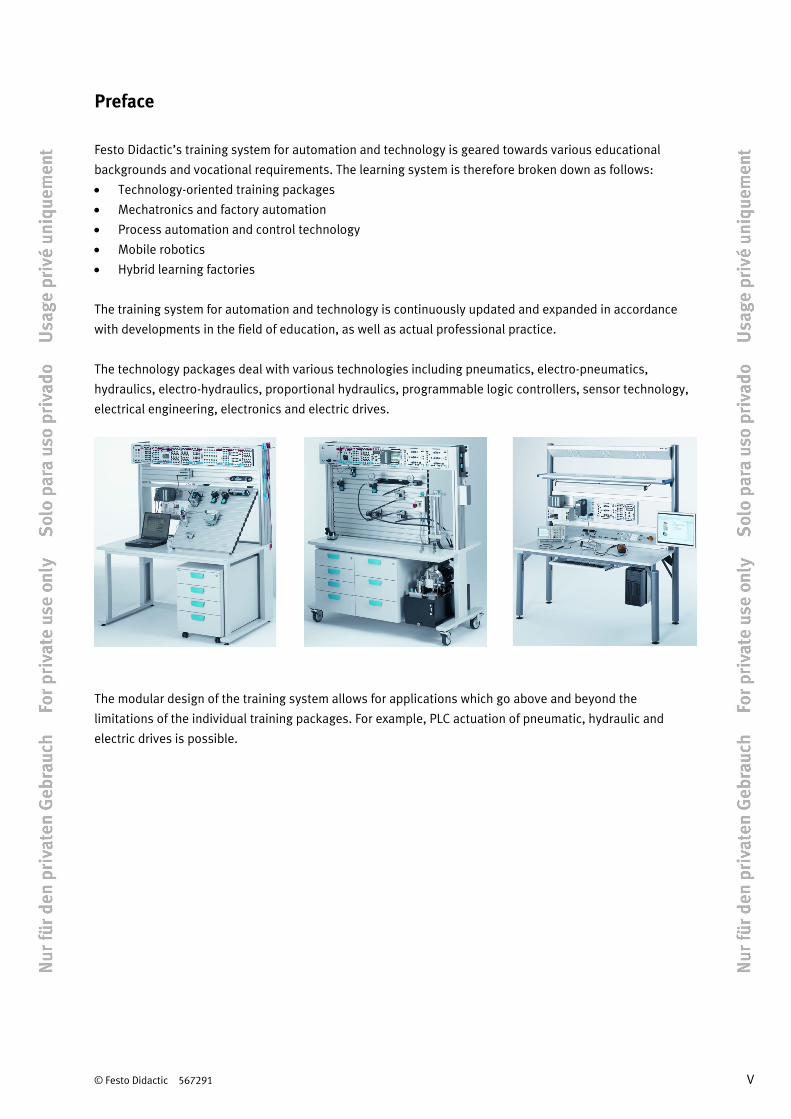
Preface
Festo Didactic’s training system for automation and technology is geared towards various educational
backgrounds and vocational requirements. The learning system is therefore broken down as follows:
• Technology-oriented training packages
• Mechatronics and factory automation
• Process automation and control technology
• Mobile robotics
• Hybrid learning factories
The training system for automation and technology is continuously updated and expanded in accordance
with developments in the field of education, as well as actual professional practice.
The technology packages deal with various technologies including pneumatics, electro-pneumatics,
hydraulics, electro-hydraulics, proportional hydraulics, programmable logic controllers, sensor technology,
electrical engineering, electronics and electric drives.
The modular design of the training system allows for applications which go above and beyond the
limitations of the individual training packages. For example, PLC actuation of pneumatic, hydraulic and
electric drives is possible.

VI © Festo Didactic 567291
All training packages feature the following elements:
• Hardware
• Media
• Seminars
Hardware
The hardware in the training packages is comprised of industrial components and systems that are specially
designed for training purposes. The components contained in the training packages are specifically
designed and selected for the projects in the accompanying media.
Media
The media provided for the individual topics consist of a mixture of courseware and software. The
courseware includes:
• Technical literature and textbooks (standard works for teaching basic knowledge)
• Workbooks (practical exercises with supplementary instructions and sample solutions)
• Lexicons, manuals and technical books (which provide technical information on groups of topics for
further exploration)
• Transparencies and videos (for easy-to-follow, dynamic instruction)
• Posters (for presenting information in a clear-cut way)
Within the software, the following programmes are available:
• Digital training programmes (learning content specifically designed for virtual training)
• Simulation software
• Visualisation software
• Software for acquiring measurement data
• Project engineering and design engineering software
• Programming software for programmable logic controllers
The teaching and learning media are available in several languages. They are intended for use in classroom
instruction, but are also suitable for self-study.
Seminars
A wide range of seminars covering the contents of the training packages round off the system for training
and vocational education.
Do you have suggestions or criticism regarding this manual?
If so, send us an e-mail at [email protected].
The authors and Festo Didactic look forward to your comments.
© Festo Didactic 567291 VII
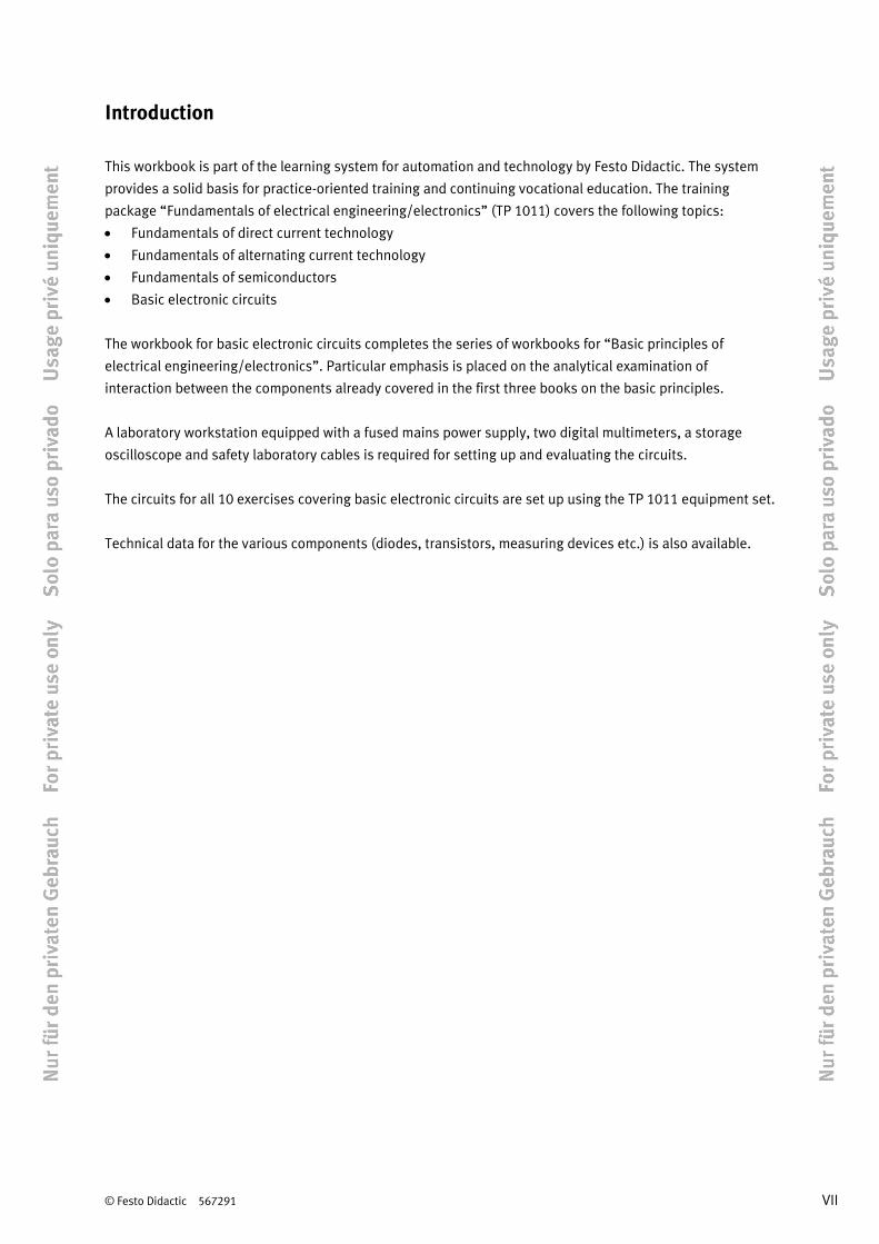
Introduction
This workbook is part of the learning system for automation and technology by Festo Didactic. The system
provides a solid basis for practice-oriented training and continuing vocational education. The training
package “Fundamentals of electrical engineering/electronics” (TP 1011) covers the following topics:
• Fundamentals of direct current technology
• Fundamentals of alternating current technology
• Fundamentals of semiconductors
• Basic electronic circuits
The workbook for basic electronic circuits completes the series of workbooks for “Basic principles of
electrical engineering/electronics”. Particular emphasis is placed on the analytical examination of
interaction between the components already covered in the first three books on the basic principles.
A laboratory workstation equipped with a fused mains power supply, two digital multimeters, a storage
oscilloscope and safety laboratory cables is required for setting up and evaluating the circuits.
The circuits for all 10 exercises covering basic electronic circuits are set up using the TP 1011 equipment set.
Technical data for the various components (diodes, transistors, measuring devices etc.) is also available.
VIII © Festo Didactic 567291
Work and safety instructions
General information
• Trainees should only work with the circuits under the supervision of a trainer.
• Observe specifications included in the technical data for the individual components, and in particular all
safety instructions!
• Malfunctions which may impair safety must not be generated in the training environment and must be
eliminated immediately.
Electrical components
• Risk of death in case of interrupted protective earth conductor!
– The protective earth conductor (yellow/green) must never be interrupted, either inside or outside a
device.
– The insulation of the protective earth conductor must never be damaged or removed.
• German trade association regulations BGV A3, “Electrical systems and equipment”, must be observed in
commercial facilities.
• In schools and training facilities, the operation of power supply units must be responsibly monitored by
trained personnel.
• Caution!
The capacitors in the device may still carry a charge even after it has been disconnected from all power
sources.
• When replacing fuses, use specified fuses only with the correct current rating.
• Never switch the power supply unit on immediately after it has been moved from a cold room to a warm
room. Under unfavourable conditions, the condensate which forms as a result may damage the device.
Leave the device switched off until it has reached room temperature.
• Use only extra-low voltage (max. 25 V DC) as the operating voltage for the circuits in the various
exercises.
• Electrical connections may only be established in the absence of voltage.
• Electrical connections may only be interrupted in the absence of voltage.
• Use only connecting cables with safety plugs for electrical connections.
• Always pull the safety plug when disconnecting connecting cables – never pull the cable.
© Festo Didactic 567291 IX
Training package – Fundamentals of electrical engineering/electronics (TP 1011)
Training package TP 1011 consists of a multitude of training materials. The subject of this part of the
TP 1011 training package is basic electronic circuits. Individual components included in training package
TP 1011 may also be included in other packages.
Important components of TP 1011
• Permanent workstation with EduTrainer® universal patch panel
• Component set for electrical engineering/electronics with jumper plugs and safety laboratory cables
• EduTrainer® basic power supply unit
• Complete set of laboratory equipment
Media
The courseware for training package TP 1011 consists of four workbooks. The workbooks include exercise
sheets for each exercise, the solutions to each individual worksheet and a CD-ROM. A set of ready-to-use
exercise sheets and worksheets is included in each workbook for all of the exercises.
Data sheets for the hardware components are made available along with the training package, and on the
CD-ROM.
Media
Workbooks Fundamentals of direct current technology
Fundamentals of alternating current technology
Fundamentals of semiconductors
Basic electronic circuits
Digital training programmes WBT Electrical engineering 1 – Fundamentals of electrical engineering
WBT Electrical engineering 2 – Direct and alternating current circuits
WBT Electronics 1 – Fundamentals of semiconductor technology
WBT Electronics 2 – Integrated circuits
WBT Electrical protective measures
Overview of media for training package TP 1011
Digital learning programmes available for training package TP 1011 include Electrical engineering 1,
Electrical engineering 2, Electronics 1, Electronics 2 and Electrical protective measures. These programmes
explore the basic principles of electrical engineering/electronics in detail. Training content is elucidated on
the basis of practical case studies in a systematic, applications-oriented fashion.
The media are offered in several languages. You can find further training materials in our catalogue and on
the Internet.
X © Festo Didactic 567291
Allocation of learning objectives to exercises – basic electronic circuits
Exercise 1: Characteristic values of transistors
• You learn to test transistors for correct functioning.
• You learn to ascertain current amplification B for transistors.
• You become familiar with typical current amplification values for transistors.
• You learn to convert circuits for NPN transistors into circuits for PNP transistors.
• You learn to ascertain a circuit’s voltage amplification.
• You become familiar with the effects of operating point adjustments.
• You become familiar with the effects of overdriving an amplifier.
Exercise 2: Basic transistor circuits
• You become familiar with the difference between an emitter follower and a common emitter circuit.
• You become familiar with the three basic transistor circuits.
• You learn to measure voltage amplification in transistor circuits.
• You become familiar with typical voltage amplification in basic transistor circuits.
• You know which basic transistor circuit causes a 180° phase shift.
• You know which basic transistor circuits are non-inverting.
• You learn to specify typical input and output resistance for the basic circuits.
• You learn to measure input and output resistance at amplification circuits.
Exercise 3: Multistage amplifiers
• You learn what a Darlington circuit is.
• You become familiar with complementary Darlington circuit.
• You learn to measure current in the nano-ampere range.
• You know what inverse feedback is.
• You learn to programme amplification gain with two resistors.
• You learn to generate measurement signals in the millivolt range.
• You learn to record an amplifier’s frequency response.
• You learn to ascertain an amplifier’s cut-off frequency.

© Festo Didactic 567291 XI
Exercise 4: Power amplifier
• You become familiar with operating point adjustment is circuits with positive and negative operating
voltage.
• You learn to recognise inverse feedback.
• You learn which components determine a circuit’s amplification gain GU.
• You learn to recognise whether a given amplifier is a power amplifier or a voltage amplifier.
• You learn to recognise a push-pull output stage.
• You learn what crossover distortion is.
• You learn how inverse feedback effects signal distortion.
• You learn to differentiate between class B operation and class AB operation of an output stage.
• You learn to measure an output stage’s quiescent current without an ammeter.
• You learn to determine an amplifier’s output power.
Exercise 5: Differential and direct voltage amplifiers
• You learn to recognise the typical structure of a basic, differential amplifier circuit.
• You learn to indirectly determine current within circuits.
• You become familiar with the typical characteristics of a differential amplifier.
• You learn to record and draw the two characteristic curves – Uout = f (Uin) – of a differential amplifier.
• You learn the difference between differential amplification und common-mode amplification.
• You learn how to achieve a high common-mode rejection ratio, and where this attribute is necessary.
• You learn to recognise a constant current source/sink, and how to calculate constant current.
• You know what a comparator is.
• You learn to set up a twilight switch and explain its function.
• You learn what self-excitation is and what it does.
• You become familiar with the layout and typical characteristics of a direct voltage amplifier.
• You learn about offset and offset alignment.
Exercise 6: Pulse and sawtooth generators
• You learn to recognise the basic circuit of the classical astable multivibrator (AMV).
• You become familiar with the typical characteristics of an astable multivibrator.
• You become familiar with the characteristics of a trigger circuit.
• You learn to measure and calculate the trigger levels and hysteresis of a trigger circuit.
• You learn to convert a trigger circuit and an RC element into a square-wave generator
• You learn to measure and calculate pulse data for various square-wave generators.
• You learn what pulse-width modulation is (PWM) and how it is used.
• You become familiar with the characteristics of a monostable trigger circuit.
• You learn to measure the capacitance of capacitors.
• You learn to dimension the time-determining elements of various pulse circuits.
• You learn how a unijunction transistor (UJT) works and how to test it.
• You learn to convert curved sawtooth voltages into linearly rising sawtooth voltages.
XII © Festo Didactic 567291
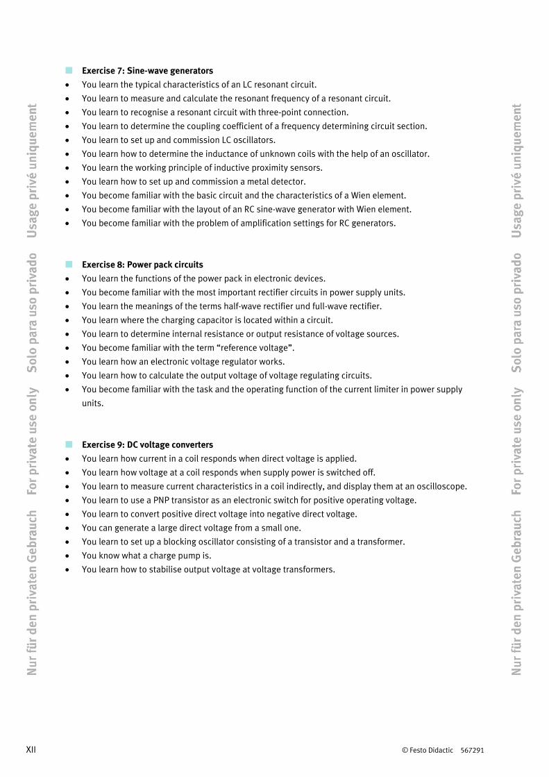
Exercise 7: Sine-wave generators
• You learn the typical characteristics of an LC resonant circuit.
• You learn to measure and calculate the resonant frequency of a resonant circuit.
• You learn to recognise a resonant circuit with three-point connection.
• You learn to determine the coupling coefficient of a frequency determining circuit section.
• You learn to set up and commission LC oscillators.
• You learn how to determine the inductance of unknown coils with the help of an oscillator.
• You learn the working principle of inductive proximity sensors.
• You learn how to set up and commission a metal detector.
• You become familiar with the basic circuit and the characteristics of a Wien element.
• You become familiar with the layout of an RC sine-wave generator with Wien element.
• You become familiar with the problem of amplification settings for RC generators.
Exercise 8: Power pack circuits
• You learn the functions of the power pack in electronic devices.
• You become familiar with the most important rectifier circuits in power supply units.
• You learn the meanings of the terms half-wave rectifier und full-wave rectifier.
• You learn where the charging capacitor is located within a circuit.
• You learn to determine internal resistance or output resistance of voltage sources.
• You become familiar with the term “reference voltage”.
• You learn how an electronic voltage regulator works.
• You learn how to calculate the output voltage of voltage regulating circuits.
• You become familiar with the task and the operating function of the current limiter in power supply
units.
Exercise 9: DC voltage converters
• You learn how current in a coil responds when direct voltage is applied.
• You learn how voltage at a coil responds when supply power is switched off.
• You learn to measure current characteristics in a coil indirectly, and display them at an oscilloscope.
• You learn to use a PNP transistor as an electronic switch for positive operating voltage.
• You learn to convert positive direct voltage into negative direct voltage.
• You can generate a large direct voltage from a small one.
• You learn to set up a blocking oscillator consisting of a transistor and a transformer.
• You know what a charge pump is.
• You learn how to stabilise output voltage at voltage transformers.
© Festo Didactic 567291 XIII
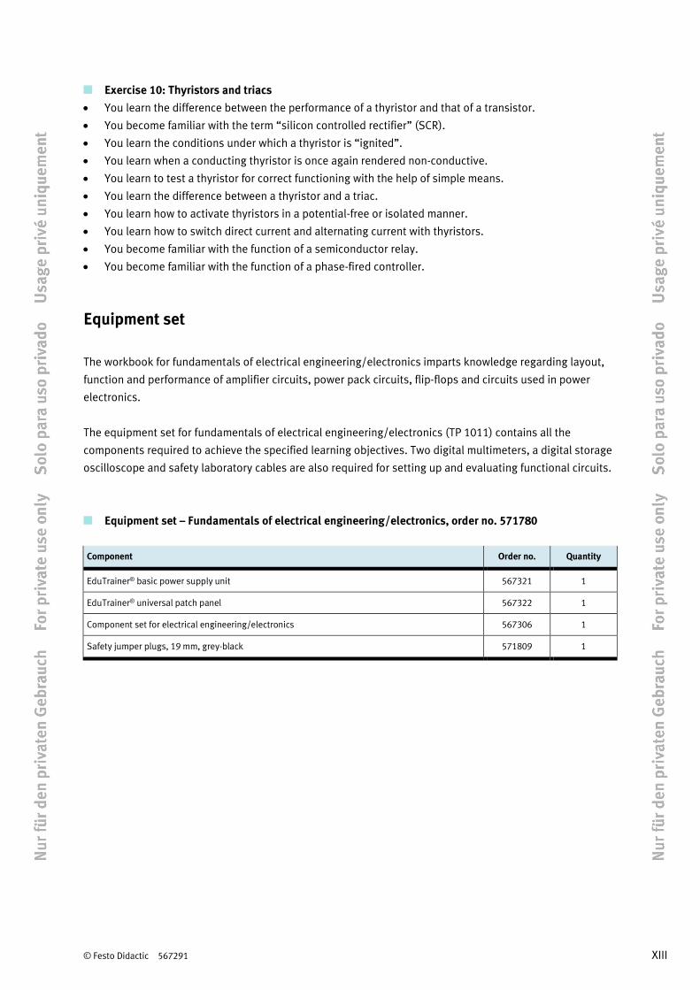
Exercise 10: Thyristors and triacs
• You learn the difference between the performance of a thyristor and that of a transistor.
• You become familiar with the term “silicon controlled rectifier” (SCR).
• You learn the conditions under which a thyristor is “ignited”.
• You learn when a conducting thyristor is once again rendered non-conductive.
• You learn to test a thyristor for correct functioning with the help of simple means.
• You learn the difference between a thyristor and a triac.
• You learn how to activate thyristors in a potential-free or isolated manner.
• You learn how to switch direct current and alternating current with thyristors.
• You become familiar with the function of a semiconductor relay.
• You become familiar with the function of a phase-fired controller.
Equipment set
The workbook for fundamentals of electrical engineering/electronics imparts knowledge regarding layout,
function and performance of amplifier circuits, power pack circuits, flip-flops and circuits used in power
electronics.
The equipment set for fundamentals of electrical engineering/electronics (TP 1011) contains all the
components required to achieve the specified learning objectives. Two digital multimeters, a digital storage
oscilloscope and safety laboratory cables are also required for setting up and evaluating functional circuits.
Equipment set – Fundamentals of electrical engineering/electronics, order no. 571780
Component Order no. Quantity
EduTrainer® basic power supply unit 567321 1
EduTrainer® universal patch panel 567322 1
Component set for electrical engineering/electronics 567306 1
Safety jumper plugs, 19 mm, grey-black 571809 1
XIV © Festo Didactic 567291
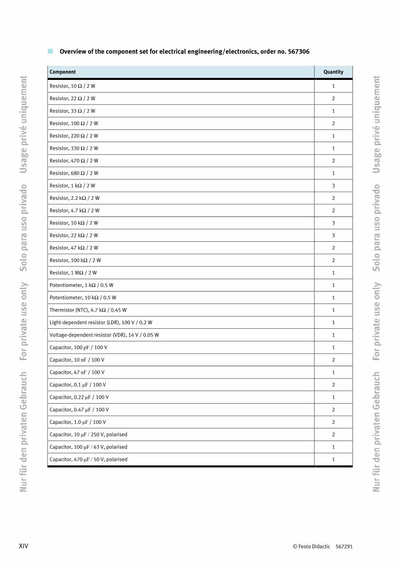
Overview of the component set for electrical engineering/electronics, order no. 567306
Component Quantity
Resistor, 10 Ω / 2 W 1
Resistor, 22 Ω / 2 W 2
Resistor, 33 Ω / 2 W 1
Resistor, 100 Ω / 2 W 2
Resistor, 220 Ω / 2 W 1
Resistor, 330 Ω / 2 W 1
Resistor, 470 Ω / 2 W 2
Resistor, 680 Ω / 2 W 1
Resistor, 1 kΩ / 2 W 3
Resistor, 2.2 kΩ / 2 W 2
Resistor, 4.7 kΩ / 2 W 2
Resistor, 10 kΩ / 2 W 3
Resistor, 22 kΩ / 2 W 3
Resistor, 47 kΩ / 2 W 2
Resistor, 100 kΩ / 2 W 2
Resistor, 1 MΩ / 2 W 1
Potentiometer, 1 kΩ / 0.5 W 1
Potentiometer, 10 kΩ / 0.5 W 1
Thermistor (NTC), 4.7 kΩ / 0.45 W 1
Light-dependent resistor (LDR), 100 V / 0.2 W 1
Voltage-dependent resistor (VDR), 14 V / 0.05 W 1
Capacitor, 100 pF / 100 V 1
Capacitor, 10 nF / 100 V 2
Capacitor, 47 nF / 100 V 1
Capacitor, 0.1 μF / 100 V 2
Capacitor, 0.22 μF / 100 V 1
Capacitor, 0.47 μF / 100 V 2
Capacitor, 1.0 μF / 100 V 2
Capacitor, 10 μF / 250 V, polarised 2
Capacitor, 100 μF / 63 V, polarised 1
Capacitor, 470 μF / 50 V, polarised 1
© Festo Didactic 567291 XV
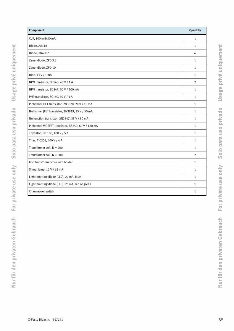
Component Quantity
Coil, 100 mH/50 mA 1
Diode, AA118 1
Diode, 1N4007 6
Zener diode, ZPD 3.3 1
Zener diode, ZPD 10 1
Diac, 33 V / 1 mA 1
NPN transistor, BC140, 40 V / 1 A 2
NPN transistor, BC547, 50 V / 100 mA 1
PNP transistor, BC160, 40 V / 1 A 1
P-channel JFET transistor, 2N3820, 20 V / 10 mA 1
N-channel JFET transistor, 2N3819, 25 V / 50 mA 1
Unijunction transistor, 2N2647, 35 V / 50 mA 1
P-channel MOSFET transistor, BS250, 60 V / 180 mA 1
Thyristor, TIC 106, 400 V / 5 A 1
Triac, TIC206, 400 V / 4 A 1
Transformer coil, N = 200 1
Transformer coil, N = 600 2
Iron transformer core with holder 1
Signal lamp, 12 V / 62 mA 1
Light-emitting diode (LED), 20 mA, blue 1
Light-emitting diode (LED), 20 mA, red or green 1
Changeover switch 1
XVI © Festo Didactic 567291
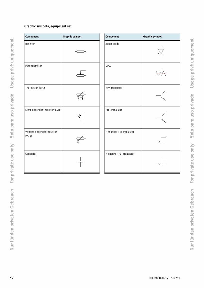
Graphic symbols, equipment set
Component Graphic symbol Component Graphic symbol
Resistor
Zener diode
Potentiometer
DIAC
Thermistor (NTC)
NPN transistor
Light-dependent resistor (LDR)
PNP transistor
Voltage-dependent resistor
(VDR)
U
P-channel JFET transistor
Capacitor
N-channel JFET transistor
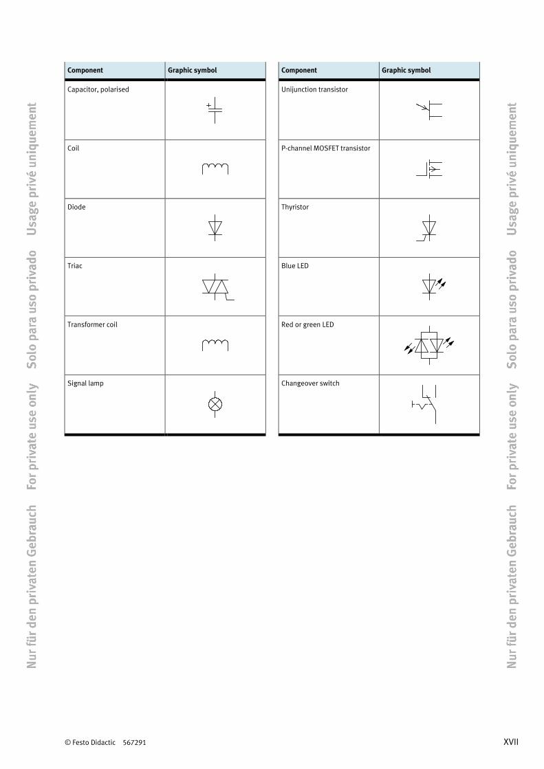
© Festo Didactic 567291 XVII
Component Graphic symbol Component Graphic symbol
Capacitor, polarised
Unijunction transistor
Coil
P-channel MOSFET transistor
Diode
Thyristor
Triac
Blue LED
Transformer coil
Red or green LED
Signal lamp
Changeover switch
XVIII © Festo Didactic 567291
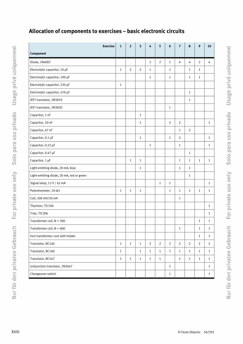
Allocation of components to exercises – basic electronic circuits
Exercise 1 2 3 4 5 6 7 8 9 10
Component
Diode, 1N4007 2 2 1 4 4 2 4
Electrolytic capacitor, 10 µF 1 2 2 1 1 1 1
Electrolytic capacitor, 100 µF 1 1 1 1
Electrolytic capacitor, 220 µF 1
Electrolytic capacitor, 470 µF 1
JFET transistor, 2N3819 1
JFET transistor, 2N3820 1
Capacitor, 1 nF 1
Capacitor, 10 nF 1 2 2 1
Capacitor, 47 nF 1 2
Capacitor, 0.1 µF 1 1 2 1
Capacitor, 0.22 µF 1 1 1
Capacitor, 0.47 µF 1
Capacitor, 1 µF 1 1 1 1 1 1
Light-emitting diode, 20 mA, blue 1 1 1
Light-emitting diode, 20 mA, red or green 1
Signal lamp, 12 V / 62 mA 1 1 1
Potentiometer, 10 kΩ 1 1 1 1 1 1 1 1
Coil, 100 mH/50 mA 1
Thyristor, TIC106 1
Triac, TIC206 1
Transformer coil, N = 200 1 1
Transformer coil, N = 600 1 1 1
Iron transformer core with holder 1 1
Transistor, BC140 1 1 1 2 2 2 2 2 2 2
Transistor, BC160 1 1 1 1 1 1 1 1 1
Transistor, BC547 1 1 1 1 1 1 1 1 1
Unijunction transistor, 2N2647 1 1
Changeover switch 1 1
© Festo Didactic 567291 XIX
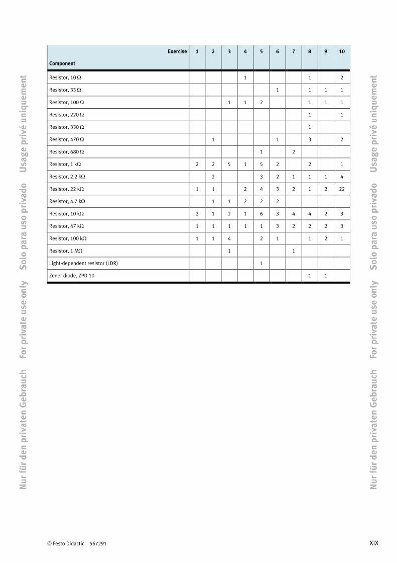
Exercise 1 2 3 4 5 6 7 8 9 10
Component
Resistor, 10 Ω 1 1 2
Resistor, 33 Ω 1 1 1 1
Resistor, 100 Ω 1 1 2 1 1 1
Resistor, 220 Ω 1 1
Resistor, 330 Ω 1
Resistor, 470 Ω 1 1 3 2
Resistor, 680 Ω 1 2
Resistor, 1 kΩ 2 2 5 1 5 2 2 1
Resistor, 2.2 kΩ 2 3 2 1 1 1 4
Resistor, 22 kΩ 1 1 2 4 3 2 1 2 22
Resistor, 4.7 kΩ 1 1 2 2 2
Resistor, 10 kΩ 2 1 2 1 6 3 4 4 2 3
Resistor, 47 kΩ 1 1 1 1 1 3 2 2 2 3
Resistor, 100 kΩ 1 1 4 2 1 1 2 1
Resistor, 1 MΩ 1 1
Light-dependent resistor (LDR) 1
Zener diode, ZPD 10 1 1
XX © Festo Didactic 567291
Notes for the teacher/trainer
Learning objectives
The basic learning goal of this workbook is the setup and analysis of selected basic circuits. Amongst others,
the circuits include power pack circuits, amplifier circuits, flip-flops and circuits used in power electronics.
This direct interplay of theory and practice ensures fast progress and long-lasting learning. Concrete,
individual learning objectives are assigned to each exercise.
Required time
The time required for working through the exercises depends on the learner’s previous knowledge of the
subject matter. Roughly 1 to 1½ hours should be scheduled for each exercise.
Equipment set components
The workbook and the equipment set are designed to be used together. All 10 exercises can be completed
using components from one TP 1011 equipment set.
Standards
The following standards are applied in this workbook:
EN 60617-2 to EN 60617-8 Graphic symbols for diagrams
EN 81346-2 Industrial systems, installations and equipment and industrial products;
structuring principles and reference designations
IEC 60364-1 Low-voltage electrical installations – Fundamental principles,
(DIN VDE 0100-100) Assessment of general characteristics, definitions
IEC 60346-4-41 Low-voltage electrical installations – Protective measures –
(DIN VDE 0100-410) Protection against electric shock
Identification in the workbook
Solutions and supplements in graphics or diagrams appear in red.
Exception: Information and evaluations regarding current are always in red; information and evaluations
regarding voltage are always in blue.
Identification in the worksheets
Texts which require completion are identified with a grid or grey table cells.
Graphics and diagrams which require completion include a grid.
© Festo Didactic 567291 XXI
Solutions
The solutions specified in this workbook result from test measurements. The results of your measurements
may vary from these data.
Learning topics
For the vocation of electrician, the learning topic “basic electronic circuits” is assigned to field of learning 1
of the vocational school.
Structure of the exercises
All 10 exercises have the same structure and are broken down into:
• Title
• Learning objectives
• Problem description
• Circuit or positional sketch
• Project assignment
• Work aids
• Worksheets
The workbook contains the solutions for all exercises.
Component designations
The components in the circuit diagrams are identified in accordance with EN 81346-2. Letters are assigned
as appropriate to each component. Multiple components of the same type within a single circuit are
numbered.
Resistors: R, R1, R2, ...
Capacitors: C, C1, C2, …
Indicators: P, P1, P2, ...
Note
If resistors and capacitors are interpreted as physical variables, the letter identifying them is in
italics (symbols). If digits are required for numbering, they are treated as indices and appear as
subscript.
XXII © Festo Didactic 567291
Contents of the CD-ROM
The workbook is included on the CD-ROM as a PDF file. The CD-ROM also provides you with additional
media.
The CD-ROM contains the following folders:
• Operating instructions
• Illustrations
• Presentations
• Product information
Operating instructions
Operating instructions are provided for various components included in the training package. These
instructions are helpful when using and commissioning the components.
Illustrations
Photos and graphics of components and industrial applications are made available. These can be used to
illustrate individual tasks or to supplement project presentations.
Presentations
This directory contains short presentations for the circuits covered by the training package. These can be
used, for example, to create project presentations.
Product information
Contains product information from the manufacturers of selected components. The representations and
descriptions of the components in this format are intended to show how they would appear in an industrial
catalogue. Additional information regarding the components is also included.

© Festo Didactic 567291 1
Table of contents
Exercises and solutions
Exercise 1: Examining characteristic values of transistors _________________________________________ 3
Exercise 2: Differentiating basic transistor circuits ______________________________________________ 21
Exercise 3: Examining multistage amplifiers ___________________________________________________ 39
Exercise 4: Setting up a power amplifier ______________________________________________________ 57
Exercise 5: Amplifying direct voltage signals___________________________________________________ 73
Exercise 6: Generating pulse voltage and sawtooth voltage ______________________________________ 91
Exercise 7: Setting up sine-wave generators with LC and RC elements ____________________________ 111
Exercise 8: Examining power pack circuits ___________________________________________________ 129
Exercise 9: Becoming familiar with DC voltage converters _______________________________________ 147
Exercise 10: Using thyristors and triacs _______________________________________________________ 163

2 © Festo Didactic 567291
© Festo Didactic 567291 3
Exercise 1 Examining characteristic values of transistors
Learning objectives
After completing this exercise:
• You will know how to test transistors for correct functioning.
• You will be able to ascertain current amplification B for transistors.
• You will be familiar with typical current amplification values for transistors.
• You will know how to convert circuits for NPN transistors into circuits for PNP transistors.
• You will be able to ascertain a circuit’s voltage amplification.
• You will be familiar with the effects of operating point adjustments.
• You will be familiar with the effects of overdriving an amplifier.
Problem description
You work for a company that manufactures and repairs hi-fi amplifiers. During the course of initial training
you will need to familiarise yourself with the performance of transistors and their typical characteristic
values.
You will set up a test circuit to this end, which allows you to determine the degree to which transistors
amplify power. After slightly modifying the circuit, you will then examine how a transistor can be used as a
voltage amplifier.
Exercise 1 – Examining characteristic values of transistors
4 © Festo Didactic 567291
Project assignments
1. Set up a test circuit with NPN transistor BC140 and ascertain the transistor’s power amplification B with
collector current values of IC = 1 mA, 5 mA and 10 mA.
2. For purposes of comparison, determine power amplification B for transistor BC547.
3. Modify the test circuit so that it is suitable for testing PNP transistors, and ascertain power amplification
B for transistor BC160.
4. Set sup a test circuit within which transistors are actuated non-destructively with direct voltage.
Familiarise yourself with the basic principle of voltage amplification.
5. With the help of the test circuit, determine voltage amplification GU when using transistors BC140 and
BC547.
6. Expand the test circuit such that a BC140 transistor can be additionally actuated with alternating
voltage. Familiarise yourself with the concept of alternating voltage amplification.
7. Examine the relationship between operating point setting and output signal distortion.
8. Find out whether the test circuit is a basic common emitter circuit, a basic fundamental circuit or a basic
common collector.
Work aids
• Textbooks, books of tables
• Excerpts from manufacturers’ catalogues
• Data sheets
• Internet
• WBT Electronics 1 and Electronics 2
Exercise 1 – Examining characteristic values of transistors
© Festo Didactic 567291 5
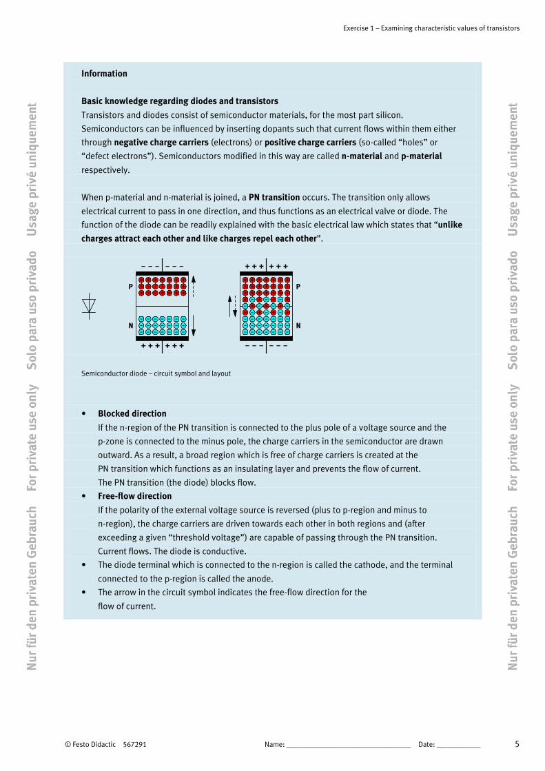
Information
Basic knowledge regarding diodes and transistors
Transistors and diodes consist of semiconductor materials, for the most part silicon.
Semiconductors can be influenced by inserting dopants such that current flows within them either
through negative charge carriers (electrons) or positive charge carriers (so-called “holes” or
“defect electrons”). Semiconductors modified in this way are called n-material and p-material
respectively.
When p-material and n-material is joined, a PN transition occurs. The transition only allows
electrical current to pass in one direction, and thus functions as an electrical valve or diode. The
function of the diode can be readily explained with the basic electrical law which states that “unlike
charges attract each other and like charges repel each other”.
Semiconductor diode – circuit symbol and layout
• Blocked direction
If the n-region of the PN transition is connected to the plus pole of a voltage source and the
p-zone is connected to the minus pole, the charge carriers in the semiconductor are drawn
outward. As a result, a broad region which is free of charge carriers is created at the
PN transition which functions as an insulating layer and prevents the flow of current.
The PN transition (the diode) blocks flow.
• Free-flow direction
If the polarity of the external voltage source is reversed (plus to p-region and minus to
n-region), the charge carriers are driven towards each other in both regions and (after
exceeding a given “threshold voltage”) are capable of passing through the PN transition.
Current flows. The diode is conductive.
• The diode terminal which is connected to the n-region is called the cathode, and the terminal
connected to the p-region is called the anode.
• The arrow in the circuit symbol indicates the free-flow direction for the
flow of current.
Exercise 1 – Examining characteristic values of transistors
6 © Festo Didactic 567291
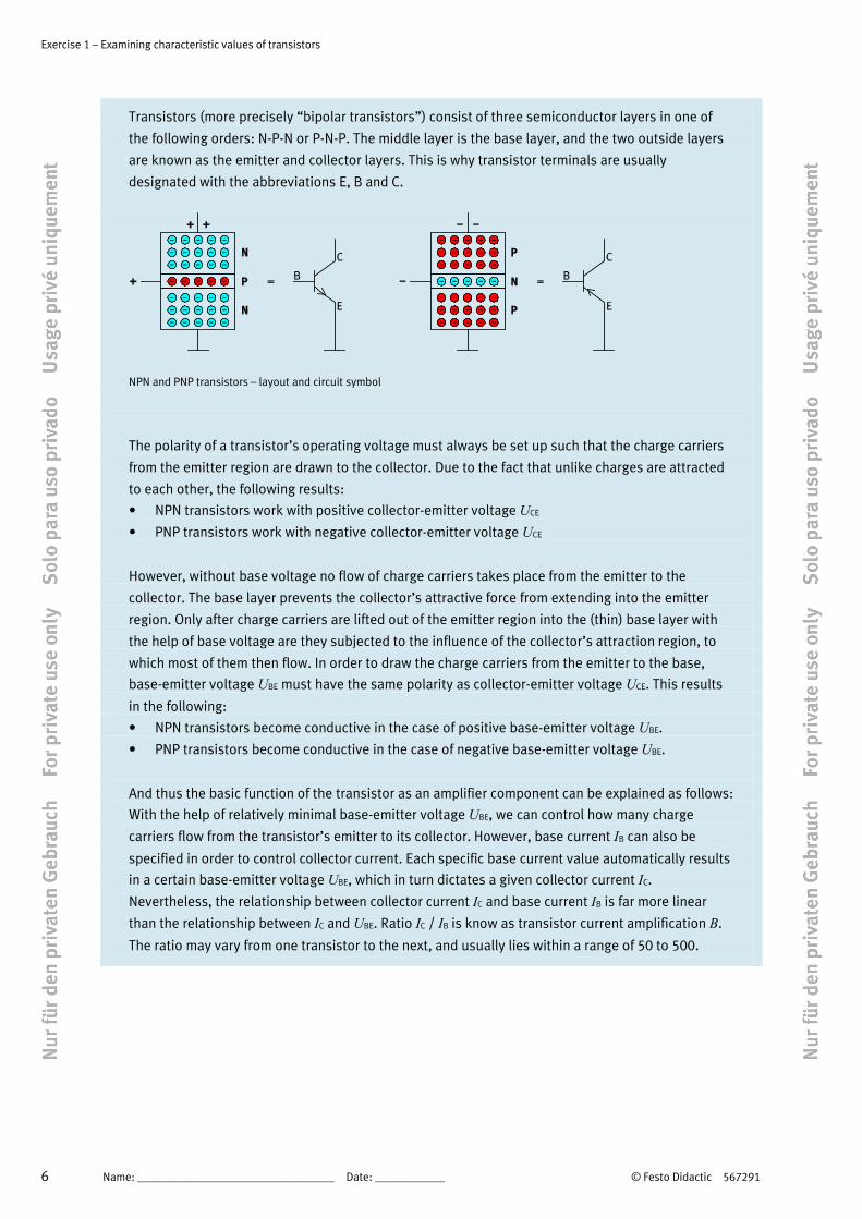
Transistors (more precisely “bipolar transistors”) consist of three semiconductor layers in one of
the following orders: N-P-N or P-N-P. The middle layer is the base layer, and the two outside layers
are known as the emitter and collector layers. This is why transistor terminals are usually
designated with the abbreviations E, B and C.
NPN and PNP transistors – layout and circuit symbol
The polarity of a transistor’s operating voltage must always be set up such that the charge carriers
from the emitter region are drawn to the collector. Due to the fact that unlike charges are attracted
to each other, the following results:
• NPN transistors work with positive collector-emitter voltage UCE
• PNP transistors work with negative collector-emitter voltage UCE
However, without base voltage no flow of charge carriers takes place from the emitter to the
collector. The base layer prevents the collector’s attractive force from extending into the emitter
region. Only after charge carriers are lifted out of the emitter region into the (thin) base layer with
the help of base voltage are they subjected to the influence of the collector’s attraction region, to
which most of them then flow. In order to draw the charge carriers from the emitter to the base,
base-emitter voltage UBE must have the same polarity as collector-emitter voltage UCE. This results
in the following:
• NPN transistors become conductive in the case of positive base-emitter voltage UBE.
• PNP transistors become conductive in the case of negative base-emitter voltage UBE.
And thus the basic function of the transistor as an amplifier component can be explained as follows:
With the help of relatively minimal base-emitter voltage UBE, we can control how many charge
carriers flow from the transistor’s emitter to its collector. However, base current IB can also be
specified in order to control collector current. Each specific base current value automatically results
in a certain base-emitter voltage UBE, which in turn dictates a given collector current IC.
Nevertheless, the relationship between collector current IC and base current IB is far more linear
than the relationship between IC and UBE. Ratio IC / IB is know as transistor current amplification B.
The ratio may vary from one transistor to the next, and usually lies within a range of 50 to 500.
Exercise 1 – Examining characteristic values of transistors
© Festo Didactic 567291 7
The equivalent circuit diagram of a transistor demonstrates its mode of operation in an even
simpler fashion: The transistor’s base-emitter path functions like a diode in the free-flow direction.
Base current IB flowing along this path increases current IC between emitter and collector by a factor
of B. The current source symbol indicates that collector current is for the most part independent of
the collector voltage value.
NPN transistor – equivalent circuit diagram
The emitter is identified with an arrow in the transistor symbol. Regardless of internal processes
within the transistor, the direction of the arrow in the symbol nevertheless represents the actual
direction of flow. The following applies in general to symbols for semiconductor components: The
arrow points either towards a p-region or comes out of an n-region. (mnemonic aid: P = “pointing”
arrow, N = “advancing” arrow).
What does an amplifier do?
The microphone in a telephone converts sound waves created by, for example, speech or music,
into alternating voltage in the millivolt range. However, this signal is too weak to drive a headphone
or a loudspeaker directly. Several volts are required for good, audible reproduction with these
devices. An amplifier must therefore be connected between the microphone and the headphone or
loudspeaker. All amplifiers require (direct) operating voltage in order to generate an output signal.
Amplifier – circuit symbol
In the following pages you will learn how transistor amplifiers work.
Exercise 1 – Examining characteristic values of transistors
8 © Festo Didactic 567291
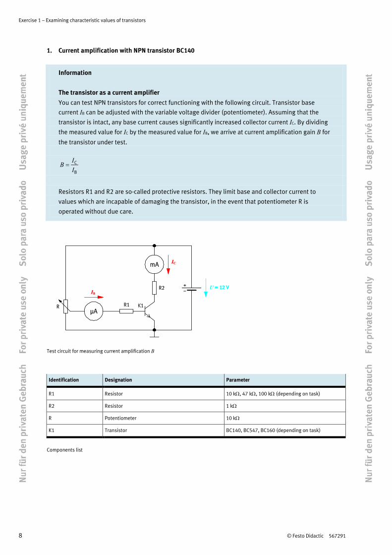
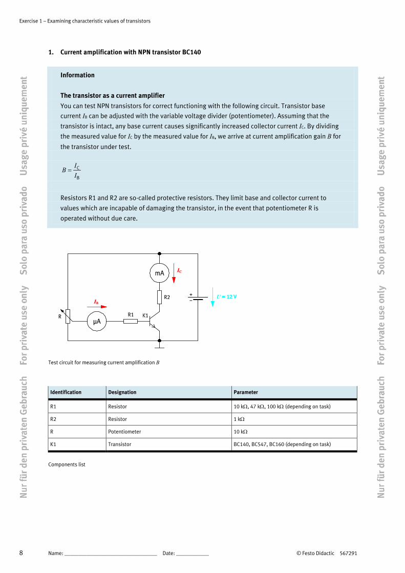
1. Current amplification with NPN transistor BC140
Information
The transistor as a current amplifier
You can test NPN transistors for correct functioning with the following circuit. Transistor base
current IB can be adjusted with the variable voltage divider (potentiometer). Assuming that the
transistor is intact, any base current causes significantly increased collector current IC. By dividing
the measured value for IC by the measured value for IB, we arrive at current amplification gain B for
the transistor under test.
C
B
IBI
=
Resistors R1 and R2 are so-called protective resistors. They limit base and collector current to
values which are incapable of damaging the transistor, in the event that potentiometer R is
operated without due care.
Test circuit for measuring current amplification B
Identification Designation Parameter
R1 Resistor 10 kΩ, 47 kΩ, 100 kΩ (depending on task)
R2 Resistor 1 kΩ
R Potentiometer 10 kΩ
K1 Transistor BC140, BC547, BC160 (depending on task)
Components list
Exercise 1 – Examining characteristic values of transistors
© Festo Didactic 567291 9
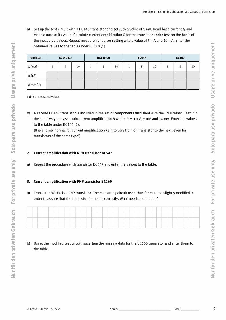
a) Set up the test circuit with a BC140 transistor and set IC to a value of 1 mA. Read base current IB and
make a note of its value. Calculate current amplification B for the transistor under test on the basis of
the measured values. Repeat measurement after setting IC to a value of 5 mA and 10 mA. Enter the
obtained values to the table under BC140 (1).
Transistor BC140 (1) BC140 (2) BC547 BC160
IC [mA] 1 5 10 1 5 10 1 5 10 1 5 10
IB [µA] 7.7 38.5 76.9 8.0 39.8 79.5 3.2 16.1 32.4 4.2 20.8 40.3
B = IC / IB 130 130 130 125 126 126 313 311 308 238 240 248
Table of measured values
b) A second BC140 transistor is included in the set of components furnished with the EduTrainer. Test it in
the same way and ascertain current amplification B where IC = 1 mA, 5 mA and 10 mA. Enter the values
to the table under BC140 (2).
(It is entirely normal for current amplification gain to vary from on transistor to the next, even for
transistors of the same type!)
2. Current amplification with NPN transistor BC547
a) Repeat the procedure with transistor BC547 and enter the values to the table.
3. Current amplification with PNP transistor BC160
a) Transistor BC160 is a PNP transistor. The measuring circuit used thus far must be slightly modified in
order to assure that the transistor functions correctly. What needs to be done?
We only have to reverse operating voltage polarity. If the measuring devices are pointer instruments,
their terminals must be reversed as well. Digital measuring instruments automatically change the
preceding plus or minus signs at their displays.
b) Using the modified test circuit, ascertain the missing data for the BC160 transistor and enter them to
the table.
Exercise 1 – Examining characteristic values of transistors
10 © Festo Didactic 567291
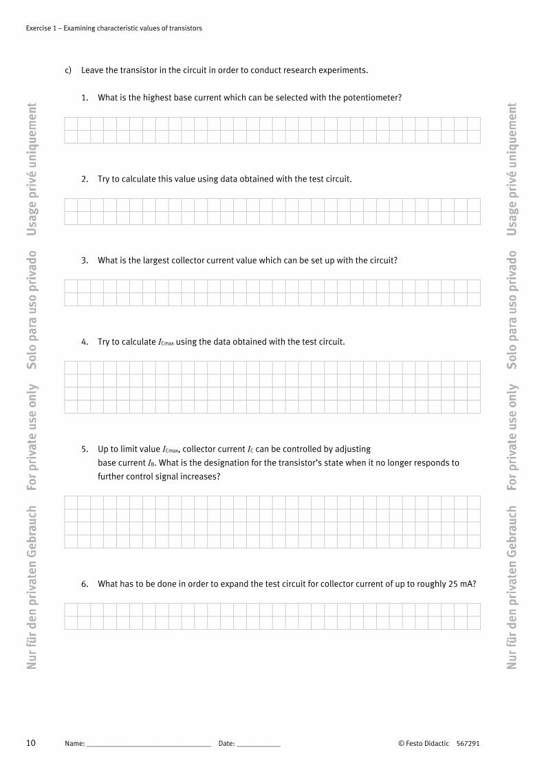
c) Leave the transistor in the circuit in order to conduct research experiments.
1. What is the highest base current which can be selected with the potentiometer?
IBmax = approx. 240 µA
2. Try to calculate this value using data obtained with the test circuit.
Maximum voltage drop at R1 amounts to U – UBE = 12 V – 0.7 V = 11.3 V / 47 kΩ = 240 µA
3. What is the largest collector current value which can be set up with the circuit?
ICmax = approx. 12 mA
4. Try to calculate ICmax using the data obtained with the test circuit.
Maximum voltage drop at R2 amounts to U – UEmin ≈ 12 V – 0 V = 12 V. In this case, current
ICmax = 12 V / 1 kΩ = 12 mA flows through R2 and the series connected transistor.
5. Up to limit value ICmax, collector current IC can be controlled by adjusting
base current IB. What is the designation for the transistor’s state when it no longer responds to
further control signal increases?
We say that the transistor is being overdriven, or has reached a state of saturation.
(It now functions like a switch in the on state. IC is determined by U and R2.)
6. What has to be done in order to expand the test circuit for collector current of up to roughly 25 mA?
R2 must be reduced. R2 = U / ICmax = 12 V / 25 mA = 480 Ω → 470 Ω is selected
Exercise 1 – Examining characteristic values of transistors
© Festo Didactic 567291 11
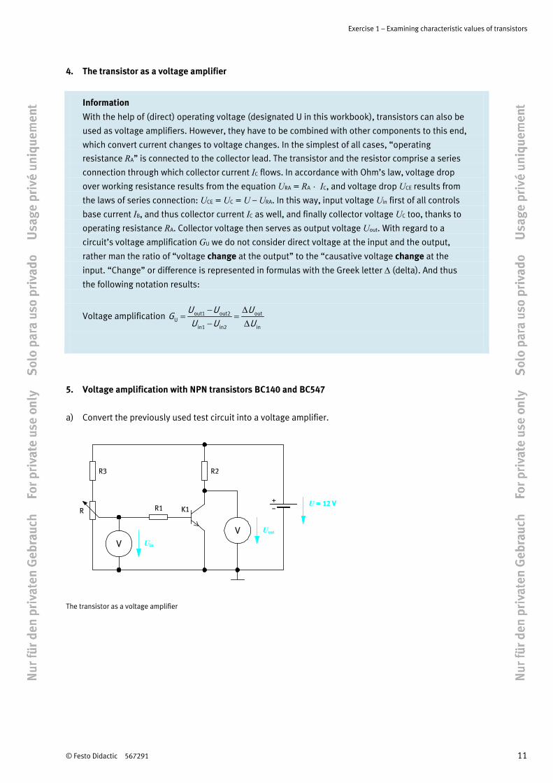
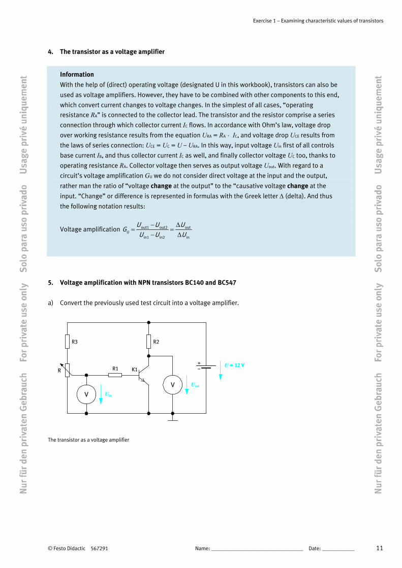
4. The transistor as a voltage amplifier
Information
With the help of (direct) operating voltage (designated U in this workbook), transistors can also be
used as voltage amplifiers. However, they have to be combined with other components to this end,
which convert current changes to voltage changes. In the simplest of all cases, “operating
resistance RA” is connected to the collector lead. The transistor and the resistor comprise a series
connection through which collector current IC flows. In accordance with Ohm’s law, voltage drop
over working resistance results from the equation URA = RA ⋅ IC, and voltage drop UCE results from
the laws of series connection: UCE = UC = U – URA. In this way, input voltage Uin first of all controls
base current IB, and thus collector current IC as well, and finally collector voltage UC too, thanks to
operating resistance RA. Collector voltage then serves as output voltage Uout. With regard to a
circuit’s voltage amplification GU we do not consider direct voltage at the input and the output,
rather man the ratio of “voltage change at the output” to the “causative voltage change at the
input. “Change” or difference is represented in formulas with the Greek letter ∆ (delta). And thus
the following notation results:
Voltage amplification out1 out2 outU
in1 in2 in
U U UG
U U U− ∆
= =− ∆
5. Voltage amplification with NPN transistors BC140 and BC547
a) Convert the previously used test circuit into a voltage amplifier.
The transistor as a voltage amplifier
Exercise 1 – Examining characteristic values of transistors
12 © Festo Didactic 567291
Identification Designation Parameter
R1 Resistor 47 kΩ
R2 Resistor 1 kΩ
R3 Resistor 22 kΩ
R Potentiometer 10 kΩ
K1 Transistor BC140, BC547
Components list
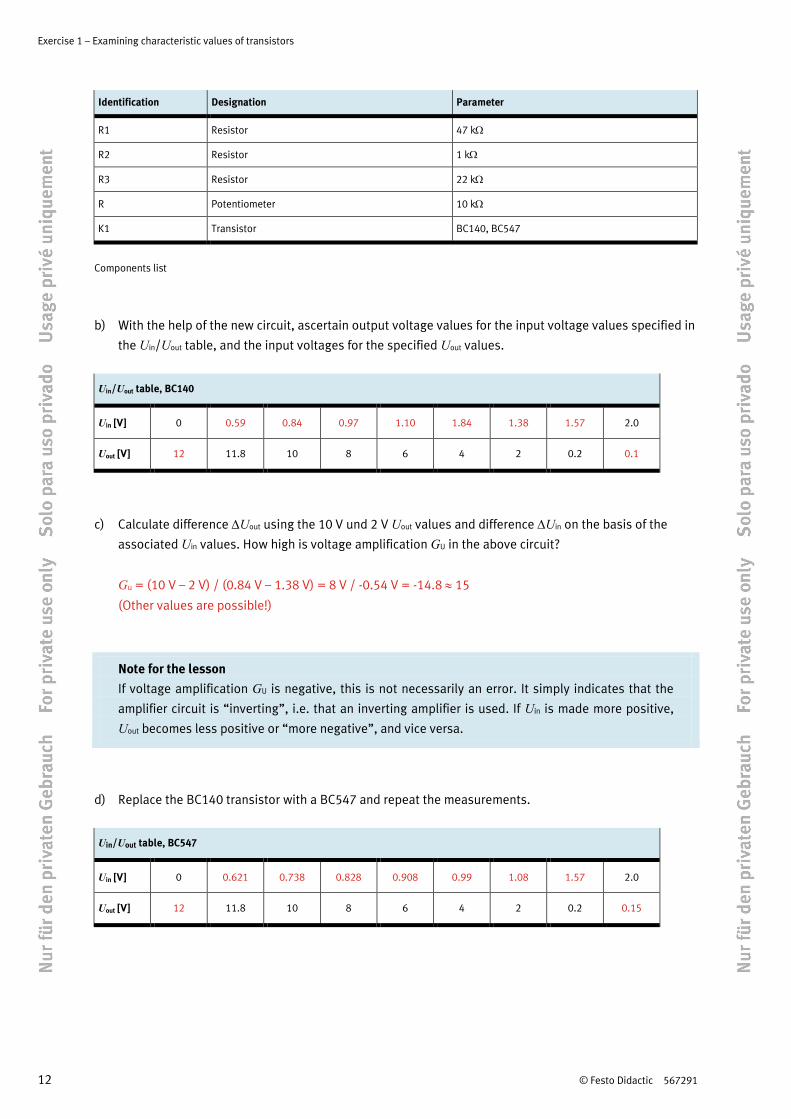
b) With the help of the new circuit, ascertain output voltage values for the input voltage values specified in
the Uin/Uout table, and the input voltages for the specified Uout values.
Uin/Uout table, BC140
Uin [V] 0 0.59 0.84 0.97 1.10 1.84 1.38 1.57 2.0
Uout [V] 12 11.8 10 8 6 4 2 0.2 0.1
c) Calculate difference ∆Uout using the 10 V und 2 V Uout values and difference ∆Uin on the basis of the
associated Uin values. How high is voltage amplification GU in the above circuit?
Gu = (10 V – 2 V) / (0.84 V – 1.38 V) = 8 V / -0.54 V = -14.8 ≈ 15
(Other values are possible!)
Note for the lesson If voltage amplification GU is negative, this is not necessarily an error. It simply indicates that the
amplifier circuit is “inverting”, i.e. that an inverting amplifier is used. If Uin is made more positive,
Uout becomes less positive or “more negative”, and vice versa.
d) Replace the BC140 transistor with a BC547 and repeat the measurements.
Uin/Uout table, BC547
Uin [V] 0 0.621 0.738 0.828 0.908 0.99 1.08 1.57 2.0
Uout [V] 12 11.8 10 8 6 4 2 0.2 0.15
Exercise 1 – Examining characteristic values of transistors
© Festo Didactic 567291 13
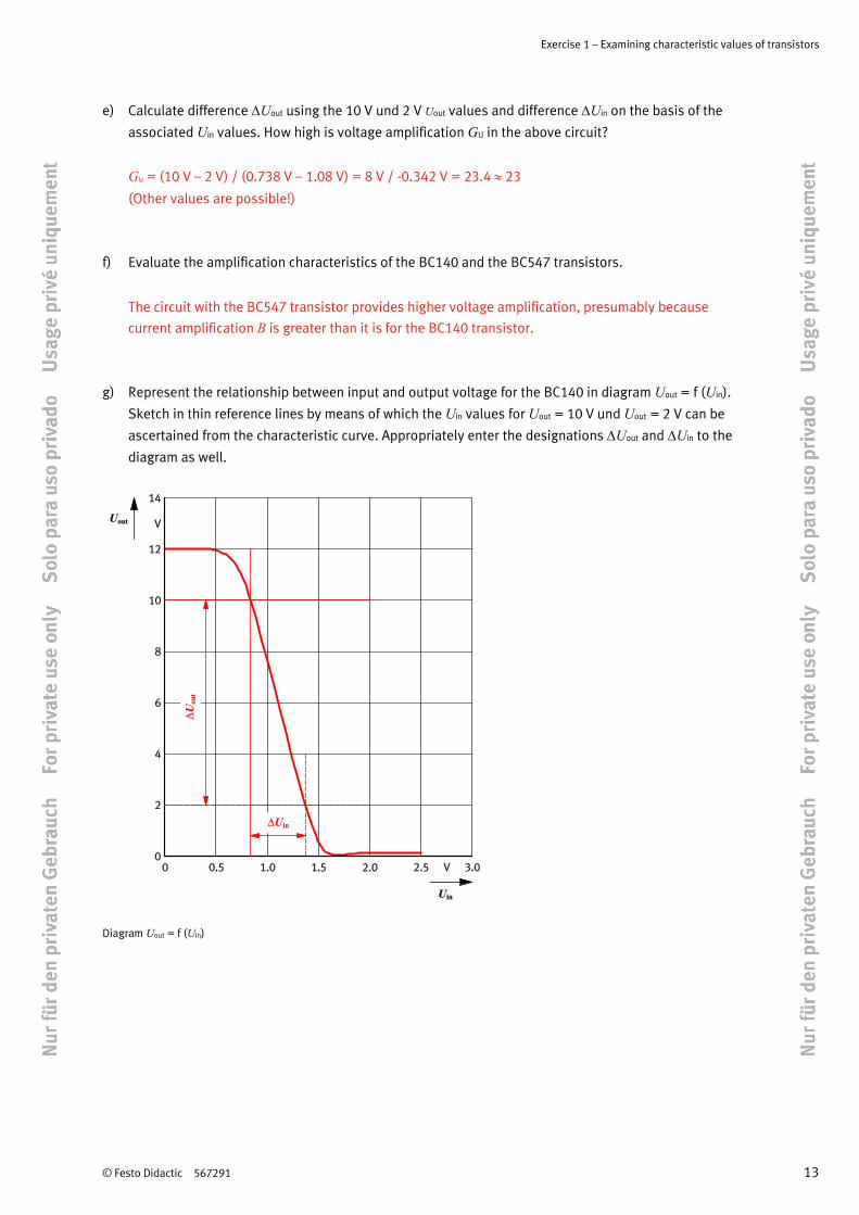
e) Calculate difference ∆Uout using the 10 V und 2 V Uout values and difference ∆Uin on the basis of the
associated Uin values. How high is voltage amplification GU in the above circuit?
Gu = (10 V – 2 V) / (0.738 V – 1.08 V) = 8 V / -0.342 V = 23.4 ≈ 23
(Other values are possible!)
f) Evaluate the amplification characteristics of the BC140 and the BC547 transistors.
The circuit with the BC547 transistor provides higher voltage amplification, presumably because
current amplification B is greater than it is for the BC140 transistor.
g) Represent the relationship between input and output voltage for the BC140 in diagram Uout = f (Uin).
Sketch in thin reference lines by means of which the Uin values for Uout = 10 V und Uout = 2 V can be
ascertained from the characteristic curve. Appropriately enter the designations ∆Uout and ∆Uin to the
diagram as well.
Diagram Uout = f (Uin)
Exercise 1 – Examining characteristic values of transistors
14 © Festo Didactic 567291
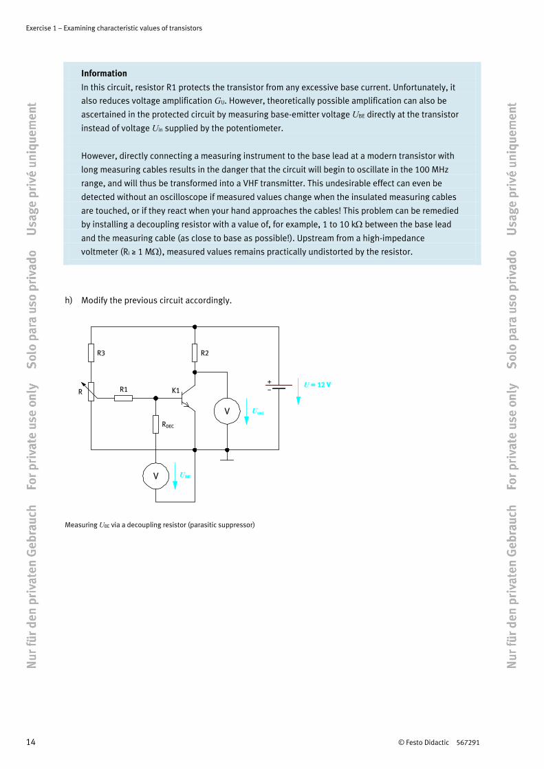
Information
In this circuit, resistor R1 protects the transistor from any excessive base current. Unfortunately, it
also reduces voltage amplification GU. However, theoretically possible amplification can also be
ascertained in the protected circuit by measuring base-emitter voltage UBE directly at the transistor
instead of voltage Uin supplied by the potentiometer.
However, directly connecting a measuring instrument to the base lead at a modern transistor with
long measuring cables results in the danger that the circuit will begin to oscillate in the 100 MHz
range, and will thus be transformed into a VHF transmitter. This undesirable effect can even be
detected without an oscilloscope if measured values change when the insulated measuring cables
are touched, or if they react when your hand approaches the cables! This problem can be remedied
by installing a decoupling resistor with a value of, for example, 1 to 10 kΩ between the base lead
and the measuring cable (as close to base as possible!). Upstream from a high-impedance
voltmeter (Ri ≥ 1 MΩ), measured values remains practically undistorted by the resistor.
h) Modify the previous circuit accordingly.
Measuring UBE via a decoupling resistor (parasitic suppressor)
Exercise 1 – Examining characteristic values of transistors
© Festo Didactic 567291 15
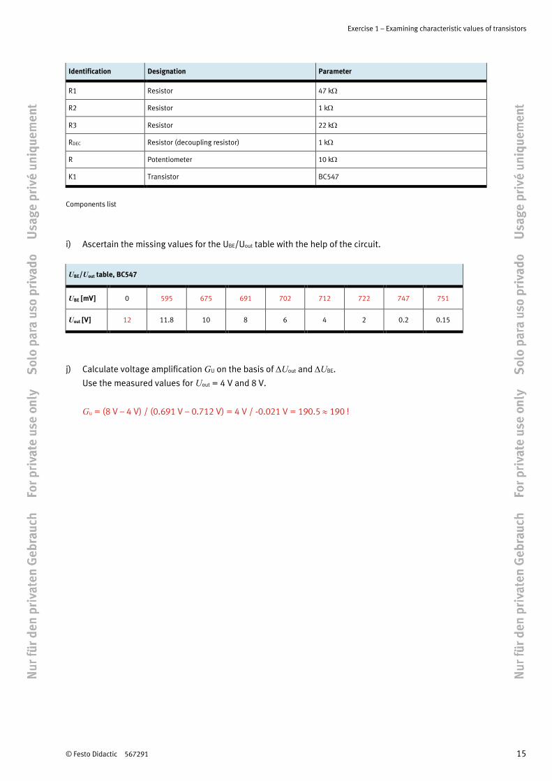
Identification Designation Parameter
R1 Resistor 47 kΩ
R2 Resistor 1 kΩ
R3 Resistor 22 kΩ
RDEC Resistor (decoupling resistor) 1 kΩ
R Potentiometer 10 kΩ
K1 Transistor BC547
Components list
i) Ascertain the missing values for the UBE/Uout table with the help of the circuit.
UBE/Uout table, BC547
UBE [mV] 0 595 675 691 702 712 722 747 751
Uout [V] 12 11.8 10 8 6 4 2 0.2 0.15
j) Calculate voltage amplification GU on the basis of ∆Uout and ∆UBE.
Use the measured values for Uout = 4 V and 8 V.
Gu = (8 V – 4 V) / (0.691 V – 0.712 V) = 4 V / -0.021 V = 190.5 ≈ 190 !
Exercise 1 – Examining characteristic values of transistors
16 © Festo Didactic 567291
6. The transistor as alternating voltage amplifier
Information
Input voltage, which has thus far been adjusted manually with potentiometer R, can also be
changed by injecting an alternating voltage. In order to assure that direct current flowing through
R1 is not inadvertently drained off via the alternating voltage source, a so-called “coupling
capacitor” (C1) is installed into the signal line. It has infinitely high resistance XC for direct current,
but allows alternating current to pass freely. Potentiometer R can now be used to set the amplifier’s
operating point.
Due to the fact that small alternating voltages alone are not capable of rendering a transistor
conductive, the transistor is influenced with a direct current such that collector voltage UC is about
halfway between its two extreme values, UEmax and UEmin, in the idle state. If a (small) alternating
current is now added to direct base current, the direct current is then increased and reduced
synchronous to the alternating signal cycles (undulating current occurs). Correspondingly, collector
current IC and collector voltage UC oscillate around their quiescent values synchronous to the input
signal.
The alternating voltage component is filtered back out of the undulating collector voltage with
additional coupling capacitor C2, which is then used as output signal Uout. In this way, the amplifier
circuit creates a considerably larger (amplified) alternating voltage signal at the output from a small
one at the input (with identical frequency and waveform) – even though, in this case, the transistor
works with positive operating voltage U only!
After measuring peak-to-peak values for the input and output signals with a oscilloscope, these
values can be used to calculate the circuit’s alternating voltage amplification GU(AC).
Alternating voltage amplification gain out(ss) out(eff)U(AC)
in(ss) in(eff)
U UG
U U= =

Exercise 1 – Examining characteristic values of transistors
© Festo Didactic 567291 17
The transistor as an alternating voltage amplifier
Y1: to oscilloscope, channel A
Y2: to oscilloscope, channel B
Identification Designation Parameter
R1 Resistor 100 kΩ
R2 Resistor 1 kΩ
R3 Resistor 10 kΩ
R Potentiometer 10 kΩ
C1 Capacitor 220 µF
C2 Electrolytic capacitor 10 µF
K1 Transistor BC140
Components list
Notes
In order to be able to observe the operations which take place within the circuit in a relaxed
fashion:
– Set the EduTrainer sine-wave generator to a very low frequency, for
example 0.2 Hz.
– Roughly 0.1 to 0.3 V suffice for Uin (take from the 0 to 2 V output of the DDS
waveform generator!).
– Adjust the oscilloscope such that both channels record two steady, uninterrupted
lines, which move up and down synchronous to the input signal.
– Disconnect the sine-wave generator from C1 and set the circuit’s operating point to
UCE = +6 V (50% of operating voltage) with the potentiometer.
– Reconnect the generator and adjust the amplitude of Uin such that
transistor voltage UCE oscillates between roughly +4 and +8 V.
Exercise 1 – Examining characteristic values of transistors
18 © Festo Didactic 567291
a) Experiment with the circuit and then answer the following questions. Tick the correct answers.
Input voltage Uin(AC) and output voltage Uout(AC) oscillate synchronously.
Input voltage Uin(AC) and output voltage Uout(AC) oscillate oppositely.
During the positive half-wave of Uin(AC), more collector current IC flows than during the negative half-
wave of Uin(AC).
During the positive half-wave of Uin(AC), less collector current IC flows than during the negative half-wave
of Uin(AC).
When collector current in the transistor increases, collector-emitter voltage UCE rises as well.
When collector current in the transistor increases, collector-emitter voltage UCE drops.
An operating point UC amounting to 50% of operating voltage is selected because from there, collector
voltage can move up or down by the same amount.
An operating point UC amounting to 50% of operating voltage is selected because this is where
amplification within the circuit is greatest.
Coupling capacitors are intended to allow alternating signals to pass, but should not influence direct
voltage.
Coupling capacitors prevent unwanted high frequency oscillation within the circuit.
The operating point is the basic setting for direct current within a circuit.
The operating point is a the solder joint in the circuit diagram which connects the collector to the
output.
Exercise 1 – Examining characteristic values of transistors
© Festo Didactic 567291 19
7. Relationship between operating point setting and output signal distortion
Information
The circuit is usually tested with signals which result in a stationary pattern at the oscilloscope.
Increase the frequency of the input signal to 500 Hz to this end, and set the sweep at the
oscilloscope such that one to two full periods for Uin(AC) and Uout(AC) can be viewed at the screen.
a) Adjust the input signal and the operating point such that a clean sinusoidal signal with 6 V peak-to-peak
(6 Vpp) is generated at the output. Then measure the peak-to-peak value for Uin(AC) and ascertain
alternating voltage amplification GU(AC) for the circuit.
Where Uout = 6 Vpp, the amplifier requires an input voltage of Uin = 250 mVpp.
The following results: Gu = 6 Vpp / 0.25 Vpp = 24
b) How many degrees does phase shifting amount to between Uin(AC) and Uout(AC)?
Uout is displaced from Uin by one half-wave (180°). The negative half-wave of von Uout occurs during the
positive half-wave of Uin, and vice versa.
c) What happens to the waveform of the output signal if the operating point is slowly adjusted up or down
with potentiometer R?
The positive or negative peaks of the alternating output voltage are chopped.
The sinusoidal waveform is distorted.
d) Find the answer to the following question by changing Uin(AC) and the operating point:
How much peak-to-peak voltage voltage can be delivered at the output without distorting the sinusoidal
waveform?
Distortion is relatively minimal for output voltage of up to about 10 Vpp.
Exercise 1 – Examining characteristic values of transistors
20 © Festo Didactic 567291
Information
The waveform of the output signal of a hi-fi amplifier must be identical to that of its input signal.
However, signal inverting is not taken into consideration. If one channel can be inverted and Y
deflection can be infinitely adjusted at your oscilloscope, you can attempt to bring the Uout(AC) and
Uin(AC) signals into coincidence at the screen. The closer you come to succeeding, the better the
amplifier is.
e) Test response characteristics with delta und square-wave voltage as well. Then evaluate whether or not
the amplifier is suitable for hi-fi applications, at least under certain conditions.
With peak-to-peak output signals of just a few volts, the waveforms closely approximate each other,
i.e. no visible distortion occurs. Deviation becomes greater as amplitude is increased. For this reason,
the amplifier is only suitable for hi-fi applications under certain conditions.
8. Basic transistor circuits
Information
There are three basic transistor circuits. They are named after the transistor lead which serves as a
common point of reference for the input and output signals. In the simplest of all cases, this is the
transistor lead which is connected to ground. But there is frequently no direct connection from
there to circuit grounding. In this case, the following method is helpful in determining the correct
name: Find out to which transistor lead the input signal is applied, and from which lead the output
signal is taken. The basic circuit is named after the remaining transistor lead.
a) Which type of basic transistor circuit was used in the preceding pages? Tick the correct answer.
In the test and experimental circuits covered by exercise 1, the transistors were used in a common
emitter circuit, or common emitter for short.
In the test and experimental circuits covered by exercise 1, the transistors were used in a common base
circuit, or base for short.
In the test and experimental circuits covered by exercise 1, the transistors were used in a basic common
collector, or common collector for short.
© Festo Didactic 567291 1
Table of contents
Exercises and worksheets
Exercise 1: Examining characteristic values of transistors _________________________________________ 3
Exercise 2: Differentiating basic transistor circuits ______________________________________________ 21
Exercise 3: Examining multistage amplifiers ___________________________________________________ 39
Exercise 4: Setting up a power amplifier ______________________________________________________ 57
Exercise 5: Amplifying direct voltage signals___________________________________________________ 73
Exercise 6: Generating pulse voltage and sawtooth voltage ______________________________________ 91
Exercise 7: Setting up sine-wave generators with LC and RC elements ____________________________ 111
Exercise 8: Examining power pack circuits ___________________________________________________ 129
Exercise 9: Becoming familiar with DC voltage converters _______________________________________ 147
Exercise 10: Using thyristors and triacs _______________________________________________________ 163

2 © Festo Didactic 567291

© Festo Didactic 567291 3
Exercise 1 Examining characteristic values of transistors
Learning objectives
After completing this exercise:
• You will know how to test transistors for correct functioning.
• You will be able to ascertain current amplification B for transistors.
• You will be familiar with typical current amplification values for transistors.
• You will know how to convert circuits for NPN transistors into circuits for PNP transistors.
• You will be able to ascertain a circuit’s voltage amplification.
• You will be familiar with the effects of operating point adjustments.
• You will be familiar with the effects of overdriving an amplifier.
Problem description
You work for a company that manufactures and repairs hi-fi amplifiers. During the course of initial training
you will need to familiarise yourself with the performance of transistors and their typical characteristic
values.
You will set up a test circuit to this end, which allows you to determine the degree to which transistors
amplify power. After slightly modifying the circuit, you will then examine how a transistor can be used as a
voltage amplifier.

Exercise 1 – Examining characteristic values of transistors
4 Name: __________________________________ Date: ____________ © Festo Didactic 567291
Project assignments
1. Set up a test circuit with NPN transistor BC140 and ascertain the transistor’s power amplification B with
collector current values of IC = 1 mA, 5 mA and 10 mA.
2. For purposes of comparison, determine power amplification B for transistor BC547.
3. Modify the test circuit so that it is suitable for testing PNP transistors, and ascertain power amplification
B for transistor BC160.
4. Set sup a test circuit within which transistors are actuated non-destructively with direct voltage.
Familiarise yourself with the basic principle of voltage amplification.
5. With the help of the test circuit, determine voltage amplification GU when using transistors BC140 and
BC547.
6. Expand the test circuit such that a BC140 transistor can be additionally actuated with alternating
voltage. Familiarise yourself with the concept of alternating voltage amplification.
7. Examine the relationship between operating point setting and output signal distortion.
8. Find out whether the test circuit is a basic common emitter circuit, a basic fundamental circuit or a basic
common collector.
Work aids
• Textbooks, books of tables
• Excerpts from manufacturers’ catalogues
• Data sheets
• Internet
• WBT Electronics 1 and Electronics 2
Exercise 1 – Examining characteristic values of transistors
© Festo Didactic 567291 Name: __________________________________ Date: ____________ 5
Information
Basic knowledge regarding diodes and transistors
Transistors and diodes consist of semiconductor materials, for the most part silicon.
Semiconductors can be influenced by inserting dopants such that current flows within them either
through negative charge carriers (electrons) or positive charge carriers (so-called “holes” or
“defect electrons”). Semiconductors modified in this way are called n-material and p-material
respectively.
When p-material and n-material is joined, a PN transition occurs. The transition only allows
electrical current to pass in one direction, and thus functions as an electrical valve or diode. The
function of the diode can be readily explained with the basic electrical law which states that “unlike
charges attract each other and like charges repel each other”.
Semiconductor diode – circuit symbol and layout
• Blocked direction
If the n-region of the PN transition is connected to the plus pole of a voltage source and the
p-zone is connected to the minus pole, the charge carriers in the semiconductor are drawn
outward. As a result, a broad region which is free of charge carriers is created at the
PN transition which functions as an insulating layer and prevents the flow of current.
The PN transition (the diode) blocks flow.
• Free-flow direction
If the polarity of the external voltage source is reversed (plus to p-region and minus to
n-region), the charge carriers are driven towards each other in both regions and (after
exceeding a given “threshold voltage”) are capable of passing through the PN transition.
Current flows. The diode is conductive.
• The diode terminal which is connected to the n-region is called the cathode, and the terminal
connected to the p-region is called the anode.
• The arrow in the circuit symbol indicates the free-flow direction for the
flow of current.
Exercise 1 – Examining characteristic values of transistors
6 Name: __________________________________ Date: ____________ © Festo Didactic 567291
Transistors (more precisely “bipolar transistors”) consist of three semiconductor layers in one of
the following orders: N-P-N or P-N-P. The middle layer is the base layer, and the two outside layers
are known as the emitter and collector layers. This is why transistor terminals are usually
designated with the abbreviations E, B and C.
NPN and PNP transistors – layout and circuit symbol
The polarity of a transistor’s operating voltage must always be set up such that the charge carriers
from the emitter region are drawn to the collector. Due to the fact that unlike charges are attracted
to each other, the following results:
• NPN transistors work with positive collector-emitter voltage UCE
• PNP transistors work with negative collector-emitter voltage UCE
However, without base voltage no flow of charge carriers takes place from the emitter to the
collector. The base layer prevents the collector’s attractive force from extending into the emitter
region. Only after charge carriers are lifted out of the emitter region into the (thin) base layer with
the help of base voltage are they subjected to the influence of the collector’s attraction region, to
which most of them then flow. In order to draw the charge carriers from the emitter to the base,
base-emitter voltage UBE must have the same polarity as collector-emitter voltage UCE. This results
in the following:
• NPN transistors become conductive in the case of positive base-emitter voltage UBE.
• PNP transistors become conductive in the case of negative base-emitter voltage UBE.
And thus the basic function of the transistor as an amplifier component can be explained as follows:
With the help of relatively minimal base-emitter voltage UBE, we can control how many charge
carriers flow from the transistor’s emitter to its collector. However, base current IB can also be
specified in order to control collector current. Each specific base current value automatically results
in a certain base-emitter voltage UBE, which in turn dictates a given collector current IC.
Nevertheless, the relationship between collector current IC and base current IB is far more linear
than the relationship between IC and UBE. Ratio IC / IB is know as transistor current amplification B.
The ratio may vary from one transistor to the next, and usually lies within a range of 50 to 500.

Exercise 1 – Examining characteristic values of transistors
© Festo Didactic 567291 Name: __________________________________ Date: ____________ 7
The equivalent circuit diagram of a transistor demonstrates its mode of operation in an even
simpler fashion: The transistor’s base-emitter path functions like a diode in the free-flow direction.
Base current IB flowing along this path increases current IC between emitter and collector by a factor
of B. The current source symbol indicates that collector current is for the most part independent of
the collector voltage value.
NPN transistor – equivalent circuit diagram
The emitter is identified with an arrow in the transistor symbol. Regardless of internal processes
within the transistor, the direction of the arrow in the symbol nevertheless represents the actual
direction of flow. The following applies in general to symbols for semiconductor components: The
arrow points either towards a p-region or comes out of an n-region. (mnemonic aid: P = “pointing”
arrow, N = “advancing” arrow).
What does an amplifier do?
The microphone in a telephone converts sound waves created by, for example, speech or music,
into alternating voltage in the millivolt range. However, this signal is too weak to drive a headphone
or a loudspeaker directly. Several volts are required for good, audible reproduction with these
devices. An amplifier must therefore be connected between the microphone and the headphone or
loudspeaker. All amplifiers require (direct) operating voltage in order to generate an output signal.
Amplifier – circuit symbol
In the following pages you will learn how transistor amplifiers work.
Exercise 1 – Examining characteristic values of transistors
8 Name: __________________________________ Date: ____________ © Festo Didactic 567291
1. Current amplification with NPN transistor BC140
Information
The transistor as a current amplifier
You can test NPN transistors for correct functioning with the following circuit. Transistor base
current IB can be adjusted with the variable voltage divider (potentiometer). Assuming that the
transistor is intact, any base current causes significantly increased collector current IC. By dividing
the measured value for IC by the measured value for IB, we arrive at current amplification gain B for
the transistor under test.
C
B
IBI
=
Resistors R1 and R2 are so-called protective resistors. They limit base and collector current to
values which are incapable of damaging the transistor, in the event that potentiometer R is
operated without due care.
Test circuit for measuring current amplification B
Identification Designation Parameter
R1 Resistor 10 kΩ, 47 kΩ, 100 kΩ (depending on task)
R2 Resistor 1 kΩ
R Potentiometer 10 kΩ
K1 Transistor BC140, BC547, BC160 (depending on task)
Components list
Exercise 1 – Examining characteristic values of transistors
© Festo Didactic 567291 Name: __________________________________ Date: ____________ 9
a) Set up the test circuit with a BC140 transistor and set IC to a value of 1 mA. Read base current IB and
make a note of its value. Calculate current amplification B for the transistor under test on the basis of
the measured values. Repeat measurement after setting IC to a value of 5 mA and 10 mA. Enter the
obtained values to the table under BC140 (1).
Transistor BC140 (1) BC140 (2) BC547 BC160
IC [mA] 1 5 10 1 5 10 1 5 10 1 5 10
IB [µA]
B = IC / IB
Table of measured values
b) A second BC140 transistor is included in the set of components furnished with the EduTrainer. Test it in
the same way and ascertain current amplification B where IC = 1 mA, 5 mA and 10 mA. Enter the values
to the table under BC140 (2).
(It is entirely normal for current amplification gain to vary from on transistor to the next, even for
transistors of the same type!)
2. Current amplification with NPN transistor BC547
a) Repeat the procedure with transistor BC547 and enter the values to the table.
3. Current amplification with PNP transistor BC160
a) Transistor BC160 is a PNP transistor. The measuring circuit used thus far must be slightly modified in
order to assure that the transistor functions correctly. What needs to be done?
b) Using the modified test circuit, ascertain the missing data for the BC160 transistor and enter them to
the table.
Exercise 1 – Examining characteristic values of transistors
10 Name: __________________________________ Date: ____________ © Festo Didactic 567291
c) Leave the transistor in the circuit in order to conduct research experiments.
1. What is the highest base current which can be selected with the potentiometer?
2. Try to calculate this value using data obtained with the test circuit.
3. What is the largest collector current value which can be set up with the circuit?
4. Try to calculate ICmax using the data obtained with the test circuit.
5. Up to limit value ICmax, collector current IC can be controlled by adjusting
base current IB. What is the designation for the transistor’s state when it no longer responds to
further control signal increases?
6. What has to be done in order to expand the test circuit for collector current of up to roughly 25 mA?
Exercise 1 – Examining characteristic values of transistors
© Festo Didactic 567291 Name: __________________________________ Date: ____________ 11
4. The transistor as a voltage amplifier
Information
With the help of (direct) operating voltage (designated U in this workbook), transistors can also be
used as voltage amplifiers. However, they have to be combined with other components to this end,
which convert current changes to voltage changes. In the simplest of all cases, “operating
resistance RA” is connected to the collector lead. The transistor and the resistor comprise a series
connection through which collector current IC flows. In accordance with Ohm’s law, voltage drop
over working resistance results from the equation URA = RA ⋅ IC, and voltage drop UCE results from
the laws of series connection: UCE = UC = U – URA. In this way, input voltage Uin first of all controls
base current IB, and thus collector current IC as well, and finally collector voltage UC too, thanks to
operating resistance RA. Collector voltage then serves as output voltage Uout. With regard to a
circuit’s voltage amplification GU we do not consider direct voltage at the input and the output,
rather man the ratio of “voltage change at the output” to the “causative voltage change at the
input. “Change” or difference is represented in formulas with the Greek letter ∆ (delta). And thus
the following notation results:
Voltage amplification out1 out2 outU
in1 in2 in
U U UG
U U U− ∆
= =− ∆
5. Voltage amplification with NPN transistors BC140 and BC547
a) Convert the previously used test circuit into a voltage amplifier.
The transistor as a voltage amplifier
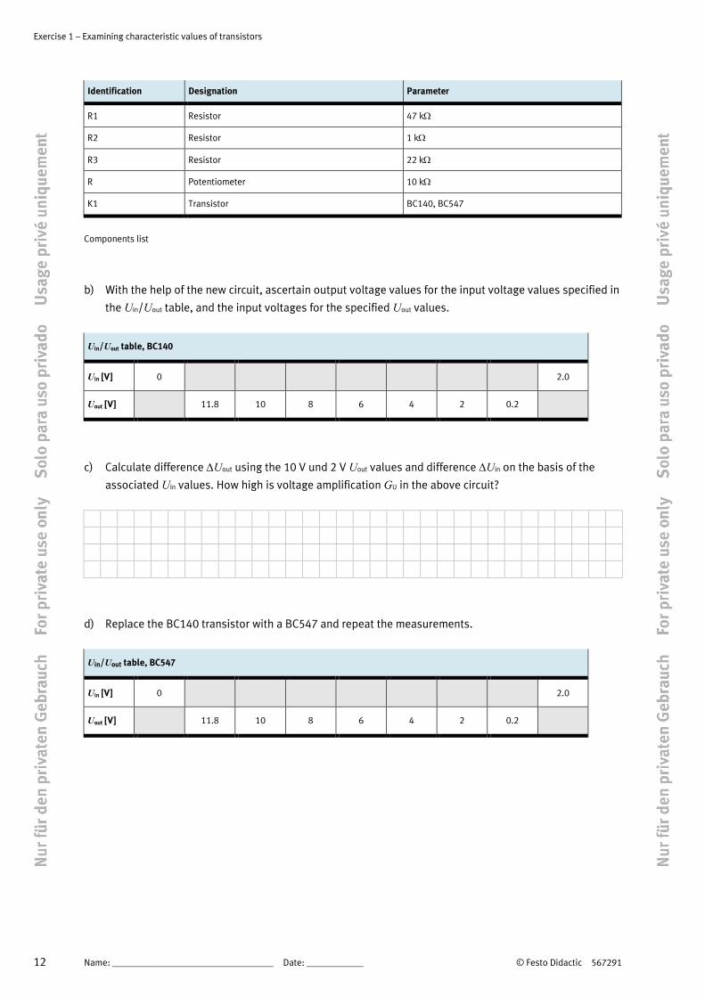
Exercise 1 – Examining characteristic values of transistors
12 Name: __________________________________ Date: ____________ © Festo Didactic 567291
Identification Designation Parameter
R1 Resistor 47 kΩ
R2 Resistor 1 kΩ
R3 Resistor 22 kΩ
R Potentiometer 10 kΩ
K1 Transistor BC140, BC547
Components list
b) With the help of the new circuit, ascertain output voltage values for the input voltage values specified in
the Uin/Uout table, and the input voltages for the specified Uout values.
Uin/Uout table, BC140
Uin [V] 0 2.0
Uout [V] 11.8 10 8 6 4 2 0.2
c) Calculate difference ∆Uout using the 10 V und 2 V Uout values and difference ∆Uin on the basis of the
associated Uin values. How high is voltage amplification GU in the above circuit?
d) Replace the BC140 transistor with a BC547 and repeat the measurements.
Uin/Uout table, BC547
Uin [V] 0 2.0
Uout [V] 11.8 10 8 6 4 2 0.2
Exercise 1 – Examining characteristic values of transistors
© Festo Didactic 567291 Name: __________________________________ Date: ____________ 13
e) Calculate difference ∆Uout using the 10 V und 2 V Uout values and difference ∆Uin on the basis of the
associated Uin values. How high is voltage amplification GU in the above circuit?
f) Evaluate the amplification characteristics of the BC140 and the BC547 transistors.
g) Represent the relationship between input and output voltage for the BC140 in diagram Uout = f (Uin).
Sketch in thin reference lines by means of which the Uin values for Uout = 10 V und Uout = 2 V can be
ascertained from the characteristic curve. Appropriately enter the designations ∆Uout and ∆Uin to the
diagram as well.
Uout
0 0.5 1.0 1.5 2.0 2.5 3.00
2
4
6
8
10
12
14
Uin
V
V
Diagram Uout = f (Uin)
Exercise 1 – Examining characteristic values of transistors
14 Name: __________________________________ Date: ____________ © Festo Didactic 567291
Information
In this circuit, resistor R1 protects the transistor from any excessive base current. Unfortunately, it
also reduces voltage amplification GU. However, theoretically possible amplification can also be
ascertained in the protected circuit by measuring base-emitter voltage UBE directly at the transistor
instead of voltage Uin supplied by the potentiometer.
However, directly connecting a measuring instrument to the base lead at a modern transistor with
long measuring cables results in the danger that the circuit will begin to oscillate in the 100 MHz
range, and will thus be transformed into a VHF transmitter. This undesirable effect can even be
detected without an oscilloscope if measured values change when the insulated measuring cables
are touched, or if they react when your hand approaches the cables! This problem can be remedied
by installing a decoupling resistor with a value of, for example, 1 to 10 kΩ between the base lead
and the measuring cable (as close to base as possible!). Upstream from a high-impedance
voltmeter (Ri ≥ 1 MΩ), measured values remains practically undistorted by the resistor.
h) Modify the previous circuit accordingly.
Measuring UBE via a decoupling resistor (parasitic suppressor)
Exercise 1 – Examining characteristic values of transistors
© Festo Didactic 567291 Name: __________________________________ Date: ____________ 15
Identification Designation Parameter
R1 Resistor 47 kΩ
R2 Resistor 1 kΩ
R3 Resistor 22 kΩ
RDEC Resistor (decoupling resistor) 1 kΩ
R Potentiometer 10 kΩ
K1 Transistor BC547
Components list
i) Ascertain the missing values for the UBE/Uout table with the help of the circuit.
UBE/Uout table, BC547
UBE [mV] 0
Uout [V] 11.8 10 8 6 4 2 0.2 0.15
j) Calculate voltage amplification GU on the basis of ∆Uout and ∆UBE.
Use the measured values for Uout = 4 V and 8 V.
Exercise 1 – Examining characteristic values of transistors
16 Name: __________________________________ Date: ____________ © Festo Didactic 567291
6. The transistor as alternating voltage amplifier
Information
Input voltage, which has thus far been adjusted manually with potentiometer R, can also be
changed by injecting an alternating voltage. In order to assure that direct current flowing through
R1 is not inadvertently drained off via the alternating voltage source, a so-called “coupling
capacitor” (C1) is installed into the signal line. It has infinitely high resistance XC for direct current,
but allows alternating current to pass freely. Potentiometer R can now be used to set the amplifier’s
operating point.
Due to the fact that small alternating voltages alone are not capable of rendering a transistor
conductive, the transistor is influenced with a direct current such that collector voltage UC is about
halfway between its two extreme values, UEmax and UEmin, in the idle state. If a (small) alternating
current is now added to direct base current, the direct current is then increased and reduced
synchronous to the alternating signal cycles (undulating current occurs). Correspondingly, collector
current IC and collector voltage UC oscillate around their quiescent values synchronous to the input
signal.
The alternating voltage component is filtered back out of the undulating collector voltage with
additional coupling capacitor C2, which is then used as output signal Uout. In this way, the amplifier
circuit creates a considerably larger (amplified) alternating voltage signal at the output from a small
one at the input (with identical frequency and waveform) – even though, in this case, the transistor
works with positive operating voltage U only!
After measuring peak-to-peak values for the input and output signals with a oscilloscope, these
values can be used to calculate the circuit’s alternating voltage amplification GU(AC).
Alternating voltage amplification gain out(ss) out(eff)U(AC)
in(ss) in(eff)
U UG
U U= =
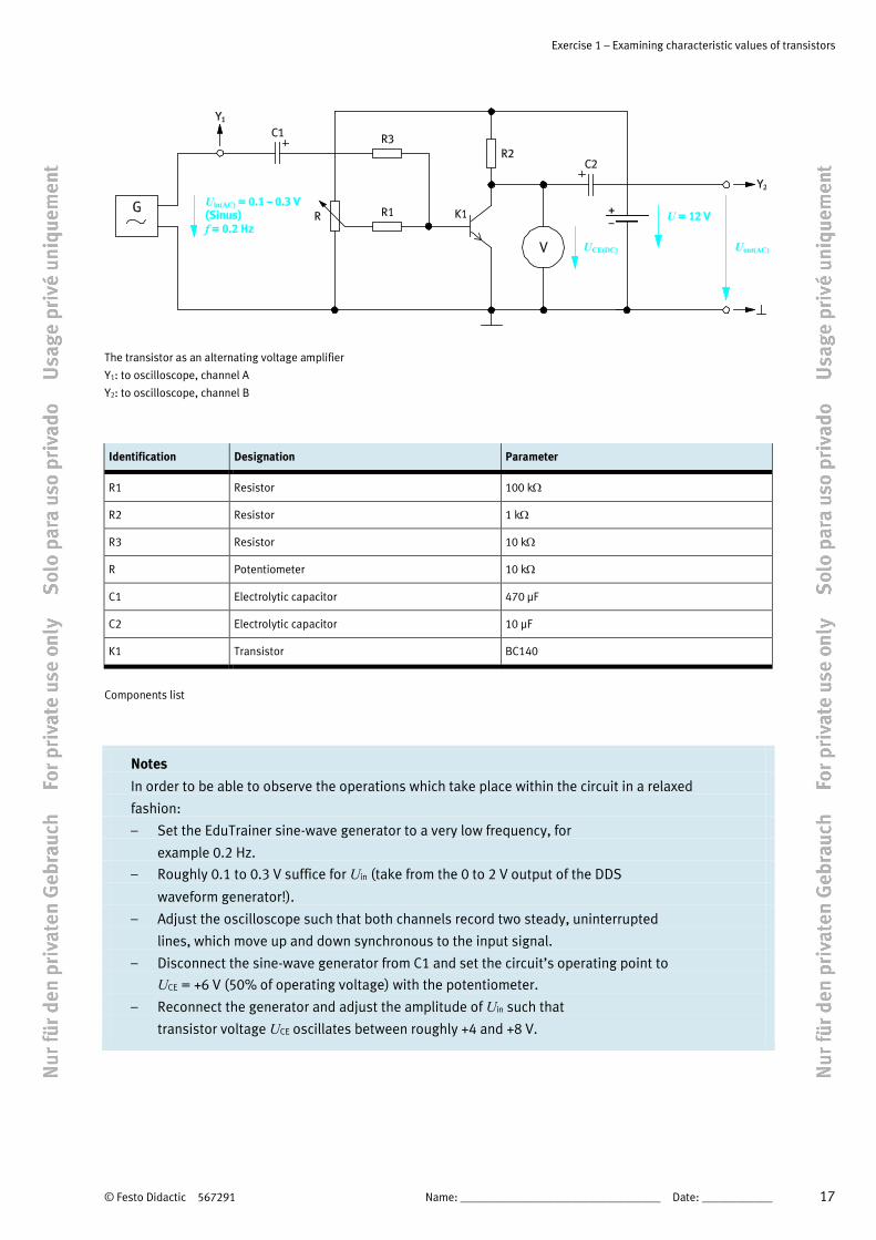
Exercise 1 – Examining characteristic values of transistors
© Festo Didactic 567291 Name: __________________________________ Date: ____________ 17
The transistor as an alternating voltage amplifier
Y1: to oscilloscope, channel A
Y2: to oscilloscope, channel B
Identification Designation Parameter
R1 Resistor 100 kΩ
R2 Resistor 1 kΩ
R3 Resistor 10 kΩ
R Potentiometer 10 kΩ
C1 Electrolytic capacitor 470 µF
C2 Electrolytic capacitor 10 µF
K1 Transistor BC140
Components list
Notes
In order to be able to observe the operations which take place within the circuit in a relaxed
fashion:
– Set the EduTrainer sine-wave generator to a very low frequency, for
example 0.2 Hz.
– Roughly 0.1 to 0.3 V suffice for Uin (take from the 0 to 2 V output of the DDS
waveform generator!).
– Adjust the oscilloscope such that both channels record two steady, uninterrupted
lines, which move up and down synchronous to the input signal.
– Disconnect the sine-wave generator from C1 and set the circuit’s operating point to
UCE = +6 V (50% of operating voltage) with the potentiometer.
– Reconnect the generator and adjust the amplitude of Uin such that
transistor voltage UCE oscillates between roughly +4 and +8 V.
Exercise 1 – Examining characteristic values of transistors
18 Name: __________________________________ Date: ____________ © Festo Didactic 567291
a) Experiment with the circuit and then answer the following questions. Tick the correct answers.
Input voltage Uin(AC) and output voltage Uout(AC) oscillate synchronously.
Input voltage Uin(AC) and output voltage Uout(AC) oscillate oppositely.
During the positive half-wave of Uin(AC), more collector current IC flows than during the negative half-
wave of Uin(AC).
During the positive half-wave of Uin(AC), less collector current IC flows than during the negative half-wave
of Uin(AC).
When collector current in the transistor increases, collector-emitter voltage UCE rises as well.
When collector current in the transistor increases, collector-emitter voltage UCE drops.
An operating point UC amounting to 50% of operating voltage is selected because from there, collector
voltage can move up or down by the same amount.
An operating point UC amounting to 50% of operating voltage is selected because this is where
amplification within the circuit is greatest.
Coupling capacitors are intended to allow alternating signals to pass, but should not influence direct
voltage.
Coupling capacitors prevent unwanted high frequency oscillation within the circuit.
The operating point is the basic setting for direct current within a circuit.
The operating point is a the solder joint in the circuit diagram which connects the collector to the
output.
Exercise 1 – Examining characteristic values of transistors
© Festo Didactic 567291 Name: __________________________________ Date: ____________ 19
7. Relationship between operating point setting and output signal distortion
Information
The circuit is usually tested with signals which result in a stationary pattern at the oscilloscope.
Increase the frequency of the input signal to 500 Hz to this end, and set the sweep at the
oscilloscope such that one to two full periods for Uin(AC) and Uout(AC) can be viewed at the screen.
a) Adjust the input signal and the operating point such that a clean sinusoidal signal with 6 V peak-to-peak
(6 Vpp) is generated at the output. Then measure the peak-to-peak value for Uin(AC) and ascertain
alternating voltage amplification GU(AC) for the circuit.
b) How many degrees does phase shifting amount to between Uin(AC) and Uout(AC)?
c) What happens to the waveform of the output signal if the operating point is slowly adjusted up or down
with potentiometer R?
d) Find the answer to the following question by changing Uin(AC) and the operating point:
How much peak-to-peak voltage voltage can be delivered at the output without distorting the sinusoidal
waveform?
Exercise 1 – Examining characteristic values of transistors
20 Name: __________________________________ Date: ____________ © Festo Didactic 567291
Information
The waveform of the output signal of a hi-fi amplifier must be identical to that of its input signal.
However, signal inverting is not taken into consideration. If one channel can be inverted and Y
deflection can be infinitely adjusted at your oscilloscope, you can attempt to bring the Uout(AC) and
Uin(AC) signals into coincidence at the screen. The closer you come to succeeding, the better the
amplifier is.
e) Test response characteristics with delta und square-wave voltage as well. Then evaluate whether or not
the amplifier is suitable for hi-fi applications, at least under certain conditions.
8. Basic transistor circuits
Information
There are three basic transistor circuits. They are named after the transistor lead which serves as a
common point of reference for the input and output signals. In the simplest of all cases, this is the
transistor lead which is connected to ground. But there is frequently no direct connection from
there to circuit grounding. In this case, the following method is helpful in determining the correct
name: Find out to which transistor lead the input signal is applied, and from which lead the output
signal is taken. The basic circuit is named after the remaining transistor lead.
a) Which type of basic transistor circuit was used in the preceding pages? Tick the correct answer.
In the test and experimental circuits covered by exercise 1, the transistors were used in a common
emitter circuit, or common emitter for short.
In the test and experimental circuits covered by exercise 1, the transistors were used in a common base
circuit, or base for short.
In the test and experimental circuits covered by exercise 1, the transistors were used in a basic common
collector, or common collector for short.


