1.1 ARM Development Board sound subsystem specification............................... 41.2 Brief Introduction to the PCM audio format ..................................................... 5
2 Development Board Audio Hardware Architecture ............................................. 72.1 Audio system block diagram ........................................................................... 72.2 Functional description – PL041 PrimeCell AACI ............................................. 82.3 The AC’97 ‘AC Link’ protocol .......................................................................... 92.4 Functional description – LM4549 Audio Codec IC ......................................... 10
3 Programming the Audio Subsystem .................................................................. 113.1 Basic set-up and use of the AACI and Codec................................................ 113.2 Working with different audio sample data widths........................................... 123.3 Working with monophonic audio data ........................................................... 133.4 Programmable features of the LM4549 codec............................................... 13
4 AACI Software examples..................................................................................... 184.1 PrimeCell driver software.............................................................................. 184.2 Simple AACI example code .......................................................................... 184.3 DMA Audio example code (DMAC-equipped boards only) ............................ 194.4 Programming an audio clip into flash memory .............................................. 274.5 List of files included in the ‘Applications Note 115’ zip file ............................. 29
At the release date of this document, the following ARM development boards are equipped withan audio codec:
• Integrator/CP
• Integrator/IM-PD1
• RealView PB926EJ-S
• RealView AB926EJ-S
• RealView Emulation Baseboard (EB)
Note: Since the AB926EJ-S and PB926EJ-S boards are largely similar from a functionalperspective, they are often collectively referred to in this Applications Note and accompanyingexample code as ‘xB926EJ-S’.
All these boards have a similar audio subsystem, which allows stereo PCM audio to be recordedor played back at a variety of bit rates. They use the same National Semiconductor LM4549audio codec IC and the same ARM PrimeCell AACI (Advanced Audio Codec Interface) logic todrive the codec.
The user guides for these boards briefly describe the audio codec IC and the PrimeCell AACI(PL041). However, what may not be clear from the documentation is which parts of eachcomponent can and can not be used, how the two work together, and hence what thespecifications of the resultant audio sub-system are. The CD-ROMs supplied with the Integratorboards also contain PrimeCell driver source code, but this is quite complex, since it containscode to exercise each part of the PrimeCell; even the areas which are unused on the Integrator.Some customers have encountered difficulty in using all this information together to enable themto write software for this peripheral.
This document attempts to describe how the LM4549 audio codec IC and ARM PL041 AACIPrimeCell function together in the above development systems. Example C source code is alsoavailable which demonstrates how to make the audio system perform simple record andplayback operations, as well as control some of the features of the codec itself, such as gain andsample rate.
1.1 ARM Development Board sound subsystem specification
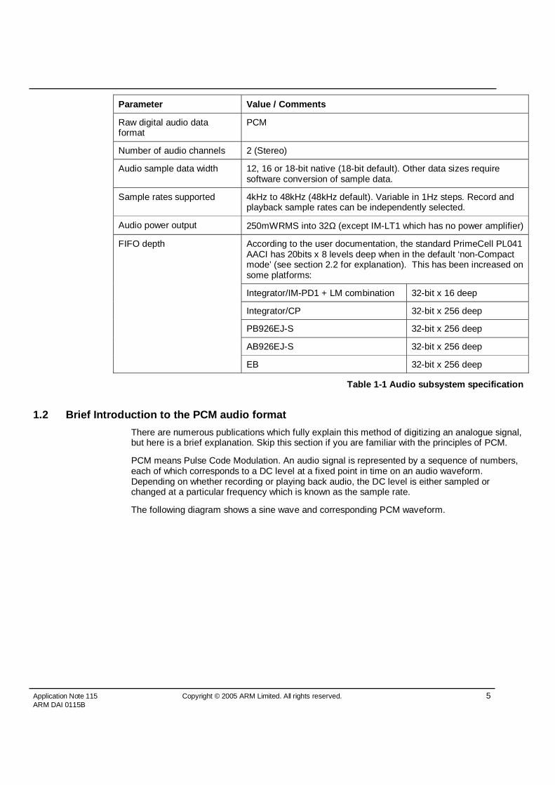
The following table lists the various audio subsystem parameters:
Audio sample data width 12, 16 or 18-bit native (18-bit default). Other data sizes requiresoftware conversion of sample data.
Sample rates supported 4kHz to 48kHz (48kHz default). Variable in 1Hz steps. Record andplayback sample rates can be independently selected.
Audio power output 250mWRMS into 32Ω (except IM-LT1 which has no power amplifier)
According to the user documentation, the standard PrimeCell PL041AACI has 20bits x 8 levels deep when in the default ‘non-Compactmode’ (see section 2.2 for explanation). This has been increased onsome platforms:
Integrator/IM-PD1 + LM combination 32-bit x 16 deep
Integrator/CP 32-bit x 256 deep
PB926EJ-S 32-bit x 256 deep
AB926EJ-S 32-bit x 256 deep
FIFO depth
EB 32-bit x 256 deep
Table 1-1 Audio subsystem specification
1.2 Brief Introduction to the PCM audio format
There are numerous publications which fully explain this method of digitizing an analogue signal,but here is a brief explanation. Skip this section if you are familiar with the principles of PCM.
PCM means Pulse Code Modulation. An audio signal is represented by a sequence of numbers,each of which corresponds to a DC level at a fixed point in time on an audio waveform.Depending on whether recording or playing back audio, the DC level is either sampled orchanged at a particular frequency which is known as the sample rate.
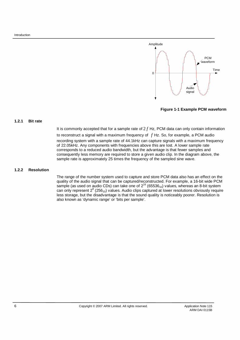
The following diagram shows a sine wave and corresponding PCM waveform.
It is commonly accepted that for a sample rate of f2 Hz, PCM data can only contain information
to reconstruct a signal with a maximum frequency of f Hz. So, for example, a PCM audiorecording system with a sample rate of 44.1kHz can capture signals with a maximum frequencyof 22.05kHz. Any components with frequencies above this are lost. A lower sample ratecorresponds to a reduced audio bandwidth, but the advantage is that fewer samples andconsequently less memory are required to store a given audio clip. In the diagram above, thesample rate is approximately 25 times the frequency of the sampled sine wave.
1.2.2 Resolution
The range of the number system used to capture and store PCM data also has an effect on thequality of the audio signal that can be captured/reconstructed. For example, a 16-bit wide PCMsample (as used on audio CDs) can take one of 216 (6553610) values, whereas an 8-bit systemcan only represent 28 (25610) values. Audio clips captured at lower resolutions obviously requireless storage, but the disadvantage is that the sound quality is noticeably poorer. Resolution isalso known as ‘dynamic range’ or ‘bits per sample’.
This section describes the audio hardware on the aforementioned development systems.
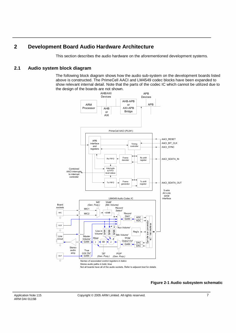
2.1 Audio system block diagram
The following block diagram shows how the audio sub-system on the development boards listedabove is constructed. The PrimeCell AACI and LM4549 codec blocks have been expanded toshow relevant internal detail. Note that the parts of the codec IC which cannot be utilized due tothe design of the boards are not shown.
ARMProcessor
AHB/AXIDevices
APBDevices
AHBor
AXI
APBAHB-APB
orAXI-APBBridge
ADCADC
DACDAC
Reg's
GAIN
GAINGAIN
'PCMOutput Vol'
'POP'(Gen. Purp.)
'MS'(Gen. Purp.)
'20dB'(Mic Volume)
'RecordSelect'
'Record Gain'
'Mic Volume'
'Line In Volume'
MIC
Board sockets
Stereoaudio amp
'MasterVolume'
5-wireAC-Link
serialinterface
Rx shift register
Tx shift register
Rx FIFO
Interrupts & FIFO
level status
Tx FIFO Frame generator
APB interface
and registers
PrimeCell AACI (PL041)
Frame decoder
Timing controller
LM4549 Audio Codec IC
AACI_RESET
AACI_BIT_CLK
AACI_SYNC
AACI_SDATA_IN
AACI_SDATA_OUT
MIC1
MIC2 +20dB
3D
CombinedAACI interrupts
to interrupt controller
Mixer
Names of associated control registers in italics
'3D'(Gen. Purp.)
Stereo audio paths in bold, blue
GAINOUT
‘True Line Out’
AUX'Aux Volume'
Linein/out
Not all boards have all of the audio sockets. Refer to adjacent text for details
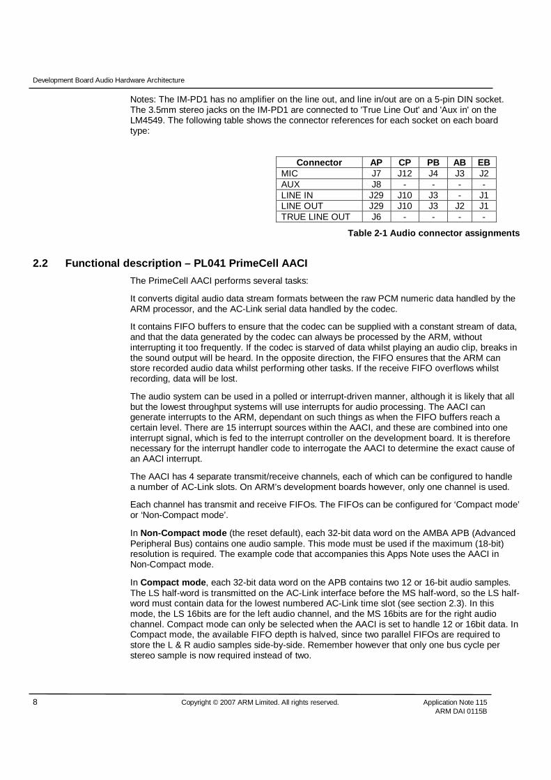
Notes: The IM-PD1 has no amplifier on the line out, and line in/out are on a 5-pin DIN socket.The 3.5mm stereo jacks on the IM-PD1 are connected to 'True Line Out' and 'Aux in' on theLM4549. The following table shows the connector references for each socket on each boardtype:
Connector AP CP PB AB EBMIC J7 J12 J4 J3 J2AUX J8 - - - -LINE IN J29 J10 J3 - J1LINE OUT J29 J10 J3 J2 J1TRUE LINE OUT J6 - - - -
Table 2-1 Audio connector assignments
2.2 Functional description – PL041 PrimeCell AACI
The PrimeCell AACI performs several tasks:
It converts digital audio data stream formats between the raw PCM numeric data handled by theARM processor, and the AC-Link serial data handled by the codec.
It contains FIFO buffers to ensure that the codec can be supplied with a constant stream of data,and that the data generated by the codec can always be processed by the ARM, withoutinterrupting it too frequently. If the codec is starved of data whilst playing an audio clip, breaks inthe sound output will be heard. In the opposite direction, the FIFO ensures that the ARM canstore recorded audio data whilst performing other tasks. If the receive FIFO overflows whilstrecording, data will be lost.
The audio system can be used in a polled or interrupt-driven manner, although it is likely that allbut the lowest throughput systems will use interrupts for audio processing. The AACI cangenerate interrupts to the ARM, dependant on such things as when the FIFO buffers reach acertain level. There are 15 interrupt sources within the AACI, and these are combined into oneinterrupt signal, which is fed to the interrupt controller on the development board. It is thereforenecessary for the interrupt handler code to interrogate the AACI to determine the exact cause ofan AACI interrupt.
The AACI has 4 separate transmit/receive channels, each of which can be configured to handlea number of AC-Link slots. On ARM’s development boards however, only one channel is used.
Each channel has transmit and receive FIFOs. The FIFOs can be configured for ‘Compact mode’or ‘Non-Compact mode’.
In Non-Compact mode (the reset default), each 32-bit data word on the AMBA APB (AdvancedPeripheral Bus) contains one audio sample. This mode must be used if the maximum (18-bit)resolution is required. The example code that accompanies this Apps Note uses the AACI inNon-Compact mode.
In Compact mode, each 32-bit data word on the APB contains two 12 or 16-bit audio samples.The LS half-word is transmitted on the AC-Link interface before the MS half-word, so the LS half-word must contain data for the lowest numbered AC-Link time slot (see section 2.3). In thismode, the LS 16bits are for the left audio channel, and the MS 16bits are for the right audiochannel. Compact mode can only be selected when the AACI is set to handle 12 or 16bit data. InCompact mode, the available FIFO depth is halved, since two parallel FIFOs are required tostore the L & R audio samples side-by-side. Remember however that only one bus cycle perstereo sample is now required instead of two.
For a full functional description, please refer to the PrimeCell PL041 Technical ReferenceManual (TRM).
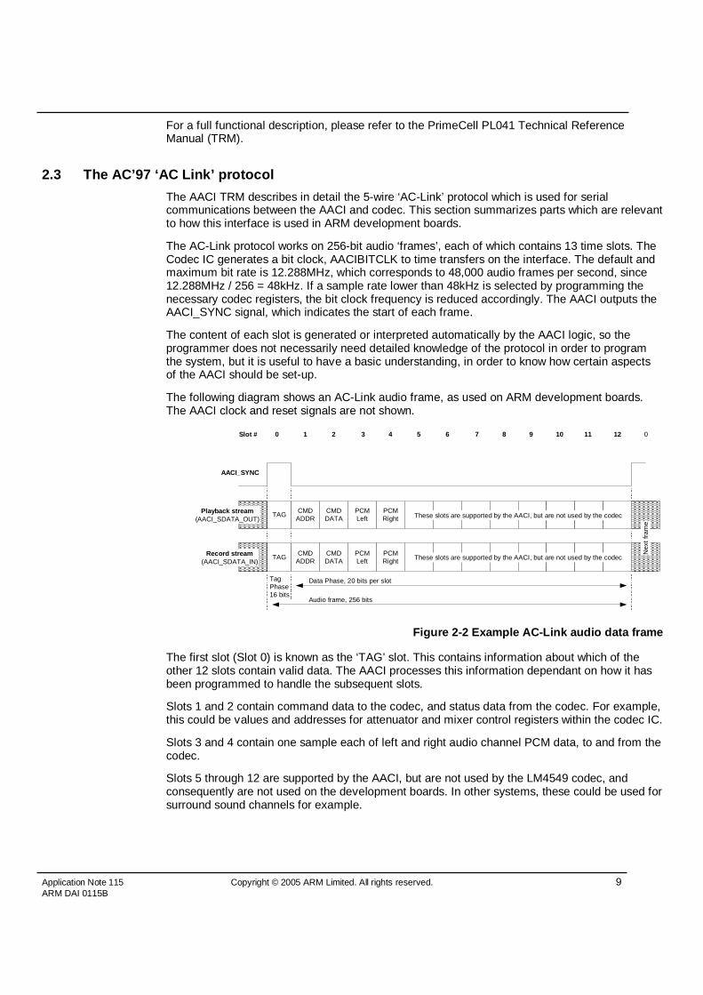
2.3 The AC’97 ‘AC Link’ protocol
The AACI TRM describes in detail the 5-wire ‘AC-Link’ protocol which is used for serialcommunications between the AACI and codec. This section summarizes parts which are relevantto how this interface is used in ARM development boards.
The AC-Link protocol works on 256-bit audio ‘frames’, each of which contains 13 time slots. TheCodec IC generates a bit clock, AACIBITCLK to time transfers on the interface. The default andmaximum bit rate is 12.288MHz, which corresponds to 48,000 audio frames per second, since12.288MHz / 256 = 48kHz. If a sample rate lower than 48kHz is selected by programming thenecessary codec registers, the bit clock frequency is reduced accordingly. The AACI outputs theAACI_SYNC signal, which indicates the start of each frame.
The content of each slot is generated or interpreted automatically by the AACI logic, so theprogrammer does not necessarily need detailed knowledge of the protocol in order to programthe system, but it is useful to have a basic understanding, in order to know how certain aspectsof the AACI should be set-up.
The following diagram shows an AC-Link audio frame, as used on ARM development boards.The AACI clock and reset signals are not shown.
AACI_SYNC
CMDADDR
CMDDATA
PCMLeft
PCMRight
0Slot # 1 2 3 4 5 6 7 8 9 10 11 12 0
Playback stream(AACI_SDATA_OUT)
CMDADDR
CMDDATA
PCMLeft
PCMRight
Record stream(AACI_SDATA_IN)
These slots are supported by the AACI, but are not used by the codec
These slots are supported by the AACI, but are not used by the codec
TagPhase16 bits
TAG
TAG
Data Phase, 20 bits per slot
Audio frame, 256 bits
Nex
tfr
ame
Figure 2-2 Example AC-Link audio data frame
The first slot (Slot 0) is known as the ‘TAG’ slot. This contains information about which of theother 12 slots contain valid data. The AACI processes this information dependant on how it hasbeen programmed to handle the subsequent slots.
Slots 1 and 2 contain command data to the codec, and status data from the codec. For example,this could be values and addresses for attenuator and mixer control registers within the codec IC.
Slots 3 and 4 contain one sample each of left and right audio channel PCM data, to and from thecodec.
Slots 5 through 12 are supported by the AACI, but are not used by the LM4549 codec, andconsequently are not used on the development boards. In other systems, these could be used forsurround sound channels for example.
2.4 Functional description – LM4549 Audio Codec IC
The LM4549 audio codec used on ARM’s development boards has 18-bit ADCs and DACs. PCMdata on this device is represented by 2’s complement, signed 18-bit numbers. The LM4549operates from a single supply rail and as such, does not process bi-polar waveforms (bothpositive and negative voltages) at its analogue inputs or outputs. The mid or zero point isactually a DC level, approximately half-way between 0 and 5V, but this should be of no concernto the user, since on the board, both the inputs to and outputs from the codec are AC coupled tothe 3.5mm jack sockets by capacitors. This means that the audio subsystem cannot be used toproduce or measure DC levels.
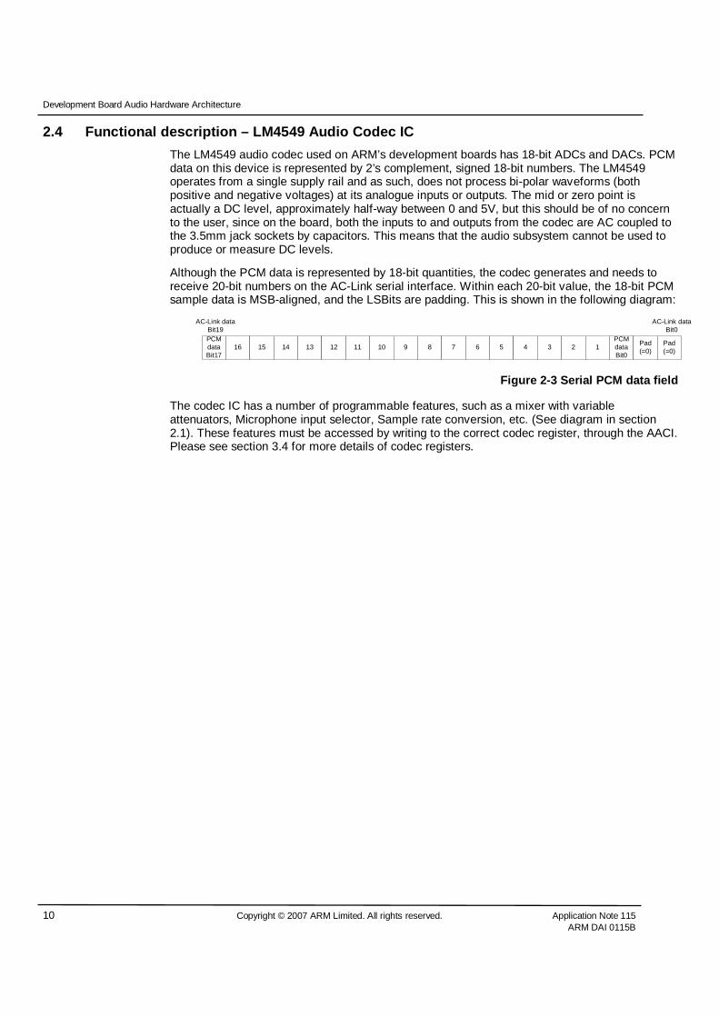
Although the PCM data is represented by 18-bit quantities, the codec generates and needs toreceive 20-bit numbers on the AC-Link serial interface. Within each 20-bit value, the 18-bit PCMsample data is MSB-aligned, and the LSBits are padding. This is shown in the following diagram:
PCMdataBit17
16 15 14 13 12 11 10 9 8 7 6 5 4 3 2 1PCMdataBit0
Pad(=0)
Pad(=0)
AC-Link dataBit19
AC-Link dataBit0
Figure 2-3 Serial PCM data field
The codec IC has a number of programmable features, such as a mixer with variableattenuators, Microphone input selector, Sample rate conversion, etc. (See diagram in section2.1). These features must be accessed by writing to the correct codec register, through the AACI.Please see section 3.4 for more details of codec registers.
The following algorithms describe the ‘bare minimum’ set-up required to make the audiosubsystem process audio data in the receive and transmit (record and playback) directions. Thisset-up procedure assumes that all AACI registers are in their default states, as would be the caseafter a reset. This means that the default ‘Non-Compact mode’ with 18-bit resolution is used.
Note that the register names listed here and in the example code may have one or moreunderscore ‘_’ characters inserted to assist readability. The true register names, as written in theAACI TRM are usually the same, but without the underscores.
• Reset the codec IC. This is done by setting bit0 in the AACI’s AACI_RESET register thenclearing it. The value in bit0 of the register is reflected on the AACI_RESET output pinfrom the AACI, which resets the Codec. The accompanying demo code generates areset pulse of 100ms
• To enable audio recording - Program AACI_RXCR1 register to associate the RX FIFOwith the relevant AC-Link slots, namely Slot3 for Right channel data and Slot4 for theLeft channel. The receive FIFO is enabled in the same register
• To enable audio playback - Program the AACI_TXCR1 register to associate the TX FIFOwith the relevant audio data slots, and enable transmit FIFO as for receive above
• To enable programming of the Codec IC and operation of the audio subsystem -Program the AACI_MAINCR register to enable Slot1 (Command address), Slot2(Command data) and to enable the AACI
• Program Codec volume control, mixer input select, bit rate, etc. as required. This is doneby writing the required codec control data and associated register address values to theAACI_SL2TX and AACI_SL1TX registers respectively. The registers must be performedin that order, and only when the associated busy flags in the AACI_SLFR register areclear. Codec reset default settings are: All volume/gain controls at 0dB but muted, recordinput = MIC1, record and playback sample rates fixed at 48kHz
• Play audio data by repeatedly placing sample values into the transmit FIFO, which isaccessed by writing to register AACI_DR1. This should only be done when theAACI_TXFF flag in the AACI_SR1 register is clear, indicating that the FIFO is not full.The AACI will automatically send the samples to the codec at the programmed samplerate
• Record audio data by retrieving sample values from the receive FIFO and storing themin system memory. This is done by reading register AACI_DR1. The register should onlybe read when the receive FIFO is not empty; indicated by the AACI_RXFE flag in theAACI_SR1 register. Samples will be placed in the FIFO at the selected sample rate.
The simple example code supplied with this Apps Note demonstrates the above procedures.
3.2 Working with different audio sample data widths
3.2.1 Processing 12, 16, 18 or 20-bit data
The AACI PrimeCell which drives and controls the codec has the ability to process 12, 16, 18 or20-bit PCM data in hardware. The reset default is 16-bit. The codec IC only works with 18-bitdata packed into 20-bit numbers, so the AACI can convert sample data as follows:
Recording
The AACI discards some of the least significant bits of the incoming samples by right-shifting thereceived 20-bit values so that the resultant data is least-significant bit justified.
The number of bits discarded depends on which sample data size is selected in the AACI. This isset by the ‘TSize’ bits in the AACITXCR1 register. For example, with the AACI set to 16-bitmode, the least significant 4 bits of the 20-bit data words from the codec are discarded,producing 16-bit numbers. This has the effect of reducing the resolution of the recorded audiodata from 18-bits to 16-bits.
Playback
Again, the AACI can be configured to work with 12, 16, 18 or 20-bit PCM data. The AACI MSB-justifies the PCM data from the ARM into 20-bit numbers, by left-shifting the sample data asrequired, and padding the least significant bits with zeros. Using the example of 16-bit dataagain, the AACI would left-shift sample values by 4 bits and insert 4 zero bits of padding beforesending the data to the codec.
The highest audio resolution possible on the development system therefore is 18 bits. If 20-bitdata is sent to the codec, it will ignore the LS 2 bits. If the AACI is set to receive 20-bit samplesfrom the codec, only 18 bits of resolution will be achieved, since the LS 2 bits from the codec willalways be zero.
3.2.2 Processing sub 12-bit PCM data
The lowest resolution PCM data that the AACI can process in hardware is 12 bits per sample, soan 8-bit data stream needs some extra work to be done by the ARM processor.
Playback
Sample data needs to be MSB-justified into the data size selected in the AACI. For example, ifthe AACI is set to 16-bit, each 8-bit sample needs to be left-shifted by eight places before beingsent to the AACI.
To complicate matters slightly, 8-bit PCM data contained in WAV files is usually stored asunsigned numbers, whereas the LM4549 codec (and most 16-bit WAV files) work with signedquantities. Attempting to play unsigned samples directly will produce a horribly distortedwaveform, since any part of the waveform which exceeds the maximum value which can berepresented as a 2’s complement number will wrap around and appear at the opposite end of thewaveform.
Thus, when playing unsigned sample data, an offset which corresponds to the mid-point valuemust be deducted from each sample value before left-shifting. For 8-bit unsigned values, thisoffset is 0x7F.
Recording
To convert for example, 16-bit samples from the AACI into 8-bit PCM data, the sample valueswould need to be right-shifted by 8 places, to reduce the resolution to 8 bits. If it is necessary to
convert 8-bit signed values into unsigned values, an offset of 0x7F would then need to be addedto each sample.
3.3 Working with monophonic audio data
There is no hardware setting in the Codec which causes it to process only monophonic audio, butthere are several ways to implement mono sound.
Perhaps the most obvious method would be to se-up the AACI to process stereo audio data asnormal, but only make use of one analogue audio channel. When recording, the unwanted audiochannel data could simply be discarded. On playback, the ARM would have to supply dummydata for the unused channel, so that all FIFO locations were occupied. This method has aproblem in that it uses twice as much bus and CPU bandwidth than is actually needed.
A better (and simpler) solution is to only set-up the AACI to process data for one of the twoavailable audio channels. The AACI then no longer interleaves Left and Right samples, butassociates each sequential parallel data word with the same audio channel. To do this, only theLeft audio channel (AC-Link Slot 3) should be enabled in the AACI_TXCR1 or AACI_RXCR1registers. This method does not work if only the Right channel (Slot 4) is enabled. Note that ifsample data with interleaved stereo samples is played with the AACI setup in this way, theresultant mono audio output will contain both L and R channel data, so will appear to be playingat half speed.
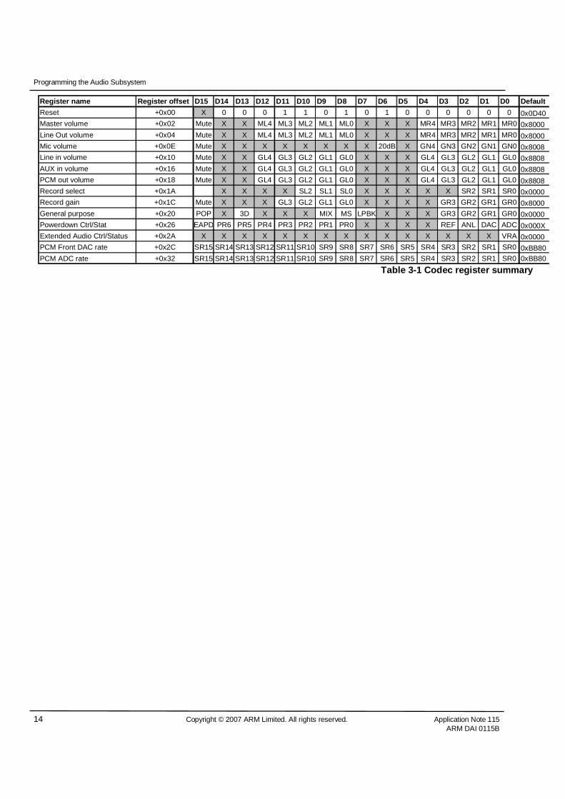
3.4 Programmable features of the LM4549 codec
The LM4549 codec contains a number of registers which can be programmed via the AC-Linkinterface, from the AACI PrimeCell. These allow software control of such features as mixer gainsettings and ADC/DAC sample rates. This section contains a table which lists only the codecregisters that have effect or use on the ARM development boards. Following the table, there is abrief description of the registers, and the bit slices within the registers. For more informationplease see the data sheet for the codec chip.
The codec registers are accessed by writing the required address and data values into AACIregisters AACISL1TX and AACISL2TX respectively. These registers correspond to AC-Link timeslots 1 and 2, which are the ‘Command Address’ and ‘Command Data’ slots. Transmission mustfirst be enabled by setting the ‘Sl1TxEn’ and ‘Sl2TxEn’ bits in the AACIMAINCR register. See theAACI TRM for exact details.
The example C source code supplied with this Apps Note shows how to perform theseoperations. Please see section 4.2 for further details.
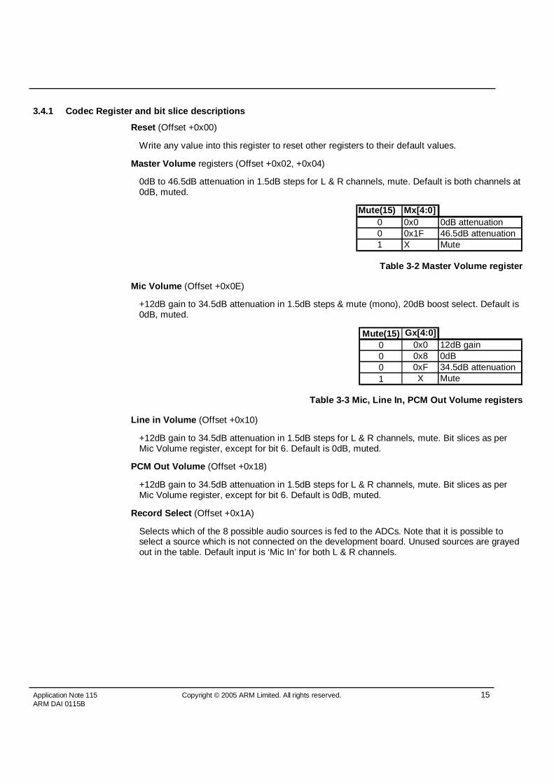
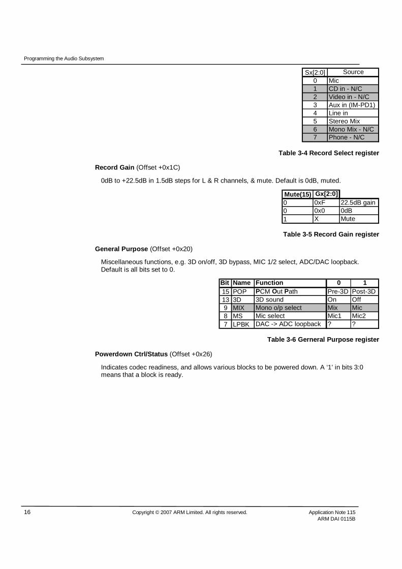
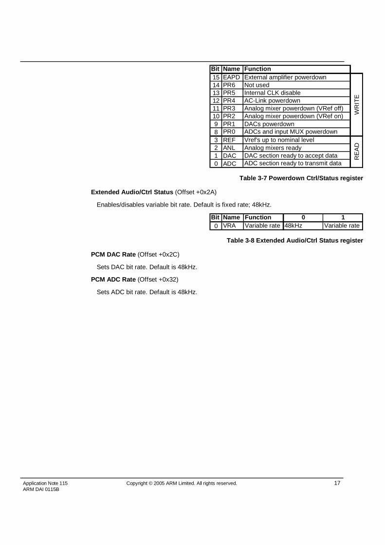
Reset +0x00 X 0 0 0 1 1 0 1 0 1 0 0 0 0 0 0 0x0D40Master volume +0x02 Mute X X ML4 ML3 ML2 ML1 ML0 X X X MR4 MR3 MR2 MR1 MR0 0x8000Line Out volume +0x04 Mute X X ML4 ML3 ML2 ML1 ML0 X X X MR4 MR3 MR2 MR1 MR0 0x8000Mic volume +0x0E Mute X X X X X X X X 20dB X GN4 GN3 GN2 GN1 GN0 0x8008Line in volume +0x10 Mute X X GL4 GL3 GL2 GL1 GL0 X X X GL4 GL3 GL2 GL1 GL0 0x8808AUX in volume +0x16 Mute X X GL4 GL3 GL2 GL1 GL0 X X X GL4 GL3 GL2 GL1 GL0 0x8808PCM out volume +0x18 Mute X X GL4 GL3 GL2 GL1 GL0 X X X GL4 GL3 GL2 GL1 GL0 0x8808Record select +0x1A X X X X SL2 SL1 SL0 X X X X X SR2 SR1 SR0 0x0000Record gain +0x1C Mute X X X GL3 GL2 GL1 GL0 X X X X GR3 GR2 GR1 GR0 0x8000General purpose +0x20 POP X 3D X X X MIX MS LPBK X X X GR3 GR2 GR1 GR0 0x0000Powerdown Ctrl/Stat +0x26 EAPD PR6 PR5 PR4 PR3 PR2 PR1 PR0 X X X X REF ANL DAC ADC 0x000XExtended Audio Ctrl/Status +0x2A X X X X X X X X X X X X X X X VRA 0x0000PCM Front DAC rate +0x2C SR15 SR14 SR13 SR12 SR11 SR10 SR9 SR8 SR7 SR6 SR5 SR4 SR3 SR2 SR1 SR0 0xBB80PCM ADC rate +0x32 SR15 SR14 SR13 SR12 SR11 SR10 SR9 SR8 SR7 SR6 SR5 SR4 SR3 SR2 SR1 SR0 0xBB80
+12dB gain to 34.5dB attenuation in 1.5dB steps for L & R channels, mute. Bit slices as perMic Volume register, except for bit 6. Default is 0dB, muted.
PCM Out Volume (Offset +0x18)
+12dB gain to 34.5dB attenuation in 1.5dB steps for L & R channels, mute. Bit slices as perMic Volume register, except for bit 6. Default is 0dB, muted.
Record Select (Offset +0x1A)
Selects which of the 8 possible audio sources is fed to the ADCs. Note that it is possible toselect a source which is not connected on the development board. Unused sources are grayedout in the table. Default input is ‘Mic In’ for both L & R channels.
Sx[2:0] Source0 Mic1 CD in - N/C2 Video in - N/C3 Aux in (IM-PD1)4 Line in5 Stereo Mix6 Mono Mix - N/C7 Phone - N/C
Table 3-4 Record Select register
Record Gain (Offset +0x1C)
0dB to +22.5dB in 1.5dB steps for L & R channels, & mute. Default is 0dB, muted.
Mute(15) Gx[2:0]0 0xF 22.5dB gain0 0x0 0dB1 X Mute
Table 3-5 Record Gain register
General Purpose (Offset +0x20)
Miscellaneous functions, e.g. 3D on/off, 3D bypass, MIC 1/2 select, ADC/DAC loopback.Default is all bits set to 0.
Bit Name Function 0 115 POP PCM Out Path Pre-3D Post-3D13 3D 3D sound On Off9 MIX Mono o/p select Mix Mic8 MS Mic select Mic1 Mic27 LPBK DAC -> ADC loopback ? ?
Table 3-6 Gerneral Purpose register
Powerdown Ctrl/Status (Offset +0x26)
Indicates codec readiness, and allows various blocks to be powered down. A ‘1’ in bits 3:0means that a block is ready.
This section describes the example source code which is available for the audio subsystem onARM development boards.
4.1 PrimeCell driver software
Some ARM development systems, namely the Integrator/CP and Integrator/IM-PD1 boards wereoriginally supplied with the PrimeCell driver C source code on CD. This software was suppliedunder a development license, which meant that it could not be used in an application without aspecific license agreement from ARM.
The PrimeCell driver code supplied with these ARM development boards is arranged into amenu-driven test program for all of the PrimeCell peripherals on the development board.
For many developers, this is not a good starting point for simply trying to get the audio codecworking, since there are several layers of abstraction within the source code, and the programitself uses several levels of buffering for the audio data. The PrimeCell AACI driver code isinterrupt driven and the interrupt handler code is large, since it contains code for all theperipheral interrupt sources. These factors can make it difficult to extract the relevantinformation about how the audio subsystem should be programmed.
With this in mind, we have created some simple demonstration code, which is described below:
4.2 Simple AACI example code
Due to the complexity of the PrimeCell driver code, we have provided some very simple, non-interrupt driven code which demonstrates how to set up the AACI and codec IC to perform basicrecord and playback functions. This code is based on the self-test code shipped with thedevelopment boards, and is available for download from the ARM website, along with thisApplications Note.
The simple example code demonstrates how to perform the following operations:
• Simple, ‘bare minimum’ set-up for the AACI and codec
• Software control of codec chip mixer level controls for Master volume, PCM playbackvolume, Record gain, ADC and DAC rates
• Playback a 16-bit stereo PCM data clip. The clip must have been previously stored inflash memory using the flash programming facilities in the ARM debugger or BootMonitor. For details on how to do this, see section 4.3.
• Record an audio clip from the MIC1 input into RAM, and then play back that clip
• Play a sine wave tone from a lookup table. Frequency can be changed by adjusting theDAC playback rate.
There is a single set of example source files which can be built to run on one of the platformslisted at the start of section 1 by performing the following steps:
1. Extract the Apps Note demonstration code into a clean directory.
2. Run the batch file which pertains to your development board, e.g. buildAP.bat,buildCP.bat or buildVP.bat. The batch files call the ARM code generation tools withthe correct command line options to build the code for your chosen board.
For a full list of files included with this Applications Note, see section 4.5. The code is not builtfor any particular ARM core type, so the resultant executable is ARM architecture v4 machinecode, and does not attempt to make use of cache memories. It makes no use of interrupts,instead polling various status flag registers in the AACI before processing data. One of thetimer/counter modules on the chosen platform board are used for timeout and sleep functions,and again this is polled rather than interrupt driven. This arrangement means that when the ARMcore is not actually transferring audio data between system memory and the audio subsystem, itis simply spinning cycles, waiting for the timer to time out.
4.3 DMA Audio example code (DMAC-equipped boards only)
The following boards contain a PrimeCell DMA Controller, which once initialized can be used tosend data to/from the AACI without constant intervention from the CPU:
BoardType
PrimeCell DMAC DMACLocation
AB926EJ-S PL080 Dev Chip
PB926EJ-S PL080 Dev Chip
EB* PL081 FPGA
Table 4-1 DMAC PrimeCell part number and physical location
* Whether a DMAC is present in an EB-based system depends largely on the version of theFPGA image. The FPGA must be re-programmed for each different type of Core Tile used withthe EB. Please refer to the Application Note that relates to your specific EB FPGA build forinformation on the presence of a DMA Controller.
The following build batch files will produce executable code that contains the DMAdemonstration:
• BuildAB926.bat
• BuildPB926.bat
• BuildEB.bat
These builds of the example code demonstrate use of a DMAC to transfer a pre-recorded audioclip from Flash memory to the AACI.
The supplied DMA example code can be run by choosing the relevant item from the AACIdemonstration program menu. Only one DMA demonstration is included, which plays a fixedlength selection of PCM audio data from the Line Out socket on the development board. Theaudio data must previously have been stored in Flash memory at the address used by thespecific build of the program:
Build Flashaddress
xB926EJ-S 0x36000000
EB 0x43800000
Table 4-2 Flash memory location for pre-recorded audio clip
If the Flash is not pre-programmed with the audio clip data, the AACI will try to ‘play’ whatevernumerical values are stored in Flash. This might amount to nothing if the Flash is erased, orsomething approximating white noise if the Flash contains program opcodes. For details of howto program PCM audio data into flash, please see section 4.4.
Note: None of the Integrator systems available ‘off-the-shelf’ contains a DMA controller, althoughit would be possible for a developer to add one, were there enough free FPGA resourceavailable in the system. For this reason, this DMA example code does not have build options forIntegrator boards.
The example code sets up the DMAC to perform memory to peripheral transfers, with the DMACas the flow controller. This means that the DMAC performs a finite number of preprogrammedtransfers. If the DMAC were configured for Memory -> Peripheral transfer with the peripheral asthe flow controller, the AACI would never stop playing audio, since it has no way of knowingwhen the audio data has all been played and would continue to request bursts of data from theDMAC indefinitely.
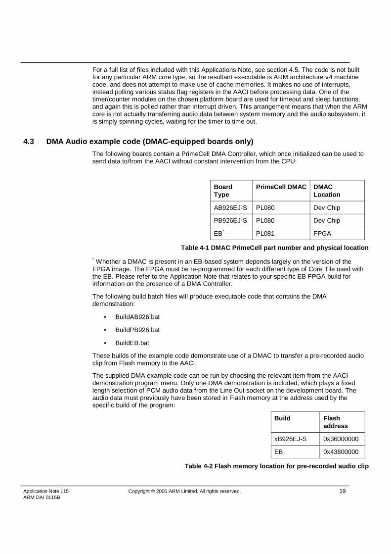
4.3.1 xB926EJ-S bus architecture and DMA data transfer path
The AB926EJ-S and PB926EJ-S development boards utilize the same ‘Development Chip’, inwhich there is an ARM926EJ-S processor core, some peripherals and a 6-layer bus matrix. Thismaximizes data throughput since bus transactions can take place between devices on differentlayers of the bus simultaneously. In summary:
1. The ARM926EJ-S core fetches and executes the program instructions from the SDRAMcontroller on the ARM Instruction-AHB bus layer.
2. The ARM writes configuration data to the DMAC’s slave port on the ARM Data-AHB buslayer. (There are also writes to the SSRAM area (SSMC) when the LLI table ispopulated, but this is not shown for clarity.)
3. Once enabled, the DMAC fetches data from the Flash memory (SSMC) using its AHB1master port…
4. …and writes the same data out of its AHB2 master port to the AACI in the board’sFPGA. This data exits the Dev. Chip on the external ‘M2’ bus.
Items 3 and 4 above are repeated until the DMAC has transferred the last block of data to theAACI. This is shown in the following diagram:
Figure 4-1 xB926EJ-S bus architecture and DMA data path
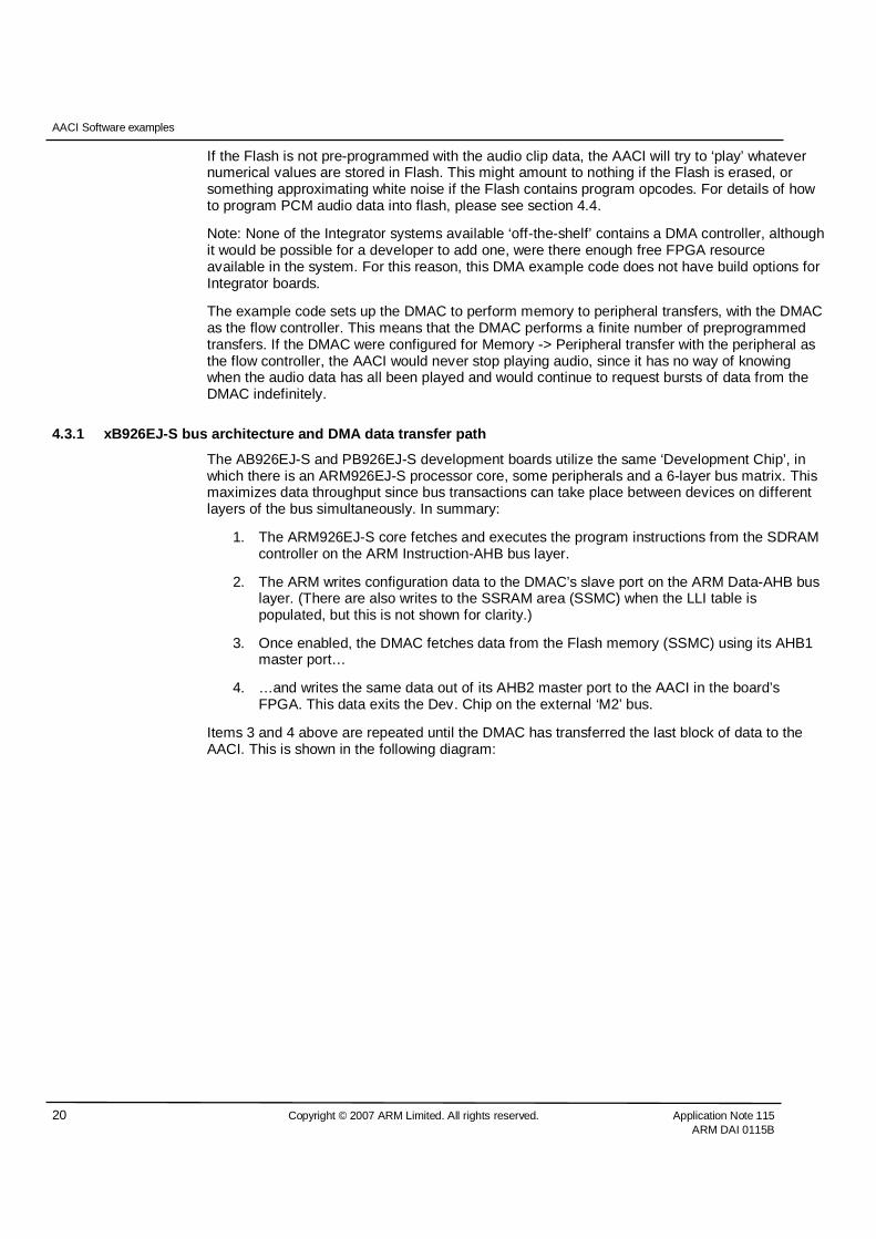
4.3.2 DMA handshake signal routing on the PB926EJ-S
The PL080 DMAC has eight separate ‘channels’ which can be used to configure and control eightseparate DMA transfer sequences to/from memory or peripherals. It also has sixteen sets ofperipheral handshaking lines, so can be connected to a maximum of sixteen peripheral devicesin a system. A ‘channel’ can be programmed to manage a DMA transfer sequence between twospecific devices, and then it can be re-programmed for another transfer sequence.
In the PB926EJ-S system there are more than 16 devices that have DMA handshaking signals,and the lowest three handshaking signals (0, 1, 2) into the DMAC are shared between a numberof peripheral devices in the PB926 FPGA and up to 3 devices in an attached logic tile. The threeDMA signals from the logic tile stack are always connected to DMAC request lines 0, 1, 2. Inaddition, there are three multiplexers in the PB926 FPGA which can be configured (by theSYS_DMAPSRx registers in the FPGA) to connect any three of the ten devices in the FPGA tothe DMAC.
These are: AACI Rx and TX, USB ‘A’ and ‘B’, MMCI 0 and 1. It is important that the logic tile andFPGA do not drive the same DMA request line.
This multiplexing arrangement is shown in the following diagram:
Example code configuresSYS_DMAPSR0 registerto connect AACI Tx transferrequest signals to the DMAC
Figure 4-2 DMA handshake signal MUXing on the PB926EJ-S
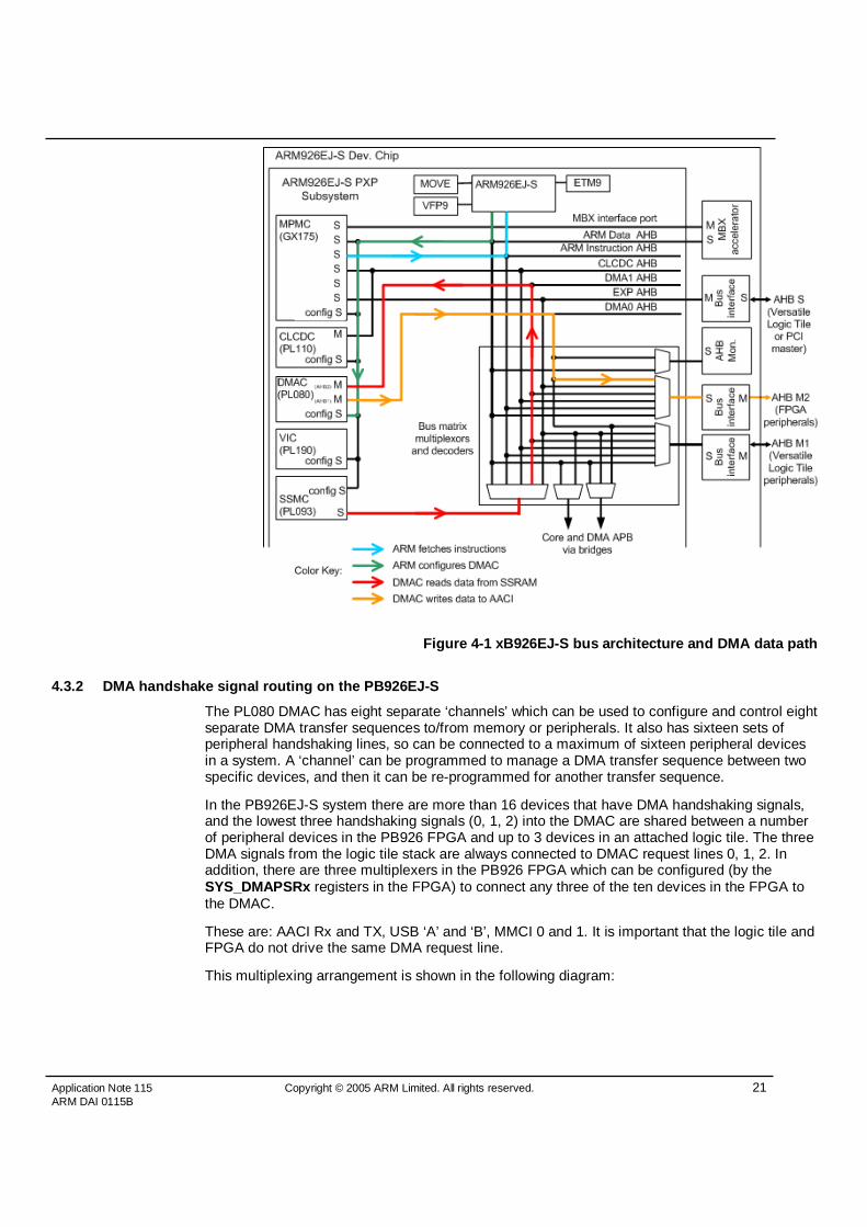
4.3.3 DMA handshake signal routing on the AB926EJ-S
The AB926EJ-S board uses the same Dev Chip as the PB926EJ-S board, and also uses thesame PL080 DMAC inside its FPGA. The DMA handshake signal routing differs between the twoboards however. Since the AB926EJ-S board has a reduced feature set from the PB926EJ-Sboard, it is not possible to perform DMA transfers with the same range of peripherals. DMAhandshake signal routing is fixed and there are no SYS_DMAPSRx registers. The mapping is asfollows:
DMAC Peripheral # Peripheral
0 AACI Rx
1 AACI Tx
2 MCI0
Figure 4-3 DMAC Peripheral numbers on the AB926EJ-S
Attempts to access the non-existent SYS_DMAPSRx registers will not result in any kind of buserror since the AHB-APB bridge returns an OKAY response to all transfers; even if the LSbits of
the address do not decode to anything. The example software utilizes this fact to make the codesimpler, as the same code can be used for both the AB and PB926 boards.
4.3.4 EB bus architecture and DMA data transfer path
The bus architecture of an EB system is defined by the image programmed into the EB FPGA.The following diagram is from the Applications Note AN152 - Using a CT11MPCore with theRealViewTM Emulation Baseboard. Either an AXI or AHB bus matrix will be employed,depending on which ARM core type the FPGA image was designed to work with. Please refer tothe Applications Note that relates to your system configuration for exact details.
Data flow is very similar to the xB926EJ-S systems, but EB systems use a single-master DMAC.
1. The ARM core fetches and executes the program instructions from the SDRAMcontroller
2. The ARM writes configuration data to the DMAC's slave port on the ARM Data-AHB buslayer. (There are also writes to the SSRAM area (SSMC) when the LLI table ispopulated, but this is not shown for clarity.)
3. Once enabled, the DMAC fetches data from the Flash memory (SSMC)...
4. …and writes the same data out to the AACI.
The following diagram shows the general data flow in an EB system:
The EB uses a similar multiplexing system to the PB926EJ-S, with some peripherals connecteddirectly to the DMAC and some being multiplexed with the Logic Tile DMA lines. Fortunately forthis application, the AACI DMA lines have exclusive connections to the DMAC in the FPGA. Thismakes the set-up code simpler.
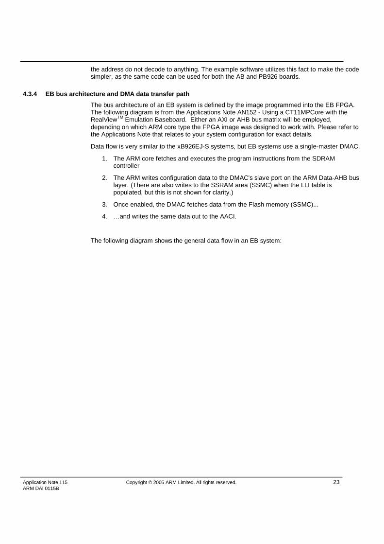
The following table shows some of the DMAC to Peripheral connections in an EB FPGA image:
[6:15] Other peripherals - see user guide if interested
Figure 4-5 DMAC Peripheral numbers on the EB
4.3.6 Use of linked lists to transfer a large block of data
There is a hierarchy to the way in which data is transferred by the DMAC. An entirepreprogrammed transfer sequence is split up into one or more DMA ‘packets’. One packet ismade up of a maximum of 4095 ‘transfers’ (transactions on the AMBA bus), which can begrouped together in ‘bursts’ of up to 256 transfers. Note that it is not possible to directly specifywhich kind of AMBA burst (E.g. AHB burst types: INCR, INCR4, INCR8 - as indicated by theHBURST signals) is generated; the DMAC decides which AMBA transfer type to use.
The PL080 and PL081 DMACs used on the xB926EJ-S and EB systems are AHB devices.Where an AXI bus matrix is used in the EB FPGA, an AHB-AXI bridge is employed for protocolconversion (see Figure 4-4).
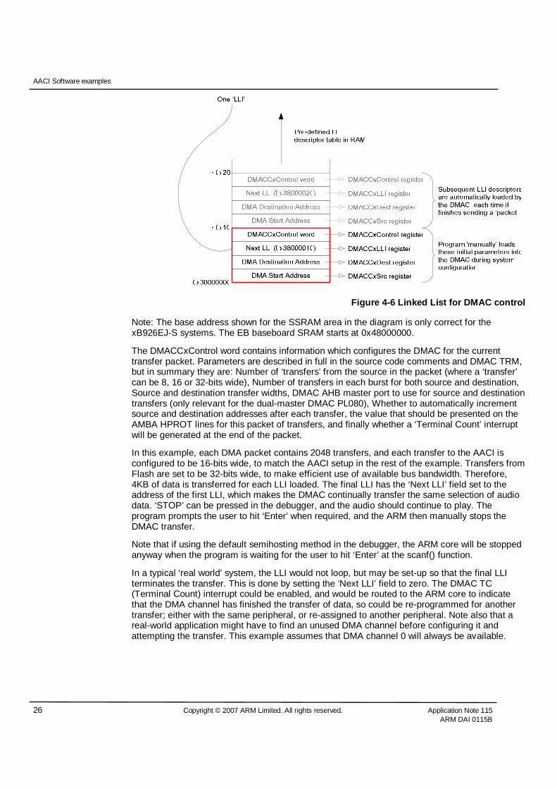
If more than one packet of data is to be transferred, this can be automated by generating alinked list in memory, which contains a series of 4-word descriptors or LLIs (Linked List Items)that tell the DMAC where to get the data from, where to send it, where to find the next LLI, andother options for transfer of the packet. Once initialized, the DMAC automatically loads LLIs frommemory until it loads an LLI which tells it to stop transferring data, or the DMAC is manuallydisabled.
This code example creates a circular linked list in the baseboard SRAM area before it configuresthe DMAC. Once enabled, the DMAC follows the linked list, playing a loop of audio until the userinstructs the program to disable the DMAC transfer.
Each linked list item (LLI) contains the following data:
Note: The base address shown for the SSRAM area in the diagram is only correct for thexB926EJ-S systems. The EB baseboard SRAM starts at 0x48000000.
The DMACCxControl word contains information which configures the DMAC for the currenttransfer packet. Parameters are described in full in the source code comments and DMAC TRM,but in summary they are: Number of ‘transfers’ from the source in the packet (where a ‘transfer’can be 8, 16 or 32-bits wide), Number of transfers in each burst for both source and destination,Source and destination transfer widths, DMAC AHB master port to use for source and destinationtransfers (only relevant for the dual-master DMAC PL080), Whether to automatically incrementsource and destination addresses after each transfer, the value that should be presented on theAMBA HPROT lines for this packet of transfers, and finally whether a ‘Terminal Count’ interruptwill be generated at the end of the packet.
In this example, each DMA packet contains 2048 transfers, and each transfer to the AACI isconfigured to be 16-bits wide, to match the AACI setup in the rest of the example. Transfers fromFlash are set to be 32-bits wide, to make efficient use of available bus bandwidth. Therefore,4KB of data is transferred for each LLI loaded. The final LLI has the ‘Next LLI’ field set to theaddress of the first LLI, which makes the DMAC continually transfer the same selection of audiodata. ‘STOP’ can be pressed in the debugger, and the audio should continue to play. Theprogram prompts the user to hit ‘Enter’ when required, and the ARM then manually stops theDMAC transfer.
Note that if using the default semihosting method in the debugger, the ARM core will be stoppedanyway when the program is waiting for the user to hit ‘Enter’ at the scanf() function.
In a typical ‘real world’ system, the LLI would not loop, but may be set-up so that the final LLIterminates the transfer. This is done by setting the ‘Next LLI’ field to zero. The DMAC TC(Terminal Count) interrupt could be enabled, and would be routed to the ARM core to indicatethat the DMA channel has finished the transfer of data, so could be re-programmed for anothertransfer; either with the same peripheral, or re-assigned to another peripheral. Note also that areal-world application might have to find an unused DMA channel before configuring it andattempting the transfer. This example assumes that DMA channel 0 will always be available.
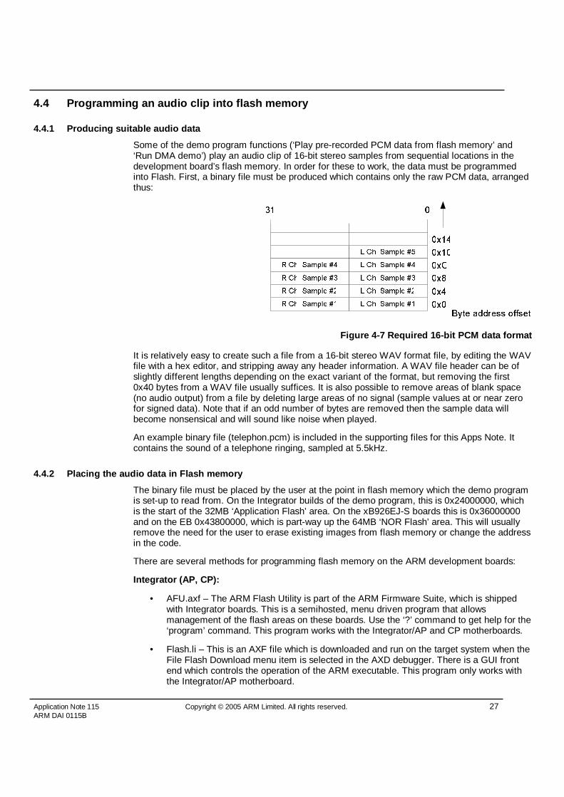
Some of the demo program functions (‘Play pre-recorded PCM data from flash memory’ and‘Run DMA demo’) play an audio clip of 16-bit stereo samples from sequential locations in thedevelopment board’s flash memory. In order for these to work, the data must be programmedinto Flash. First, a binary file must be produced which contains only the raw PCM data, arrangedthus:
Figure 4-7 Required 16-bit PCM data format
It is relatively easy to create such a file from a 16-bit stereo WAV format file, by editing the WAVfile with a hex editor, and stripping away any header information. A WAV file header can be ofslightly different lengths depending on the exact variant of the format, but removing the first0x40 bytes from a WAV file usually suffices. It is also possible to remove areas of blank space(no audio output) from a file by deleting large areas of no signal (sample values at or near zerofor signed data). Note that if an odd number of bytes are removed then the sample data willbecome nonsensical and will sound like noise when played.
An example binary file (telephon.pcm) is included in the supporting files for this Apps Note. Itcontains the sound of a telephone ringing, sampled at 5.5kHz.
4.4.2 Placing the audio data in Flash memory
The binary file must be placed by the user at the point in flash memory which the demo programis set-up to read from. On the Integrator builds of the demo program, this is 0x24000000, whichis the start of the 32MB ‘Application Flash’ area. On the xB926EJ-S boards this is 0x36000000and on the EB 0x43800000, which is part-way up the 64MB ‘NOR Flash’ area. This will usuallyremove the need for the user to erase existing images from flash memory or change the addressin the code.
There are several methods for programming flash memory on the ARM development boards:
Integrator (AP, CP):
• AFU.axf – The ARM Flash Utility is part of the ARM Firmware Suite, which is shippedwith Integrator boards. This is a semihosted, menu driven program that allowsmanagement of the flash areas on these boards. Use the ‘?’ command to get help for the‘program’ command. This program works with the Integrator/AP and CP motherboards.
• Flash.li – This is an AXF file which is downloaded and run on the target system when theFile Flash Download menu item is selected in the AXD debugger. There is a GUI frontend which controls the operation of the ARM executable. This program only works withthe Integrator/AP motherboard.
• Integrator Boot Monitor ‘L’ command – The boot monitor program installed in Flash onthe Integrator/AP and CP motherboards. It is possible to transfer data from a hostmachine to the Integrator motherboards across an RS232 connection, but this is notrecommended since it is very slow. See the user guide for the Integrator system formore information.
Versatile (xB926EJ-S):
• RVD’s built-in Flash programming functionality – RVD (RealView Debugger) has a built-in Flash programmer, which is invoked whenever the user tries to update the contents ofmemory which is defined as being Flash memory in a ‘board file’. The ‘DebugMemory/Register Operations Upload/Download Memory file’ menu option can be used tofill an area of memory from a disk file.
Versatile (EB, xB926EJ-S):
• V/PB Boot monitor (v1.1 onwards). First, the Flash submenu must be entered by typing‘flash’ at the boot monitor prompt, followed by <Return>. Then use the ‘write binary’command to place the audio data into Flash. Example command sequence:
Note 1: Using the boot monitor it is possible to program the Flash on the xB926EJ-Sboards using Multi-ICE, RealVIEW ICE or the built-in USB debug port. With the EB, onlyRealView ICE can be used.
Note 2: Later versions of the Versatile Boot Monitor allow an MMC or SD card, mountedas a drive letter to be used as the source for the Flash> write binary and write imagecommands. Please refer to the baseboard user guide for further information.
• Network Flash Utility (NFU). This utility is available on the CD-ROM that ships with theboards. It must be installed and run from Flash, and allows the user to program Flashmemory on the baseboard from files on a TFTP server. The command line interface isvery similar to the Boot Monitor ‘Flash>’ sub-menu and instructions can be found in thebaseboard user guides.
4.4.3 Playing MP3 or WAV format files
It is possible to make the development board play WAV files directly (without first stripping andinterpreting the header information), provided there are an even number of bytes in the filebefore the audio data starts. The header information at the start of the file will simply appear as abrief ‘pop’ from the speakers. To play WAV files properly, code should be included to strip theheader information from start of the file, leaving just the PCM data. Code could also be written tointerpret the WAV file header and program the AACI and codec accordingly for the correct bitrate, number of channels and resolution.
Other audio file formats, e.g. MP3 could be processed if an appropriate software codec for theARM processor were obtained. ARM does not currently provide such software.
4.5 List of files included in the ‘Applications Note 115’ zip file
These are the files included in the demo code zip file:
audiodemo.c The main Audio demonstration program, containing the C ‘main()’ function, which provides arudimentary, ‘semihosting’-driven menu system that calls the various demonstration and testroutines.
audiodemo.h Header file which defines some global variables and pointers used by the main() and aacifunctions.
aaci.c Contains functions illustrating how to set-up and control the AACI and Codec, and how to makethe system play and record PCM audio data.
aaci.h Header file containing register addresses and miscellaneous definitions for the PrimeCellPL041 AACI and LM4549 Codec.
dma.c Contains functions specific to the initialization of the DMA controller.
dma.h Header file containing register addresses and miscellaneous definitions for the PrimeCellPL080 DMA Controller.
common.c Sleep/timeout functions with board-specific implementations
common.h Header file for common.c, containing addresses for timer peripheral etc.
BuildAP.bat MS-DOS batch file to call the ARM software development tools to build this example code foran Integrator/AP + LM + IM-PD1 system.
BuildCP.bat Batch file to build the AACI example code for an Integrator/CP system.
BuildAB926.bat Batch file to build the example code for an AB926EJ-S system.
BuildPB926.bat Batch file to build the example code for a PB926EJ-S system.
BuildEB.bat Batch file to build the example code for an EB system.
AN115.pdf This document.
telephon.pcm PCM audio file containing the sound of a UK telephone ringing once. Stereo recording, but froma mono source. 5.5kHz sample rate, 16-bit samples.
The source files are well commented, so are not explained in any detail here. The larger headerfiles are cut-down versions of files supplied with the development boards, on CD-ROM. Only theregister address and function definitions pertinent to this demo are included in these files, inorder to aid understanding. Please refer to the full header files supplied on the board CDs if youneed to add extra functionality to this demo code.