electronics Article Design, Simulation and Hardware Implementation of Shunt Hybrid Compensator Using Synchronous Rotating Reference Frame (SRRF)-Based Control Technique R. Balasubramanian, K. Parkavikathirvelu, R. Sankaran and Rengarajan Amirtharajan * School of Electrical & Electronics Engineering (SEEE)S, SASTRA Deemed University, Thirumalaisamudram, Thanjavur 613401, India; [email protected] (R.B.); [email protected] (K.P.); [email protected] (R.S.) * Correspondence: [email protected]; Tel.: +91-4362-264101 Received: 26 September 2018; Accepted: 21 December 2018; Published: 1 January 2019 Abstract: This paper deals with the design, simulation, and implementation of shunt hybrid compensator to maintain the power quality in three-phase distribution networks feeding different types balanced and unbalanced nonlinear loads. The configuration of the compensator consists of a selective harmonic elimination passive filter, a series-connected conventional six-pulse IGBT inverter, acting as the active filter terminated with a DC link capacitor. The theory and modelling of the compensator based on current harmonic components at the load end and their decomposition in d-q axis frame of reference are utilized in the reference current generation algorithm. Accordingly, the source current waveform is made to follow the reference current waveform using a high-frequency, carrier-based controller. Further, this inner current control loop is supported by a slower outer voltage control loop for sustaining desirable DC link voltage. Performance of the compensator is evaluated through MATLAB simulation covering different types of loads and reduction of harmonic currents and THD at the supply side along with excellent regulation of DC link voltage are confirmed. The performance of a hybrid compensator designed and fabricated using the above principles is evaluated and corroborated with the simulation results. Keywords: harmonics; hybrid power filter; active power filter; power quality; total harmonic distortion 1. Introduction One major area of research that has gained attention in recent times is maintaining power quality of distribution systems. The power quality issues arise due to the widespread usage of processed power in industrial applications and commercial/domestic applications [1–3]. For example, variable speed drives are implemented through power modulators which consist of high-power controlled/uncontrolled rectifiers feeding variable voltage and variable frequency multiphase inverters. Similarly, commercial power consumption is characterised by appliances like computers, photocopiers, and fax machines, along with fluorescent and CFL lamps. All the above represent nonlinear loads, resulting in lower supply-side power factor and waveform distortion, indicated by harmonic components in voltage and current. The adverse effect of harmonics includes heating and extra losses, saturation and malfunctioning of distribution transformers, interference with communication signals, damages to consumer utilities, and in extreme cases, the failure of supply-side equipment [4]. The initial steps towards mitigation of the above problems were focused on the low power factor at the supply side only, whereby a passive power filter (PPF) connected in shunt compensates for the lagging reactive current, which was extended with selective harmonic elimination. The disadvantage of this approach is insensitivity with load current changes and fluctuations in supply-side voltage. Electronics 2019, 8, 42; doi:10.3390/electronics8010042 www.mdpi.com/journal/electronics
Transcript
electronics
Article
Design, Simulation and Hardware Implementation ofShunt Hybrid Compensator Using SynchronousRotating Reference Frame (SRRF)-BasedControl Technique
R. Balasubramanian, K. Parkavikathirvelu, R. Sankaran and Rengarajan Amirtharajan *
Received: 26 September 2018; Accepted: 21 December 2018; Published: 1 January 2019
Abstract: This paper deals with the design, simulation, and implementation of shunt hybridcompensator to maintain the power quality in three-phase distribution networks feeding differenttypes balanced and unbalanced nonlinear loads. The configuration of the compensator consists of aselective harmonic elimination passive filter, a series-connected conventional six-pulse IGBT inverter,acting as the active filter terminated with a DC link capacitor. The theory and modelling of thecompensator based on current harmonic components at the load end and their decomposition ind-q axis frame of reference are utilized in the reference current generation algorithm. Accordingly,the source current waveform is made to follow the reference current waveform using a high-frequency,carrier-based controller. Further, this inner current control loop is supported by a slower outer voltagecontrol loop for sustaining desirable DC link voltage. Performance of the compensator is evaluatedthrough MATLAB simulation covering different types of loads and reduction of harmonic currentsand THD at the supply side along with excellent regulation of DC link voltage are confirmed.The performance of a hybrid compensator designed and fabricated using the above principles isevaluated and corroborated with the simulation results.
Keywords: harmonics; hybrid power filter; active power filter; power quality; total harmonic distortion
1. Introduction
One major area of research that has gained attention in recent times is maintaining powerquality of distribution systems. The power quality issues arise due to the widespread usage ofprocessed power in industrial applications and commercial/domestic applications [1–3]. For example,variable speed drives are implemented through power modulators which consist of high-powercontrolled/uncontrolled rectifiers feeding variable voltage and variable frequency multiphase inverters.Similarly, commercial power consumption is characterised by appliances like computers, photocopiers,and fax machines, along with fluorescent and CFL lamps. All the above represent nonlinearloads, resulting in lower supply-side power factor and waveform distortion, indicated by harmoniccomponents in voltage and current. The adverse effect of harmonics includes heating and extra losses,saturation and malfunctioning of distribution transformers, interference with communication signals,damages to consumer utilities, and in extreme cases, the failure of supply-side equipment [4].
The initial steps towards mitigation of the above problems were focused on the low power factorat the supply side only, whereby a passive power filter (PPF) connected in shunt compensates for thelagging reactive current, which was extended with selective harmonic elimination. The disadvantageof this approach is insensitivity with load current changes and fluctuations in supply-side voltage.
The filter performance also depends on the load power factor, which may be variable. For example,in [5], the load is a motor that can work at different conditions. As a means of overcoming theseproblems, various active compensator topologies comprising of series and shunt elements have beenproposed which have gained wide acceptance. However, some of the disadvantages, like high initialand operating cost due to the use of high-rating semiconductors and also the need for maintaining ahigh DC link voltage, have limited the application of pure shunt active power filter in medium- andhigh-power installations [6,7]. As a result, the stage was set for development of shunt hybrid powerfilters (HPFs), which represent a judicious combination of both passive and active power filters (APFs).The various hybrid compensator configurations are: (i) series active power filter and shunt passivepower filter, (ii) shunt active power filter and shunt passive power filter and (iii) a series combinationof passive power filter and active power compensator connected in shunt with the system. The serieselement in configuration (i) has to be rated for maximum load current and is not flexible for manyapplications. The configuration (ii) with two independent compensators in parallel requires bothblocks to be rated at the supply voltage leading to high DC link capacitor voltage rating [8–10].
In comparison, the third topology where the passive power filter elements appear in series withthe standard active power filter circuitry poses important advantages in terms of reflecting nearly zeroimpedance of the passive power filter for load current harmonics and at the same time high impedancefor system side voltage harmonics. Further, it leads to absorbing the fundamental voltage componentacross the passive power filter, thereby reducing the voltage rating of the DC link capacitor to only theharmonic components which are to be suppressed. Accordingly, the rating and cost of the capacitorand the power semiconductor switches in the compensator are considerably reduced [8]. Further,this topology is effective in preventing system resonance, reducing switching noise and avoidance ofany circulating current in the compensator.
The control requirements for all configurations involving active power filter boil down to thegeneration of reference current waveform, switching and triggering timings for semiconductor switchesto match the source current and also for maintaining the desired voltage across the DC link capacitor.Accordingly, a variety of control schemes supported by related algorithms have been reported in theliterature [11–20]. Time domain methods provide fast response, compared with frequency domainmethods. Accordingly, many authors have proposed control techniques such as instantaneous reactivepower theory, synchronous rotating reference frame (SRRF) theory, sliding mode controller, neuralnetwork techniques and feedforward control to improve the performance of both active as well ashybrid filters.
In this paper, the third topology has been utilised, where the passive power filter is designedwith the aim of 5th and 7th selective harmonic elimination along with an active power compensatorconnected in series. The active component of the compensator is modelled in the stationary abc frameof mains and further transformed to the rotating dq frame to avoid time dependence of parameters toreduce the control complexity. A control technique using PI controller, based on decoupled currents, isused to inject currents from the compensator to ensure tracking of the reference waveform [13,14,21].An independent outer control loop using another PI controller regulates the DC link voltage forsustained operation of the compensator. The parallel combination of 5th and 7th tuned passiveharmonic filters connected in series with active filter configuration, the fundamental voltage of thesystem mainly drops on the PPF capacitor, not in the APF. Hence, the APF DC link voltage has beenreduced with an objective of APF voltage rating reduction. The passive filter parameters present in thistopology not only function as harmonic filter but also act as a filter for the switching ripples present inthe system. Finally, the entire power and control circuits are fabricated, where the FPGA developmentkit SPARTAN-6 has been employed as the controller. Further, the performance improvement of thesupply system along with the fabricated compensator has been evaluated by carrying out by a series ofexperiments on a prototype system and the results are presented covering different loading conditions.
Electronics 2019, 8, 42 3 of 20
2. System Configuration of Hybrid Compensator
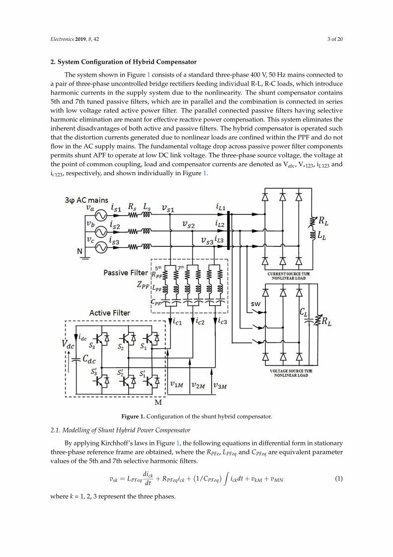
The system shown in Figure 1 consists of a standard three-phase 400 V, 50 Hz mains connected toa pair of three-phase uncontrolled bridge rectifiers feeding individual R-L, R-C loads, which introduceharmonic currents in the supply system due to the nonlinearity. The shunt compensator contains5th and 7th tuned passive filters, which are in parallel and the combination is connected in serieswith low voltage rated active power filter. The parallel connected passive filters having selectiveharmonic elimination are meant for effective reactive power compensation. This system eliminates theinherent disadvantages of both active and passive filters. The hybrid compensator is operated suchthat the distortion currents generated due to nonlinear loads are confined within the PPF and do notflow in the AC supply mains. The fundamental voltage drop across passive power filter componentspermits shunt APF to operate at low DC link voltage. The three-phase source voltage, the voltage atthe point of common coupling, load and compensator currents are denoted as Vabc, Vs123, iL123 andic123, respectively, and shown individually in Figure 1.
Electronics 2019, 8, x FOR PEER REVIEW 3 of 20
2. System Configuration of Hybrid Compensator
The system shown in Figure 1 consists of a standard three-phase 400 V, 50 Hz mains connected to a pair of three-phase uncontrolled bridge rectifiers feeding individual R-L, R-C loads, which introduce harmonic currents in the supply system due to the nonlinearity. The shunt compensator contains 5th and 7th tuned passive filters, which are in parallel and the combination is connected in series with low voltage rated active power filter. The parallel connected passive filters having selective harmonic elimination are meant for effective reactive power compensation. This system eliminates the inherent disadvantages of both active and passive filters. The hybrid compensator is operated such that the distortion currents generated due to nonlinear loads are confined within the PPF and do not flow in the AC supply mains. The fundamental voltage drop across passive power filter components permits shunt APF to operate at low DC link voltage. The three-phase source voltage, the voltage at the point of common coupling, load and compensator currents are denoted as Vabc, Vs123, iL123 and ic123, respectively, and shown individually in Figure 1.
Figure 1. Configuration of the shunt hybrid compensator.
2.1. Modelling of Shunt Hybrid Power Compensator
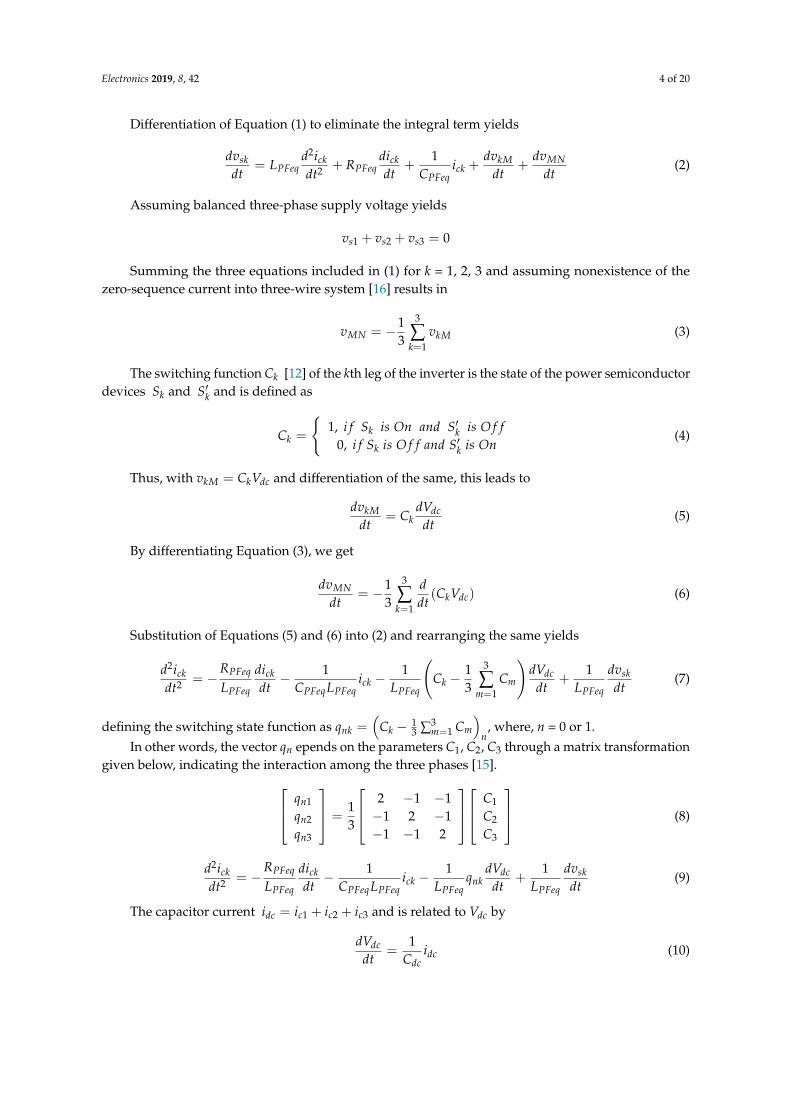
By applying Kirchhoff’s laws in Figure 1, the following equations in differential form in stationary three-phase reference frame are obtained, where the RPFe, LPFeq and CPFeq are equivalent parameter values of the 5th and 7th selective harmonic filters. 𝑣 = 𝐿 𝑑𝑖𝑑𝑡 + 𝑅 𝑖 + 1 𝐶⁄ 𝑖 𝑑𝑡 + 𝑣 + 𝑣 (1)
where k = 1, 2, 3 represent the three phases. Differentiation of Equation (1) to eliminate the integral term yields
Figure 1. Configuration of the shunt hybrid compensator.
2.1. Modelling of Shunt Hybrid Power Compensator
By applying Kirchhoff’s laws in Figure 1, the following equations in differential form in stationarythree-phase reference frame are obtained, where the RPFe, LPFeq and CPFeq are equivalent parametervalues of the 5th and 7th selective harmonic filters.
vsk = LPFeqdickdt
+ RPFeqick +(1/CPFeq
) ∫ickdt + vkM + vMN (1)
where k = 1, 2, 3 represent the three phases.
Electronics 2019, 8, 42 4 of 20
Differentiation of Equation (1) to eliminate the integral term yields
dvskdt
= LPFeqd2ickdt2 + RPFeq
dickdt
+1
CPFeqick +
dvkMdt
+dvMN
dt(2)
Assuming balanced three-phase supply voltage yields
vs1 + vs2 + vs3 = 0
Summing the three equations included in (1) for k = 1, 2, 3 and assuming nonexistence of thezero-sequence current into three-wire system [16] results in
vMN = −13
3
∑k=1
vkM (3)
The switching function Ck [12] of the kth leg of the inverter is the state of the power semiconductordevices Sk and S′k and is defined as
Ck =
1, i f Sk is On and S′k is O f f
0, i f Sk is O f f and S′k is On(4)
Thus, with vkM = CkVdc and differentiation of the same, this leads to
dvkMdt
= CkdVdc
dt(5)
By differentiating Equation (3), we get
dvMNdt
= −13
3
∑k=1
ddt(CkVdc) (6)
Substitution of Equations (5) and (6) into (2) and rearranging the same yields
d2ickdt2 = −
RPFeq
LPFeq
dickdt− 1
CPFeqLPFeqick −
1LPFeq
(Ck −
13
3
∑m=1
Cm
)dVdc
dt+
1LPFeq
dvskdt
(7)
defining the switching state function as qnk =(
Ck − 13 ∑3
m=1 Cm
)n, where, n = 0 or 1.
In other words, the vector qn epends on the parameters C1, C2, C3 through a matrix transformationgiven below, indicating the interaction among the three phases [15]. qn1
qn2
qn3
=13
2 −1 −1−1 2 −1−1 −1 2
C1
C2
C3
(8)
d2ickdt2 = −
RPFeq
LPFeq
dickdt− 1
CPFeqLPFeqick −
1LPFeq
qnkdVdc
dt+
1LPFeq
dvskdt
(9)
The capacitor current idc = ic1 + ic2 + ic3 and is related to Vdc by
dVdcdt
=1
Cdcidc (10)
Electronics 2019, 8, 42 5 of 20
Expressing the DClink capacitor current idc in terms of the switching and compensator currents,the following equation is obtained
dVdcdt
=1
Cdc
3
∑k=1
qnkick =1
Cdc[qn123]
T [ic123] (11)
In the nonexistence of zero-sequence currents, the variables ic3 and qn3 can be eliminated by thesubstitution of ic3 = −(ic1 + ic2) and qn3 = −(qn1 + qn2) so that Equation (11) for the modelling of thecapacitor is modified as follows.
dVdcdt
=1
Cdc[2qn1 + qn2]ic1 +
1Cdc
[qn1 + 2qn2]ic2 (12)
The complete model of the shunt hybrid power compensator in abc reference frame is indicatedby Equations (9) and (12).
2.2. Equations in dq Frame
The model given by Equations (9) and (12) is transformed into synchronous orthogonal frameusing the transformation matrix [13]
T123dq =
√23
cosθ cos(θ − 2π
3)
cos(
θ − 4π3
)−sinθ −sin
(θ − 2π
3)−sin
(θ − 4π
3
) (13)
where θ = ωt and ω represents the mains frequency.
Since T123dq is orthogonal,
(T123
dq
)−1=(
T123dq
)Tand Equation (12) can be written as
dVdcdt
=1
Cdc
(T123
dq
[qndq
])T(T123
dq
[idq
])=
1Cdc
[qndq
][idq
](14)
On the other hand, Equation (9) can be written as
d2
dt2 [ic12] = −RPFeq
LPFeq
ddt[ic12]−
1CPFeqLPFeq
[ic12]−1
LPFeq[qn12]
dVdcdt
+1
LPFeq
ddt[vs12] (15)
The three-phase current with the absence of zero-sequence components can be converted intod-q frame using reduced transformation matrix. Applying the transformations in Equation (15),the complete d-q frame dynamic model of the system is obtained as follows;
LPFeqd2iddt2 = −RPFeq
diddt + 2ωLPFeq
diqdt −
(−ω2LPFeq +
1CPFeq
)id + ωRPFeqiq − qnd
dVdcdt + dvd
dt −ωvq (16)
LPFeqd2iqdt2 = −RPFeq
diqdt − 2ωLPFeq
diddt −
(−ω2LPFeq +
1CPFeq
)iq −ωRPFeqid − qnq
dVdcdt +
dvqdt + ωvd (17)
CdcdVdc
dt= qndid + qnqiq (18)
The role of id in Equation (16) is interpreted as the component for meeting the switching lossesin the compensator, whereas the component iq is utilised to supply reactive power and maintain theDClink voltage across the capacitor for sustaining the compensator action.
It is specifically noted that this set of Equations (16)–(18) contain nonlinear terms involving thecontrol variables qnd and qnq. Accordingly, the implementation of this control strategy is termed asnonlinear control technique by many authors in the literature [12,15,16].
Electronics 2019, 8, 42 6 of 20
2.3. Control of Harmonic Currents
Based on the load and compensator models presented in Section 2.2, the control problem isformulated with the objective of minimizing supply-side current harmonics and improving the powerfactor. Also, for maintaining the performance during load fluctuations, it is necessary to maintain adesired DC link capacitor voltage. The control law is derived using the following approach.
Rewriting Equations (16) and (17) in a more convenient form, we get
LPFeqd2iddt2 + RPFeq
diddt +
(−ω2LPFeq +
1CPFeq
)id
= 2ωLPFeqdiqdt + ωRPFeqiq − qnd
dVdcdt + dvd
dt −ωvq
(19)
LPFeqd2iqdt2 + RPFeq
diqdt +
(−ω2LPFeq +
1CPFeq
)iq
= −2ωLPFeqdiqdt −ωRPFeqid − qnq
dVdcdt +
dvqdt + ωvd
(20)
The control variables ud and uq are defined as
ud = 2ωLPFeqdiqdt
+ ωRPFeqiq − qnddVdc
dt+
dvddt−ωvq (21)
uq = −2ωLPFeqdiddt−ωRPFeqid − qnq
dVdcdt
+dVq
dt+ ωvd (22)
Using the idea of decoupling the current harmonic components for the purpose of tracking thereference current, the error signals id = i∗d − id and iq = i∗q − iq are generated and processed through apair of PI controllers [12,14] to obtain ud and uq signals which are given below.
i∗d and i∗q are the reference currents deduced from the load current, id and iq are the actualcompensator currents.Load current in d-q coordinate is processed using a pair of fourth-orderButterworth low-pass filters with cut-off frequency set at 60 Hz to extract the harmonic currentreferences alone.
ud = KPid + KI
∫iddt
uq = KPiq + KI
∫iqdt
From Equations (19) and (20), we obtain the transfer function as follows
Id(s)Ud(s)
=Iq(s)
Uq(s)=
1
LPFeq
(s2 +
RPFeqLPFeq
s + 1CPFeq LPFeq
−ω2) (23)
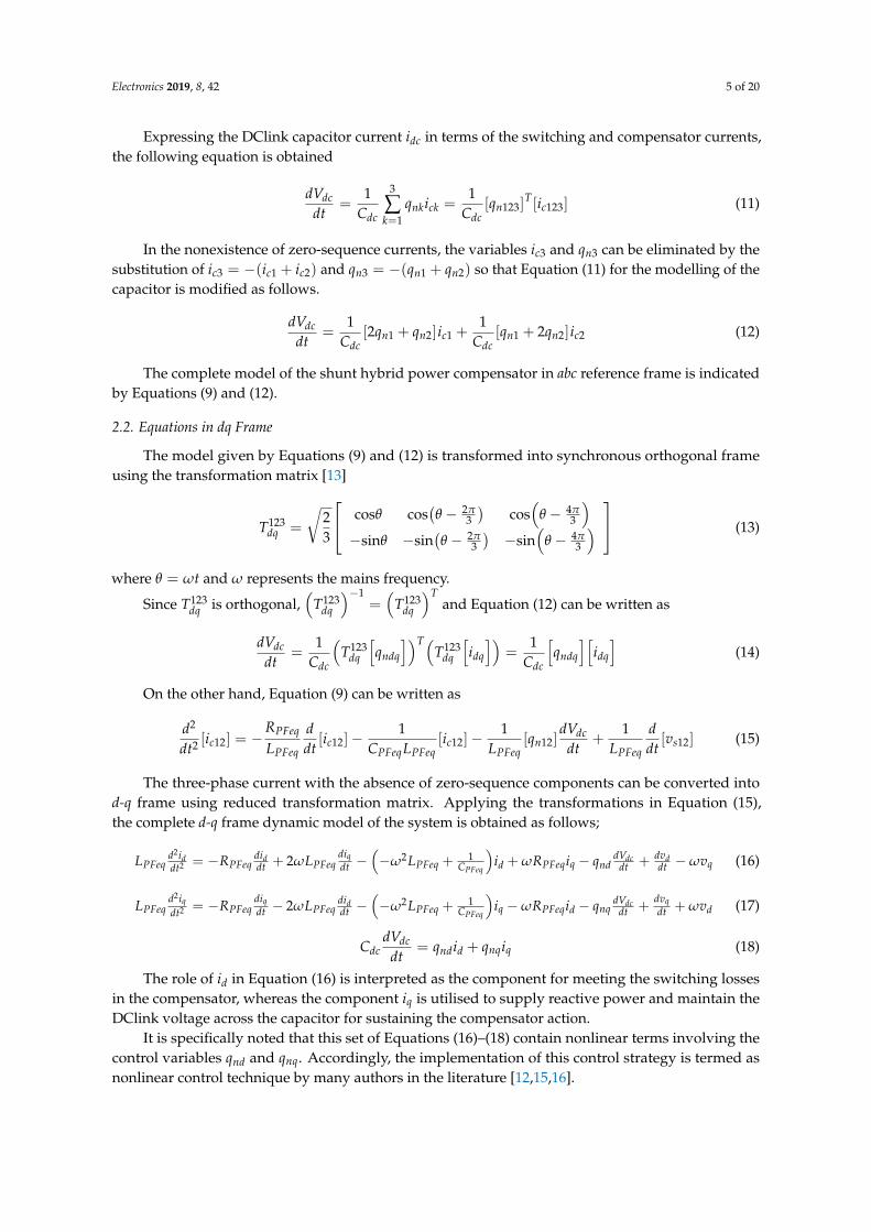
The current control of the closed-loop system is shown in Figure 2 and represents the signalflow of the variables iq(s); the other component id(s) is obtained concurrently in a similar manner.The transfer function of the full closed-loop control module is derived as
The control variables 𝑢 and 𝑢 are defined as 𝑢 = 2𝜔𝐿 𝑑𝑖𝑑𝑡 + 𝜔𝑅 𝑖 − 𝑞 𝑑𝑉𝑑𝑡 + 𝑑𝑣𝑑𝑡 − 𝜔𝑣 (21)
𝑢 = −2𝜔𝐿 𝑑𝑖𝑑𝑡 − 𝜔𝑅 𝑖 − 𝑞 𝑑𝑉𝑑𝑡 + 𝑑𝑉𝑑𝑡 + 𝜔𝑣 (22)
Using the idea of decoupling the current harmonic components for the purpose of tracking the reference current, the error signals 𝚤 = 𝑖∗ − 𝑖 and 𝚤 = 𝑖∗ − 𝑖 are generated and processed through a pair of PI controllers [12,14] to obtain 𝑢 and 𝑢 signals which are given below. 𝑖∗ and 𝑖∗ are the reference currents deduced from the load current, 𝑖 and 𝑖 are the actual compensator currents.Load current in d-q coordinate is processed using a pair of fourth-order Butterworth low-pass filters with cut-off frequency set at 60 Hz to extract the harmonic current references alone. 𝑢 = 𝐾 𝚤 + 𝐾 𝚤 𝑑𝑡 𝑢 = 𝐾 𝚤 + 𝐾 𝚤 𝑑𝑡
From Equations (19) and (20), we obtain the transfer function as follows 𝐼 (𝑠)𝑈 (𝑠) = 𝐼 (𝑠)𝑈 (𝑠) = 1𝐿 𝑠 + 𝑅𝐿 𝑠 + 1𝐶 𝐿 − 𝜔 (23)
The current control of the closed-loop system is shown in Figure 2 and represents the signal flow of the variables 𝑖 (𝑠); the other component 𝑖 (𝑠) is obtained concurrently in a similar manner. The transfer function of the full closed-loop control module is derived as 𝐼 (𝑠)𝐼∗(𝑠) = 𝐾𝐿 ⎣⎢⎢
Figure 2. Structure of current control loop for iq and id.
From Equations (21) and (22), the control variables of the proposed system are defined by the following equations.
Figure 2. Structure of current control loop for iq and id.
Electronics 2019, 8, 42 7 of 20
From Equations (21) and (22), the control variables of the proposed system are defined by thefollowing equations.
qnd =2ωLPFeq
diqdt + ωRPFeqiq +
dVddt −ωvq − ud
dVdcdt
(25)
qnq =−2ωLPFeq
diddt + ωRPFeqid +
dVqdt −ωvd − uq
dVdcdt
(26)
The above equations represent both the decoupled linear compensation part and cancellationof nonlinearity.
2.4. DC Link Voltage Control
The capacitor in the APF does not need any external DC source but gets charged through therectifier action of the built-in reverse diodes across the six Insulated-gate bipolar transistors (IGBTs).The power loss in the capacitor and switching losses in the inverter have to be met by the activecomponent id of the compensator current from the mains, while the component iq supplies the reactivepower stored in the capacitor. The power losses in this circuit can reduce the DC link capacitor voltage,thereby weakening the function of the active filter. Hence, it is necessary to maintain the voltageacross the DC link capacitor at a designed reference value by an additional voltage regulator, whichmodifies the PWM signals appropriately. This regulator is implemented by using a PI controller [12],which processes the error between the reference voltage V∗dc and the actual capacitor voltage Vdc.The parameters of the PI regulator are chosen in such a way that the DC voltage is maintained aroundits desired value. The design values for the PI controller parameters have been obtained following theapproach suggested by Salem Rahmani et al. [13,14]. The overall transfer function of this controller isincorporated as a subsystem in the simulation schematic.
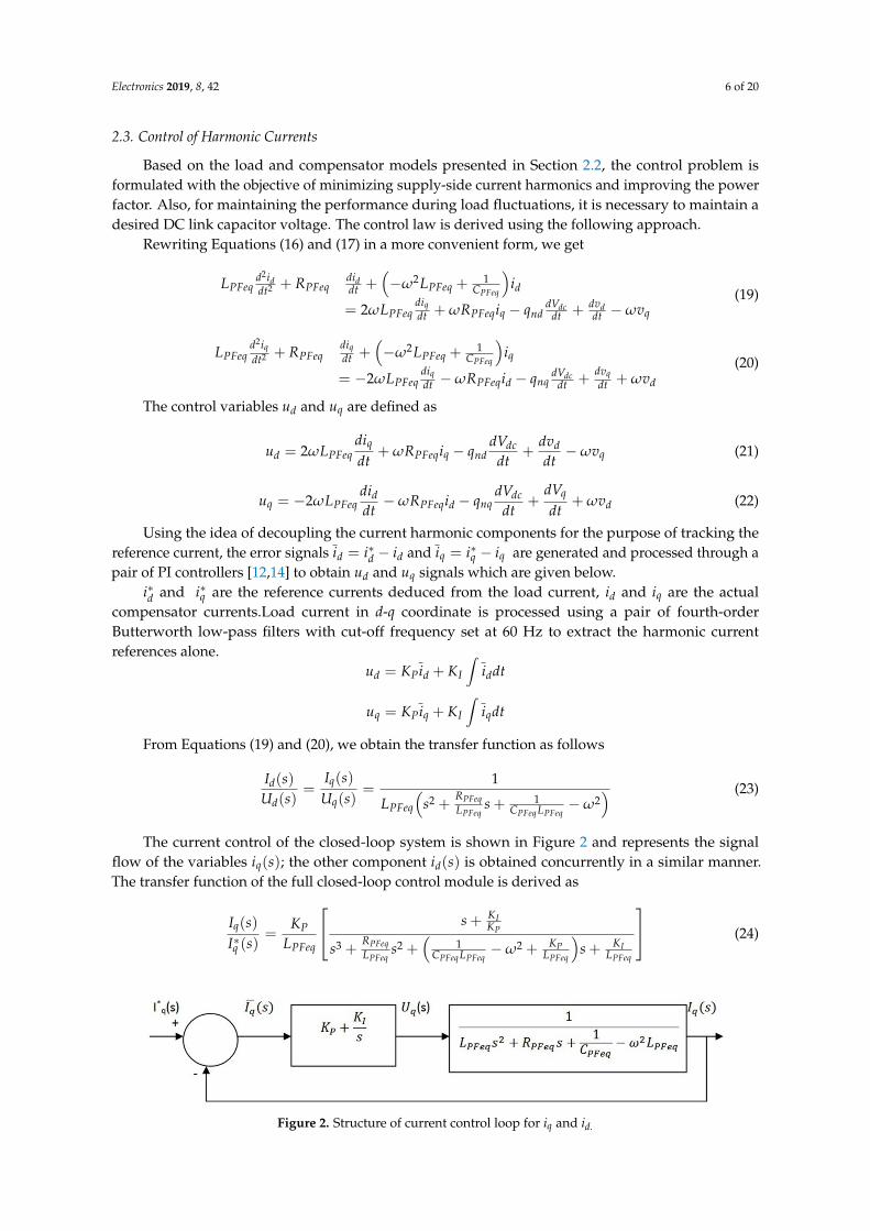
The control scheme of the proposed hybrid power compensator is shown in Figure 3, where thevarious signals such as Vdc, V∗dc, id, iq, i∗d and i∗q are processed using Equations (21) to (26) to obtain thegate trigger signals.
Electronics 2019, 8, x FOR PEER REVIEW 7 of 20
𝑞 = 2𝜔𝐿 𝑑𝑖𝑑𝑡 + 𝜔𝑅 𝑖 + 𝑑𝑉𝑑𝑡 − 𝜔𝑣 − 𝑢𝑑𝑉𝑑𝑡 (25)
𝑞 = −2𝜔𝐿 𝑑𝑖𝑑𝑡 + 𝜔𝑅 𝑖 + 𝑑𝑉𝑑𝑡 − 𝜔𝑣 − 𝑢𝑑𝑉𝑑𝑡 (26)
The above equations represent both the decoupled linear compensation part and cancellation of nonlinearity.
2.4. DC Link Voltage Control
The capacitor in the APF does not need any external DC source but gets charged through the rectifier action of the built-in reverse diodes across the six Insulated-gate bipolar transistors (IGBTs). The power loss in the capacitor and switching losses in the inverter have to be met by the active component id of the compensator current from the mains, while the component iq supplies the reactive power stored in the capacitor. The power losses in this circuit can reduce the DC link capacitor voltage, thereby weakening the function of the active filter. Hence, it is necessary to maintain the voltage across the DC link capacitor at a designed reference value by an additional voltage regulator, which modifies the PWM signals appropriately. This regulator is implemented by using a PI controller [12], which processes the error between the reference voltage 𝑉∗ and the actual capacitor voltage Vdc. The parameters of the PI regulator are chosen in such a way that the DC voltage is maintained around its desired value. The design values for the PI controller parameters have been obtained following the approach suggested by Salem Rahmani et al. [13,14]. The overall transfer function of this controller is incorporated as a subsystem in the simulation schematic.
The control scheme of the proposed hybrid power compensator is shown in Figure 3, where the various signals such as Vdc, 𝑉∗ , 𝑖 , 𝑖 , 𝑖∗ and 𝑖∗ are processed using Equations (21) to (26) to obtain the gate trigger signals.
Figure 3. Control structure of the shunt hybrid compensator.
2.5. Simulink Model of the Shunt Hybrid Power Compensator
The Simulink schematic of the power distribution system along with the proposed shunt hybrid power compensator, which translates the entire system equations presented in Section 2 into functional blocks in the Simulink model, has been developed using MATLAB software. The nonlinear load has been modelled using a three-phase full bridge diode rectifier feeding RL and RC loads separately as subsystems and connected to the three phase mains. At the source side, a resistor–inductor combination is used to represent the line impedance of each phase before PCC. The
Figure 3. Control structure of the shunt hybrid compensator.
2.5. Simulink Model of the Shunt Hybrid Power Compensator
The Simulink schematic of the power distribution system along with the proposed shunt hybridpower compensator, which translates the entire system equations presented in Section 2 into functionalblocks in the Simulink model, has been developed using MATLAB software. The nonlinear load hasbeen modelled using a three-phase full bridge diode rectifier feeding RL and RC loads separately as
Electronics 2019, 8, 42 8 of 20
subsystems and connected to the three phase mains. At the source side, a resistor–inductor combinationis used to represent the line impedance of each phase before PCC. The unbalance case in the nonlinearload has been formed by connecting a single-phase diode rectifier feeding RL load between phase1 andground. The synchronization of the subsystem with main supply frequency is accomplished by usinga three-phase discrete PLL block [22–25]. The PLL block detects the supply frequency; the detectedsupply frequency is used to synchronize the compensator d-q axis current and the distorted loadd-q axis current to extract harmonic component needs to be compensated. During load disturbanceand supply voltage distortions, the variation in the supply frequency is detected by the PLL block andsynchronizes the subsystems accordingly.
The hybrid filter consists of a parallel connection of selective 5th and 7th harmonic eliminationpassive filters as depicted in Figure 1 along with APF. The entire system simulation is carried out in adiscrete mode, variable step size with ode45 (Dormand–Prince) solver.
3. Simulation Results
To evaluate the performance of the shunt HPF controlled by the proposed control algorithm, aSimulink-based schematic was created so as to operate from a 400 V, 50 Hz supply. The load consistsof a set of balanced and unbalanced nonlinear loads, which are selectively connected for successivesimulation runs. In this work, the performances of the compensator corresponding to the followingloads are analysed: (i) three-phase rectifier feeding RL load, (ii) three-phase rectifier feeding RC load,(iii) dynamic load variation and (iv) unbalanced load. Table 1 indicates the specification of the systemparameters used in the simulation.
Table 1. Parameters of the system.
Phase Voltage and Frequency Vsrms = 230 V and fs = 50 Hz
Impedance of the line Rs = 0.1 Ω, Ls = 4 mHNonlinear load of current source type RL = 50 Ω, LL = 10 mHNonlinear load of voltage source type
5th tuned PPF parameters7th tuned PPF parameters
RL = 32 Ω, CL = 1000 µFR = 0.1 Ω, L = 10 mH, C = 40 µFR = 0.1 Ω, L = 7 mH, C = 30 µF
DClink voltage and capacitance Vdc = 25 V, Cdc = 6600 µFParameters of the outer loop PI controller k1 = 0.22 and k2 = 15.85
Inner loop PI controller parameters KP = 0.6 and KI = 1.2
3.1. Performance of Shunt HPF to the Nonlinear Load of Current Source Type
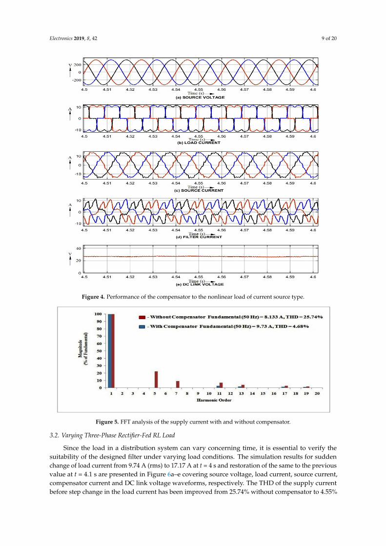
The three-phase mains supply a diode bridge rectifier, whose output is wired to a balancedR-L load, which imposes a typical nonlinearity, resulting in harmonic currents at the supply end.The proposed hybrid shunt compensator is wired at PCC as shown in Figure 1. The results are shownin Figure 4a–e covering the waveforms of the supply voltage, currents of the load, source current aftercompensation, currents of the compensator and DC link voltage, respectively. The waveform depictsthat the supply current waveform is almost sinusoidal after compensation and the DC link capacitorvoltage is maintained constant. Figure 5 depicts the simulation results covering the harmonic spectrumof the supply current before and after compensation. The results indicate that the THD of the supplycurrent is reduced from 25.74% without compensator to 4.68% with compensator. It is seen that theproposed control strategy with shunt HPF can mitigate the current harmonics present in the supplysystem within the limit specified by IEEE 519-1992 standards.
Electronics 2019, 8, 42 9 of 20Electronics 2019, 8, x FOR PEER REVIEW 9 of 20
Figure 4. Performance of the compensator to the nonlinear load of current source type.
Figure 5. FFT analysis of the supply current with and without compensator.
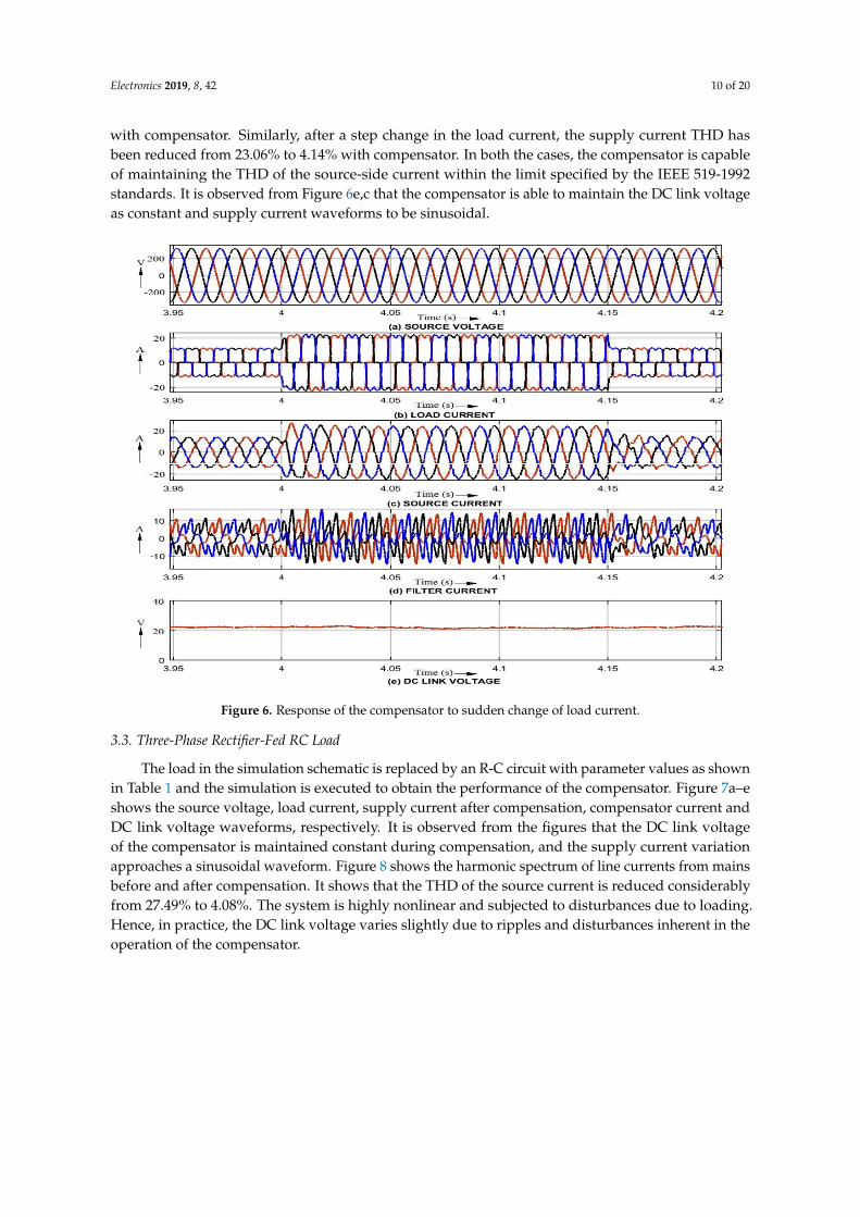
3.2. Varying Three-Phase Rectifier-Fed RL Load
Since the load in a distribution system can vary concerning time, it is essential to verify the suitability of the designed filter under varying load conditions. The simulation results for sudden change of load current from 9.74 A (rms) to 17.17 A at t = 4 s and restoration of the same to the previous value at t = 4.1 s are presented in Figure 6a–e covering source voltage, load current, source current, compensator current and DC link voltage waveforms, respectively. The THD of the supply current before step change in the load current has been improved from 25.74% without compensator to 4.55% with compensator. Similarly, after a step change in the load current, the supply current THD has been reduced from 23.06% to 4.14% with compensator. In both the cases, the compensator is
Figure 4. Performance of the compensator to the nonlinear load of current source type.
Electronics 2019, 8, x FOR PEER REVIEW 9 of 20
Figure 4. Performance of the compensator to the nonlinear load of current source type.
Figure 5. FFT analysis of the supply current with and without compensator.
3.2. Varying Three-Phase Rectifier-Fed RL Load
Since the load in a distribution system can vary concerning time, it is essential to verify the suitability of the designed filter under varying load conditions. The simulation results for sudden change of load current from 9.74 A (rms) to 17.17 A at t = 4 s and restoration of the same to the previous value at t = 4.1 s are presented in Figure 6a–e covering source voltage, load current, source current, compensator current and DC link voltage waveforms, respectively. The THD of the supply current before step change in the load current has been improved from 25.74% without compensator to 4.55% with compensator. Similarly, after a step change in the load current, the supply current THD has been reduced from 23.06% to 4.14% with compensator. In both the cases, the compensator is
Figure 5. FFT analysis of the supply current with and without compensator.
3.2. Varying Three-Phase Rectifier-Fed RL Load
Since the load in a distribution system can vary concerning time, it is essential to verify thesuitability of the designed filter under varying load conditions. The simulation results for suddenchange of load current from 9.74 A (rms) to 17.17 A at t = 4 s and restoration of the same to the previousvalue at t = 4.1 s are presented in Figure 6a–e covering source voltage, load current, source current,compensator current and DC link voltage waveforms, respectively. The THD of the supply currentbefore step change in the load current has been improved from 25.74% without compensator to 4.55%
Electronics 2019, 8, 42 10 of 20
with compensator. Similarly, after a step change in the load current, the supply current THD hasbeen reduced from 23.06% to 4.14% with compensator. In both the cases, the compensator is capableof maintaining the THD of the source-side current within the limit specified by the IEEE 519-1992standards. It is observed from Figure 6e,c that the compensator is able to maintain the DC link voltageas constant and supply current waveforms to be sinusoidal.
Electronics 2019, 8, x FOR PEER REVIEW 10 of 20
capable of maintaining the THD of the source-side current within the limit specified by the IEEE 519-1992 standards. It is observed from Figure 6e and c that the compensator is able to maintain the DC link voltage as constant and supply current waveforms to be sinusoidal.
Figure 6. Response of the compensator to sudden change of load current.
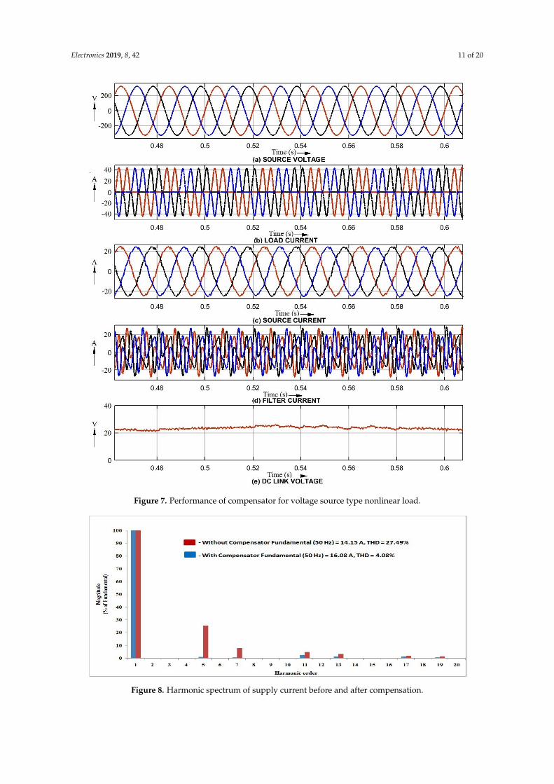
3.3. Three-Phase Rectifier-Fed RC Load
The load in the simulation schematic is replaced by an R-C circuit with parameter values as shown in Table 1 and the simulation is executed to obtain the performance of the compensator. Figure 7a–e shows the source voltage, load current, supply current after compensation, compensator current and DC link voltage waveforms, respectively. It is observed from the figures that the DC link voltage of the compensator is maintained constant during compensation, and the supply current variation approaches a sinusoidal waveform. Figure 8 shows the harmonic spectrum of line currents from mains before and after compensation. It shows that the THD of the source current is reduced considerably from 27.49% to 4.08%. The system is highly nonlinear and subjected to disturbances due to loading. Hence, in practice, the DC link voltage varies slightly due to ripples and disturbances inherent in the operation of the compensator.
Figure 6. Response of the compensator to sudden change of load current.
3.3. Three-Phase Rectifier-Fed RC Load
The load in the simulation schematic is replaced by an R-C circuit with parameter values as shownin Table 1 and the simulation is executed to obtain the performance of the compensator. Figure 7a–eshows the source voltage, load current, supply current after compensation, compensator current andDC link voltage waveforms, respectively. It is observed from the figures that the DC link voltageof the compensator is maintained constant during compensation, and the supply current variationapproaches a sinusoidal waveform. Figure 8 shows the harmonic spectrum of line currents from mainsbefore and after compensation. It shows that the THD of the source current is reduced considerablyfrom 27.49% to 4.08%. The system is highly nonlinear and subjected to disturbances due to loading.Hence, in practice, the DC link voltage varies slightly due to ripples and disturbances inherent in theoperation of the compensator.
Electronics 2019, 8, 42 11 of 20Electronics 2019, 8, x FOR PEER REVIEW 11 of 20
Figure 7. Performance of compensator for voltage source type nonlinear load.
Figure 8. Harmonic spectrum of supply current before and after compensation.
Figure 7. Performance of compensator for voltage source type nonlinear load.
Electronics 2019, 8, x FOR PEER REVIEW 11 of 20
Figure 7. Performance of compensator for voltage source type nonlinear load.
Figure 8. Harmonic spectrum of supply current before and after compensation.
Figure 8. Harmonic spectrum of supply current before and after compensation.
Electronics 2019, 8, 42 12 of 20
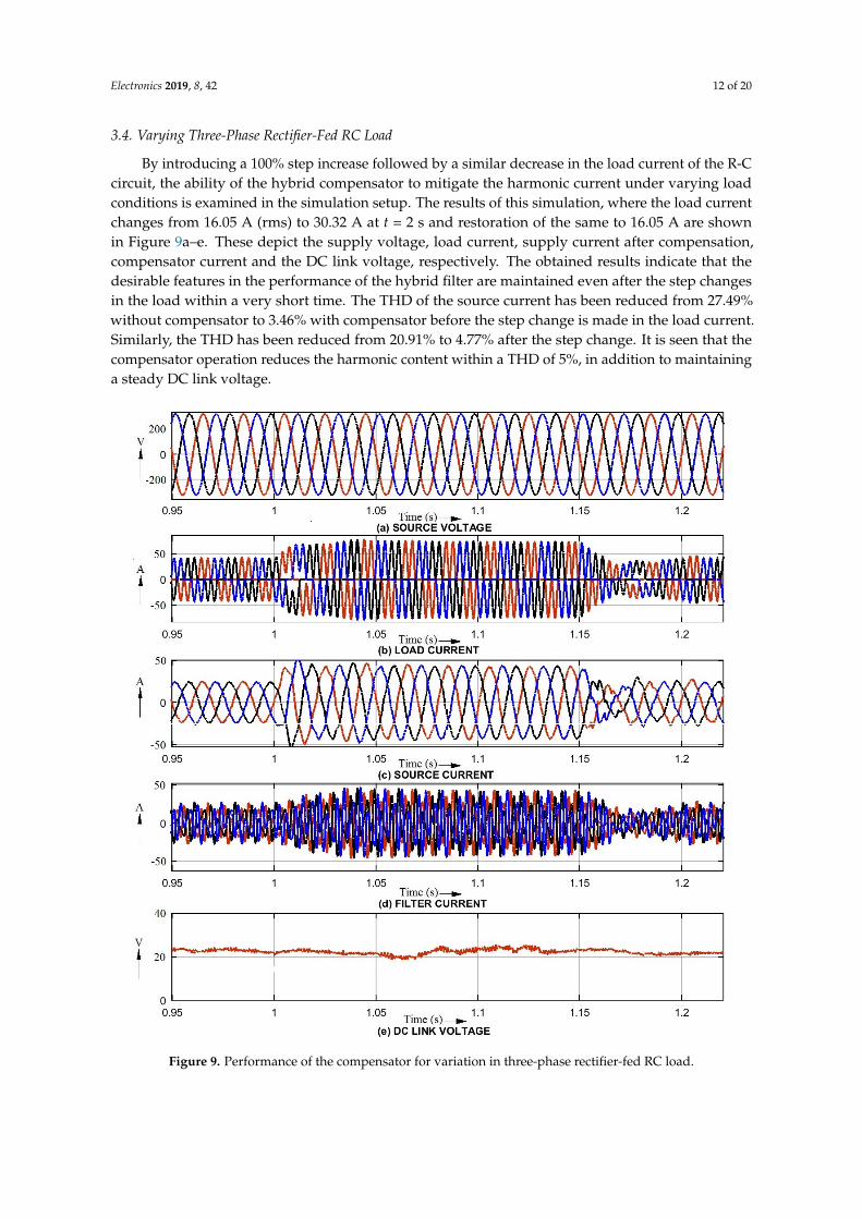
3.4. Varying Three-Phase Rectifier-Fed RC Load
By introducing a 100% step increase followed by a similar decrease in the load current of the R-Ccircuit, the ability of the hybrid compensator to mitigate the harmonic current under varying loadconditions is examined in the simulation setup. The results of this simulation, where the load currentchanges from 16.05 A (rms) to 30.32 A at t = 2 s and restoration of the same to 16.05 A are shownin Figure 9a–e. These depict the supply voltage, load current, supply current after compensation,compensator current and the DC link voltage, respectively. The obtained results indicate that thedesirable features in the performance of the hybrid filter are maintained even after the step changesin the load within a very short time. The THD of the source current has been reduced from 27.49%without compensator to 3.46% with compensator before the step change is made in the load current.Similarly, the THD has been reduced from 20.91% to 4.77% after the step change. It is seen that thecompensator operation reduces the harmonic content within a THD of 5%, in addition to maintaininga steady DC link voltage.
Electronics 2019, 8, x FOR PEER REVIEW 12 of 20
3.4. Varying Three-Phase Rectifier-Fed RC Load
By introducing a 100% step increase followed by a similar decrease in the load current of the R-C circuit, the ability of the hybrid compensator to mitigate the harmonic current under varying load conditions is examined in the simulation setup. The results of this simulation, where the load current changes from 16.05 A (rms) to 30.32 A at t = 2 s and restoration of the same to 16.05 A are shown in Figure 9a–e. These depict the supply voltage, load current, supply current after compensation, compensator current and the DC link voltage, respectively. The obtained results indicate that the desirable features in the performance of the hybrid filter are maintained even after the step changes in the load within a very short time. The THD of the source current has been reduced from 27.49% without compensator to 3.46% with compensator before the step change is made in the load current. Similarly, the THD has been reduced from 20.91% to 4.77% after the step change. It is seen that the compensator operation reduces the harmonic content within a THD of 5%, in addition to maintaining a steady DC link voltage.
Figure 9. Performance of the compensator for variation in three-phase rectifier-fed RC load.
Figure 9. Performance of the compensator for variation in three-phase rectifier-fed RC load.
Electronics 2019, 8, 42 13 of 20
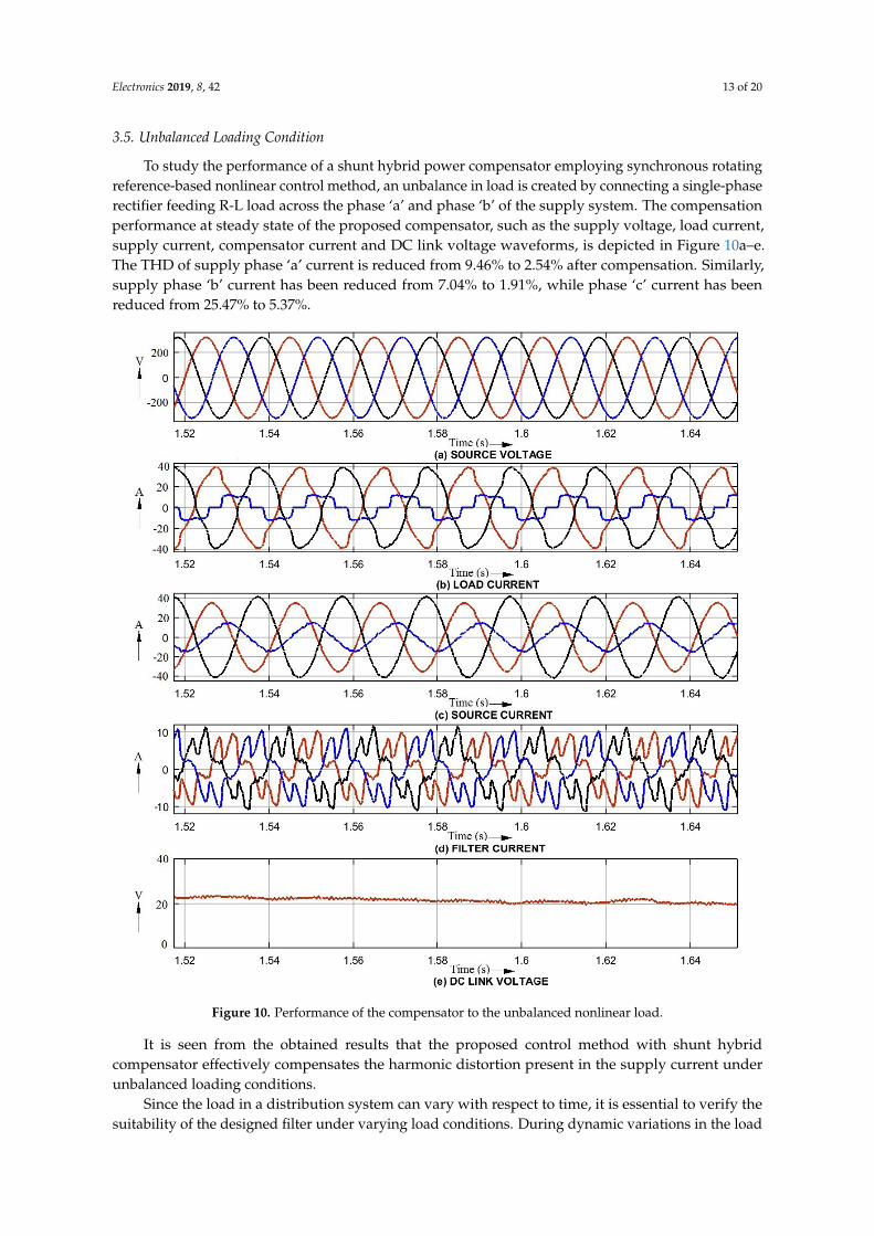
3.5. Unbalanced Loading Condition
To study the performance of a shunt hybrid power compensator employing synchronous rotatingreference-based nonlinear control method, an unbalance in load is created by connecting a single-phaserectifier feeding R-L load across the phase ‘a’ and phase ‘b’ of the supply system. The compensationperformance at steady state of the proposed compensator, such as the supply voltage, load current,supply current, compensator current and DC link voltage waveforms, is depicted in Figure 10a–e.The THD of supply phase ‘a’ current is reduced from 9.46% to 2.54% after compensation. Similarly,supply phase ‘b’ current has been reduced from 7.04% to 1.91%, while phase ‘c’ current has beenreduced from 25.47% to 5.37%.
Electronics 2019, 8, x FOR PEER REVIEW 13 of 20
3.5. Unbalanced Loading Condition
To study the performance of a shunt hybrid power compensator employing synchronous rotating reference-based nonlinear control method, an unbalance in load is created by connecting a single-phase rectifier feeding R-L load across the phase ‘a’ and phase ‘b’ of the supply system. The compensation performance at steady state of the proposed compensator, such as the supply voltage, load current, supply current, compensator current and DC link voltage waveforms, is depicted in Figure 10a–e. The THD of supply phase ‘a’ current is reduced from 9.46% to 2.54% after compensation. Similarly, supply phase ‘b’ current has been reduced from 7.04% to 1.91%, while phase ‘c’ current has been reduced from 25.47% to 5.37%.
Figure 10. Performance of the compensator to the unbalanced nonlinear load.
It is seen from the obtained results that the proposed control method with shunt hybrid compensator effectively compensates the harmonic distortion present in the supply current under unbalanced loading conditions.
Since the load in a distribution system can vary with respect to time, it is essential to verify the suitability of the designed filter under varying load conditions. During dynamic variations in the
Figure 10. Performance of the compensator to the unbalanced nonlinear load.
It is seen from the obtained results that the proposed control method with shunt hybridcompensator effectively compensates the harmonic distortion present in the supply current underunbalanced loading conditions.
Since the load in a distribution system can vary with respect to time, it is essential to verify thesuitability of the designed filter under varying load conditions. During dynamic variations in the load
Electronics 2019, 8, 42 14 of 20
current and unbalance, as shown in Figures 6, 9 and 10, the compensator is able to maintain constantDC link voltage as well as reduce the amount of harmonics present in the system.
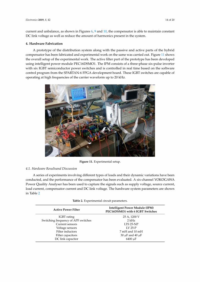
4. Hardware Fabrication
A prototype of the distribution system along with the passive and active parts of the hybridcompensator has been fabricated and experimental work on the same was carried out. Figure 11 showsthe overall setup of the experimental work. The active filter part of the prototype has been developedusing intelligent power module PEC16DSMO1. The IPM consists of a three-phase six-pulse inverterwith six IGBT semiconductor power switches and is controlled in real time based on the softwarecontrol program from the SPARTAN-6 FPGA development board. These IGBT switches are capable ofoperating at high frequencies of the carrier waveform up to 20 kHz.
Electronics 2019, 8, x FOR PEER REVIEW 14 of 20
load current and unbalance, as shown in Figures 6, 9 and 10, the compensator is able to maintain constant DC link voltage as well as reduce the amount of harmonics present in the system.
4. Hardware Fabrication
A prototype of the distribution system along with the passive and active parts of the hybrid compensator has been fabricated and experimental work on the same was carried out. Figure 11 shows the overall setup of the experimental work. The active filter part of the prototype has been developed using intelligent power module PEC16DSMO1. The IPM consists of a three-phase six-pulse inverter with six IGBT semiconductor power switches and is controlled in real time based on the software control program from the SPARTAN-6 FPGA development board. These IGBT switches are capable of operating at high frequencies of the carrier waveform up to 20 kHz.
Figure 11. Experimental setup.
4.1. Hardware Resultsand Discussion
A series of experiments involving different types of loads and their dynamic variations have been conducted, and the performance of the compensator has been evaluated. A six-channel YOKOGAWA Power Quality Analyser has been used to capture the signals such as supply voltage, source current, load current, compensator current and DC link voltage. The hardware system parameters are shown in Table 2
Table 2. Experimental circuit parameters.
Active Power Filter Intelligent Power Module (IPM) PEC16DSMO1 with 6 IGBT Switches IGBT rating 25 A, 1200 V
Switching frequency of APF switches 2 kHz Current sensors LTS 25-NP Voltage sensors LV 25-P Filter inductors 7 mH and 10 mH Filter capacitors 30 µF and 40 µF
DC link capacitor 6400 µF
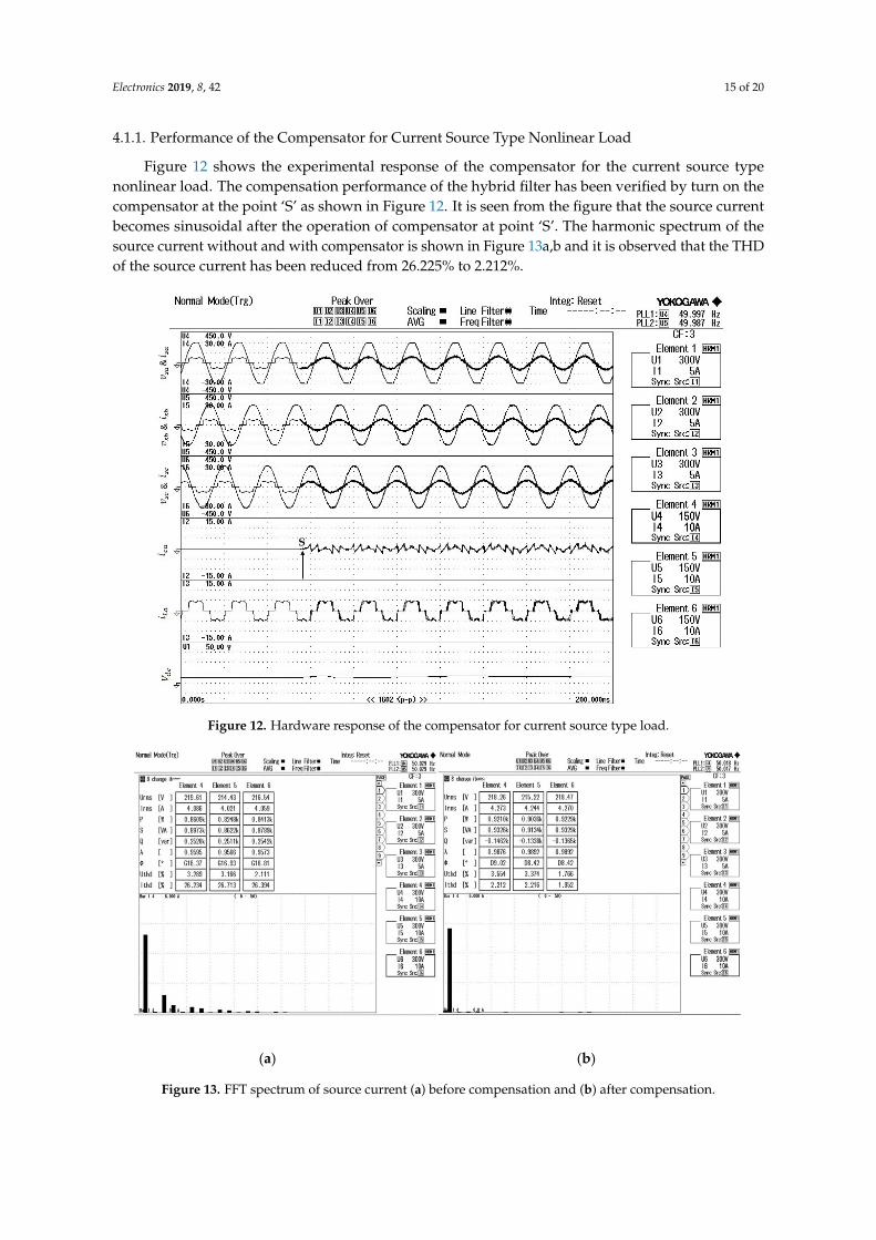
4.1.1. Performance of the Compensator for Current Source Type Nonlinear Load
Figure 12 shows the experimental response of the compensator for the current source type nonlinear load. The compensation performance of the hybrid filter has been verified by turn on the compensator at the point ‘S’ as shown in Figure 12. It is seen from the figure that the source current becomes sinusoidal after the operation of compensator at point ‘S’. The harmonic spectrum of the
Figure 11. Experimental setup.
4.1. Hardware Resultsand Discussion
A series of experiments involving different types of loads and their dynamic variations have beenconducted, and the performance of the compensator has been evaluated. A six-channel YOKOGAWAPower Quality Analyser has been used to capture the signals such as supply voltage, source current,load current, compensator current and DC link voltage. The hardware system parameters are shownin Table 2
Table 2. Experimental circuit parameters.
Active Power Filter Intelligent Power Module (IPM)PEC16DSMO1 with 6 IGBT Switches
IGBT rating 25 A, 1200 VSwitching frequency of APF switches 2 kHz
Current sensors LTS 25-NPVoltage sensors LV 25-PFilter inductors 7 mH and 10 mHFilter capacitors 30 µF and 40 µF
DC link capacitor 6400 µF
Electronics 2019, 8, 42 15 of 20
4.1.1. Performance of the Compensator for Current Source Type Nonlinear Load
Figure 12 shows the experimental response of the compensator for the current source typenonlinear load. The compensation performance of the hybrid filter has been verified by turn on thecompensator at the point ‘S’ as shown in Figure 12. It is seen from the figure that the source currentbecomes sinusoidal after the operation of compensator at point ‘S’. The harmonic spectrum of thesource current without and with compensator is shown in Figure 13a,b and it is observed that the THDof the source current has been reduced from 26.225% to 2.212%.
Electronics 2019, 8, x FOR PEER REVIEW 15 of 20
source current without and with compensator is shown in Figure 13a,b and it is observed that the THD of the source current has been reduced from 26.225% to 2.212%.
Figure 12. Hardware response of the compensator for current source type load.
(a) (b)
Figure 13. FFT spectrum of source current (a) before compensation and (b) after compensation.
4.1.2. Performance of the Compensator for Varying Current Source Type Nonlinear Load
The performance of the hybrid compensator has been verified experimentally by creating a step change in the load current at ‘A’ as shown in Figure 14. It is observed that the source current in all the three phases are sinusoidal and the compensator is able compensate the harmonic distortion even
Figure 12. Hardware response of the compensator for current source type load.
Electronics 2019, 8, x FOR PEER REVIEW 15 of 20
source current without and with compensator is shown in Figure 13a,b and it is observed that the THD of the source current has been reduced from 26.225% to 2.212%.
Figure 12. Hardware response of the compensator for current source type load.
(a) (b)
Figure 13. FFT spectrum of source current (a) before compensation and (b) after compensation.
4.1.2. Performance of the Compensator for Varying Current Source Type Nonlinear Load
The performance of the hybrid compensator has been verified experimentally by creating a step change in the load current at ‘A’ as shown in Figure 14. It is observed that the source current in all the three phases are sinusoidal and the compensator is able compensate the harmonic distortion even
Figure 13. FFT spectrum of source current (a) before compensation and (b) after compensation.
Electronics 2019, 8, 42 16 of 20
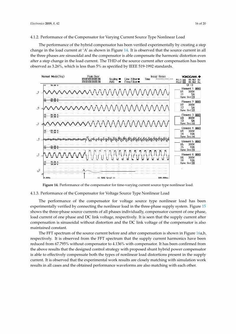
4.1.2. Performance of the Compensator for Varying Current Source Type Nonlinear Load
The performance of the hybrid compensator has been verified experimentally by creating a stepchange in the load current at ‘A’ as shown in Figure 14. It is observed that the source current in allthe three phases are sinusoidal and the compensator is able compensate the harmonic distortion evenafter a step change in the load current. The THD of the source current after compensation has beenobserved as 3.26%, which is less than 5% as specified by IEEE 519-1992 standards.
Electronics 2019, 8, x FOR PEER REVIEW 16 of 20
after a step change in the load current. The THD of the source current after compensation has been observed as 3.26%, which is less than 5% as specified by IEEE 519-1992 standards.
Figure 14. Performance of the compensator for time-varying current source type nonlinear load.
4.1.3. Performance of the Compensator for Voltage Source Type Nonlinear Load
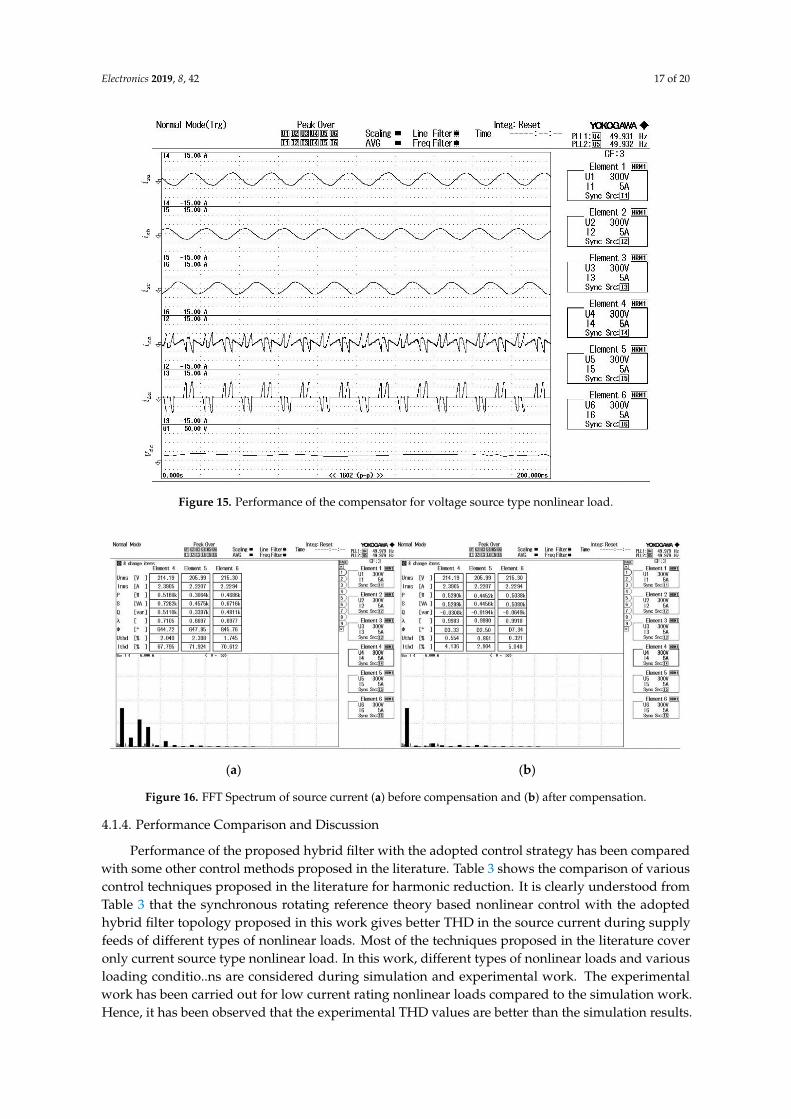
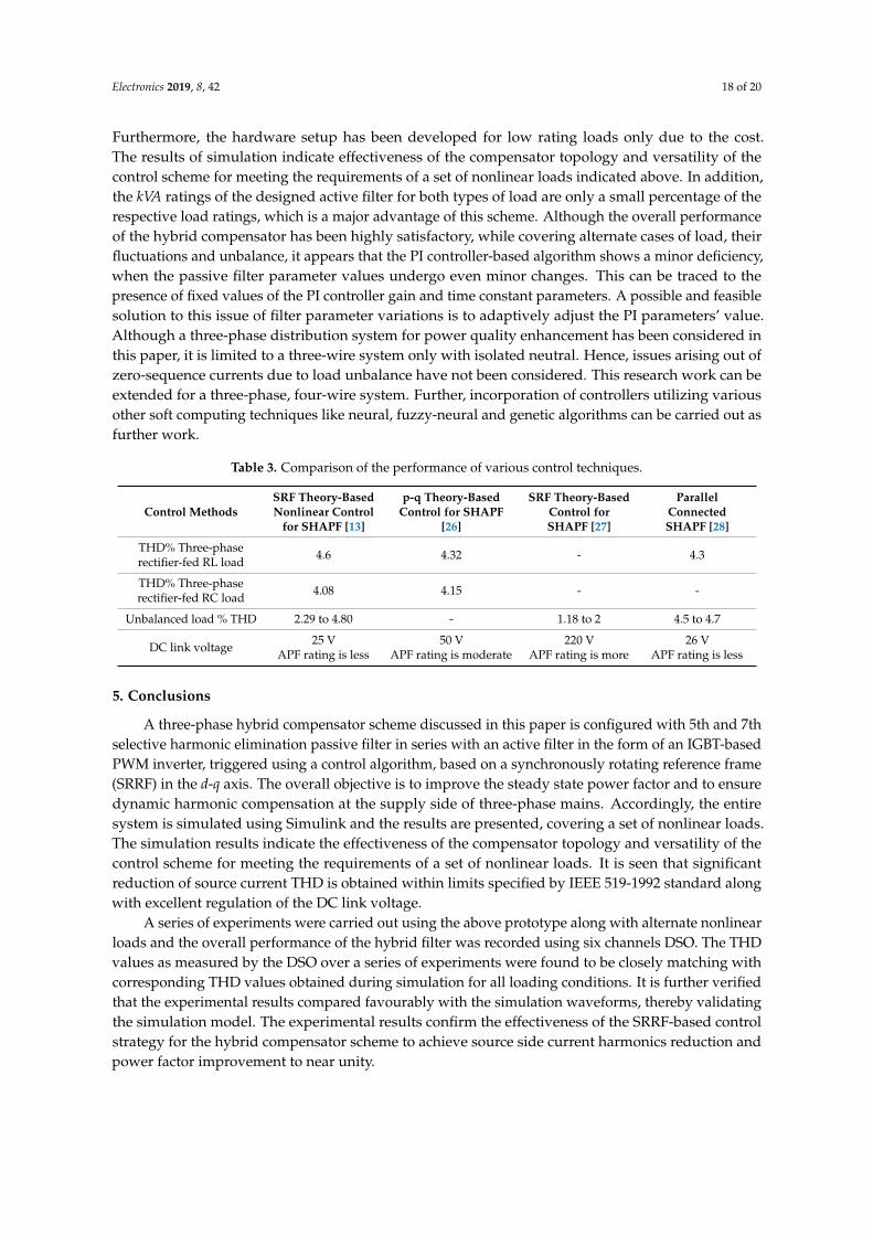
The performance of the compensator for voltage source type nonlinear load has been experimentally verified by connecting the nonlinear load in the three-phase supply system. Figure 15 shows the three-phase source currents of all phases individually, compensator current of one phase, load current of one phase and DC link voltage, respectively. It is seen that the supply current after compensation is sinusoidal without distortion and the DC link voltage of the compensator is also maintained constant.
The FFT spectrum of the source current before and after compensation is shown in Figure 16a,b, respectively. It is observed from the FFT spectrum that the supply current harmonics have been reduced from 67.795% without compensator to 4.136% with compensator. It has been confirmed from the above results that the designed control strategy with proposed shunt hybrid power compensator is able to effectively compensate both the types of nonlinear load distortions present in the supply current. It is observed that the experimental work results are closely matching with simulation work results in all cases and the obtained performance waveforms are also matching with each other.
Figure 14. Performance of the compensator for time-varying current source type nonlinear load.
4.1.3. Performance of the Compensator for Voltage Source Type Nonlinear Load
The performance of the compensator for voltage source type nonlinear load has beenexperimentally verified by connecting the nonlinear load in the three-phase supply system. Figure 15shows the three-phase source currents of all phases individually, compensator current of one phase,load current of one phase and DC link voltage, respectively. It is seen that the supply current aftercompensation is sinusoidal without distortion and the DC link voltage of the compensator is alsomaintained constant.
The FFT spectrum of the source current before and after compensation is shown in Figure 16a,b,respectively. It is observed from the FFT spectrum that the supply current harmonics have beenreduced from 67.795% without compensator to 4.136% with compensator. It has been confirmed fromthe above results that the designed control strategy with proposed shunt hybrid power compensatoris able to effectively compensate both the types of nonlinear load distortions present in the supplycurrent. It is observed that the experimental work results are closely matching with simulation workresults in all cases and the obtained performance waveforms are also matching with each other.
Electronics 2019, 8, 42 17 of 20Electronics 2019, 8, x FOR PEER REVIEW 17 of 20
Figure 15. Performance of the compensator for voltage source type nonlinear load.
(a) (b)
Figure 16. FFT Spectrum of source current (a) before compensation and (b) after compensation.
4.1.4. Performance Comparison and Discussion
Performance of the proposed hybrid filter with the adopted control strategy has been compared with some other control methods proposed in the literature. Table 3 shows the comparison of various control techniques proposed in the literature for harmonic reduction. It is clearly understood from Table 3 that the synchronous rotating reference theory based nonlinear control with the adopted hybrid filter topology proposed in this work gives better THD in the source current during supply feeds of different types of nonlinear loads. Most of the techniques proposed in the literature cover only current source type nonlinear load. In this work, different types of nonlinear loads and various loading conditio..ns are considered during simulation and experimental work. The experimental work has been carried out for low current rating nonlinear loads compared to the simulation work. Hence, it has been observed that the experimental THD values are better than the simulation results. Furthermore, the hardware setup has been developed for low rating loads only due to the cost. The
Figure 15. Performance of the compensator for voltage source type nonlinear load.
Electronics 2019, 8, x FOR PEER REVIEW 17 of 20
Figure 15. Performance of the compensator for voltage source type nonlinear load.
(a) (b)
Figure 16. FFT Spectrum of source current (a) before compensation and (b) after compensation.
4.1.4. Performance Comparison and Discussion
Performance of the proposed hybrid filter with the adopted control strategy has been compared with some other control methods proposed in the literature. Table 3 shows the comparison of various control techniques proposed in the literature for harmonic reduction. It is clearly understood from Table 3 that the synchronous rotating reference theory based nonlinear control with the adopted hybrid filter topology proposed in this work gives better THD in the source current during supply feeds of different types of nonlinear loads. Most of the techniques proposed in the literature cover only current source type nonlinear load. In this work, different types of nonlinear loads and various loading conditio..ns are considered during simulation and experimental work. The experimental work has been carried out for low current rating nonlinear loads compared to the simulation work. Hence, it has been observed that the experimental THD values are better than the simulation results. Furthermore, the hardware setup has been developed for low rating loads only due to the cost. The
Figure 16. FFT Spectrum of source current (a) before compensation and (b) after compensation.
4.1.4. Performance Comparison and Discussion
Performance of the proposed hybrid filter with the adopted control strategy has been comparedwith some other control methods proposed in the literature. Table 3 shows the comparison of variouscontrol techniques proposed in the literature for harmonic reduction. It is clearly understood fromTable 3 that the synchronous rotating reference theory based nonlinear control with the adoptedhybrid filter topology proposed in this work gives better THD in the source current during supplyfeeds of different types of nonlinear loads. Most of the techniques proposed in the literature coveronly current source type nonlinear load. In this work, different types of nonlinear loads and variousloading conditio..ns are considered during simulation and experimental work. The experimentalwork has been carried out for low current rating nonlinear loads compared to the simulation work.Hence, it has been observed that the experimental THD values are better than the simulation results.
Electronics 2019, 8, 42 18 of 20
Furthermore, the hardware setup has been developed for low rating loads only due to the cost.The results of simulation indicate effectiveness of the compensator topology and versatility of thecontrol scheme for meeting the requirements of a set of nonlinear loads indicated above. In addition,the kVA ratings of the designed active filter for both types of load are only a small percentage of therespective load ratings, which is a major advantage of this scheme. Although the overall performanceof the hybrid compensator has been highly satisfactory, while covering alternate cases of load, theirfluctuations and unbalance, it appears that the PI controller-based algorithm shows a minor deficiency,when the passive filter parameter values undergo even minor changes. This can be traced to thepresence of fixed values of the PI controller gain and time constant parameters. A possible and feasiblesolution to this issue of filter parameter variations is to adaptively adjust the PI parameters’ value.Although a three-phase distribution system for power quality enhancement has been considered inthis paper, it is limited to a three-wire system only with isolated neutral. Hence, issues arising out ofzero-sequence currents due to load unbalance have not been considered. This research work can beextended for a three-phase, four-wire system. Further, incorporation of controllers utilizing variousother soft computing techniques like neural, fuzzy-neural and genetic algorithms can be carried out asfurther work.
Table 3. Comparison of the performance of various control techniques.
Unbalanced load % THD 2.29 to 4.80 - 1.18 to 2 4.5 to 4.7
DC link voltage 25 VAPF rating is less
50 VAPF rating is moderate
220 VAPF rating is more
26 VAPF rating is less
5. Conclusions
A three-phase hybrid compensator scheme discussed in this paper is configured with 5th and 7thselective harmonic elimination passive filter in series with an active filter in the form of an IGBT-basedPWM inverter, triggered using a control algorithm, based on a synchronously rotating reference frame(SRRF) in the d-q axis. The overall objective is to improve the steady state power factor and to ensuredynamic harmonic compensation at the supply side of three-phase mains. Accordingly, the entiresystem is simulated using Simulink and the results are presented, covering a set of nonlinear loads.The simulation results indicate the effectiveness of the compensator topology and versatility of thecontrol scheme for meeting the requirements of a set of nonlinear loads. It is seen that significantreduction of source current THD is obtained within limits specified by IEEE 519-1992 standard alongwith excellent regulation of the DC link voltage.
A series of experiments were carried out using the above prototype along with alternate nonlinearloads and the overall performance of the hybrid filter was recorded using six channels DSO. The THDvalues as measured by the DSO over a series of experiments were found to be closely matching withcorresponding THD values obtained during simulation for all loading conditions. It is further verifiedthat the experimental results compared favourably with the simulation waveforms, thereby validatingthe simulation model. The experimental results confirm the effectiveness of the SRRF-based controlstrategy for the hybrid compensator scheme to achieve source side current harmonics reduction andpower factor improvement to near unity.
Electronics 2019, 8, 42 19 of 20
Author Contributions: Conceptualization, R.B. and K.P.; methodology, R.B. and K.P.; software, R.B. and K.P.;validation, R.B., K.P.; and R.S.; formal analysis, R.B.; investigation, R.B. and K.P.; data curation, R.B., andK.P.; writing—original draft preparation, R.B., K.P., R.S. and R.A.; writing—review and editing, R.S. and R.A.;supervision, R.S. and R.A.
Funding: This research received no external funding.
Acknowledgments: Authors wish to express their sincere thanks to acknowledge SASTRA Deemed University,Thanjavur, India 613401 for extending infrastructural support to carry out this work.
Conflicts of Interest: The authors declare no conflict of interest.
Emannuel, A.E.; Horton, W.F.; Reid, W.E.; et al. Effects of harmonics on equipment. IEEE Trans. Power Deliv.1993, 8, 672–680. [CrossRef]
5. Das, J.C. Passive filters-potentialities and limitations. IEEE Trans. Ind. Appl. 2004, 40, 232–241. [CrossRef]6. Singh, B.; Al-Haddad, K.; Chandra, A. A review of active filters for power quality improvement. IEEE Trans.
Ind. Electron. 1999, 46, 960–971. [CrossRef]7. Akagi, H. New trends in active filters for power conditioning. IEEE Trans. Ind. Appl. 1996, 32, 1312–1322.
[CrossRef]8. Lam, C.-S.; Wong, M.-C. Design and Control of Hybrid Active Power Filters; Springer: Berlin, Germany, 2014.9. Singh, B.; Verma, V.; Chandra, A.; Al-Haddad, K. Hybrid filters for power quality improvement.
active techniques. IEEE Trans. Ind. Electron. 2003, 50, 161–170. [CrossRef]11. Samadaei, E.; Lesan, S.; Cherati, S.M. A new schematic for hybrid active power filter controller.
In Proceedings of the 2011 IEEE Applied Power Electronics Colloquium (IAPEC), Johor Bahru, Malaysia,18–19 April 2011; pp. 143–148.
12. Mendalek, N.; Al-Haddad, K.; Fnaiech, F.; Dessaint, L.A. Nonlinear control technique to enhance dynamicperformance of a shunt active power filter. IEE Proc.-Electr. Power Appl. 2003, 150, 373–379. [CrossRef]
13. Rahmani, S.; Hamadi, A.; Mendalek, N.; Al-Haddad, K. A new control technique for three-phase shunthybrid power filter. IEEE Trans. Ind. Electron. 2009, 56, 2904–2915. [CrossRef]
14. Rahmani, S.; Mendalek, N.; Al-Haddad, K. Experimental design of a nonlinear control technique forthree-phase shunt active power filter. IEEE Trans. Ind. Electron. 2010, 57, 3364–3375. [CrossRef]
15. Zouidi, A.; Fnaiech, F.; Al-Haddad, K. Voltage source inverter based three-phase shunt active power filter:Topology, Modeling and control strategies. In Proceedings of the 2006 IEEE International Symposium onIndustrial Electronics, Montreal, QC, Canada, 9–13 July 2006; Volume 2, pp. 785–790.
16. Mendalek, N.; Al-Haddad, K. Modeling and nonlinear control of shunt active power filter in the synchronousreference frame. In Proceedings of the Ninth International Conference on Harmonics and Quality of Power.Proceedings (Cat. No.00EX441), Orlando, FL, USA, 1–4 October 2000; Volume 1, pp. 30–35.
17. Balasubramanian, R.; Sankaran, R.; Palani, S. Simulation and performance evaluation of shunt hybrid powerfilter using fuzzy logic based non-linear control for power quality improvement. Sadhana 2017, 42, 1443–1452.[CrossRef]
18. Palandöken, M.; Aksoy, M.; Tümay, M. Application of fuzzy logic controller to active power filters. Electr. Eng.2004, 86, 191–198. [CrossRef]
19. Dey, P.; Mekhilef, S. Current controllers of active power filter for power quality improvement: A technicalanalysis. Automatika 2015, 56, 42–54. [CrossRef]
20. Unnikrishnan, A.K.; Subhash Joshi, T.G.; Manju, A.S.; Joseph, A. Shunt hybrid active power filter forharmonic mitigation: A practical design approach. Sadhana 2015, 40, 1257–1272.
21. Chauhan, S.K.; Shah, M.C.; Tiwari, R.R.; Tekwani, P.N. Analysis, design and digital implementation of ashunt active power filter with different schemes of reference current generation. IET Power Electron. 2013,7, 627–639. [CrossRef]
22. Cataliotti, A.; Cosentino, V. A Time-domain strategy for the measurement of IEEE standard 1459–2000Power quantities in Non sinusoidal Three–phase and Single–phase systems. IEEE Trans. Power Deliv. 2008,23, 2113–2123. [CrossRef]
23. Cataliotti, A.; Cosentino, V. Disturbing Load Identification in Power Systems: A Single-Point Time–DomainMethod Based on IEEE 1459–2000. IEEE Trans. Instrum. Meas. 2009, 58, 1436–1445. [CrossRef]
25. Golestan, S.; Ge, J.M.; Vasquez, J.; Abusorrah, A.M.; Al-Turki, Y.A. Modeling, Tuning, and PerformanceComparison of Second–Order-Generalized-Integrator–Based FLLs. IEEE Trans. Power Electron. 2018,33, 10229–10239. [CrossRef]
26. Balasubramanian, R.; Palani, S. Simulation and performance evaluation of shunt hybrid power filter forpower quality improvement using PQ theory. Int. J. Electr. Comput. Eng. 2016, 6, 2603–2609. [CrossRef]
27. Dey, P.; Mekhilef, S. Synchronous reference frame based control technique for shunt hybrid active powerfilter under non-ideal voltage. In Proceedings of the 2014 IEEE Innovative Smart Grid Technologies-Asia(ISGT ASIA), Kuala Lumpur, Malaysia, 20–23 May 2014; pp. 481–486.
28. Bhattacharya, A.; Chakraborty, C.; Bhattacharya, S. Parallel-connected shunt hybrid active power filtersoperating at different switching frequencies for improved performance. IEEE Trans. Ind. Electron. 2012,59, 4007–4019. [CrossRef]