Enhanced Optical Dichroism of Graphene Nanoribbons F. Hipolito, 1 A. J. Chaves, 2 R. M. Ribeiro, 2 M. I. Vasilevskiy, 2 Vitor M. Pereira, 1, * and N. M. R. Peres 2, † 1 Graphene Research Centre and Department of Physics, National University of Singapore, 2 Science Drive 3, Singapore 117542 2 Department of Physics and Centre of Physics, University of Minho, Campus of Gualtar, 4710-057, Braga, Portugal (Dated: July 11, 2011) The optical conductivity of graphene nanoribbons is analytical and exactly derived. It is shown that the absence of translational invariance along the transverse direction allows considerable intra- band absorption in a narrow frequency window that varies with the ribbon width, and lies in the THz band for ribbons 10–100 nm wide. In this region the anisotropy in the optical conductivity can be as high as two orders of magnitude, which renders the medium dichroic, and allows near 100% polarizability with just a single layer of graphene. PACS numbers: 81.05.ue,81.05.ue,72.80.Vp,78.67.Wj Introduction Dichroism refers to the ability of some materials to absorb light differently, depending on the polarization state of the incoming wave, and leads to effects such as the rotation of the plane of polarization of light trans- mitted through them [1]. This characteristic is the ba- sis of several elementary optical elements like polarizers, wave retarders, etc., which are essential building blocks in photo-electronics and telecommunications. Dichroism is also widely relevant for substance characterization in fields ranging from spectroscopy, to chemistry, to life sci- ences. A grid of parallelly aligned metallic wires is a well known textbook example of a dichroic system, where unpolarized radiation becomes polarized perpendicularly to the wires, if the wavelength is much larger than the wire separation [2]. This example shows how geometri- cal anisotropy can be engineered to induce dichroism in otherwise isotropic media. Here we unveil the dichroic properties of graphene nanoribbons (GNR), and assess how effective grids of GNRs can be as polarizing elements. The motivation to explore GNRs in this context comes from a conver- gence of several critical properties. First, the optical ab- sorption spectrum of pristine graphene is roughly con- stant over an enormous band of frequencies[3, 4], from the THz to the near UV. This opens the unprecedented prospect of exploring its optical response to develop op- tical elements that can operate predictably and consis- tently in such broad frequency bands. Broadband polar- izers, for example, are a much needed element in photonic circuits for telecommunications, and graphene can play here an important role [5]. Second, the optical absorp- tion of graphene is easily switched on and off by varying the electronic density, which can be easily achieved by electrostatic gating [6]. Third, due to the record breaking * Electronic address: [email protected]† Electronic address: peres@fisica.uminho.pt stiffness of the crystal lattice, one can suspend a graphene sheet and cut a grating of the thinnest nanowires (cur- rently of the order of 10 nm [7]), which opens new av- enues in ultra-narrow gratings, and upon which we base the system depicted in Fig. 1. Fourth, since graphene is metallic and a pure surface, the rich phenomenology associated with surface plasmons/polaritons is certainly unavoidable, further broadening the horizon of possibili- ties for optical applications. Finally, the atomic thickness of graphene results in a transparency of 97.7%. Hence, even if one is able to induce strong absorption along one direction, the overall transmissivity will still be large, which is important to maintain losses under control. Method The natural first step towards such possibilities con- sists in analyzing the intrinsic optical response of GNRs, to which we dedicate the remainder of this paper. We are interested in how the finite transverse dimension af- fects the optical absorption spectrum at low frequen- cies (IR and below), which is rather featureless in bulk graphene[3], but turns out to be richer in nanoribbons. The situation we envisage is depicted in Fig. 1, and con- sists in passing an electromagnetic wave across a grid of GNRs. For definiteness and technical simplicity we restrict our analysis to armchair (AC) nanoribbons, al- though our results do not depend on the specific chiral- ity, as will be clear later. Another important aspect to consider in GNRs has to do with how large edge dis- order is expected to be, and to which extent it might mask the phenomena under discussion. To address this, while at the same time keeping as much analytical con- trol over the results as possible, our calculations involve two steps. First, the frequency-dependent conductivity tensor σ ij (ω) of an AC GNR is derived exactly for free electrons governed by a nearest-neighbor tight-binding Hamiltonian (see below). The only energy scale is the hopping amplitude, t ’ 2.7 eV [8]. We then perform en- semble averages of such σ ij (ω), where the width is the fluctuating parameter, and thus extract the overall re- arXiv:1107.1509v1 [cond-mat.mes-hall] 7 Jul 2011
Transcript
Enhanced Optical Dichroism of Graphene Nanoribbons
F. Hipolito,1 A. J. Chaves,2 R. M. Ribeiro,2 M. I. Vasilevskiy,2 Vitor M. Pereira,1, ∗ and N. M. R. Peres2, †
1Graphene Research Centre and Department of Physics,National University of Singapore, 2 Science Drive 3, Singapore 117542
2Department of Physics and Centre of Physics, University of Minho, Campus of Gualtar, 4710-057, Braga, Portugal(Dated: July 11, 2011)
The optical conductivity of graphene nanoribbons is analytical and exactly derived. It is shownthat the absence of translational invariance along the transverse direction allows considerable intra-band absorption in a narrow frequency window that varies with the ribbon width, and lies in theTHz band for ribbons 10–100 nm wide. In this region the anisotropy in the optical conductivity canbe as high as two orders of magnitude, which renders the medium dichroic, and allows near 100%polarizability with just a single layer of graphene.
PACS numbers: 81.05.ue,81.05.ue,72.80.Vp,78.67.Wj
Introduction
Dichroism refers to the ability of some materials toabsorb light differently, depending on the polarizationstate of the incoming wave, and leads to effects such asthe rotation of the plane of polarization of light trans-mitted through them [1]. This characteristic is the ba-sis of several elementary optical elements like polarizers,wave retarders, etc., which are essential building blocksin photo-electronics and telecommunications. Dichroismis also widely relevant for substance characterization infields ranging from spectroscopy, to chemistry, to life sci-ences.
A grid of parallelly aligned metallic wires is a wellknown textbook example of a dichroic system, whereunpolarized radiation becomes polarized perpendicularlyto the wires, if the wavelength is much larger than thewire separation [2]. This example shows how geometri-cal anisotropy can be engineered to induce dichroism inotherwise isotropic media.
Here we unveil the dichroic properties of graphenenanoribbons (GNR), and assess how effective grids ofGNRs can be as polarizing elements. The motivationto explore GNRs in this context comes from a conver-gence of several critical properties. First, the optical ab-sorption spectrum of pristine graphene is roughly con-stant over an enormous band of frequencies[3, 4], fromthe THz to the near UV. This opens the unprecedentedprospect of exploring its optical response to develop op-tical elements that can operate predictably and consis-tently in such broad frequency bands. Broadband polar-izers, for example, are a much needed element in photoniccircuits for telecommunications, and graphene can playhere an important role [5]. Second, the optical absorp-tion of graphene is easily switched on and off by varyingthe electronic density, which can be easily achieved byelectrostatic gating [6]. Third, due to the record breaking
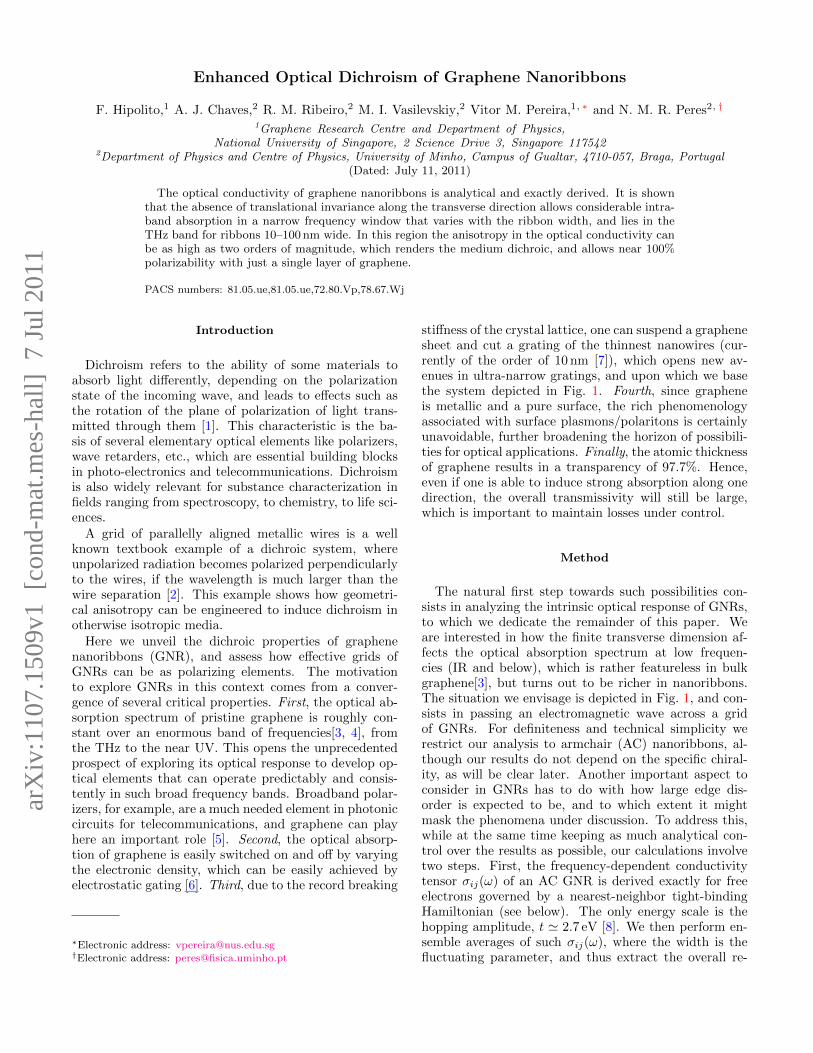
stiffness of the crystal lattice, one can suspend a graphenesheet and cut a grating of the thinnest nanowires (cur-rently of the order of 10 nm [7]), which opens new av-enues in ultra-narrow gratings, and upon which we basethe system depicted in Fig. 1. Fourth, since grapheneis metallic and a pure surface, the rich phenomenologyassociated with surface plasmons/polaritons is certainlyunavoidable, further broadening the horizon of possibili-ties for optical applications. Finally, the atomic thicknessof graphene results in a transparency of 97.7%. Hence,even if one is able to induce strong absorption along onedirection, the overall transmissivity will still be large,which is important to maintain losses under control.
Method
The natural first step towards such possibilities con-sists in analyzing the intrinsic optical response of GNRs,to which we dedicate the remainder of this paper. Weare interested in how the finite transverse dimension af-fects the optical absorption spectrum at low frequen-cies (IR and below), which is rather featureless in bulkgraphene[3], but turns out to be richer in nanoribbons.The situation we envisage is depicted in Fig. 1, and con-sists in passing an electromagnetic wave across a gridof GNRs. For definiteness and technical simplicity werestrict our analysis to armchair (AC) nanoribbons, al-though our results do not depend on the specific chiral-ity, as will be clear later. Another important aspect toconsider in GNRs has to do with how large edge dis-order is expected to be, and to which extent it mightmask the phenomena under discussion. To address this,while at the same time keeping as much analytical con-trol over the results as possible, our calculations involvetwo steps. First, the frequency-dependent conductivitytensor σij(ω) of an AC GNR is derived exactly for freeelectrons governed by a nearest-neighbor tight-bindingHamiltonian (see below). The only energy scale is thehopping amplitude, t ' 2.7 eV [8]. We then perform en-semble averages of such σij(ω), where the width is thefluctuating parameter, and thus extract the overall re-
FIG. 1: Illustration of the device geometry under consideration. consisting of a grid of parallel GNRs perpendicular to theincoming wave. The grid can be in vacuum, at the interface between two different dielectric media, or even inside a metallicwaveguide with sectional area a× b. A plane-polarized incoming wave has its polarization rotated by an angle θ upon crossingthe nanoribbon grating or, alternatively, an unpolarized wave emerges linearly polarized.
sponse of the system accounting for “disorder”. Thisprocedure hinges on the assumption that the leading im-pact of disorder in the optical response is captured bythe broadening of the quasi 1D electronic bands, whichis also achieved with an ensemble average of ribbons withfluctuating width. Moreover, such ensemble averaging isalso close to the experimental situation, insofar as evenstate-of-the-art fabrication cannot control ribbon widthswith atomic precision [9]. Thus, an array of ribbons cutout of a graphene sheet will always display a distributionof widths around a predefined target value 〈W 〉 = W0.Technically, the conductivity of such an array of GNRs isgiven by 〈σij(ω)〉 =
∑W f(W )σWij (ω), where f(W ) is the
normal distribution for the ribbon width W , and σWii (ω)is the conductivity of a single ribbon of width W .
Overall parametrizations are as follows. Ribbons areinterchangeably characterized by their absolute widthW ,or by N , which counts the number of dimer rows alongthe transverse direction, and W =
√3(N − 1)a/2 '
0.12N nm, where a ' 1.42 A represents the C–C dis-tance. For the purposes of ensemble averaging, ribbonwidths are uniformly distributed with a standard devi-ation that we take as constant, 〈N2 − 〈N〉2〉1/2 = 10.All the calculations discussed below have been done atT = 300 K. We use the terms intra- or inter-band in ref-erence to transitions occurring among mini-bands withthe same or opposite sign of energy, respectively. Thehopping amplitude sets the energy scale, and so we putt = 1 throughout. Conductivities are normalized to theuniversal value σ0 = πe2/2h of clean 2D graphene at lowenergies, and the incoming radiation has a wavelengthmuch larger than W .
Anisotropic Optical Absorption
Lateral confinement, reduces the energy spectrum ofGNRs to a set of mini-bands, each reflecting the disper-sion of an effective 1D mode ` (` = 1, 2, . . . , N), propa-gating longitudinally with momentum q: E`,q,λ = λt ε`,q,where λ = ±1, defines the valence and conduction mini-bands,
ε`,q =√
1 + 4 cos k` cos(q/2) + 4 cos2 k`, (1)
and k` = π`/(N+1). Consequently, the density of statesis dominated by Van Hove singularities (VHS) that de-velop at q = 0 in the longitudinal momentum for eachmini-band [10–12]. Such sharp spectral features trans-late in strong optical absorption for ideal GNRs, but arereadily smoothed out by edge or bulk disorder and/ortemperature in real systems. Our ensemble averaginghas the same effect.
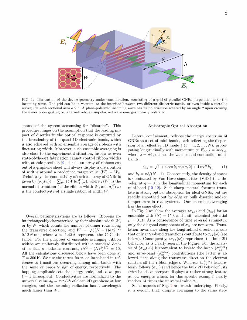
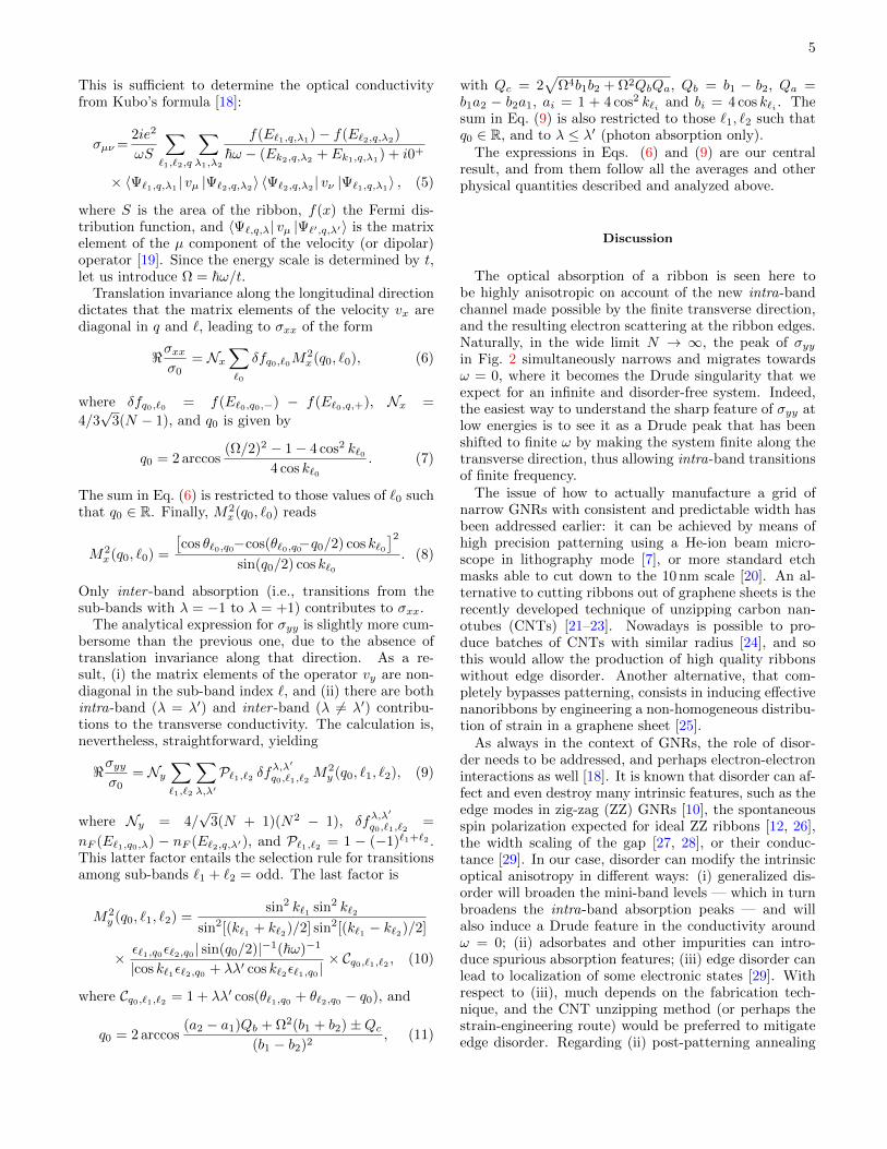
In Fig. 2 we show the averages 〈σxx〉 and 〈σyy〉 for anensemble with 〈N〉 = 150, and finite chemical potentialµ = 0.1t. As a consequence of time reversal symmetry,only the diagonal components of σij are non-zero. Trans-lation invariance along the longitudinal direction meansthat only inter -band transitions contribute to σxx(ω) (seebelow). Consequently, 〈σxx(ω)〉 reproduces the bulk 2Dbehavior, as is clearly seen in the Figure. For the analy-sis of 〈σyy(ω)〉 is convenient to isolate the inter- (σinter
yy )
and intra-band (σintrayy ) contributions (the latter is al-
lowed since along the transverse direction the electronscatters off the ribbon edges). Whereas 〈σinter
yy 〉 feature-lessly follows 〈σxx〉 (and hence the bulk 2D behavior), itsintra-band counterpart displays a rather strong featureat low energies which, for this specific example, nearlyreaches 14 times the universal value σ0.
Some aspects of Fig. 2 are worth underlying. Firstly,it is evident that, despite averaging to the same step-
3
σ ii /
σ0
0
1
2
10
12
14
ℏω/t0 0.1 0.2 0.3 0.4 0.5
σyy (intra)σyy (inter)σxx (inter)
N = 150W ≈ 18 nmμ = 0.1 tT = 300 K
0
1
2
40
50
0 0.1 0.2 0.3 0.4 0.5
FIG. 2: The three non-zero contributions for 〈σii(ω)〉, cal-
culated for 〈N〉 = 150 (' 18.5 nm),⟨N2 − 〈N〉2
⟩1/2= 10,
at T = 300K and µ = 0.1t (' 0.3 eV). The inter -bandcontributions essentially follow the bulk 2D behavior, witha temperature-broadened step onset at ~ω = 2µ. In contrast,the intra-band contribution for the transverse conductivity isstrongly peaked at low energies. The inset shows the samefor a single ribbon of N = 150.
wise ω-dependence, 〈σinteryy (ω)〉 is much smoother than
〈σinterxx (ω)〉, even though the averages are over the same
ensemble. This can be traced to the fact that, for eachindividual ribbon, only N symmetric transitions (−E →+E) contribute to 〈σinter
xx (ω)〉, whereas 〈σinteryy (ω)〉 in-
cludes O(N2) transitions among almost all pairs of mini-bands. Consequently, the latter has many more absorp-tion singularities, but much weaker, by conservation ofspectral weight (this is explicitly shown in the inset ofFig. 2). The averaging is thus more efficient in wash-ing out the structure of VHSs in 〈σinter
yy (ω)〉. Secondly,
the low-energy peak in 〈σintrayy (ω)〉 can be already identi-
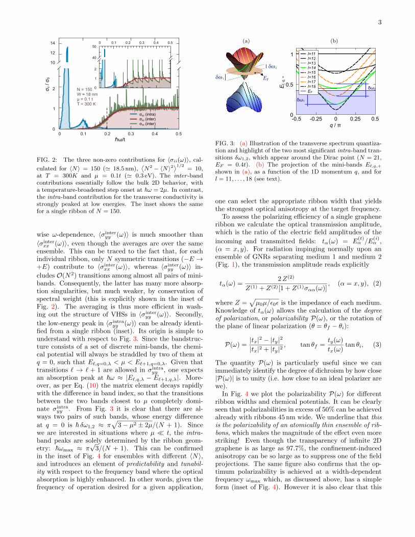
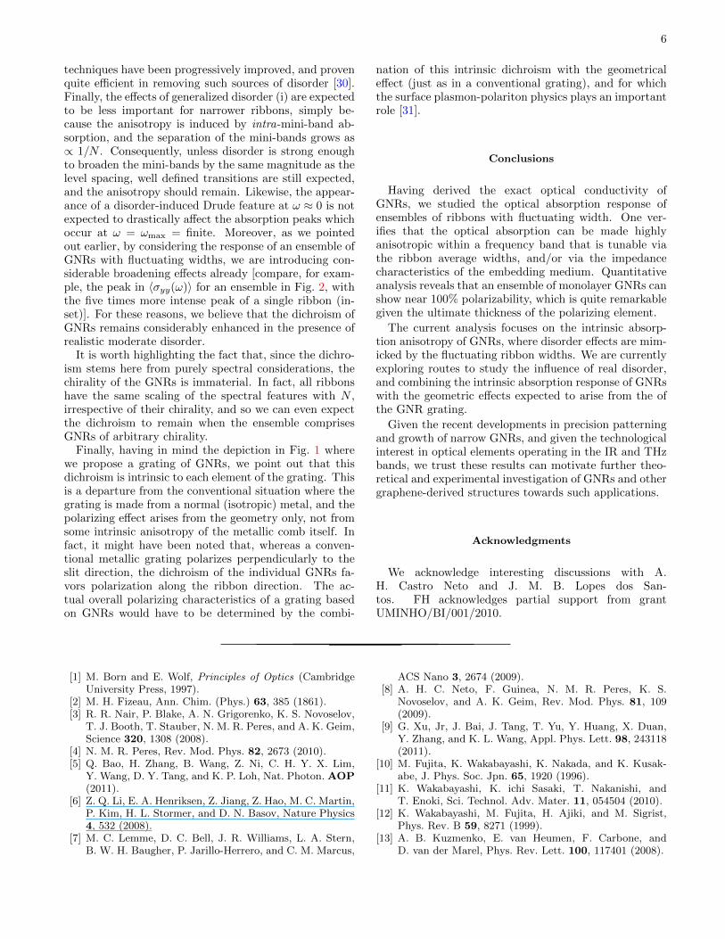
fied from a single ribbon (inset). Its origin is simple tounderstand with respect to Fig. 3. Since the bandstruc-ture consists of a set of discrete mini-bands, the chemi-cal potential will always be straddled by two of them atq = 0, such that E`,q=0,λ < µ < E`+1,q=0,λ. Given thattransitions ` → ` + 1 are allowed in σintra
yy , one expectsan absorption peak at ~ω ≈ |E`,q,λ − E`+1,q,λ|. More-over, as per Eq. (10) the matrix element decays rapidlywith the difference in band index, so that the transitionsbetween the two bands closest to µ completely domi-nate σintra
yy . From Fig. 3 it is clear that there are al-ways two pairs of such bands, whose energy difference
at q = 0 is ~ δω1,2 ≈ π√
3− µ2 ± 2µ/(N + 1). Sincewe are interested in situations where µ t, the intra-band peaks are solely determined by the ribbon geom-etry: ~ωmax ≈ π
√3/(N + 1). This can be confirmed
in the inset of Fig. 4 for ensembles with different 〈N〉,and introduces an element of predictability and tunabil-ity with respect to the frequency band where the opticalabsorption is highly enhanced. In other words, given thefrequency of operation desired for a given application,
(a)
1
2
EF
(b)
E l, q
, +
0
0.5
1
q / π-0.5 -0.25 0 0.25 0.5
δω1
δω 2
l=11l=12l=13l=14l=15l=16l=17l=18EF
δω2
FIG. 3: (a) Illustration of the transverse spectrum quantiza-tion and highlight of the two most significant intra-band tran-sitions δω1,2, which appear around the Dirac point (N = 21,EF = 0.4t). (b) The projection of the mini-bands E`,q,+
shown in (a), as a function of the 1D momentum q, and forl = 11, . . . , 18 (see text).
one can select the appropriate ribbon width that yieldsthe strongest optical anisotropy at the target frequency.
To assess the polarizing efficiency of a single grapheneribbon we calculate the optical transmission amplitude,which is the ratio of the electric field amplitudes of the
incoming and transmitted fields: tα(ω) = E(t)α /E
(i)α ,
(α = x, y). For radiation impinging normally upon anensemble of GNRs separating medium 1 and medium 2(Fig. 1), the transmission amplitude reads explicitly
tα(ω) =2Z(2)
Z(1) + Z(2)[1 + Z(1)σαα(ω)], (α = x, y), (2)
where Z =√µ0µ/ε0ε is the impedance of each medium.
Knowledge of tα(ω) allows the calculation of the degreeof polarization, or polarizability P(ω), or the rotation ofthe plane of linear polarization (θ = θf − θi):
P(ω) =|tx|2 − |ty|2
|tx|2 + |ty|2, tan θf =
ty(ω)
tx(ω)tan θi, (3)
The quantity P(ω) is particularly useful since we canimmediately identify the degree of dichroism by how close|P(ω)| is to unity (i.e. how close to an ideal polarizer arewe).
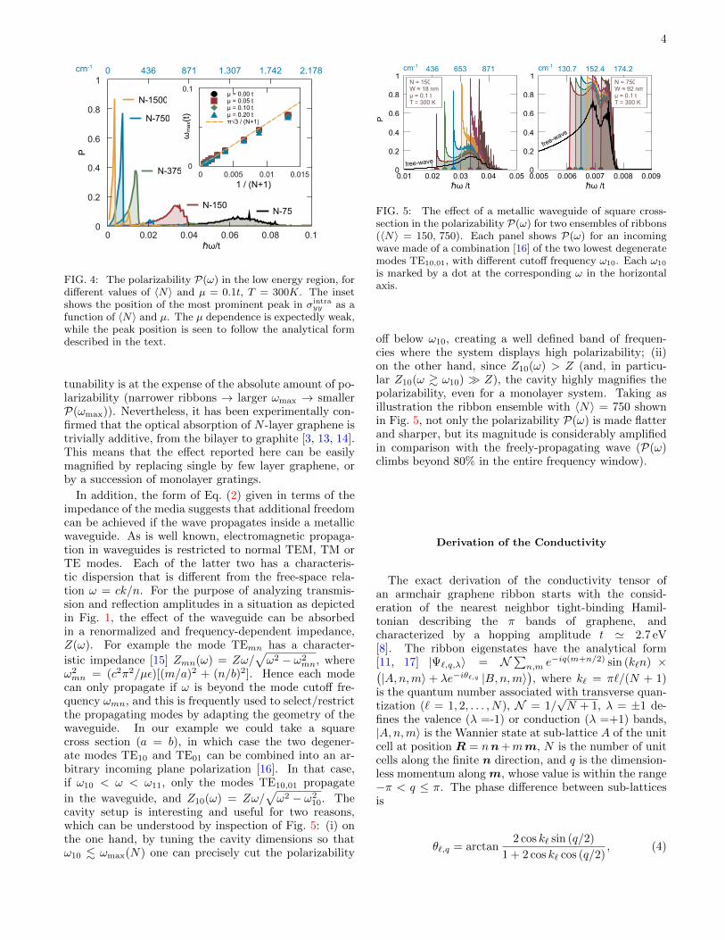
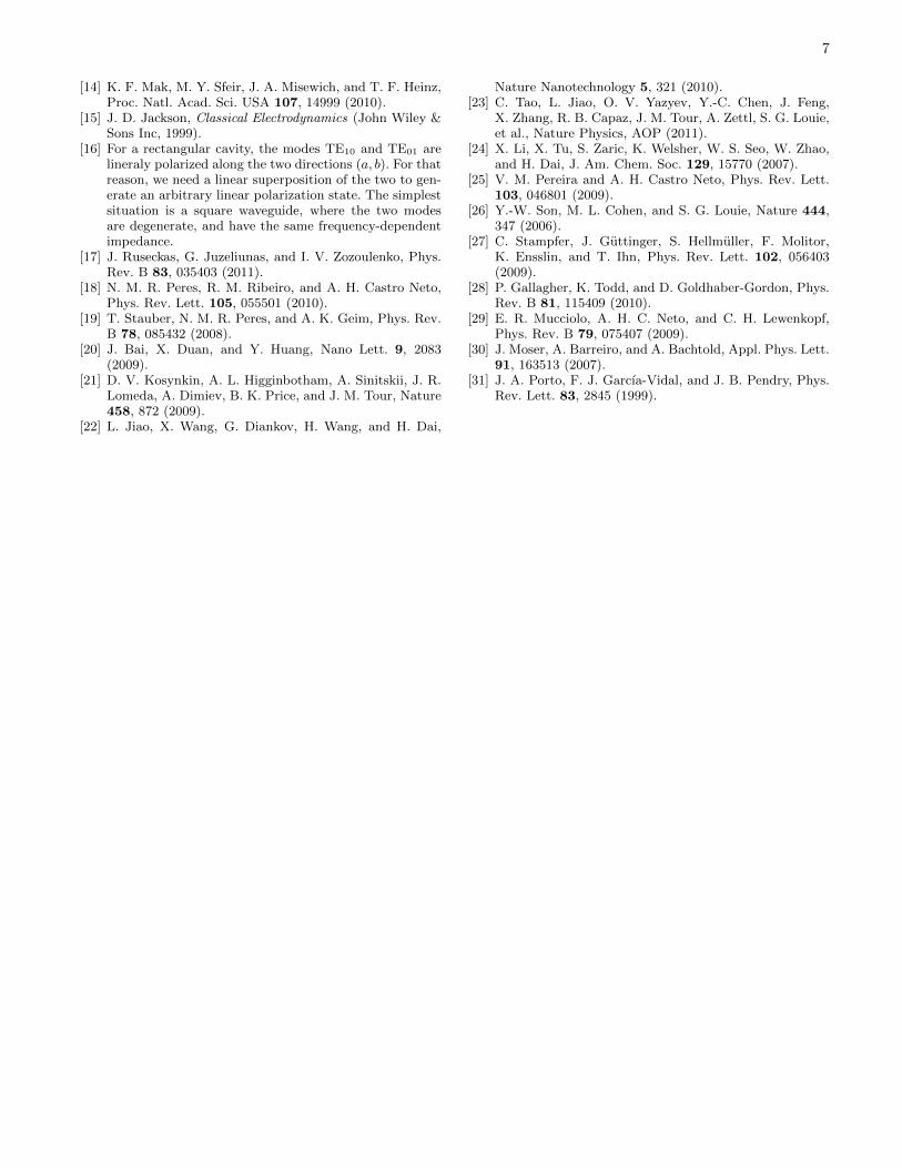
In Fig. 4 we plot the polarizability P(ω) for differentribbon widths and chemical potentials. It can be clearlyseen that polarizabilities in excess of 50% can be achievedalready with ribbons 45 nm wide. We underline that thisis the polarizability of an atomically thin ensemble of rib-bons, which makes the magnitude of the effect even morestriking! Even though the transparency of infinite 2Dgraphene is as large as 97.7%, the confinement-inducedanisotropy can be so large as to suppress one of the fieldprojections. The same figure also confirms that the op-timum polarizability is achieved at a width-dependentfrequency ωmax which, as discussed above, has a simpleform (inset of Fig. 4). However it is also clear that this
FIG. 4: The polarizability P(ω) in the low energy region, fordifferent values of 〈N〉 and µ = 0.1t, T = 300K. The insetshows the position of the most prominent peak in σintra
yy as afunction of 〈N〉 and µ. The µ dependence is expectedly weak,while the peak position is seen to follow the analytical formdescribed in the text.
tunability is at the expense of the absolute amount of po-larizability (narrower ribbons → larger ωmax → smallerP(ωmax)). Nevertheless, it has been experimentally con-firmed that the optical absorption of N -layer graphene istrivially additive, from the bilayer to graphite [3, 13, 14].This means that the effect reported here can be easilymagnified by replacing single by few layer graphene, orby a succession of monolayer gratings.
In addition, the form of Eq. (2) given in terms of theimpedance of the media suggests that additional freedomcan be achieved if the wave propagates inside a metallicwaveguide. As is well known, electromagnetic propaga-tion in waveguides is restricted to normal TEM, TM orTE modes. Each of the latter two has a characteris-tic dispersion that is different from the free-space rela-tion ω = ck/n. For the purpose of analyzing transmis-sion and reflection amplitudes in a situation as depictedin Fig. 1, the effect of the waveguide can be absorbedin a renormalized and frequency-dependent impedance,Z(ω). For example the mode TEmn has a character-
istic impedance [15] Zmn(ω) = Zω/√ω2 − ω2
mn, whereω2mn = (c2π2/µε)[(m/a)2 + (n/b)2]. Hence each mode
can only propagate if ω is beyond the mode cutoff fre-quency ωmn, and this is frequently used to select/restrictthe propagating modes by adapting the geometry of thewaveguide. In our example we could take a squarecross section (a = b), in which case the two degener-ate modes TE10 and TE01 can be combined into an ar-bitrary incoming plane polarization [16]. In that case,if ω10 < ω < ω11, only the modes TE10,01 propagate
in the waveguide, and Z10(ω) = Zω/√ω2 − ω2
10. Thecavity setup is interesting and useful for two reasons,which can be understood by inspection of Fig. 5: (i) onthe one hand, by tuning the cavity dimensions so thatω10 . ωmax(N) one can precisely cut the polarizability
0
0.2
0.4
0.6
0.8
1
ℏω /t0.01 0.02 0.03 0.04 0.05
436 653 871N = 150W ≈ 18 nmμ = 0.1 tT = 300 K
free-wave
cm-1
P
cm-1
0
0.2
0.4
0.6
0.8
1
ℏω /t0.005 0.006 0.007 0.008 0.009
130.7 152.4 174.2
free-wave
N = 750W ≈ 92 nmμ = 0.1 tT = 300 K
FIG. 5: The effect of a metallic waveguide of square cross-section in the polarizability P(ω) for two ensembles of ribbons(〈N〉 = 150, 750). Each panel shows P(ω) for an incomingwave made of a combination [16] of the two lowest degeneratemodes TE10,01, with different cutoff frequency ω10. Each ω10
is marked by a dot at the corresponding ω in the horizontalaxis.
off below ω10, creating a well defined band of frequen-cies where the system displays high polarizability; (ii)on the other hand, since Z10(ω) > Z (and, in particu-lar Z10(ω & ω10) Z), the cavity highly magnifies thepolarizability, even for a monolayer system. Taking asillustration the ribbon ensemble with 〈N〉 = 750 shownin Fig. 5, not only the polarizability P(ω) is made flatterand sharper, but its magnitude is considerably amplifiedin comparison with the freely-propagating wave (P(ω)climbs beyond 80% in the entire frequency window).
Derivation of the Conductivity
The exact derivation of the conductivity tensor ofan armchair graphene ribbon starts with the consid-eration of the nearest neighbor tight-binding Hamil-tonian describing the π bands of graphene, andcharacterized by a hopping amplitude t ' 2.7 eV[8]. The ribbon eigenstates have the analytical form[11, 17] |Ψ`,q,λ〉 = N
∑n,m e
−iq(m+n/2) sin (k`n) ×(|A,n,m〉+ λe−iθ`,q |B,n,m〉
), where k` = π`/(N + 1)
is the quantum number associated with transverse quan-tization (` = 1, 2, . . . , N), N = 1/
√N + 1, λ = ±1 de-
fines the valence (λ =-1) or conduction (λ =+1) bands,|A,n,m〉 is the Wannier state at sub-lattice A of the unitcell at position R = nn+mm, N is the number of unitcells along the finite n direction, and q is the dimension-less momentum along m, whose value is within the range−π < q ≤ π. The phase difference between sub-latticesis
θ`,q = arctan2 cos k` sin (q/2)
1 + 2 cos k` cos (q/2), (4)
5
This is sufficient to determine the optical conductivityfrom Kubo’s formula [18]:
where S is the area of the ribbon, f(x) the Fermi dis-tribution function, and 〈Ψ`,q,λ| vµ |Ψ`′,q,λ′〉 is the matrixelement of the µ component of the velocity (or dipolar)operator [19]. Since the energy scale is determined by t,let us introduce Ω = ~ω/t.
Translation invariance along the longitudinal directiondictates that the matrix elements of the velocity vx arediagonal in q and `, leading to σxx of the form
<σxxσ0
= Nx∑`0
δfq0,`0M2x(q0, `0), (6)
where δfq0,`0 = f(E`0,q0,−) − f(E`0,q,+), Nx =
4/3√
3(N − 1), and q0 is given by
q0 = 2 arccos(Ω/2)2 − 1− 4 cos2 k`0
4 cos k`0. (7)
The sum in Eq. (6) is restricted to those values of `0 suchthat q0 ∈ R. Finally, M2
x(q0, `0) reads
M2x(q0, `0) =
[cos θ`0,q0−cos(θ`0,q0−q0/2) cos k`0
]2sin(q0/2) cos k`0
. (8)
Only inter -band absorption (i.e., transitions from thesub-bands with λ = −1 to λ = +1) contributes to σxx.
The analytical expression for σyy is slightly more cum-bersome than the previous one, due to the absence oftranslation invariance along that direction. As a re-sult, (i) the matrix elements of the operator vy are non-diagonal in the sub-band index `, and (ii) there are bothintra-band (λ = λ′) and inter -band (λ 6= λ′) contribu-tions to the transverse conductivity. The calculation is,nevertheless, straightforward, yielding
<σyyσ0
= Ny∑`1,`2
∑λ,λ′
P`1,`2 δfλ,λ′
q0,`1,`2M2y (q0, `1, `2), (9)
where Ny = 4/√
3(N + 1)(N2 − 1), δfλ,λ′
q0,`1,`2=
nF (E`1,q0,λ) − nF (E`2,q,λ′), and P`1,`2 = 1 − (−1)`1+`2 .This latter factor entails the selection rule for transitionsamong sub-bands `1 + `2 = odd. The last factor is
|cos k`1ε`2,q0 + λλ′ cos k`2ε`1,q0 |× Cq0,`1,`2 , (10)
where Cq0,`1,`2 = 1 + λλ′ cos(θ`1,q0 + θ`2,q0 − q0), and
q0 = 2 arccos(a2 − a1)Qb + Ω2(b1 + b2)±Qc
(b1 − b2)2, (11)
with Qc = 2√
Ω4b1b2 + Ω2QbQa, Qb = b1 − b2, Qa =b1a2 − b2a1, ai = 1 + 4 cos2 k`i and bi = 4 cos k`i . Thesum in Eq. (9) is also restricted to those `1, `2 such thatq0 ∈ R, and to λ ≤ λ′ (photon absorption only).
The expressions in Eqs. (6) and (9) are our centralresult, and from them follow all the averages and otherphysical quantities described and analyzed above.
Discussion
The optical absorption of a ribbon is seen here tobe highly anisotropic on account of the new intra-bandchannel made possible by the finite transverse direction,and the resulting electron scattering at the ribbon edges.Naturally, in the wide limit N → ∞, the peak of σyyin Fig. 2 simultaneously narrows and migrates towardsω = 0, where it becomes the Drude singularity that weexpect for an infinite and disorder-free system. Indeed,the easiest way to understand the sharp feature of σyy atlow energies is to see it as a Drude peak that has beenshifted to finite ω by making the system finite along thetransverse direction, thus allowing intra-band transitionsof finite frequency.
The issue of how to actually manufacture a grid ofnarrow GNRs with consistent and predictable width hasbeen addressed earlier: it can be achieved by means ofhigh precision patterning using a He-ion beam micro-scope in lithography mode [7], or more standard etchmasks able to cut down to the 10 nm scale [20]. An al-ternative to cutting ribbons out of graphene sheets is therecently developed technique of unzipping carbon nan-otubes (CNTs) [21–23]. Nowadays is possible to pro-duce batches of CNTs with similar radius [24], and sothis would allow the production of high quality ribbonswithout edge disorder. Another alternative, that com-pletely bypasses patterning, consists in inducing effectivenanoribbons by engineering a non-homogeneous distribu-tion of strain in a graphene sheet [25].
As always in the context of GNRs, the role of disor-der needs to be addressed, and perhaps electron-electroninteractions as well [18]. It is known that disorder can af-fect and even destroy many intrinsic features, such as theedge modes in zig-zag (ZZ) GNRs [10], the spontaneousspin polarization expected for ideal ZZ ribbons [12, 26],the width scaling of the gap [27, 28], or their conduc-tance [29]. In our case, disorder can modify the intrinsicoptical anisotropy in different ways: (i) generalized dis-order will broaden the mini-band levels — which in turnbroadens the intra-band absorption peaks — and willalso induce a Drude feature in the conductivity aroundω = 0; (ii) adsorbates and other impurities can intro-duce spurious absorption features; (iii) edge disorder canlead to localization of some electronic states [29]. Withrespect to (iii), much depends on the fabrication tech-nique, and the CNT unzipping method (or perhaps thestrain-engineering route) would be preferred to mitigateedge disorder. Regarding (ii) post-patterning annealing
6
techniques have been progressively improved, and provenquite efficient in removing such sources of disorder [30].Finally, the effects of generalized disorder (i) are expectedto be less important for narrower ribbons, simply be-cause the anisotropy is induced by intra-mini-band ab-sorption, and the separation of the mini-bands grows as∝ 1/N . Consequently, unless disorder is strong enoughto broaden the mini-bands by the same magnitude as thelevel spacing, well defined transitions are still expected,and the anisotropy should remain. Likewise, the appear-ance of a disorder-induced Drude feature at ω ≈ 0 is notexpected to drastically affect the absorption peaks whichoccur at ω = ωmax = finite. Moreover, as we pointedout earlier, by considering the response of an ensemble ofGNRs with fluctuating widths, we are introducing con-siderable broadening effects already [compare, for exam-ple, the peak in 〈σyy(ω)〉 for an ensemble in Fig. 2, withthe five times more intense peak of a single ribbon (in-set)]. For these reasons, we believe that the dichroism ofGNRs remains considerably enhanced in the presence ofrealistic moderate disorder.
It is worth highlighting the fact that, since the dichro-ism stems here from purely spectral considerations, thechirality of the GNRs is immaterial. In fact, all ribbonshave the same scaling of the spectral features with N ,irrespective of their chirality, and so we can even expectthe dichroism to remain when the ensemble comprisesGNRs of arbitrary chirality.
Finally, having in mind the depiction in Fig. 1 wherewe propose a grating of GNRs, we point out that thisdichroism is intrinsic to each element of the grating. Thisis a departure from the conventional situation where thegrating is made from a normal (isotropic) metal, and thepolarizing effect arises from the geometry only, not fromsome intrinsic anisotropy of the metallic comb itself. Infact, it might have been noted that, whereas a conven-tional metallic grating polarizes perpendicularly to theslit direction, the dichroism of the individual GNRs fa-vors polarization along the ribbon direction. The ac-tual overall polarizing characteristics of a grating basedon GNRs would have to be determined by the combi-
nation of this intrinsic dichroism with the geometricaleffect (just as in a conventional grating), and for whichthe surface plasmon-polariton physics plays an importantrole [31].
Conclusions
Having derived the exact optical conductivity ofGNRs, we studied the optical absorption response ofensembles of ribbons with fluctuating width. One ver-ifies that the optical absorption can be made highlyanisotropic within a frequency band that is tunable viathe ribbon average widths, and/or via the impedancecharacteristics of the embedding medium. Quantitativeanalysis reveals that an ensemble of monolayer GNRs canshow near 100% polarizability, which is quite remarkablegiven the ultimate thickness of the polarizing element.
The current analysis focuses on the intrinsic absorp-tion anisotropy of GNRs, where disorder effects are mim-icked by the fluctuating ribbon widths. We are currentlyexploring routes to study the influence of real disorder,and combining the intrinsic absorption response of GNRswith the geometric effects expected to arise from the ofthe GNR grating.
Given the recent developments in precision patterningand growth of narrow GNRs, and given the technologicalinterest in optical elements operating in the IR and THzbands, we trust these results can motivate further theo-retical and experimental investigation of GNRs and othergraphene-derived structures towards such applications.
Acknowledgments
We acknowledge interesting discussions with A.H. Castro Neto and J. M. B. Lopes dos San-tos. FH acknowledges partial support from grantUMINHO/BI/001/2010.
[1] M. Born and E. Wolf, Principles of Optics (CambridgeUniversity Press, 1997).
[2] M. H. Fizeau, Ann. Chim. (Phys.) 63, 385 (1861).[3] R. R. Nair, P. Blake, A. N. Grigorenko, K. S. Novoselov,
T. J. Booth, T. Stauber, N. M. R. Peres, and A. K. Geim,Science 320, 1308 (2008).
[4] N. M. R. Peres, Rev. Mod. Phys. 82, 2673 (2010).[5] Q. Bao, H. Zhang, B. Wang, Z. Ni, C. H. Y. X. Lim,
Y. Wang, D. Y. Tang, and K. P. Loh, Nat. Photon. AOP(2011).
[6] Z. Q. Li, E. A. Henriksen, Z. Jiang, Z. Hao, M. C. Martin,P. Kim, H. L. Stormer, and D. N. Basov, Nature Physics4, 532 (2008).
[7] M. C. Lemme, D. C. Bell, J. R. Williams, L. A. Stern,B. W. H. Baugher, P. Jarillo-Herrero, and C. M. Marcus,
ACS Nano 3, 2674 (2009).[8] A. H. C. Neto, F. Guinea, N. M. R. Peres, K. S.
Novoselov, and A. K. Geim, Rev. Mod. Phys. 81, 109(2009).
[9] G. Xu, Jr, J. Bai, J. Tang, T. Yu, Y. Huang, X. Duan,Y. Zhang, and K. L. Wang, Appl. Phys. Lett. 98, 243118(2011).
[10] M. Fujita, K. Wakabayashi, K. Nakada, and K. Kusak-abe, J. Phys. Soc. Jpn. 65, 1920 (1996).
[11] K. Wakabayashi, K. ichi Sasaki, T. Nakanishi, andT. Enoki, Sci. Technol. Adv. Mater. 11, 054504 (2010).
[12] K. Wakabayashi, M. Fujita, H. Ajiki, and M. Sigrist,Phys. Rev. B 59, 8271 (1999).
[13] A. B. Kuzmenko, E. van Heumen, F. Carbone, andD. van der Marel, Phys. Rev. Lett. 100, 117401 (2008).
[14] K. F. Mak, M. Y. Sfeir, J. A. Misewich, and T. F. Heinz,Proc. Natl. Acad. Sci. USA 107, 14999 (2010).
[15] J. D. Jackson, Classical Electrodynamics (John Wiley &Sons Inc, 1999).
[16] For a rectangular cavity, the modes TE10 and TE01 arelineraly polarized along the two directions (a, b). For thatreason, we need a linear superposition of the two to gen-erate an arbitrary linear polarization state. The simplestsituation is a square waveguide, where the two modesare degenerate, and have the same frequency-dependentimpedance.
[17] J. Ruseckas, G. Juzeliunas, and I. V. Zozoulenko, Phys.Rev. B 83, 035403 (2011).
[18] N. M. R. Peres, R. M. Ribeiro, and A. H. Castro Neto,Phys. Rev. Lett. 105, 055501 (2010).
[19] T. Stauber, N. M. R. Peres, and A. K. Geim, Phys. Rev.B 78, 085432 (2008).
[20] J. Bai, X. Duan, and Y. Huang, Nano Lett. 9, 2083(2009).
[21] D. V. Kosynkin, A. L. Higginbotham, A. Sinitskii, J. R.Lomeda, A. Dimiev, B. K. Price, and J. M. Tour, Nature458, 872 (2009).
[22] L. Jiao, X. Wang, G. Diankov, H. Wang, and H. Dai,
Nature Nanotechnology 5, 321 (2010).[23] C. Tao, L. Jiao, O. V. Yazyev, Y.-C. Chen, J. Feng,
X. Zhang, R. B. Capaz, J. M. Tour, A. Zettl, S. G. Louie,et al., Nature Physics, AOP (2011).
[24] X. Li, X. Tu, S. Zaric, K. Welsher, W. S. Seo, W. Zhao,and H. Dai, J. Am. Chem. Soc. 129, 15770 (2007).
[25] V. M. Pereira and A. H. Castro Neto, Phys. Rev. Lett.103, 046801 (2009).
[26] Y.-W. Son, M. L. Cohen, and S. G. Louie, Nature 444,347 (2006).
[27] C. Stampfer, J. Guttinger, S. Hellmuller, F. Molitor,K. Ensslin, and T. Ihn, Phys. Rev. Lett. 102, 056403(2009).
[28] P. Gallagher, K. Todd, and D. Goldhaber-Gordon, Phys.Rev. B 81, 115409 (2010).
[29] E. R. Mucciolo, A. H. C. Neto, and C. H. Lewenkopf,Phys. Rev. B 79, 075407 (2009).
[30] J. Moser, A. Barreiro, and A. Bachtold, Appl. Phys. Lett.91, 163513 (2007).
[31] J. A. Porto, F. J. Garcıa-Vidal, and J. B. Pendry, Phys.Rev. Lett. 83, 2845 (1999).