Date post: | 15-Mar-2023 |
Category: |
Documents |
Upload: | khangminh22 |
View: | 1 times |
Download: | 0 times |
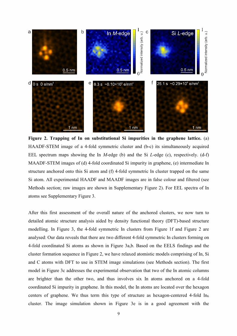
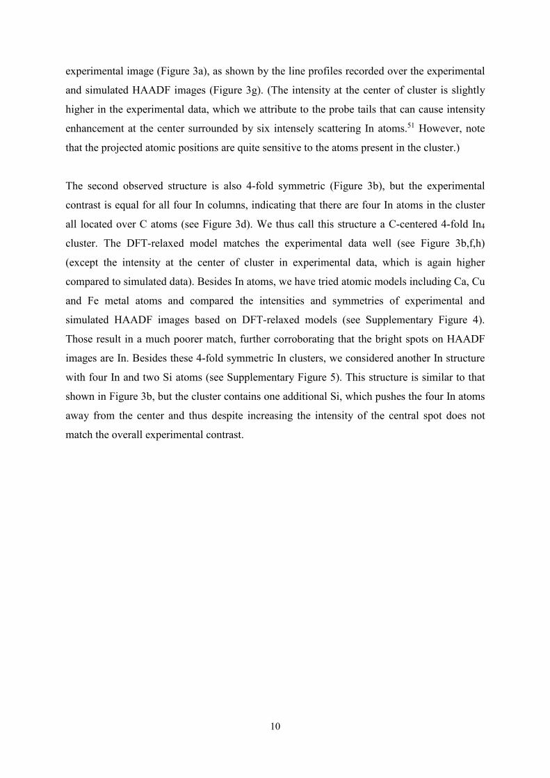
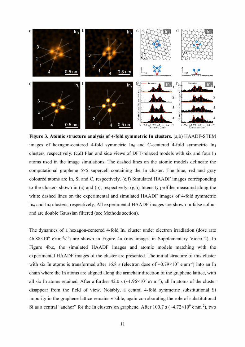
1
Single indium atoms and few-atom indium
clusters anchored onto graphene via silicon
heteroatoms
Kenan Elibol,1,2,3 Clemens Mangler,1 David D. O'Regan,2,4 Kimmo Mustonen,1 Dominik
Eder,5 Jannik C. Meyer,1,6 Jani Kotakoski,1 Richard G. Hobbs,2,3
Toma Susi,1,* Bernhard C. Bayer1,5,*
1Faculty of Physics, University of Vienna, Boltzmanngasse 5, A-1090, Vienna, Austria
2Centre for Research on Adaptive Nanostructures and Nanodevices (CRANN) and the SFI Advanced Materials
and Bio-Engineering Research Centre (AMBER), Dublin 2, Ireland
3School of Chemistry, Trinity College Dublin, The University of Dublin, Dublin 2, Ireland
4School of Physics, Trinity College Dublin, The University of Dublin, Dublin 2, Ireland
5Institute of Materials Chemistry, Vienna University of Technology (TU Wien), Getreidemarkt 9/165, A-1060
Vienna, Austria
6Institute for Applied Physics, University of Tübingen, Auf der Morgenstelle 10, 72076 Tübingen
*Corresponding authors: [email protected], [email protected]
2
Abstract
Single atoms and few-atom nanoclusters are of high interest in catalysis and plasmonics, but
pathways for their fabrication and stable placement remain scarce. We report here the self-
assembly of room-temperature-stable single indium (In) atoms and few-atom In clusters (2-6
atoms) that are anchored to substitutional silicon (Si) impurity atoms in suspended monolayer
graphene membranes. Using atomically resolved scanning transmission electron microscopy
(STEM), we find that the exact atomic arrangements of the In atoms depend strongly on the
original coordination of the Si “anchors” in the graphene lattice: Single In atoms and In
clusters with 3-fold symmetry readily form on 3-fold coordinated Si atoms, whereas 4-fold
symmetric clusters are found attached to 4-fold coordinated Si atoms. All structures are
produced by our fabrication route without the requirement for electron-beam induced
materials modification. In turn, when activated by electron beam irradiation in the STEM, we
observe in situ the formation, restructuring and translation dynamics of the Si-anchored In
structures: Hexagon-centered 4-fold symmetric In clusters can (reversibly) transform into In
chains or In dimers, whereas C-centered 3-fold symmetric In clusters can move along the zig-
zag direction of the graphene lattice due to the migration of Si atoms during electron-beam
irradiation, or transform to Si-anchored single In atoms. Our results provide a novel
framework for the controlled self-assembly and heteroatomic anchoring of single atoms and
few-atom clusters on graphene.
3
Introduction
Supported single atoms and atomic clusters comprised of only few atoms (“nanoclusters”)
have distinct electrical, optical, magnetic and catalytic properties.1–6 These have suggested
single atoms and few-atom clusters to be of high application potential, particularly in
heterogeneous catalysis (“single-atom catalysts” to “few-atom catalysts”)1,2,7–16 as well as in
nanoplasmonics.17,18 For catalysis applications, single atoms and few-atom clusters anchored
to carbon substrates are of particularly high relevance.16,19–24 Shortcomings in fabrication and
synthesis, controlled placement and anchoring, and characterisation in terms of, e.g.,
structure, composition and stability, currently hinder however their further study and use.
An emerging pathway towards both controllable fabrication and concurrent microscopic
imaging of small atomic arrangements is the application of aberration-corrected scanning
transmission electron microscopy (STEM) to atoms that are placed onto or implanted into
suspended two-dimensional (2D) membranes such as graphene.25–29 Controlled placement of
individual impurity atoms within the graphene lattice via the controlled movement of the
STEM electron beam (e-beam) has been demonstrated,30–32 mostly relying on ubiquitous
substitutional Si impurities inherent to chemical vapour deposited (CVD) graphene.33 This
STEM-based manipulation has been expanded towards the study of homoatomic Si clusters in
graphene.34–38 Recently, the merging of such Si clusters with a single Pt atom towards
heteroatomic Pt-Si structures on graphene was also reported.39 A shortcoming of the STEM
manipulation approach is, however, the difficulty in extending it to large scale fabrication. A
materials system that intrinsically and readily allows single-atom and few-atom cluster
formation and anchoring on graphene membranes in a more scalable and self-assembled
fashion has remained elusive to date.
We report here the self-assembly of room-temperature-stable single In atoms (1 atom) and
few-atom In clusters (2-6 atoms) and their concurrent anchoring onto individual substitutional
Si dopant atoms in graphene membranes. We employ atomically resolved and element-
sensitive STEM40 to observe the In-Si structures including probing their structural dynamics
and formation mechanisms in situ via e-beam induced structural rearrangements.41,42 We find
that the original coordination of Si in the graphene lattice is critical for the atomic
arrangement of the In single atoms and clusters. While single In atoms and 3-fold symmetric
4
In clusters form on 3-fold coordinated Si atoms, 4-fold symmetric clusters are found on 4-fold
coordinated Si atoms. Within the 4-fold and 3-fold symmetric clusters, In atoms can be either
located on top of carbon atoms or hexagon centers. Hexagon-centered 4-fold symmetric In6
clusters can dynamically transform into three different structures during e-beam irradiation: a
chain with six In atoms, an In dimer located on a pentagon center, and a dimer located on a
hexagon center. Unlike the 4-fold symmetric clusters which are immobile under electron
irradiation,33 the C-centered 3-fold symmetric In5 clusters can move within the graphene
lattice due to the electron irradiation induced movement of the underlying 3-fold coordinated
Si site. These 3-fold clusters can also transform to anchored single In atoms.
Combined, our observations evidence a large diversity of room-temperature-stable single
atoms and few atom clusters in the In-Si-graphene system and thereby provide a unique
materials system and unprecedented toolbox for the controlled self-assembly and
heteroatomic anchoring of single atoms and few-atom clusters onto graphene.
5
Results The experiments we carried out to deposit indium single atoms and few-atom clusters on
graphene are schematically shown in Figure 1a. A monolayer CVD graphene membrane
suspended over a holey SiN chip is first loaded into the STEM setup (ultra-high vacuum
(UHV) with base pressure ~10-9 mbar) which comprises the microscope and directly coupled
preparation chambers including laser annealing and an in situ evaporation chamber. We note
that CVD graphene intrinsically includes a small number of substitutional Si heteroatoms, as
well-documented in prior literature.33,43,44 The sample is then first irradiated in UHV by 600
mW of laser power at 445 nm wavelength, allowing the removal of adventitious hydrocarbon
adsorbates from the graphene that stem from membrane fabrication and ambient air
exposure.45,46 Subsequently, without vacuum break, In is evaporated onto the graphene
membrane using a custom-built preparation chamber (base pressure ~10-9 mbar).42 After in
situ deposition of In, the sample is transferred into the microscope, without vacuum break,
and once more irradiated in situ by a similar 600 mW laser before STEM imaging. Due to the
low melting point (~160 °C) but low vapor pressure of In,47 the second laser irradiation
critically promotes the diffusion of In atoms over the graphene surface.
During STEM imaging, medium and high angle annular dark field (MAADF and HAADF)
signals are acquired simultaneously. These allow the discrimination of imaged elements based
on signal intensity (our HAADF intensity scales with atomic number as Z~1.6 for isolated
atoms and roughly linear with specimen thickness for a given Z).40 Further elemental
identification is made via simultaneously recorded electron energy loss spectroscopy (EELS)
data. Further experimental details can be found in the Methods section.
Figure 1b-f shows that large atomically clean areas are found on the graphene after In
deposition and the second laser irradiation. The key feature of interest we observe in these
large clean graphene areas are the small bright spots in the MAADF images in Figure 1b-f.
We identify these spots as single In atoms (Figure 1c) and few-atom In clusters formed on the
graphene surface (Figure 1e,f), which are all anchored to the graphene via single
substitutional Si impurity atoms covalently bound within the graphene lattice, as described in
detail below. Notably for the clusters, we consistently observe two different symmetries: 3-
fold and 4-fold. (These symmetries refer to as-observed contrast within the image projection
plane, as typical for (S)TEM measurements. Out-of-plane atom positions in the structures are
6
not readily accessible by STEM, but will be elucidated based on our associated structural
modelling and image simulations).
We stress that the single In atoms and In clusters are already present before extended STEM
imaging, i.e. they are generally not produced by the electron irradiation, but have self-
assembled during In evaporation and the second laser anneal prior to imaging. In the fields of
view in Figure 1b,d (with electron irradiation dose rates of 0.73×10⁶ e-nm-2s-1 (b), 0.18×10⁶ e-
nm-2s-1 (d)), the In structures appear to be unperturbed by STEM imaging. We verify the
structure of these In clusters on graphene at higher magnification in the next sections.
Imaging at higher magnifications is associated with higher electron dose rates, however,
which drives structural modifications of the In structures by energy transfer from the scanning
e-beam,41,42 but at the same time also allows us to in situ probe their structural dynamics.
To verify the chemical nature of the structures, an EEL spectrum image is acquired on a
typical cluster shown in the HAADF image of Figure 2a. EELS accumulated with an energy
range focused on the In M- and Si L-edges show that the cluster consists of In and Si atoms
(Figure 2b,c). The EELS data indicates 4-fold symmetry for the positions of In around a
rather central Si signal. This is a first hint to the Si-anchoring of the In atoms on the graphene
lattice. From the EELS map, however, it remains unclear if the Si signal is from one or
several central Si atoms.
Towards addressing this question, the HAADF image sequence in Figure 2d-f (see also
Supplementary Video 1) reveals the self-assembly process of the Si-In structures (here
emulated by the energy input from the e-beam). This sequence has been acquired at a higher
magnification (and thus higher electron dose rate of 20.83×10⁶ e-nm-2s-1) than Figure 1b,d and
thereby enables observation of e-beam induced structural dynamics.41,42 In particular, Figure
2d shows initially a bare 4-fold coordinated Si atom in the graphene lattice. After 8.3 s
(electron dose 0.1×10⁹ e-nm-2), In atoms have become trapped at this Si atom to form an
intermediate Si-anchored In structure (Figure 2e, further details on this intermediate possible
dimer structure are discussed below in Figure 4). After 25.1 s (Figure 2f, electron dose
0.29×10⁹ e/nm2), additional In atoms have become trapped to eventually form a 4-fold
symmetric In cluster anchored to the 4-fold Si atom in the graphene lattice (further details on
the structure below).
7
This observation of In cluster formation suggests that a single central Si atom is present in the
observed In cluster structures. Notably, no In reservoir is present within the field of view
around the Si atom during cluster formation in Figure 2d-f. This excludes a direct role of the
electron beam in moving the In atoms from an reservoir towards the Si during STEM
scanning.48 Instead, Figure 2d-f suggests a self-assembly formation mechanism for the In
clusters in which In atoms or moieties constantly diffuse across the graphene membrane (with
much higher diffusion speed than resolvable by STEM41,49), and become trapped during
encounters with the substitutional Si, thereby self-assembling into the observed Si-anchored
In clusters on the graphene. We suggest that this facile self-assembly relies on the significant
mobility50 of In atoms on the graphene membrane at room temperature (resulting from In’s
low melting point (~160 °C) and low vapor pressure over a wide temperature range47) and the
higher reactivity of the Si site compared to the relatively inert graphene lattice.
8
Figure 1. Overview of In single atom and cluster anchoring on graphene. (a) Schematic
illustration of the experiment involving laser irradiation, in situ In deposition, and imaging by
STEM. The blue, red and grey coloured atoms are In, Si and C, respectively. (b,d) Large-area
MAADF-STEM images of a clean monolayer graphene surface after in situ deposition,
showing single In atom (b) and few-atom In clusters (d). (c,e,f) Close-up MAADF-STEM
images of a single In atom and 3-fold and 4-fold symmetric In clusters indicated by white
dashed frames in (b,d). All images display false colour and images in (c,e,f) are double
Gaussian filtered after Wiener filtering to reduce noise and enhance contrast (see Methods
section; raw images are shown in Supplementary Figure 1). Note that the contrast of the
underlying graphene lattice is low compared to the clusters, making it difficult to display both
clearly in some of our figures.
9
Figure 2. Trapping of In on substitutional Si impurities in the graphene lattice. (a)
HAADF-STEM image of a 4-fold symmetric cluster and (b-c) its simultaneously acquired
EEL spectrum maps showing the In M-edge (b) and the Si L-edge (c), respectively. (d-f)
MAADF-STEM images of (d) 4-fold coordinated Si impurity in graphene, (e) intermediate In
structure anchored onto this Si atom and (f) 4-fold symmetric In cluster trapped on the same
Si atom. All experimental HAADF and MAADF images are in false colour and filtered (see
Methods section; raw images are shown in Supplementary Figure 2). For EEL spectra of In
atoms see Supplementary Figure 3.
After this first assessment of the overall nature of the anchored clusters, we now turn to
detailed atomic structure analysis aided by density functional theory (DFT)-based structure
modelling. In Figure 3, the 4-fold symmetric In clusters from Figure 1f and Figure 2 are
analysed: Our data reveals that there are two different 4-fold symmetric In clusters forming on
4-fold coordinated Si atoms as shown in Figure 3a,b. Based on the EELS findings and the
cluster formation sequence in Figure 2, we have relaxed atomistic models comprising of In, Si
and C atoms with DFT to use in STEM image simulations (see Methods section). The first
model in Figure 3c addresses the experimental observation that two of the In atomic columns
are brighter than the other two, and thus involves six In atoms anchored on a 4-fold
coordinated Si impurity in graphene. In this model, the In atoms are located over the hexagon
centers of graphene. We thus term this type of structure as hexagon-centered 4-fold In6
cluster. The image simulation shown in Figure 3e is in a good agreement with the
10
experimental image (Figure 3a), as shown by the line profiles recorded over the experimental
and simulated HAADF images (Figure 3g). (The intensity at the center of cluster is slightly
higher in the experimental data, which we attribute to the probe tails that can cause intensity
enhancement at the center surrounded by six intensely scattering In atoms.51 However, note
that the projected atomic positions are quite sensitive to the atoms present in the cluster.)
The second observed structure is also 4-fold symmetric (Figure 3b), but the experimental
contrast is equal for all four In columns, indicating that there are four In atoms in the cluster
all located over C atoms (see Figure 3d). We thus call this structure a C-centered 4-fold In4
cluster. The DFT-relaxed model matches the experimental data well (see Figure 3b,f,h)
(except the intensity at the center of cluster in experimental data, which is again higher
compared to simulated data). Besides In atoms, we have tried atomic models including Ca, Cu
and Fe metal atoms and compared the intensities and symmetries of experimental and
simulated HAADF images based on DFT-relaxed models (see Supplementary Figure 4).
Those result in a much poorer match, further corroborating that the bright spots on HAADF
images are In. Besides these 4-fold symmetric In clusters, we considered another In structure
with four In and two Si atoms (see Supplementary Figure 5). This structure is similar to that
shown in Figure 3b, but the cluster contains one additional Si, which pushes the four In atoms
away from the center and thus despite increasing the intensity of the central spot does not
match the overall experimental contrast.
11
Figure 3. Atomic structure analysis of 4-fold symmetric In clusters. (a,b) HAADF-STEM
images of hexagon-centered 4-fold symmetric In6 and C-centered 4-fold symmetric In4
clusters, respectively. (c,d) Plan and side views of DFT-relaxed models with six and four In
atoms used in the image simulations. The dashed lines on the atomic models delineate the
computational graphene 5×5 supercell containing the In cluster. The blue, red and gray
coloured atoms are In, Si and C, respectively. (e,f) Simulated HAADF images corresponding
to the clusters shown in (a) and (b), respectively. (g,h) Intensity profiles measured along the
white dashed lines on the experimental and simulated HAADF images of 4-fold symmetric
In6 and In4 clusters, respectively. All experimental HAADF images are shown in false colour
and are double Gaussian filtered (see Methods section).
The dynamics of a hexagon-centered 4-fold In6 cluster under electron irradiation (dose rate
46.88×10⁶ e-nm-2s-1) are shown in Figure 4a (raw images in Supplementary Video 2). In
Figure 4b,c, the simulated HAADF images and atomic models matching with the
experimental HAADF images of the cluster are presented. The initial structure of this cluster
with six In atoms is transformed after 16.8 s (electron dose of ~0.79×10⁹ e-nm-2) into an In
chain where the In atoms are aligned along the armchair direction of the graphene lattice, with
all six In atoms retained. After a further 42.0 s (~1.96×10⁹ e-nm-2), all In atoms of the cluster
disappear from the field of view. Notably, a central 4-fold symmetric substitutional Si
impurity in the graphene lattice remains visible, again corroborating the role of substitutional
Si as a central “anchor” for the In clusters on graphene. After 100.7 s (~4.72×10⁹ e-nm-2), two
12
In atoms are again captured by the Si atom (similar as in the cluster formation sequence in
Figure 2d-f) and located over the pentagon centers of the 4-fold Si impurity site. After 117.4 s
(~5.50×10⁹ e-nm-2), these two In atoms rotate by 90° to overlay the graphene hexagon centers.
However, they return back to their initial position by again rotating 90° after 125.8 s
(~5.90×10⁹ e-nm-2). This structure finally attracts four additional In atoms after 167.8 s
(~7.86×10⁹ e-nm-2) to form the hexagon-centered 4-fold In6 cluster, identical to that observed
in the first frame of the sequence.
Figure 4. Dynamics of hexagon-centered 4-fold symmetric In6 cluster under e-beam
exposure. (a) HAADF-STEM images acquired at successive times, corresponding to
increasing irradiation doses (indicated over the panels). (b) HAADF image simulations
corresponding to the experimental images in (a). (c) Plan and side views of DFT-relaxed
models with In clusters anchored on the 4-fold coordinated Si impurity in graphene. All
experimental HAADF images are in false colour and double Gaussian filtered (see Methods
section). The scale bars are 0.3 nm.
In addition to indium clusters formed on 4-fold coordinated Si impurities, we observe 3-fold
symmetric In clusters as well as single In atoms anchored on 3-fold coordinated Si impurities,
as shown in detail in Figure 5. Similar to the 4-fold symmetric cases, In atoms in 3-fold
symmetric clusters may be located over the graphene C atoms or hexagon centers, and there
are two distinct variants, here differing by the intensity of the central atomic column. We term
these the C-centered 3-fold In5 cluster (see Figure 5a,b) and the hexagon-centered 3-fold In3
13
cluster (see Figure 5g,h). Notably the hexagon-centered 3-fold In3 structure includes two Si
atoms, one of which is substitutional in the graphene lattice and one which is part of the In
cluster. As shown in Figure 5a-c and g-i, the DFT-relaxed models and experimental data are
in a good agreement.
Under e-beam exposure at higher magnifications, the In atoms in these 3-fold clusters can be
readily ejected by the focused electron beam (see Figure 5a,d, and g,j, also Supplementary
Videos 3, 4, 5 and 6). HAADF-STEM images in Figure 5d show a single In atom anchored on
the 3-fold coordinated Si impurity after the other In atoms are removed from the 3-fold In5
cluster. Notably, although four In atoms are removed, the remaining single In atom keeps its
position on the Si atom under electron irradiation (see Supplementary Videos 4, 5 and 6). In
addition to the model shown in Figure 5b, we have created two different models with four and
five In atoms and compared them with the experimental data (see Supplementary Figure 6).
As shown in Supplementary Figure 6d, the atomic structure shown in Figure 5b is in a better
agreement with the experimental image intensity.
Unlike C-centered 3-fold In5, in the hexagon-centered 3-fold In3 cluster only the anchoring Si
impurity remains in the graphene lattice after removal of three In atoms (see also EEL spectra
in Supplementary Figure 7). (We attempted to relax a C-centered 3-fold symmetric In3
cluster, i.e. without an In or Si atom directly on top of the Si impurity, see Supplementary
Figure 8, but the spacing of the cluster and the intensity of the center column do not match the
experimental data.)
We note that, intermittently, also short-term capturing of single In atoms by 4-fold Si
impurities is observed (Supplementary Figure 9), albeit these arrangements are never as stable
as in the case of 3-fold Si anchoring. We also note that when the coordination of the Si atom
in the graphene lattice is changed due to e-beam exposure, trapping of different structures on
the same Si atom is observed. For instance, in Supplementary Figure 10 a 3-fold symmetric In
cluster is first trapped by a 3-fold coordinated Si atom, then again removed, after which the Si
atom switches into 4-fold coordination, which eventually enables the trapping of an In2 dimer.
After having identified the various observed structures of the In-Si-graphene system, we can
semi-quantitatively elucidate their relative formation probabilities by measuring their areal
observation densities when imaged at wide fields of view (i.e. without inducing structural
14
dynamics with a higher e-beam dose rate; the total number of observations was 43). Note that
observed areal densities of bare 4-fold coordinated Si (0.82/1000 nm-2) and bare 3-fold
coordinated Si (0.89/1000 nm-2) anchoring heteroatoms in the graphene lattice are roughly
similar for our samples. In descending order we find the most often observed (thus most
readily formed and, arguably, most stable) Si-anchored In structures to be as follows:
hexagon-centered 4-fold symmetric In6 clusters (0.37/1000 nm-2), single In atom anchored on
Si (0.32/1000 nm-2), hexagon-centered In3 3-fold symmetric clusters (0.22/1000 nm-2), C-
centered 3-fold symmetric In5 clusters (0.15/1000 nm-2), In2 dimers (0.12/1000 nm-2), and In6
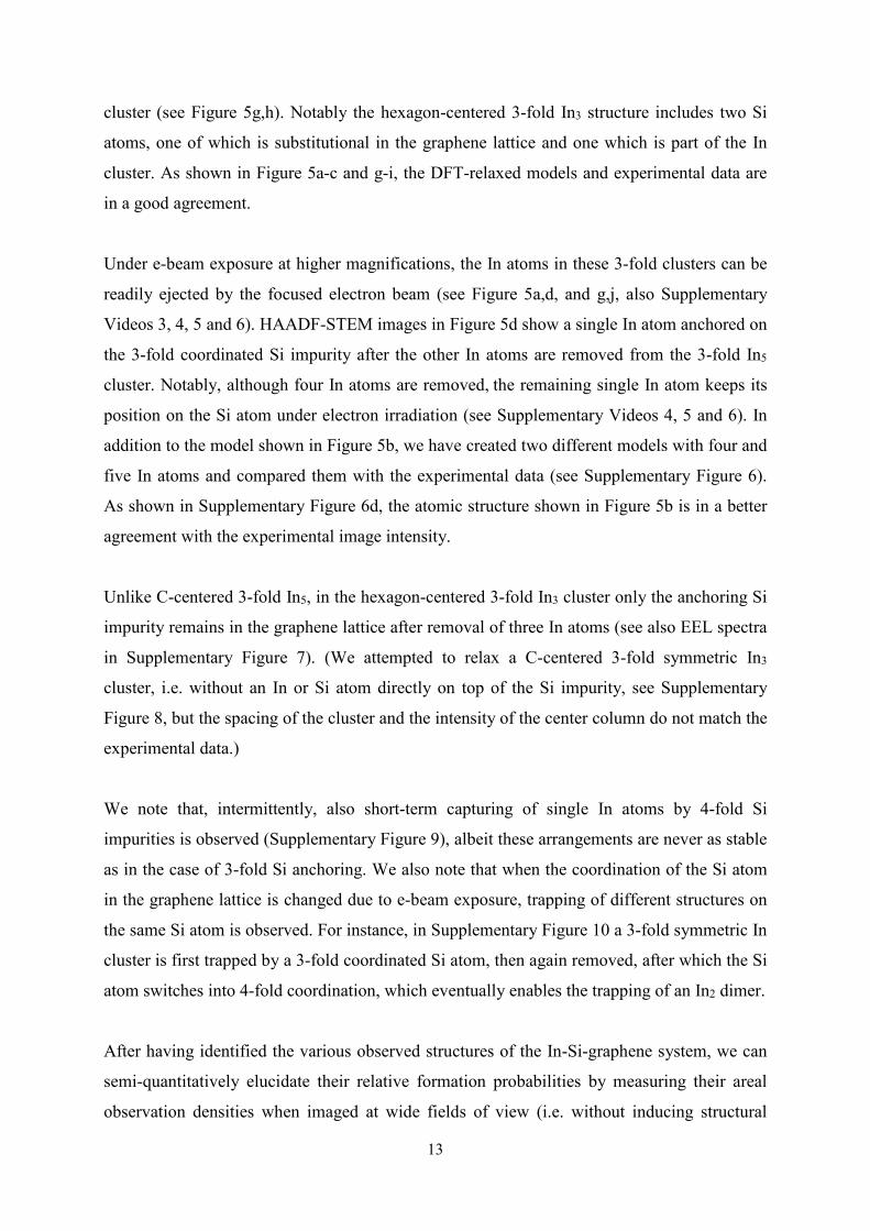
chains (0.07/1000 nm-2). These statistics underline that both In single atoms and few-atom
clusters are well stabilized by the Si-graphene system.
Figure 5. Atomic structure analysis of 3-fold symmetric In clusters. (a,d,g,j) HAADF-
STEM images of (a) a C-centered 3-fold symmetric In5 cluster and (d) In1 single atom (the
same area as in (a) after four In atoms are removed during electron irradiation at a dose of
~0.29×10⁹ e-nm-2) as well as (g) hexagon-centered 3-fold symmetric In3 cluster and (j) Si1 in
graphene lattice (the same area as in (g) after three In atoms surrounding the central Si atom
are removed during electron irradiation at a dose of ~0.39×10⁹ e-nm-2), respectively. Semi-
transparent simulated HAADF images corresponding the structures shown in panels b, e, h
15
and k are shown on the right side of line profiles in white dashed frames on panels a, d, g and
j (left side of line profiles display raw image). The experimental images are in false colour
and Wiener filtered (raw images are shown in Supplementary Figure 11). (b,e,h,k) Plan and
side views of the DFT-relaxed models used for the image simulations shown in panels a, d, g
and j, respectively. The blue, red and grey coloured atoms shown in the atomic models are In,
Si and C, respectively. (c,f,i,l) Intensity profiles recorded along the semi-transparent white
lines overlaid on the experimental and simulated HAADF images in (a,d,g,j). The identity of
the Si site was verified by EELS (Supplementary Figure 7).
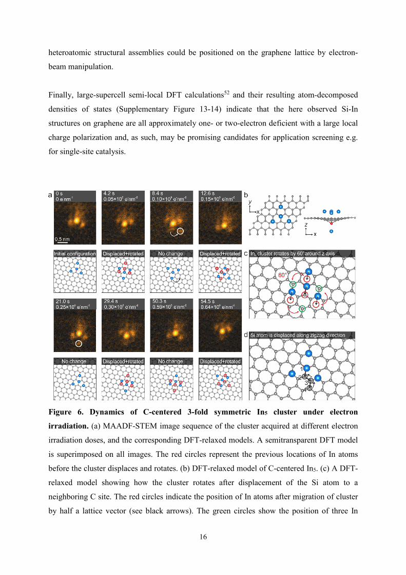
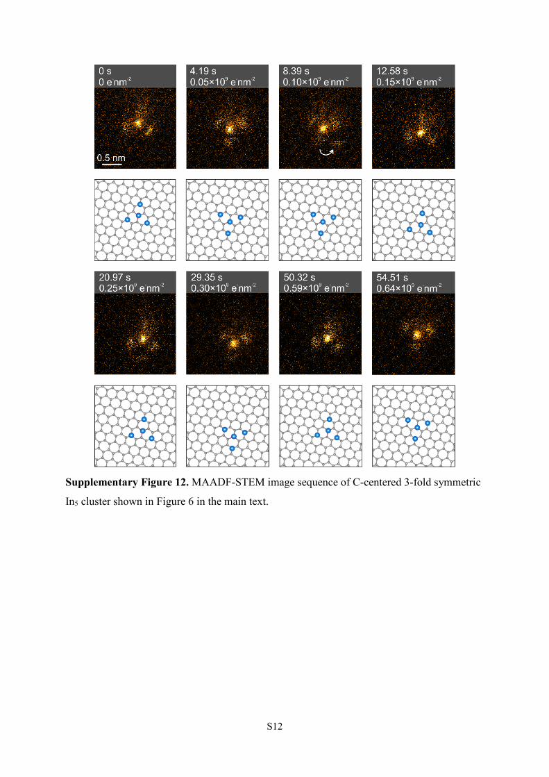
When irradiated by the e-beam at higher dose rates (smaller fields of view), we not only
observe cluster formation and structural dynamics within the In clusters (Figures 2, 4, 5) but
for some also translation/migration in their entirety along the graphene lattice: While the
hexagon-centered In3 clusters are not observed to change their position during e-beam
irradiation (see Supplementary Video 3), we show in Figure 6a the dynamics of a C-centered
In5 3-fold symmetric In cluster during irradiation (see also Supplementary Video 7). From its
initial position, the cluster moves after 4.2 s (~0.05×10⁹ e-nm-2) with respect to the graphene
lattice. The movement of the cluster is due to the migration of the Si impurity to a
neighboring C site along the zig-zag direction of graphene, presumably via the same bond
inversion mechanism as Si impurity manipulation.33 The initial positions of the In atoms are
marked by red circles in the DFT-relaxed model corresponding to the structure acquired at 4.2
s (~0.05×10⁹ e-nm-2). (Note that the Si atom is not visible in the model due to the In atom
located on top of it.) The change in the location of the Si changes the alignment of the In
atoms with respect to the graphene lattice, and thus the entire cluster migrates to preserve its
bonding. The movement of the cluster continues after 8.4 s (~0.10×10⁹ e-nm-2). In the
HAADF image, an additional In contrast appears below the cluster (same effect is visible in
the frame at 21.0 s at a dose of ~0.25×10⁹ e-nm-2). We believe this is because the cluster
rotated before the scan was finished, which suggested acquiring STEM images at a higher
scan speed. Although we were not able to resolve the rotation direction of the cluster,
additional In contrast does appear on the HAADF image at 8.4 s (~0.10×10⁹ e-nm-2)
suggesting that the cluster rotates 60° anticlockwise around the center (see also
Supplementary Figure 12). Until the last image frame acquired after 54.5 s (~0.64×10⁹ e-nm-
2), the Si atom and the cluster has jumped five times along the zig-zag direction of the
graphene lattice (see path in Figure 6d). Although beyond the scope of this work, this
observation sequence suggests that not only single atoms,31 but also more complex
16
heteroatomic structural assemblies could be positioned on the graphene lattice by electron-
beam manipulation.
Finally, large-supercell semi-local DFT calculations52 and their resulting atom-decomposed
densities of states (Supplementary Figure 13-14) indicate that the here observed Si-In
structures on graphene are all approximately one- or two-electron deficient with a large local
charge polarization and, as such, may be promising candidates for application screening e.g.
for single-site catalysis.
Figure 6. Dynamics of C-centered 3-fold symmetric In5 cluster under electron
irradiation. (a) MAADF-STEM image sequence of the cluster acquired at different electron
irradiation doses, and the corresponding DFT-relaxed models. A semitransparent DFT model
is superimposed on all images. The red circles represent the previous locations of In atoms
before the cluster displaces and rotates. (b) DFT-relaxed model of C-centered In5. (c) A DFT-
relaxed model showing how the cluster rotates after displacement of the Si atom to a
neighboring C site. The red circles indicate the position of In atoms after migration of cluster
by half a lattice vector (see black arrows). The green circles show the position of three In
17
atoms surrounding the center after the rotation of the cluster by 60°. (d) The same model as in
(c), showing the initial configuration of the In5 cluster and the sites that the cluster occupies
under electron irradiation. Firstly, the center of the cluster moves step by step from position 1
to 4 (see black circles), and then it migrates back from position 4 to 2. The black arrows show
the direction of movement. The experimental images are in false colour and Wiener filtered
(raw images are shown in Supplementary Figure 12).
Conclusion
We report the self-assembly and anchoring of single In atoms and few-atom In clusters onto
substitutional Si impurity atoms in suspended monolayer graphene membranes. A variety of
structure types that are stable at room temperature are found from our facile fabrication route
without the requirement for e-beam induced materials modification. Most frequently observed
structures are hexagon-centered 4-fold symmetric In6 clusters, single In atoms anchored on Si,
and hexagon-centered 3-fold symmetric In3 clusters. Notably, the original coordination of the
Si determines the atomic arrangements of the In structures: While single In atoms and 3-fold
symmetric In clusters form on 3-fold coordinated Si impurities, 4-fold symmetric clusters are
found on 4-fold coordinated Si impurities. Due to energy transfer from the scanning e-beam,
in higher dose rate close-up imaging we observe in situ the formation, structural changes and
translation dynamics of the Si-anchored In structures on graphene: The hexagon-centered In6
4-fold symmetric clusters transform into three different structures during e-beam irradiation,
including In chains and dimers. Unlike the 4-fold symmetric clusters, the C-centered In5 3-
fold symmetric clusters can move under e-beam irradiation along the zigzag direction of
graphene lattice, and also transform to single In atoms anchored on the Si. The observed Si-
anchored In structures on graphene are promising for future application screening in, e.g.,
catalysis. Combined, our results provide a first materials system and framework towards the
controlled self-assembly and heteroatomic anchoring of single metal atoms and few-atom
clusters on graphene.
18
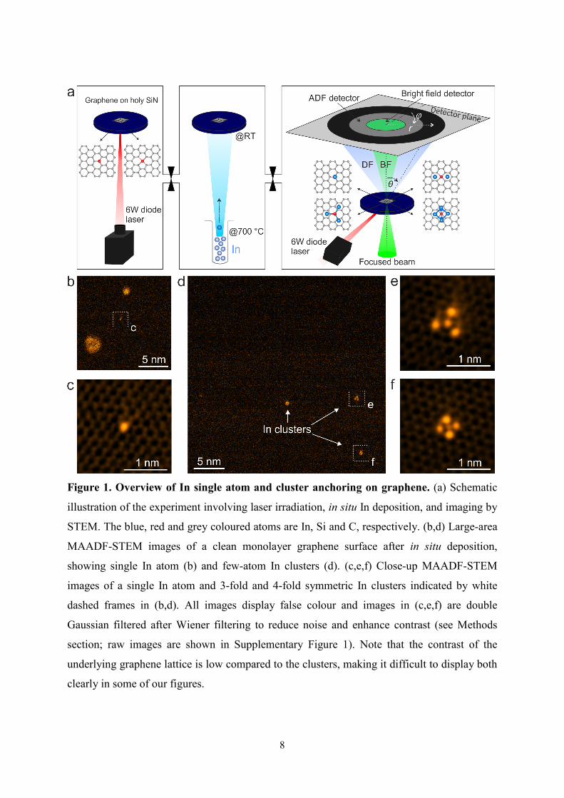
Methods STEM and EELS measurements. STEM images were acquired with a Nion UltraSTEM100 operated at a 60 kV accelerating voltage in UHV (~10-9 mbar) using concurrent high angle annular dark field (HAADF) and medium angle annular dark field (MAADF) detectors with collection angles of 80–300 mrad and 60–80 mrad, respectively. The EELS experiments were carried out by a Gatan PEELS 666 spectrometer retrofitted with an Andor iXon 897 electron-multiplying charge-coupled device camera. The energy dispersion, the beam current and the EELS collection semi-angle were 0.5-1 eV per channel, 30 pA and 35 mrad, respectively.53 The STEM is equipped with a custom-made sample loading and transfer system to enable direct transfer of samples from various preparation chambers into the STEM without exposure to ambient.54,55 In situ laser cleaning. A tunable 6 W diode laser (445 nm, Lasertack GmbH) was used to clean the graphene surfaces. Laser irradiation of the sample held in a transfer arm was performed through a viewport in both STEM and UHV sample preparation chambers. In the experiments, the laser was operated at 10% duty cycle reducing the laser power to 600 mW, which does not induce structural damage in graphene but is sufficient for cleaning.45,46 In situ In deposition. The in situ evaporation of In was achieved using a custom-built preparation chamber (base pressure ~10-9 mbar) coupled to the STEM. The evaporation source was a Knudsen cell with In pellets (99.99% purity, Kurt J. Lesker), which were heated to 700 °C. The resulting In flux was then directed at the graphene sample, which was not intentionally heated. Nominally deposited In thickness was monitored using a quartz micro balance and kept to ~10 nm. Substrates used for In deposition were commercial CVD graphene (Graphenea Inc.) suspended on perforated silicon nitride grids (Ted Pella Inc.). Subsequent to in situ In evaporation, a second in situ laser cleaning step was applied to the sample. STEM image simulations. HAADF and MAADF image simulations were carried out using the QSTEM software with parameters corresponding to the experiments:56 chromatic aberration coefficient of 1 mm, a spherical aberration coefficient of 1 μm, energy spread of 0.48 eV. HAADF and MAADF detector angle ranges are set to the experimental range of 80–300 mrad and 60–80 mrad, respectively. Image processing. ADF images were processed to reduce noise and increase contrast via double Gaussian filtering40, in some cases after applying Wiener filtering. The parameters used for double Gaussian filtering are σ1 = 0.25, σ2 = 0.20, weight = 0.3 (for Figure 1c,e,f), σ1 = 0.25, σ2 = 0.22, weight = 0.25 (for Figure 2a), σ1 = 0.25, σ2 = 0.22, weight = 0.25 (for Figure 2e-g), σ1 = 0.36, σ2 = 0.26, weight = 0.20 (for Figure 3a), σ1 = 0.32, σ2 = 0.25, weight = 0.15 (for Figure 3b) and σ1 = 0.35, σ2 = 0.26, weight = 0.30 (for Figure 4).For the images in
19
Figure 1, Figure 5 and Figure 6, the low-pass Wiener filter57 was applied. In addition, we used false coloring with the ImageJ lookup table ”Orange Hot”. DFT simulations. Density functional theory (DFT) simulations were carried out using the grid-based projector-augmented wave (GPAW) software package58 to study the properties of the supercells of monolayer graphene with Si impurities and adsorbed In clusters. The atomic structures were relaxed with the PBE functional and periodic boundary conditions (with >10 Å of vacuum in the perpendicular direction between the images) in the LCAO mode58 with the grid spacing of 0.2 Å and a 5 × 5 × 1 k-point mesh so that maximum forces were <0.02 eV Å-
1.59 For details of large-supercell density of states calculations52, see Supplementary Figures 13-14.
Acknowledgements K.E., C.M. and B.C.B. acknowledge support from the Austrian Research Promotion Agency (FFG) under project 860382-VISION. T.S. acknowledges funding by the European Research Council (ERC) under the European Union’s Horizon 2020 research and innovation programme (grant agreement no. 756277-ATMEN). D.D.OR. acknowledges the support of Science Foundation Ireland (SFI) through The Advanced Materials and Bioengineering Research Centre (AMBER, grant 12/RC/2278 P2), and of the European Regional Development Fund (ERDF), and further acknowledges Trinity Centre for High Performance Computing and Science Foundation Ireland, for the maintenance and funding, respectively, of the Boyle (Cuimhne upgrade) cluster on which DFT calculations were performed. R.G.H acknowledges the support of Science Foundation Ireland (SFI) through The Advanced Materials and Bioengineering Research Centre (AMBER, grant 12/RC/2278_2) and the Royal Society-Science Foundation Ireland University Research Fellowship (15/RS-URF/3306).
Author contributions K.E. and B.C.B conceived the idea. K.E. performed the experiments and analysed the data. C.M., J.K. and J.C.M. built the setup to carry out the experiments. K.M. helped in sample preparation. D.D.OR. performed large-scale DFT simulations. D.E. and R.H. provided input to data interpretation. J.K. provided input to and T.S. led the DFT-based structure analysis. B.C.B. supervised the project. K.E., T.S. and B.C.B. drafted the manuscript with input from all authors.
20
References
1. Liu, L. & Corma, A. Metal catalysts for heterogeneous catalysis: from single atoms to
nanoclusters and nanoparticles. Chemical reviews 118, 4981–5079 (2018).
2. Tyo, E. C. & Vajda, S. Catalysis by clusters with precise numbers of atoms. Nature
Nanotechnology 10, 577–588 (2015).
3. Grandjean, D. et al. Origin of the bright photoluminescence of few-atom silver clusters confined
in LTA zeolites. Science 361, 686–690 (2018).
4. Sattler, K., Mühlbach, J. & Recknagel, E. Generation of Metal Clusters Containing from 2 to 500
Atoms. Phys. Rev. Lett. 45, 821–824 (1980).
5. Röthlisberger, U., Andreoni, W. & Parrinello, M. Structure of nanoscale silicon clusters. Phys.
Rev. Lett. 72, 665–668 (1994).
6. Scheerder, J. E. et al. Decorating graphene with size-selected few-atom clusters: a novel approach
to investigate graphene–adparticle interactions. Nanoscale 9, 10494–10501 (2017).
7. Yang, X.-F. et al. Single-atom catalysts: a new frontier in heterogeneous catalysis. Accounts of
chemical research 46, 1740–1748 (2013).
8. Liu, J. Catalysis by supported single metal atoms. Acs Catalysis 7, 34–59 (2017).
9. Zhang, W. & Zheng, W. Single atom excels as the smallest functional material. Advanced
Functional Materials 26, 2988–2993 (2016).
10. Chen, Y., Huang, Z., Ma, Z., Chen, J. & Tang, X. Fabrication, characterization, and stability of
supported single-atom catalysts. Catalysis Science & Technology 7, 4250–4258 (2017).
11. Zhang, H., Liu, G., Shi, L. & Ye, J. Single‐atom catalysts: emerging multifunctional materials in
heterogeneous catalysis. Advanced Energy Materials 8, 1701343 (2018).
12. Jakub, Z. et al. Local Structure and Coordination Define Adsorption in a Model Ir1/Fe3O4 Single‐
Atom Catalyst. Angewandte Chemie 131, 14099–14106 (2019).
13. Vats, N. et al. Substrate-Selective Morphology of Cesium Iodide Clusters on Graphene. ACS
Nano 14, 4626–4635 (2020).
14. Hamilton, J. F. & Baetzold, R. C. Catalysis by Small Metal Clusters. Science 205, 1213–1220
(1979).
15. Judai, K., Abbet, S., Wörz, A. S., Heiz, U. & Henry, C. R. Low-Temperature Cluster Catalysis. J.
Am. Chem. Soc. 126, 2732–2737 (2004).
16. Sun, S. et al. Single-atom catalysis using Pt/graphene achieved through atomic layer deposition.
Scientific reports 3, 1–9 (2013).
17. Morton, S. M., Silverstein, D. W. & Jensen, L. Theoretical studies of plasmonics using electronic
structure methods. Chemical reviews 111, 3962–3994 (2011).
21
18. Zhou, W. et al. Atomically localized plasmon enhancement in monolayer graphene. Nature
nanotechnology 7, 161–165 (2012).
19. Rivera‐Cárcamo, C. & Serp, P. Single atom catalysts on carbon‐based materials. ChemCatChem
10, 5058–5091 (2018).
20. Zhang, X. et al. Catalytically active single-atom niobium in graphitic layers. Nature
communications 4, 1–7 (2013).
21. Cheng, N. et al. Platinum single-atom and cluster catalysis of the hydrogen evolution reaction.
Nature communications 7, 1–9 (2016).
22. Chen, Z. et al. Stabilization of single metal atoms on graphitic carbon nitride. Advanced
Functional Materials 27, 1605785 (2017).
23. Li, H., Zhang, H., Yan, X., Xu, B. & Guo, J. Carbon-supported metal single atom catalysts. New
Carbon Materials 33, 1–11 (2018).
24. Zhang, L. et al. Atomic layer deposited Pt-Ru dual-metal dimers and identifying their active sites
for hydrogen evolution reaction. Nature communications 10, 1–11 (2019).
25. Kalinin, S. V. & Pennycook, S. J. Single-atom fabrication with electron and ion beams: From
surfaces and two-dimensional materials toward three-dimensional atom-by-atom assembly. MRS
Bulletin 42, 637–643 (2017).
26. Susi, T., Meyer, J. C. & Kotakoski, J. Manipulating low-dimensional materials down to the level
of single atoms with electron irradiation. Ultramicroscopy 180, 163–172 (2017).
27. Susi, T. et al. Towards atomically precise manipulation of 2D nanostructures in the electron
microscope. 2D Materials 4, 042004 (2017).
28. Dyck, O. et al. Atom-by-atom fabrication with electron beams. Nature Reviews Materials 4, 497–
507 (2019).
29. Xu, T., Shen, Y., Yin, K. & Sun, L. Precisely monitoring and tailoring 2D nanostructures at the
atomic scale. APL Materials 7, 050901 (2019).
30. Dyck, O., Kim, S., Kalinin, S. V. & Jesse, S. Placing single atoms in graphene with a scanning
transmission electron microscope. Applied Physics Letters 111, 113104 (2017).
31. Tripathi, M. et al. Electron-beam manipulation of silicon dopants in graphene. Nano letters 18,
5319–5323 (2018).
32. Su, C. et al. Engineering single-atom dynamics with electron irradiation. Science advances 5,
eaav2252 (2019).
33. Susi, T. et al. Silicon–carbon bond inversions driven by 60-keV electrons in graphene. Physical
Review Letters 113, 115501 (2014).
34. Lee, J., Zhou, W., Pennycook, S. J., Idrobo, J.-C. & Pantelides, S. T. Direct visualization of
reversible dynamics in a Si 6 cluster embedded in a graphene pore. Nature communications 4, 1–7
(2013).
22
35. Yang, Z. et al. Direct observation of atomic dynamics and silicon doping at a topological defect in
graphene. Angewandte Chemie International Edition 53, 8908–8912 (2014).
36. Chen, Q. et al. Rotating anisotropic crystalline silicon nanoclusters in graphene. ACS nano 9,
9497–9506 (2015).
37. Dyck, O. et al. Building structures atom by atom via electron beam manipulation. Small 14,
1801771 (2018).
38. Hofer, C. et al. Direct visualization of the 3D structure of silicon impurities in graphene. Applied
Physics Letters 114, 053102 (2019).
39. Dyck, O. et al. Electron-beam introduction of heteroatomic Pt–Si structures in graphene. Carbon
161, 750–757 (2020).
40. Krivanek, O. L. et al. Atom-by-atom structural and chemical analysis by annular dark-field
electron microscopy. Nature 464, 571–574 (2010).
41. Bayer, B. C. et al. Atomic-Scale in Situ Observations of Crystallization and Restructuring
Processes in Two-Dimensional MoS2 Films. ACS Nano 12, 8758–8769 (2018).
42. Elibol, K. et al. Process Pathway Controlled Evolution of Phase and Van‐der‐Waals Epitaxy in
In/In2O3 on Graphene Heterostructures. Advanced Functional Materials 30, 2003300 (2020).
43. Ramasse, Q. M. et al. Probing the Bonding and Electronic Structure of Single Atom Dopants in
Graphene with Electron Energy Loss Spectroscopy. Nano Lett. 13, 4989–4995 (2013).
44. Zhou, W. et al. Direct Determination of the Chemical Bonding of Individual Impurities in
Graphene. Phys. Rev. Lett. 109, 206803 (2012).
45. Tripathi, M. et al. Cleaning graphene: Comparing heat treatments in air and in vacuum. physica
status solidi (RRL)–Rapid Research Letters 11, 1700124 (2017).
46. Niggas, A. et al. The role of contaminations in ion beam spectroscopy with freestanding 2D
materials: A study on thermal treatment. J. Chem. Phys. 153, 014702 (2020).
47. Zayed, M., Hegazy, M. & Elsayed-Ali, H. Melting and solidification of indium nanocrystals on
(002) graphite. Thin Solid Films 449, 254–263 (2004).
48. Dyck, O. et al. Electron-beam introduction of heteroatomic Pt–Si structures in graphene. Carbon
(2020).
49. Hansen, L. P., Johnson, E., Brorson, M. & Helveg, S. Growth mechanism for single-and multi-
layer MoS2 nanocrystals. The Journal of Physical Chemistry C 118, 22768–22773 (2014).
50. Orudzhov, A. K. Diffusion of indium atoms into iridium through an intermediate graphite
monolayer. Phys. Metals Metallogr. 113, 771–773 (2012).
51. Cui, K. et al. Aberration-corrected STEM and EELS of semiconducting nanostructures. J. Phys.:
Conf. Ser. 326, 012007 (2011).
52. Prentice, J. C. A. et al. The ONETEP linear-scaling density functional theory program. J. Chem.
Phys. 152, 174111 (2020).
23
53. Susi, T. et al. Single-atom spectroscopy of phosphorus dopants implanted into graphene. 2D
Materials 4, 021013 (2017).
54. Mittelberger, A., Kramberger, C. & Meyer, J. C. Insights into radiation damage from atomic
resolution scanning transmission electron microscopy imaging of mono-layer CuPcCl16 films on
graphene. Scientific Reports 8, 4813 (2018).
55. Leuthner, G. T. et al. Scanning transmission electron microscopy under controlled low-pressure
atmospheres. Ultramicroscopy 203, 76–81 (2019).
56. Koch, C. T. Determination of core structure periodicity and point defect density along dislocations
(Ph.D. thesis). (2002).
57. Grillo, V. & Rossi, F. STEM_CELL: A software tool for electron microscopy. Part 2 analysis of
crystalline materials. Ultramicroscopy 125, 112–129 (2013).
58. Mortensen, J. J., Hansen, L. B. & Jacobsen, K. W. Real-space grid implementation of the
projector augmented wave method. Physical Review B 71, 035109 (2005).
59. Larsen, A. H. et al. The atomic simulation environment—a Python library for working with
atoms. Journal of Physics: Condensed Matter 29, 273002 (2017).
S1
SUPPLEMENTARY INFORMATION
Single indium atoms and few-atom indium
clusters anchored onto graphene via silicon
heteroatoms
Kenan Elibol,1,2,3 Clemens Mangler,1 David D. O'Regan,2,4 Kimmo Mustonen,1 Dominik
Eder,5 Jannik C. Meyer,1,6 Jani Kotakoski,1 Richard G. Hobbs,2,3
Toma Susi,1,* Bernhard C. Bayer1,5,*
1Faculty of Physics, University of Vienna, Boltzmanngasse 5, A-1090, Vienna, Austria
2Centre for Research on Adaptive Nanostructures and Nanodevices (CRANN) and Advanced Materials and Bio-
Engineering Research Centre (AMBER), Dublin 2, Ireland
3School of Chemistry, Trinity College Dublin, The University of Dublin, Dublin 2, Ireland
4School of Physics, Trinity College Dublin, The University of Dublin, Dublin 2, Ireland
5Institute of Materials Chemistry, Vienna University of Technology (TU Wien), Getreidemarkt 9/165, A-1060
Vienna, Austria
6Institute for Applied Physics, University of Tübingen, Auf der Morgenstelle 10, 72076 Tübingen
*Corresponding authors: [email protected], [email protected]
S2
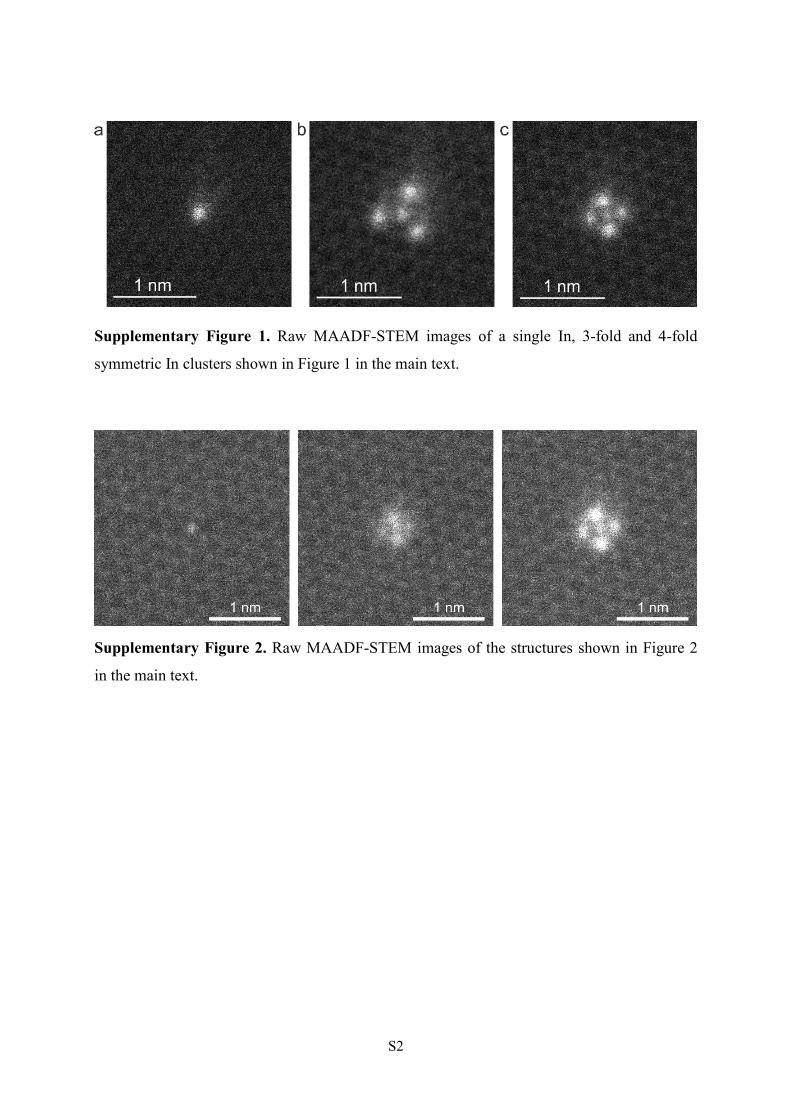
Supplementary Figure 1. Raw MAADF-STEM images of a single In, 3-fold and 4-fold
symmetric In clusters shown in Figure 1 in the main text.
Supplementary Figure 2. Raw MAADF-STEM images of the structures shown in Figure 2
in the main text.
S3
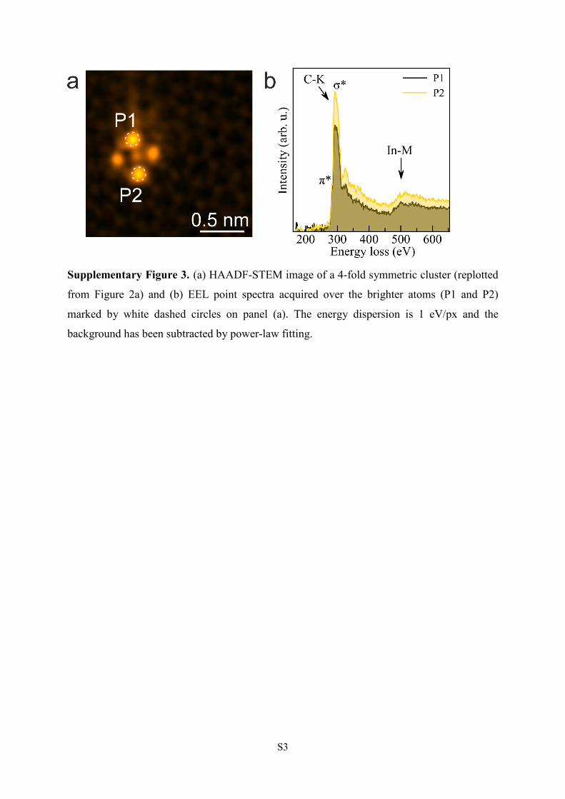
Supplementary Figure 3. (a) HAADF-STEM image of a 4-fold symmetric cluster (replotted
from Figure 2a) and (b) EEL point spectra acquired over the brighter atoms (P1 and P2)
marked by white dashed circles on panel (a). The energy dispersion is 1 eV/px and the
background has been subtracted by power-law fitting.
S4
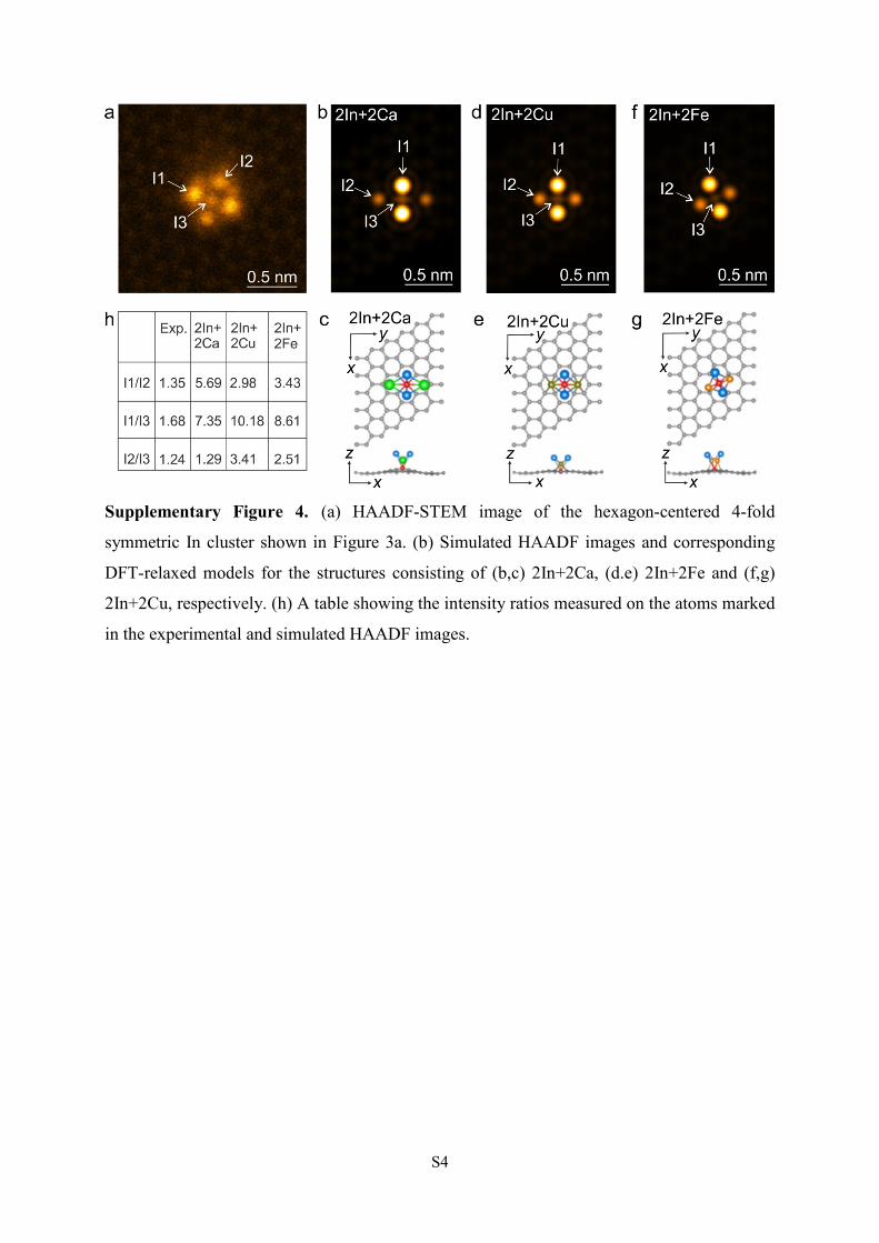
Supplementary Figure 4. (a) HAADF-STEM image of the hexagon-centered 4-fold
symmetric In cluster shown in Figure 3a. (b) Simulated HAADF images and corresponding
DFT-relaxed models for the structures consisting of (b,c) 2In+2Ca, (d.e) 2In+2Fe and (f,g)
2In+2Cu, respectively. (h) A table showing the intensity ratios measured on the atoms marked
in the experimental and simulated HAADF images.
S5
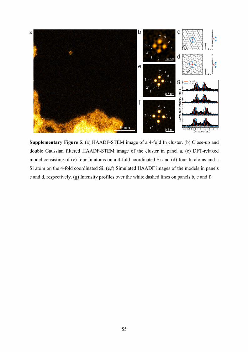
Supplementary Figure 5. (a) HAADF-STEM image of a 4-fold In cluster. (b) Close-up and
double Gaussian filtered HAADF-STEM image of the cluster in panel a. (c) DFT-relaxed
model consisting of (c) four In atoms on a 4-fold coordinated Si and (d) four In atoms and a
Si atom on the 4-fold coordinated Si. (e,f) Simulated HAADF images of the models in panels
c and d, respectively. (g) Intensity profiles over the white dashed lines on panels b, e and f.
S6
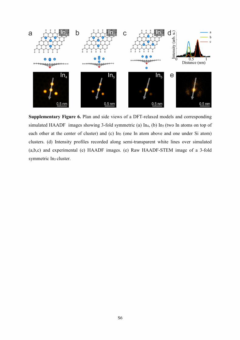
Supplementary Figure 6. Plan and side views of a DFT-relaxed models and corresponding
simulated HAADF images showing 3-fold symmetric (a) In4, (b) In5 (two In atoms on top of
each other at the center of cluster) and (c) In5 (one In atom above and one under Si atom)
clusters. (d) Intensity profiles recorded along semi-transparent white lines over simulated
(a,b,c) and experimental (e) HAADF images. (e) Raw HAADF-STEM image of a 3-fold
symmetric In5 cluster.
S7
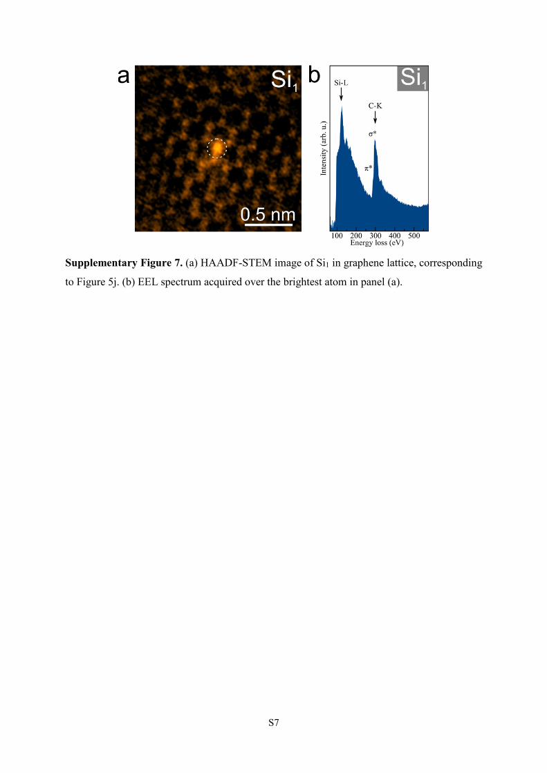
Supplementary Figure 7. (a) HAADF-STEM image of Si1 in graphene lattice, corresponding
to Figure 5j. (b) EEL spectrum acquired over the brightest atom in panel (a).
S8
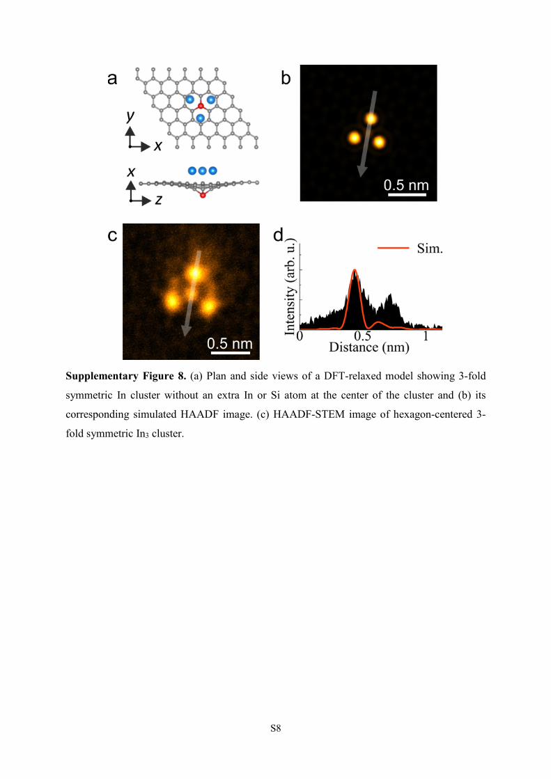
Supplementary Figure 8. (a) Plan and side views of a DFT-relaxed model showing 3-fold
symmetric In cluster without an extra In or Si atom at the center of the cluster and (b) its
corresponding simulated HAADF image. (c) HAADF-STEM image of hexagon-centered 3-
fold symmetric In3 cluster.
S9
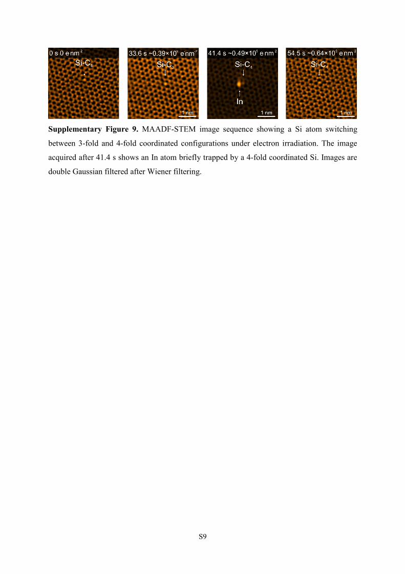
Supplementary Figure 9. MAADF-STEM image sequence showing a Si atom switching
between 3-fold and 4-fold coordinated configurations under electron irradiation. The image
acquired after 41.4 s shows an In atom briefly trapped by a 4-fold coordinated Si. Images are
double Gaussian filtered after Wiener filtering.
S10
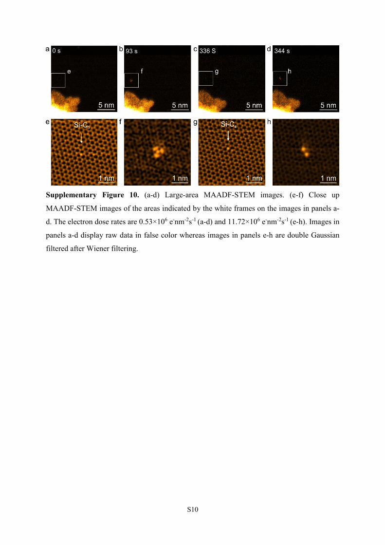
Supplementary Figure 10. (a-d) Large-area MAADF-STEM images. (e-f) Close up
MAADF-STEM images of the areas indicated by the white frames on the images in panels a-
d. The electron dose rates are 0.53×10⁶ e-nm-2s-1 (a-d) and 11.72×10⁶ e-nm-2s-1 (e-h). Images in
panels a-d display raw data in false color whereas images in panels e-h are double Gaussian
filtered after Wiener filtering.
S11
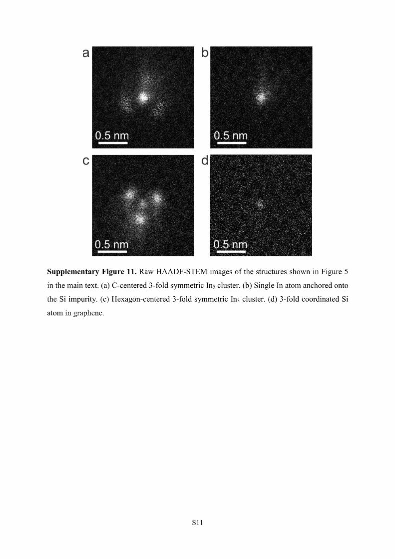
Supplementary Figure 11. Raw HAADF-STEM images of the structures shown in Figure 5
in the main text. (a) C-centered 3-fold symmetric In5 cluster. (b) Single In atom anchored onto
the Si impurity. (c) Hexagon-centered 3-fold symmetric In3 cluster. (d) 3-fold coordinated Si
atom in graphene.
S12
Supplementary Figure 12. MAADF-STEM image sequence of C-centered 3-fold symmetric
In5 cluster shown in Figure 6 in the main text.
S13
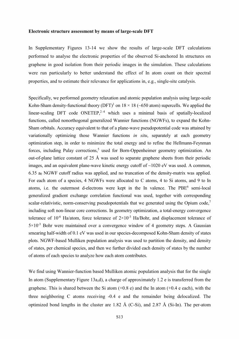
Electronic structure assessment by means of large-scale DFT
In Supplementary Figures 13-14 we show the results of large-scale DFT calculations
performed to analyse the electronic properties of the observed Si-anchored In structures on
graphene in good isolation from their periodic images in the simulation. These calculations
were run particularly to better understand the effect of In atom count on their spectral
properties, and to estimate their relevance for applications in, e.g., single-site catalysis.
Specifically, we performed geometry relaxation and atomic population analysis using large-scale Kohn-Sham density-functional theory (DFT)1 on 18 × 18 (~650 atom) supercells. We applied the linear-scaling DFT code ONETEP,2–4 which uses a minimal basis of spatially-localized functions, called nonorthogonal generalized Wannier functions (NGWFs), to expand the Kohn-Sham orbitals. Accuracy equivalent to that of a plane-wave pseudopotential code was attained by variationally optimizing those Wannier functions in situ, separately at each geometry optimization step, in order to minimize the total energy and to refine the Hellmann-Feynman forces, including Pulay corrections,5 used for Born-Oppenheimer geometry optimization. An out-of-plane lattice constant of 25 Å was used to separate graphene sheets from their periodic images, and an equivalent plane-wave kinetic energy cutoff of ~1020 eV was used. A common, 6.35 a0 NGWF cutoff radius was applied, and no truncation of the density-matrix was applied. For each atom of a species, 4 NGWFs were allocated to C atoms, 4 to Si atoms, and 9 to In atoms, i.e. the outermost d-electrons were kept in the In valence. The PBE6 semi-local generalized gradient exchange correlation functional was used, together with corresponding scalar-relativistic, norm-conserving pseudopotentials that we generated using the Opium code,7 including soft non-linear core corrections. In geometry optimization, a total-energy convergence tolerance of 10-6 Ha/atom, force tolerance of 2×10⁻³ Ha/Bohr, and displacement tolerance of 5×10⁻³ Bohr were maintained over a convergence window of 4 geometry steps. A Gaussian smearing half-width of 0.1 eV was used in our species-decomposed Kohn-Sham density of states plots. NGWF-based Mulliken population analysis was used to partition the density, and density of states, per chemical species, and then we further divided each density of states by the number of atoms of each species to analyze how each atom contributes.
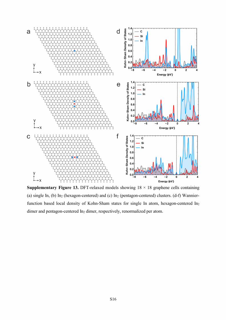
We find using Wannier-function based Mulliken atomic population analysis that for the single
In atom (Supplementary Figure 13a,d), a charge of approximately 1.2 e is transferred from the
graphene. This is shared between the Si atom (+0.8 e) and the In atom (+0.4 e each), with the
three neighboring C atoms receiving -0.4 e and the remainder being delocalized. The
optimized bond lengths in the cluster are 1.82 Å (C-Si), and 2.87 Å (Si-In). The per-atom
S14
Kohn-Sham density of states in this cluster is dominated by near-degenerate In states
distributed around the Fermi level, with further sharp In peaks spread over higher energies.
This suggests that the cluster may serve as an amphoteric but more probably acceptor-like
binding site, and even as a catalytic site, for small molecules.8,9
Referring next to the two In2 dimer configurations (Supplementary Figure 13b,d for hexagon-
centered and 13c,f for pentagon-centered), a larger charge of approximately 2.1 e is
transferred from the graphene. This is shared between the Si atom (+0.9 e) and almost equally
between the two In atoms (+0.6 e each), primarily donated by the 4 nearby C atoms (-0.4 e
each). The optimized bond lengths in the hexagonal-centered cluster are, on average 1.89 Å
(C-Si), 3.04 Å (Si-In), 4.01 Å (In-In). The optimized bond lengths in the pentagon-centered
cluster are, on average 1.90 Å (C-Si), 2.94 Å (Si-In), 3.65 Å (In-In). The per-atom Kohn-
Sham density of states for both of these clusters is characterized by a half-filled four-fold-
degenerate peak at the Fermi level, of predominantly In character. A dense group of In levels
is spread over higher energies.
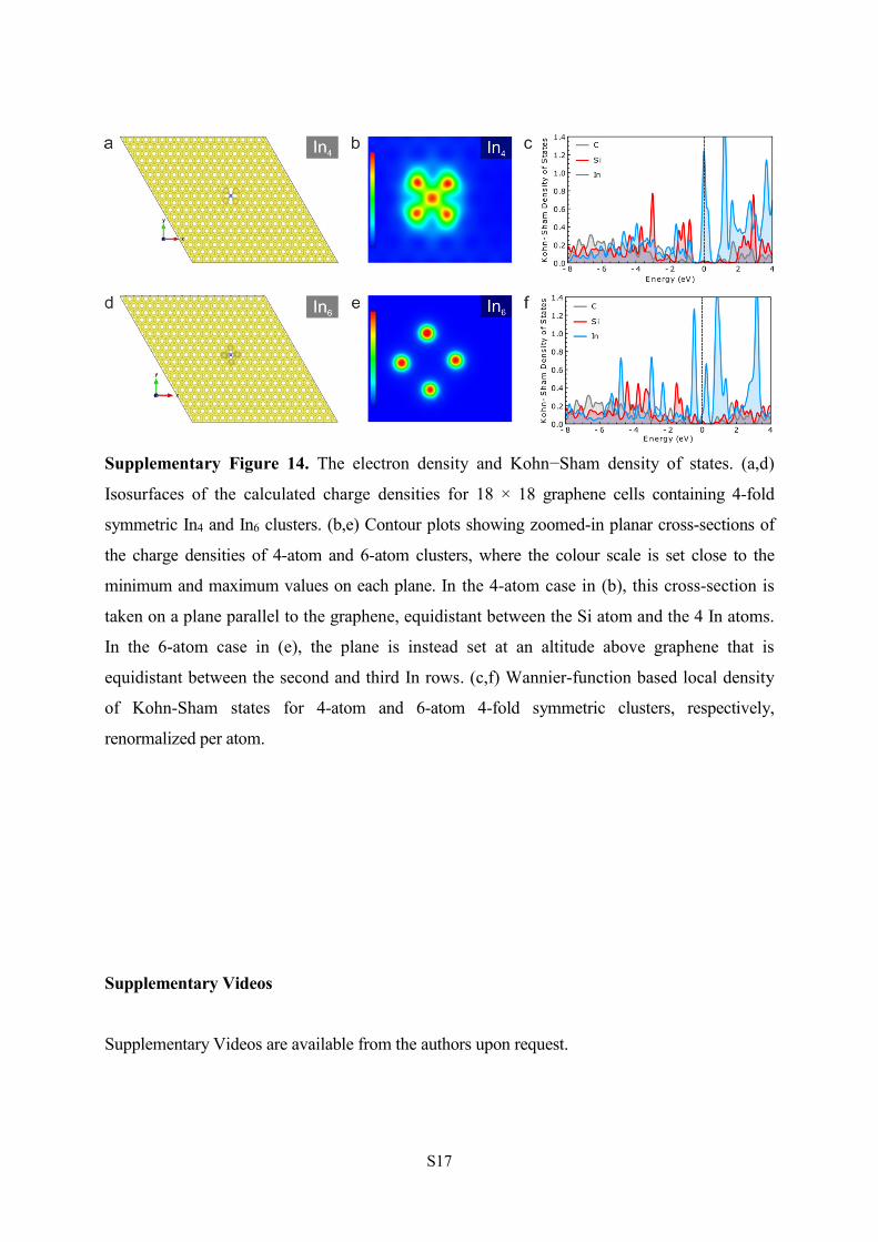
In the In4 cluster (Supplementary Figure 14a-c), a charge of approximately 1.9 e is transferred
from the graphene. This is shared between the Si atom (+0.8 e) and almost equally between
the four In atoms (+0.3 e each), and is primarily donated by 4 nearby C atoms (-0.4 e each).
The optimized bond lengths in the cluster are, on average 1.95 Å (C-Si), 3.30 Å (Si-In), 2.75
Å (In-C), with the In-In bond lengths coming in pairs of length 3.07 Å and 3.14 Å. Amongst
those studied, this cluster exhibits the most prominent partially-filled In peak at the Fermi
level.
Finally, in the In6 cluster (Supplementary Figure 14d-f), approximately 1.7 e is transferred,
but now the only significantly charged atoms are the Si (+0.8 e), the 2 lowest-lying In atoms
adjacent to Si (+0.3 e), and the 4 C atoms bound to Si (-0.3 e). The cluster structure is more
complex, comprising pairs of In atoms at three different altitudes with respect to the graphene
surface, with the atoms in the first and third rows being aligned close to vertically with respect
to each other, above the center of the 5-member C-Si ring. The second row sits above the
center of the 6-member C-Si ring. The intra-row In-In bond length varies, from first to third
row, as 3.24 Å, 4.33 Å, 4.14 Å. The other salient bond lengths are 1.92 Å (C-Si), 3.30 Å (Si-
In), 2.91 Å (Si-In first row), 2.93 Å (In-In first row to third row). The first-row In atoms are
sometimes closer to the C atoms in the 5-member C-Si ring than to the Si atom, at distances
S15
of approximately 2.8-2.9 Å. The per-atom Kohn-Sham density of states in this cluster again
reveals a Fermi density dominated by In states, albeit not as sharply so as in the 4-atom case
and, for a given energy, not equally among the In rows. Again, the charge-transfer to the
cluster from the graphene serves to pin the bottom of the In 5p-like density of states to the
Fermi level, potentially providing overall a relatively spatially-localised but prominent
conduit for further charge transfer and possible associated catalytic activity.10–12
On the basis of these calculations alone it is of course impossible to judge which of these clusters
may provide the best activity and selectivity for a given chemical reaction, if any are indeed
suitable for single-site catalysis. However, we can say that all of them should provide a strongly
polarizing localized environment, and most likely act as electron acceptors, possibly
amphoterically. A range of In-In and In-Si bond lengths are available across the clusters studied,
and shorter bond lengths may suggest greater resistance to catalyst erosion and consumption.
Overall, these clusters present an interesting avenue to extent the concept of the single-atom
catalyst to more complex cluster geometries.
S16
Supplementary Figure 13. DFT-relaxed models showing 18 × 18 graphene cells containing
(a) single In, (b) In2 (hexagon-centered) and (c) In2 (pentagon-centered) clusters. (d-f) Wannier-
function based local density of Kohn-Sham states for single In atom, hexagon-centered In2
dimer and pentagon-centered In2 dimer, respectively, renormalized per atom.
S17
Supplementary Figure 14. The electron density and Kohn−Sham density of states. (a,d)
Isosurfaces of the calculated charge densities for 18 × 18 graphene cells containing 4-fold
symmetric In4 and In6 clusters. (b,e) Contour plots showing zoomed-in planar cross-sections of
the charge densities of 4-atom and 6-atom clusters, where the colour scale is set close to the
minimum and maximum values on each plane. In the 4-atom case in (b), this cross-section is
taken on a plane parallel to the graphene, equidistant between the Si atom and the 4 In atoms.
In the 6-atom case in (e), the plane is instead set at an altitude above graphene that is
equidistant between the second and third In rows. (c,f) Wannier-function based local density
of Kohn-Sham states for 4-atom and 6-atom 4-fold symmetric clusters, respectively,
renormalized per atom.
Supplementary Videos
Supplementary Videos are available from the authors upon request.
S18
Supplementary References
1. Kohn, W. & Sham, L. J. Self-Consistent Equations Including Exchange and Correlation Effects.
Phys. Rev. 140, A1133–A1138 (1965).
2. Skylaris, C.-K., Haynes, P. D., Mostofi, A. A. & Payne, M. C. Introducing ONETEP: Linear-
scaling density functional simulations on parallel computers. J. Chem. Phys. 122, 084119 (2005).
3. Hine, N. D. M. et al. Accurate ionic forces and geometry optimization in linear-scaling density-
functional theory with local orbitals. Phys. Rev. B 83, 195102 (2011).
4. Prentice, J. C. A. et al. The ONETEP linear-scaling density functional theory program. J. Chem.
Phys. 152, 174111 (2020).
5. Ruiz-Serrano, Á., Hine, N. D. M. & Skylaris, C.-K. Pulay forces from localized orbitals optimized
in situ using a psinc basis set. J. Chem. Phys. 136, 234101 (2012).
6. Perdew, J. P., Burke, K. & Ernzerhof, M. Generalized Gradient Approximation Made Simple.
Phys. Rev. Lett. 77, 3865–3868 (1996).
7. Grinberg, I., Ramer, N. J. & Rappe, A. M. Transferable relativistic Dirac-Slater pseudopotentials.
Phys. Rev. B 62, 2311–2314 (2000).
8. Mitchinson, A. & Finkelstein, J. Small-molecule catalysis. Nature 455, 303–303 (2008).
9. Sudheeshkumar, V., Sulaiman, K. O. & Scott, R. W. J. Activation of atom-precise clusters for
catalysis. Nanoscale Adv. 2, 55–69 (2020).
10. Ma, Y. et al. Highly efficient catalytic activity for the hydrogen evolution reaction on pristine and
monovacancy defected WP systems: a first-principles investigation. Phys. Chem. Chem. Phys. 20,
13757–13764 (2018).
11. Vayssilov, G. N. & van Santen, R. A. Catalytic Activity of Titanium Silicalites—a DFT Study.
Journal of Catalysis 175, 170–174 (1998).
12. Zhou, M., Zhang, A., Dai, Z., Zhang, C. & Feng, Y. P. Greatly enhanced adsorption and catalytic
activity of Au and Pt clusters on defective graphene. J. Chem. Phys. 132, 194704 (2010).