Improving Thermal Cycle and Mechanical Drop Impact Resistance of a Lead-free Tin-Silver-Bismuth-Indium Solder Alloy with Minor Doping of Copper Additive Takehiro Wada 1 , Seiji Tsuchiya 1 , Shantanu Joshi 2 , Roberto Garcia 2 , Kimiaki Mori 1 , Takeshi Shirai 1 1 Koki Company Ltd., Japan, 2 Koki Solder America Inc., USA Abstract For a demanding automotive electronics assembly, a highly thermal fatigue resistant solder alloy is required, which makes the lead-free Sn-Ag-Cu type solder alloy unusable. Sn-Ag-Bi-In solder alloy is considered as a high reliability solder alloy due to significant improvement in thermal fatigue resistance as compared to a standard Sn-Ag-Cu alloy. The alloy has not only good thermal fatigue properties but it also has superior ductility and tensile strength by appropriate addition of In; however, initial results indicated a sub-par performance in joint reliability when it is soldered on a printed circuit board (PCB) with Electroless Nickel Immersion Gold (ENIG) surface finish. Numerous experiments were performed to find out appropriate alloying element which would help improve the performance on ENIG PCBs. Sn-Ag-Bi-In solder alloys with and without Cu additions were prepared and then tests were carried out to see the performance in a thermal fatigue test and a drop resistance test.to investigate the impact of Cu addition towards the improvement of joint reliability on ENIG finish PCB. Also, the mechanism of such improvement is documented. Introduction Sn-Ag-Cu type solder alloy has become the standard lead-free solder alloy. There have been a large number of experiments in developing a new generation high reliability alloy for demanding applications. However, a solder alloy which could be used in an extremely demanding application is yet to be determined. Among the new generation alloys Sn-Ag-Bi-In type solder alloys[1,2] have been used as an alloy which shows significant improvement in thermal fatigue resistance, due to appropriate amount of In addition. The improvement in thermal fatigue strength is important as the ductility of the alloy was not sacrificed in the process, which is often the case. When SABI alloy was developed, the initial data suggested significant improvement in the PCBs with Cu-OSP surface finish but there was significant reduction in the performance on PCBs with ENIG surface finish. Numerous experiments were carried out to see if any minor alloying element would help this phenomenon. The results with Cu-OSP board finish suggested that ‘Cu’ helps on strengthening the joint. Taking the same into consideration, different alloys with varying percentage of copper were formulated. Material characterization was performed by preparing dumbbell samples to get the right amount of Cu for the application. . Board level reliability tests were carried out to see the thermal fatigue and drop shock resistance of the alloy. Experimental Solder Alloy Composition and Melting Point Three different solder alloy compositions were prepared for this experiment (Table 1). Table 1: Solder alloy composition and Melting point Alloy No. Composition/wt% Melting Temperature/°C Sn Ag Cu Bi In SA1 (SnAgCu) Bal. 3.0 0.5 - - 217-219 SA2 (SABI) Bal. 3.5 - 0.5 6.0 202-210 SA3 (SABI + Cu) Bal. 3.5 0.8 0.5 6.0 202-206 Since more In which is an element which lowers the melting point, is added to SA2 and SA3, their melting points are lower than SA1. In addition, the melting point of SA3 is lower than SA2, as SA3 contains less than 1wt. % Cu which lowers the melting point. Tensile Test Tensile testing was conducted on the micro-dumbbells as shown in Figure 1. The micro-dumbbells were manufactured by casting molten solder at around 300°C into a die which is preheated to the same temperature. Then the die was immersed in a coolant which was formulated to set the cooling rate around 5K°/second at the time of reaching the solidus temperature, so
Transcript
Improving Thermal Cycle and Mechanical Drop Impact Resistance of a Lead-free
Tin-Silver-Bismuth-Indium Solder Alloy with Minor Doping of Copper Additive
Takehiro Wada1, Seiji Tsuchiya1, Shantanu Joshi2, Roberto Garcia2, Kimiaki Mori1, Takeshi Shirai1 1Koki Company Ltd., Japan, 2Koki Solder America Inc., USA
Abstract
For a demanding automotive electronics assembly, a highly thermal fatigue resistant solder alloy is required, which makes the
lead-free Sn-Ag-Cu type solder alloy unusable. Sn-Ag-Bi-In solder alloy is considered as a high reliability solder alloy due to
significant improvement in thermal fatigue resistance as compared to a standard Sn-Ag-Cu alloy. The alloy has not only good
thermal fatigue properties but it also has superior ductility and tensile strength by appropriate addition of In; however, initial
results indicated a sub-par performance in joint reliability when it is soldered on a printed circuit board (PCB) with
Electroless Nickel Immersion Gold (ENIG) surface finish. Numerous experiments were performed to find out appropriate
alloying element which would help improve the performance on ENIG PCBs. Sn-Ag-Bi-In solder alloys with and without Cu
additions were prepared and then tests were carried out to see the performance in a thermal fatigue test and a drop resistance
test.to investigate the impact of Cu addition towards the improvement of joint reliability on ENIG finish PCB. Also, the
mechanism of such improvement is documented.
Introduction
Sn-Ag-Cu type solder alloy has become the standard lead-free solder alloy. There have been a large number of experiments in
developing a new generation high reliability alloy for demanding applications. However, a solder alloy which could be used
in an extremely demanding application is yet to be determined. Among the new generation alloys Sn-Ag-Bi-In type solder
alloys[1,2] have been used as an alloy which shows significant improvement in thermal fatigue resistance, due to appropriate
amount of In addition. The improvement in thermal fatigue strength is important as the ductility of the alloy was not
sacrificed in the process, which is often the case. When SABI alloy was developed, the initial data suggested significant
improvement in the PCBs with Cu-OSP surface finish but there was significant reduction in the performance on PCBs with
ENIG surface finish. Numerous experiments were carried out to see if any minor alloying element would help this
phenomenon. The results with Cu-OSP board finish suggested that ‘Cu’ helps on strengthening the joint. Taking the same into
consideration, different alloys with varying percentage of copper were formulated. Material characterization was performed
by preparing dumbbell samples to get the right amount of Cu for the application. . Board level reliability tests were carried
out to see the thermal fatigue and drop shock resistance of the alloy.
Experimental
Solder Alloy Composition and Melting Point
Three different solder alloy compositions were prepared for this experiment (Table 1).
Table 1: Solder alloy composition and Melting point
Alloy No. Composition/wt% Melting
Temperature/°C Sn Ag Cu Bi In
SA1
(SnAgCu) Bal. 3.0 0.5 - - 217-219
SA2
(SABI) Bal. 3.5 - 0.5 6.0 202-210
SA3
(SABI + Cu) Bal. 3.5 0.8 0.5 6.0 202-206
Since more In which is an element which lowers the melting point, is added to SA2 and SA3, their melting points are lower
than SA1. In addition, the melting point of SA3 is lower than SA2, as SA3 contains less than 1wt. % Cu which lowers the
melting point.
Tensile Test
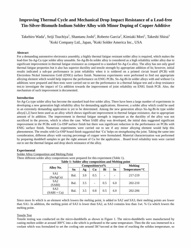
Tensile testing was conducted on the micro-dumbbells as shown in Figure 1. The micro-dumbbells were manufactured by
casting molten solder at around 300°C into a die which is preheated to the same temperature. Then the die was immersed in a
coolant which was formulated to set the cooling rate around 5K°/second at the time of reaching the solidus temperature, so
that the micro-dumbbell would have roughly the same micro-structure as the soldered joints from the SMT process.
Figure 1 - Appearance of Micro-Dumbbell
Micro-dumbbells were divided into 2 groups, namely, as cast and aged. No post-casting treatment was given to the as-cast
group, whereas the aged group was stored at 150°C for 500 hours to compare the thermal resistance. Tensile testing was
conducted by pulling the dumbbell with a constant strain speed of 1.0 x10³s-1, in an air atmosphere at room temperature. The
elongation is measured by the crosshead displacement of the tensile testing machine.
Assembly
The PCBs for this experiment were assembled using solder paste containing Type 4 solder powder of each alloy and no-clean
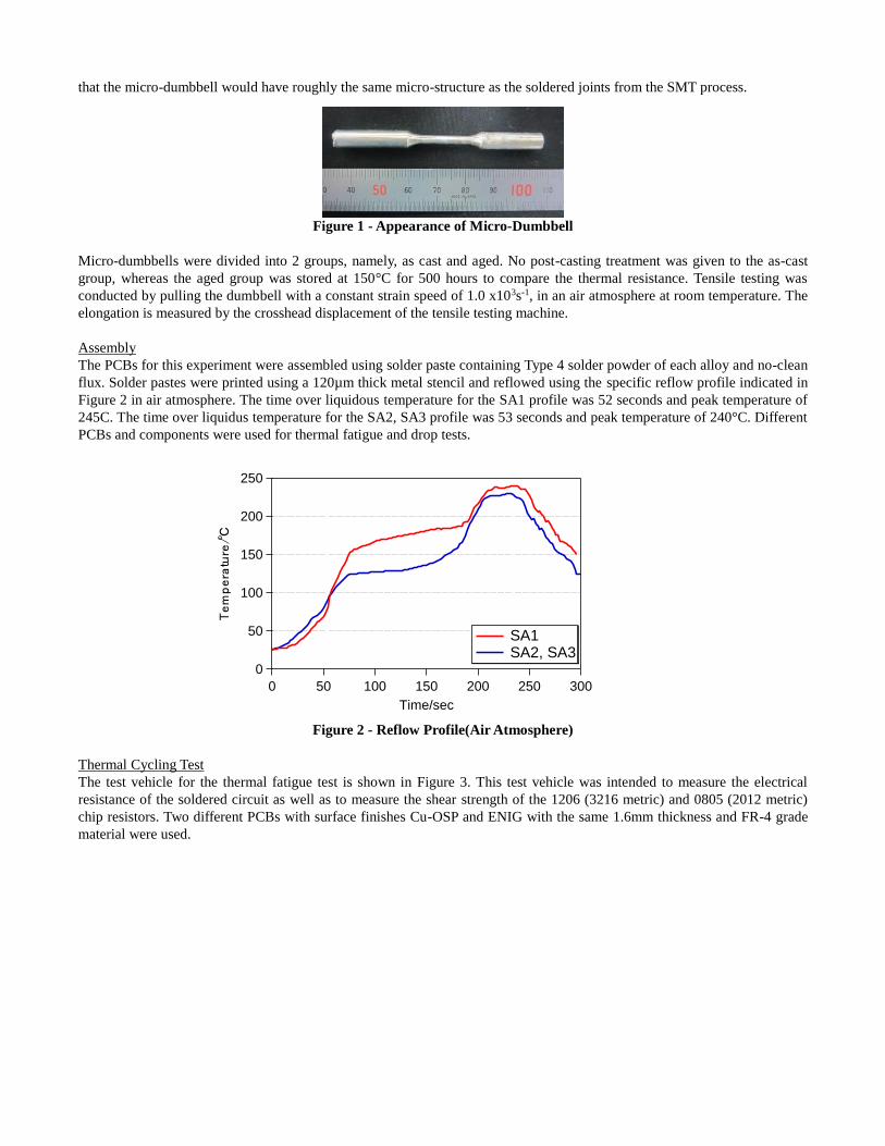
flux. Solder pastes were printed using a 120µm thick metal stencil and reflowed using the specific reflow profile indicated in
Figure 2 in air atmosphere. The time over liquidous temperature for the SA1 profile was 52 seconds and peak temperature of
245C. The time over liquidus temperature for the SA2, SA3 profile was 53 seconds and peak temperature of 240°C. Different
PCBs and components were used for thermal fatigue and drop tests.
Figure 2 - Reflow Profile(Air Atmosphere)
Thermal Cycling Test
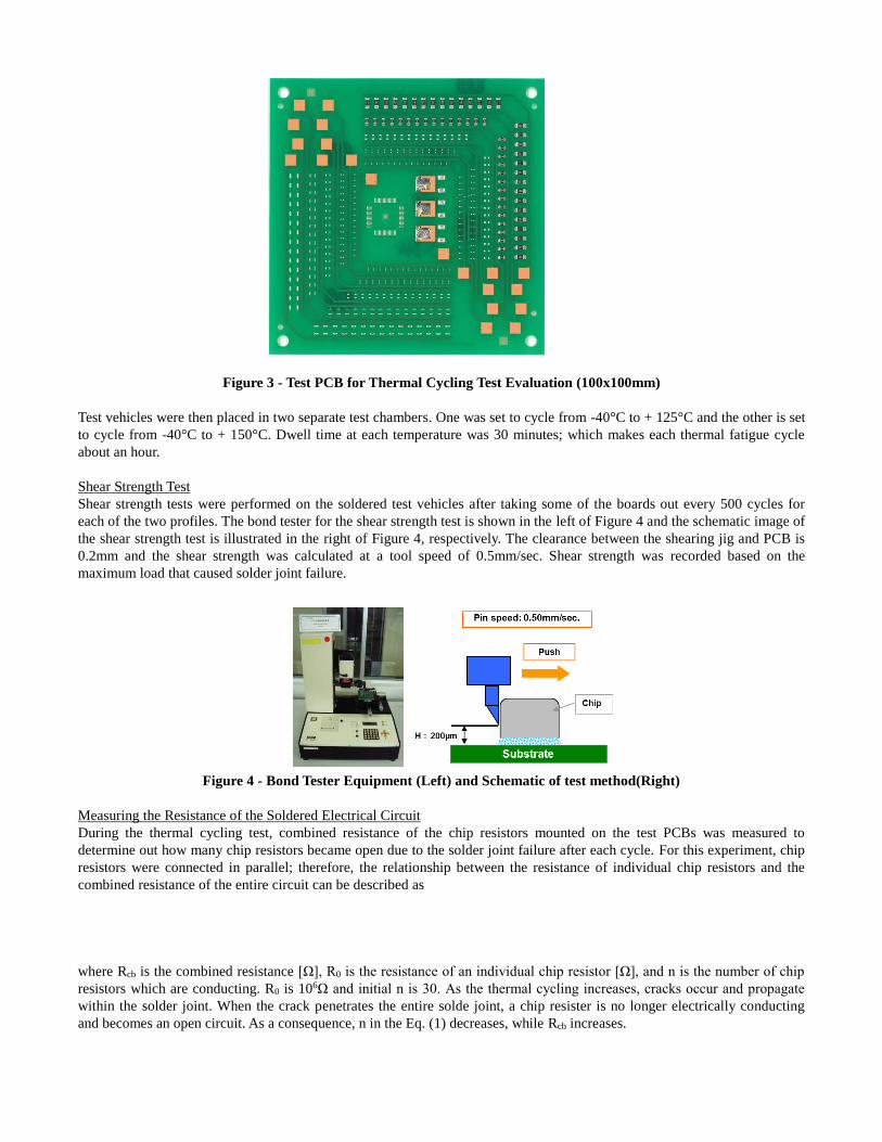
The test vehicle for the thermal fatigue test is shown in Figure 3. This test vehicle was intended to measure the electrical
resistance of the soldered circuit as well as to measure the shear strength of the 1206 (3216 metric) and 0805 (2012 metric)
chip resistors. Two different PCBs with surface finishes Cu-OSP and ENIG with the same 1.6mm thickness and FR-4 grade
material were used.
250
200
150
100
50
0
Tem
pera
ture
/℃
300250200150100500
Time/sec
SA1 SA2, SA3
Figure 3 - Test PCB for Thermal Cycling Test Evaluation (100x100mm)
Test vehicles were then placed in two separate test chambers. One was set to cycle from -40°C to + 125°C and the other is set
to cycle from -40°C to + 150°C. Dwell time at each temperature was 30 minutes; which makes each thermal fatigue cycle
about an hour.
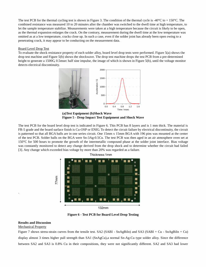
Shear Strength Test
Shear strength tests were performed on the soldered test vehicles after taking some of the boards out every 500 cycles for
each of the two profiles. The bond tester for the shear strength test is shown in the left of Figure 4 and the schematic image of
the shear strength test is illustrated in the right of Figure 4, respectively. The clearance between the shearing jig and PCB is
0.2mm and the shear strength was calculated at a tool speed of 0.5mm/sec. Shear strength was recorded based on the
maximum load that caused solder joint failure.
Figure 4 - Bond Tester Equipment (Left) and Schematic of test method(Right)
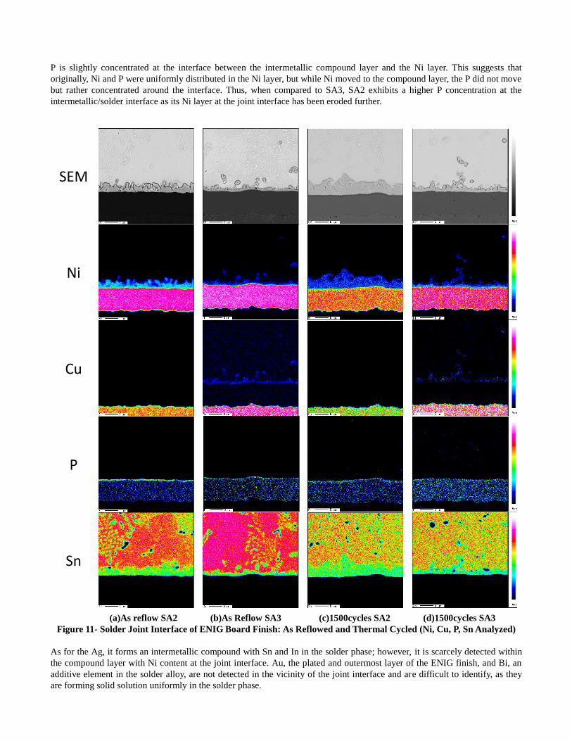
Measuring the Resistance of the Soldered Electrical Circuit
During the thermal cycling test, combined resistance of the chip resistors mounted on the test PCBs was measured to
determine out how many chip resistors became open due to the solder joint failure after each cycle. For this experiment, chip
resistors were connected in parallel; therefore, the relationship between the resistance of individual chip resistors and the
combined resistance of the entire circuit can be described as
where Rcb is the combined resistance [Ω], R0 is the resistance of an individual chip resistor [Ω], and n is the number of chip
resistors which are conducting. R0 is 106Ω and initial n is 30. As the thermal cycling increases, cracks occur and propagate
within the solder joint. When the crack penetrates the entire solde joint, a chip resister is no longer electrically conducting
and becomes an open circuit. As a consequence, n in the Eq. (1) decreases, while Rcb increases.
0 (1)cb
RR
n ・・・・Eq.
The test PCB for the thermal cycling test is shown in Figure 3. The condition of the thermal cycle is -40°C to + 150°C. The
combined resistance was measured 10 to 20 minutes after the chamber was switched to the dwell time at high temperature, to
let the sample temperature stabilize. Measurements were taken at a high temperature because the circuit is likely to be open,
as the thermal expansion enlarges the crack. On the contrary, measurement during the dwell time at the low temperature was
omitted as at a low temperature, cracks close up. In such a case, even if the solder joint has already been open owing to a
penetrating crack, it may appear to be conducting on the measurement data.
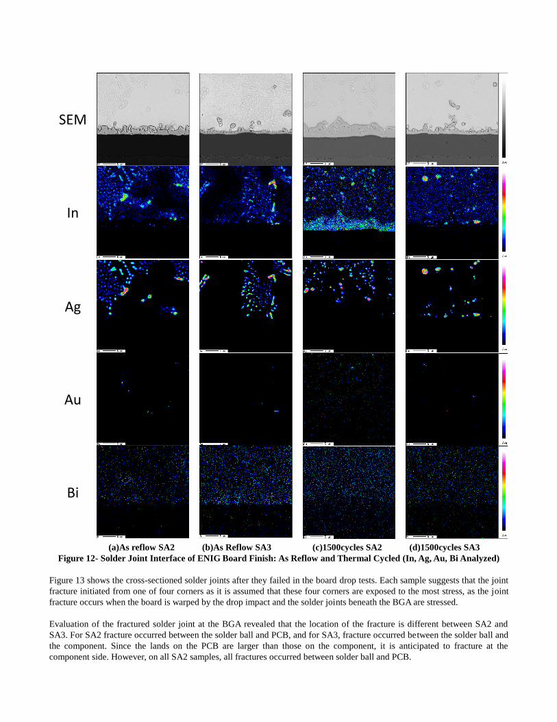
Board Level Drop Test
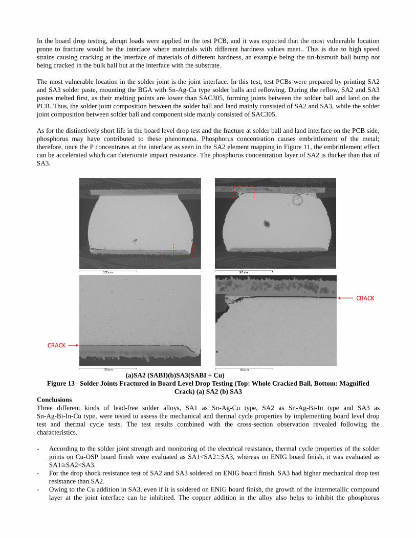
To evaluate the shock resistance property of each solder alloy, board level drop tests were performed. Figure 5(a) shows the
drop test machine and Figure 5(b) shows the shockwave. The drop test machine drops the test PCB from a pre-determined
height to generate a 1500G, 0.5msec half sine impulse, the image of which is shown in Figure 5(b), until the voltage monitor
detects electrical discontinuity.
(a)Test Equipment (b)Shock Wave
Figure 5 - Drop Impact Test Equipment and Shock Wave
The test PCB for the board level drop test is indicated in Figure 6. This PCB has 8 layers and is 1 mm thick. The material is
FR-5 grade and the board surface finish is Cu-OSP or ENIG. To detect the circuit failure by electrical discontinuity, the circuit
is patterned so that all BGA balls are in one series circuit. One 15mm x 15mm BGA with 196 pins was mounted at the center
of the test PCB. Solder balls on the BGA were Sn-3Ag-0.5Cu. The test PCB was then aged in an air atmosphere oven set at
150°C for 500 hours to promote the growth of the intermetallic compound phase at the solder joint interface. Bias voltage
was constantly monitored to detect any change derived from the drop shock and to determine whether the circuit had failed
[3]. Any change which exceeded bias voltage by more than 20% was regarded as a failure.
`
Figure 6 - Test PCB for Board Level Drop Testing
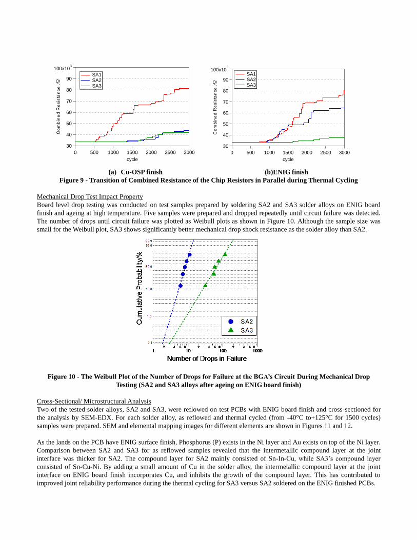
Results and Discussion
Mechanical Property
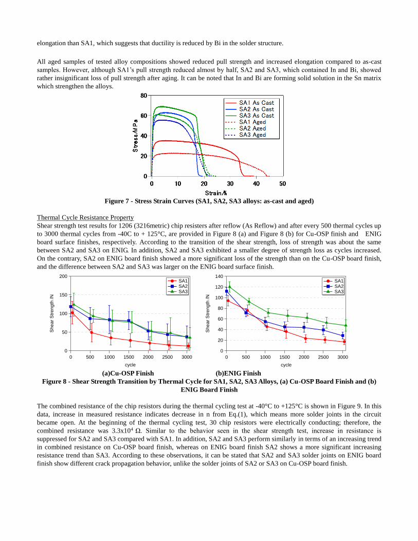
Figure 7 shows stress-strain curves from the tensile test. SA2 (SABI - SnAgBiIn) and SA3 (SABI + Cu - SnAgBiIn + Cu)
display almost 3 times higher pull strength than SA1 (SnAgCu),a normal Sn-Ag-Cu type solder alloy. Since the difference
between SA2 and SA3 is 0.8% Cu in their compositions, they were not significantly different. SA2 and SA3 had lower
2000
1500
1000
500
0
Accele
ration / G
1.61.20.80.40.0
Time / msec
elongation than SA1, which suggests that ductility is reduced by Bi in the solder structure.
All aged samples of tested alloy compositions showed reduced pull strength and increased elongation compared to as-cast
samples. However, although SA1’s pull strength reduced almost by half, SA2 and SA3, which contained In and Bi, showed
rather insignificant loss of pull strength after aging. It can be noted that In and Bi are forming solid solution in the Sn matrix
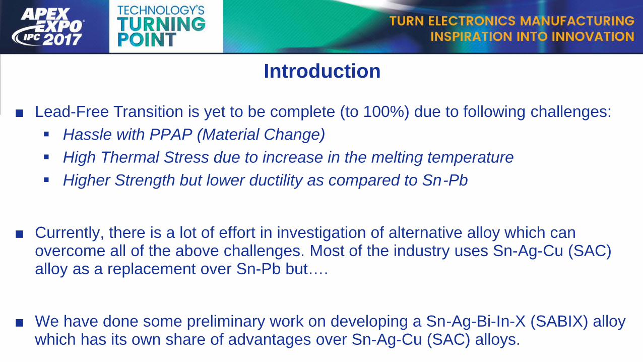
■ Lead-Free Transition is yet to be complete (to 100%) due to following challenges:
Hassle with PPAP (Material Change) High Thermal Stress due to increase in the melting temperature Higher Strength but lower ductility as compared to Sn-Pb
■ Currently, there is a lot of effort in investigation of alternative alloy which can overcome all of the above challenges. Most of the industry uses Sn-Ag-Cu (SAC) alloy as a replacement over Sn-Pb but….
■ We have done some preliminary work on developing a Sn-Ag-Bi-In-X (SABIX) alloy which has its own share of advantages over Sn-Ag-Cu (SAC) alloys.
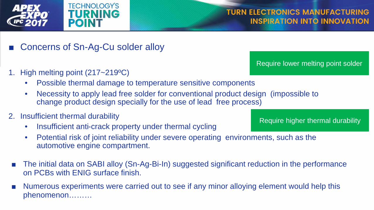
■ Concerns of Sn-Ag-Cu solder alloy
1. High melting point (217~219ºC)
• Possible thermal damage to temperature sensitive components
• Necessity to apply lead free solder for conventional product design (impossible to change product design specially for the use of lead free process)
2. Insufficient thermal durability
• Insufficient anti-crack property under thermal cycling
• Potential risk of joint reliability under severe operating environments, such as the automotive engine compartment.
Require lower melting point solder
Require higher thermal durability
■ The initial data on SABI alloy (Sn-Ag-Bi-In) suggested significant reduction in the performance on PCBs with ENIG surface finish.
■ Numerous experiments were carried out to see if any minor alloying element would help this phenomenon………
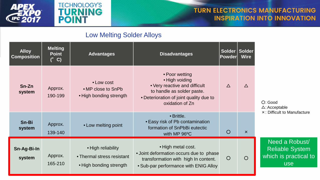
Low Melting Solder Alloys
Alloy
Composition
Melting
Point
(°C)
Advantages DisadvantagesSolder
Powder
Solder
Wire
Sn-Zn
systemApprox.
190-199
• Low cost
• MP close to SnPb
• High bonding strength
• Poor wetting
• High voiding
• Very reactive and difficult
to handle as solder paste.
• Deterioration of joint quality due to
oxidation of Zn
△ △
Sn-Bi
systemApprox.
139-140
• Low melting point
• Brittle.
• Easy risk of Pb contamination
formation of SnPbBi eutectic
with MP 96ºC ○ ×
Sn-Ag-Bi-In
system Approx.
165-210
• High reliability
• Thermal stress resistant
• High bonding strength
• High metal cost.
• Joint deformation occurs due to phase
transformation with high In content.
• Sub-par performance with ENIG Alloy
○ ○
○: Good
△: Acceptable
×: Difficult to Manufacture
Need a Robust/
Reliable System
which is practical to
use
Minor Alloying (Cu)
■ The results with Cu-OSP board finish suggested that ‘Cu’ helps on strengthening the joint.
■ Taking the same into consideration, different alloys with varying percentage of copper were formulated.
■ Material characterization was performed by preparing dumbbell samples to get the right amount of Cu for the application.
■ Board level reliability tests were carried out to see the thermal fatigue and drop shock resistance of the alloy.
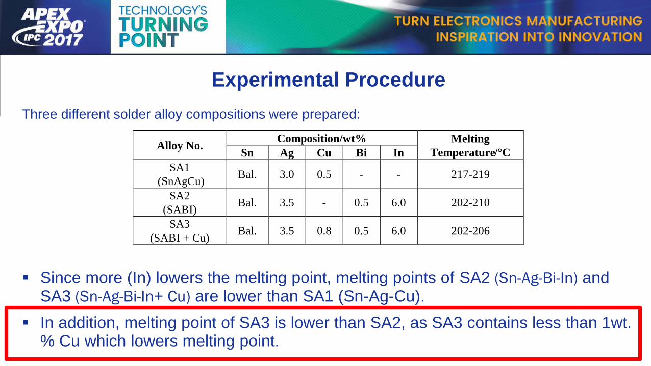
Experimental Procedure
Three different solder alloy compositions were prepared:
Alloy No. Composition/wt% Melting Temperature/°C Sn Ag Cu Bi In
SA1 (SnAgCu) Bal. 3.0 0.5 - - 217-219
SA2 (SABI) Bal. 3.5 - 0.5 6.0 202-210
SA3 (SABI + Cu) Bal. 3.5 0.8 0.5 6.0 202-206
Since more (In) lowers the melting point, melting points of SA2 (Sn-Ag-Bi-In) and SA3 (Sn-Ag-Bi-In+ Cu) are lower than SA1 (Sn-Ag-Cu).
In addition, melting point of SA3 is lower than SA2, as SA3 contains less than 1wt. % Cu which lowers melting point.
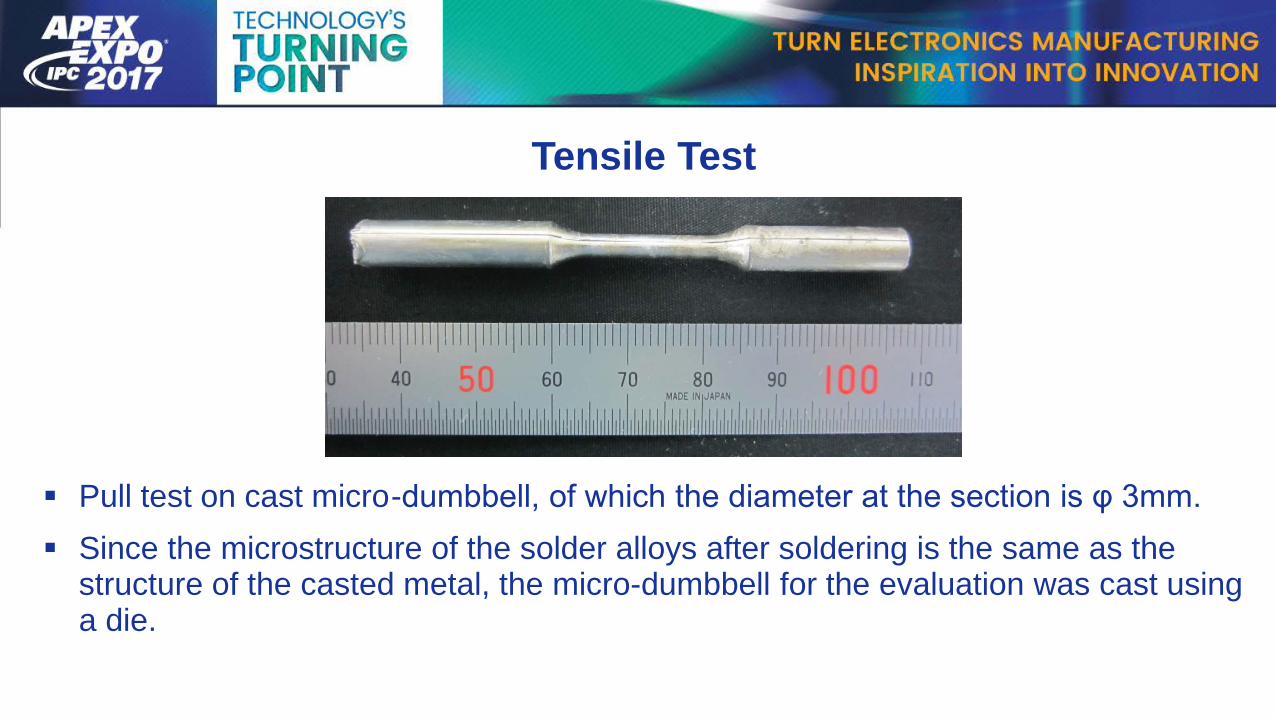
Tensile Test
Pull test on cast micro-dumbbell, of which the diameter at the section is φ 3mm. Since the microstructure of the solder alloys after soldering is the same as the
structure of the casted metal, the micro-dumbbell for the evaluation was cast using a die.
Tensile Test
To obtain equivalent microstructure as the actual solder joint, molten alloys were casted into a die preheated at 573K (300°C).
Then the filled die is cooled down in a cooling solution which is formulated to obtain the same cooling rate as actual soldering process, about 5K/s
Observation on the cross section at the gauge marks of the prepared dumbbell revealed uniform microstructure as intended.
Test Parameters:
• Room Temp
• Strain Rate: 1.0×10⁻³ /s
• Stopped when dumbbell
breaks
Casted micro-dumbbells are
divided into 2 groups:
• As Cast
• Aged 423K
(150°C) for 1000 Hours
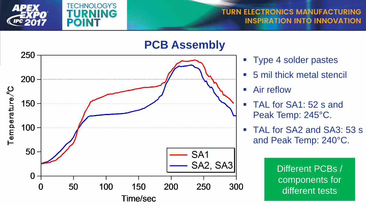
PCB Assembly
Type 4 solder pastes
5 mil thick metal stencil
Air reflow
TAL for SA1: 52 s and Peak Temp: 245°C.
TAL for SA2 and SA3: 53 s and Peak Temp: 240°C.
Different PCBs /
components for
different tests
Thermal Cycling Test
1.6mm thickness and FR-4
1206 (3216 metric) and 0805 (2012 metric) chip resistors.
Two different PCBs:
Cu-OSP and
ENIG
Two different thermal cycles:
-40C to + 125°C
-40C to + 150°C
30 min dwell at each extreme.
Test PCB for Thermal Cycling Test Evaluation(100x100mm)
Same PCB also
used for shear
strength testing
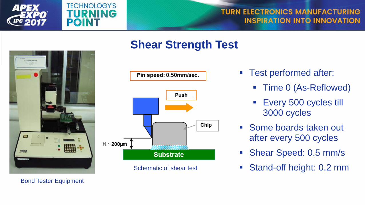
Shear Strength Test
Test performed after:
Time 0 (As-Reflowed)
Every 500 cycles till 3000 cycles
Some boards taken out after every 500 cycles
Shear Speed: 0.5 mm/s
Stand-off height: 0.2 mmSchematic of shear test
Bond Tester Equipment
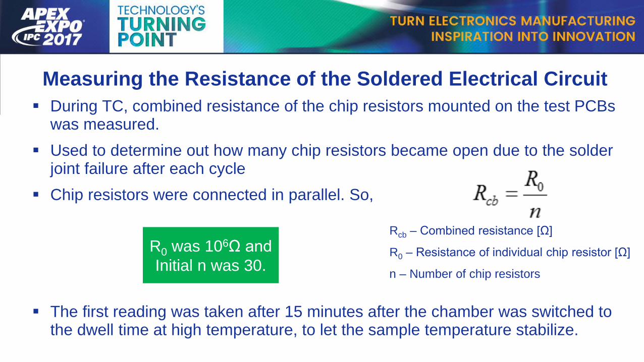
Measuring the Resistance of the Soldered Electrical Circuit
During TC, combined resistance of the chip resistors mounted on the test PCBs was measured.
Used to determine out how many chip resistors became open due to the solder joint failure after each cycle
Chip resistors were connected in parallel. So,
Rcb – Combined resistance [Ω]
R0 – Resistance of individual chip resistor [Ω]
n – Number of chip resistors
R0 was 106Ω and Initial n was 30.
The first reading was taken after 15 minutes after the chamber was switched to the dwell time at high temperature, to let the sample temperature stabilize.
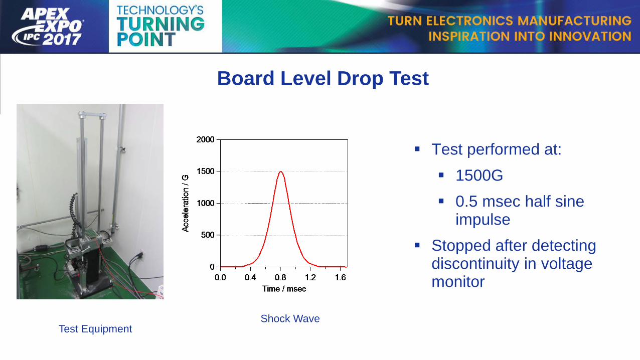
Board Level Drop Test
Test EquipmentShock Wave
Test performed at:
1500G
0.5 msec half sine impulse
Stopped after detecting discontinuity in voltage monitor
Board Level Drop Test
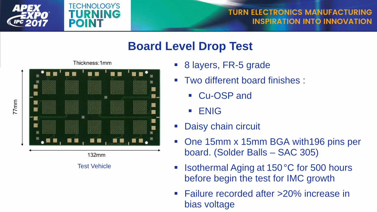
Test Vehicle
8 layers, FR-5 grade
Two different board finishes :
Cu-OSP and
ENIG
Daisy chain circuit
One 15mm x 15mm BGA with196 pins per board. (Solder Balls – SAC 305)
Isothermal Aging at 150°C for 500 hours before begin the test for IMC growth
Failure recorded after >20% increase in bias voltage
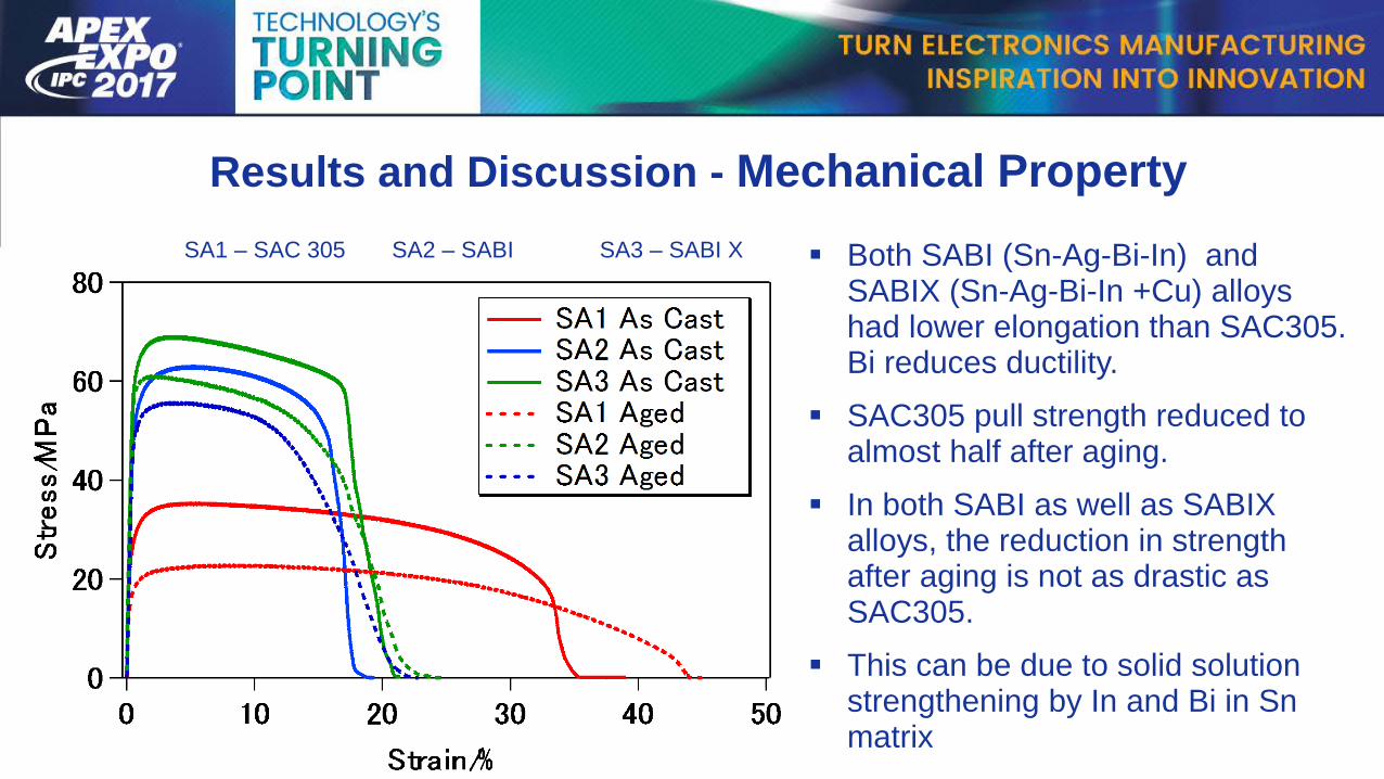
Results and Discussion - Mechanical Property
Both SABI (Sn-Ag-Bi-In) and SABIX (Sn-Ag-Bi-In +Cu) alloys had lower elongation than SAC305. Bi reduces ductility.
SAC305 pull strength reduced to almost half after aging.
In both SABI as well as SABIX alloys, the reduction in strength after aging is not as drastic as SAC305.
This can be due to solid solution strengthening by In and Bi in Sn matrix
SA1 – SAC 305 SA2 – SABI SA3 – SABI X
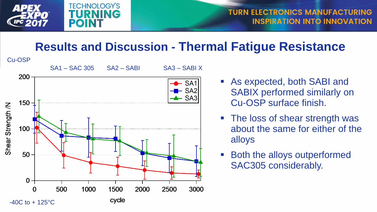
Results and Discussion - Thermal Fatigue Resistance
As expected, both SABI and SABIX performed similarly on Cu-OSP surface finish.
The loss of shear strength was about the same for either of the alloys
Both the alloys outperformed SAC305 considerably.
SA1 – SAC 305 SA2 – SABI SA3 – SABI X
Cu-OSP
-40C to + 125°C
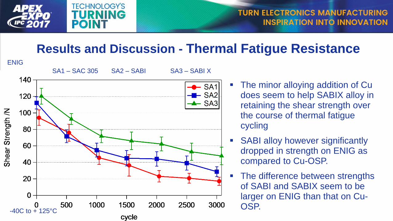
Results and Discussion - Thermal Fatigue Resistance
The minor alloying addition of Cu does seem to help SABIX alloy in retaining the shear strength over the course of thermal fatigue cycling
SABI alloy however significantly dropped in strength on ENIG as compared to Cu-OSP.
The difference between strengths of SABI and SABIX seem to be larger on ENIG than that on Cu-OSP.
SA1 – SAC 305 SA2 – SABI SA3 – SABI X
ENIG
-40C to + 125°C
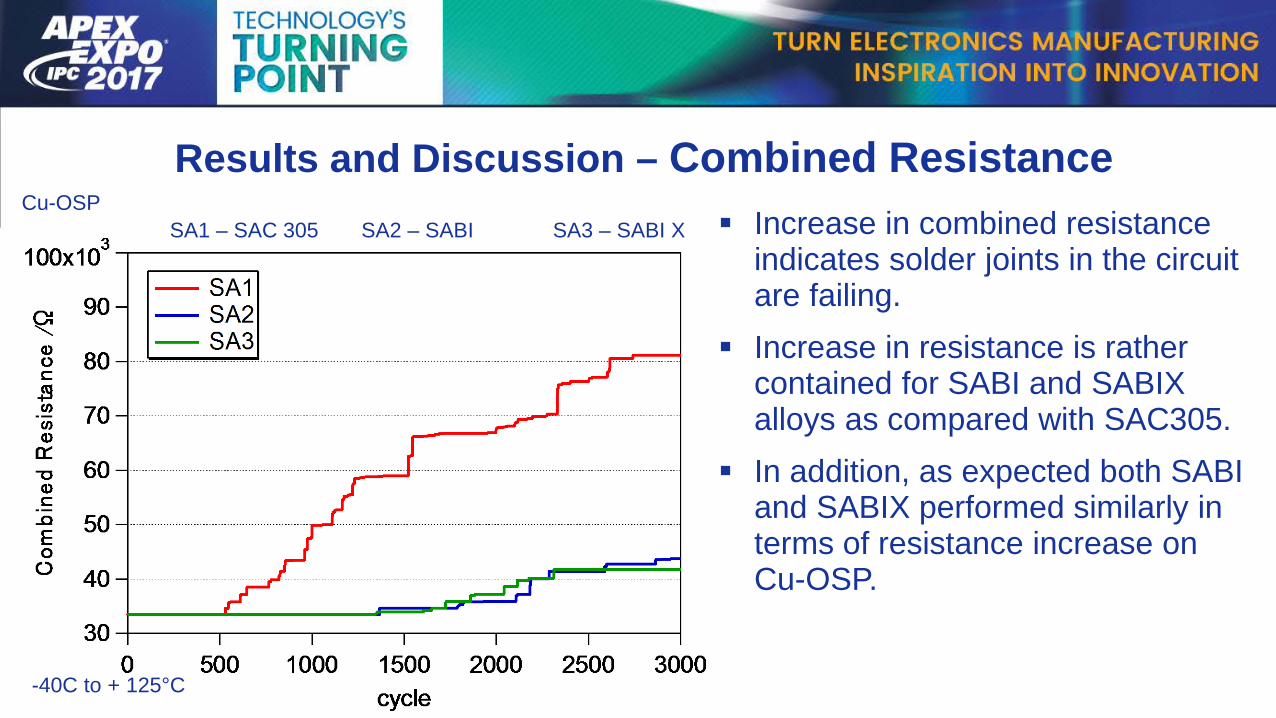
Results and Discussion – Combined Resistance
Increase in combined resistance indicates solder joints in the circuit are failing.
Increase in resistance is rather contained for SABI and SABIX alloys as compared with SAC305.
In addition, as expected both SABI and SABIX performed similarly in terms of resistance increase on Cu-OSP.
SA1 – SAC 305 SA2 – SABI SA3 – SABI X
Cu-OSP
-40C to + 125°C
SA1 – SAC 305 SA2 – SABI SA3 – SABI X
ENIG
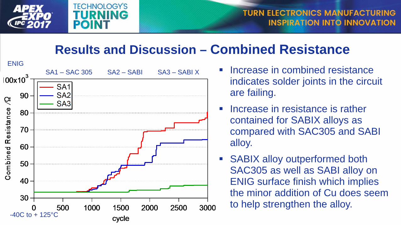
Results and Discussion – Combined Resistance
Increase in combined resistance indicates solder joints in the circuit are failing.
Increase in resistance is rather contained for SABIX alloys as compared with SAC305 and SABI alloy.
SABIX alloy outperformed both SAC305 as well as SABI alloy on ENIG surface finish which implies the minor addition of Cu does seem to help strengthen the alloy.
-40C to + 125°C
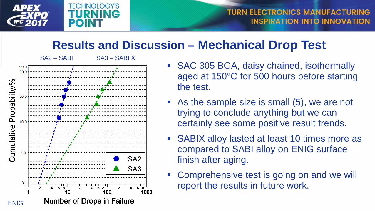
Results and Discussion – Mechanical Drop Test
SAC 305 BGA, daisy chained, isothermally aged at 150°C for 500 hours before starting the test.
As the sample size is small (5), we are not trying to conclude anything but we can certainly see some positive result trends.
SABIX alloy lasted at least 10 times more as compared to SABI alloy on ENIG surface finish after aging.
Comprehensive test is going on and we will report the results in future work.
SA2 – SABI SA3 – SABI X
ENIG
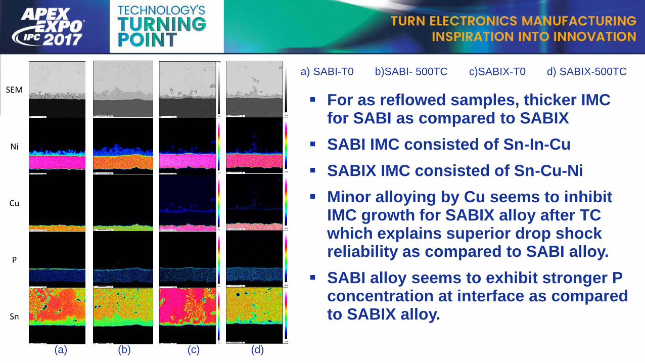
SEM
Ni
Cu
P
Sn
(a) (b) (c) (d)
For as reflowed samples, thicker IMC for SABI as compared to SABIX
SABI IMC consisted of Sn-In-Cu
SABIX IMC consisted of Sn-Cu-Ni
Minor alloying by Cu seems to inhibit IMC growth for SABIX alloy after TC which explains superior drop shock reliability as compared to SABI alloy.
SABI alloy seems to exhibit stronger P concentration at interface as compared to SABIX alloy.
a) SABI-T0 b)SABI- 500TC c)SABIX-T0 d) SABIX-500TC
a b
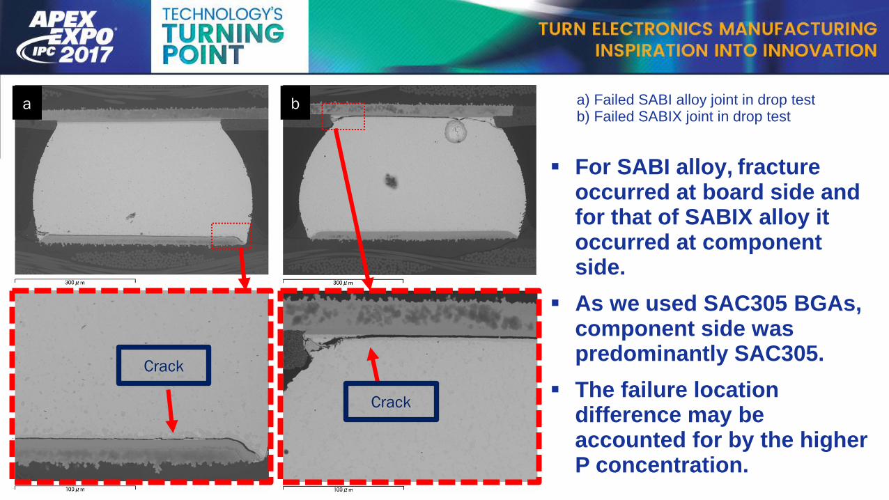
For SABI alloy, fracture occurred at board side and for that of SABIX alloy it occurred at component side.
As we used SAC305 BGAs, component side was predominantly SAC305.
The failure location difference may be accounted for by the higher P concentration.
a) Failed SABI alloy joint in drop test b) Failed SABIX joint in drop test
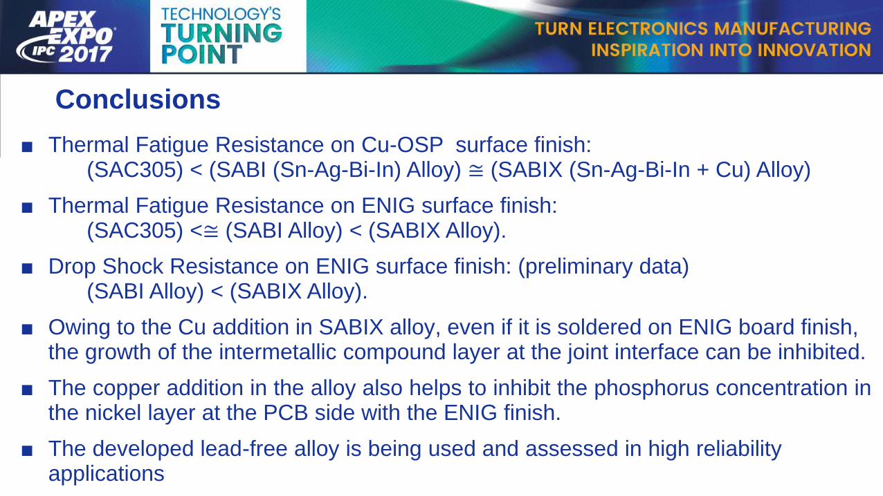
■ Drop Shock Resistance on ENIG surface finish: (preliminary data)(SABI Alloy) < (SABIX Alloy).
■ Owing to the Cu addition in SABIX alloy, even if it is soldered on ENIG board finish, the growth of the intermetallic compound layer at the joint interface can be inhibited.
■ The copper addition in the alloy also helps to inhibit the phosphorus concentration in the nickel layer at the PCB side with the ENIG finish.
■ The developed lead-free alloy is being used and assessed in high reliability applications
Acknowledgements
Co-Authors:
■ Takehiro Wada
■ Seiji Tsuchiya
■ Kimiaki Mori
■ Takeshi Shirai
■ Roberto Garcia Segura
The material is a joint development solder alloy between the company and Panasonic