Indium Phosphide based Integrated Photonic Devices for Telecommunications and Sensing Applications by Ta-Ming Shih M.S. Electrical Engineering Massachusetts Institute of Technology 2007 B.S. Electrical Engineering and Computer Science University of California, Berkeley 2006 Submitted to the Department of Electrical Engineering and Computer Science in partial fulfillment of the requirements for the degree of Doctor of Philosophy in Electrical Engineering at the MASSACHUSETTS INSTITUTE OF TECHNOLOGY June 2012 c 2012 Massachusetts Institute of Technology. All rights reserved. Author .............................................................. Department of Electrical Engineering and Computer Science May 18, 2012 Certified by .......................................................... Leslie A. Kolodziejski Professor of Electrical Engineering Thesis Supervisor Accepted by ......................................................... Leslie A. Kolodziejski Chair, Committee on Graduate Students
Transcript
Indium Phosphide based Integrated Photonic
Devices for Telecommunications and Sensing
Applications
by
Ta-Ming Shih
M.S. Electrical EngineeringMassachusetts Institute of Technology 2007
B.S. Electrical Engineering and Computer ScienceUniversity of California, Berkeley 2006
Submitted to the Department of Electrical Engineering and ComputerScience in partial fulfillment of the requirements for the degree of
Indium Phosphide based Integrated Photonic Devices for
Telecommunications and Sensing Applications
by
Ta-Ming Shih
Submitted to the Department of Electrical Engineering and Computer Scienceon May 18, 2012, in partial fulfillment of the
requirements for the degree ofDoctor of Philosophy in Electrical Engineering
Abstract
Photonics is an exciting area of study that is situated at the cross-section of physics,material science, and electrical engineering. The integration of photonic devicesserves to reduce the size, weight, power consumption, and cost of the photonics-based systems, whose applications can be as disparate in nature as communicationsand medicine. In particular, an integrated all-optical logic gate and wavelength con-verter for fiber-optic telecommunications and an integrated tunable laser for trace-gassensing are investigated in this thesis. These devices are fabricated in the indium phos-phide (InP) material system, which includes InP and the ternary/quaternary III-Vsemiconductors that can be grown closely lattice-matched on the InP substrate.
The all-optical logic gate is designed as a Mach-Zehnder interferometer with semi-conductor optical amplifiers as active nonlinear elements that are optically coupled tothe passive waveguides using the asymmetric twin waveguide technique. The deviceis grown and fabricated monolithically and carrier-dependent optical interference isdemonstrated at the 1.55 µm wavelength. The tunable diode laser is designed to oper-ate in the wavelength range of 1.55 µm – 2 µm for trace-gas spectroscopic sensing andcomprises of strained InGaAs quantum wells. The laser is monolithically fabricatedusing mask-less lithography techniques and tuning is demonstrated in Fabry-Perotcavity lasers under continuous-wave operation. A ring-coupled 2 µm wavelength laseris designed that will exhibit a tuning range of tens of nanometers.
Thesis Supervisor: Leslie A. KolodziejskiTitle: Professor of Electrical Engineering
3
4
Acknowledgments
I am honored to have had the opportunity to work with and learn from so many
talented people during the course of my PhD. It has been an unforgettable experience
that I will cherish for the rest of my life. My wonderful time could not have been
possible without all of the people I worked with at MIT.
I am extremely grateful to my advisor, Professor Leslie Kolodziejski, for all of her
guidance throughout the years. Leslie gave me the freedom to chart my own way,
while she provided a light for the path. She has taught me the value of teamwork
and collaboration, along with the importance of patience. Through all of the ups
and downs of the past 6 years, Leslie has demonstrated to me what it means to stay
focused on the big picture and smile through it all. And finally, she has shown me
how to have fun: I will always remember the parties at her house, at MIT, and even
aboard the Spirit of Boston!
The great thing about being a graduate student in the Integrated Photonic Devices
and Materials group is that one automatically gets to have another advisor: Dr. Gale
Petrich. Gale has always been there to help me get to the bottom of anything that
was suspicious, broken, or missing. I cannot count the number of times that I knocked
on his door with a random question that I knew only he would know. I am thankful
to Gale for all of the explanations, advice, and rides to Lincoln Laboratory!
I would like to express my sincere gratitude toward my committee members, Pro-
fessors Erich Ippen and Rajeev Ram, for their valuable insights and generous guid-
ance. Professor Ippen has been a great source of knowledge and advice since I started
my studies at MIT. He has always been more than happy to make time for any ques-
tions that I had. Rajeev has been a role model for me throughout my PhD. Having
taken two of his classes and helped to TA another, I have a lot of respect for his
modesty and charisma. The people in the groups of Professors Ippen and Ram have
been wonderful to collaborate with, especially Dr. Marcus Dahlem (now Professor),
Dr. Ali Motamedi, Dr. Jason Orcutt, and Dr. Joseph Summers.
Professor Jaime Viegas has become a true mentor and friend during his stay at
5
MIT and the continued collaboration between our group at MIT and his at the Masdar
Institute of Science and Technology. Jaime’s humor has never failed to lighten the
mood of a meeting, and his candor is something that I admire. I want to thank him
for all of the times he sat down with me to help me with my research.
No amount of thanks would be enough to give to the folks at the Nanostructures
Laboratory (NSL) for all of their help and advice. Professor Henry Smith has always
been able to set aside time for me to meet with him. Mark Mondol has been extremely
patient with me as I tried my best not to break the e-beam lithography tool. Dr.
Tim Savas has never failed to put a smile on my face with his humor. A medal of
honor should go to James Daley, who has always been there to answer questions, fix
equipment, perform evaporations, or just talk to in the cleanroom. Jim has been a
mentor in the lab and has become a good friend.
Similarly I need to offer my appreciation to the people at the Microsystems Tech-
nology Laboratories (MTL), where a large fraction of my fabrication work was per-
formed. I want to thank Vicky Diadiuk for her understanding and all of the technical
staff for their patient instruction. Finally, I want to offer a warm “Thank you” to
Debroah Hodges-Pabon for giving me the opportunity to work as a session chair for
the Microsystems Annual Research Conference.
The Integrated Photonics Initiative has been a great joint effort between the
MIT campus and Lincoln Laboratory. The wonderful people at Lincoln have been a
matchless source of guidance and encouragement. It has been tremendous to have
had the opportunity to work with Dr. Paul Juodawlkis, Dr. Reuel Swint, Dr. Jade
Wang, and William Loh. Infinite thanks to Jason Plant for all of the fabrication
assistance and wisdom that he has imparted on me.
I also need to thank all of the staff from 6.007 who have made my two semesters
as TA and one semester as instructor some of the best experiences I had at MIT.
Thank you to Professor James Kirtley and Dr. Yu Gu (now Professor) for being so
supportive. Thank you to Professor Kenneth Wong for trusting me and inviting me
to Hong Kong, and for treating me as a friend. And a million thanks to Professor
Vladimir Bulovic, for his encouragement and counsel throughout it all, and for giving
6
me the opportunity to lecture as a graduate student. His humble attitude toward
teaching will stick with me for the entirety of my career.
I want to thank Orit Shamir, with whom I shared an office for 5 years, for being
such a great friend and colleague. From the gumball trophy, to the taped-shut mini-
fridge, to the carpet-less floor, Orit and I have really made 36-295 an office to call our
own. She has been a great person to discuss ideas with, not all of which pertained
to research. I will always remember the April fool’s day of 2008 when we hacked our
group’s website and replaced it with “Leslie’s Daily Journal,” and our never-published
research paper, “Analysis of Optimized and Quantized Performance and the Results
Obtained.”
It has been a true pleasure to work with Dr. Sheila Nabanja, a fellow groupmate
and next door neighbor. The long days that we spent upstairs in the optics lab as we
took pages of data were tolerable because of her optimism and humor. I also need to
express my gratitude for her shared interest of taking exercise classes at the gym!
During the IAPs of 2009 and 2010 I organized a three-unit seminar class called
“Hooked on Photonics” for MIT undergrads. I want to thank everyone who parti-
cipated for their selflessness and enthusiasm, especially Dr. Vanessa Wood (now
Professor), Dr. Tim Heidel, and Dr. Zheng Wang (now Professor). Course 6.095
could not have been possible without you.
There are many other friends at MIT whom I will not be able to mention here.
But I absolutely need to express my gratitude to everyone in my group for their
fellowship: Pei Chun Amy Chi, Mohammad Araghchini, Dr. Ryan Williams, and Dr.
Reginald Bryant. My experience at MIT would not have been the same without the
kindness from my friends Adrian YiXiang Yeng, Dr. Sidney Tsai, Allen Hsu, David
He, Dr. Amil Patel, Dr. Donald Winston, and Dr. Mahmut Ersin Sinangil.
Finally, I want to thank my family for always being there for me. My parents
have been unrelentingly supportive of my education, applying just the right amount
of pressure here and there to help me along the way. A special thanks goes to my
sister, Hui-Wen, who has been a blessing in my life. And words cannot describe the
gratitude I have for my wife Angela, who, starting from day one has been behind my
7
graduate goals one hundred percent.
Cambridge, 2012 TM S
8
Contents
1 Introduction 21
1.1 The Indium Phosphide Material System . . . . . . . . . . . . . . . . 23
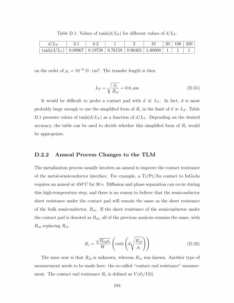
D.1 Values of tanh(d/LT ) for different values of d/LT . . . . . . . . . . . . 184
D.2 Values of I1(a2/LT ) and K1(a2/LT ) as a function of a2/LT . . . . . . . 189
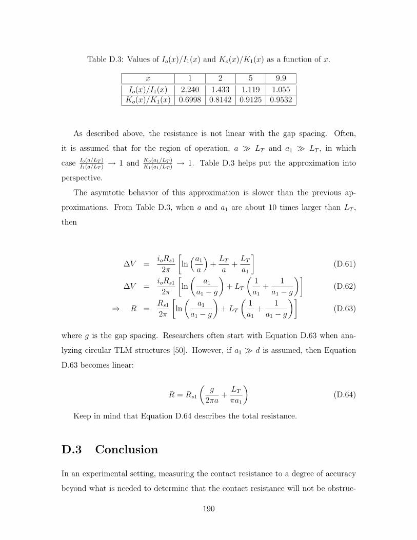
D.3 Values of Io(x)/I1(x) and Ko(x)/K1(x) as a function of x. . . . . . . 190
20
Chapter 1
Introduction
Today’s technological advancements in electronics often go hand-in-hand with ad-
vancements in optics. For example, as recent developments in low-power electronics
for mobile devices are announced, new designs for liquid crystal display (LCD) and
light emitting diode (LED) technologies for the screens of those same devices are
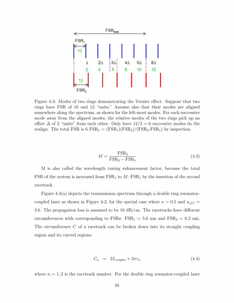
implemented. As lighter-weight, higher-capacity batteries are created and deployed,
higher-efficiency photovoltaic modules are being invented and manufactured. As com-
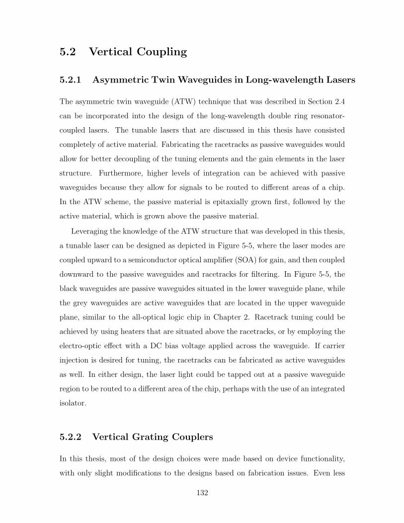
puters acquire better graphics processors for video and gaming, fiber-optic telecom-
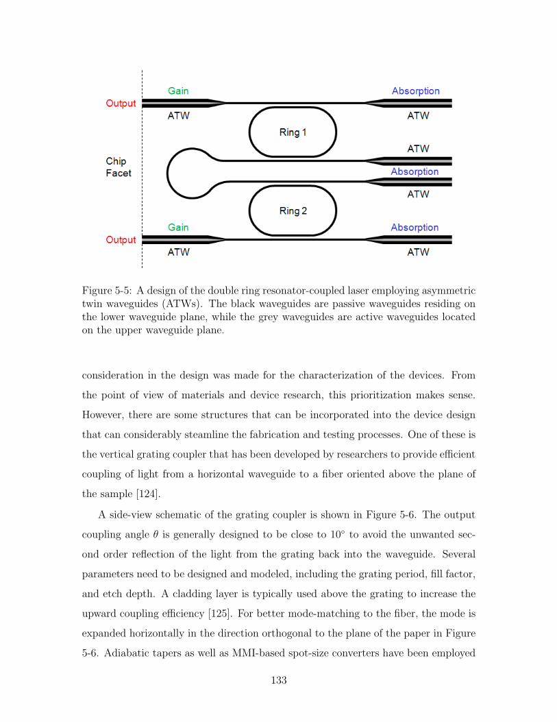
munications research keeps global network bit-rates ahead of the growing bandwidth
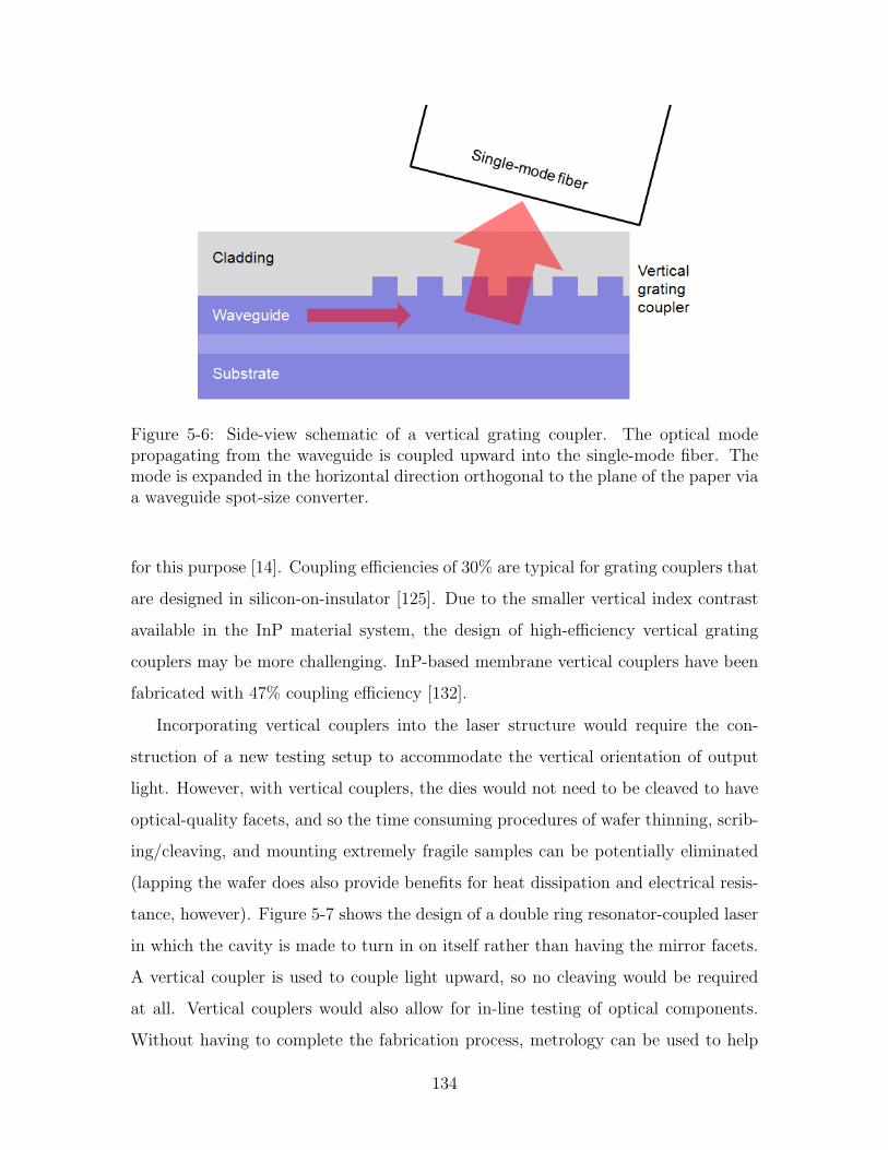
requirements.
Silicon’s versatility and low cost has made it the material of choice for many
electronic and optical devices. However, there are other semiconductors that have
advantages over silicon in certain respects. For example, III-V semiconductors, such
as gallium arsenide (GaAs) and indium phosphide (InP), have a much higher electron
mobility than silicon, and have been used to make high-power and high-frequency
electronics. Furthermore, unlike silicon, III-V semiconductors have a direct bandgap,
allowing them to efficiently emit and absorb photons with energies slightly above their
respective bandgaps. In fact, there are no commercial optical emitters today that
are silicon-based. While a lot of photovoltaics today are silicon-based, the highest-
efficiency solar panels are still the ones fabricated out of III-V semiconductors.
III-V semiconductors also have the added potential of monolithic integration that
21
many other optical materials do not possess. The rapid pace of advancement for
electronic circuits has been largely due to scaling, which could not have been possible
without integration. Integration refers to the placement of all of the components of a
system on the same chip. Monolithic integration describes the fabrication of the entire
chip out of a single wafer. In contrast, hybrid integration describes the fabrication of
certain components of a chip out of different wafers and then assembling the pieces
together in the form of a single chip. Not only does monolithic integration allow
complex systems to have a smaller footprint (and therefore lower costs), it also greatly
simplifies the assembly process that would be required if all of the components were
discrete, or if hybrid integration is employed. The fact that III-V semiconductors
are well-suited to monolithic integration make III-V photonics an exciting area of
research.
Integration is necessary, but not sufficient, for scaling to take place. Integrated
photonics, or photonic integrated circuits (PICs), have remained approximately the
same size over the past ten years. The dimensions for optical devices have not been
limited by lithography, but rather by geometries suitable for low-loss light prop-
agation. One of the hurdles that integrated photonics still faces is the lack of a
universally-accepted building block that is comparable in functionality and versatil-
ity to the transistor for ICs. The integrated photonic equivalent of an electronic wire,
however, is widely accepted to be the ridge waveguide.
This thesis explores devices constructed in the indium phosphide material system,
which is an important subset of III-V semiconductors. The InP material system
includes ternary and quaternary III-V semiconductors that are lattice-matched to InP,
such as InGaAs, InGaAsP, InGaAlAs, and InAlAsP. Devices operating at different
wavelengths, from the primary fiber-optic telecommunications wavelength of 1.55 µm
up to 2 µm are investigated. Along the way, three different waveguide-based building
blocks for integrated photonics will be examined: (1) the Fabry-Perot resonator, (2)
the Mach-Zehnder interferometer, and (3) the microring resonator.
22
1.1 The Indium Phosphide Material System
Indium phosphide is a binary III-V semiconductor that has a crystal structure of
two overlapping face-centered cubic lattices with a lattice constant of 5.87 A [103].
While not as cheap as Si, InP is available as large wafers at moderate prices, making
it attractive for the study and, in some cases, production of electrical and photonic
devices. Because its electron mobility is much higher than that of silicon, InP can
be found in communications devices where high speed is a necessity. Indium phos-
phide has a direct bandgap of 1.344 eV at room temperature, which corresponds to
the near-infrared wavelength of 923 nm. One of the advantages of InP is that it
can be used as a substrate for the epitaxial growth of other III-V semiconductors.
By combining one or more binary compounds (e.g GaAs, InP, InAs), it is possible
to create ternary (e.g. InGaAs, InAlAs) and quaternary (e.g InGaAsP, InGaAlAs)
compounds [103]. For the purposes of this thesis, all of these materials will be con-
sidered as part of the InP material system. In three-dimensional bulk form, these
materials are limited to emission wavelengths corresponding to their bandgap ener-
gies. In reduced-dimensionality forms, such as quantum wells and quantum dots,
the emission/absorption wavelengths can be even more precisely tailored. If strained
materials are also introduced, the InP material system has the ability to cover the
wavelength range of 0.9 µm to 2 µm [135]. Fortunately, the bandgap energy has an
inverse relationship with refractice index, which allows the use of the larger-bandgap
materials, such as InP itself, as the cladding of a waveguide, and the smaller-bandgap
material, such as InGaAs, as the core of a waveguide [22].
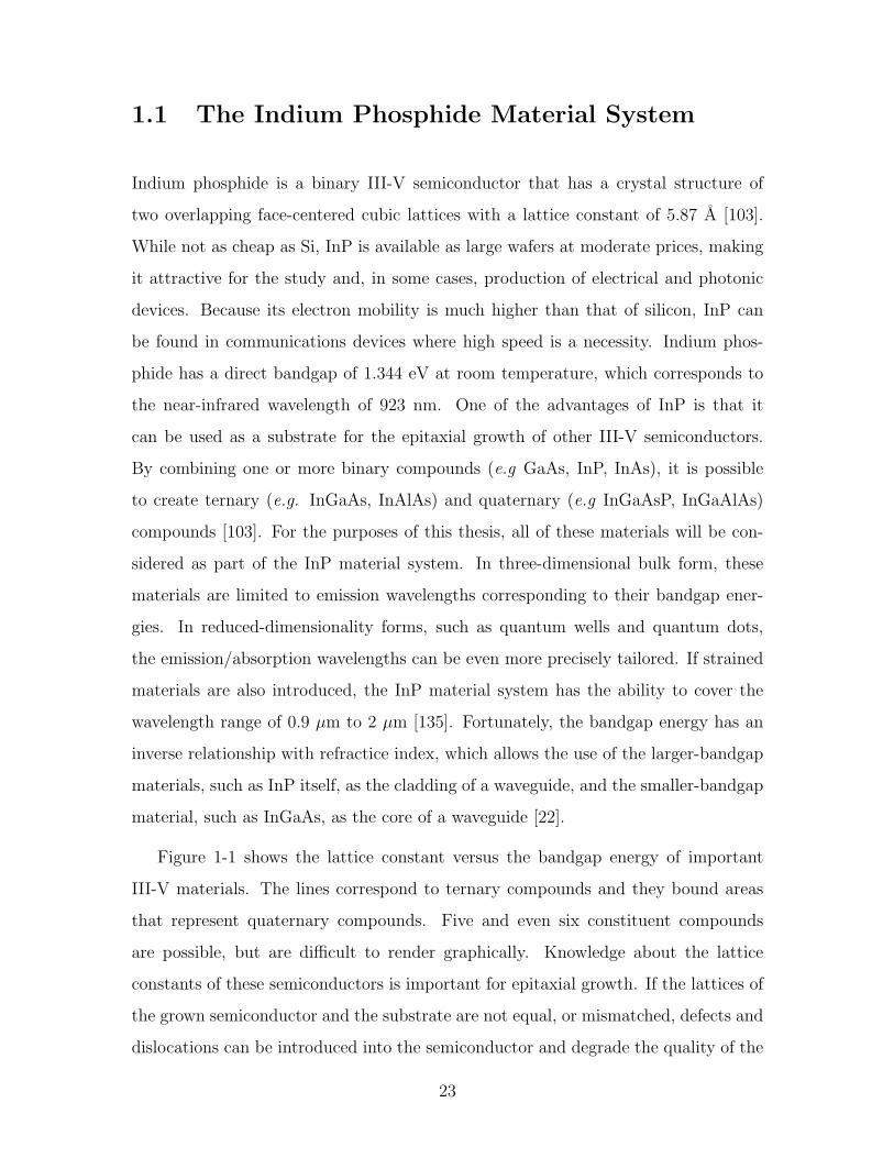
Figure 1-1 shows the lattice constant versus the bandgap energy of important
III-V materials. The lines correspond to ternary compounds and they bound areas
that represent quaternary compounds. Five and even six constituent compounds
are possible, but are difficult to render graphically. Knowledge about the lattice
constants of these semiconductors is important for epitaxial growth. If the lattices of
the grown semiconductor and the substrate are not equal, or mismatched, defects and
dislocations can be introduced into the semiconductor and degrade the quality of the
23
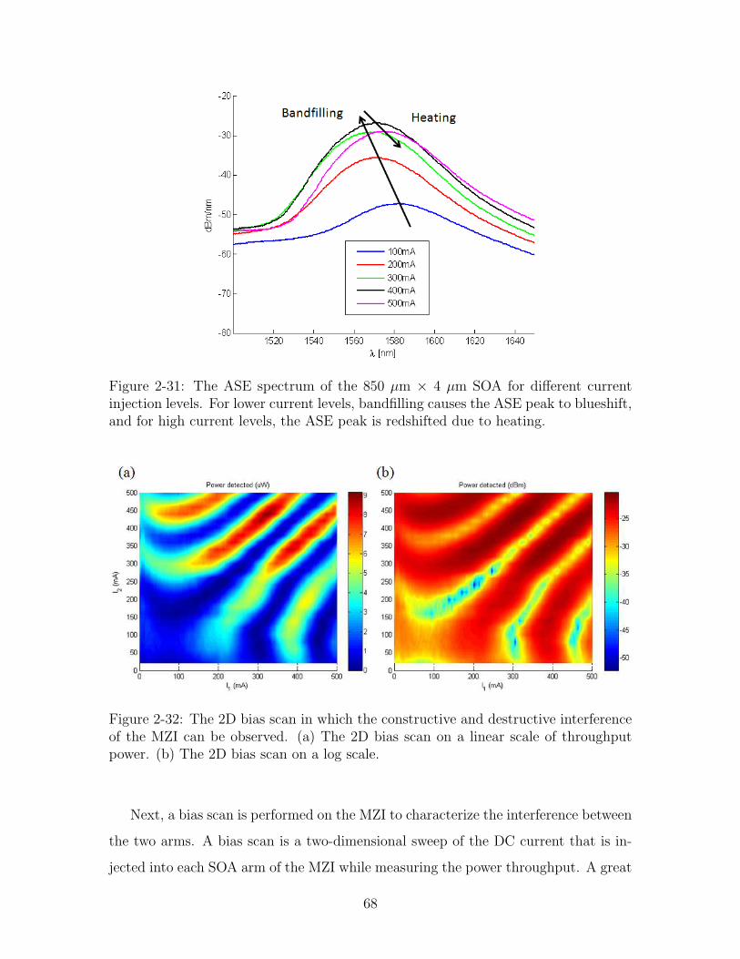
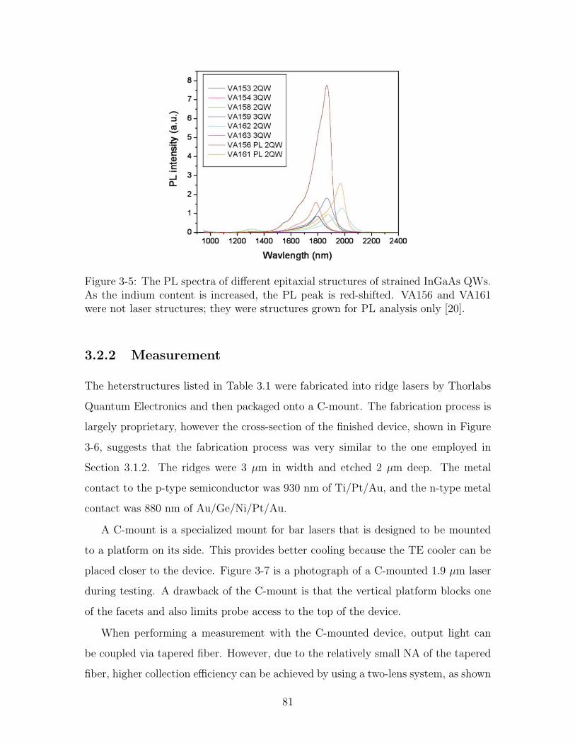
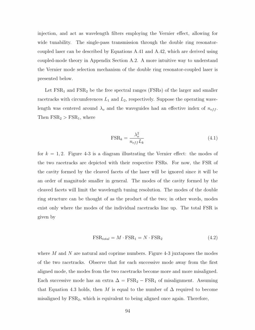
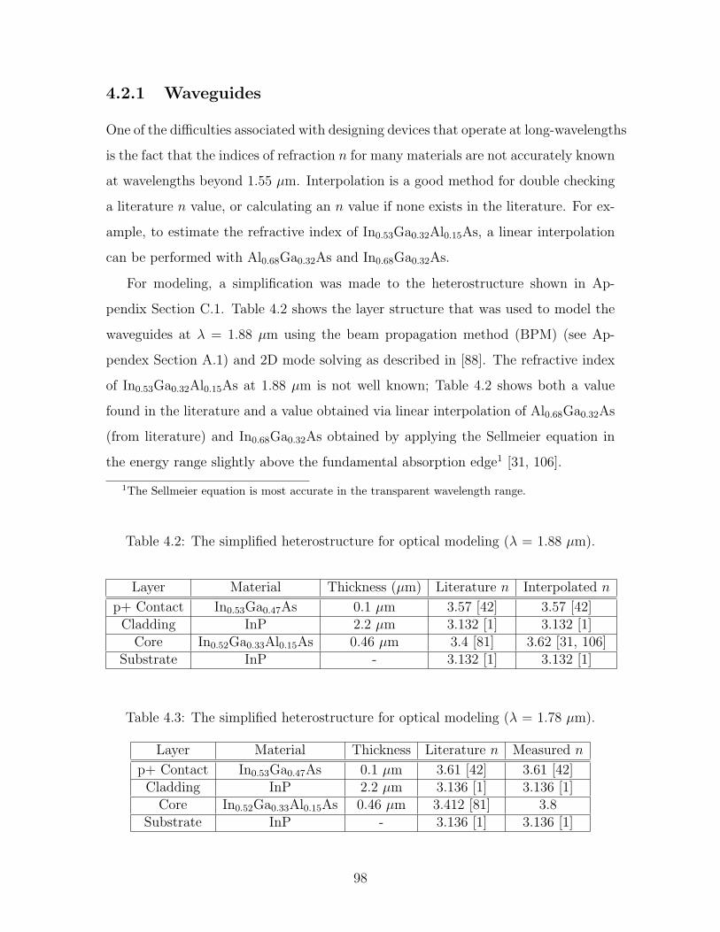
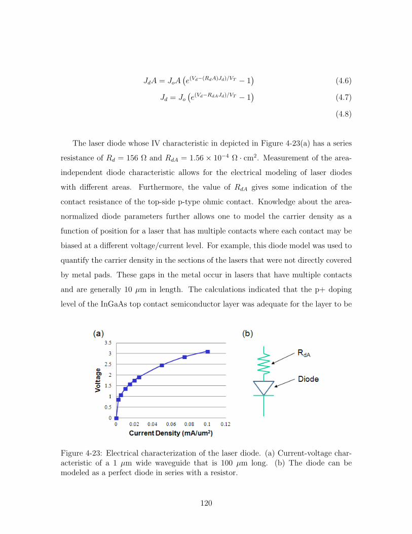
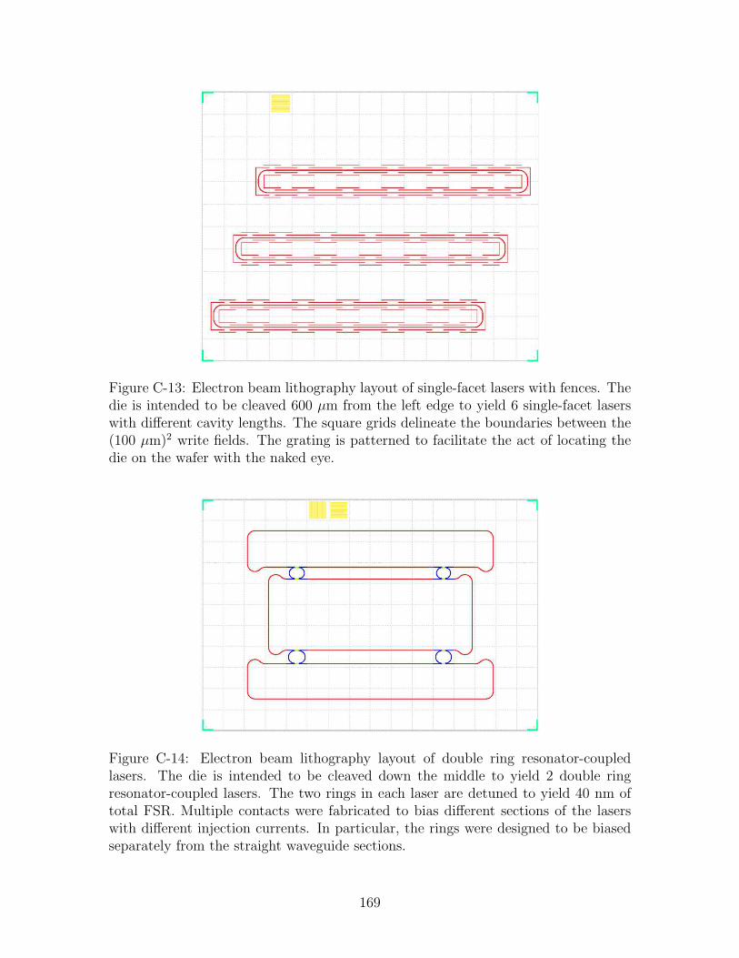
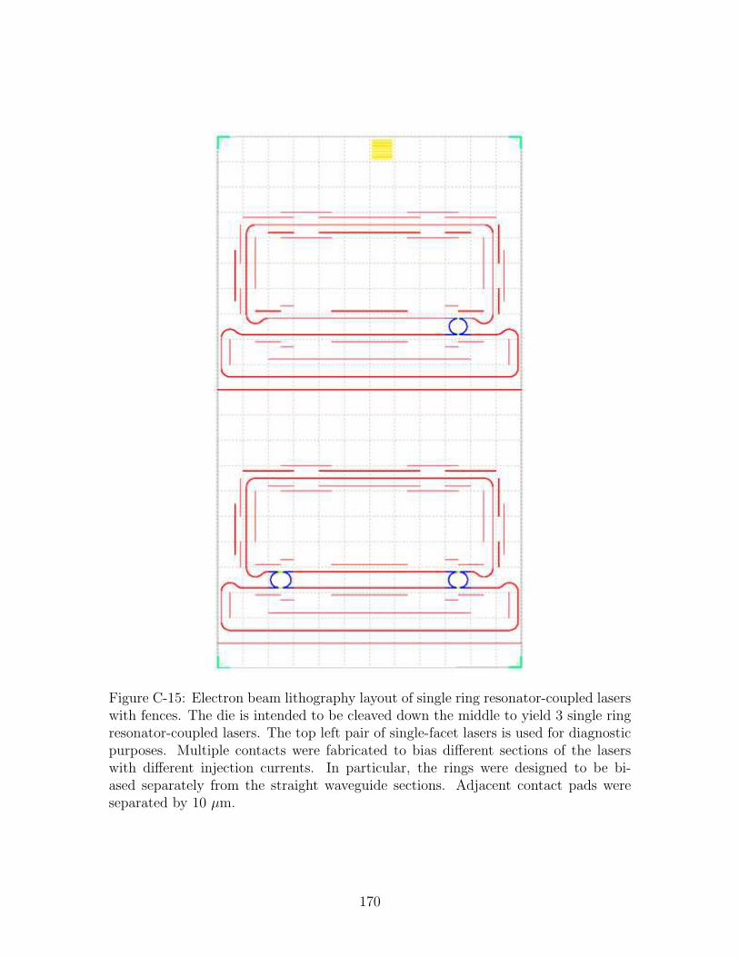
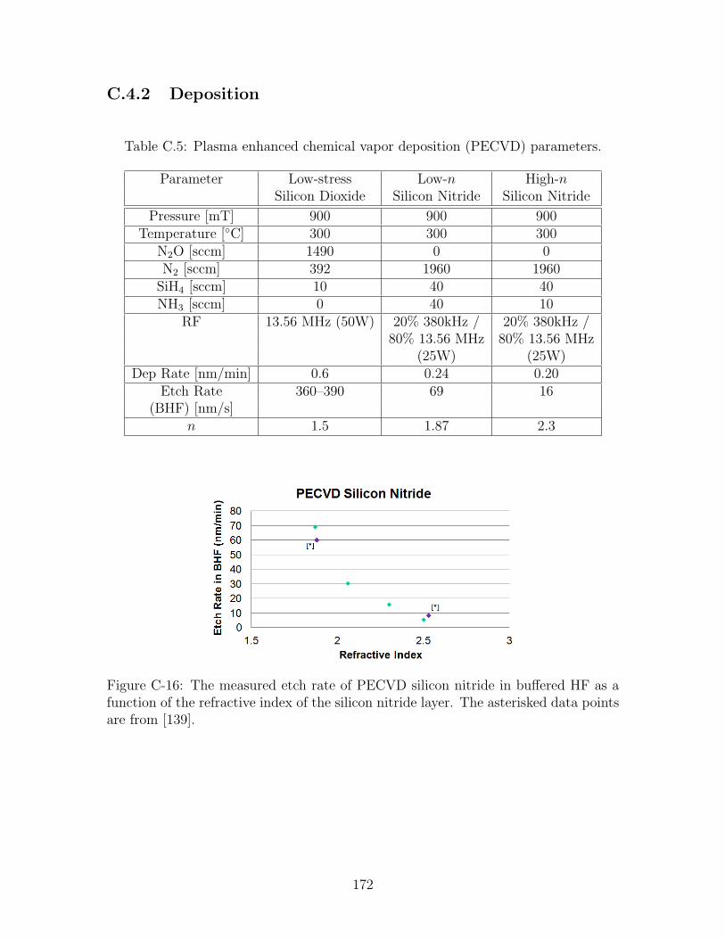
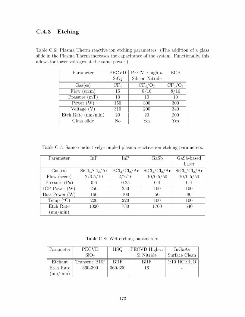
Figure 1-1: The bandgap energy versus the lattice constant of III-V semiconductors[103]. The lines connecting the binary semiconductors represent ternary semiconduc-tors.
film. The vertical lines represent the epitaxial constraints of growing on a particular
substrate. In certain situations, however, lattice mismatches are desired, such as for
the growth of strained materials or quantum dot materials as will be discussed in
Chapter 3.
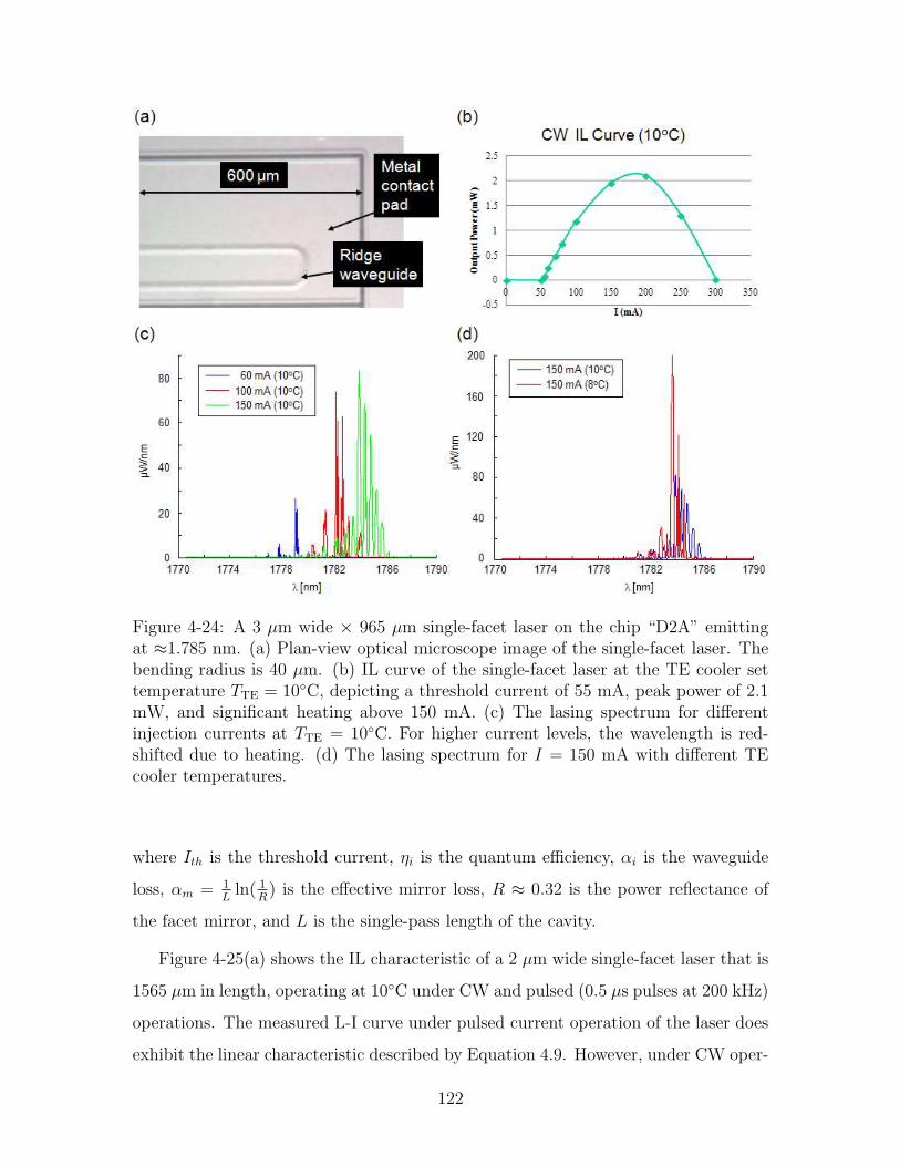
1.2 Integrated Photonic Waveguide Building Blocks
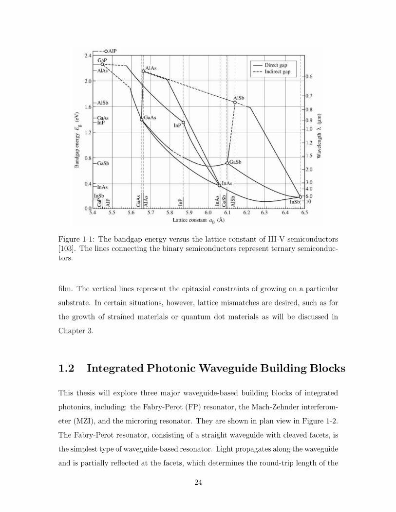
This thesis will explore three major waveguide-based building blocks of integrated
photonics, including: the Fabry-Perot (FP) resonator, the Mach-Zehnder interferom-
eter (MZI), and the microring resonator. They are shown in plan view in Figure 1-2.
The Fabry-Perot resonator, consisting of a straight waveguide with cleaved facets, is
the simplest type of waveguide-based resonator. Light propagates along the waveguide
and is partially reflected at the facets, which determines the round-trip length of the
24
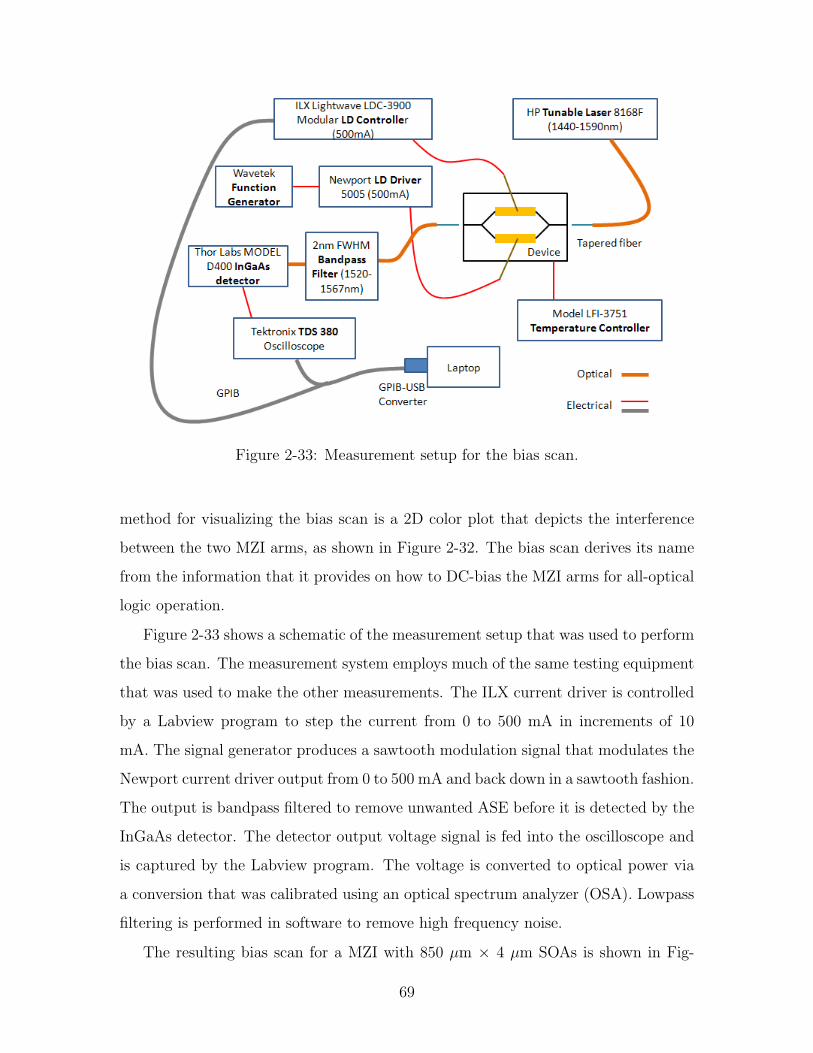
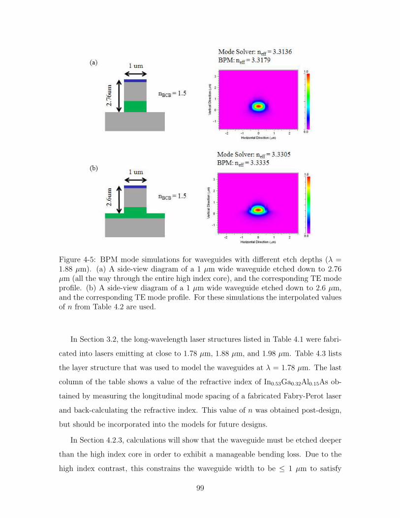
Figure 1-2: (a) A Fabry-Perot cavity: light propagates along the waveguide and ispartially reflected and partially transmitted at the mirror facets. Only wavelengthsthat interfere constructively in the cavity will receive positive feedback if there isgain. (b) A Mach-Zehnder interferometer (MZI): light that propagates within theMZI experiences a 50-50 power split. After traveling through the respective arms ofthe Mach-Zehnder, the light is recombined (interfered) as the two arms meet at theoutput waveguide. The output is zero when destructive interference occurs. (c) Amicroring resonator: input light is evanescently coupled to the ring only if an integernumber of wavelengths fit in a round trip of the ring resonator. The light in the ringcan be coupled back out to another waveguide.
cavity, or etalon. If gain is introduced, the wavelengths that interfere constructively
in the cavity will experience positive feedback [22].
Mach-Zehnder interferometers are very versatile interferometric structures that are
well-suited to integration. In many free-space optical interferometric structures, the
light paths overlap. However, in integrated waveguide structures, crossing lightpaths
without crosstalk is difficult, and the integrated MZI is able to eliminate them. In an
MZI, the light first experiences a 50-50 power split. Then, after traveling through the
respective arms of the Mach-Zehnder, the light is interfered at the output waveguide
[100].
A microring resonator is a wavelength selective device, much like a Fabry-Perot
resonator, but the feedback mechanism is inherent in the geometry of the rings. The
rings can be made to have round-trip lengths that are generally smaller than that of
ridge FP resonators due to cleaving constraints, making the free-spectral range (FSR)
of the rings larger than that of FP resonators [90].
25
1.3 Thesis Organization
In Chapter 2, integrated all-optical logic (AOL) gates operating at the wavelength
of 1550 nm will be investigated. All-optical logic has the potential to transform
telecommunications and beyond. In this chapter, I present the design of an integrated
AOL unit cell based on an MZI structure with electrically-pumped semiconductor
optical amplifiers (SOAs) as nonlinear elements. The operation of dilute waveguides
and asymmetric twin waveguides for coupling between the passive waveguides and
SOAs is demonstrated. The carrier-dependent interference of the MZI is visualized
by performing a static bias scan, which allows the DC operating point for the AOL
unit cell to be successfully determined.
Chapter 3 delves into Fabry-Perot ridge diode lasers with gain from active material
layers in which lattice mismatches are intentionally introduced. InAs quantum dots
with gain near the wavelength of 1.55 µm and strained InGaAs quantum wells with
gain in the wavelength range of 1.55 µm to 2 µm are characterized.
Chapter 4 examines tunable ring resonator-coupled lasers emitting at 1.78 µm,
1.88µm, and 1.98 µm. Tunable long-wavelength lasers have applications in tunable
diode laser absorption spectroscopy (TDLAS) for trace-gas sensing. An assortment
of gases have absorption lines in the 1.55 µm to 2 µm wavelength range. The ring
resonator-coupled lasers are designed so that wavelength tuning can be achieved with
carrier injection into the rings. Double ring resonator-coupled lasers are designed
with a slight detuning in the FSR of the two rings, which gives rise to wide tunability
due to the Vernier effect.
In Chapter 5, conclusions and future work are presented.
26
Chapter 2
Integrated All-Optical Logic and
Wavelength Conversion
The fast-paced improvement in technology over the past three decades has been
largely due to the advancement of digital logic in the form of electronic integrated
circuits (ICs). As the workhorse of the digital IC industry, complementary metal-
oxide-semiconductor (CMOS) technology has been extremely amenable to scaling:
the density of transistors in microprocessors has doubled approximately every 18
months [102]. While electronics are well-suited to performing dense information pro-
cessing, information transmission may be better accomplished in the optical domain
[3]. With the advent of fiber-optic communications and, more recently, integrated
photonics, copper has been gradually replaced by optical components. Recent devel-
opments in fiber-to-the-home and on-chip optical interconnects depict the on-going
switch from electronic to optical signal transmission [32, 72]. Many believe that it is
possible for integrated circuits to be replaced by so-called photonic integrated circuits
(PICs) that perform digital logic with photons rather than electrons. As Moore’s Law
slows down, PICs are beginning to emerge as a promising technology with advantages
over electronic ICs in speed and power consumption [22].
One of the success stories of modern-day technological innovation is the Internet.
From its advent in the 1980s to the present, the Internet has revolutionized both com-
munications and the media. Since 1990, a vast network of intercity and transoceanic
27
fiber-optic cables has been installed to increase Internet capacity. Today, the state-of-
the-art long-distance broadband Internet is relayed through these fiber cables at bit
rates of up to 40 Gb/s per channel, transmitting thousands of petabytes a day. Using
wavelength division multiplexing (WDM), over 100 different channels are transmitted
through a single fiber [41]. This seemingly large capacity is being consumed rapidly
however, as international Internet traffic rises at an average rate of 75% a year [127].
Between 2004 and 2006 alone, U.S. broadband access increased by almost 65% [107].
Unfortunately, during the same time frame, Internet capacity has only increased by
an annual rate of 45%. Furthermore, the increase in Voice over Internet Protocol
(VoIP) applications, video and music streaming websites, and peer-to-peer file trans-
fer programs put a significant additional strain on Internet bandwidth. Without an
acceleration in the expansion of Internet capacity, Internet congestion can become a
problem with large-scale economic consequences.
The solutions to the Internet capacity problem can be categorized as either parallel
or series approaches. For example, a parallel approach would be to lay more fiber-
optic cables into the ground, creating more parallel channels for transmission. A
series approach would be to increase the capacity of the existing fiber infrastructure
by swapping out bandwidth-limiting components for faster technologies. As it turns
out, the series approach is more attractive than the parallel approach, since laying
down more fiber-optic cables is a very expensive effort. In this chapter, ways to
increase the bit rates transmitted through the existing fiber cables are investigated.
Routers play an important role in optical fiber telecommunication networks to-
day, directing transmitted data to their correct destinations. Wavelength conversion
is an important component of routing in current circuit-switched WDM networks. In
packet-switched networks, header processing is necessary for routing. Regenerators
are used along with routers to perform reamplification, reshaping, and retiming (3R-
regeneration) on optical data. 3R-regeneration is also used to eliminate the added
noise from amplifiers in long-distance transmissions. Routing and regeneration of op-
tical signals require electronic logic operations, and therefore conversions between the
optical and electronic domains. These optical-to-electronic-to-optical (O/E/O) con-
28
versions take place at each regenerator and router node, putting limits on the speed,
cost, and power consumption of the regenerating and routing operations. To increase
bit rates and transmission channels, the O/E/O bottleneck must be addressed.
One of the ways to address the cost of O/E/O conversions is integration. The
company Infinera has developed ten-channel 10 Gb/s and 40 Gb/s transmitter and
receiver chips for O/E/O conversion that are monolithically integrated in indium
phosphide [77]. By integrating lasers, modulators, detectors, multiplexers, and atten-
uators onto a single PIC, they have reduced the costs of manufacturing and packaging,
thus making O/E/O conversions less of a bottleneck than before.
We propose to eliminate O/E/O conversions altogether. That is, to perform
routing, 3R-regeneration, and wavelength conversion directly in the optical domain.
In fact, electronic processing, when compared to all-optical processing, underperforms
in the areas of latency (and therefore buffering requirements) and power consumption
[65]. Furthermore, if the all-optical processor is monolithically integrated, the cost
can be driven down to a price-point that is competitive for large-scale deployment.
To perform digital processing on a PIC, the first step is to create photonic equiv-
alents of electronic processing building blocks. The two fundamental building blocks
of digital ICs are the logic gate and the flip-flop, or more broadly, the processing
unit and the memory unit. In this chapter, all-optical logic is investigated, although
all-optical memory, or buffering, is a very interesting area of research as well.
The most rudimentary all-optical buffers consist of delay lines or recirculating
loops [137]. A recirculating loop is a loop in which the optical data is made to
circulate until it is coupled out when needed. Often, a regenerator is placed in the
loop to compensate for fiber losses and distortions. Delay lines and recirculating
loops can be designed to provide variable delays [137]. Variable delays have also
been achieved using fiber dispersion by taking advantage of the different group delays
that different wavelengths experience [19]. Data can be converted to the wavelength
corresponding to the desired delay, transmitted through the delay line, and converted
back to its original wavelength at the output [138]. Another promising method for
providing all-optical buffers is “slow light,” although most demonstrations show only
29
about a pulse-width of delay [80, 144]. “Slow light” is achieved by exploiting peaks in
the dispersion relation of either the material or the waveguide that a signal propagates
in. The group velocity of a pulse can be made to be hundreds of times slower than
the speed of light.
2.1 All-Optical Logic
All-optical logic (AOL) provides a framework for eliminating the expensive O/E/O
conversions in fiber-optic networks. Routing and regeneration performed completely
in the optical domain can reduce power consumption, latency, and complexity. An
AOL gate is a device with optical input and output ports, where the outputs are
causally dependent on the inputs. Because the optical signals must interact with each
other, an AOL gate is inherently optically nonlinear. Demonstrations of all-optical
logic have been achieved by exploiting the nonlinearities in passive materials such as
silica (SiO2) fiber, passive semiconductors, and even organic molecules [28, 143, 146].
Actively pumped semiconductors, such as semiconductor optical amplifiers (SOAs),
have been successfully demonstrated to exhibit even larger nonlinearities [115].
The nonlinear interaction of optical signals can cause changes in phase, and to
a lesser degree, power. Because of this, all-optical switching techniques most often
utilize some sort of interference to take advantage of the phase change. All-optical
switches have been demonstrated utilizing cross-phase modulation in resonating struc-
tures [143]. All-optical demultiplexing of 160 Gb/s data streams has been demon-
strated using nonlinear optical loop mirrors [123]. Up to 100 Gb/s logic operation
has been demonstrated with the ultrafast nonlinear interferometer (UNI), as well as
40 Gb/s packet routing [36, 136]. The UNI was the first high-speed all-optical logic
gate to be demonstrated in a single-arm interferometer [85, 86]. All-optical logic has
also been demonstrated with Mach-Zehnder interferometers (MZIs) that have semi-
conductor optical amplifiers (SOAs) in each arm [25]. These MZI structures have also
shown wavelength conversion at bit rates of 168 Gb/s, along with demultiplexing at
336 Gb/s [129, 78].
30
The SOA is a very interesting device because it is not only capable of achieving
large nonlinearities, but is also well-suited for integration. For all-optical logic to
become a viable part of telecommunication networks, it needs to be integrated. The
majority of the all-optical logic demonstrations (including those described above)
have been performed with configurations set up on an optical bench. Discrete SOAs
and fibers, however, present size, cost, and packaging issues that can be solved by
monolithic integration. The challenges of designing and building an integrated device
are quite different from that of making the device out of fiber and discrete components.
2.2 Semiconductor Optical Amplifiers
Semiconductor optical amplifiers (SOAs), also often called semiconductor laser am-
plifiers, were first developed as amplifiers in optical transmission networks. However,
the SOA possessed poor noise performance, recovery-time-induced patterning effects,
and lower saturated output power than its fiber-based counterpart, the erbium-doped
fiber amplifier (EDFA), which became the amplifier of choice in optical networks. The
SOA does have some advantages over the EDFA, however, such as being electrically
pumped, rather than optically pumped. Furthermore, SOAs are well-suited for inte-
gration because semiconductor materials can be epitaxially grown on semiconductor
wafers. These qualities make the SOA a very useful building block in PIC applica-
tions.
A SOA is structurally a laser diode without mirrors. Like a laser diode, carrier
injection inverts the carrier population and creates gain. With no mirrors, any photon
traveling in the SOA will make a single pass through the device. Because of this,
the electroluminescence of the SOA, called amplified spontaneous emission (ASE), is
representative of the gain spectrum of the device [22]. SOAs provide gain and exhibit
large nonlinearities for wavelengths with photon energies that are slightly above the
bandgap of the gain material that is used [115].
The nonlinearity in a SOA arises due to stimulated emission, which depletes the
free carriers and decreases the gain. This creates a change in the refractive index of
31
the SOA, as governed by the Kramers-Kronig relation. Only a small number of free
carriers are needed to be depleted in order to create a nonlinear index change that
is useful in integrated waveguide structures. The active injection of carriers, allows
for relatively fast recovery times, on the nanosecond time scale down to hundreds of
picoseconds, for high injection levels [64].
Quantum dot (QD) SOAs have been measured to have recovery times as short
as 15 ps [148]. Quantum dots confine electrons in three dimensions, creating a 3D
potential well that “squeezes” the electronic energy levels into atomic-like quantized
steps. The energy level spacings depend on the size of the QD; the smaller the QD,
the fewer the bound states the QD will possess. One of the benefits of having only
a handful of energy levels is that fewer carriers are required to achieve population
inversion. Typically, a QD found in an SOA will have two bound states, a “ground”
state and an “excited” state [130]. The QD layers are grown with very high lattice
mismatch, the stress of which causes the layer to self-assemble into small islands, the
quantum “dots,” rather than form a continuous layer. Beneath the QD layer is the
wetting layer, which can be considered a reservoir of carriers for the QDs because of
its large number of carriers compared to the bound electrons and holes of the QDs.
Thus, when stimulated emission depletes the carriers of the QDs, this reservoir of
carriers quickly replenishes the supply, leading to very fast recovery times [74].
2.3 Integrated All-Optical Logic Gate and Wave-
length Converter Design
Utilizing the large nonlinearities of SOAs and their compatibility with integration,
along with the performance of MZI structures for AOL, the integrated all-optical logic
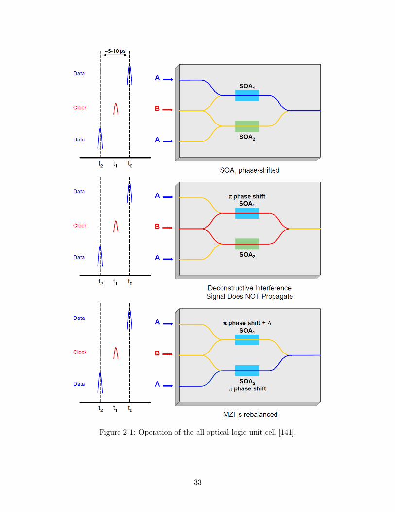
gate that is depicted in Figure 2-1, was designed [65, 137, 141]. The device, called the
all-optical logic unit cell, consists of a MZI with SOAs in both arms. The MZI has
three input ports. A signal sent into the top or bottom port will travel through the
top or bottom arm of the MZI, respectively. A signal sent into the middle port will
32
Figure 2-1: Operation of the all-optical logic unit cell [141].
33
encounter a 50-50 power split and travel through both arms of the MZI. The input
signals do not have to be at the same wavelength; at the output a wavelength filter
can be placed to select for the desired output wavelength. The AOL unit cell can be
cascaded to perform any logic operation and is inherently a wavelength conversion
device. While the general design is wavelength-independent, the target wavelength
of operation for the AOL chip was 1550 nm, the primary wavelength that is used in
fiber-optic telecommunications.
To understand the operation of the AOL unit cell, consider the example that is
illustrated in Figure 2-1. At time t = t0, the signal “A” at a wavelength λA, which
consists of a data pulse (representing a logical 1), is transmitted into the top input
port. As the pulse travels through the top arm of the MZI, the pulse nonlinearly
changes the refractive index of SOA1, causing the optical phase delay in SOA1 to
be π-phase shifted with respect to that in SOA2. The DC bias of the SOAs and
the intensity of the pulse must be calibrated to achieve the desired π phase shift.
For the time being, assume that the calibration has been achieved. Less than 10 ps
later, at time t = t1, signal “B”, which also consists of a data pulse (representing
a logical 1), arrives in the middle input port. In this example, signal “B” is at a
different wavelength, λB. At the output, there is a filter selecting for λB. Because the
two SOAs are out of phase, destructive interference occurs at the output for signal
“B.” The output is a logical 0. If signal “A” had been a logical 0, then the output
would have been a logical 1. If signal “B” is made to be a Clock signal, then the
logical output is equivalent to ¬A or A (boolean operation NOT A). Notice that a
wavelength conversion has taken place as a result of the logic operation, from λA to
λB.
At this point, the AOL unit cell is unbalanced. One can wait for the carriers in
SOA1 to recover, or alternatively, another signal “A” can be transmitted into the
bottom input port to rebalance the MZI arms as shown in the bottom of Figure 2-1.
If rebalancing is not performed, AOL unit cells employing bulk or quantum well SOAs
would only be able to achieve operating rates of low tens of Gb/s. On the other hand,
QD SOAs, with their fast recovery times, can achieve theoretical operating bit rates
34
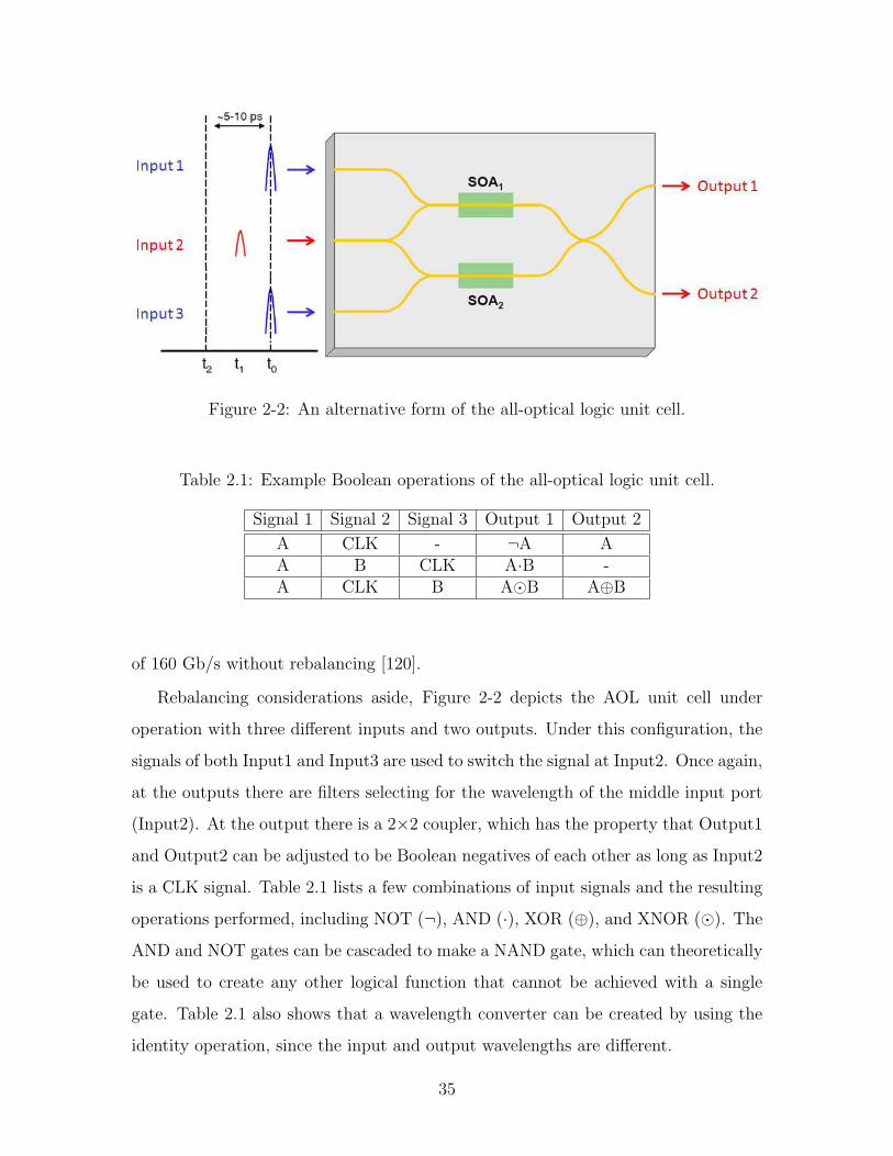
Figure 2-2: An alternative form of the all-optical logic unit cell.
Table 2.1: Example Boolean operations of the all-optical logic unit cell.
Signal 1 Signal 2 Signal 3 Output 1 Output 2
A CLK - ¬A AA B CLK A·B -A CLK B A¯B A⊕B
of 160 Gb/s without rebalancing [120].
Rebalancing considerations aside, Figure 2-2 depicts the AOL unit cell under
operation with three different inputs and two outputs. Under this configuration, the
signals of both Input1 and Input3 are used to switch the signal at Input2. Once again,
at the outputs there are filters selecting for the wavelength of the middle input port
(Input2). At the output there is a 2×2 coupler, which has the property that Output1
and Output2 can be adjusted to be Boolean negatives of each other as long as Input2
is a CLK signal. Table 2.1 lists a few combinations of input signals and the resulting
operations performed, including NOT (¬), AND (·), XOR (⊕), and XNOR (¯). The
AND and NOT gates can be cascaded to make a NAND gate, which can theoretically
be used to create any other logical function that cannot be achieved with a single
gate. Table 2.1 also shows that a wavelength converter can be created by using the
identity operation, since the input and output wavelengths are different.
35
2.4 Active-passive Integration
The AOL unit cell that is depicted in Figure 2-2 can be broken down into active
and passive components. The active components are the SOAs. The passive com-
ponents include the waveguides and the splitters/combiners in the MZI. The active
SOAs need to be fabricated out of semiconductor material that has a bandgap near
the wavelength of operation to provide a large nonlinearity. A potential material is
InxGa1−xAsyP1−y, which can have a bandgap close to the photon energy of 1550 nm
light for x = 0.56 and y = 0.94. During operation, the SOAs need to be electri-
cally pumped above transparency. The passive components need to be fabricated out
of material with a bandgap that is much larger than the photon energy of 0.8 eV
corresponding to 1550 nm light, so that it remains transparent during operation. A
potential material is InP, which has a bandgap energy of 1.34 eV.
The integration of the active and passive components can be achieved in a number
of ways. One method is to epitaxially grow the passive material first, then selectively
etch away regions where the active material is desired and perform another growth
selectively in the etched areas. This method, called regrowth, creates a structure in
which the active and passive sections are butt-coupled and lie on the same plane on
the chip. An alternative is to epitaxially grow the passive material first, and then grow
the active material above. Using a vertical coupling technique, the light can be made
to couple between the lower passive components and the upper active components
[118]. The structure, no longer planar, allows for a relatively straightforward growth
process, but has a challenging fabrication process. The regrowth method has a more
challenging epitaxy process, but a relatively easy fabrication process.
We chose to use a vertical coupling technique known as the asymmetric twin
waveguide (ATW) [70, 118, 142]. The twin waveguide technique was first developed as
index-matched (symmetric) waveguides with directional coupling, however, coupling
efficiencies were low (25%) [16, 119]. The asymmetric twin waveguide technique
utilizes an adiabatic taper to increase the coupling efficiency [73, 116, 117]. With the
adiabatic taper, the top and bottom waveguides do not need to be index-matched.
36
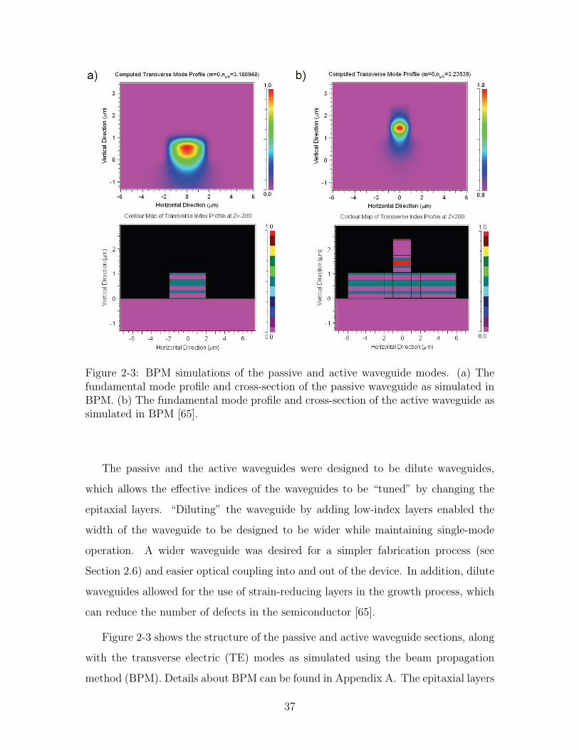
Figure 2-3: BPM simulations of the passive and active waveguide modes. (a) Thefundamental mode profile and cross-section of the passive waveguide as simulated inBPM. (b) The fundamental mode profile and cross-section of the active waveguide assimulated in BPM [65].
The passive and the active waveguides were designed to be dilute waveguides,
which allows the effective indices of the waveguides to be “tuned” by changing the
epitaxial layers. “Diluting” the waveguide by adding low-index layers enabled the
width of the waveguide to be designed to be wider while maintaining single-mode
operation. A wider waveguide was desired for a simpler fabrication process (see
Section 2.6) and easier optical coupling into and out of the device. In addition, dilute
waveguides allowed for the use of strain-reducing layers in the growth process, which
can reduce the number of defects in the semiconductor [65].
Figure 2-3 shows the structure of the passive and active waveguide sections, along
with the transverse electric (TE) modes as simulated using the beam propagation
method (BPM). Details about BPM can be found in Appendix A. The epitaxial layers
37
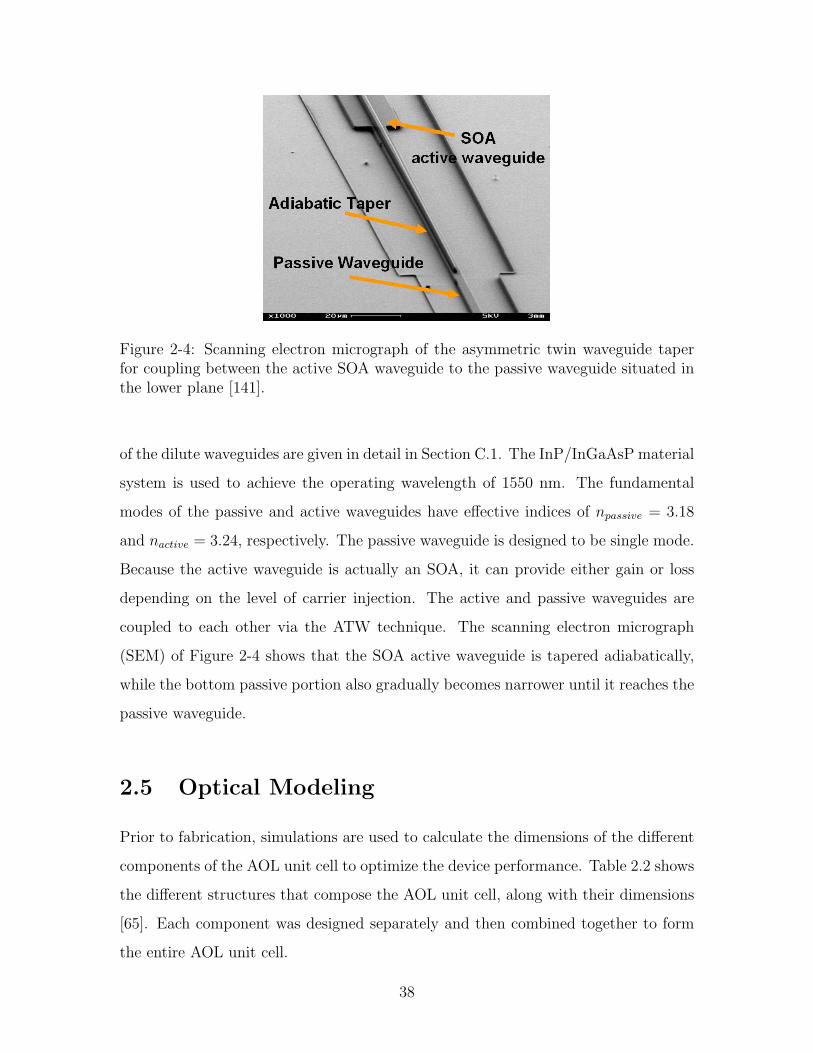
Figure 2-4: Scanning electron micrograph of the asymmetric twin waveguide taperfor coupling between the active SOA waveguide to the passive waveguide situated inthe lower plane [141].
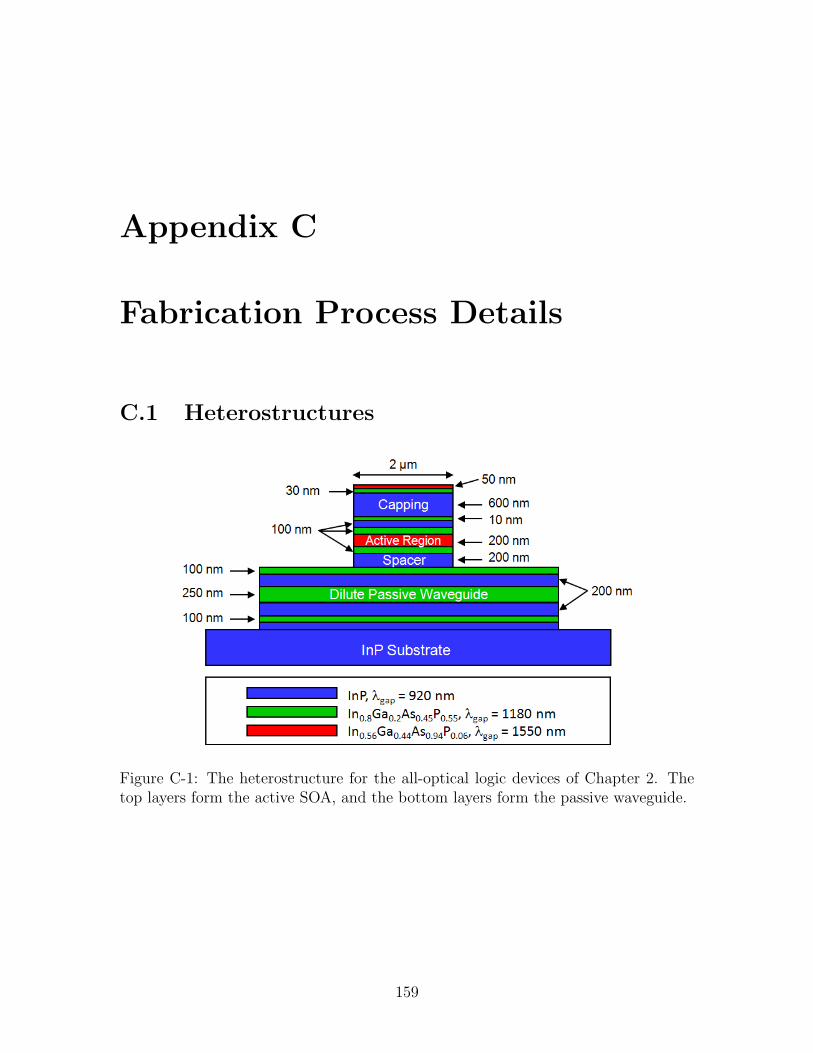
of the dilute waveguides are given in detail in Section C.1. The InP/InGaAsP material
system is used to achieve the operating wavelength of 1550 nm. The fundamental
modes of the passive and active waveguides have effective indices of npassive = 3.18
and nactive = 3.24, respectively. The passive waveguide is designed to be single mode.
Because the active waveguide is actually an SOA, it can provide either gain or loss
depending on the level of carrier injection. The active and passive waveguides are
coupled to each other via the ATW technique. The scanning electron micrograph
(SEM) of Figure 2-4 shows that the SOA active waveguide is tapered adiabatically,
while the bottom passive portion also gradually becomes narrower until it reaches the
passive waveguide.
2.5 Optical Modeling
Prior to fabrication, simulations are used to calculate the dimensions of the different
components of the AOL unit cell to optimize the device performance. Table 2.2 shows
the different structures that compose the AOL unit cell, along with their dimensions
[65]. Each component was designed separately and then combined together to form
the entire AOL unit cell.
38
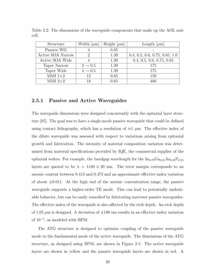
Table 2.2: The dimensions of the waveguide components that make up the AOL unitcell.
Structure Width [µm] Height [µm] Length [µm]
Passive WG 4 0.85 -Active SOA Narrow 2 1.39 0.4, 0.5, 0.6, 0.75, 0.85, 1.0Active SOA Wide 4 1.39 0.4, 0.5, 0.6, 0.75, 0.85
The waveguide dimensions were designed concurrently with the epitaxial layer struc-
ture [65]. The goal was to have a single-mode passive waveguide that could be defined
using contact lithography, which has a resolution of ≈1 µm. The effective index of
the dilute waveguide was assessed with respect to variations arising from epitaxial
growth and fabrication. The intensity of material composition variation was deter-
mined from material specifications provided by IQE, the commercial supplier of the
epitaxial wafers. For example, the bandgap wavelength for the In0.79Ga0.21As0.45P0.55
layers are quoted to be λ = 1180 ± 20 nm. The error margin corresponds to an
arsenic content between 0.413 and 0.473 and an approximate effective index variation
of about ±0.011. At the high end of the arsenic concentration range, the passive
waveguide supports a higher-order TE mode. This can lead to potentially undesir-
able behavior, but can be easily remedied by fabricating narrower passive waveguides.
The effective index of the waveguide is also affected by the etch depth. An etch depth
of 1.05 µm is designed. A deviation of ±100 nm results in an effective index variation
of 10−4, as modeled with BPM.
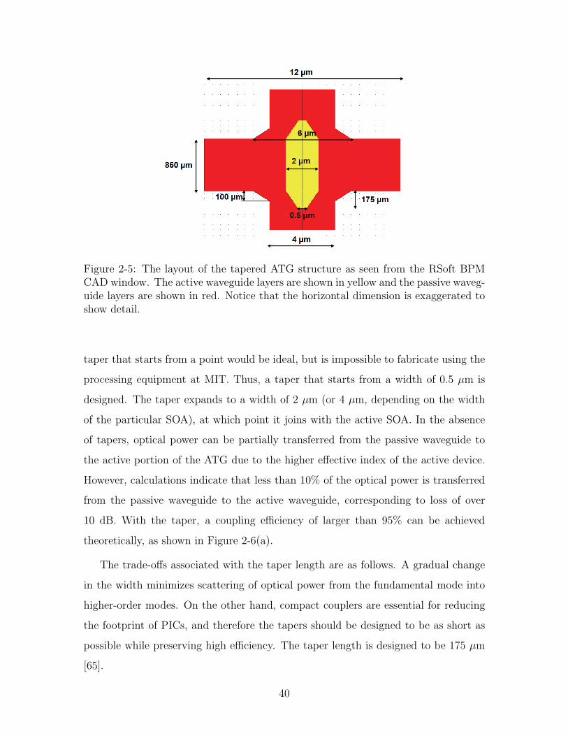
The ATG structure is designed to optimize coupling of the passive waveguide
mode to the fundamental mode of the active waveguide. The dimensions of the ATG
structure, as designed using BPM, are shown in Figure 2-5. The active waveguide
layers are shown in yellow and the passive waveguide layers are shown in red. A
39
Figure 2-5: The layout of the tapered ATG structure as seen from the RSoft BPMCAD window. The active waveguide layers are shown in yellow and the passive waveg-uide layers are shown in red. Notice that the horizontal dimension is exaggerated toshow detail.
taper that starts from a point would be ideal, but is impossible to fabricate using the
processing equipment at MIT. Thus, a taper that starts from a width of 0.5 µm is
designed. The taper expands to a width of 2 µm (or 4 µm, depending on the width
of the particular SOA), at which point it joins with the active SOA. In the absence
of tapers, optical power can be partially transferred from the passive waveguide to
the active portion of the ATG due to the higher effective index of the active device.
However, calculations indicate that less than 10% of the optical power is transferred
from the passive waveguide to the active waveguide, corresponding to loss of over
10 dB. With the taper, a coupling efficiency of larger than 95% can be achieved
theoretically, as shown in Figure 2-6(a).
The trade-offs associated with the taper length are as follows. A gradual change
in the width minimizes scattering of optical power from the fundamental mode into
higher-order modes. On the other hand, compact couplers are essential for reducing
the footprint of PICs, and therefore the tapers should be designed to be as short as
possible while preserving high efficiency. The taper length is designed to be 175 µm
[65].
40
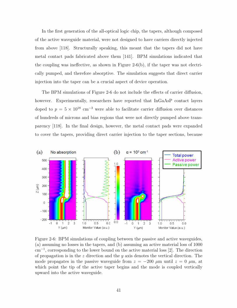
In the first generation of the all-optical logic chip, the tapers, although composed
of the active waveguide material, were not designed to have carriers directly injected
from above [118]. Structurally speaking, this meant that the tapers did not have
metal contact pads fabricated above them [141]. BPM simulations indicated that
the coupling was ineffective, as shown in Figure 2-6(b), if the taper was not electri-
cally pumped, and therefore absorptive. The simulation suggests that direct carrier
injection into the taper can be a crucial aspect of device operation.
The BPM simulations of Figure 2-6 do not include the effects of carrier diffusion,
however. Experimentally, researchers have reported that InGaAsP contact layers
doped to p = 5 × 1018 cm−3 were able to facilitate carrier diffusion over distances
of hundreds of microns and bias regions that were not directly pumped above trans-
parency [118]. In the final design, however, the metal contact pads were expanded
to cover the tapers, providing direct carrier injection to the taper sections, because
Figure 2-6: BPM simulations of coupling between the passive and active waveguides,(a) assuming no losses in the tapers, and (b) assuming an active material loss of 1000cm−1, corresponding to the lower bound on the active material loss [2]. The directionof propagation is in the z direction and the y axis denotes the vertical direction. Themode propagates in the passive waveguide from z = −200 µm until z = 0 µm, atwhich point the tip of the active taper begins and the mode is coupled verticallyupward into the active waveguide.
41
there are other benefits to having larger contacts, such as heat dissipation and ease
of probing.
2.5.2 Multimode Interference Couplers
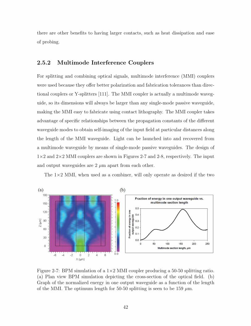
For splitting and combining optical signals, multimode interference (MMI) couplers
were used because they offer better polarization and fabrication tolerances than direc-
tional couplers or Y-splitters [111]. The MMI coupler is actually a multimode waveg-
uide, so its dimensions will always be larger than any single-mode passive waveguide,
making the MMI easy to fabricate using contact lithography. The MMI coupler takes
advantage of specific relationships between the propagation constants of the different
waveguide modes to obtain self-imaging of the input field at particular distances along
the length of the MMI waveguide. Light can be launched into and recovered from
a multimode waveguide by means of single-mode passive waveguides. The design of
1×2 and 2×2 MMI couplers are shown in Figures 2-7 and 2-8, respectively. The input
and output waveguides are 2 µm apart from each other.
The 1×2 MMI, when used as a combiner, will only operate as desired if the two
Figure 2-7: BPM simulation of a 1×2 MMI coupler producing a 50-50 splitting ratio.(a) Plan view BPM simulation depicting the cross-section of the optical field. (b)Graph of the normalized energy in one output waveguide as a function of the lengthof the MMI. The optimum length for 50-50 splitting is seen to be 159 µm.
42
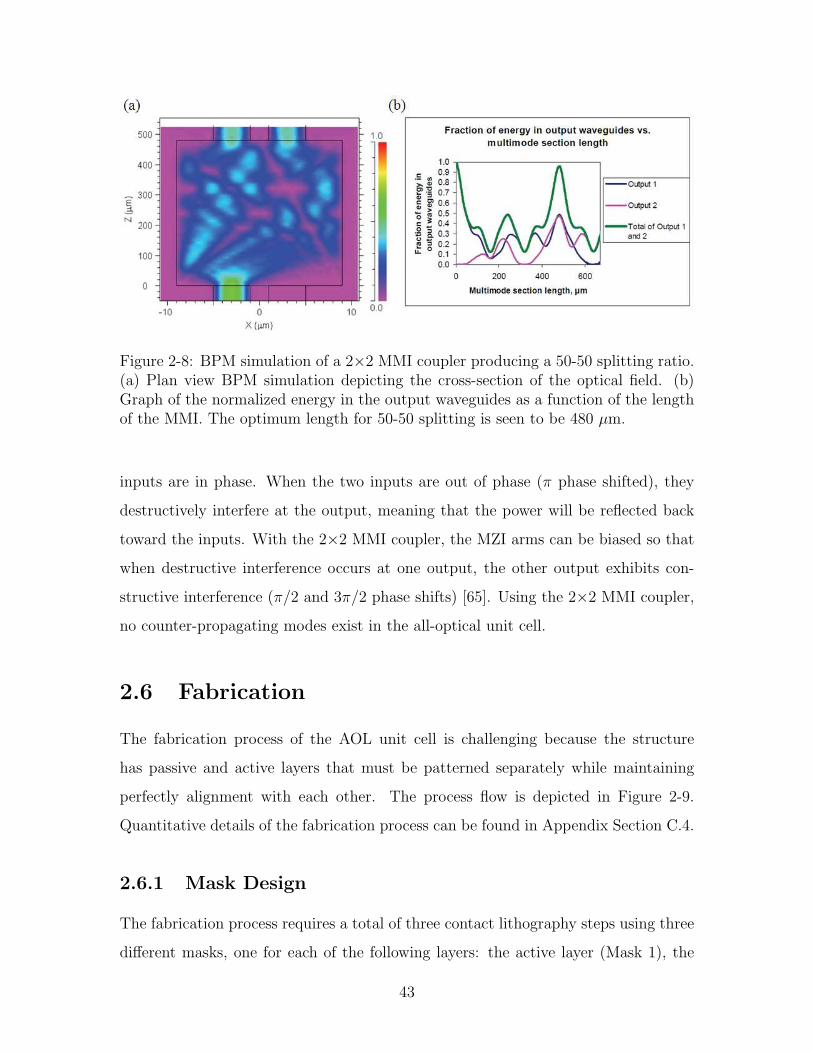
Figure 2-8: BPM simulation of a 2×2 MMI coupler producing a 50-50 splitting ratio.(a) Plan view BPM simulation depicting the cross-section of the optical field. (b)Graph of the normalized energy in the output waveguides as a function of the lengthof the MMI. The optimum length for 50-50 splitting is seen to be 480 µm.
inputs are in phase. When the two inputs are out of phase (π phase shifted), they
destructively interfere at the output, meaning that the power will be reflected back
toward the inputs. With the 2×2 MMI coupler, the MZI arms can be biased so that
when destructive interference occurs at one output, the other output exhibits con-
structive interference (π/2 and 3π/2 phase shifts) [65]. Using the 2×2 MMI coupler,
no counter-propagating modes exist in the all-optical unit cell.
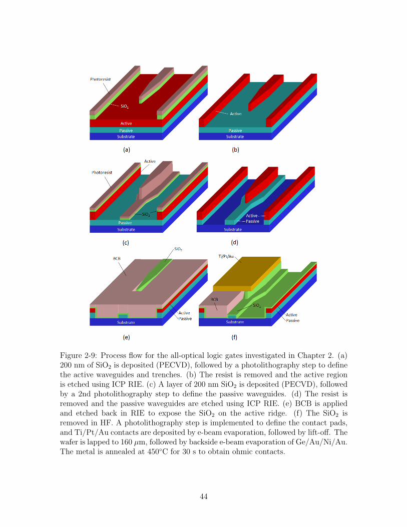
2.6 Fabrication
The fabrication process of the AOL unit cell is challenging because the structure
has passive and active layers that must be patterned separately while maintaining
perfectly alignment with each other. The process flow is depicted in Figure 2-9.
Quantitative details of the fabrication process can be found in Appendix Section C.4.
2.6.1 Mask Design
The fabrication process requires a total of three contact lithography steps using three
different masks, one for each of the following layers: the active layer (Mask 1), the
43
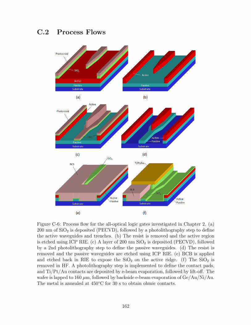
Figure 2-9: Process flow for the all-optical logic gates investigated in Chapter 2. (a)200 nm of SiO2 is deposited (PECVD), followed by a photolithography step to definethe active waveguides and trenches. (b) The resist is removed and the active regionis etched using ICP RIE. (c) A layer of 200 nm SiO2 is deposited (PECVD), followedby a 2nd photolithography step to define the passive waveguides. (d) The resist isremoved and the passive waveguides are etched using ICP RIE. (e) BCB is appliedand etched back in RIE to expose the SiO2 on the active ridge. (f) The SiO2 isremoved in HF. A photolithography step is implemented to define the contact pads,and Ti/Pt/Au contacts are deposited by e-beam evaporation, followed by lift-off. Thewafer is lapped to 160 µm, followed by backside e-beam evaporation of Ge/Au/Ni/Au.The metal is annealed at 450C for 30 s to obtain ohmic contacts.
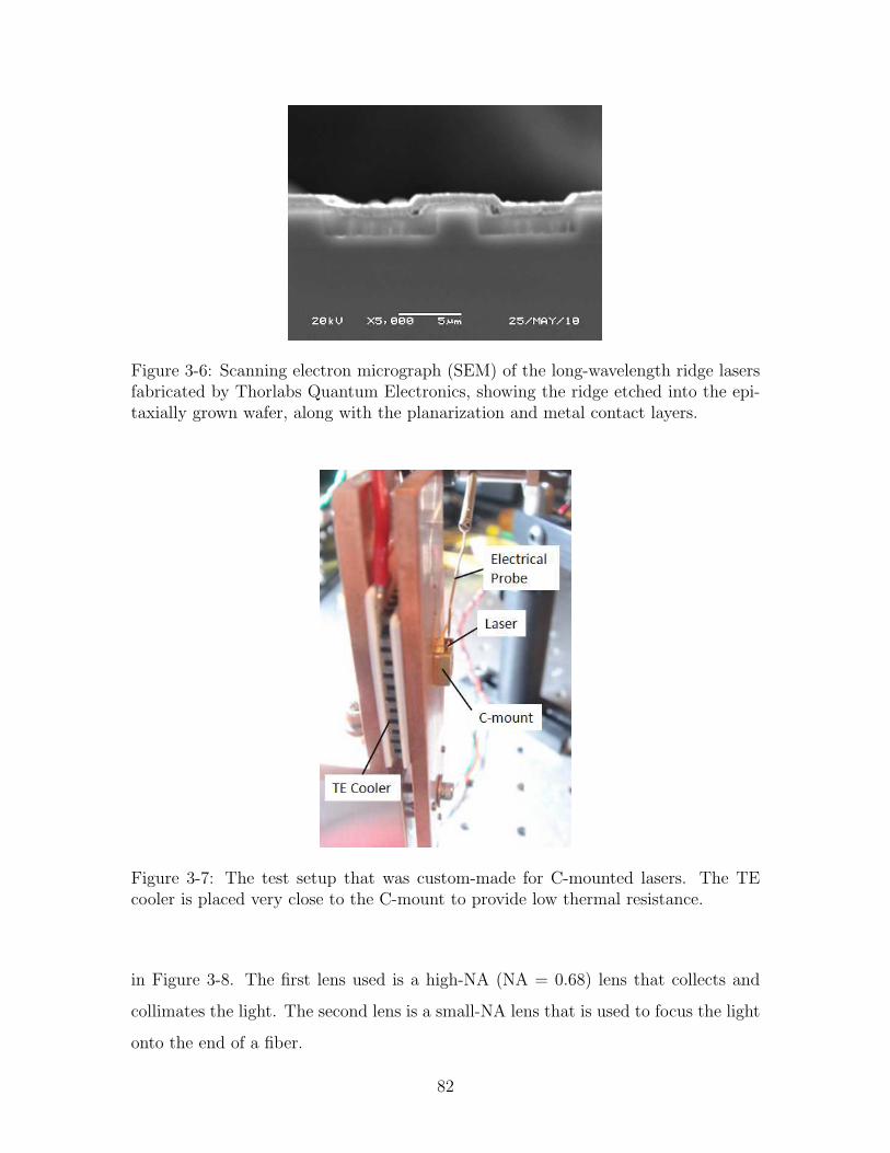
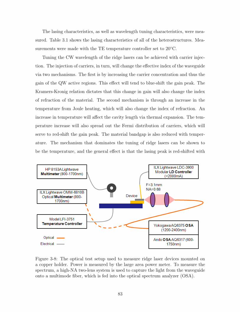
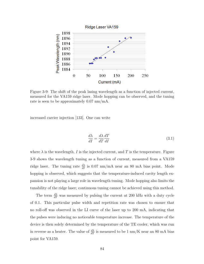
44
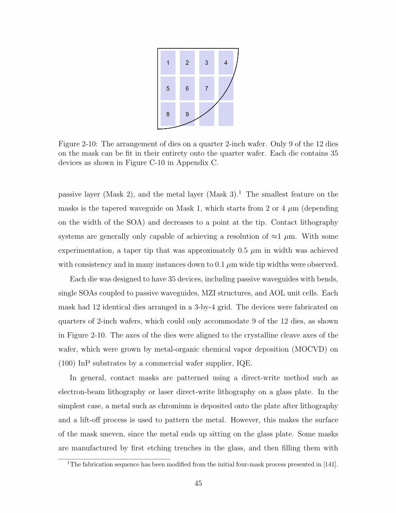
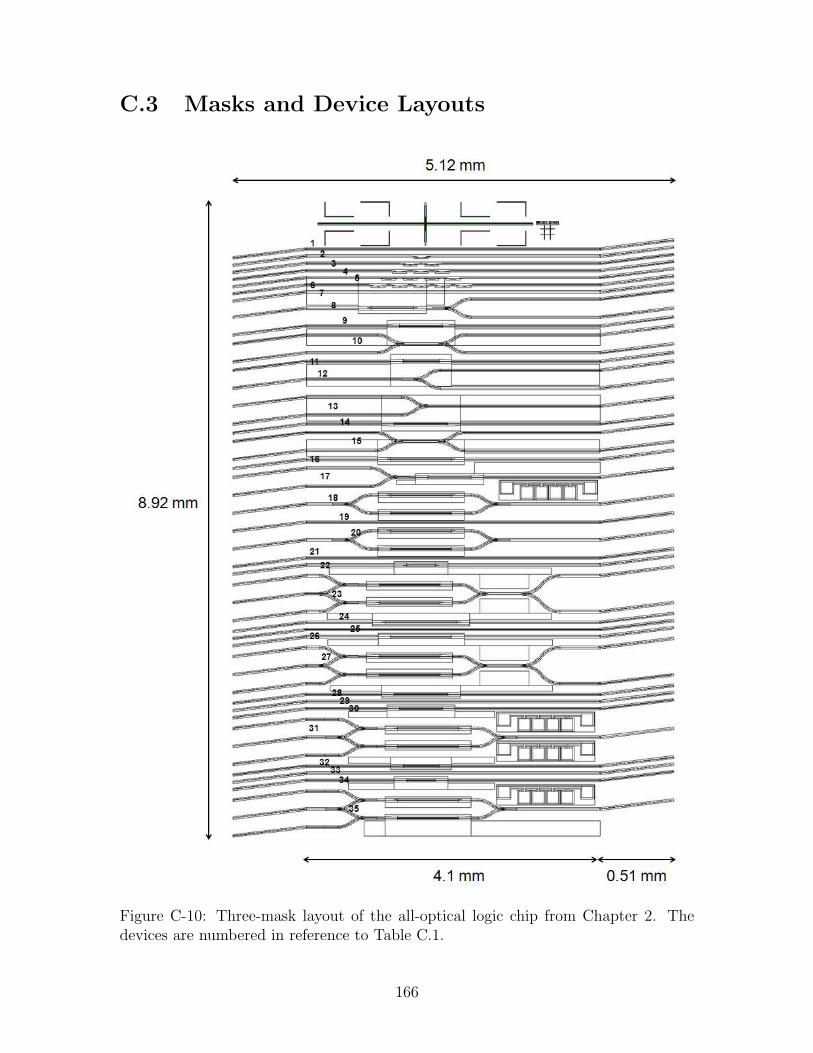
Figure 2-10: The arrangement of dies on a quarter 2-inch wafer. Only 9 of the 12 dieson the mask can be fit in their entirety onto the quarter wafer. Each die contains 35devices as shown in Figure C-10 in Appendix C.
passive layer (Mask 2), and the metal layer (Mask 3).1 The smallest feature on the
masks is the tapered waveguide on Mask 1, which starts from 2 or 4 µm (depending
on the width of the SOA) and decreases to a point at the tip. Contact lithography
systems are generally only capable of achieving a resolution of ≈1 µm. With some
experimentation, a taper tip that was approximately 0.5 µm in width was achieved
with consistency and in many instances down to 0.1 µm wide tip widths were observed.
Each die was designed to have 35 devices, including passive waveguides with bends,
single SOAs coupled to passive waveguides, MZI structures, and AOL unit cells. Each
mask had 12 identical dies arranged in a 3-by-4 grid. The devices were fabricated on
quarters of 2-inch wafers, which could only accommodate 9 of the 12 dies, as shown
in Figure 2-10. The axes of the dies were aligned to the crystalline cleave axes of the
wafer, which were grown by metal-organic chemical vapor deposition (MOCVD) on
(100) InP substrates by a commercial wafer supplier, IQE.
In general, contact masks are patterned using a direct-write method such as
electron-beam lithography or laser direct-write lithography on a glass plate. In the
simplest case, a metal such as chromium is deposited onto the plate after lithography
and a lift-off process is used to pattern the metal. However, this makes the surface
of the mask uneven, since the metal ends up sitting on the glass plate. Some masks
are manufactured by first etching trenches in the glass, and then filling them with
1The fabrication sequence has been modified from the initial four-mask process presented in [141].
45
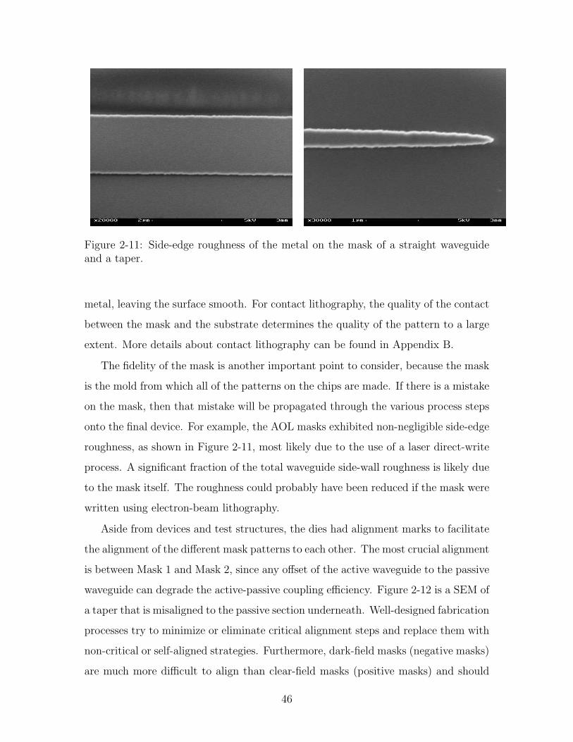
Figure 2-11: Side-edge roughness of the metal on the mask of a straight waveguideand a taper.
metal, leaving the surface smooth. For contact lithography, the quality of the contact
between the mask and the substrate determines the quality of the pattern to a large
extent. More details about contact lithography can be found in Appendix B.
The fidelity of the mask is another important point to consider, because the mask
is the mold from which all of the patterns on the chips are made. If there is a mistake
on the mask, then that mistake will be propagated through the various process steps
onto the final device. For example, the AOL masks exhibited non-negligible side-edge
roughness, as shown in Figure 2-11, most likely due to the use of a laser direct-write
process. A significant fraction of the total waveguide side-wall roughness is likely due
to the mask itself. The roughness could probably have been reduced if the mask were
written using electron-beam lithography.
Aside from devices and test structures, the dies had alignment marks to facilitate
the alignment of the different mask patterns to each other. The most crucial alignment
is between Mask 1 and Mask 2, since any offset of the active waveguide to the passive
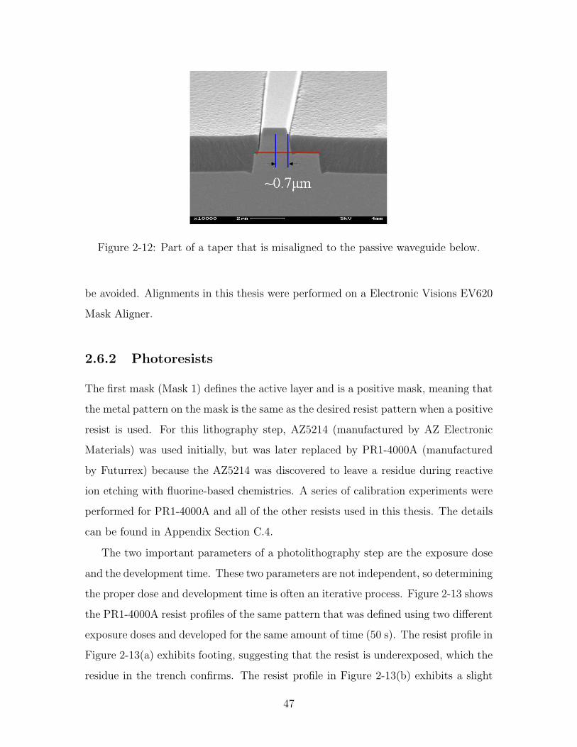
waveguide can degrade the active-passive coupling efficiency. Figure 2-12 is a SEM of
a taper that is misaligned to the passive section underneath. Well-designed fabrication
processes try to minimize or eliminate critical alignment steps and replace them with
non-critical or self-aligned strategies. Furthermore, dark-field masks (negative masks)
are much more difficult to align than clear-field masks (positive masks) and should
46
Figure 2-12: Part of a taper that is misaligned to the passive waveguide below.
be avoided. Alignments in this thesis were performed on a Electronic Visions EV620
Mask Aligner.
2.6.2 Photoresists
The first mask (Mask 1) defines the active layer and is a positive mask, meaning that
the metal pattern on the mask is the same as the desired resist pattern when a positive
resist is used. For this lithography step, AZ5214 (manufactured by AZ Electronic
Materials) was used initially, but was later replaced by PR1-4000A (manufactured
by Futurrex) because the AZ5214 was discovered to leave a residue during reactive
ion etching with fluorine-based chemistries. A series of calibration experiments were
performed for PR1-4000A and all of the other resists used in this thesis. The details
can be found in Appendix Section C.4.
The two important parameters of a photolithography step are the exposure dose
and the development time. These two parameters are not independent, so determining
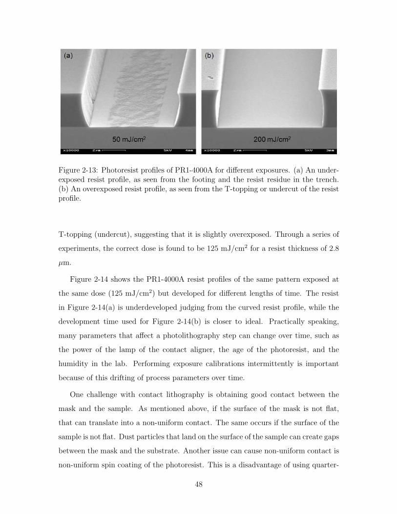
the proper dose and development time is often an iterative process. Figure 2-13 shows
the PR1-4000A resist profiles of the same pattern that was defined using two different
exposure doses and developed for the same amount of time (50 s). The resist profile in
Figure 2-13(a) exhibits footing, suggesting that the resist is underexposed, which the
residue in the trench confirms. The resist profile in Figure 2-13(b) exhibits a slight
47
Figure 2-13: Photoresist profiles of PR1-4000A for different exposures. (a) An under-exposed resist profile, as seen from the footing and the resist residue in the trench.(b) An overexposed resist profile, as seen from the T-topping or undercut of the resistprofile.
T-topping (undercut), suggesting that it is slightly overexposed. Through a series of
experiments, the correct dose is found to be 125 mJ/cm2 for a resist thickness of 2.8
µm.
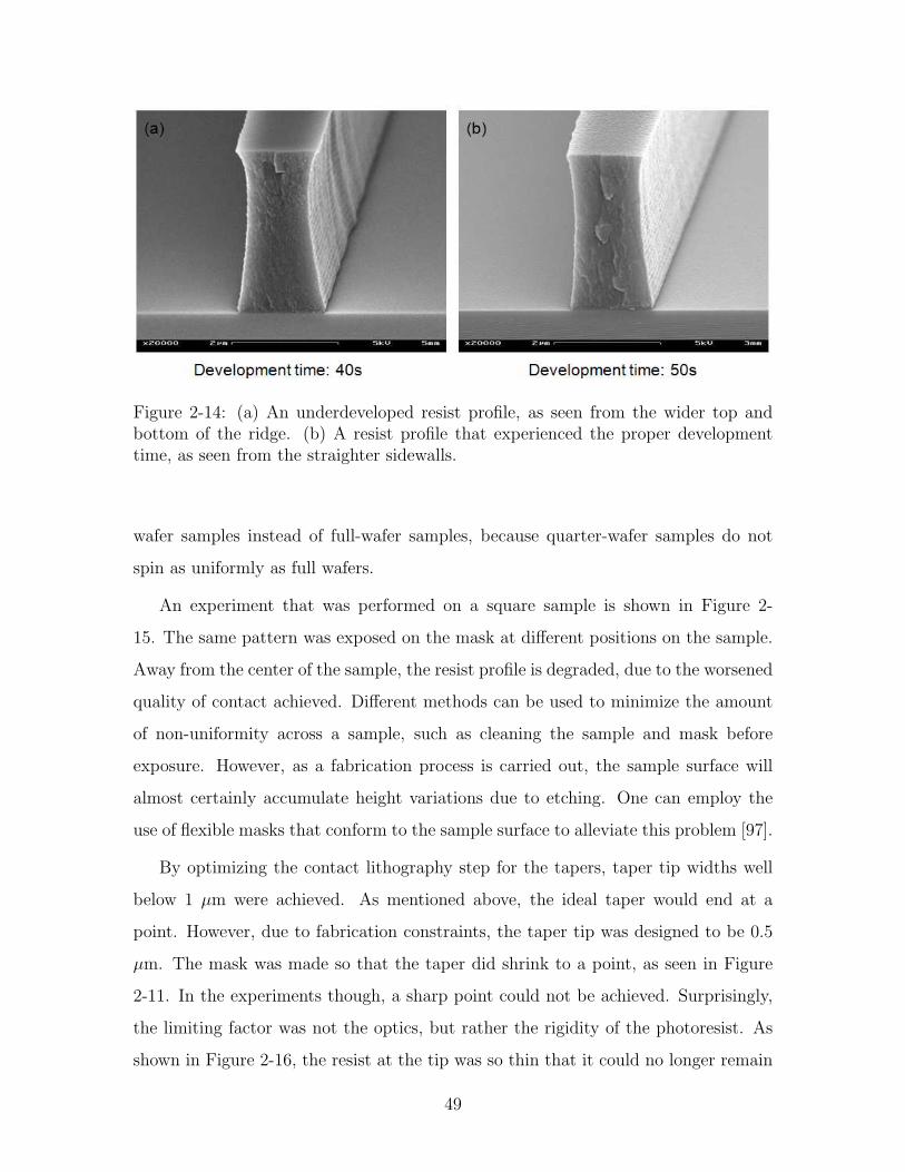
Figure 2-14 shows the PR1-4000A resist profiles of the same pattern exposed at
the same dose (125 mJ/cm2) but developed for different lengths of time. The resist
in Figure 2-14(a) is underdeveloped judging from the curved resist profile, while the
development time used for Figure 2-14(b) is closer to ideal. Practically speaking,
many parameters that affect a photolithography step can change over time, such as
the power of the lamp of the contact aligner, the age of the photoresist, and the
humidity in the lab. Performing exposure calibrations intermittently is important
because of this drifting of process parameters over time.
One challenge with contact lithography is obtaining good contact between the
mask and the sample. As mentioned above, if the surface of the mask is not flat,
that can translate into a non-uniform contact. The same occurs if the surface of the
sample is not flat. Dust particles that land on the surface of the sample can create gaps
between the mask and the substrate. Another issue can cause non-uniform contact is
non-uniform spin coating of the photoresist. This is a disadvantage of using quarter-
48
Figure 2-14: (a) An underdeveloped resist profile, as seen from the wider top andbottom of the ridge. (b) A resist profile that experienced the proper developmenttime, as seen from the straighter sidewalls.
wafer samples instead of full-wafer samples, because quarter-wafer samples do not
spin as uniformly as full wafers.
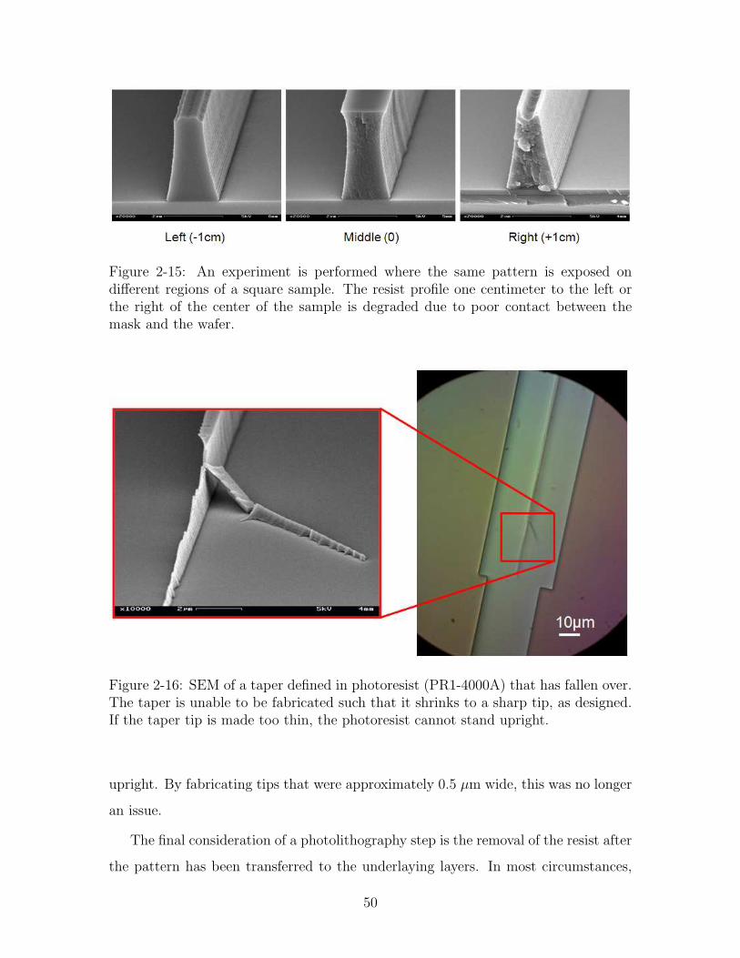
An experiment that was performed on a square sample is shown in Figure 2-
15. The same pattern was exposed on the mask at different positions on the sample.
Away from the center of the sample, the resist profile is degraded, due to the worsened
quality of contact achieved. Different methods can be used to minimize the amount
of non-uniformity across a sample, such as cleaning the sample and mask before
exposure. However, as a fabrication process is carried out, the sample surface will
almost certainly accumulate height variations due to etching. One can employ the
use of flexible masks that conform to the sample surface to alleviate this problem [97].
By optimizing the contact lithography step for the tapers, taper tip widths well
below 1 µm were achieved. As mentioned above, the ideal taper would end at a
point. However, due to fabrication constraints, the taper tip was designed to be 0.5
µm. The mask was made so that the taper did shrink to a point, as seen in Figure
2-11. In the experiments though, a sharp point could not be achieved. Surprisingly,
the limiting factor was not the optics, but rather the rigidity of the photoresist. As
shown in Figure 2-16, the resist at the tip was so thin that it could no longer remain
49
Figure 2-15: An experiment is performed where the same pattern is exposed ondifferent regions of a square sample. The resist profile one centimeter to the left orthe right of the center of the sample is degraded due to poor contact between themask and the wafer.
Figure 2-16: SEM of a taper defined in photoresist (PR1-4000A) that has fallen over.The taper is unable to be fabricated such that it shrinks to a sharp tip, as designed.If the taper tip is made too thin, the photoresist cannot stand upright.
upright. By fabricating tips that were approximately 0.5 µm wide, this was no longer
an issue.
The final consideration of a photolithography step is the removal of the resist after
the pattern has been transferred to the underlaying layers. In most circumstances,
50
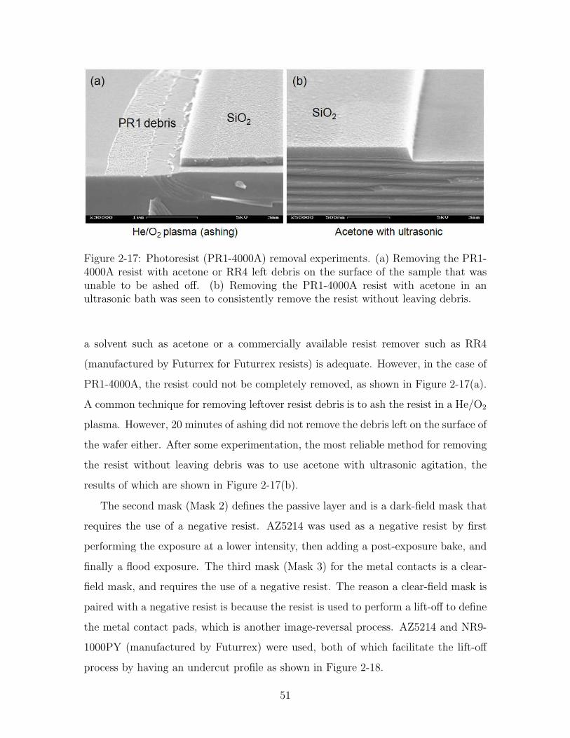
Figure 2-17: Photoresist (PR1-4000A) removal experiments. (a) Removing the PR1-4000A resist with acetone or RR4 left debris on the surface of the sample that wasunable to be ashed off. (b) Removing the PR1-4000A resist with acetone in anultrasonic bath was seen to consistently remove the resist without leaving debris.
a solvent such as acetone or a commercially available resist remover such as RR4
(manufactured by Futurrex for Futurrex resists) is adequate. However, in the case of
PR1-4000A, the resist could not be completely removed, as shown in Figure 2-17(a).
A common technique for removing leftover resist debris is to ash the resist in a He/O2
plasma. However, 20 minutes of ashing did not remove the debris left on the surface of
the wafer either. After some experimentation, the most reliable method for removing
the resist without leaving debris was to use acetone with ultrasonic agitation, the
results of which are shown in Figure 2-17(b).
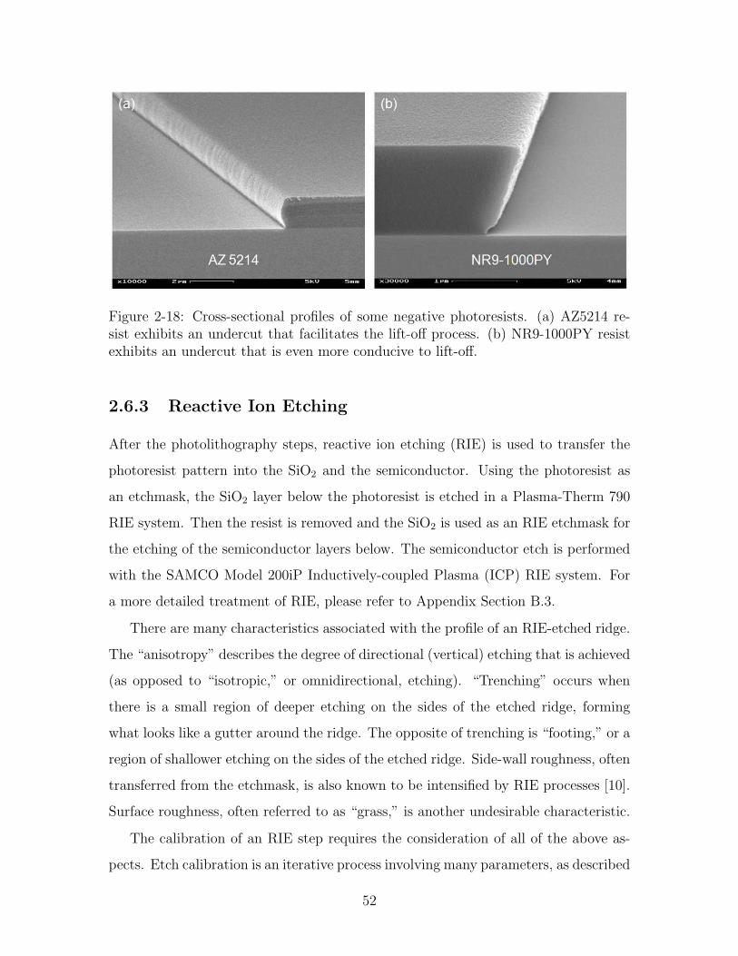
The second mask (Mask 2) defines the passive layer and is a dark-field mask that
requires the use of a negative resist. AZ5214 was used as a negative resist by first
performing the exposure at a lower intensity, then adding a post-exposure bake, and
finally a flood exposure. The third mask (Mask 3) for the metal contacts is a clear-
field mask, and requires the use of a negative resist. The reason a clear-field mask is
paired with a negative resist is because the resist is used to perform a lift-off to define
the metal contact pads, which is another image-reversal process. AZ5214 and NR9-
1000PY (manufactured by Futurrex) were used, both of which facilitate the lift-off
process by having an undercut profile as shown in Figure 2-18.
51
Figure 2-18: Cross-sectional profiles of some negative photoresists. (a) AZ5214 re-sist exhibits an undercut that facilitates the lift-off process. (b) NR9-1000PY resistexhibits an undercut that is even more conducive to lift-off.
2.6.3 Reactive Ion Etching
After the photolithography steps, reactive ion etching (RIE) is used to transfer the
photoresist pattern into the SiO2 and the semiconductor. Using the photoresist as
an etchmask, the SiO2 layer below the photoresist is etched in a Plasma-Therm 790
RIE system. Then the resist is removed and the SiO2 is used as an RIE etchmask for
the etching of the semiconductor layers below. The semiconductor etch is performed
with the SAMCO Model 200iP Inductively-coupled Plasma (ICP) RIE system. For
a more detailed treatment of RIE, please refer to Appendix Section B.3.
There are many characteristics associated with the profile of an RIE-etched ridge.
The “anisotropy” describes the degree of directional (vertical) etching that is achieved
(as opposed to “isotropic,” or omnidirectional, etching). “Trenching” occurs when
there is a small region of deeper etching on the sides of the etched ridge, forming
what looks like a gutter around the ridge. The opposite of trenching is “footing,” or a
region of shallower etching on the sides of the etched ridge. Side-wall roughness, often
transferred from the etchmask, is also known to be intensified by RIE processes [10].
Surface roughness, often referred to as “grass,” is another undesirable characteristic.
The calibration of an RIE step requires the consideration of all of the above as-
pects. Etch calibration is an iterative process involving many parameters, as described
52
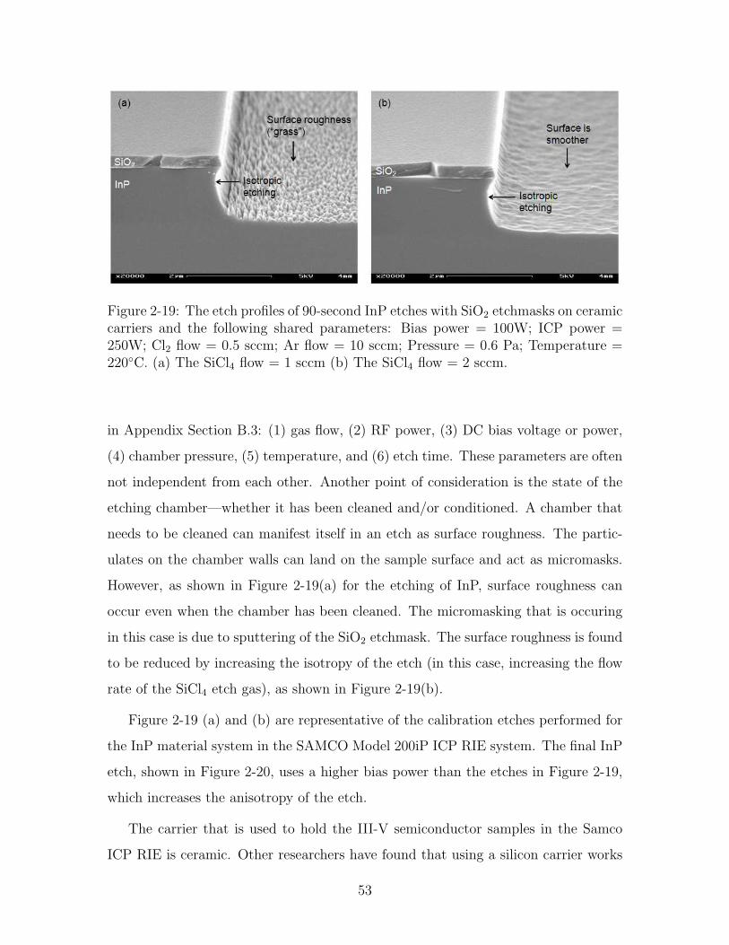
Figure 2-19: The etch profiles of 90-second InP etches with SiO2 etchmasks on ceramiccarriers and the following shared parameters: Bias power = 100W; ICP power =250W; Cl2 flow = 0.5 sccm; Ar flow = 10 sccm; Pressure = 0.6 Pa; Temperature =220C. (a) The SiCl4 flow = 1 sccm (b) The SiCl4 flow = 2 sccm.
in Appendix Section B.3: (1) gas flow, (2) RF power, (3) DC bias voltage or power,
(4) chamber pressure, (5) temperature, and (6) etch time. These parameters are often
not independent from each other. Another point of consideration is the state of the
etching chamber—whether it has been cleaned and/or conditioned. A chamber that
needs to be cleaned can manifest itself in an etch as surface roughness. The partic-
ulates on the chamber walls can land on the sample surface and act as micromasks.
However, as shown in Figure 2-19(a) for the etching of InP, surface roughness can
occur even when the chamber has been cleaned. The micromasking that is occuring
in this case is due to sputtering of the SiO2 etchmask. The surface roughness is found
to be reduced by increasing the isotropy of the etch (in this case, increasing the flow
rate of the SiCl4 etch gas), as shown in Figure 2-19(b).
Figure 2-19 (a) and (b) are representative of the calibration etches performed for
the InP material system in the SAMCO Model 200iP ICP RIE system. The final InP
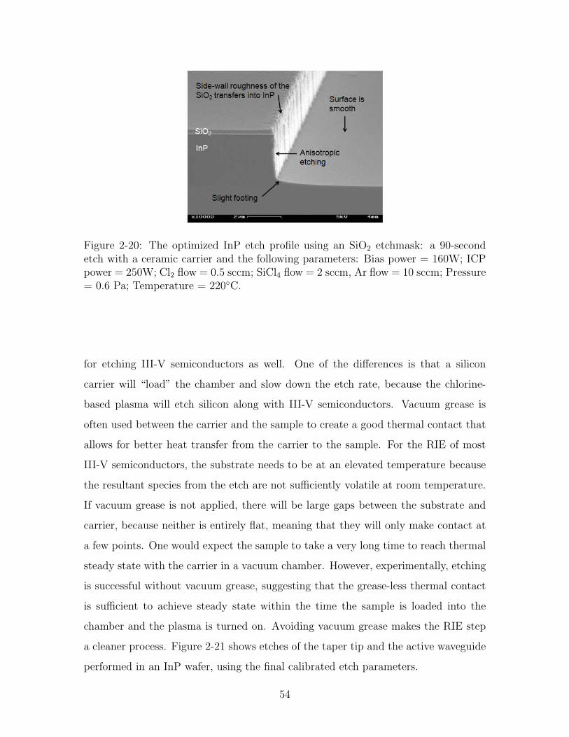
etch, shown in Figure 2-20, uses a higher bias power than the etches in Figure 2-19,
which increases the anisotropy of the etch.
The carrier that is used to hold the III-V semiconductor samples in the Samco
ICP RIE is ceramic. Other researchers have found that using a silicon carrier works
53
Figure 2-20: The optimized InP etch profile using an SiO2 etchmask: a 90-secondetch with a ceramic carrier and the following parameters: Bias power = 160W; ICPpower = 250W; Cl2 flow = 0.5 sccm; SiCl4 flow = 2 sccm, Ar flow = 10 sccm; Pressure= 0.6 Pa; Temperature = 220C.
for etching III-V semiconductors as well. One of the differences is that a silicon
carrier will “load” the chamber and slow down the etch rate, because the chlorine-
based plasma will etch silicon along with III-V semiconductors. Vacuum grease is
often used between the carrier and the sample to create a good thermal contact that
allows for better heat transfer from the carrier to the sample. For the RIE of most
III-V semiconductors, the substrate needs to be at an elevated temperature because
the resultant species from the etch are not sufficiently volatile at room temperature.
If vacuum grease is not applied, there will be large gaps between the substrate and
carrier, because neither is entirely flat, meaning that they will only make contact at
a few points. One would expect the sample to take a very long time to reach thermal
steady state with the carrier in a vacuum chamber. However, experimentally, etching
is successful without vacuum grease, suggesting that the grease-less thermal contact
is sufficient to achieve steady state within the time the sample is loaded into the
chamber and the plasma is turned on. Avoiding vacuum grease makes the RIE step
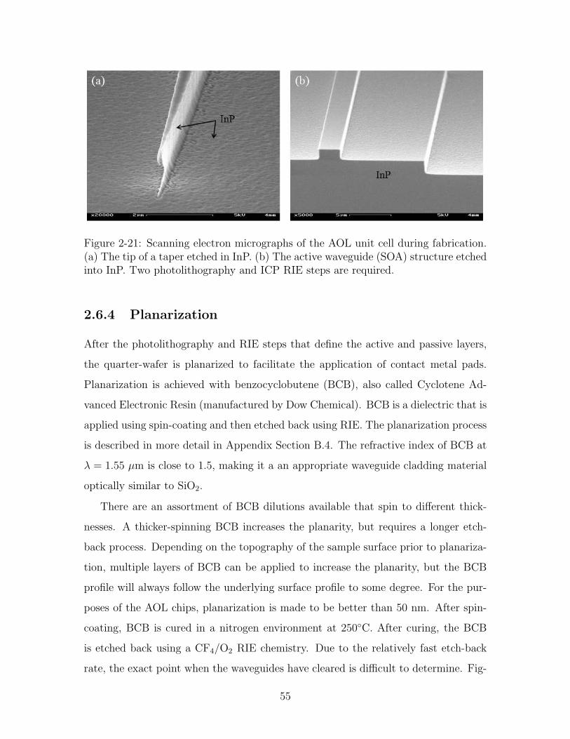
a cleaner process. Figure 2-21 shows etches of the taper tip and the active waveguide
performed in an InP wafer, using the final calibrated etch parameters.
54
Figure 2-21: Scanning electron micrographs of the AOL unit cell during fabrication.(a) The tip of a taper etched in InP. (b) The active waveguide (SOA) structure etchedinto InP. Two photolithography and ICP RIE steps are required.
2.6.4 Planarization
After the photolithography and RIE steps that define the active and passive layers,
the quarter-wafer is planarized to facilitate the application of contact metal pads.
Planarization is achieved with benzocyclobutene (BCB), also called Cyclotene Ad-
vanced Electronic Resin (manufactured by Dow Chemical). BCB is a dielectric that is
applied using spin-coating and then etched back using RIE. The planarization process
is described in more detail in Appendix Section B.4. The refractive index of BCB at
λ = 1.55 µm is close to 1.5, making it a an appropriate waveguide cladding material
optically similar to SiO2.
There are an assortment of BCB dilutions available that spin to different thick-
nesses. A thicker-spinning BCB increases the planarity, but requires a longer etch-
back process. Depending on the topography of the sample surface prior to planariza-
tion, multiple layers of BCB can be applied to increase the planarity, but the BCB
profile will always follow the underlying surface profile to some degree. For the pur-
poses of the AOL chips, planarization is made to be better than 50 nm. After spin-
coating, BCB is cured in a nitrogen environment at 250C. After curing, the BCB
is etched back using a CF4/O2 RIE chemistry. Due to the relatively fast etch-back
rate, the exact point when the waveguides have cleared is difficult to determine. Fig-
55
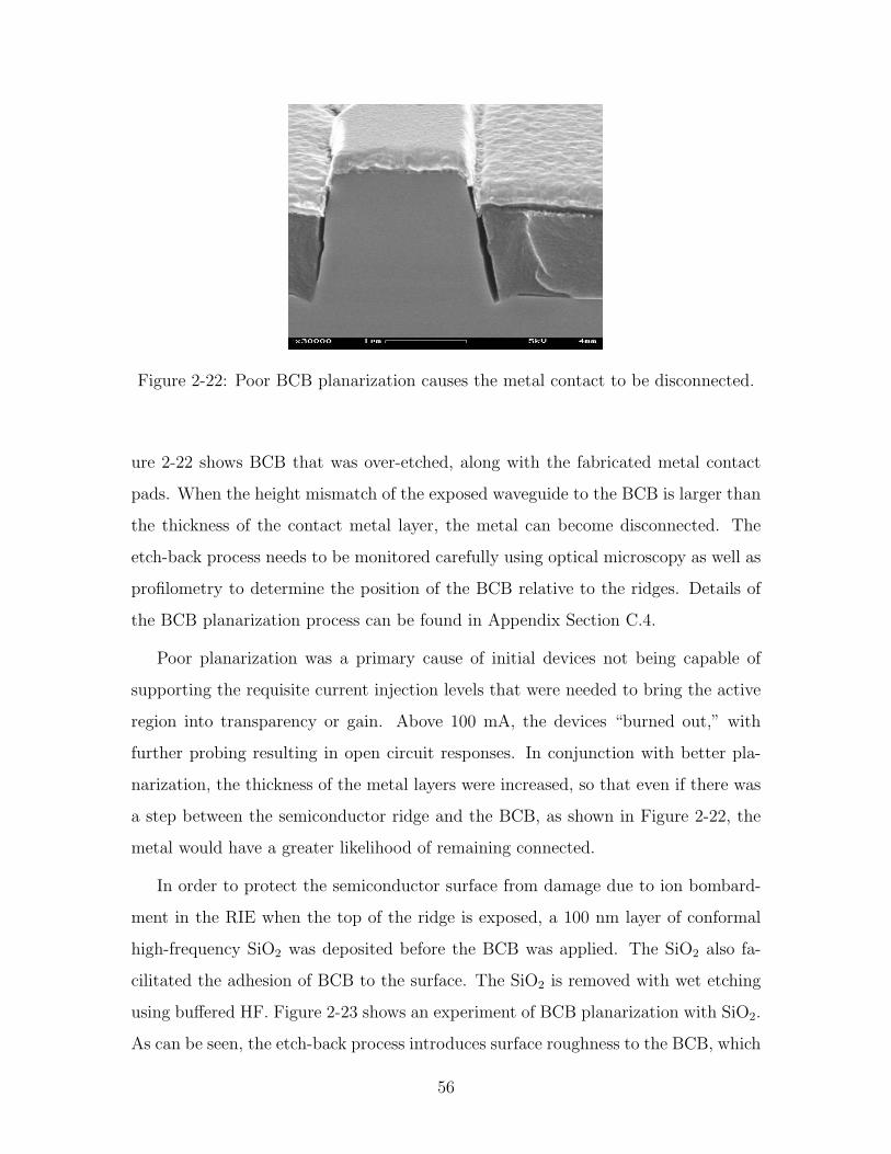
Figure 2-22: Poor BCB planarization causes the metal contact to be disconnected.
ure 2-22 shows BCB that was over-etched, along with the fabricated metal contact
pads. When the height mismatch of the exposed waveguide to the BCB is larger than
the thickness of the contact metal layer, the metal can become disconnected. The
etch-back process needs to be monitored carefully using optical microscopy as well as
profilometry to determine the position of the BCB relative to the ridges. Details of
the BCB planarization process can be found in Appendix Section C.4.
Poor planarization was a primary cause of initial devices not being capable of
supporting the requisite current injection levels that were needed to bring the active
region into transparency or gain. Above 100 mA, the devices “burned out,” with
further probing resulting in open circuit responses. In conjunction with better pla-
narization, the thickness of the metal layers were increased, so that even if there was
a step between the semiconductor ridge and the BCB, as shown in Figure 2-22, the
metal would have a greater likelihood of remaining connected.
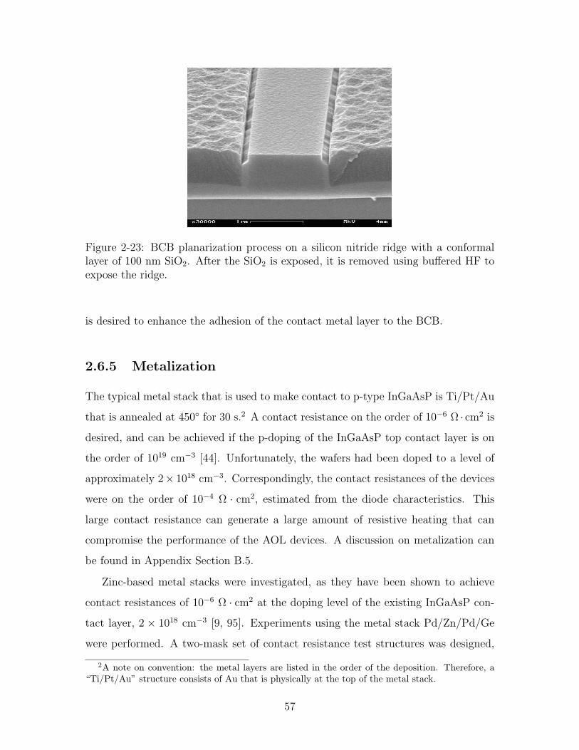
In order to protect the semiconductor surface from damage due to ion bombard-
ment in the RIE when the top of the ridge is exposed, a 100 nm layer of conformal
high-frequency SiO2 was deposited before the BCB was applied. The SiO2 also fa-
cilitated the adhesion of BCB to the surface. The SiO2 is removed with wet etching
using buffered HF. Figure 2-23 shows an experiment of BCB planarization with SiO2.
As can be seen, the etch-back process introduces surface roughness to the BCB, which
56
Figure 2-23: BCB planarization process on a silicon nitride ridge with a conformallayer of 100 nm SiO2. After the SiO2 is exposed, it is removed using buffered HF toexpose the ridge.
is desired to enhance the adhesion of the contact metal layer to the BCB.
2.6.5 Metalization
The typical metal stack that is used to make contact to p-type InGaAsP is Ti/Pt/Au
that is annealed at 450 for 30 s.2 A contact resistance on the order of 10−6 Ω · cm2 is
desired, and can be achieved if the p-doping of the InGaAsP top contact layer is on
the order of 1019 cm−3 [44]. Unfortunately, the wafers had been doped to a level of
approximately 2× 1018 cm−3. Correspondingly, the contact resistances of the devices
were on the order of 10−4 Ω · cm2, estimated from the diode characteristics. This
large contact resistance can generate a large amount of resistive heating that can
compromise the performance of the AOL devices. A discussion on metalization can
be found in Appendix Section B.5.
Zinc-based metal stacks were investigated, as they have been shown to achieve
contact resistances of 10−6 Ω · cm2 at the doping level of the existing InGaAsP con-
tact layer, 2 × 1018 cm−3 [9, 95]. Experiments using the metal stack Pd/Zn/Pd/Ge
were performed. A two-mask set of contact resistance test structures was designed,
2A note on convention: the metal layers are listed in the order of the deposition. Therefore, a“Ti/Pt/Au” structure consists of Au that is physically at the top of the metal stack.
57
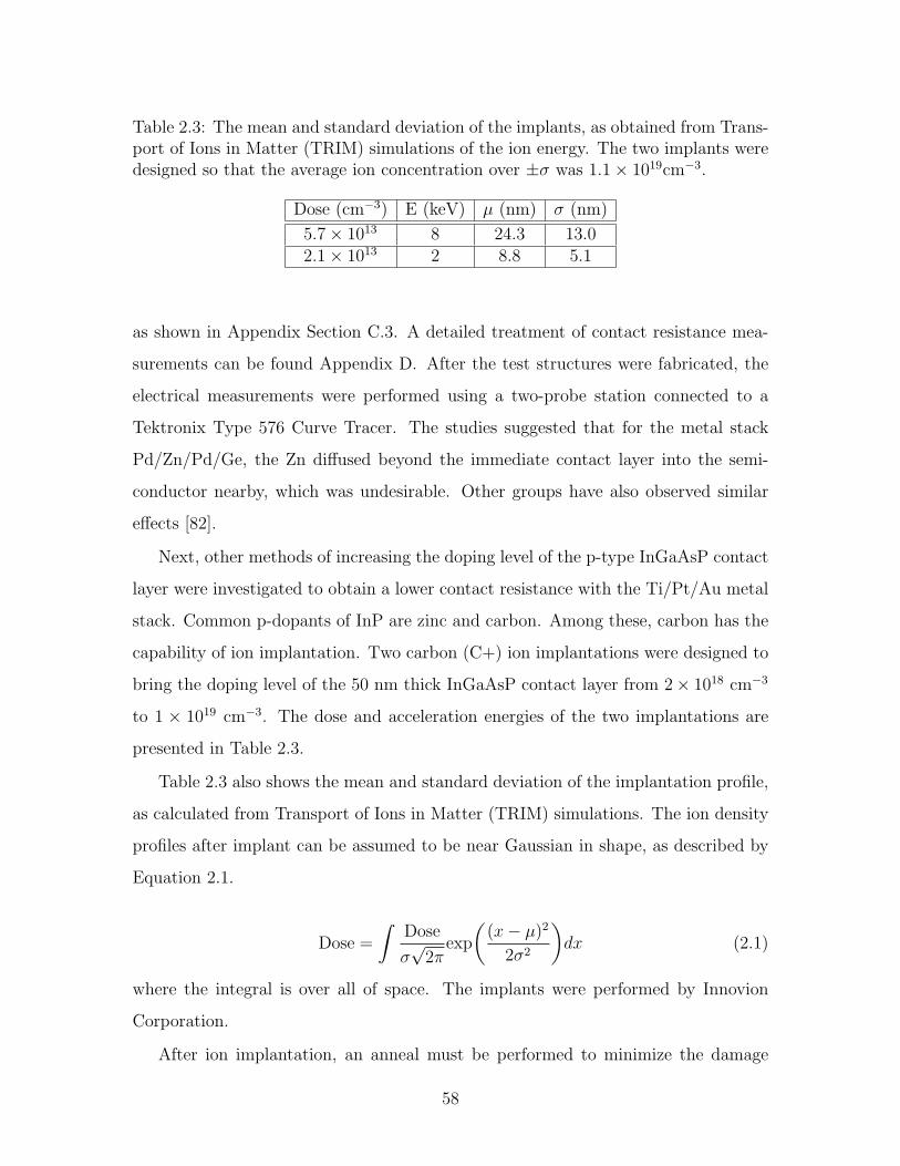
Table 2.3: The mean and standard deviation of the implants, as obtained from Trans-port of Ions in Matter (TRIM) simulations of the ion energy. The two implants weredesigned so that the average ion concentration over ±σ was 1.1× 1019cm−3.
Dose (cm−3) E (keV) µ (nm) σ (nm)
5.7× 10¹³ 8 24.3 13.02.1× 1013 2 8.8 5.1
as shown in Appendix Section C.3. A detailed treatment of contact resistance mea-
surements can be found Appendix D. After the test structures were fabricated, the
electrical measurements were performed using a two-probe station connected to a
Tektronix Type 576 Curve Tracer. The studies suggested that for the metal stack
Pd/Zn/Pd/Ge, the Zn diffused beyond the immediate contact layer into the semi-
conductor nearby, which was undesirable. Other groups have also observed similar
effects [82].
Next, other methods of increasing the doping level of the p-type InGaAsP contact
layer were investigated to obtain a lower contact resistance with the Ti/Pt/Au metal
stack. Common p-dopants of InP are zinc and carbon. Among these, carbon has the
capability of ion implantation. Two carbon (C+) ion implantations were designed to
bring the doping level of the 50 nm thick InGaAsP contact layer from 2× 1018 cm−3
to 1 × 1019 cm−3. The dose and acceleration energies of the two implantations are
presented in Table 2.3.
Table 2.3 also shows the mean and standard deviation of the implantation profile,
as calculated from Transport of Ions in Matter (TRIM) simulations. The ion density
profiles after implant can be assumed to be near Gaussian in shape, as described by
Equation 2.1.
Dose =
∫Dose
σ√
2πexp
((x− µ)2
2σ2
)dx (2.1)
where the integral is over all of space. The implants were performed by Innovion
Corporation.
After ion implantation, an anneal must be performed to minimize the damage
58
due to the ion bombardment of the substrate via recrystallization. If left unannealed,
the dangling bonds produced by the ion bombardment can introduce mid-gap states
that would degrade the efficiency of the device by providing nonradiative pathways
for recombination. The anneal process will also allow the carbon atoms to diffuse
beyond the Gaussian density profiles described by Equation 2.1, creating a more
uniform distribution. After experimenting with the anneal process, a final anneal of
750C for 60 s was seen to exhibit the lowest contact resistance. However, after the
fabrication of the devices, measurements were unsuccessful, most likely due to damage
still left in the contact layer even after the anneal was performed. At this time, effort
was shifted towards fabricating and characterizing devices with the original contact
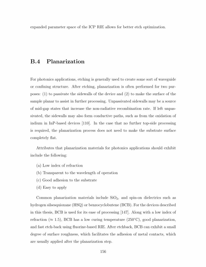
layer doping and the Ti/Pt/Au metal stack. Despite the higher contact resistance,
the devices operated properly as long as they received adequate cooling.
To facilitate heat dissipation, thick metal (on the order of 1 µm) was used for the
contact pads. Thicker metal also eases the electrical probing process and enhances
metal continuity across non-planar regions of the wafer. The initial method of metal
deposition was electron beam (e-beam) evaporation. While electron beam evapora-
tion can be used to deposit thick metal, it is expensive because it coats the entire
evaporation chamber with metal, most of which is wasted. Layers thicker than 200
nm were seldom deposited using e-beam evaporation. The more economical alterna-
tive is electroplating, which only deposits metal at the desired locations of the contact
pads.
Electron beam evaporation of 900 nm of metal was performed. The total metal
stack consisted of Ti/Pt/Au with thickness of 30/20/850 nm. A lift-off process was
performed using AZ5214 photoresist. A good rule of thumb for lift-off is that the
thickness of the metal should be at most 1/3 that of the photoresist. Thus, multi-
ple lift-off steps were required to create 900 nm thick metal pads. A technique for
multiple lift-off steps of the same metal contact pattern was developed. As shown in
Figure, 2-24, consecutive lift-off patterns should be intentionally misaligned so that at
the photoresist-metal boundary, the thickness of the metal is not augmented by the
previous deposition. Three liftoff steps of thicknesses 300 nm each were performed,
59
with intentional misalignments of approximately 15 µm.
Figure 2-24: Technique for the lift-off of multiple metal layers. (a) A perfectly alignedresist profile can create difficulty in the lift-off step because the solvent has difficultyaccessing the edge of the photoresist. (b) An intentionally misaligned resist profiledoes not have the difficulty with lift-off.
Electroplating was also performed on certain samples to create metal pads that
were 2 µm in thickness. Electroplating is a process in which the sample is immersed in
a solution of metal ions. The metal (in this case, Au) is moved by an electric field to
coat areas of the sample that are electrically conductive. Prior to electroplating, metal
pads consisting of Ti/Pt/Au at thicknesses of 30/20/70 nm were fabricated using e-
beam evaporation and a lift-off step. Next 80 nm of Au was e-beam evaporated over
the entire sample. Finally, a photolithography step was used to define the contact
pads once again. The thin (80 nm) Au seed layer ensures that all of the contact pads
are electrically connected. Next, electroplating is performed. The Au accumulates in
areas that are not covered by photoresist. Finally, the photoresist is removed (this is
not a lift-off step) and a short wet-etch removes the thin layer of Au that connects
the contact pads to make them electrically isolated. Figure 2-25 shows the results of
contacts created using electroplating.
2.6.6 Post-processing
One of the challenges of fabricating an integrated photonic circuit is the input and
output coupling of optical signals. Because the waveguides run along the plane of the
wafer, the most natural inputs and outputs occur at the edges of the chip. However,
even when cleaving along a crystalline plane of the semiconductor, smooth facets
60
Figure 2-25: Contact pads formed by Au electroplating. (a) Electroplated metalcontact pads (2 µm thick) are seen to hang off the edge of a cleaved sample. (b)Electroplated metal contact pads on a sample facilitated electrical probing becausethe probe tip can be pressed into the thick metal.
can be difficult to achieve. If a facet is scalloped or otherwise not smooth, input
and output coupling will be compromised by excess scattering. Vertical couplers
have been developed as a way to avoid this problem [131]. One of the methods that
is used to obtain consistently smooth facets is wafer thinning, or lapping. Typical
commercial III-V semiconductor wafers are approximately 350 µm thick. When the
wafer is reduced to 200 µm or thinner, cleaving along crystalline planes results in
consistently smooth facets. Thinning the wafer also reduces the resistance of the
substrate and provides better heat dissipation through the substrate.
The samples were lapped by hand using aluminum oxide grit to a thickness of 160
µm. For the lapping process, the samples were mounted top-side down with wax to
a cylindrically-shaped piece of glass, whose top surface is an optical flat. Details of
the lapping process can be found in Appendix Section C.4.
61
After lapping, with the sample still mounted to the optical flat, 20/60/30/200 nm
of Ge/Au/Ni/Au was evaporated onto the backside of the sample with a BOC Coating
Technology Temescal FCE-2500. Then 50/70/50 nm of Ti/Pt/Au was sputter-coated
onto the sample. A rapid thermal anneal (RTA) was then performed in a RTP-600XP
at approximately 440C for 30 s. Afterwards, the samples were unmounted and rinsed
with trichloroethylene (TCE).
The thinned quarter-wafers were cleaved using a Loomis LSD-100 scriber into the
individual dies. Then the dies were soldered onto a “dogbone” copper carrier using
indium foil. Prior to soldering, the copper carrier was also coated with Ti/Pt/Au
(thicknesses 50/70/50 nm) for matching the thermal coefficient of expansion to the
Ti/Pt/Au sputtered onto the backside of the device. If materials that are soldered
together have mismatched thermal coefficients of expansion, the connection can break
due to thermal cycling (operation) of the device [141].
2.7 Measurement
The 35 devices on each die include (1) passive waveguides, (2) passive waveguides
with bends, (3) passive waveguides with 50:50-split MMIs, (4) single SOAs coupled
to passive waveguides, (5) Mach-Zehnder interferometers (MZIs) with SOAs in each
arm, and (6) AOL unit cells. In this section, the characterization of each type of
structure is described, in order of complexity.
The AOL chips were soldered onto a copper “dog-bone” shaped mount, which was
then affixed to an actively-cooled copper block in the testing setup. The thermoelec-
tric (TE) cooler is set to a temperature of 15C as measured by a thermistor inserted
into a hole that is drilled into the copper block. When cooling to temperatures below
18C, one must be careful about condensation on the sample, which occurs when the
temperature of the device is lower than the dew point of the laboratory environment.3
Figure 2-26 is a photograph of an AOL chip under testing. Light is coupled into and
out of the device using tapered fibers that have a 4 µm spot size. Depending on the
3The dew point is directly related to the humidity and is reported by most weather sources.
62
Figure 2-26: Schematic of the optical setup used for making measurements of theAOL chip. Current (I1, I2) is injected into the devices through probes brought fromabove the chip into contact with the metal pads. Light is coupled into and out ofthe device with tapered fibers. A coupling loss of 7.6 dB is experienced per facet.The single-mode SMF-28 output fiber is either connected to an InGaAs detector oran OSA, and the input fiber is connected to a tunable laser source.
type of measurement, the current probes, I1 and I2, may or may not be turned on.
2.7.1 Passive Waveguides and Bends
The most important metric that describes the passive waveguide structures is the
propagation loss. One common method that is used to determine waveguide loss is
the cut-back method. However, as the cut-back method is irreversibly destructive,
a more gentle technique, the Hakki-Paoli method, was used [35]. The Hakki-Paoli
method can be used to measure propagation losses independent of coupling losses
into and out of the waveguide. The Hakki-Paoli method involves coupling light into
the waveguide and varying its wavelength while measuring the transmission through
the waveguide. As a function of wavelength, the transmission is oscillatory, corre-
sponding to constructive and destructive interference between the reflected waves in
the resonator created by the cleaved mirror facets. The values of the maximum and
minimum transmitted powers depend only on the loss, reflectivities, and length of the
waveguide. Thus, the total loss of the waveguide can be determined from the output
63
Figure 2-27: SEM of passive waveguide structures with different numbers of bends.A single bend is defined as a single “S” shape.
powers, reflectivities, and length:
α =1
Lln
(√Pmax +
√Pmin√
Pmax −√
Pmin
)+
1
2Lln(R1R2) (2.2)
where α is the power loss coefficient. In the measurements, Pmax and Pmin are values
averaged over λ = 1549 and 1550.5 nm, R1 = R2 = 0.272 (calculated assuming
an effective index of 3.18), and L ≈ 3.5 mm for the particular chip. The passive
waveguides were designed to have outputs that are at a 7 angle with respect to the
cleaved facets to minimize reflections. However, because of initial difficulties coupling
light into and out of angled facets, the dies were cleaved with straight facets. The
passive waveguide loss was found to be 0.95 cm−1 or 4.1 dB/cm [137].
The AOL unit cell employs the use of passive waveguide bends. The larger bends
have radii of roughly 330 µm and the smaller bends have radii of roughly 296 µm. On
the dies, there are passive waveguides that have 2, 4, 6, and 8 bends that are designed
to help characterize the bending losses. The bends for the test structures, depicted in
Figure 2-27, have radii of roughly 285 µm, which means that any bending loss values
obtained from these devices will be an upper bound on the loss of the actual bends
that are used in the AOL unit cell. Using the Hakki-Paoli method, a bending loss of
64
1.17 dB per bend, or 0.75 dB per radian, was measured for the test structures. The
definition of a single bend is shown in Figure 2-27.
2.7.2 Single SOAs
With straight cleaved facets, the single SOAs that were coupled to passive waveguides
behaved as diode lasers. Figure 2-28(a) shows the lasing spectrum of an SOA (with
dimensions 850 µm × 4 µm) for different levels of current injection. The lasing
peak is seen to be red-shifted for increased current levels due to heating. The lasing
wavelength is between 1575 and 1580 nm. Figure 2-28(b) shows the I-L curve for the
same device. The threshold current is 210 mA and a peak output power of 2.5 mW
is achieved at 400 mA. For higher current levels, the power decreases due to heating.
To make the device into a single-pass SOA rather than a laser, the straight-cleaved
facets were anti-reflective (AR) coated. The fact that the same device was charac-
terized with and without reflective facets yielded a unique opportunity to determine
the tapered fiber coupling losses. Figure 2-29(a) depicts the laser structure, which
consists of an active waveguide (SOA) coupled via the adiabatic taper to passive
Figure 2-28: Measurements of a straight-cleaved 850 µm × 4 µm laser (before thefacets are AR coated). (a) The lasing spectrum for different current injection levels.(b) The I-L curve for the same device. The threshold current is 210 mA.
65
Figure 2-29: Schematic of the measurement of tapered fiber coupling losses. (a)Before AR coating: the taper-active-taper gain at Ith = 210 mA can be calculatedsince the round trip gain is known to be 0 dB. (b) After AR coating: the taperedfiber coupling loss can be calculated from a single-pass measurement since the taper-active-taper gain at I = 210 mA is unchanged.
waveguides on either end. The passive waveguide loss and the as-cleaved facet losses
are known. Thus, at threshold (210 mA), the gain of the taper-active-taper region
can be calculated, because the round-trip gain is known to be 0 dB.
After the application of the AR coating, a single-pass measurement can be made
at a wavelength of 1575 nm with I = 210 mA using the tapered fibers, as shown in
Figure 2-29(b). AR coating the facets does not affect the taper-active-taper gain of
the device. Thus, at I = 210 mA, the taper-active-taper gain is the same as before
AR coating took place. With all other losses known, the tapered fiber coupling loss
is calculated to be 7.6 dB per facet. This value is large due to the mismatch between
the passive waveguide mode, which is elongated (the passive waveguide is 4 µm wide
and 1 µm tall), and the symmetric focal spot of the tapered fiber.
Once the tapered fiber coupling losses were determined, the total taper-active-
66
Figure 2-30: Total gain or loss of the taper-active-taper region as a function of currentfor a wavelength of 1575 nm. The line is drawn to guide the eye.
taper gain at λ = 1575 nm could be found for different levels of current injection, as
shown in Figure 2-30. The gain region is seen to achieve transparency at I = 130
mA. The lasing threshold occurs at I = 210 mA when the gain is able to offset the
passive waveguide and mirror losses.
The same device is measured for its amplified spontaneous emission (ASE) spec-
trum. As shown in Figure 2-31, the ASE peak blueshifts for increasing current in-
jection up to approximately 300 mA. This blueshift is due to the bandfilling with
increased carrier concentration levels. Above 300 mA, the ASE peak redshifts due
to heating. The ASE spectrum is directly related to the gain spectrum of the active
materials [22].
2.7.3 Mach-Zehnder Interferometers
After characterizing single SOAs, the double SOAs arranged in the MZIs were char-
acterized. First, the MMI splitters were visually determined to provide close to 50-50
splitting [137]. The exact insertion loss of the MMI splitters were not measured be-
cause the important aspect of the MMI is to provide balanced splitting. Any losses
due to the MMI can be compensated for by the gain of the device.
67
Figure 2-31: The ASE spectrum of the 850 µm × 4 µm SOA for different currentinjection levels. For lower current levels, bandfilling causes the ASE peak to blueshift,and for high current levels, the ASE peak is redshifted due to heating.
Figure 2-32: The 2D bias scan in which the constructive and destructive interferenceof the MZI can be observed. (a) The 2D bias scan on a linear scale of throughputpower. (b) The 2D bias scan on a log scale.
Next, a bias scan is performed on the MZI to characterize the interference between
the two arms. A bias scan is a two-dimensional sweep of the DC current that is in-
jected into each SOA arm of the MZI while measuring the power throughput. A great
68
Figure 2-33: Measurement setup for the bias scan.
method for visualizing the bias scan is a 2D color plot that depicts the interference
between the two MZI arms, as shown in Figure 2-32. The bias scan derives its name
from the information that it provides on how to DC-bias the MZI arms for all-optical
logic operation.
Figure 2-33 shows a schematic of the measurement setup that was used to perform
the bias scan. The measurement system employs much of the same testing equipment
that was used to make the other measurements. The ILX current driver is controlled
by a Labview program to step the current from 0 to 500 mA in increments of 10
mA. The signal generator produces a sawtooth modulation signal that modulates the
Newport current driver output from 0 to 500 mA and back down in a sawtooth fashion.
The output is bandpass filtered to remove unwanted ASE before it is detected by the
InGaAs detector. The detector output voltage signal is fed into the oscilloscope and
is captured by the Labview program. The voltage is converted to optical power via
a conversion that was calibrated using an optical spectrum analyzer (OSA). Lowpass
filtering is performed in software to remove high frequency noise.
The resulting bias scan for a MZI with 850 µm × 4 µm SOAs is shown in Fig-
69
ure 2-32. The fringes correspond to bias points where constructive and destructive
interference occurs between the arms of the MZI. The dark region in the lower left of
the plot represents current levels that are inadequate to bring the SOAs past trans-
parency. For AOL operation, the SOAs should be biased for constructive interference.
For example, (I1, I2) = (300 mA, 400 mA) could be a potentially optimal point to bias
the SOAs. If used as a carrier injection modulator, the device exhibits an “Iπ” (anal-
ogous to Vπ) of approximately 50 mA at bias levels near the diode threshold. The
extinction ratio is approximately 20 dB.
2.8 Conclusion
All-optical logic has the potential to transform telecommunications and beyond. One
key component to the widespread adoption of AOL technology is integration. In this
chapter, the design of an integrated AOL unit cell that is based on an MZI structure
with electrically-pumped SOAs as nonlinear elements was presented. Targeted for
operation at the primary telecommunications wavelength of 1550 nm, the device was
modeled and fabricated in the InP-based material system. The fabricated devices
were then characterized. The operation of dilute active and passive waveguides,
bends, and MMIs were successfully demonstrated. Vertical passive-active coupling via
the asymmetric twin waveguide technique was also achieved. Finally, the static bias
scan was used to characterize the MZI, successfully demonstrating carrier-dependent
optical interference.
Future work includes the successful fabrication of AOL unit cells using quantum
dot active materials. Quantum dot materials can provide faster carrier recovery, which
could allow the current AOL unit cell design to achieve bit rates of 100 Gb/s or higher.
Demonstrations of pulsed signal switching with the AOL unit cells as well as cascaded
AOL unit cells performing different logic functions will also be investigated.
70
Chapter 3
Ridge Lasers
Ridge lasers are widely used in industry and research because they are one of the
most basic integrated semiconductor devices to design, fabricate, and characterize.
Consisting simply of a straight ridge waveguide with cleaved facet mirrors and a metal
contact, ridge lasers are quite tolerant to fabrication nonidealities such as alignment
and etching errors, making them an excellent proof-of-concept or diagnostic for novel
materials and more complicated devices. In addition, the packaging of ridge lasers has
become an industry standard, because III-V semiconductor diode lasers are preferred
nowadays to gas or solid state lasers in a variety of applications mainly due to their
being more compact, efficient, reliable and potentially inexpensive. In this chapter,
ridge lasers are utilized to investigate two material systems: InAs quantum dots
emitting at 1.5 µm, and strained InGaAs quantum wells (QWs) emitting at 1.6–2.0
µm.
3.1 Quantum Dot Lasers
Quantum dot (QD) lasers and amplifiers at 1.5µm have a broad range of potential
benefits for fiber-optic telecommunications applications. Quantum dots confine elec-
trons in three dimensions, creating a 3D potential well that “squeezes” the electronic
energy levels into atomic-like quantized steps. The energy level spacings depend on
the size of the QD, which can be made to have only a few bound energy levels. One
71
of the benefits of having only a few energy levels (sometimes only one or two) is that
fewer carriers are required to achieve population inversion, thus providing a lower
Ith than quantum well or bulk structures. Furthermore, the emission wavelength is
more stable to temperature changes, thus providing a higher T0 than quantum well
or bulk structures [13]. Other benefits of QD lasers include lower chirp and broader
gain spectrum for wavelength tuning or mode-locking. Quantum dot SOAs are also
expected to have lower noise figure and faster dynamic response times [55].
Self-assembled quantum dots that are grown by molecular beam epitaxy (MBE)
or metal-organic chemical vapor deposition (MOCVD) have been studied for the
fiber-optic telecommunications wavelengths of 1.3 µm and 1.55 µm. The term “self-
assembled” is used because a lattice mismatch is intentionally introduced between
the QD layer and the semiconductor it is residing on (often called the wetting layer)
so that the QD layer will form islands rather than become a continuous film, in order
to minimize the energy. Although called quantum dots, they are usually not round,
but are wider than they are tall as shown in Figure 3-1. Chemically synthesized QDs
on the other hand, such as CdSe QDs, often do resemble dots [17].
Indium Arsenide is a common semiconductor that is used to make QDs for the
telecommunications wavelengths. InAs has a bandgap of 0.354 eV, which translates
into a wavelength of 3.5 µm. However, in the form of a QD, the InAs energy levels
provide gain at 1.3 - 1.5 µm. In fact, 1.3 µm wavelength InAs-on-GaAs QD lasers
and SOAs are already quite mature [56, 121]. On the other hand, the operating
wavelength of 1.55 µm has been a more challenging domain. Some of the first 1.55-
µm-emitting QDs were also grown on GaAs. InGaAs and GaInNAs QDs on GaAs,
as well as InAs QDs on GaAs with an InGaAs strain-reducing layer were achieved
towards the last few years of the millennium [98, 112, 126]. Later, InAs QDs that were
grown on (311)B InP substrates that emitted at 1.55 µm were successfully measured
[99]. However, the (311)B InP substrate is less economical and fabrication-friendly
than the (100) InP substrate, and 1.5-µm-emitting InAs QDs that are grown on (100)
InP have been successfully grown on InGaAsP wetting layers or in InGaAsP QWs
(also called dots-in-a-well or DWELL) [55, 148, 7, 57]. Others have used InGaAlAs
72
wetting layers or grown InAs QDs directly on InP to achieve 1.5 µm emission [47, 71].
Our goal was to make a first pass on growing InAs QDs on (100) InP substrates,
and to characterize the emission of the QDs by fabrication of ridge lasers and by mea-
suring their electroluminescence. Two heterostructures were grown using MBE: one
consisting of quantum dots and the other of quantum dashes, which are effectively just
elongated quantum dots. A quantum well heterostructure was also grown for diagnos-
tic purposes. The photoluminescence of the gain materials for each heterostructure
was confirmed to have an emission range near 1.5 µm.
3.1.1 Epitaxial Structure
The epitaxial structure of the quantum dot, quantum dash, and quantum well het-
erostructures can be found in Appendix Section C.1. The QD heterostructure (VA117)
consists of four layers of 0.75 nm InAs on 2 nm of In0.5Ga0.4Al0.1As wetting layer, on
top of In0.75Ga0.25As0.55P0.45, and capped with 8 nm of In0.5Ga0.4Al0.1As. The quan-
tum dash heterostructure (VA118) consists of four layers of 0.9 nm InAs on 20 nm of
In0.8Ga0.2As0.46P0.54. The quantum well heterostructure (VA96) was grown with four
In0.54Ga0.46As quantum wells. A capping layer of 700 nm of InP was placed on top
of the gain layers to separate the mode from the metal contact, which is placed on
the very top of the structure. For VA117 and VA118, a thin layer of InGaAlAs was
grown in the middle of the InP cap layer to serve as a wet etch stop.
An atomic force microscope (AFM) image of the InAs quantum dot layer is shown
in Figure 3-1. The quantum dot density is measured to be 6 dots/µm2 per layer. A
total of four layers was grown, resulting in an effective dot density of 24 dots/µm2.
This dot density is too low to provide the requisite gain for lasing; in general the
density for room-temperature continuous-wave (CW) lasing needs to be at least ≈ 102
µm2 [55]. These results were later confirmed by the devices that we fabricated at MIT
as well as devices fabricated by Thorlabs Quantum Electronics (formerly Covega
Technology). In fact, the dot density of VA117 is in the range for which single-dot
experiments have been reported [6].
73
Figure 3-1: Atomic force microscope images of InAs quantum dots. (a) AFM imageof a 5 by 5 µm portion of the surface of VA159. The density is 6 dots/µm2, whichis too low to provide the gain required for lasing but can be utilized for single-dotemission experiments. (b) Angled AFM image of a magnified portion of the surface,showing the shape of the dots. The dots are about 10 nm tall on average and take anelongated shape of approximately 30 nm in width and 80 nm in length on average.
3.1.2 Fabrication
Ridge waveguides were fabricated using the quantum dot, quantum dash, and quan-
tum well heterostructures. The fabrication procedure for the ridge waveguides is
given in Figure 3-2. The methods that are used are mostly identical to the fabrica-
tion steps found in the all-optical logic process of Section 2.6. The only difference is
in the etching of the semiconductor layers.
Due to laboratory constraints, we were unable to utilize the SiCl4-based ICP RIE
process that was developed in Section 2.6 for the fabrication of these ridge waveguides.
Two methods of etching were investigated: (1) wet etching and (2) ICP reactive ion
etching with BCl3.
Wet etching of III-V semiconductors in the fabrication of photonic devices is gen-
erally avoided because the isotropic nature of the wet etch results in structures that
have curved sidewalls, which are difficult to model and introduces extra variables into
processes that are generally very complicated already. However, there are methods of
74
Figure 3-2: Process flow for the quantum dot and quantum dash ridge lasers.
75
making wet etches more anisotropic. In etch systems using HCl (which etches InP, for
example), weak acids such as phosphoric acid or acetic acid can be used to make the
etch more anisotopic [38]. Furthermore, one of the advantages of wet etch systems
for III-V semiconductors is that there are many options for selective etching. Contin-
uing with the example of HCl, scientists have discovered that the etch has selectivity
greater than 106 to In0.53Ga0.47As with respect to InP [104]. The InGaAlAs etch stop
layer found in VA117 and VA118 has low Al content and was seen to perform as an
effective etch stop in an etch consisting of HCl:H3PO4:H2O (1:1:10). On the other
hand, if one wanted to selectively etch In0.53Ga0.47As, while using InP as an etch
stop, a combination of citric acid and hydrogen peroxide has been shown to exhibit
a selectivity of 470 [27].
Experiments were also performed in the ICP RIE using BCl3 as the primary etch
gas. Figure 3-3 shows the most optimal BCl3 etch achieved. The surface is seen to
exhibit some roughness. However, because the waveguide mode is situated relatively
far from the surface, the roughness should contribute negligibly to the scattering loss
of the waveguide. Finally, the dry-etch method was chosen for its superior anisotropy
and ability of obtaining a deeper etch.
Figure 3-3: ICP RIE etching of InP using a BCl3 etch recipe. (a) 3-minute etch of InP(details of the etch can be found in Section C.4). (b) At greater magnification, thesurface exhibits roughness and there is a trench along the side of the ridge. Becausethe mode is expected to be situated below the surface, these features will not causeexcessive scattering losses.
76
Ridge waveguides ranging from 1 µm to 30 µm in width, arranged parallel to each
other with a period of 160 µm were fabricated using contact lithography. With a
resolution of ≈1 µm, contact lithography was empirically observed to reliably pattern
waveguides that were wider than 2 µm. Waveguides narrower than 2 µm were too close
to the resolution limit to be patterned reliably in practice. The ridges were etched to
a depth of 2.2 µm, making them multimode waveguides. The top Ti/Pt/Au metal
contact pads were 128 µm wide and separated by 32 µm.
3.1.3 Measurement and Conclusion
Electroluminescence (EL) spectra were measured from the fabricated waveguides, as
depicted in Figure 3-4. Both the quantum dot and quantum dash lasers exhibited
gain in the 1.4 µm to 1.5 µm range. The emission spectrum can be seen to be quite
broad, a feature of a QD gain region that results from the nonuniform dot sizes. The
measurements were performed with the thermoelectric (TE) temperature controller
set to 15C.
Figure 3-4: The electroluminescence spectra of InAs quantum dash and quantum dotmaterials. (a) The EL spectrum of the quantum dash material from waveguides withdifferent ridge dimensions. The emission is seen to be centered around 1400 nm. (b)The EL spectrum of the quantum dot material from waveguides with different ridgedimensions. The emission is seen to be centered around 1450 nm.
77
The densities of the dots and dashes were not high enough to provide enough
gain to offset the losses of the ridge waveguide and cleaved-facet mirrors. However,
the ridges fabricated from the quantum well heterostructure (VA96) by Thorlabs
Quantum Electronics did achieve CW lasing at 1.655 µm with 10 mW (at 500 mA)
output power, Ith = 110 mA, and differential efficiency η = 0.03 mW/mA.
These experiments provide an understanding of the QD material characteristics
from our MBE system. Future work includes the growth of higher-density QD mate-
rial by changing the MBE growth conditions, as well as increasing the number of QD
layers that are grown in a single device. Additionally, investigations into single-dot
emission can be performed on the lower-density QD material. Quantum dot gain
materials can also be used in all-optical logic gates to provide faster recovery times,
and hence, faster bit-rates (>100 Gbit/s). Quantum dot gain material at 1.5 µm will
continue to be an interesting area of research due to its wide range of applications.
3.2 Mid-infrared Lasers
The wavelength range between 1.7 µm and 5 µm is an important part of the infrared
spectrum that is not well-investigated. Unlike 1.3 µm and 1.5 µm wavelengths, the
study of which has been driven by fiber-optic telecommunications applications, the
longer wavelengths currently do not have readily available commercial laser sources,
amplifiers, or detectors. This part of the infrared spectrum lies at the tenuous bound-
ary between what most scientists classify as “near-infrared” and “mid-infrared” (mid-
IR). Part of this wavelength range is also often referred to as “short-wave infrared”.
Without dwelling too much on semantics, for the remainder of this thesis, the 1.7–5
µm wavelengths will be referred to as “mid-infrared” or simply as “long” wavelengths.
A few important applications of these long wavelengths include (1) free-space com-
munications, (2) laser ablation for medical procedures, and (3) trace gas sensing.
There are atmospheric transmission windows between 2.1 and 2.4 µm as well as
between 3.5 and 4.2 µm, making optical free-space telecommunications possible in
these wavelength ranges [30]. Additionally, the transmission windows can be used
78
to facilitate infrared countermeasures to protect aircraft, ships, and other vehicles
against heat-seeking missiles. High output power, usually exceeding 1 W, is needed
for these countermeasure applications.
Medical applications for mid-IR wavelength include laser ablation and laser surgery.
Mid-IR lasers emitting in the 2–3 µm spectral range (generally Er:YAG solid-state
lasers) are used in dental and dermatological applications. Other 2 µm solid-state
lasers, such as Ho:YAG and Tm:YAG, are beginning to find niche applications for
minimal invasive surgery, particularly in urology [114].
The absorption lines of several crucial trace gases (CH4, CO2, CO, HCl) are sit-
uated in the spectral region spanning from 2 to 4 µm [53]. Mid-infrared absorption
by hydrocarbons is strong near 3 µm due to the C-H stretching vibration [76]. Tun-
able diode laser absorption spectroscopy is a suitable method for portable low-cost
trace gas analysis [133]. Leak detection, chemical process control, and atmospheric
pollutant sensing are all applications made viable by advancements in trace gas detec-
tion with semiconductor and solid-state lasers [113, 128]. Trace gas sensing also has
applications in medicine, including very sensitive and time-resolved exhaled breath
monitoring [76].
Portable low-cost trace gas sensing laser sources need to have a few tens of mil-
liwatts of output power, good spectral purity, and tunability. Because of this, semi-
conductor lasers are great candidates for trace gas sensing sources. In this section,
we investigate laser material with long-wavelength emission. The fabrication and
characterization of ridge lasers will be presented.
The material of choice for emission wavelengths between 2–5 µm is the GaSb
material system. Strained InGaAsSb/AlGaAsSb quantum wells have achieved gain
between 2–3 µm [46, 58]. With the so-called “W” energy band line-up heterostruc-
ture, wavelengths in the range of 3–5 µm have been achieved [48, 12]. On the shorter
wavelength side, high-indium-content strained InGaAs quantum wells with AlGaInAs
barriers on InP substrates have been shown to emit in the range of 1.7–2.2 µm. Emis-
sion wavelengths near 2 µm can be achieved if more than 1.5% strain is incorporated
into the InGaAs quantum wells: a 2.2% strained In0.86Ga0.14As-In0.48Ga0.42Al0.1As-
79
InP QW diode laser with a 2.2 µm emission wavelength has been successfully grown
using solid-source MBE [54]. With this as a starting point, ridge laser sources with
strained-InGaAs multiple quantum wells for long-wavelength emission were designed.
3.2.1 Laser Design
Multiple long-wavelength laser heterostructures were grown by solid-source MBE. By
increasing the indium content of the quantum well layer, the gain peak was tuned to
longer wavelengths [20]. Table 3.1 lists the heterostructures that were grown, along
with the indium content of their QW layers and the number of quantum wells within
the gain region. Emission wavelengths in the range of 1.5 µm to 2 µm was achieved,
as shown in Figure 3-5; the figure shows the photoluminescence (PL) originating from
the different wafers.
The epitaxial structure of VA159 is shown in Figure C-5 in Appendix Section
C.1 as a representative heterostructure. The gain region consists of three quantum
wells with InGaAlAs cladding layers. There is a low-index InP cap layer that is
designed to push the mode downward, away from where the metal contact resides.
The top InGaAs contact layer is doped p+ to minimize the metal-semiconductor
contact resistance. The rest of the heterostructures listed in Table 3.1 are similar
except for the QW layers.
Table 3.1: Long wavelength laser heterostructures grown by MBE at MIT. The thresh-old current, laser wavelength, and output power are quoted for the lasers fabricatedby Thorlabs Quantum Electronics.
Epi Growth QW Composition Number CW Ith Laser CW Outputof QWs [mA] λ [nm] Power [mW]
Figure 3-5: The PL spectra of different epitaxial structures of strained InGaAs QWs.As the indium content is increased, the PL peak is red-shifted. VA156 and VA161were not laser structures; they were structures grown for PL analysis only [20].
3.2.2 Measurement
The heterstructures listed in Table 3.1 were fabricated into ridge lasers by Thorlabs
Quantum Electronics and then packaged onto a C-mount. The fabrication process is
largely proprietary, however the cross-section of the finished device, shown in Figure
3-6, suggests that the fabrication process was very similar to the one employed in
Section 3.1.2. The ridges were 3 µm in width and etched 2 µm deep. The metal
contact to the p-type semiconductor was 930 nm of Ti/Pt/Au, and the n-type metal
contact was 880 nm of Au/Ge/Ni/Pt/Au.
A C-mount is a specialized mount for bar lasers that is designed to be mounted
to a platform on its side. This provides better cooling because the TE cooler can be
placed closer to the device. Figure 3-7 is a photograph of a C-mounted 1.9 µm laser
during testing. A drawback of the C-mount is that the vertical platform blocks one
of the facets and also limits probe access to the top of the device.
When performing a measurement with the C-mounted device, output light can
be coupled via tapered fiber. However, due to the relatively small NA of the tapered
fiber, higher collection efficiency can be achieved by using a two-lens system, as shown
81
Figure 3-6: Scanning electron micrograph (SEM) of the long-wavelength ridge lasersfabricated by Thorlabs Quantum Electronics, showing the ridge etched into the epi-taxially grown wafer, along with the planarization and metal contact layers.
Figure 3-7: The test setup that was custom-made for C-mounted lasers. The TEcooler is placed very close to the C-mount to provide low thermal resistance.
in Figure 3-8. The first lens used is a high-NA (NA = 0.68) lens that collects and
collimates the light. The second lens is a small-NA lens that is used to focus the light
onto the end of a fiber.
82
The lasing characteristics, as well as wavelength tuning characteristics, were mea-
sured. Table 3.1 shows the lasing characteristics of all of the heterostructures. Mea-
surements were made with the TE temperature controller set to 20C.
Tuning the CW wavelength of the ridge lasers can be achieved with carrier injec-
tion. The injection of carriers, in turn, will change the effective index of the waveguide
via two mechanisms. The first is by increasing the carrier concentration and thus the
gain of the QW active regions. This effect will tend to blue-shift the gain peak. The
Kramers-Kronig relation dictates that this change in gain will also change the index
of refraction of the material. The second mechanism is through an increase in the
temperature from Joule heating, which will also change the index of refraction. An
increase in temperature will affect the cavity length via thermal expansion. The tem-
perature increase will also spread out the Fermi distribution of carriers, which will
serve to red-shift the gain peak. The material bandgap is also reduced with temper-
ature. The mechanism that dominates the tuning of ridge lasers can be shown to
be the temperature, and the general effect is that the lasing peak is red-shifted with
Figure 3-8: The optical test setup used to measure ridge laser devices mounted ona copper holder. Power is measured by the large area power meter. To measure thespectrum, a high-NA two-lens system is used to capture the light from the waveguideonto a multimode fiber, which is fed into the optical spectrum analyzer (OSA).
83
Figure 3-9: The shift of the peak lasing wavelength as a function of injected current,measured for the VA159 ridge laser. Mode hopping can be observed, and the tuningrate is seen to be approximately 0.07 nm/mA.
increased carrier injection [133]. One can write
dλ
dI=
dλ
dT
dT
dI(3.1)
where λ is the wavelength, I is the injected current, and T is the temperature. Figure
3-9 shows the wavelength tuning as a function of current, measured from a VA159
ridge laser. The tuning rate dλdI
is 0.07 nm/mA near an 80 mA bias point. Mode
hopping is observed, which suggests that the temperature-induced cavity length ex-
pansion is not playing a large role in wavelength tuning. Mode hopping also limits the
tunability of the ridge laser; continuous tuning cannot be achieved using this method.
The term dλdT
was measured by pulsing the current at 200 kHz with a duty cycle
of 0.1. This particular pulse width and repetition rate was chosen to ensure that
no roll-off was observed in the LI curve of the laser up to 200 mA, indicating that
the pulses were inducing no noticeable temperature increase. The temperature of the
device is then solely determined by the temperature of the TE cooler, which was run
in reverse as a heater. The value of dλdT
is measured to be 1 nm/K near an 80 mA bias
point for VA159.
84
Figure 3-10: The LI curves for the VA159 ridge laser for CW operation and pulsedoperation at three different temperatures. In CW operation, the LI curve is seen todeviate from linear for high currents, indicating heating. The circles indicate the threeintersection points the LI curve in CW makes with the LI curves in pulsed operation.From these intersection points, the laser temperature for the particular current valuecan be determined.
There are two methods that can be used to determine the final term, dTdI
, which
is difficult to measure directly. The first method simply takes the first term, dλdI
of
Equation 3.1, and divides it by the second term dλdT
, as is done in Figure 3-11(b). The
second method involves fitting the LI curve for CW operation with the LI curves for
pulsed operation. The intersection points portray the temperature of the laser in CW
operation for a particular current level. Figure 3-10 shows the intersection points of
the LI curves measured for CW and pulsed operation. The relationship of T to I is
given by
T (I) = RthPth(I) (3.2)
= Rth(IV − Poptical) (3.3)
≈ RthIV (3.4)
where Rth is the thermal resistance and Pth(I) is the electrical power that is converted
85
Figure 3-11: Determination of the thermal resistance of the long-wavelength C-mounted laser. (a) A plot of Equation 3.4 with Rth fit to the intersection pointsof Figure 3-10. The fit value of Rth is 38 K/W. (b) A linear fit to dT
dIcalculated by
using Equation 3.1. The values of dTdI
are consistent to experimental error with thederivative of T (I) in part (a).
to heat. The thermal resistance is a function of the mounting and heat sinking
of the device. Given this form of T (I), a value of Rth = 38K/W can be fitted
to the intersection points, as shown in Figure 3-11(a). Next, dTdI
is calculated by
differentiating Equation 3.4. The value of dTdI
was found to be 0.09 K/mA near 80
mA for VA159, which is consistent with the data presented in Figure 3-11(b). The
measured thermal resistance is too small to achieve a wide tuning range. However,
the small thermal resistance is precisely what is necessary to achieve a wavelength
stable laser. To maintain the wavelength to within 1 nm, the current would need to
be maintained within a 15 mA range or the temperature within 1C, which are easy
to achieve with the appropriate equipment.
Two of the typical metrics used to characterize the temperature stability of a
diode laser are the characteristic temperatures T0 and T1. The threshold current of a
laser diode is exponentially related to the temperature: Ith ∝ eT/T0 , where T0 is called
the characteristic temperature of the laser. For VA159, a characteristic temperature
T0 ≈ 50C was obtained. The differential efficiency of a laser diode also tends to vary
exponentially with temperature: ηd ∝ eT/T1 . T1 was measured to be ≈400C.
86
3.3 Conclusion
Ridge lasers are easy to design and fabricate, making them common diode lasers in
industry and academia alike. As great prototyping and diagnostic devices, they can
be used to quickly gain knowledge about novel material systems. In this chapter,
research was presented on using ridges to characterize quantum dot and quantum
dash material at 1.55 µm, as well as strained InGaAs QW material at 1.5–2.0 µm.
Due to the ridge lasers’ robustness to fabrication non-idealities, key properties of
these materials were assessed without having to perform multiple fabrication and
design iterations.
In Section 3.2, a successful long-wavelength diode laser was created, but wave-
length tuning that was both continuous and wide-bandwidth was not achieved. In
the next chapter, widely-tunable long-wavelength lasers are described. Knowledge
about the different laser heterostructures discussed in this section will provide an ex-
cellent starting point for designing devices to meet more complicated specifications.
87
88
Chapter 4
Widely-tunable Long-wavelength
Lasers
Tunable lasers are of interest for a wide range of applications, from fiber-optic telecom-
munications to broadband sensing [23]. Around the early part of the millennium, the
telecommunications industry began to drive the research and development of tun-
able lasers for wavelength division multiplexing (WDM) systems [24]. The desire
was to build a monolithically-integrated full-band tunable laser with good spectral
purity. Designs that were proposed include, among others, (1) sampled-grating dis-
tributed Bragg reflector (SG-DBR) lasers, (2) double ring resonator-coupled lasers,
and (3) micro-electro-mechanical system (MEMS) lasers [67, 61, 18]. The lasers were
designed to operate at the 1550 nm telecommunications wavelength. However, the
designs can be adapted to longer wavelengths without major modifications.
The distributed Bragg reflector (DBR) laser is similar to the Fabry-Perot ridge
laser that was discussed in Chapter 3, except that the DBR laser has an index grating
that is formed near or on the waveguide that serves as both a reflector for the cavity
and a mode selection filter [52]. Specifically, the so-called sampled-grating DBR laser
provides a wide tuning range because the filtering is due to two differently spaced
and independently-tuned reflection gratings that achieve the Vernier effect [67]. The
tuning can be performed electronically through heating or carrier injection. Tunable
vertical-cavity surface-emitting lasers (VCSELs) have been designed with one mirror
89
mounted on a flexible arm. When the mirror is moved up/down electrostatically, the
emission wavelength of the VCSEL is tuned by changing the length of the cavity [51].
Double ring resonator-coupled lasers also employ the Vernier effect to select modes
for wide-range tunability. For details about mode selection, please refer to Appen-
dex Section A.2. Double ring resonator-coupled lasers can considerably extend the
effective cavity length and photon lifetime, allowing these lasers to offering high side-
mode suppression ratios (SMSRs) and narrow linewidths for better spectral purity
[61]. Furthermore, because these lasers do not require gratings, they are also poten-
tially simpler and cheaper to manufacture. In recent years, ring resonators have been
used as stand-alone filters due to their compact size [11].
One of the first demonstrations of a semiconductor ring resonator-coupled laser
was performed using a single ring made out of active material biased at transparency
[84]. Directional couplers were employed to couple the waveguide gain sections to
the passive ring and a lasing wavelength of 1.55 µm was achieved. Rabus et al.
then demonstrated a monolithically-integrated double ring resonator-coupled laser
with a SMSR of > 35 dB and a modest tuning range of 6 nm, which was later
improved to 17 nm. [91, 92]. The rings were tuned with heaters and were coupled to
the straight waveguides using multimode interference (MMI) structures. A regrowth
procedure was used to fabricate different active and passive waveguide materials.
Ring resonator-coupled lasers in which the active and passive waveguides were wafer-
bonded together have been successfully demonstrated as well, requiring the optical
mode to be vertically coupled between the active and passive waveguides [43].
Recently, full C-band tuning (50 nm) using double ring resonator-coupled lasers
with a SMSR of 30 dB has been achieved at NTT Photonics Laboratories [69]. Tuning
was achieved with carrier injection. Once again, a regrowth procedure was used to
fabricate different active and passive waveguide materials [105]. NEC Corporation
demonstrated a tuning range of 96 nm across the L-band using three ring resonators
and an off-chip gain section [26]. Researchers at NEC have also demonstrated full
C-band tuning with SMSR > 45 dB using an air-bridge ring structure [68]. Kim et
al. recently demonstrated 16 nm of tuning range and 20-30 dB SMSR using square
90
rings instead of circular rings [49].
This chapter describes the design, modeling, fabrication, and characterization of
widely-tunable lasers, building on the long-wavelength (1.5–2.2 µm) laser heterostruc-
tures that were developed in Section 3.2. The absorption lines of several crucial trace
gases (CH4, CO2, CO, HCl) are situated in the spectral region spanning from 2 to
4 µm [53]. Mid-infrared absorption by hydrocarbons is strong near 3 µm due to the
C-H stretching vibration [76]. Tunable diode laser absorption spectroscopy is a suit-
able method for portable low-cost trace gas analysis [133]. Leak detection, chemical
process control, and atmospheric pollutant sensing are all applications made viable
by advancements in trace gas detection with semiconductor and solid-state lasers
[113, 128]. Trace gas sensing also has applications in medicine, including very sensi-
tive and time-resolved exhaled breath monitoring [76].
The epitaxial structure of VA159 is shown in Appendix Section C.1 as a rep-
resentative heterostructure; aside from the quantum wells (QWs), the rest of the
heterostructure layers and thicknesses are all nearly identical between the different
growths shown in Table 3.1, reproduced below as Table 4.1. These heterostructures
contain high-indium-content strained InGaAs quantum wells with AlGaInAs barriers
on InP substrates, which have been shown to emit in the range of 1.5–2.2 µm. Grown
by solid-source molecular beam epitaxy (MBE), emission wavelengths near 2 µm can
be achieved if more than 1.5% strain is incorporated into the InGaAs quantum wells.
Table 4.1: Long wavelength laser heterostructures grown by MBE at MIT.
Epi Growth QW Composition Number CW Ith Laser CW Outputof QWs [mA] λ [nm] Power [mW]
Figure 4-1: The photoluminescence (PL) peak and the lattice mismatch (%) as afunction of the indium content of the InGaAs QWs. As the indium content x isincreased from 0.66 to 0.77, the PL peak is correspondingly shifted from 1750 nm to1975 nm [20].
There is a low-index InP cap layer that is designed to push the mode downward,
away from the upper metal contact. The top InGaAs contact layer is doped p+ to
minimize the metal-semiconductor contact resistance. By changing the indium con-
tent of the quantum well layer, emission wavelengths in the range of 1.5 µm to 2
µm were achieved, as shown in Figure 4-1, which plots the peak wavelength of the
photoluminescence originating from the different wafers and the lattice mismatch (%)
as a function of the indium content x.
4.1 Design
Utilizing the long-wavelength laser heterostructures, the same semiconductor is used
for both the active and the passive waveguides. As such, different active and passive
waveguide sections will be differentiated post-fabrication by their respective levels
of DC carrier injection, as in [84]. The design of the tunable double ring resonator-
coupled laser is shown in plan view in Figure 4-2, along with the approximate “zones”
of gain, transparency, and absorption that are set by the DC biases.
92
As shown in Figure 4-2, the laser consists of two rings, or racetracks, of different
circumferences, biased at transparency. Racetracks are equivalent to rings, except
that they have a straight section to increase the coupling length between the ring
and the straight waveguide. The racetracks can be coupled to the waveguide using
directional couplers or MMIs. The tunable laser in this chapter is designed using
directional couplers (see Section 4.2.2). The gain region is immediately adjacent to
the chip facet, which serves as the two end mirrors of the cavity. Having both mirrors
on the same side of the chip allows for ease of cleaving, mounting, and testing. At the
other end of the device are absorptive waveguides that end in a small-radius, high-loss
bend. The purpose of this section is to minimize reflection and operate as a detector
for diagnostics.
The two racetracks can be tuned near transparency independently via carrier
Figure 4-2: Schematic of the double ring resonator-coupled laser. The two mirrors ofthe lasing cavity share the same chip facet. The regions of gain, transparency, andabsorption are shown. The two rings, or more descriptively, racetracks, are designedto have slightly different circumference, and are tuned independently, to obtain wide-tunability through the Vernier effect. The absorption region of the waveguide canalso be used for detection diagnostics. The chip facet serves as the two mirrors ofthe laser cavity. Having both mirrors on the same side of the chip allows for ease ofcleaving, mounting, and testing.
93
injection, and act as wavelength filters employing the Vernier effect, allowing for
wide tunability. The single-pass transmission through the double ring resonator-
coupled laser can be described by Equations A.41 and A.42, which are derived using
coupled-mode theory in Appendix Section A.2. A more intuitive way to understand
the Vernier mode selection mechanism of the double ring resonator-coupled laser is
presented below.
Let FSR1 and FSR2 be the free spectral ranges (FSRs) of the larger and smaller
racetracks with circumferences L1 and L2, respectively. Suppose the operating wave-
length was centered around λo and the waveguides had an effective index of neff .
Then FSR2 > FSR1, where
FSRk =λ2
o
neffLk
(4.1)
for k = 1, 2. Figure 4-3 is a diagram illustrating the Vernier effect: the modes of
the two racetracks are depicted with their respective FSRs. For now, the FSR of
the cavity formed by the cleaved facets of the laser will be ignored since it will be
an order of magnitude smaller in general. The modes of the cavity formed by the
cleaved facets will limit the wavelength tuning resolution. The modes of the double
ring structure can be thought of as the product of the two; in other words, modes
exist only where the modes of the individual racetracks line up. The total FSR is
given by
FSRtotal = M · FSR1 = N · FSR2 (4.2)
where M and N are natural and coprime numbers. Figure 4-3 juxtaposes the modes
of the two racetracks. Observe that for each successive mode away from the first
aligned mode, the modes from the two racetracks become more and more misaligned.
Each successive mode has an extra ∆ = FSR2 − FSR1 of misalignment. Assuming
that Equation 4.3 holds, then M is equal to the number of ∆ required to become
misaligned by FSR2, which is equivalent to being aligned once again. Therefore,
94
Figure 4-3: Modes of two rings demonstrating the Vernier effect. Suppose that tworings have FSR of 10 and 12 “units.” Assume also that their modes are alignedsomewhere along the spectrum, as shown for the left-most modes. For each successivemode away from the aligned modes, the relative modes of the two rings pick up anoffset ∆ of 2 “units” from each other. Only have 12/2 = 6 successive modes do therealign. The total FSR is 6 FSR1 = (FSR1)(FSR2)/(FSR2-FSR1) by inspection.
M =FSR2
FSR2 − FSR1
(4.3)
M is also called the wavelength tuning enhancement factor, because the total
FSR of the system is increased from FSR1 to M ·FSR1 by the insertion of the second
racetrack.
Figure 4-4(a) depicts the transmission spectrum through a double ring resonator-
coupled laser as shown in Figure 4-2, for the special case where κ = 0.5 and neff =
3.6. The propagation loss is assumed to be 10 dB/cm. The racetracks have different
circumferences with corresponding to FSRs: FSR1 = 5.6 nm and FSR2 = 6.2 nm.
The circumference C of a racetrack can be broken down into its straight coupling
region and its curved regions:
Cn = 2Lcoupler + 2πrn (4.4)
where n = 1, 2 is the racetrack number. For the double ring resonator-coupled laser
95
Figure 4-4: (a) Single-pass transmission through two racetracks with κ = 0.5. Theother parameters of the device are as follows: neff = 3.6, Lcoupler = 15 µm, r1 = 29.5µm, and r2 = 25 µm. The total FSR is ≈ 40 nm, and the extinction ratio (ER) is0.6. (b) The extinction ratio and finesse plotted as a function of κ. The finesse ismaximized for small κ while the extinction ratio is maximized when κ = 0.5.
whose spectrum is shown in Figure 4-4(a), Lcoupler = 15 µm, r1 = 29.5 µm, and
r2 = 25 µm. The details of the directional coupler dimensions and the bending losses
are presented in Section 4.2.
The racetracks individually have only ≈6 nm of free spectral range. However,
the total combined FSR of the two rings is 40 nm. As long as the gain spectrum is
narrower than 40 nm in this particular case, the tuning range of the laser is determined
by the bandwidth of the gain. If one of the racetracks is tuned while the other is kept
constant, then the laser will be able to achieve emission at discrete wavelengths that
are separated by the FSR of the constant racetrack. Semi-continuous tuning, down
to a resolution determined by the cleaved-facet cavity mode spacing, can be achieved
if both racetracks are tuned individually and simultaneously.
The single-pass analysis that is presented in Figure 4-4(a) does not reveal the
actual SMSR of the laser. Under lasing operation, the SMSR is expected to be
improved due to the multiple passes of the light through the laser cavity. Even
so, a high SMSR will be obtained by having a high extinction ratio (ER), defined
as the difference between the values of the highest and second highest single-pass
96
transmission peaks [45]. Assuming that the coupling coefficient κ can be changed by
altering the gap dimensions and coupling lengths of the directional couplers, the ER
is plotted versus κ in Figure 4-4(b). For more on κ, please refer to Appendix Section
A.2.
If κ is small, not enough light is being coupled to the ring resonators, meaning that
the selected peak is small, leading to a small ER. If κ is large, more of the side peaks
will be transmitted, leading to a small ER as well. Thus, to maximize the SMSR, an
optimal coupling coefficient of κ = 0.5 is required; the power coupling coefficient is
25% (recall that κ2 is the power coupling coefficient).
Aside from the ER, which corresponds to the SMSR of the lasing peak, the finesse
of the cavity is also of interest, because it corresponds to the linewidth of the lasing
spectrum. A narrow linewidth is desired, especially because the modes of the cavity
formed by the cleaved facets will have an FSR that is an order of magnitude smaller
than the FSR of the rings. To obtain single longitudinal mode lasing, the filtering
linewidth is desired to be smaller than the FSR of the cleaved-facet cavity modes.
Figure 4-4(b) also plots the finesse as a function of κ, where high finesse occurs for low
values of κ. A significant part of the laser design is balancing the trade-offs associated
with κ.
4.2 Modeling
To better understand the dimensions and associated trade-offs in performance and
fabrication tolerances, optical modeling of the waveguides is performed. In the next
sections, the analysis of the design is described for a double ring resonator-coupled
laser operating at 1.88 µm. The qualitative design considerations are summarized
below:
• Waveguides: single mode TE
• Waveguide bends: losses < 10 dB/cm
• Directional couplers: κ = 0.44.
97
4.2.1 Waveguides
One of the difficulties associated with designing devices that operate at long-wavelengths
is the fact that the indices of refraction n for many materials are not accurately known
at wavelengths beyond 1.55 µm. Interpolation is a good method for double checking
a literature n value, or calculating an n value if none exists in the literature. For ex-
ample, to estimate the refractive index of In0.53Ga0.32Al0.15As, a linear interpolation
can be performed with Al0.68Ga0.32As and In0.68Ga0.32As.
For modeling, a simplification was made to the heterostructure shown in Ap-
pendix Section C.1. Table 4.2 shows the layer structure that was used to model the
waveguides at λ = 1.88 µm using the beam propagation method (BPM) (see Ap-
pendex Section A.1) and 2D mode solving as described in [88]. The refractive index
of In0.53Ga0.32Al0.15As at 1.88 µm is not well known; Table 4.2 shows both a value
found in the literature and a value obtained via linear interpolation of Al0.68Ga0.32As
(from literature) and In0.68Ga0.32As obtained by applying the Sellmeier equation in
the energy range slightly above the fundamental absorption edge1 [31, 106].
1The Sellmeier equation is most accurate in the transparent wavelength range.
Table 4.2: The simplified heterostructure for optical modeling (λ = 1.88 µm).
Layer Material Thickness (µm) Literature n Interpolated n
Figure 4-5: BPM mode simulations for waveguides with different etch depths (λ =1.88 µm). (a) A side-view diagram of a 1 µm wide waveguide etched down to 2.76µm (all the way through the entire high index core), and the corresponding TE modeprofile. (b) A side-view diagram of a 1 µm wide waveguide etched down to 2.6 µm,and the corresponding TE mode profile. For these simulations the interpolated valuesof n from Table 4.2 are used.
In Section 3.2, the long-wavelength laser structures listed in Table 4.1 were fabri-
cated into lasers emitting at close to 1.78 µm, 1.88 µm, and 1.98 µm. Table 4.3 lists
the layer structure that was used to model the waveguides at λ = 1.78 µm. The last
column of the table shows a value of the refractive index of In0.53Ga0.32Al0.15As ob-
tained by measuring the longitudinal mode spacing of a fabricated Fabry-Perot laser
and back-calculating the refractive index. This value of n was obtained post-design,
but should be incorporated into the models for future designs.
In Section 4.2.3, calculations will show that the waveguide must be etched deeper
than the high index core in order to exhibit a manageable bending loss. Due to the
high index contrast, this constrains the waveguide width to be ≤ 1 µm to satisfy
99
the single-mode requirement. Figure 4-5 shows the mode profile at λ = 1.88 µm,
as simulated by BPM, and the effective indices as simulated by BPM and the mode
solver, for a 1 µm wide waveguide that is etched to two different depths. BPM has
the tendency to calculate higher values of effective index by 0.1%, which is small
compared to the uncertainties of the refractive index estimates at λ = 1.88 µm. For
these simulations the interpolated values of n from Table 4.2 are used.
4.2.2 Directional Couplers versus MMIs
Both directional couplers and MMIs have been used for double ring resonator-coupled
laser designs. Table 4.4 compares the two structures, showing that the main advan-
tage of MMIs is that they have larger feature sizes and therefore can potentially be
fabricated more easily with contact lithography. Directional couplers are more diffi-
cult to fabricate but they are more versatile in operation. For this reason, directional
couplers were chosen as the coupling method from racetrack to straight waveguide
and vice versa.
One important advantage of directional couplers over MMIs is that they can be
fabricated to have an arbitrary κ. With MMIs, non-symmetric splitting is more diffi-
cult to achieve without significant reflections. MMIs perform well with 50:50 splitting,
but that translates into a κ of 0.71, which results in a low extinction ratio according
to Figure 4-4(b). Some initial work was performed to obtain a non-symmetric split-
ting. Figure 4-6 depicts a BPM simulation of a 50:50-splitting MMI. The waveguides
in this simulation are 2 µm (not single-mode). The length of the MMI is L3dB ≈ 230
Table 4.4: Comparison of MMIs and directional couplers.
Attribute MMI Directional Coupler
Smallest Feature Micron Sub-micronReflections Yes No
Splitting Ratio 50:50 ArbitraryLarger Bandwidth XSmaller Footprint X
100
Figure 4-6: BPM simulation of a 50:50-splitting MMI structure (λ = 1.88 µm) mod-eled to be etched down 2.76 µm as in Figure 4-5(a). The waveguides are 2 µm(multimode) to allow for definition with contact lithography. L3dB ≈ 230 µm. Forthis simulation the interpolated values of n from Table 4.2 are used.
µm. If the MMI is extended in length to 1.5L3dB as in Figure 4-7, the splitting is
14.3:83.7 with κ = 0.378, which translates into an extinction ratio that is close to
the optimum, with only a 2% insertion loss. The desire to create single-mode waveg-
uides however, as discussed in Section 4.2.1, limits the width of the waveguides to 1
µm, making pattern definition with contact lithography a challenge. Instead, elec-
tron beam lithography was used, which can define directional couplers capably. In
the future, a dilute waveguide heterostructure can allow for larger-width single-mode
waveguides to be defined using contact lithography. In such a scenario, the MMI
design of Figure 4-7 may aid in maintaining a high ER.
4.2.3 Etch Depth
The design of the etch depth of the waveguide is complicated. First, there is the trade-
off between coupling and bending loss. A shallower depth is desired to decrease the
length of the directional couplers, while at the same time, a deeper depth is desired
101
Figure 4-7: BPM simulation of a 14.3:83.7-splitting MMI structure (λ = 1.88 µm)modeled to be etched down 2.76 µm as in Figure 4-5(a). The waveguides are 2 µm(multimode) to allow for definition with contact lithography. The length is 1.5L3dB ≈345 µm. For this simulation the interpolated values of n from Table 4.2 are used.
to minimize the bending losses from the racetracks and other waveguide bends. For
the best pattern fidelity, both of these dimensions should be confined to the field size
of the electron beam lithography tool. In other words, the racetracks of these devices
must fit into the 100 µm2 field of the Raith 150 scanning electron beam lithography
tool.
One method used to decouple the etch depth trade-off between coupling length and
bending loss is bi-level etching. Bi-level etching is generally performed by etching the
directional couplers and the bends separately to different depths, which requires two
etch steps and an extra lithography step [33]. Semi-bi-level etching can be achieved
by utilizing the dependence of the etch rate on feature size [84]. More details about
this method will be discussed in Section 4.3.2.
Beyond the theoretical considerations, there is also the fabrication issue of depth
control. In other words, the reproducibility of the etch in the reactive ion etcher (RIE)
102
Figure 4-8: Coupler length and bending loss trade-off for different waveguide etchdepths (λ = 1.88 µm). (a) The directional coupler length L that is required toachieve a κ = 0.45 as a function of the waveguide separation for different values ofetch depths. (b) The bending loss as a function of the bend radius for different valuesof etch depth. For these simulations the interpolated values of n from Table 4.2 areused.
must be taken into account. Given an experimentally-observed etch rate in excess of 1
µm/min, and observing that the etch rate can be controlled to ±5%, the uncertainty
in the etch depth is 100 nm. Efforts to slow down the etch rate by decreasing the
etching temperature have resulted in surface roughness. Figure 4-8 depicts (a) the
coupling length of the directional coupler that is required to achieve κ = 0.45 as a
function of the waveguide separation and (b) the bending loss as a function of the
radius of curvature for etch depths that differ by 100 nm.
4.3 Fabrication
The fabrication process of the double ring resonator-coupled laser is challenging par-
tially due to the high aspect ratios of the waveguides and the narrow spacings between
them that are required for effective coupling. The process flow is depicted in Figure
4-9. Quantitative details of the fabrication process can be found in Appendix Section
C.4.
103
Figure 4-9: Process flow for the double ring resonator-coupled tunable lasers.
104
4.3.1 Electron Beam Lithography
Electron beam (e-beam) lithography is used to define the waveguide pattern. One
of the benefits of e-beam lithography, and other direct-write lithography systems, is
that the device patterns can be altered between writes, unlike using the pre-defined
patterns on contact masks, as was done in the previous chapters. The double ring
resonator-coupled laser device layouts can be found in Appendix Section C.3.
Nominally, the Raith 150 e-beam lithography tool exposes features using an x-y
rastering of the electron beam. Curved waveguides, such as rings and racetracks,
that are written using x-y rastering have been observed to exhibit pixellated edges
[10, 39]. Thus, the x-y rastering was modified to an exposure method in which
the electron beam traces specific paths according to a list of coordinates. Each arc is
typically divided into 1000 line segments. In this way, the racetracks of the double ring
resonator-coupled laser were exposed by the electron beam tracing paths of concentric
racetrack shapes that were separated by 12 nm.
As in any lithography process, the first step was to select a resist and identify
the appropriate dose for pattern definition. The resist that was chosen for pattern
definition was Hydrogen SilsesQuioxane (HSQ). HSQ is a spin-on dielectric that is
also a negative e-beam resist. HSQ can be used as the etch mask itself for the III-V
semiconductor reactive ion etch, since it resembles SiO2, especially after annealing
[145]. HSQ was empirically observed to not adhere well to InP-based substrates
however, so a thin 10 nm thick layer of SiO2 is evaporated onto the substrate for
adhesion promotion before the application of the HSQ. After spin-coating at 3 krpm
to obtain a 300 nm thick layer of HSQ, the carrier solvent is removed with a 16
hour room-temperature vacuum bake prior to exposure. Two specific formulations of
HSQ were used: Dow Corning FOx-14 and FOx-22 (“Flowable Oxides”). The Dow
FOx 10-series uses methyl isobutyl ketone (MIBK) as its carrier solvent, whereas the
second-generation FOx (20-series) uses a volatile methyl siloxane (VMS) fluid blend
as the carrier solvent.
The dose that is required for stand-alone well-separated waveguides is 450 µC/cm2
105
Figure 4-10: SEMs demonstrating the effect of e-beam dose on the gap of the direc-tional coupler. The same structure is exposed at different doses and developed for90 s, then etched in the Samco ICP RIE for 150 s. Etch parameters: 250W ICP RFpower, 160W Bias RF power, 0.6 Pa, 0.5 sccm Cl2, 2 sccm SiCl4, 10 sccm Ar, usingthe ceramic carrier heated to 220C.
for FOx-14 and 600 µC/cm2 for FOx-22 at an acceleration energy of 30 keV on InP
substrates. The point spread function of exposure for an electron beam is larger than
the actual beam size due to the proximity effect (see Appendix Section B.2). The
smaller atomic size of silicon causes a silicon substrate to exhibit a smaller amount of
the proximity effect and therefore to require a higher exposure dose than an indium
phosphide substrate. Figure 4-10 shows HSQ patterns on InP exposed at different
doses and etched using the HSQ as a hardmask. The gap spacing of the directional
coupler between the racetracks and the straight waveguides was defined to be 200
nm. However, the gap narrows for increasing dose until the gap no longer exists. The
waveguides in the directional coupler region of the pattern requires a lower dose than
the stand-alone waveguides.
In order to address the proximity effect issue, a method of exposure was developed
to provide different doses in different regions of the pattern. Depicted in Figure 4-
11, the method divides the total exposure into two steps. First, the entire pattern
is exposed at the lower dose that is suitable for the directional coupler where the
waveguides are closer together. Next the e-beam traces paths along the areas that
require the higher dose that is suitable for stand-alone waveguides. Because the
transition from stand-alone waveguides to the directional coupler is gradual, the traces
of the e-beam in the second step are designed to gradually decrease in density to
106
Figure 4-11: A method of writing a racetrack coupled with a straight waveguide in thepresence of the proximity effect. (a) First, the entire structure is written at the dosecorresponding to the coupling region. (b) Next, the electron beam is programmed totrace paths to increase the dose for the stand-alone waveguides.
Figure 4-12: A demonstration of the proximity effect method for patterning thedirectional coupler. (a) The coupling region is written with a dose of 450 µC/cm2
and developed for 140 s. The region is overexposed and the gap has not cleared. (b)Using the proximity effect method described in Figure 4-11 allows both the couplingregion and the stand-alone waveguides to receive the proper doses.
107
accommodate the transition.
Figure 4-12(a) is a plan-view SEM of the directional coupler that was exposed
at the higher dose that is suitable for stand-alone waveguides, in which the HSQ
inside the gap has not been removed after development. Figure 4-12(b) shows the
same structure written using the two-step exposure method, in which the HSQ in the
gap has been removed and the waveguides maintain a 1 µm width throughout the
structure.
Aside from the proximity effect, electron beam lithography presents another unique
non-ideality: unlike photons, electrons are charged particles. HSQ is not conductive
and it can accumulate electrons and “charge up” in the exposed areas, causing poor
reproducibility and write errors due to the accumulated charge deflecting the electron
beam (also called pattern-dependent beam errors).
For a typical e-beam lithography system, the write field is often smaller than the
total pattern to be written. A write field is the area over which the electron beam is
deflected to expose the desired areas. For the Raith 150 system, a write field of 100
µm × 100 µm was used. An e-beam lithography system will break down the total
pattern into many fields. During an exposure, the stage will translate the sample
beneath the beam in order for each write field to be exposed. Write errors can often
be observed between fields. These errors are called stitching errors, and can be due
to many factors, such as the accuracy of the translation stage, the size of the field
(and therefore the amount of pattern distortion at the field edges), and the charging
that can cause pattern-dependent errors. Figure 4-13 shows the stitching errors that
were observed in a waveguide pattern that was written in HSQ on an InP substrate.
Large stitching errors can contribute to propagation loss in the waveguide. Exper-
iments indicated that most of the stitching error could be attributed to the pattern-
dependent charging of HSQ. When a conductive layer that serves as a ground plane
was deposited above the HSQ, the stitching errors were reduced. Figure 4-14(a)
shows the stitching errors between fields of a sample without any conductive coating,
and Figure 4-14(b) shows the stitching errors between fields of a sample that was
coated with 10 nm of evaporated aluminum on top of the HSQ. With the conductive
108
Figure 4-13: Stiching errors at the boundaries of the 100 × 100 µm2 fields of theRaith 150, that are depicted as dashed-line squares. The insets show SEMs of thewaveguide write errors.
coating, there is a drastic improvement in the stitching error, as measured from the
Verniers that were written at the boundaries of the write fields, an example of which
is shown in Figure 4-14(c). Aluminum is chosen as a conductive layer because it
can be etched and hence removed by the developer for HSQ, tetramethylammonium
hydroxide (TMAH).
E-spacer, a commercially available spin-on conductive polymer, has been shown
to provide improvements in stitching as well, but not at the level of the aluminum
layer. However, because E-spacer can be applied simply by spin-coating and is water
soluble, the devices in this chapter were ultimately fabricated using E-spacer as the
conductive coating above the HSQ.
After exposure with the e-beam, the E-spacer is removed with a DI water rinse,
and the HSQ is developed in 25% (by weight) TMAH for 40 seconds. TMAH will etch
SiO2, so the development time needs to be calibrated such that the SiO2 adhesion
layer is not etched completely. SiO2 can be observed to peel off the substrate when
109
Figure 4-14: Adding a conductive layer above the HSQ is shown to reduce the stitchingerror. (a) The stitching errors of the chip exposed in HSQ on InP. (b) A clear reductionof stitching errors is observed when 10 nm of Al is evaporated above the HSQ on InP.(c) SEM of a Vernier with the third bar from the center aligned, indicating a 30 nmstitching error (10 nm per bar).
the resist is over-developed. After development, the SiO2 adhesion layer is removed
using a 35 second CF4 reactive ion etch. A 30 minute O2 plasma anneal is performed
to harden the HSQ prior to its use as an etch mask in the subsequent dry etch that
is used to define the ridge waveguides [145].
4.3.2 Inductively-coupled Plasma Reactive Ion Etching
The waveguide ridges are defined using inductively-coupled plasma (ICP) reactive ion
etching (RIE). The sample temperature is elevated to 220C to improve the volatility
of the etch by-products so that the residue can be pumped out of the etch chamber
during the etch. A general description of dry etching can be found in Appendix Sec-
110
tion B.3, and the detailed parameters for ICP RIE etching can be found in Appendix
Section C.4.
As discussed in Section 4.2.3, a deeper etch is desired to reduce the bending
loss, while a shallower etch is desired to reduce the coupling length. For directional
couplers, bi-level etching has been utilized to achieve a deep outside etch with a
shallow inside etch, but requires an extra lithography and etch step [33]. Figure 4-
15(a) shows a cross-sectional SEM of an etched directional coupler with different etch
depths on the inner and outer edges of the ridges. Achieved with a single etch, the
structure in Figure 4-15(a) exploits the feature-size-dependent etch rate of reactive
ion etching [84]. The semiconductor in the gap etches at a slower rate than the
semiconductor on the outside, most likely due to the transport-limited flow of the
etch species into and out of the gap.
The depth of the gap can be controlled by adjusting the gap opening, or the as-
defined separation of the waveguides in the directional coupler. As shown in Figure
4-16, the etch rate inside the gap increases as the gap opening is increased until
the the etch rate inside the gap reaches the etch rate outside the gap. Figure 4-
Figure 4-15: The cross section of two adjacent waveguides of a directional coupler.(a) SEM of the directional coupler in InP etched with the ICP RIE. (b) Simplifiedanalytical cross-section of the directional coupler, depicting the most important fea-ture: the gap opening between the waveguides at the top that draws to a point atthe bottom, the difference in height between the “depth” and the “gap depth,” andthe footing that occurs near the bottom of the etch.
111
Figure 4-16: The etch rate of the semiconductor inside the gap as a function of theHSQ gap opening. The etch rate inside the gap increases as the gap opening isincreased until the the etch rate inside the gap reaches the etch rate outside the gap.
15(b) depicts a model of the cross-section of the directional coupler, with the most
important features of the etch defined. Most importantly, to minimize bending losses,
the so-called “depth” should be deeper than the high index core of the waveguides,
i.e. deeper than 2.76 µm. To decrease the coupling length, the so-called “gap depth”
should be as shallow as possible without introducing problematic higher-order modes.
Modeling was performed to confirm that the directional coupler would function
appropriately with the slanted waveguide sidewalls in the gap. From a fabrication
point of view, however, the relevant parameters for the gap are the exposure dose and
waveguide spacing. Thus, these two parameters were varied, along with the coupling
length, to empirically obtain the appropriate gap for the devices.
4.3.3 Planarization
Another issue with the narrowness of the gap presents itself right after the ICP RIE
etch: planarization. For a general description of planarization, please refer to Ap-
pendix Section B.4. Figure 4-17 shows a planarization experiment that was performed
using benzocyclobutene (BCB), a spin-on dielectric. The BCB was spun on, annealed,
and etched back. The BCB was able to fill the narrow gap completely as desired, and
provides a planar surface for metalization that has some roughness, which enhances
112
the metal adhesion.
The adhesion of BCB to III-V semiconductors is stated to be poor in the processing
recommendations by Dow Corning. As a result, silicon dioxide and silicon nitride have
been investigated as adhesion layers between the indium phosphide substrate and the
BCB. The BCB was observed to have very good adhesion to both materials, but
later steps in the fabrication process prevented their use. Thus the BCB was applied
without the use of an adhesion layer. For the purposes of these devices, the adhesion
of BCB to indium phosphide was sufficient to obtain functional devices, especially if
the BCB is restricted to confined areas.
Silicon dioxide is non-ideal as an adhesion layer because its etch rate is extremely
high in HF (in excess of 6 nm/s). The HSQ on the top of the ridge waveguides
needs to be removed with buffered HF before the top-side metal deposition can be
performed. In experiments, the timing accuracy that was required to ensure that the
SiO2 adhesion layer was not etched significantly during the HF wet etch of HSQ was
too short to be reproducible. In the case of silicon nitride, BCB peeling was observed
when the sample was exposed to TMAH during the development of the photoresist
that was used to define the metal contact pads, as shown in Figure 4-18. The TMAH
Figure 4-17: The planarization achieved with BCB successfully fills in the spacebetween the waveguides in the directional coupler.
113
Figure 4-18: BCB peeling from the surface of the substrate when a 10 nm siliconnitride adhesion layer is used. (a) SEM of the BCB peeling away from the ridgewaveguide after immersion in RD6, a TMAH-based developer. (b) Plan-view mi-croscope image showing the BCB peeling away from the substrate starting from thewhere the ridge waveguide is located. The interference fringes around the edges ofthe light-colored area can be seen, indicating the height variation of the BCB liftingfrom the surface.
most likely attacked the interface between silicon nitride and the III-V semiconductor.
When applied without an adhesion promotion layer, the BCB was observed in
many cases to accumulate enough stress to separate from the semiconductor, es-
pecially when exposed to the trauma of cleaving. Figure 4-19(a) shows the BCB
separating from the semiconductor ridge after cleaving. The total stress of the BCB
can be reduced if it is confined to a small area. To this end, ridge-like structures were
fabricated to behave as “fences” to confine the BCB, as shown in Figure 4-19(c).
Figure 4-19(b) shows the improvement in BCB adhesion as a result of the fencing.
4.3.4 Laser Direct-write Lithography
The BCB etch-back process is halted once the tops of the waveguides are exposed.
The metal contact pad pattern is defined using laser direct-write lithography with
a Heidelberg µPG tool. The resolution of the µPG is 1 µm, with an alignment
accuracy of 3 µm. Due to the low level of accuracy required for the lift-off process,
114
Figure 4-19: Confining the BCB layer to small areas facilitates adhesion to InP. (a)A large area of BCB is seen to separate from the ridge laser after cleaving. (b) Whenthe BCB is confined to a small area, the stress in the BCB is not large enough toseparate it from the ridge when cleaving. (c) The “fence” situated 40 µm away fromthe waveguide ridge serves to confine the BCB to a small area.
this was adequate. After the resist pattern had been obtained, the top-side metal was
deposited and a lift-off process was used to fabricate the contact pads. Two types
of negative photoresists were utilized: NR9-1000PY and NR9-3000PY. As shown in
Figure 4-20, the rastering of the direct-write laser beam causes the top of photoresist
to be scalloped. This, however, did not effect the metal contact pads. The undercut
of the resist profile helps to facilitate the lift-off process. NR9-3000PY, the thicker of
the two negative resists, was used for the fabrication.
A cross-sectional view of the photoresist, which was cleaved at the indicated loca-
tion as shown in Figure 4-21(a), is shown in Figure 4-21(b). To minimize the exposure
time, rectangles corresponding to the edges of the contact pads were patterned in the
negative photoresist. The resulting wafer is covered completely in metal, with 10 µm
115
Figure 4-20: Cross-sectional SEMs of NR9 photoresists. (a) A NR9-1000PY patternon Si substrate with 200 nm of Al evaporated prior to lift-off. The undercut facilitatesthe lift-off process. Scalloping of the resist is observed to correspond to the direct-write raster. (b) A NR9-3000PY pattern on Si substrate with 200 nm of Al evaporatedprior to lift-off.
Figure 4-21: Experimental pattern defined in NR9-3000 using the Heidelberg directwrite lithography tool. (a) Plan view of a test pattern written on a Si substrate. Thelines are ≈ 10 µm wide. (b) A side view cross at the cross section labeled in part (a).
spaces between different contact pads. The locations of the “fences” also need to be
covered by the photoresist so that the metal only makes contact to the waveguide
ridge. To allow the metal pads to be large enough for electrical probing, the fences
116
Figure 4-22: Plan-view microscope images of long-wavelength laser dies after fabrica-tion of the metal pads. (a) A single-ring coupled laser. (b) Three single-facet lasers.The dark lines correspond to locations without metal. The form of the waveguidesare visible in part (a). In part (b), the waveguide is bound by the staggered fences.
are staggered as shown in Figure 4-22. Figure 4-22(a) shows a single ring resonator-
coupled laser. Multiple contacts were fabricated to bias different sections of the laser
with different injection currents. In particular, the ring was designed to be biased
separately from the straight waveguide sections. Figure 4-22(b) shows 3 single-facet
lasers. The waveguides are bound by the staggered fences, but are not visible in the
image. Single-facet lasers have both mirrors sharing the same facet, allowing for the
cleaving and mounting of these devices to be simplified as compared to the straight
Fabry-Perot ridge lasers. The layouts of the devices are shown in Appendix Section
C.3. The laser layouts are functionally the same as that shown in Figure 4-2.
4.3.5 Post-processing
After the direct-write lithography step that was used to define the contact pads,
buffered HF is used to remove the HSQ above the ridges as well as the native oxide
117
on the surface of the p-doped InGaAs contact layer. HCl is another acid often used
to remove the surface oxide of InGaAs [122].
Next, a metal stack of Ti/Pt/Au, with thicknesses of 20/30/450 nm, is deposited
with e-beam evaporation. The lift-off is performed with acetone at room temperature.
Often, ultrasonic agitation may be needed to remove the entirety of the photoresist.
The metal is annealed at 450C for 30 s to obtain ohmic contacts for the top-side
contact to p-type InGaAs. Figure 4-22 shows plan-view microscope images of a
single ring resonator-coupled laser and single-facet lasers after fabrication and before
cleaving.
If electroplating is required, then a seed layer of 80 nm of gold is evaporated and
another direct-write lithography step is used to define the contact pad pattern above
the seed layer. About 1 µm of Au is electroplated, after which the photoresist is
removed in acetone and the Au seed layer is removed with Au etchant. Details of
electroplating can be found in Appendix Section C.4.
After top-side metalization, the sample is then bonded upside-down to a lapping
chuck using wax. Lapping is performed with a South Bay Technology Model 910
lapping tool using silicon-carbide lapping paper. The wafer is thinned from its original
thickness of 340 µm down to 160 µm.
The lapping residue from the backside of the wafer is removed before the n-type
contact metal of Ge/Au/Ni/Au with thicknesses of 30/60/30/200 nm is e-beam evap-
orated onto the backside of the wafer. Then, in another evaporation step, Ti/Pt/Au
with thicknesses of 50/70/50 nm is evaporated onto the backside of the wafer and the
copper mounts to which the chips will be attached after cleaving. These final metal
layers are used to match the thermal coefficient of expansion (TCE) of the mount,
indium solder, and substrate. TCE matching is important for device longevity. The
thermal cycling of devices that are not TCE-matched can lead to fracture and delam-
ination of the device from its mounting [141].
After backside metalization, the sample is then removed from the lapping chuck
and cleaned with trichloroethylene (commonly also abbreviated as “TCE”). A 350C
rapid thermal anneal for 30 s is performed for the backside n-type contact. The
118
sample is cleaved using a Loomis LSD-100 scriber into individual chips. The chips
are mounted on the copper mounts with indium film. A “sandwich” is made from
the copper mount (bottom), the indium foil (middle), and the cleaved die (top). A
probe is used to press the chip downward as the sample is heated above the melting
point of indium (156.6C). The devices are ready for testing once the assembly has
cooled.
4.4 Measurement
The setup used to characterize the long-wavelength lasers in this Chapter employed
the lens system from Figure 3-8. Multiple Signatone current probes and ILX current
drivers were utilized as necessary.
4.4.1 Electrical Characterization
The laser diodes were electrically characterized. Figure 4-23(a) shows the IV curve
of a laser diode with dimensions 1 µm × 100 µm. The laser diode can be electrically
modeled as a perfect diode in series with a resistor Rd, as shown in Figure 4-23(b).
RdA will be used to denote the area-normalized resistance of Rd in units of Ω · µm2.
The diode equation is often written as
Id = Io
(e(Vd−RdId)/VT − 1
)(4.5)
where Id and Vd are the diode current and voltage, Io is the reverse saturation current,
Rd is the diode resistance, and VT = kTq
is the thermal voltage, which is 26 mV at
room temperature. The diode equation can be written in the same form with current
densities Jd and Jo (corresponding to Id and Io), and the area-normalized resistance
RdA.
119
JdA = JoA(e(Vd−(RdA)Jd)/VT − 1
)(4.6)
Jd = Jo
(e(Vd−RdAJd)/VT − 1
)(4.7)
(4.8)
The laser diode whose IV characteristic in depicted in Figure 4-23(a) has a series
resistance of Rd = 156 Ω and RdA = 1.56 × 10⁻⁴ Ω · cm2. Measurement of the area-
independent diode characteristic allows for the electrical modeling of laser diodes
with different areas. Furthermore, the value of RdA gives some indication of the
contact resistance of the top-side p-type ohmic contact. Knowledge about the area-
normalized diode parameters further allows one to model the carrier density as a
function of position for a laser that has multiple contacts where each contact may be
biased at a different voltage/current level. For example, this diode model was used to
quantify the carrier density in the sections of the lasers that were not directly covered
by metal pads. These gaps in the metal occur in lasers that have multiple contacts
and are generally 10 µm in length. The calculations indicated that the p+ doping
level of the InGaAs top contact semiconductor layer was adequate for the layer to be
Figure 4-23: Electrical characterization of the laser diode. (a) Current-voltage char-acteristic of a 1 µm wide waveguide that is 100 µm long. (b) The diode can bemodeled as a perfect diode in series with a resistor.
120
conductive enough to allow fringe currents to spread to the non-contacted waveguide
regions. The current density was high enough in these regions such that absorption
was not a concern.
4.4.2 Single-facet Lasers
The characterization of a 3 µm wide single-facet laser is depicted in Figure 4-24.
Part (a) shows a single-facet laser without fences. Both mirrors of the ridge laser
share the same facet, allowing for the cleaving and mounting of these devices to be
simplified as compared to the straight Fabry-Perot ridge lasers. Figure 4-24(b) shows
the IL curve of the 3-µm-wide single-facet laser operating at 1780 nm, which has a
threshold current Ith = 55 mA or Jth = 1900 A/cm2. Figure 4-24(c) shows the lasing
spectrum for different values of injected current. The peak wavelength red-shifts as
the injection current is increased. The tuning rate is observed to be 0.05 nm/mA.
Figure 4-24(d) shows the red-shift and decrease in output power as a result of an
increase in the temperature of the TE temperature controller.
One of the challenges mentioned in Section 4.2.1 associated with designing de-
vices at long-wavelengths was estimating the refractive index of the quaternary semi-
conductor layers. From the emission spectrum of Figure 4-24(c), the mode spacing
of the ridge laser is measured to be 0.456 nm. From Equation 4.1, the effective
index of the waveguide can be calculated to be 3.62, and the refractive index of
In0.53Ga0.32Al0.15As, which constitutes the majority of the high index waveguide core,
can be back-calculated by mode-solving to be 3.8 at λ = 1780 nm, documented in
Table 4.3.
The above-threshold optical output power P of a Fabry-Perot laser can be de-
scribed to be linear with the input current I, if higher-order effects, such as heating,
are neglected.
P (I) =~ωq
ηiαm
αi + αm
(I − Ith) =~ωq
ηi1L
ln( 1R)
αi + 1L
ln( 1R)(I − Ith) (4.9)
121
Figure 4-24: A 3 µm wide × 965 µm single-facet laser on the chip “D2A” emittingat ≈1.785 nm. (a) Plan-view optical microscope image of the single-facet laser. Thebending radius is 40 µm. (b) IL curve of the single-facet laser at the TE cooler settemperature TTE = 10C, depicting a threshold current of 55 mA, peak power of 2.1mW, and significant heating above 150 mA. (c) The lasing spectrum for differentinjection currents at TTE = 10C. For higher current levels, the wavelength is red-shifted due to heating. (d) The lasing spectrum for I = 150 mA with different TEcooler temperatures.
where Ith is the threshold current, ηi is the quantum efficiency, αi is the waveguide
loss, αm = 1L
ln( 1R) is the effective mirror loss, R ≈ 0.32 is the power reflectance of
the facet mirror, and L is the single-pass length of the cavity.
Figure 4-25(a) shows the IL characteristic of a 2 µm wide single-facet laser that is
1565 µm in length, operating at 10C under CW and pulsed (0.5 µs pulses at 200 kHz)
operations. The measured L-I curve under pulsed current operation of the laser does
exhibit the linear characteristic described by Equation 4.9. However, under CW oper-
122
Figure 4-25: A 2 µm wide × 1565 µm single-facet laser emitting at ≈1.780 nm. (a)IL characteristics under CW and pulsed operation (0.5 µs pulses at 200 kHz). (b)The lasing spectrum for different levels of current injection.
ation, the laser diode self-heating causes the output power to decrease for high levels
of input current [87]. The temperature affects a number of key mechanisms in laser
diodes, including spreading the Fermi distribution of carriers, which decreases and
red-shifts the gain peak, and increasing nonradiative recombination rates, especially
the Auger coefficient. It also reduces the bandgap, which takes a part in red-shifting
the output spectrum. Figure 4-25(b) shows the lasing spectrum for different levels
of current injection and a tuning rate of the lasing peak of 0.1 nm/mA. The peak
wavelength red-shifts as the injection current is increased. Lasing has been observed
in other 2 µm wide single-facet lasers at λ = 1.88 µm and λ = 1.98 µm with the more
highly strained laser materials described in Table 4.1.
The differential quantum efficiency ηd is often defined to be the slope of the L-I
curve, normalized by ~ωq
.
ηd =ηiαm
αi + αm
=ηi
1L
ln( 1R)
αi + 1L
ln( 1R)
(4.10)
The differential quantum efficiency ηd of the device in Figure 4-25(a) can be cal-
culated for the pulsed operation to be q~ω ·(0.011 mW/mA). A simple manipulation of
123
Equation 4.10 provides:
1
ηd
=αi
ηi ln( 1R)L +
1
ηi
(4.11)
A typical method for determining the waveguide propagation loss αi is to measure
ηd for lasers of different length L and plot η−1d versus L. The resulting linear fit should
allow for the determination of the quantum efficiency ηi from the y-intercept and then
αi from the slope.
For the single-facet lasers there are waveguide bending losses, which can be incor-
porated into Equation 4.10 if an effective bending loss αb is defined, similar to the
mirror loss
αb =1
Lln(
1
Tb
) (4.12)
(4.13)
where Tb is the power transmission at the waveguide bends for a single pass through
the cavity. Then Equation 4.10 becomes
ηd =ηiαm
αi + αm + αb
=ηi
1L
ln( 1R)
αi + 1L
ln( 1R) + 1
Lln( 1
Tb)
(4.14)
However, plotting η−1d versus L will not be as helpful in this case to determine ηi
and αi, as illustrated by Equation 4.15. Bending losses are best characterized using
passive waveguide measurements of devices with different numbers of bends.
1
ηd
=αi
ηi ln( 1R)L +
1
ηi
(1 +
ln( 1R)
ln( 1Tb
)
)(4.15)
Multiple attempts to graph 1/ηd versus L for the single-facet lasers resulted in
124
Figure 4-26: The surface topology of the VA159 wafer, a strained InGaAs laser het-erostructure. (a) A plan-view optical microscope image taken with a 20 x objectivelens. (b) The side-view SEM image shows that the roughness on the surface is direc-tional.
nonlinear plots, which indicated that there was a significant amount of variation
between the fabricated devices. By assuming that the injection efficiency ηi is in
the range of 10%–90%, a corresponding range for the propagation loss αi can be
calculated from ηd. The propagation losses αi for the various single-facet lasers were
observed to be in the regime of 100s of dB/cm. This high loss is most likely due to
crystal defects in the p-type cladding layers due to non-optimized epitaxial growth
conditions, or non-optimized crystal quality in the active region. The broad FWHM
in the PL emission shown in Figure 3-5 indicates structural imperfections may be
present in the active region [20]. The single and double ring resonator-coupled lasers
exhibited output powers on the order of tens of µW that were too low to successfully
couple into the OSA for spectral analysis. Figure 4-26 shows the surface of one of the
strained InGaAs wafers before fabrication and is representative of the other strained
InGaAs growths. The non-optimized growth of the semiconductor layers is manifested
in the surface topology of the wafer.
125
4.5 Conclusion
Tunable diode laser absorption spectroscopy (TDLAS) is a suitable method for portable
low-cost trace gas analysis [133]. Leak detection, chemical process control, and atmo-
spheric pollutant sensing are all applications made viable by advancements in trace
gas detection with semiconductor and solid-state lasers [113, 128]. Trace gas sensing
also has applications in medicine, including very sensitive and time-resolved exhaled
breath monitoring [76].
In this chapter, the design, modeling, and fabrication of long-wavelength single-
facet and ring resonator-coupled tunable lasers were presented. Utilizing the Vernier
effect, the double ring resonator-coupled lasers are simulated to be able to achieve a 40
nm tuning range through carrier injection. The challenges associated with fabricating
the ring resonator-coupled lasers were investigated, and the single ring and double
ring resonator-coupled lasers were fabricated using mask-less lithography methods.
Single-facet Fabry-Perot ridge lasers were also fabricated and characterized. A tuning
rate of 0.1 nm/mA was demonstrated in these devices.
The propagation losses αi for the various single-facet lasers were observed to be
in the regime of 100s of dB/cm. This high loss is most likely due to crystal defects
in the p-type cladding layers due to non-optimized epitaxial growth conditions, or
non-optimized crystal quality in the active region. The broad FWHM in the PL
emission shown in Figure 3-5 indicates structural imperfections may be present in
the active region [20]. The single and double ring resonator-coupled lasers exhibited
output powers on the order of tens of µW that were too low to successfully couple
into the OSA for spectral analysis.
Future work includes the characterization of single ring and double ring resonator-
coupled lasers. The integration of a chip-based TDLAS system is also desired, and
will require the development of a detector and hybrid integration of a gas-handling
system. Furthermore, to access the absorption lines from 2 µm to 5 µm, the GaSb
material system, which will be discussed in Chapter 5, can be employed.
126
Chapter 5
Future Work
III-V photonics is an exciting field of study because there are so many directions
to explore. In the previous chapters, various devices were investigated, each based
on different waveguide building blocks. All of the devices were fabricated in the
InP material system. A natural extension of this work includes the exploration of
new III-V materials and new waveguide structures. In this chapter, the antimonide
material system and waveguide-based vertical couplers are presented as potential
research avenues.
5.1 Antimonide-based Long-wavelength Materials
In Chapters 3 and 4, laser sources ranging from 1.55 µm (the primary telecommu-
nications wavelength) to 2 µm were explored. As discussed, there are many useful
applications for wavelengths beyond 2 µm. For example, the absorption lines of sev-
eral important trace gases (CH4, CO2, CO, HCl) are situated in the spectral region
spanning from 2 to 4 µm [53]. However, due to issues related to lattice mismatch, the
InP material system cannot provide sources with operating wavelengths far beyond
2 µm.
The GaSb material system is suitable for emission wavelengths between 2–5 µm.
Antimony-based III-V lasers are commonly categorized by their energy band align-
ments: Type I, Type II, or Type III (broken type II) [20]. Lasers with Type I band
127
offsets are most common in the 2 to 3 µm region, especially for InGaAsSb/AlGaAsSb
strained quantum well lasers that are commonly used in TDLAS [46, 58]. Some of the
advantages of Type I band alignment include: (1) the improved carrier confinement,
(2) the convenient tuning of the operating wavelength by altering QW dimensions,
and (3) the lower threshold current due to decreased in-plane heavy hole effective mass
as a result of compressive strain. On the longer-wavelength end of the spectrum, the
larger Auger coefficient in Type I lasers has proved to be a problematic barrier. For
some time, the longest wavelength achieved for CW lasing at room temperature was
3.04 µm [59]. Very recently, a CW lasing wavelength of 3.7 µm was achieved at
room-temperature [134]. Using the so-called “W” band line-up heterostructure that
exhibits lower Auger recombination rates, wavelengths in the range of 3–5 µm have
been achieved [48, 12]. One of the longest emission wavelengths reported thus far
under CW and room-temperature operation is a single stage “W” laser emitting at
4.02 µm [12].
5.1.1 Heterostructure Growth and Modeling
To take a first step into developing Sb-based lasers, the Type I heterostructure that is
shown in Figure 5-1(a) was grown with solid-source molecular beam epitaxy (MBE).
Figure 5-1(b) depicts the photoluminescence (PL) spectrum with a gain peak at 1.8
µm. The heterostructure that is used for the PL measurement has a thinner upper
Al0.8Ga0.2As0.07Sb0.93 cladding layer and a thinner GaSb contact layer than shown in
Figure 5-1(a), to minimize the absorption of the pump light in these large-bandgap
layers.
One of the issues with designing photonic devices at long wavelengths is the dearth
of published refractive index data that is needed for optical modeling. A good first
step would be to fabricate simple single-facet lasers to determine more accurately the
refractive indices of the III-V layers at the operating wavelength. Figure 5-2 shows
the refractive indices for AlxGa1−xAsySb1−y at λ = 1.8 µm as a function of x, using
a few different interpolation methods.
Using Figure 5-2, optical modeling indicates that for waveguides etched deeper
128
Figure 5-1: An antimonide-based quantum well laser heterostructure that was grownby MBE. (a) The detailed epitaxial heterostructure. (b) Photoluminescence spectrumfrom the quantum well structure, which shows a gain peak at 1.8 µm. The heterostruc-ture that is used for the PL measurement has a thinner upper Al0.8Ga0.2As0.07Sb0.93
cladding layer and a thinner GaSb contact layer than shown in part (a), to minimizethe absorption of the pump light in these large-bandgap layers.
than the location of the high-index core, single-mode operation will occur for wave-
guide widths ≤ 1 µm. At a width of 1 µm, the effective index neff of the waveguide
is modeled to be 3.4. The laser structures in Chapter 4 can be adapted to the GaSb
material system with the modification of neff . The fabrication process can also be
adapted with slight modifications, such as changes in the ICP reactive ion etch and
the e-beam lithography dose. The requisite e-beam dose for a GaSb substrate is given
in Appendix Section C.4.
Early experiments with etching GaSb bulk substrates indicated that high anisotropy
can be achieved with the Cl2/SiCl4/Ar etch chemistry at a plate temperature of 100C
and a pressure of 0.4 Pa, with PICP = 100 W and PBias = 50 W. A negligible amount
129
Figure 5-2: The refractive index of AlGaAsSb lattice-matched to GaSb and AlGaSbas a function of Al content. (a) Linear interpolation of GaSb and AlSb [75]. (b)Another linear interpolation of GaSb and AlSb [5]. (c) AlGaAsSb lattice-matched toGaSb [5].
of surface roughness was observed for gas flow rates of 0.5–5 sccm for Cl2, 10 sccm
for SiCl4, and 50 sccm for Ar. The etch rate ranged from 1.7–2.1 µm/min, varying
linearly with the Cl2 flow rate. Figure 5-3 shows the profile of various GaSb etching
using the ICP RIE.
The laser structure shown in Figure 5-1(a) contains GaSb as well as AlGaAsSb
layers. If the etch shown in Figure 5-3 (etching bulk GaSb) is used to etch the
laser structure, a difference in etch rate between the GaSb and AlGaAsSb layers is
observed, contributing to a rough sidewall (see Figure 5-4(a)). As shown in Figure
5-4(b), increasing the anisotrophy of the etch by increasing the bias power PBias forces
the GaSb and AlGaAsSb layers to etch at more similar rates, resulting in a smoother
sidewall. (The sample etched in Figure 5-4 is a PL heterostructure and not the real
laser heterostructure.)
130
Figure 5-3: SEM images of GaSb(001) etched using ICP RIE with Cl2/SiCl4/Archemistry at 100C, a pressure of 0.4 Pa, with PICP = 100 W and PBias = 50 W. AnSiO2 hardmask was used. Gas flow was 10 sccm for SiCl4, 50 sccm for Ar, and (a) 0sccm, (b) 0.5 sccm, (c) 1 sccm, (d) 3 sccm, (e) 5 sccm for Cl2 [4].
Figure 5-4: SEM images of GaSb-based VB145 PL structure etched by ICP RIE. Thetemperature was 100C, the pressure was 0.4 Pa, and PICP was 100 W. Gas flow was10 sccm for SiCl4, 50 sccm for Ar, and 0.5 sccm for Cl2. (a) When PBias is set to 50W as in Figure 5-3, scalloping is seen on the sidewall due to the difference in etchrate between the GaSb and the AlGaAsSb. (b) By increasing PBias to 80 W, the etchis made to be more anisotropic and less chemical, forcing the GaSb and AlGaAsSblayers to etch at more similar rates, which creates a smoother sidewall.
131
5.2 Vertical Coupling
5.2.1 Asymmetric Twin Waveguides in Long-wavelength Lasers
The asymmetric twin waveguide (ATW) technique that was described in Section 2.4
can be incorporated into the design of the long-wavelength double ring resonator-
coupled lasers. The tunable lasers that are discussed in this thesis have consisted
completely of active material. Fabricating the racetracks as passive waveguides would
allow for better decoupling of the tuning elements and the gain elements in the laser
structure. Furthermore, higher levels of integration can be achieved with passive
waveguides because they allow for signals to be routed to different areas of a chip.
In the ATW scheme, the passive material is epitaxially grown first, followed by the
active material, which is grown above the passive material.
Leveraging the knowledge of the ATW structure that was developed in this thesis,
a tunable laser can be designed as depicted in Figure 5-5, where the laser modes are
coupled upward to a semiconductor optical amplifier (SOA) for gain, and then coupled
downward to the passive waveguides and racetracks for filtering. In Figure 5-5, the
black waveguides are passive waveguides situated in the lower waveguide plane, while
the grey waveguides are active waveguides that are located in the upper waveguide
plane, similar to the all-optical logic chip in Chapter 2. Racetrack tuning could be
achieved by using heaters that are situated above the racetracks, or by employing the
electro-optic effect with a DC bias voltage applied across the waveguide. If carrier
injection is desired for tuning, the racetracks can be fabricated as active waveguides
as well. In either design, the laser light could be tapped out at a passive waveguide
region to be routed to a different area of the chip, perhaps with the use of an integrated
isolator.
5.2.2 Vertical Grating Couplers
In this thesis, most of the design choices were made based on device functionality,
with only slight modifications to the designs based on fabrication issues. Even less
132
Figure 5-5: A design of the double ring resonator-coupled laser employing asymmetrictwin waveguides (ATWs). The black waveguides are passive waveguides residing onthe lower waveguide plane, while the grey waveguides are active waveguides locatedon the upper waveguide plane.
consideration in the design was made for the characterization of the devices. From
the point of view of materials and device research, this prioritization makes sense.
However, there are some structures that can be incorporated into the device design
that can considerably steamline the fabrication and testing processes. One of these is
the vertical grating coupler that has been developed by researchers to provide efficient
coupling of light from a horizontal waveguide to a fiber oriented above the plane of
the sample [124].
A side-view schematic of the grating coupler is shown in Figure 5-6. The output
coupling angle θ is generally designed to be close to 10 to avoid the unwanted sec-
ond order reflection of the light from the grating back into the waveguide. Several
parameters need to be designed and modeled, including the grating period, fill factor,
and etch depth. A cladding layer is typically used above the grating to increase the
upward coupling efficiency [125]. For better mode-matching to the fiber, the mode is
expanded horizontally in the direction orthogonal to the plane of the paper in Figure
5-6. Adiabatic tapers as well as MMI-based spot-size converters have been employed
133
Figure 5-6: Side-view schematic of a vertical grating coupler. The optical modepropagating from the waveguide is coupled upward into the single-mode fiber. Themode is expanded in the horizontal direction orthogonal to the plane of the paper viaa waveguide spot-size converter.
for this purpose [14]. Coupling efficiencies of 30% are typical for grating couplers that
are designed in silicon-on-insulator [125]. Due to the smaller vertical index contrast
available in the InP material system, the design of high-efficiency vertical grating
couplers may be more challenging. InP-based membrane vertical couplers have been
fabricated with 47% coupling efficiency [132].
Incorporating vertical couplers into the laser structure would require the con-
struction of a new testing setup to accommodate the vertical orientation of output
light. However, with vertical couplers, the dies would not need to be cleaved to have
optical-quality facets, and so the time consuming procedures of wafer thinning, scrib-
ing/cleaving, and mounting extremely fragile samples can be potentially eliminated
(lapping the wafer does also provide benefits for heat dissipation and electrical resis-
tance, however). Figure 5-7 shows the design of a double ring resonator-coupled laser
in which the cavity is made to turn in on itself rather than having the mirror facets.
A vertical coupler is used to couple light upward, so no cleaving would be required
at all. Vertical couplers would also allow for in-line testing of optical components.
Without having to complete the fabrication process, metrology can be used to help
134
Figure 5-7: Schematic of a double ring resonator-coupled laser that employs verticalcouplers fabricated entirely in active material and does not require cleaving. Aftermetalization, the chip can be moved to testing without the need for lapping andcleaving.
estimate the final performance of the device if vertical couplers are present [83].
5.3 Conclusions
A natural extension of the work that was presented in this thesis includes the ex-
ploration of new III-V materials and new waveguide structures. In this chapter, the
GaSb material system and waveguide-based vertical couplers were presented as po-
tential research avenues. Future work can also include longer-term initiatives such as
the construction of a tunable diode laser absorption spectroscopy (TDLAS) system
for trace gas sensing, which will require expertise from areas beyond materials and de-
vices. A good start would include research into the optimization of the manufacturing
process for yield, specifically in terms of the packaging of the devices. Furthermore,
certain TDLAS applications require lasers with high operational temperature and low
threshold current. In Chapter 4, these specifications were not directly incorporated
into the laser design, but can be considered in the future for the appropriate applica-
tion. The author, as an engineer, hopes that the research included here will be used
135
as a basis for the future development of real-world systems that pushes the forefront
of human technology.
136
Appendix A
Modeling Techniques Used in this
Thesis
A.1 Beam Propagation Method
The Beam Propagation Method (BPM) is a useful technique for simulating wave-
guide propagation and calculating waveguide modes. BPM is an iterative solution
based on a simplified form of the scalar Helmholtz Equation for electromagnetic wave
propagation [29]. The simplification that is applied is known as the paraxial approx-
imation and breaks down for large propagation angles, which are measured from the
main axis of propagation (usually denoted as the z axis).
The Helmholtz equation is given by
[∇2x,y,z + k(x, y, z)2
]E(x, y, z)ejωt = 0 (A.1)
where k(x, y, z) = k0n(x, y, z) is the spatially-dependent wave vector due to a spatially-
dependent index of refraction distribution.
The spatial component of the electric field can be written as the product of a slowly
varying field u and a rapidly varying oscillation in the z axis (axis of propagation)
with propagation constant β.
137
E(x, y, z) = u(x, y, z)e−jβz (A.2)
Plugging in the form of E in Equation A.2, we obtain from Equation A.1,
[∇2
x,y,z − 2jβ∂u
∂z+ (k2 − β2)
]u = 0 (A.3)
Notice that this differential equation has a second derivative in the propagation
direction z, making it difficult to solve. The paraxial or parabolic approximation, also
known as the slowly-varying envelope approximation, helps to simplify equation A.3
by considering the case where u varies slowly with respect to z, such that ∂u∂zÀ ∂2u
∂z2 .
After the paraxial approximation is applied, Equation A.3 becomes
[∇2
x,y − 2jβ∂u
∂z+ (k2 − β2)
]u = 0 (A.4)
− j
2β
[∇2x,y + (k2 − β2)
]u =
∂u
∂z(A.5)
Notice the absence of the z component in the ∇2 operator. Equation A.5 is the
basis for BPM. There are two general methods for solving Equation A.5: (1) the
Fourier transform method, and (2) the finite difference method [101].
A.1.1 Fourier Transform BPM
The Fourier transform BPM, also called split-step BPM, breaks down the iterative
solution of u into two steps. In the first step, the Fourier transform of u is propagated
in the spatial frequency domain a distance dz, with the approximation that the index
distribution is a constant in space. An average value of refractive index, n, is com-
monly used for the approximation. In the second step, the nonuniformity of n(x, y, z)
is applied by “correcting” for the phase of u in the spatial domain. The conversion
138
between the spatial domain and the spatial frequency domain is easily achieved via
the fast Fourier transform (FFT).
To illustrate the intuition of the Fourier transform BPM technique, the author has
provided a split-step BPM routine in Matlab below. Because of the approximation er-
rors of Fourier transform BPM, similar methods that yield more accurate results, such
as the wave propagation method, have been developed, but are not widely utilized
The other way to solve Equation A.5 is the finite difference BPM, which has been
shown to yield more accurate and faster results than the Fourier-transform BPM
139
[101]. The finite difference BPM relies on a discretization of Equation A.5
um+1i − um
i
dz=
i
2k0n
(∂2
dx2+ (k2 − (k0n)2)
)um+1
i + umi
2(A.6)
where i denotes the grid point in x, m denotes the grid plane in z, and ∂2 is the second
order difference operator, ∂2ui = ui+1 + ui−1 − 2ui. Equation A.6 can be rearranged
into the form of a standard tridiagonal matrix equation that can be solved efficiently
[101]. Though less intuitive, the BPM solver that is used to make the calculations
in this thesis employ the finite difference method due to its increased speed and
accuracy. Improvements to the finite difference BPM technique include vectoral BPM,
bi-directional BPM, and wide-angle BPM [40, 93, 34].
A.1.3 Mode Solving with BPM
A useful analytical method for understanding the behavior of light inside a waveguide
is mode theory. The modes of a waveguide form an orthogonal basis for any optical
excitation in the waveguide. That is to say, any optical excitation within a waveguide
can be decomposed into a weighted sum of the modes of the waveguide. Some of
these modes may be guided and some may be unguided. Most often, the modes of
interest are the guided modes. The propagation of an optical field in a waveguide can
be expressed by
u(z) =∑
p
cpφpe−jβpz (A.7)
where φp is the field distribution of the p-th mode, βp is the propagation constant of
the p-th mode, and cp is the weight of the p-th mode in the construction of u.
One of the most useful features of BPM is the capability of solving for the modes
of an arbitrary waveguide, and there are several ways to do it. The most straight-
forward method is to simply propagate light down a waveguide. For example, if the
140
waveguide of interest supports either one or two modes, then launching an arbitrary
field excitation that is symmetric will yield the fundamental mode after a sufficient
propagation distance, because the first excited mode is anti-symmetric and the higher
order modes are unguided. An arbitrary field excitation that is not symmetric, with
its fundamental mode contribution removed by an orthogonalization, can be launched
to obtain the first excited mode.
There are faster approaches to mode solving that are not limited to solving for
one or two modes, including the (1) the correlation method, and (2) the imaginary
distance BPM. The correlation method calculates the correlation C(z) between the
input field and the propagating field.
C(z) =
∫u∗(0)u(z)dx (A.8)
=
∫ (∑c
c∗pφ∗p
)(∑c
cpφpe−jβpz
)dx (A.9)
=∑
c
|cp|2e−jβpz (A.10)
The Fourier transform of C(z) will peak at every value of βp for which a mode
exists. Once the values of the propagation constants βp are known, the modes can be
solved via
φm =1
L
∫ L
0
u(z)e−jβpz (A.11)
The imaginary distance BPM works as if the light is propagating through ima-
ginary space. Replacing z with z′ = jz in Equation A.7, the complex exponential
becomes an exponential growth term. By launching an arbitrary field excitation into
the waveguide, the lowest order mode (which has the largest β) will grow the fastest,
quickly dominating the field distribution in the waveguide. An orthogonalization
method can be used to remove the mode from the launch field, and the process can
141
be repeated to calculate the higher-order modes.
A.2 Coupled-mode Analysis
Couple-mode theory is a useful method for understanding the behavior of a system of
waveguides. For simplicity, the analysis in this section will be performed for single-
mode waveguides. Every mode of a waveguide has a different propagation constant β,
hence single-mode waveguides are often desired to avoid the effects of beating between
multiple modes that can cause the guided light to “bounce” around as it propagates.
Any light that is coupled into a single-mode waveguide can be decomposed into a
weighted sum of the one guided mode with many unguided modes. After a sufficient
propagation distance, the light inside the waveguide will consist only of the one guided
mode.
A.2.1 Directional Couplers
Figure A-1 shows two single-mode waveguides situated next to each other. If they are
brought close to each other, the fields of the mode in one waveguide will begin to over-
lap with the other waveguide. In fact, the light that is launched into Waveguide 1 will
be coupled into Waveguide 2. The distance required to couple light from one waveg-
uide to the other is called Lπ. One way to think about the phenomenon is to realize
that as the two waveguides are brought into proximity, they can no longer be analyzed
separately from each other. Together, they form a “super” waveguide. This “super”
waveguide has two so-called “super” modes–a symmetric and an anti-symmetric su-
permode. Launching light only into Waveguide 1 will excite both supermodes, and
hence the light “bounces” between the two waveguides with a beat length Lπ that is
dependent on the difference in the β of the supermodes. This structure is often called
a directional coupler.
Consider the fundamental modes of Waveguide 1 and Waveguide 2, which will
have excitation amplitudes E1 and E2, respectively. As they propagate, each mode
not only undergoes a phase shift, but is also gradually coupled into the other mode.
142
Figure A-1: Two single-mode waveguides brought into proximity, such that the lightis coupled between them. Light that is launched into Waveguide 1 is completelycoupled to Waveguide 2 after a propagation distance of Lπ.
This can be represented by
dE1(z)
dz= −jβ1E1(z)− jc12E2(z) (A.12)
dE2(z)
dz= −jβ2E2(z)− jc21E1(z) (A.13)
where c12 and c21 are the coupling constants, which are dependent on the waveguide
properties. If the two waveguides are identical, then |c12| = |c21| and β1 = β2, but in
reality this is rarely the case. Conventionally, two variables are defined to describe
this discrepancy.
β0 =β1 + β2
2(A.14)
∆β =β1 − β2
2(A.15)
such that β1/2 = β0 ±∆β . Now, the slowly varying relative field amplitudes E1 and
E2 are introduced,
143
E1(z) = E1(z)ejβ0z (A.16)
E2(z) = E2(z)ejβ0z (A.17)
which obey the following set of equations, modified from Equations A.12 and A.13:
dE1(z)
dz= −j∆βE1(z)− jc12E2(z) (A.18)
dE2(z)
dz= j∆βE2(z)− jc21E1(z) (A.19)
Additionally, the power conservation constraint requires that
d
dz(|E1(z)|2 + |E1(z)|2) = 0 (A.20)
which means that c12 = c21∗.
Without loss of generality, assume that at z = 0, the fundamental mode is
launched into Waveguide 1. That is,
E1(0) 6= 0 (A.21)
E2(0) = 0 (A.22)
Solving for E1(z) and E2(z) gives
E1(z) = E1(0)
(cos(γz)− j
∆β
γsin(γz)
)(A.23)
E2(z) = −jE1(0)κ21
γsin(γz) (A.24)
144
where γ =√
∆β2 + |c12|2 .
The optical power P (z) is proportional to the magnitude squared of the electric
field, so
P1(z) = P1(0)
(cos2(γz) +
(∆β
γ
)2
sin2(γz)
)(A.25)
P2(z) = −jP1(0)
( |c21|γ
)2
sin2(γz) (A.26)
If the waveguides are identical, i.e. ∆β = 0, then Equations A.25 and A.26 would
take on the form
P1(z) = P1(0) cos2(γz) (A.27)
P2(z) = P1(0) sin2(γz) (A.28)
If the waveguides are identical, the coupling length z can be set to obtain anywhere
between 0% and 100% power coupling between the waveguides. To obtain 100% power
transmission from Waveguide 1 to Waveguide 2, a length of z = Lπ = π2|c12| is required.
A.2.2 Waveguide-coupled Ring Resonators
The situation is made more interesting if Waveguide 2 loops back onto itself, forming
a ring or racetrack, such as the one shown in Figure A-2. In this situation, the power
coupled into Waveguide 2 (now a ring/racetrack) comes back around and is coupled
back into itself and Waveguide 1, continuing until a steady state is reached. Consider
the configuration of Figure A-2, in which two straight waveguides are coupled to a
single racetrack. The excitation amplitudes of the inputs and outputs, along with
amplitude transmission coefficient t and amplitude coupling coefficient κ of the direc-
tional couplers are given. The coefficients t and κ are lumped quantities that describe
the entire directional coupler and can be calculated via the coupled-mode theory ex-
145
Figure A-2: A coupled system of a racetrack and two waveguides. The straightsections of the racetrack are directional couplers that have amplitude transmissioncoefficients t and amplitude coupling coefficients κ. The excitation amplitudes of theinputs and outputs are indicated.
plored in Section A.2.1. The coefficients t and κ are complex in general: there is
an amplitude and phase change associated with either output of the directional cou-
pler. For a lossless directional coupler, |κ|2 + |t|2 = 1. In general, there will be some
scattering losses associated with the directional coupler, making |κ|2 + |t|2 < 1.
By inspection of Figure A-2, the following matrix equations can be formulated:
Et1
Et3
=
t κ
−κ∗ t∗
×
Ei1
Ei3
(A.29)
Et2
Et4
=
t κ
−κ∗ t∗
×
Ei2
Ei4
(A.30)
and the relations
Ei4 = ejθ/2Et3 (A.31)
Ei3 = ejθ/2Et4 (A.32)
146
where θ = neff4π2r
λand neff = neff + jα/2 is the complex effective refractive index.
The term α is the power loss of the waveguide per unit length. Without loss of
generality, only one nonzero input will be assumed. That is,
Ei1 6= 0 (A.33)
Ei2 = 0 (A.34)
Solving for the outputs will result in:
Et1/Ei1 =t− t∗ejθ/2
1− ejθ(t∗)2(A.35)
Et2/Ei1 =−|κ|2ejθ/2
1− (t∗)2ejθ(A.36)
The power transmission coefficients are equal to the square of the amplitude co-
efficients:
Pt1/Pi1 =
∣∣∣∣∣t− t∗ejθ/2
1− ejθ(t∗)2
∣∣∣∣∣
2
(A.37)
Pt2/Pi1 =
∣∣∣∣∣−|κ|2ejθ/2
1− (t∗)2ejθ
∣∣∣∣∣
2
(A.38)
Notice that the transmission coefficients are wavelength-dependent because θ is
wavelength-dependent. The terms Pt1/Pi1 and Pt2/Pi1 are periodic with wavelength,
because the resonances of the ring are periodic with wavelength. The free spectral
range (FSR) and the full-width at half maximum (FWHM) of the resonances can be
given by
147
Figure A-3: Two racetracks with slightly different circumferences are cascaded to-gether. The FSR of the dual-racetrack configuration is increased from the single-racetrack configuration due to the Vernier effect. The transmission is given by Equa-tions A.41 and A.42.
FSR =λ2
neff2πr(A.39)
FWHM =κ2λ2
2π2rneff
(A.40)
Figure A-3 shows an image of two cascaded racetracks similar to the one analyzed
in Chapter 4. The amplitude and power transmission through two rings can be derived
by inspection from Equation A.36.
Et/Ei =|κ|4ejθ1/2ejθ2/2ejθL/2
(1− (t∗)2ejθ1)(1− (t∗)2ejθ2)(A.41)
Pt/Pi =
∣∣∣∣∣|κ|4ejθ1/2ejθ2/2ejθL/2
(1− (t∗)2ejθ1)(1− (t∗)2ejθ2)
∣∣∣∣∣
2
(A.42)
where θL = neff2πLλ
is the phase accumulated from the middle waveguide.
148
Only the wavelengths that are resonant with both racetracks will exhibit trans-
mission peaks. If the two racetracks can be made to be different in circumference–and
hence have different FSRs, the total FSR will be equal to the least common multiplier
of the FSRs of the individual rings [45]. More complicated designs have been created
that utilize more than two rings to achieve a wide range of desired transmission re-
sponses, e.g. for the application of wavelength division multiplexed add/drop filters
[60, 89].
149
150
Appendix B
Fabrication Techniques Used in
this Thesis
B.1 Photolithography
Photolithography is the use of light to transfer patterns into a photosensitive mate-
rial. In its most common form, a photosensitive polymer, known as the photoresist
(resist for short), is illuminated with light (“exposed”) in certain areas, which causes
those areas to become soluble in the developer. By changing the illumination pat-
tern, different features can be “written” into the photoresist. There are two tones
of photoresist: (1) a positive photoresist is one in which the areas exposed to light
become soluble in the developer, and (2) a negative photoresist is nominally soluble
in the developer and the areas illuminated with light become insoluble.
Photoresists are generally applied using the spin-coating technique at speeds of 2–
5 krpm. The resists that are used in this thesis are sensitive to photons of the mercury
i-line (365 nm). The total amount of light imparted on the resist is referred to as the
dose and is measured in Joules / cm2. Contrary to what one may think, photoresists
are generally quite transparent to their exposure wavelength. This ensures that the
lower part of the photoresist experiences a similar dose as the top surface.
Contact lithography is a form of photolithography whereby the desired illumina-
tion pattern is obtained by transmitting the light through a patterned photomask
151
that is in direct contact with the substrate coated with photoresist. The photomask
is a glass plate that is patterned with metal (generally chromium). The pattern on the
photomask can be fabricated using electron beam lithography or a direct-write lithog-
raphy system. Areas where there is metal will block the light so that the photoresist
does not become exposed there. The fidelity of the photolithographically written
pattern is strongly correlated to the fidelity of the pattern on the mask. Therefore,
an examination of the photomask for defects or other non-idealities such as line-edge
roughness is important prior to processing. When more than one photolithography
step is required, the different photomasks will need to have alignment marks to facil-
itate the alignment of the patterns that need to be written at different steps of the
fabrication process.
The resolution of contact lithography is determined by the combination of a num-
ber of factors. The wavelength of the exposure tool, generally a mask aligner, will set
the smallest theoretical resolution. However, the resolution of a contact lithography
system is most often determined by other factors, such as the photomask resolution,
the photoresist contrast, properties of the developer, and the quality of the contact
between the photomask and the resist. The contact quality is probably the most
variable from a practical point of view. Any non-uniformity in the photoresist layer
or particulates that land on top of the photoresist can create gaps between the pho-
tomask and the photoresist, which will degrade the resolution of the system and
produce inconsistent results.
Photolithography can also be performed using a direct-write system in which a
laser is rastered across the sample to expose the desired areas. Direct-write pho-
tolithography is advantageous to contact lithography because it is less affected by
particulates on the wafer, and also does not require a photomask, making it dynami-
cally programmable. However, it requires a longer exposure time in general, because
the areas are exposed sequentially, rather than in parallel. Furthermore, because the
light source is coherent, direct-write photolithography is more susceptible to scallop-
ing from substrate back-reflection. This can be remedied by placing an anti-reflective
coating layer below the photoresist.
152
B.2 Electron Beam Lithography
Electron beam (e-beam) lithography is a direct-write lithography method that in-
volves the use of electrons, rather than photons, to expose the resist. Because the
wavelength of electrons are on the order of an x-ray photon, e-beam lithography sys-
tems can achieve sub-10-nanometer resolution [63]. However, because of the extended
time required to write a pattern using e-beam lithography, photolithography is still
the workhorse of the IC industry. E-beam lithograpy is often used to pattern the
photomasks that are used in photolithography systems.
E-beam resists can be categorized into positive and negative resists just like pho-
toresists. Analogously, the total number of electrons imparted into the resist is re-
ferred to as the dose, usually measured in Coulombs / cm2. The acceleration energy
of the electrons are an important parameter in e-beam lithography. Higher energy
electrons move faster and interact less with the resist than lower energy electrons.
Thus, exposing with higher electron energies requires higher doses to provide the
same exposure levels as exposing with lower energy electrons. However, higher en-
ergy electrons are necessary when thicker e-beam resist layers are used, to ensure that
the dose at the top of the resist is similar to the dose at the bottom of the resist layer.
Because electrons are charged particles, the wafer must provide a path to ground
to avoid charge build-up in the resist layer. The substrate should be conductive, and
sometimes a thin layer of metal or conducting polymer (e.g. E-spacer or Aquasave)
can be used to provide a ground plane for the electron beam, thus decreasing any
pattern-dependent beam errors due to charging.
The resolution of the e-beam system is not simply determined by the spot size of
the electron beam. Electrons that travel through the resist on the first pass can be
back-scattered from the substrate and expose resist in the proximity of the electron
beam spot. This is known as the proximity effect. The exposure point spread function
is often modeled to first order as a double Gaussian; a number of correction terms
can be introduced [96]. When a desired pattern contains regions of varying density,
proximity effect correction (PEC) will need to be applied. There is PEC software that
153
can calculate the requisite doses at different areas so that the exposure level remains
uniform over the entire pattern.
B.3 Etching
Etching, the removal of material, is one of the key components in the fabrication
toolbox. Etching processes can be divided into two categories: (1) wet etching, and
(2) dry etching. In an etch process, an etchmask or hardmask is used to protect
the areas that are not desired to be etched. The selection of the proper etchant and
etch parameters, along with the appropriate etchmask is an important part of process
design. The ratio of the etch rate of the material to be etched to the etchmask is called
the etch selectivity. A compilation of etchrates for many commonly used materials
and their wet/dry etchants can be found in the literature [139, 140].
Wet etching is a chemical process, usually involving an acidic or basic solution.
For example, SiO2 can be etched by hydrofluoric acid (HF). Because wet etching is
a chemical process, the dilution of the etchant will normally be directly proportional
to the etch rate. Wet etch processes can achieve selectivities of greater than 106.
Wet etching is isotropic, meaning that the etch rate is the same in every direction.
Therefore, wet etching results in round etch profiles that are often unsuitable for
photonics applications, and is rarely used in the processing of photonic devices except
when used to remove material universally over the entire wafer such as in a lift-off or
etchmask removal step.
Most often, photonic features are defined using dry etching, because dry etch
processes can be made to be much more anisotropic than wet etching. A common
dry etching method is reactive ion etching (RIE). A conventional reactive ion etcher
consists of a chamber with two parallel electrodes. The sample to be etched is placed
on one electrode. The other electrode is grounded. The chamber is brought under va-
cuum and etch gases are introduced into the chamber. A radio frequency (RF) voltage
is capacitively coupled to the non-grounded electrode, ionizing the gas molecules and
creating a plasma. The radicals and ions of the plasma chemically etch the sample.
154
The RF fields in the chamber change direction with each cycle of the RF signal,
causing the ions and electrons to experience a force towards one electrode and then
the other. The electrons are accelerated into the electrodes, while the ions do not
experience as much motion due to their heavier masses. The non-grounded electrode
builds a negative charge due to the absorbed electrons, and an equilibrium DC bias
voltage is created between the positive ions in the plasma and the negative electrode.
The DC bias causes the positive ions to accelerate toward the sample. Reactive
ion etching is the combination of chemical etching by the reactive species in the
plasma and ion bombardment, which not only enhances the chemical etching, but
also sputters away material [21]. Materials that are not etched chemically in the RIE
can still be etched by ion bombardment alone, or sputter etching. Typical sputtering
rates are much slower than RIE etch rates because of the lack of chemical etching.
A well-designed RIE hardmask is sputtered and not chemically etched. Dry etch
processes generally have selectivities below 50.
There are several RIE parameters that can be adjusted to optimize a particular
etch. The parameters are as follows: (1) gas flow, (2) RF power or DC bias volt-
age/power, (3) chamber pressure, (4) temperature, and (5) etch time. The flow rate
of each gas determines its relative fraction in the mixture of gases present in the
chamber. The flow rate needs to be high enough to ensure that the reactive agents
are replenished faster than they are depleted through the chemical reactions. The
chamber pressure indicates the density of reactive species in the plasma that will
be available for etching. There is a trade-off however, because increasing the pres-
sure also increases the particle collision rate, which makes the etching more isotropic.
Changing the RF power also changes the number of reactive species available for
chemical etching. A trade-off exists with respect to the DC bias voltage: a lower DC
bias voltage is required to reduce the sputter-etching of the mask, while a larger DC
bias is desired to increase the anisotropy. In a conventional RIE, one can control the
RF power or the DC voltage, but not both. An inductively-coupled plasma (ICP)
RIE system (as opposed to the conventional “capacitively-coupled plasma”) allows
the bias voltage and the RF power to be set independently from each other. The
155
expanded parameter space of the ICP RIE allows for better etch optimization.
B.4 Planarization
For photonics applications, etching is generally used to create some sort of waveguide
or confining structure. After etching, planarization is often performed for two pur-
poses: (1) to passivate the sidewalls of the device and (2) to make the surface of the
sample planar to assist in further processing. Unpassivated sidewalls may be a source
of mid-gap states that increase the non-radiative recombination rate. If left unpas-
sivated, the sidewalls may also form conductive paths, such as from the oxidation of
indium in InP-based devices [110]. In the case that no further top-side processing
is required, the planarization process does not need to make the substrate surface
completely flat.
Attributes that planarization materials for photonics applications should exhibit
include the following:
(a) Low index of refraction
(b) Transparent to the wavelength of operation
(c) Good adhesion to the substrate
(d) Easy to apply
Common planarization materials include SiO2, and spin-on dielectrics such as
hydrogen silsesquioxane (HSQ) or benzocyclobutene (BCB). For the devices described
in this thesis, BCB is used for its ease of processing [147]. Along with a low index of
refraction (≈ 1.5), BCB has a low curing temperature (250C), good planarization,
and fast etch-back using fluorine-based RIE. After etchback, BCB can exhibit a small
degree of surface roughness, which facilitates the adhesion of metal contacts, which
are usually applied after the planarization step.
156
B.5 Metalization
Active photonic devices that utilize electrostatic biasing or carrier injection require
metal contacts. If metalized properly, a device should exhibit low contact resistance,
leading to lower levels of Joule heating and higher carrier injection efficiency (for
carrier injection devices). For a more comprehensive treatment of contact resistance,
please refer to Appendix D. The metal-semiconductor contact can be a challenging
aspect of process development. There are many different metal stacks that can be
used to achieve ohmic contacts with low contact resistance to different n-type and
p-type semiconductors, provided that the semiconductor layers are doped to an ade-
quate level [108]. For example, for p+ doped InGaAs, the contact metal stack most
commonly used is Ti/Pt/Au annealed at 400-450C for 30-60 seconds [44].
Care must be taken not to damage the p-type semiconductor that makes con-
tact to the metal. Ion bombardment damaged caused by reactive ion etching or
plasma-enhanced chemical vapor deposition processes have been shown to damage
the semiconductor layer, making it difficult to fabricate ohmic contacts with low con-
tact resistance [8]. Because the p-contact is so much smaller than the n-contact, the
p-contact is normally the factor limiting the diode resistance of the device.
Metal pads also facilitate heat dissipation. Figure B-1 shows the side view of a
ridge that is experiencing resistive heating. Heat is dissipated from the waveguide
upward to the metal pad, and downward through the substrate. The semiconductor
thermal conductivity is generally smaller than that of the metal, and the planarization
Figure B-1: A qualitative visualization of the heat dissipation pathways for a ridgelaser.
157
layer will be thermally insulating. For example, indium phosphide has a thermal
conductivity of 68 W/m·K, compared to 318 W/m·K for gold and 0.29 W/m·K for
BCB. Often, one of the metal pads will be connected to a thermoelectric cooler
serving as a heat sink. Good metal contacts not only minimize resistive heating, but
also facilitates in heat dissipation.
Thin layers of metal can be deposited using e-beam evaporation or sputtering.
E-beam evaporation is a form of direction deposition, meaning that the sidewalls
of any topography on the surface of the wafer will not be coated. Sputtering is a
form of conformal deposition that covers the sidewalls and is undesirable if the metal
contacts are to be patterned with a lift-off step. The thicknesses of e-beam evaporated
or sputtered metal layers can both be controlled to within a few nanometers. However,
the deposition rates are often too slow to make contacts much thicker than 0.5 µm. To
make thicker contacts, electroplating is a time-tested industrial standard. Often the
metal stack at the metal-semiconductor interface is evaporated to precise thicknesses,
and then electroplating, which does not have the same thickness control, is used to
make the contacts thicker (a few microns).
158
Appendix C
Fabrication Process Details
C.1 Heterostructures
Figure C-1: The heterostructure for the all-optical logic devices of Chapter 2. Thetop layers form the active SOA, and the bottom layers form the passive waveguide.
159
Figure C-2: The InAs quantum dot 1550 nm laser structure investigated in Section3.1.
Figure C-3: The InAs quantum dash 1550 nm laser structure investigated in Section3.1.
160
Figure C-4: The InGaAs quantum well 1550 nm laser structure investigated in Section3.1.
Figure C-5: The layer structure for VA159, one of the strained InGaAs quantum welllaser structures investigated in Section 3.2 and Chapter 4.
161
C.2 Process Flows
Figure C-6: Process flow for the all-optical logic gates investigated in Chapter 2. (a)200 nm of SiO2 is deposited (PECVD), followed by a photolithography step to definethe active waveguides and trenches. (b) The resist is removed and the active regionis etched using ICP RIE. (c) A layer of 200 nm SiO2 is deposited (PECVD), followedby a 2nd photolithography step to define the passive waveguides. (d) The resist isremoved and the passive waveguides are etched using ICP RIE. (e) BCB is appliedand etched back in RIE to expose the SiO2 on the active ridge. (f) The SiO2 isremoved in HF. A photolithography step is implemented to define the contact pads,and Ti/Pt/Au contacts are deposited by e-beam evaporation, followed by lift-off. Thewafer is lapped to 160 µm, followed by backside e-beam evaporation of Ge/Au/Ni/Au.The metal is annealed at 450C for 30 s to obtain ohmic contacts.
162
Figure C-7: Process flow for the quantum dot and quantum dash ridge lasers inves-tigated in Section 3.1.
163
Figure C-8: Process flow for the single-facet and ring resonator-coupled lasers pre-sented in Chapter 4.
164
Figure C-9: Procedure for the post-processing of InP-based chips and devices.
165
C.3 Masks and Device Layouts
Figure C-10: Three-mask layout of the all-optical logic chip from Chapter 2. Thedevices are numbered in reference to Table C.1.
166
Table C.1: Devices on the all-optical logic chip adapted from [141].
Device Description SOA Length (µm) SOA Width (µm)
1 Passive waveguide - -2 Passive w/ 2 bends - -3 Passive w/ 4 bends - -4 Passive w/ 6 bends - -5 Passive w/ 8 bends - -6 Passive w/ 10 bends - -7 Passive waveguide - -8 SOA with 1×2 MMI 600 49 Straight SOA 600 410 2×2 MMI - -11 Straight SOA 500 412 1×2 MMI - -13 2×1 MMI - -14 Straight SOA 750 415 2×2 MMI - -16 Straight SOA 850 417 SOA with 1×2 MMI 600 218 Simple MZI 850 219 Passive waveguide - -20 Simple MZI 850 421 Passive waveguide - -22 Straight SOA 400 423 AOL unit cell 850 224 Straight SOA 1000 225 Passive waveguide - -26 Straight SOA 850 227 AOL unit cell 850 428 Straight SOA 750 229 Passive waveguide - -30 Straight SOA 600 231 Wavelength converter 850 232 Straight SOA 500 233 Passive waveguide - -34 Straight SOA 400 235 Wavelength converter 850 4
167
Figure C-11: Two-mask layout of diagnostic devices, including contact resistanceTLM structures.
Figure C-12: Two-mask layout of the ridge lasers (ranging from 1 µm to 30 µm wide)that are investigated in Section 3.1.
168
Figure C-13: Electron beam lithography layout of single-facet lasers with fences. Thedie is intended to be cleaved 600 µm from the left edge to yield 6 single-facet laserswith different cavity lengths. The square grids delineate the boundaries between the(100 µm)2 write fields. The grating is patterned to facilitate the act of locating thedie on the wafer with the naked eye.
Figure C-14: Electron beam lithography layout of double ring resonator-coupledlasers. The die is intended to be cleaved down the middle to yield 2 double ringresonator-coupled lasers. The two rings in each laser are detuned to yield 40 nm oftotal FSR. Multiple contacts were fabricated to bias different sections of the laserswith different injection currents. In particular, the rings were designed to be biasedseparately from the straight waveguide sections.
169
Figure C-15: Electron beam lithography layout of single ring resonator-coupled laserswith fences. The die is intended to be cleaved down the middle to yield 3 single ringresonator-coupled lasers. The top left pair of single-facet lasers is used for diagnosticpurposes. Multiple contacts were fabricated to bias different sections of the laserswith different injection currents. In particular, the rings were designed to be bi-ased separately from the straight waveguide sections. Adjacent contact pads wereseparated by 10 µm.
Figure C-16: The measured etch rate of PECVD silicon nitride in buffered HF as afunction of the refractive index of the silicon nitride layer. The asterisked data pointsare from [139].
172
C.4.3 Etching
Table C.6: Plasma Therm reactive ion etching parameters. (The addition of a glassslide in the Plasma Therm increases the capacitance of the system. Functionally, thisallows for lower voltages at the same power.)
Place sample on smaller Si piece Don’t overlap edgesLoad boat into furnace
Flow N2 at room T 20 scfh, 30 minIncrease T to 100C 5 scfh, 10 min soakIncrease T to 150C 5 scfh, 20 min soakIncrease T to 200C 5 scfh, 10 min soakIncrease T to 250C 5 scfh, 120 min anneal
1 Deposit seed layer 80nm Au2 Set up beaker with anode/cathode Orotemp 24C RTU (65C)3 Turn on power supply (forward pulse) 2ms/4ms (on/off)4 Plate for 5 min (1 µm Au) 13-15 mA, 0.5V5 Remove seed layer Fast dip in Au etchant
175
176
Appendix D
Contact Resistance
D.1 Introduction
This short tutorial on contact resistance is intended to be a starting point for un-
derstanding how to make contact resistance measurements accurately and correctly.
It is the author’s experience that the literature is often superficial about describing
contact resistance measurements and can present derivations in inadequate detail.
D.1.1 Terminology
1. Contact pad: the layer of metal that interfaces with the semiconductor.
2. Specific contact resistance, ρc: the resistance for a unit area of contact pad,
normally with units of Ω · cm2. The resistance of the metal-semiconductor
interface for a contact pad of area A is Rc = ρc/A.
3. Transmission line model (TLM): one of the commonly used models that are
used to extract the contact resistance of a contact-semiconductor interface from
current and voltage measurements. Details are in Appendix Section D.2
4. TLM test structure: a test structure on a chip consisting of an array metal
contact pads, from which the specific contact resistance ρc can be measured
utilizing the transmission line model. See Figure D-1.
177
D.1.2 Contact Resistance Measurement
Rc
Rsub Rsub
Rc RcL1 L2
d W
1 2
Figure D-1: A TLM test structure consisting of three contact pads on a semiconductorsubstrate. Depicted are the resistances of the substrate between the contact pads Rsub,along with the resistance Rc, whose value can be used to find the specific contactresistance.
Consider Figure D-1, which portrays three contact pads on a substrate separated
from each other by distances L1 and L2. The contact pads have dimensions of d×W .
Also shown are the different resistances: Rsub1 and Rsub2, which are the resistances of
the substrate between the pads, and Rc, whose value can be used to determine the
specific contact resistance. Rc is depicted as a resistor at the interface of the metal
and the semiconductor.
Neglecting fringe currents, the resistance between the left-most two contact pads
is
R = 2Rc + Rsub1 = 2Rc +Rs1L1
W(D.1)
where Rs1 is the sheet resistance of the bulk semiconductor. Measuring the resistance
between contact pads separated by different values of L will generate a plot similar
to Figure D-2.
The slope of the line is seen to be Rs1
W. The y-intercept, 2Rc, is the part of the
total resistance that is not related to the substrate resistance Rsub. 2Rc is everything
that is “left-over” from the total resistance when the contribution of the substrate
resistance is removed.
178
2Rc
R
L0
slope
Figure D-2: A typical plot of a series of resistance measurements using a TLM teststructure. The slope is equal to Rs1
Wand the y-intercept is 2Rc.
D.1.3 Lumped Model
The lumped model is the simplest model used to determine ρc given that Rc is mea-
sured. The lumped model assumes that Rc is due entirely to the interface resistance,
or specific contact resistance. That is,
ρc = RcWd (D.2)
Because current flow is more complicated than the lumped model implies, the
lumped model is only useful for an order of magnitude estimate of ρc. The lumped
model fails to consider the lateral current flow in the region beneath the contact pads.
D.2 Transmission Line Model
The transmission line model is a 1D model of contact resistance that has been shown
to provide relatively accurate results as compared to 2D and 3D models [62]. As
its name would suggest, the TLM describes the metal-semiconductor interface as a
transmission line, as shown in Figure D-3, in which the metal-semiconductor interface
is exaggerated in order to show the interface contact resistance.
Consider the current I that flows from a contact pad at the left (not shown),
rightward through the substrate, into contact pad shown in Figure D-3. As I reaches
179
Rp Rp Rp Rp
Rs Rs Rs
Substrate
Interface
Metaldx
V(x) V(x+dx)
I(x) I(x+dx)
0 x
Figure D-3: The TLM with relevant resistances, currents, voltages as a function ofx, which is zero at the left-most region of the contact and increases toward the right.The thickness of the interface between the metal and semiconductor is exaggerated todepict the metal-semiconductor interface resistance Rp and the substrate resistanceRs for a section dx.
the contact pad at x = 0, the current will gradually flow upward along the length
of the contact. The resistors Rp and Rs represent the resistance of the interface and
the resistance of the substrate, respectively, for a small length dx. Rc is given by
V (x = 0)/I(x = 0), since it is the “left-over” resistance when the contribution of the
substrate is removed. The mathematical analysis of this structure is derived in [37,
94] and reproduced, with additional mathematical clarifications and simplifications,
below.
The interface is divided into sections of length dx in Figure D-3. If the metal pad
has dimensions d×W as in Figure D-1, then
Rρ =ρc
W · dx(D.3)
Rs = Rs1dx
W(D.4)
The drop in voltage in the substrate under the contact pad over a distance dx is
given by
180
dV = −I(x)Rs (D.5)
= −I(x)Rs1dx
W(D.6)
dV
dx= −I(x)
Rs1
W(D.7)
The drop in current in the substrate under the contact pad over a distance dx is
dI = −V (x)/Rρ (D.8)
= −V (x)W · dx
ρc
(D.9)
dI
dx= −V (x)
W
ρc
(D.10)
Equations D.7 and D.10 can be used to arrive at the following differential equation
and its solutions,
d2V
dx2= −dI
dx
Rs1
W(D.11)
= V (x)W
ρc
Rs1
W= V (x)
Rs1
ρc
(D.12)
⇒ V (x) = A1e√
Rs1/ρcx + A2e−√
Rs1/ρcx (D.13)
I(x) = − W
Rs1
dV
dx(D.14)
= − W
Rs1
√Rs1/ρc
(A1e
√Rs1/ρcx − A2e
−√
Rs1/ρcx)
(D.15)
The convention is to define a transfer length LT =√
ρc
Rs1, so that
V (x) = A1ex/LT + A2e
−x/LT (D.16)
I(x) = − W
Rs1LT
(A1e
x/LT − A2e−x/LT
)(D.17)
181
At the boundary x = d, the right-most edge of the contact pad, the current is
zero, so
I(d) = − W
Rs1LT
(A1e
d/LT − A2e−d/LT
)= 0 (D.18)
A1 = A2e−2d/LT (D.19)
Then Rc can be found to be
Rc =V (0)
I(0)=
A2e−2d/LT + A2
− WRs1LT
(A2e−2d/LT − A2)(D.20)
=Rs1LT
W
(1 + e−2d/LT
1− e−2d/LT
)(D.21)
=Rs1LT
W
(ed/LT + e−d/LT
ed/LT − e−d/LT
)(D.22)
=Rs1LT
W
(1
tanh(d/LT )
)(D.23)
=
√Rs1ρc
W
(coth
(d
√Rs1
ρc
))(D.24)
Equation D.24 is a transcendental equation that can be used to calculate ρc from
Rc and the other parameters. W and d are measured from the physical dimensions of
the contact pad; Rs1 and Rc are obtained from the slope and intercept of the contact
resistance measurement.
D.2.1 Intuition
The specific contact resistance, ρc, has units of Ω · cm2 whereas resistivity, ρs, has
units of Ω · cm. Recall that resistance is related to the resistivity by
R =ρsL
A(D.25)
where L is the length of the resistor and A is the cross-sectional area. The metal-
182
semiconductor interface can be thought of as an infinitely thin resistor that has finite
resistance. The length is not a geometrical factor that the contact resistance possesses,
so the resistance is simply related to the specific contact resistance by the area A.
Rc =ρc
A(D.26)
The lumped model does not take into account the lateral flow of current under-
neath the contact pad. Thus, the TLM should converge to the lumped model if the
contact pad is very short, d ¿ LT =√
ρc
Rs1. In this limit,
Rc =Rs1LT
W
(1
tanh(dshort/LT )
)(D.27)
≈ Rs1LT
W
(LT
d
)=
ρc
Wd(D.28)
Where Equation D.28 is obtained by taking the linear Taylor series term of the
hyperbolic tangent function.
The other limit one could take is d À LT =√
ρc
Rs1. In this limit
Rc =Rs1LT
W
(1
tanh(dlong/LT )
)(D.29)
≈ Rs1LT
W(D.30)
Notice that if Rc had the same sheet resistance as the bulk semiconductor Rs1,
the contact pad would have a length equal to the transfer length LT . This limit of
dlong is the simplification that Shockley made in his original proposition of the TLM
in 1964 [109]. In this limit, d is no longer a relevant parameter.
In a practical lab setting, one should estimate a typical value for LT to determine
which limit, if any, applies to the particular contact pads in question. As an example,
InP doped to p+ at 1019 cm−3 will have a sheet resistance, assuming the current flows
at a depth of 0.1 µm, of approximately 300 Ω. A good specific contact resistance is
183
Table D.1: Values of tanh(d/LT ) for different values of d/LT .
As described above, the resistance is not linear with the gap spacing. Often,
it is assumed that for the region of operation, a À LT and a1 À LT , in which
case Io(a/LT )I1(a/LT )
→ 1 and Ko(a1/LT )K1(a1/LT )
→ 1. Table D.3 helps put the approximation into
perspective.
The asymtotic behavior of this approximation is slower than the previous ap-
proximations. From Table D.3, when a and a1 are about 10 times larger than LT ,
then
∆V =ioRs1
2π
[ln
(a1
a
)+
LT
a+
LT
a1
](D.61)
∆V =ioRs1
2π
[ln
(a1
a1 − g
)+ LT
(1
a1
+1
a1 − g
)](D.62)
⇒ R =Rs1
2π
[ln
(a1
a1 − g
)+ LT
(1
a1
+1
a1 − g
)](D.63)
where g is the gap spacing. Researchers often start with Equation D.63 when ana-
lyzing circular TLM structures [50]. However, if a1 À d is assumed, then Equation
D.63 becomes linear:
R = Rs1
(g
2πa+
LT
πa1
)(D.64)
Keep in mind that Equation D.64 describes the total resistance.
D.3 Conclusion
In an experimental setting, measuring the contact resistance to a degree of accuracy
beyond what is needed to determine that the contact resistance will not be obstruc-
190
tive to device performance is often unnecessary. However, accurate contact resistance
measurements may be needed in the characterization new semiconductor materials
or metal stacks for making contact. To perform rigorous contact resistance measure-
ments, factors that are beyond this Appendix, such as taking into account the sheet
resistance of the metal, may require consideration [66]. The contact resistance of an
active device is a very important parameter to understand. Contact resistance that
is too high causes the device to be inefficient, and the heat generated can damage the
device. Rectangular and circular TLM structures are commonly used to measure the
contact resistance: rectangular TLM structures are more straightforward to under-
stand but require an extra etch step in the fabrication process, while circular TLM
structures are easier to fabricate but theoretically more complicated.
191
192
References
[1] S. Adachi. Model dielectric constants of GaP, GaAs, GaSb, InP, InAs, andInSb. Phys. Rev. B, 35:7454–7463, May 1987.
[2] S. Adachi. Physical properties of III-V semiconductor compounds: InP, InAs,GaAs, GaP, InGaAs, and InGaAsP. Wiley, 1992.
[3] G. P. Agrawal. Fiber-Optic Communication Systems. Wiley-Interscience, 3rdedition, 2002.
[4] Hamad A. Albrithen, Gale S. Petrich, Leslie A. Kolodziejski, Abdelmajid Salhi,and Abdulrahman A. Almuhanna. Investigating GaSb(001) dry etching by ICP-RIE on a non-silicon containing sample holder with no organic gases. In Mater.Res. Soc. Symp. Proc., volume 1396, 2004.
[5] C. Alibert, M. Skouri, A. Joullie, M. Benouna, and S. Sadiq. Refractive in-dices of AlSb and GaSb-lattice-matched AlxGa1−xAsySb1−y in the transparentwavelength region. Journal of Applied Physics, 69(5):3208–3211, 1991.
[6] B. Alloing, C. Zinoni, V. Zwiller, L. H. Li, C. Monat, M. Gobet, G. Buchs,A. Fiore, E. Pelucchi, and E. Kapon. Growth and characterization of singlequantum dots emitting at 1300 nm. Applied Physics Letters, 86(10):101908,2005.
[7] S. Anantathanasarn, R. Ntzel, P. J. van Veldhoven, F. W. M. van Otten,Y. Barbarin, G. Servanton, T. de Vries, E. Smalbrugge, E. J. Geluk, T. J.Eijkemans, E. A. J. M. Bente, Y. S. Oei, M. K. Smit, and J. H. Wolter. Las-ing of wavelength-tunable (1.55 µm region) InAs/InGaAsP/InP (100) quantumdots grown by metal organic vapor-phase epitaxy. Applied Physics Letters,89(7):073115, 2006.
[8] R. Audino, G. Autore, D. Dovio, and A. Piccirillo. Rectifying effects onTiPtAu/p-InGaAsP contacts induced by plasma processes. Electronics Letters,27(25):2359–2360, Dec 1991.
[9] A. G. Baca, F. Ren, J. C. Zolper, R. D. Briggs, and S. J. Pearton. A survey ofohmic contacts to III-V compound semiconductors. Thin Solid Films, 308:599–606, 1997.
193
[10] Tymon Barwicz. Accurate Nanofabrication Techniques for High-Index-ContrastMicrophotonic Devices. PhD thesis, Massachusetts Institute of Technology,Cambridge, MA, 2005.
[11] Tymon Barwicz, Milos A. Popovic, Michael R. Watts, Peter T. Rakich, Erich P.Ippen, and Henry I. Smith. Fabrication of add-drop filters based on frequency-matched microring resonators. J. Lightwave Technol., 24(5):2207, May 2006.
[12] W. W. Bewley, I. Vurgaftman, C. S. Kim, M. Kim, C. L. Canedy, J. R. Meyer,J. D. Bruno, and F. J. Towner. Room-temperature “W” diode lasers emittingat λ ≈ 4.0 µm. Applied Physics Letters, 85(23):5544–5546, 2004.
[13] D. Bimberg, M. Grundmann, and N. N. Ledentsov. Quantum-Dot Heterostruc-tures. Wiley, 1999.
[14] W. Bogaerts, D. Taillaert, B. Luyssaert, P. Dumon, J. Van Campenhout, P. Bi-enstman, D. Van Thourhout, R. Baets, V. Wiaux, and S. Beckx. Basic struc-tures for photonic integrated circuits in silicon-on-insulator. Opt. Express,12(8):1583–1591, Apr 2004.
[15] K.-H. Brenner and W. Singer. Light propagation through microlenses: a newsimulation method. Appl. Opt., 32(26):4984–4988, Sep 1993.
[16] J. Campbell and D. Bellavance. Monolithic laser/waveguide coupling by evanes-cent fields. Quantum Electronics, IEEE Journal of, 13(4):253–255, Apr 1977.
[17] Warren C. W. Chan, Dustin J. Maxwell, Xiaohu Gao, Robert E. Bailey, Mingy-ong Han, and Shuming Nie. Luminescent quantum dots for multiplexed bio-logical detection and imaging. Current Opinion in Biotechnology, 13(1):40–46,2002.
[18] C. J. Chang-Hasnain. Tunable VCSEL. Selected Topics in Quantum Electronics,IEEE Journal of, 6(6):978–987, Nov/Dec 2000.
[19] C.-H. Chen, D. Wolfson, L.A. Johansson, D.J. Blumenthal, and L.A. Coldren.Demonstration of 40 Gbit/s optical packet synchronisation using fibre bragggratings and fast-tunable wavelength converters. Electronics Letters, 42(6):367–369, March 2006.
[20] Pei-Chun Chi. Growth and Characterization of Mid-Infrared Phosphide-BasedSemiconductor Diode Lasers. PhD thesis, Massachusetts Institute of Technol-ogy, Cambridge, MA, 2010.
[21] J. W. Coburn. Plasma Etching and Reactive Ion Etching. American Instituteof Physics, 1982.
[22] L. A. Coldren and S. W. Corzine. Diode Lasers and Photonic Integrated Circuits.Wiley-Interscience, 1995.
[24] Larry A. Coldren, G. A. Fish, Y. Akulova, J. S. Barton, L. Johansson, and C. W.Coldren. Tunable semiconductor lasers: A tutorial. J. Lightwave Technol.,22(1):193, Jan 2004.
[25] D. Cotter, R. J. Manning, K. J. Blow, A. D. Ellis, A. E. Kelly, D. Nesset, I. D.Phillips, A. J. Poustie, and D. C. Rogers. Nonlinear optics for high-speed digitalinformation processing. Science, 286(5444):1523–1528, 1999.
[26] Y. Deki, T. Hatanaka, M. Takahashi, T. Takeuchi, S. Watanabe, S. Takaesu,T. Miyazaki, M. Horie, and H. Yamazaki. Wide-wavelength tunable lasers with100 GHz FSR ring resonators. Electronics Letters, 43(4):225–226, 15 2007.
[27] Gregory C. DeSalvo, Wen F. Tseng, and James Comas. Etch rates and selec-tivities of citric acid/hydrogen peroxide on GaAs, Al0.3Ga0.7As, In0.2Ga0.8As,In0.53Ga0.47As, In0.52Al0.48As, and InP. Journal of the Electrochemical Society,139(3):831–835, 1992.
[28] N. J. Doran and D. Wood. Nonlinear-optical loop mirror. Opt. Lett, 13(1):56–58, 1988.
[29] J. Fleck, J. Morris, and M. Feit. Time-dependent propagation of high energylaser beams through the atmosphere. Applied Physics A: Materials Science andProcessing, 10:129–160, 1976.
[30] Tom Geballe. IR transmission spectra. http://www.gemini.edu/sciops/telescopes-and-sites/observing-condition-constraints/ir-transmission-spectra. Accessed:21/07/2011.
[31] S. Gehrsitz, F. K. Reinhart, C. Gourgon, N. Herres, A. Vonlanthen, and H. Sigg.The refractive index of AlxGa1−xAs below the band gap: Accurate determina-tion and empirical modeling. Journal of Applied Physics, 87(11):7825–7837,2000.
[32] P. E. Green. Fiber to the home: the next big broadband thing. CommunicationsMagazine, IEEE, 42(9):100–106, Sept 2004.
[33] G. Griffel, J. H. Abeles, R. J. Menna, A. M. Braun, J. C. Connolly, and M. King.Low-threshold InGaAsP ring lasers fabricated using bi-level dry etching. Pho-tonics Technology Letters, IEEE, 12(2):146–148, Feb 2000.
[34] G. Ronald Hadley. Wide-angle beam propagation using Pade approximantoperators. Opt. Lett., 17(20):1426–1428, Oct 1992.
[35] Basil W. Hakki and Thomas L. Paoli. CW degradation at 300 K of GaAs doubleheterostructure junction lasers. II. Electronic gain. Journal of Applied Physics,44(9):4113–4119, Sep 1973.
195
[36] K. L. Hall and K. A. Rauschenbach. 100-Gbit/s bitwise logic. Optics Letters,23(16):1271–1273, 1998.
[37] H. B. Harrison. Characterizing Metal Semiconductor Ohmic Contacts. Internalreport. Royal Melbourne Institute of Technology.
[38] K. Hjort. Sacrificial etching of III - V compounds for micromechanical devices.Journal of Micromechanics and Microengineering, 6:370–375, December 1996.
[39] Charles W. Holzwarth. Material Selection and Nanofabrication Techniques forElectronic Photonic Integrated Circuits. PhD thesis, Massachusetts Institute ofTechnology, Cambridge, MA, 2009.
[40] W. P. Huang and C. L. Xu. Simulation of three-dimensional optical waveguidesby a full-vector beam propagation method. Quantum Electronics, IEEE Journalof, 29(10):2639–2649, Oct 1993.
[41] H. Ishio, J. Minowa, and K. Nosu. Review and status of wavelength-division-multiplexing technology and its application. Lightwave Technology, Journal of,2(4):448–463, Aug 1984.
[42] B. Jensen and A. Torabi. Refractive index of quaternary In1−xGaxAsyP1−y
lattice matched to InP. Journal of Applied Physics, 54(6):3623–3625, Jun 1983.
[43] A. Kapsalis, D. Syvridis, M. Hamacher, and H. Heidrich. Broadly tunablelaser using double-rings vertically coupled to a passive waveguide. QuantumElectronics, IEEE Journal of, 46(3):306–312, Mar 2010.
[44] A. Katz, P. M. Thomas, S. N. G. Chu, W. C. Dautremont-Smith, R. G. Sobers,and S. G. Napholtz. Pt/Ti Ohmic contact to p-InGaAsP (1.3 µm) formed byrapid thermal processing. Journal of Applied Physics, 67:884, 1990.
[45] Doo Gun Kim and Young-Wan Choi. Wide tuning characteristics of double-ringcoupled lasers. Optics Communications, 282(13):2516–2523, 2009.
[46] J. G. Kim, L. Shterengas, R. U. Martinelli, G. L. Belenky, D. Z. Garbuzov, andW. K. Chan. Room-temperature 2.5 µm InGaAsSb/AlGaAsSb diode lasersemitting 1 W continuous waves. Applied Physics Letters, 81(17):3146–3148,2002.
[47] J. S. Kim, J. H. Lee, S. U. Hong, W. S. Han, H.-S. Kwack, C. W. Lee, D. K.Oh, J. S. Kim, J. H. Lee, S. U. Hong, W. S. Han, H.-S. Kwack, C. W. Lee, andD. K. Oh. Room-temperature operation of InP-based InAs quantum dot laser.IEEE Photonics Technology Letters, 16:1607–1609, July 2004.
[48] M. Kim, W. W. Bewley, J. R. Lindle, C. S. Kim, I. Vurgaftman, J. R. Meyer,J. G. Kim, and R. U. Martinelli. Midinfrared ”W” diode lasers with improvedelectrical characteristics. Applied Physics Letters, 83(26):5374–5376, 2003.
196
[49] Su-Hyun Kim, Young-Tae Byun, Doo-Gun Kim, Nadir Dagli, and Young-ChulChung. Widely tunable coupled-ring reflector laser diode consisting of squarering resonators. J. Opt. Soc. Korea, 14(1):38–41, Mar 2010.
[50] J. H. Klootwijk and C. E. Timmering. Merits and limitations of circular TLMstructures for contact resistance determination for novel III-V HBTs. Microelec-tronic Test Structures, 2004. Proceedings. ICMTS’04. The International Con-ference on, pages 247–252, 2004.
[51] K. J. Knopp, D. Vakhshoori, P. D. Wang, M. Azimi, M. Jiang, P. Chen, Y. Mat-sui, K. McCallion, A. Baliga, F. Sakhitab, M. Letsch, B. Johnson, R. Huang,A. Jean, B. DeLargy, C. Pinzone, F. Fan, J. Liu, C. Lu, J. Zhou, H. Zhu,R. Gurjar, P. Tayebati, D. MacDaniel, R. Baorui, R. Waterson, and G. Vander-Rhodes. High power MEMs-tunable vertical-cavity surface-emitting lasers. InAdvanced Semiconductor Lasers and Applications/Ultraviolet and Blue Lasersand Their Applications/Ultralong Haul DWDM Transmission and Network-ing/WDM Components, 2001. Digest of the LEOS Summer Topica, page 2,2001.
[52] T. L. Koch, U. Koren, R. P. Gnall, C. A. Burrus, and B. I. Miller. Contin-uously tunable 1.5 µm multiple-quantum-well GaInAs/GaInAsP distributed-Bragg-reflector lasers. Electronics Letters, 24(23):1431–1433, Nov 1988.
[53] A. Krier. Mid-infrared Semiconductor Optoelectronics. Springer, 2006.
[54] G. K. Kuang, G. Bohm, N. Graf, M. Grau, G. Rosel, R. Meyer, and M.-C. Amann. Long wavelength InGaAs-InGaAlAs-InP diode lasers grown bysolid-source molecular-beam epitaxy. Electronics Letters, 36(22):1849–1851, Oct2000.
[55] F. Lelarge, B. Rousseau, B. Dagens, F. Poingt, F. Pommereau, and A. Accard.Room temperature continuous-wave operation of buried ridge stripe lasers us-ing InAs-InP (100) quantum dots as active core. IEEE Photonics TechnologyLetters, 17:1369–1371, July 2005.
[56] Franois Lelarge, Batrice Dagens, Jeremie Renaudier, R. Brenot, Alain Accard,Frdric van Dijk, Dalila Make, Odile Le Gouezigou, Jean-Guy Provost, FrancisPoingt, Jean Landreau, Olivier Drisse, Estelle Derouin, Benjamin Rousseau,Frdric Pommereau, and Guang-Hua Duan. Recent advances on InAs/InP quan-tum dash based semiconductor lasers and optical amplifiers operating at 1.55µm. Selected Topics in Quantum Electronics, IEEE Journal of, 13(1):111–124,Jan-Feb 2007.
[57] S. G. Li, Q. Gong, Y. F. Lao, K. He, J. Li, Y. G. Zhang, S. L. Feng, and H. L.Wang. Room temperature continuous-wave operation of InAs/InP(100) quan-tum dot lasers grown by gas-source molecular-beam epitaxy. Applied PhysicsLetters, 93(11):111109, September 2008.
197
[58] W. Li, J. B. Hroux, H. Shao, and W. I. Wang. Strain-compensated In-GaAsSb/AlGaAsSb mid-infrared quantum-well lasers. Applied Physics Letters,84(12):2016–2018, 2004.
[59] C. Lin, M. Grau, O. Dier, and M.-C. Amann. Low threshold room-temperaturecontinuous-wave operation of 2.24 µm-3.04 µm GaInAsSb/AlGaAsSb quantum-well lasers. Applied Physics Letters, 84(25):5088–5090, Jun 2004.
[60] B. E. Little, S. T. Chu, H. A. Haus, J. Foresi, and J.-P. Laine. Microringresonator channel dropping filters. Lightwave Technology, Journal of, 15(6):998–1005, Jun 1997.
[61] B. Liu, A. Shakouri, and J. E. Bowers. Wide tunable double ring resonatorcoupled lasers. Photonics Technology Letters, IEEE, 14(5):600–602, May 2002.
[62] W. M. Loh, S. E. Swirhun, T. A. Schreyer, R. M. Swanson, and K. C. Saraswat.Modeling and measurement of contact resistances. Electron Devices, IEEETransactions on, 34(3):512–524, Mar 1987.
[63] Bernd E. Maile, Wolfgang Henschel, Heinrich Kurz, Bert Rienks, Roelof Pol-man, and Piet Kaars. Sub-10 nm linewidth and overlay performance achievedwith a fine-tuned EBPG-5000 TFE electron beam lithography system. JapaneseJournal of Applied Physics, 39(Part 1, No. 12B):6836–6842, 2000.
[64] R. J. Manning, A. D. Ellis, A. J. Poustie, and K. J. Blow. Semiconductorlaser amplifiers for ultrafast all-optical signal processing. Journal of the OpticalSociety of America B, 14(11):3204–3216, 1997.
[65] Aleksandra Markina. Design and Simulation for the Fabrication of IntegratedSemiconductor Optical Logic Gates. PhD thesis, Massachusetts Institute ofTechnology, Cambridge, MA, 2005.
[66] G. S. Marlow and M. B. Das. The effects of contact size and non-zero metalresistance on the determination of specific contact resistance. Solid-State Elec-tron, 25(2):91–94, 1982.
[67] B. Mason, J. Barton, G. A. Fish, L. A. Coldren, and S. P. Denbaars. Design ofsampled grating DBR lasers with integrated semiconductor optical amplifiers.Photonics Technology Letters, IEEE, 12(7):762–764, Jul 2000.
[68] Takashi Matsumoto, Akira Suzuki, Morio Takahashi, Shinya Watanabe, SatoruIshii, Kouichi Suzuki, Taro Kaneko, Hiroyuki Yamazaki, and Naoki Sakuma.Narrow spectral linewidth full band tunable laser based on waveguide ring res-onators with low power consumption. In Optical Fiber Communication Confer-ence, page OThQ5. Optical Society of America, 2010.
[69] S. Matsuo and T. Segawa. Microring-resonator-based widely tunable lasers.Selected Topics in Quantum Electronics, IEEE Journal of, 15(3):545–554, May-June 2009.
198
[70] V. M. Menon, F. Xia, and S. R. Forrest. Photonic integration using asymmetrictwin-waveguide (ATG) technology: part II-devices. Selected Topics in QuantumElectronics, IEEE Journal of, 11(1):30–42, 2005.
[71] A. Michon, G. Patriarche, G. Beaudoin, G. Saint-Girons, N. Gogneau, andI. Sagnes. Density of InAs/InP(001) quantum dots grown by metal-organicvapor phase epitaxy: Independent effects of InAs and cap-layer growth rates.Applied Physics Letters, 91(10):102107, 2007.
[72] D. A. B. Miller. Rationale and challenges for optical interconnects to electronicchips. Proceedings of the IEEE, 88(6):728–749, Jun 2000.
[73] I. Moerman, P. P. Van Daele, and P. M. Demeester. A review on fabricationtechnologies for the monolithic integration of tapers with III-V semiconductordevices. Selected Topics in Quantum Electronics, IEEE Journal of, 3(6):1308–1320, 1998.
[74] J. Mork, M. L. Nielsen, and T. W. Berg. The dynamics of semiconductor opticalamplifiers: Modelling and applications. Optics and photonics news, 14(7):42–48,2003.
[75] M. Munoz Uribe, C. E. M. de Oliveira, J. H. Clerice, R. S. Miranda, M. B.Zakia, M. M. G. de Carvalho, and N. B. Patel. Measurement of refractive indexof GaSb (1.8 to 2.56 µm) using a prism. Electronics Letters, 32(3):262–264, Feb1996.
[76] Manfred Murtz and Peter Hering. Online monitoring of exhaled breath usingmid-infrared laser spectroscopy. In Mid-Infrared Coherent Sources and Applica-tions, NATO Science for Peace and Security Series B: Physics and Biophysics,pages 535–555. Springer Netherlands, 2008.
[77] R. Nagarajan, M. Kato, V. G. Dominic, C. H. Joyner, R. P. Schneider, A. G.Dentai, T. Desikan, P. W. Evans, M. Kauffman, D. J. H. Lambert, et al. 400Gbit/s (10 channel × 40 Gbit/s) DWDM photonic integrated circuits. Elec-tronics Letters, 41(6):347–349, 2005.
[78] S. Nakamura, Y. Ueno, and K. Tajima. Error-free all-optical demultiplexing at336 Gb/s with a hybrid-integrated symmetric-Mach-Zehnder switch. In OpticalFiber Communication Conference and Exhibit, 2002. OFC 2002, 2002.
[79] V. Y. Niskov and G. A. Kubetsky. Resistance of ohmic contacts between metalsand semiconductor films. Sov Phys Semiconductors, 4(9):1553–1554, 1971.
[80] Yoshitomo Okawachi, Mark Foster, Jay Sharping, Alexander Gaeta, QianfanXu, and Michal Lipson. All-optical slow-light on a photonic chip. Opt. Express,14(6):2317–2322, Mar 2006.
199
[81] D. Olego, T. Y. Chang, E. Silberg, E. A. Caridi, and A. Pinczuk. Composi-tional dependence of band-gap energy and conduction-band effective mass ofIn1−x−yGaxAlyAs lattice matched to InP. Applied Physics Letters, 41(5):476–478, Sep 1982.
[82] M. H. Paek, P. H. Hao, and L. C. Wang. Anomalous lateral Zn surface diffusionin InP caused by Zn-contained metallization. Journal of Electronic Materials,26(1):25–29, 1997.
[83] Mario Paniccia, Mike Morse, and Michael Salib. Integrated photonics. In SiliconPhotonics, volume 94 of Topics in Applied Physics, page 1999. Springer Berlin/ Heidelberg, 2004.
[84] Seoijin Park, Seong-Soo Kim, Liwei Wang, and Seng-Tiong Ho. Single-modelasing operation using a microring resonator as a wavelength selector. QuantumElectronics, IEEE Journal of, 38(3):270–273, Mar 2002.
[85] N. S. Patel, K. L. Hall, and K. A. Rauschenbach. Interferometric all-opticalswitches for ultrafast signal processing. Appl. Opt, 37(14):2831–2842, 1998.
[86] N. S. Patel, K. A. Rauschenbach, and K. L. Hall. 40-Gb/s demultiplexing us-ing an ultrafast nonlinear interferometer (UNI). Photonics Technology Letters,IEEE, 8(12):1695–1697, 1996.
[87] J. Piprek, P. Abraham, and J. E. Bowers. Self-consistent analysis of high-temperature effects on strained-layer multiquantum-well InGaAsP-InP lasers.Quantum Electronics, IEEE Journal of, 36(3):366–374, Mar 2000.
[88] M. Popovic. Theory and Design of High-Index-Contrast Microphotonic Circuits.PhD thesis, Massachusetts Institute of Technology, Cambridge, MA, 2008.
[89] Milos A. Popovıc, Tymon Barwicz, Michael R. Watts, Peter T. Rakich, LucianoSocci, Erich P. Ippen, Franz X. Kartner, and Henry I. Smith. Multistage high-order microring-resonator add-drop filters. Opt. Lett., 31(17):2571–2573, Sep2006.
[90] D. G. Rabus. Integrated ring resonators : the compendium. Springer, 2007.
[91] D. G. Rabus, Zhixi Bian, and A. Shakouri. A GaInAsP-InP double-ring res-onator coupled laser. Photonics Technology Letters, IEEE, 17(9):1770–1772,Sept 2005.
[92] D. G. Rabus, Zhixi Bian, and A. Shakouri. Ring resonator lasers using passivewaveguides and integrated semiconductor optical amplifiers. Selected Topics inQuantum Electronics, IEEE Journal of, 13(5):1249–1256, Sept-Oct 2007.
[93] Hongling Rao, R. Scarmozzino, and R. M. Osgood, Jr. A bidirectional beampropagation method for multiple dielectric interfaces. Photonics TechnologyLetters, IEEE, 11(7):830–832, Jul 1999.
200
[94] G. K. Reeves and H. B. Harrison. Obtaining the specific contact resistancefrom transmission line model measurements. Electron Device Letters, IEEE,3(5):111–113, 1982.
[95] P. Ressel, P. H. Hao, M. H. Park, Z. C. Yang, L. C. Wang, W. Osterle, P. Kurpas,E. Richter, E. Kuphal, and H. L. Hartnagel. Pd/Sb (Zn) and Pd/Ge (Zn) ohmiccontacts on p-type indium gallium arsenide: The employment of the solid phaseregrowth principle to achieve optimum electrical and metallurgical properties.Journal of Electronic Materials, 29(7):964–972, 2000.
[96] S. A. Rishton and D. P. Kern. Point exposure distribution measurements forproximity correction in electron beam lithography on a sub-10 nm scale. Journalof Vacuum Science Technology B: Microelectronics and Nanometer Structures,5(1):135–141, Jan 1987.
[97] John A. Rogers, Kateri E. Paul, Rebecca J. Jackman, and George M. White-sides. Using an elastomeric phase mask for sub-100 nm photolithography in theoptical near field. Applied Physics Letters, 70(20):2658–2660, 1997.
[98] Hideaki Saito, Kenichi Nishi, and Shigeo Sugou. Influence of GaAs cappingon the optical properties of InGaAs/GaAs surface quantum dots with 1.5 µmemission. Applied Physics Letters, 73(19):2742–2744, 1998.
[99] Hideaki Saito, Kenichi Nishi, and Sigeo Sugou. Ground-state lasing at roomtemperature in long-wavelength InAs quantum-dot lasers on InP(311)B sub-strates. Applied Physics Letters, 78(3):267–269, 2001.
[100] B. E. A. Saleh and M. C. Teich. Fundamentals of Photonics. John Wiley andSons, 1991.
[101] R. Scarmozzino and R. M. Osgood, Jr. Comparison of finite-difference andfourier-transform solutions of the parabolic wave equation with emphasis onintegrated-optics applications. J. Opt. Soc. Am. A, 8(5):724–731, May 1991.
[102] R. R. Schaller. Moore’s law: past, present and future. Spectrum, IEEE,34(6):52–59, Jun 1997.
[103] E. F. Schubert. Light Emitting Diodes. Cambridge University Press, 2003.
[104] C. Seassal, J. L. Leclercq, and P. Viktorovitch. Fabrication of InP-based free-standing microstructures by selective surface micromachining. Journal of Mi-cromechanics and Microengineering, 6:261–265, June 1996.
[105] T. Segawa, S. Matsuo, T. Kakitsuka, T. Sato, Y. Kondo, and H. Suzuki. FullC-band tuning operation of semiconductor double-ring resonator-coupled laserwith low tuning current. Photonics Technology Letters, IEEE, 19(17):1322–1324, Sept, 2007.
201
[106] W. Sellmeier. Zur Erklarung der abnormen Farbenfolge im Spectrum einigerSubstanzen. Annalen der Physik und Chemie, 219(6):272–282, 1871.
[107] R. J. Shapiro. The internet’s capacity to handle fast-rising demand for band-width. US Internet Industry Association, 2007.
[108] T. C. Shen, G. B. Gao, and H. Morkoc. Recent developments in ohmic contactsfor III-V compound semiconductors. Journal of Vacuum Science Technology B:Microelectronics and Nanometer Structures, 10(5):2113–2132, 1992.
[109] W. Shockley. Research and investigation of inverse epitaxial UHF power tran-sistors. Air Force Atomic Laboratory, Wright-Patterson Air Force Base, Rep.No. AL-TDR-64-207, Sept, 1964.
[110] S. Sloan. Processing and passivation techniques for fabrication of high-speedInP/InGaAs mesa photodetectors. Hewlett Packard Journal, pages 69–75, Oct1989.
[111] L. B. Soldano and E. C. M. Pennings. Optical multi-mode interference de-vices based on self-imaging: principles and applications. Lightwave Technology,Journal of, 13(4):615–627, Apr 1995.
[112] M. Sopanen, H. P. Xin, and C. W. Tu. Self-assembled GaInNAs quantum dotsfor 1.3 and 1.55 µm emission on GaAs. Applied Physics Letters, 76(8):994–996,2000.
[113] Evgeni Sorokin. Ultrabroadband solid-state lasers in trace gas sensing. InMid-Infrared Coherent Sources and Applications, NATO Science for Peace andSecurity Series B: Physics and Biophysics, pages 557–574. Springer Netherlands,2008.
[114] Rudolf Steiner. Medical applications of mid-IR solid-state lasers. In Mid-Infrared Coherent Sources and Applications, NATO Science for Peace and Se-curity Series B: Physics and Biophysics, pages 575–588. Springer Netherlands,2008.
[115] K. E. Stubkjaer. Semiconductor optical amplifier-based all-optical gates forhigh-speed optical processing. Selected Topics in Quantum Electronics, IEEEJournal of, 6(6):1428–1435, 2000.
[116] P. V. Studenkov, M. R. Gokhale, and S. R. Forrest. Efficient coupling in in-tegrated twin-waveguide lasers using waveguide tapers. Photonics TechnologyLetters, IEEE, 11(9):1096–1098, 1999.
[117] P. V. Studenkov, M. R. Gokhale, W. Lin, I. Glesk, P. R. Prucnal, and S. R.Forrest. Monolithic integration of an all-optical Mach-Zehnder demultiplexerusing an asymmetric twin-waveguide structure. Photonics Technology Letters,IEEE, 13(6):600–602, 2001.
202
[118] Pavel V. Studenkov. Photonic Integration Using Asymmetric Twin-Waveguides.PhD thesis, Princeton University, Princeton, NJ, 2001.
[119] Y. Suematsu, M. Yamada, and K. Hayashi. Integrated twin-guide AlGaAs laserwith multiheterostructure. Quantum Electronics, IEEE Journal of, 11(7):457–460, Jul 1975.
[120] M. Sugawara, T. Akiyama, N. Hatori, Y. Nakata, H. Ebe, and H. Ishikawa.Quantum-dot semiconductor optical amplifiers for high-bit-rate signal process-ing up to 160 Gb/s and a new scheme of 3 R regenerators. Measurement Scienceand Technology, 13(11):1683–1691, 2002.
[121] M. Sugawara, K. Mukai, Y. Nakata, K. Otsubo, and H. Ishilkawa. Performanceand physics of quantum-dot lasers with self-assembled columnar-shaped and 1.3-µm emitting InGaAs quantum dots. Selected Topics in Quantum Electronics,IEEE Journal of, 6(3):462–474, May/Jun 2000.
[122] Yun Sun, Piero Pianetta, Po-Ta Chen, Masaharu Kobayashi, Yoshio Nishi,Niti Goel, Michael Garner, and Wilman Tsai. Arsenic-dominated chemistryin the acid cleaning of InGaAs and InAlAs surfaces. Applied Physics Letters,93(19):194103, 2008.
[123] K. Suzuki, K. Iwatsuki, S. Nishi, and M. Saruwatari. Error-free demultiplexingof 160 Gbit/s pulse signal using optical loop mirror including semiconductorlaser amplifier. Electronics Letters, 30(18):1501–1503, 1994.
[124] D. Taillaert, W. Bogaerts, P. Bienstman, T. F. Krauss, P. Van Daele, I. Moer-man, S. Verstuyft, K. De Mesel, and R. Baets. An out-of-plane grating couplerfor efficient butt-coupling between compact planar waveguides and single-modefibers. Quantum Electronics, IEEE Journal of, 38(7):949–955, Jul 2002.
[125] Dirk Taillaert, Frederik Van Laere, Melanie Ayre, Wim Bogaerts, Dries VanThourhout, Peter Bienstman, and Roel Baets. Grating couplers for couplingbetween optical fibers and nanophotonic waveguides. Japanese Journal of Ap-plied Physics, 45(8A):6071–6077, 2006.
[126] Jun Tatebayashi, Masao Nishioka, and Yasuhiko Arakawa. Over 1.5 µm lightemission from InAs quantum dots embedded in InGaAs strain-reducing layergrown by metalorganic chemical vapor deposition. Applied Physics Letters,78(22):3469–3471, 2001.
[128] F. K. Tittel, G. Wysocki, A. Kosterev, and Y. Bakhirkin. Semiconductor laserbased trace gas sensor technology: Recent advances and applications. In Mid-Infrared Coherent Sources and Applications, NATO Science for Peace and Se-curity Series B: Physics and Biophysics, pages 467–493. Springer Netherlands,2008.
203
[129] Y. Ueno, S. Nakamura, H. Hatakeyama, T. Tamanuki, T. Sasaki, andK. Tajima. 168 Gb/s OTDM wavelength conversion using an SMZ-type all-optical switch. Proceedings of ECOC, 1:13–14, 2000.
[130] A. V. Uskov, E. P. O’Reilly, R. J. Manning, R. P. Webb, D. Cotter, M. Laemm-lin, N. N. Ledentsov, and D. Bimberg. On ultrafast optical switching basedon quantum-dot semiconductor optical amplifiers in nonlinear interferometers.IEEE Photonics Technology Letters, 16(5):1265–1267, 2004.
[131] F. Van Laere, G. Roelkens, M. Ayre, J. Schrauwen, D. Taillaert,D. Van Thourhout, T.F. Krauss, and R. Baets. Compact and highly efficientgrating couplers between optical fiber and nanophotonic waveguides. LightwaveTechnology, Journal of, 25(1):151–156, Jan 2007.
[132] F. Van Laere, T. Stomeo, D. Taillaert, G. Roelkens, D. Van Thourhout, T. F.Krauss, and R. Baets. Efficient polarization diversity grating couplers in bondedInP-membrane. Photonics Technology Letters, IEEE, 20(4):318–320, Feb 2008.
[133] A. Vicet, D. A. Yarekha, A. Ouvrard, R. Teissier, C. Alibert, and A. N. Bara-nov. Tunability of antimonide-based semiconductor lasers diodes and experi-mental evaluation of the thermal resistance. Optoelectronics, IEE Proceedings,150(4):310–313, Aug 2003.
[134] Kristijonas Vizbaras and Markus-Christian Amann. Room-temperature 3.73µm GaSb-based type-I quantum-well lasers with quinternary barriers. Semi-conductor Science and Technology, 27(3):032001, 2012.
[135] I. Vurgaftman, J. R. Meyer, and L. R. Ram-Mohan. Band parameters for III-Vcompound semiconductors and their alloys. 89(11):5815–5875, 2001.
[136] J. P. Wang, B. S. Robinson, S. A. Hamilton, and E. P. Ippen. Demonstra-tion of 40-Gb/s packet routing using all-optical header processing. PhotonicsTechnology Letters, IEEE, 18(21):2275–2277, 2006.
[137] Jade Wang. Demonstrating Effective All-Optical Processing in Ultrafast DataNetworks Using Semiconductor Optical Amplifiers. PhD thesis, MassachusettsInstitute of Technology, Cambridge, MA, 2008.
[138] Y. Wang, C. Yu, L. Yan, A. E. Willner, R. Roussev, C. Langrock, M. M. Fejer,J. E. Sharping, and A. L. Gaeta. 44-ns continuously tunable dispersionless opti-cal delay element using a PPLN waveguide with two-pump configuration, DCF,and a dispersion compensator. Photonics Technology Letters, IEEE, 19(11):861–863, June 2007.
[139] K. R. Williams, K. Gupta, and M. Wasilik. Etch rates for micromachiningprocessing-part II. Microelectromechanical Systems, Journal of, 12(6):761–778,Dec 2003.
204
[140] K. R. Williams and R. S. Muller. Etch rates for micromachining processing.Microelectromechanical Systems, Journal of, 5(4):256–269, Dec 1996.
[141] Ryan D. Williams. Photonic Integrated Circuits for Optical Logic Applications.PhD thesis, Massachusetts Institute of Technology, Cambridge, MA, 2007.
[142] F. Xia, V. M. Menon, and S. R. Forrest. Photonic integration using asymmetrictwin-waveguide (ATG) technology: part I-concepts and theory. Selected Topicsin Quantum Electronics, IEEE Journal of, 11(1):17–29, 2005.
[143] Q. Xu and M. Lipson. All-optical logic based on silicon micro-ring resonators.Optics Express, 15(3):924–929, 2007.
[144] Mehmet Fatih Yanik and Shanhui Fan. Stopping light all optically. Phys. Rev.Lett., 92(8):083901, Feb 2004.
[145] M. Zegaoui, J. Harari, N. Choueib, V. Magnin, and D. Decoster. Quick pla-narisation based on hydrogen silsesquioxane (HSQ) for deep etched InP basedstructures. Electronics Letters, 43(22), 2007.
[146] T. Zhang, C. Zhang, G. Fu, Y. Li, L. Gu, G. Zhang, QW Song, B. Parsons,and R. R. Birge. All-optical logic gates using bacteriorhodopsin films. OpticalEngineering, 39:527, 2000.
[147] J.-F. Zheng, P. J. Hanberg, H. V. Demir, V. A. Sabnis, O. Fidaner, J. S. Harris,Jr., and D. A. B. Miller. Novel planarization and passivation in the integrationof III-V semiconductor devices. In Society of Photo-Optical InstrumentationEngineers (SPIE) Conference Series, volume 5356 of Society of Photo-OpticalInstrumentation Engineers (SPIE) Conference Series, pages 81–91, June 2004.
[148] A. J. Zilkie, J. Meier, P. W. E. Smith, M. Mojahedi, J. S. Aitchison, P. J.Poole, C. N. Allen, P. Barrios, and D. Poitras. Femtosecond gain and indexdynamics in an InAs/InGaAsP quantum dot amplifier operating at 1.55 µm.Optics Express, 14(23):11453–11459, 2006.