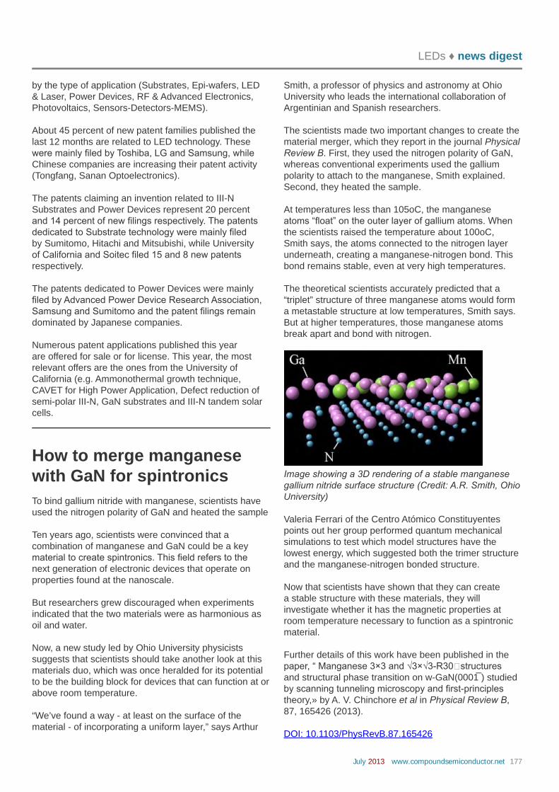
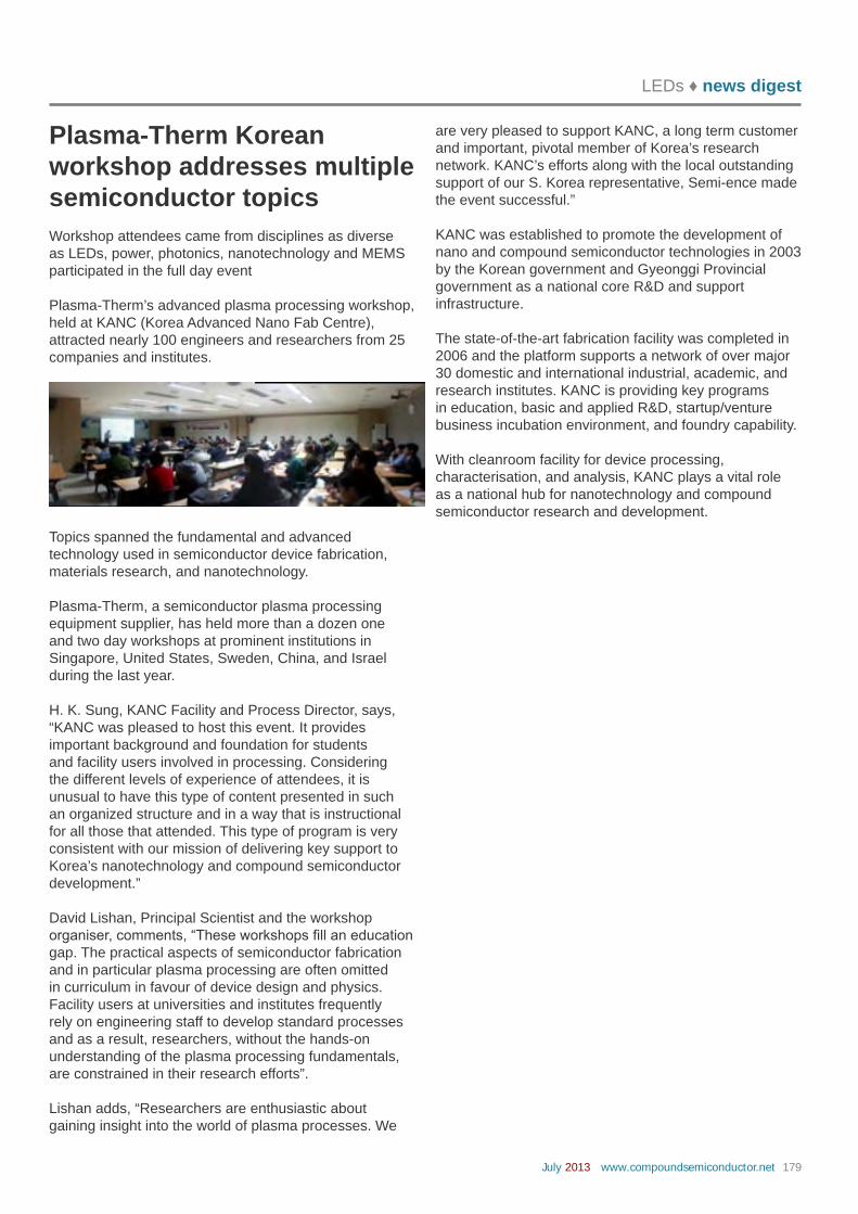
Versatile, low-cost photonic chips CPV industry’s bright future Selecting the right SiC transistor A unified theory for LED droop Maturing GaN for the US military News Review, News Analysis, Features, Research Review and much more. Free Weekly E News round up , go to www.compoundsemiconductor.net Volume 19 Issue 5 2013 @compoundsemi www.compoundsemiconductor.net Indium Scarcity claims are scaremongering
Transcript
Versatile, low-cost photonic chips
CPV industry’s bright future
Selecting the right SiC transistor
A unifi ed theory for LED droop
Maturing GaN for the US military
News Review, News Analysis, Features, Research Review and much more.
Free Weekly E News round up , go to www.compoundsemiconductor.net
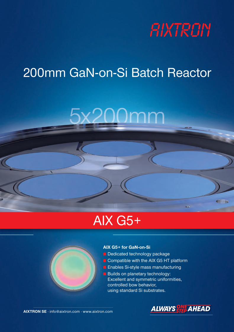
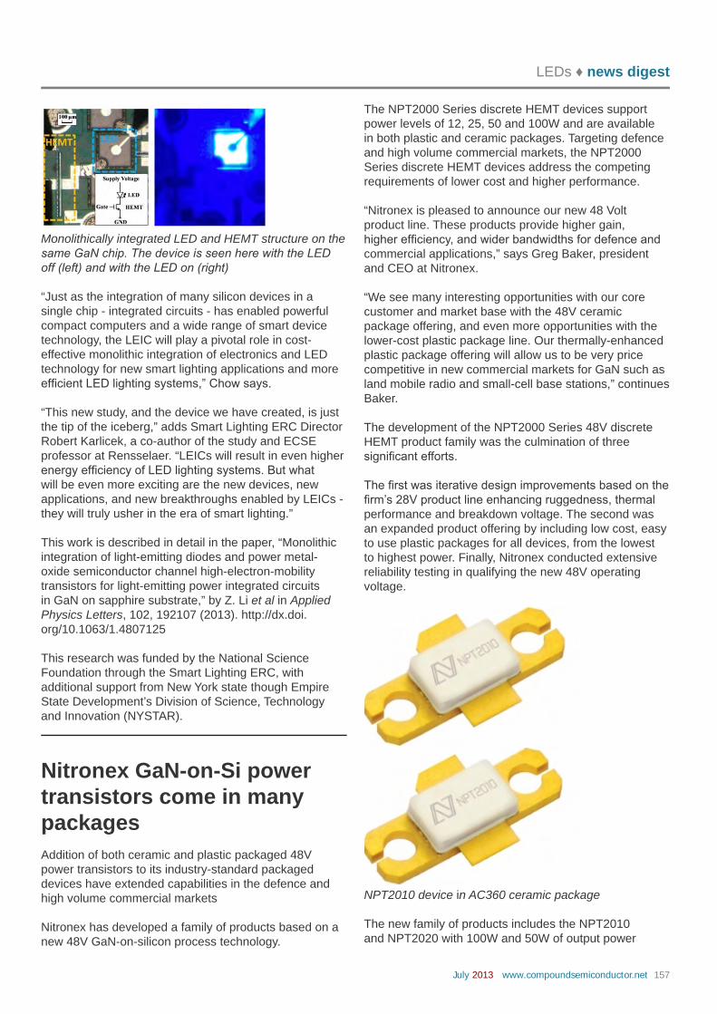
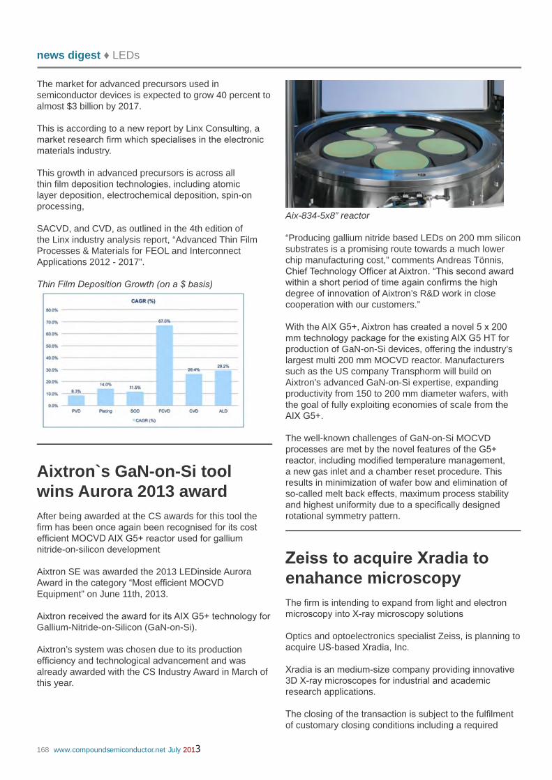
AIX G5+ for GaN-on-Si■ Dedicated technology package■ Compatible with the AIX G5 HT platform■ Enables Si-style mass manufacturing■ Builds on planetary technology: Excellent and symmetric uniformities, controlled bow behavior, using standard Si substrates.
SEVERAL THOUGHTS crossed my mind when I read of Amonix’s breaking of the record for concentrating photovoltaic (CPV) module efficiency: It was encouraging to hear of activity from a company that looked to be on the ropes; I was impressed by the raising of this bar; and lastly, I wondered how important is this success, judged against the efficiency metric.A high efficiency for a module is obviously good, and exceeding 36 percent with a 40 percent efficient cells shows just how capable Amonix’s engineers are at making the most of the sunlight incident on their optics. But the efficiency metric does not reveal how efficiently a CPV system will perform, which also depends on things like tracking accuracy and reliability.
Other factors are also important. Cost is one, which is reflected in the $/W figure that is widely used in the solar industry. But this doesn’t account for the lifetime of the system, and the time taken re-coup the investment. To assess whether the system will turn a profit or make a loss, there is the levelised-cost-of-energy: This calculates the price for generating electricity that will enable the system to break even over its lifetime.
Issues surrounding the suitability and value of metrics are not limited to CPV. High-power LED chips that are helping to usher in an era of solid-state lighting are often judged by the lumens per Watt for a given colour temperature. This figure matters, because ultra-high-efficacy chips give an LED bulb a significant
Metrics: What do they mean?
performance margin over a compact fluorescent, and ultimately a much lower running cost. But that efficacy figure doesn’t tell the whole story. There is also the price of the packaged chip, which accounts for a hefty chunk of the bulb’s bill of materials.
I could go on, weighing up the pros and cons of metrics used for other devices. But, if like most of our readers, you’re an engineer, I’m probably telling you little that you don’t know already. After all, it’s a big part of your job to not just obtain a number for a metric, but mull over its worth and come to appropriate conclusions.
Editorial View v5RS.indd 3 01/07/2013 15:13
4 www.compoundsemiconductor.net July 2013
contents
30
features
24 46
ConneCting the CoMPoUnD SeMiConDUCtor CoMMUnity Volume 19 issue 05 2013
36
Contents v1.indd 4 01/07/2013 14:51
July 2013 www.compoundsemiconductor.net 5
contents
news review: 06 Sharp’s III-V 44.4% effi cient solar cell raises the bar 07 Air Liquide acquire Voltaix 08 GaN LED shipments to top 100 billion units in 2013 10 In-Situ monitoring speeds up InP nanowire production 11 SemiLEDs expands vertical UV-LED portfolio 12 Sematech optimises device to enable III-Vs on silicon 14 Europium and magnesium co-doping creates powerful red GaN LEDs 15 Cree CXA LEDs set new benchmark
Magazine & Front Cover: Designed by Mitch Gaynor
Versatile, low-cost photonic chips
CPV industry’s bright future
Selecting the right SiC transistor
A unified theory for LED droop
Maturing GaN for the US military
News Review, News Analysis, Features, Research Review and much more.
Free Weekly E News round up , go to www.compoundsemiconductor.net
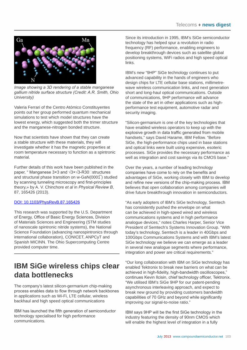
5024 Indium: Claim of scarcity is scaremongering Rumours are circulating that reserves of indium could soon run out, threatening production. But if you look at the evidence, you’ll fi nd that there is plenty of indium to go round for many decades to come.
26 CPV set for a brighter future It is diffi cult to gauge the state of the CPV industry: System manufacturers have folded and scaled back, while Soitec has announced big plans. Although life can be tough in the CPV industry, an analyst is tipping the sector to grow at a healthy rate.
30 GaN for greater military service The US Department of Defense views GaN MMICs as too expensive and insuffi ciently reliable for its needs. To address these shortcomings, it is spearheading a project to drive down cycle times, increase yield and improve reliability.
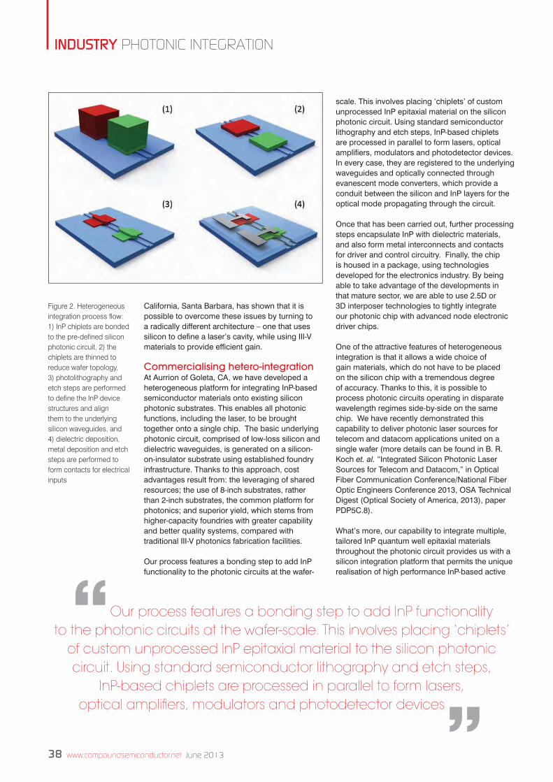
36 Uniting silicon and InP to make versatile, low-cost chips Telecom and datacom networks are under ever- increasing strain from an explosion in data transfer. What’s the long-term solution? It’s a universal photonics technology that marries InP performance with large silicon wafers.
41 Driving SiC switches Engineers can build motor drives and power supplies that deliver very high levels of effi ciency by combining frugal, fast SiC Super Junction Transistors with optimised gate drivers.
46 A unifi ed theory for LED droop What causes droop, the decline in an LED’s effi ciency as the current passing through it is cranked up? Is it Auger recombination, or could it be carrier leakage? Both camps are dismissive but maybe they shouldn’t be.
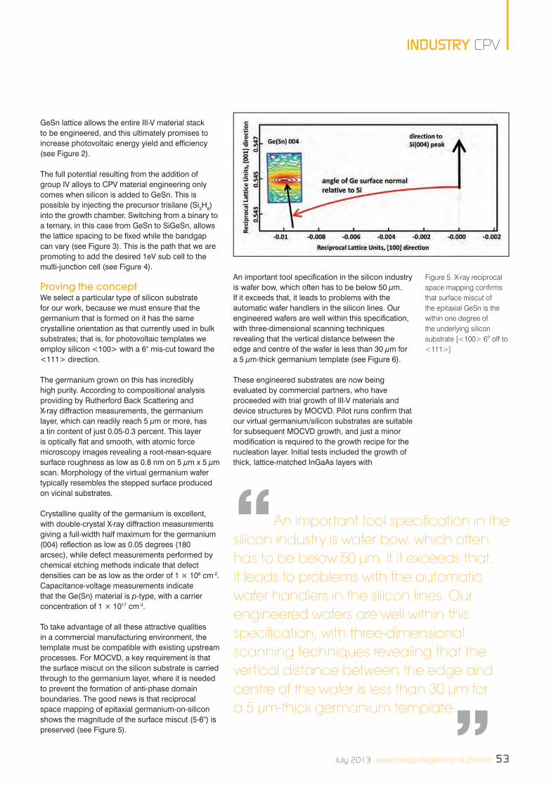
50 Germanium virtual substrates: promising for multi-junction cells Cutting cell costs will ensure that CPV become more competitive. One way to do this is to turn to silicon substrates incorporating germanium-based layers, which bridge lattice constants and allow the formation of a 1 eV junction for boosting effi ciency.
news analysis
18 Amonix: the future of concentrating PV after all?
20 CMOS poised for power amplifi er takeover
22 All change for silicon carbide
23 SiC-on-silicon edges closer to LEDs
research review
57 Semi-polar plane delivers stable green LEDs
58 Building bigger GaN ICs
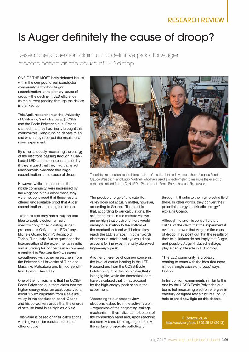
59 Is Auger defi nitely the cause of droop?
60 Flaws exposed in ZnO Hall measurements
Contents v1.indd 5 01/07/2013 14:51
6 www.compoundsemiconductor.net July 2013
NEWS REVIEW
Sharp concentrator solar cell sets new recordSharp Corporation has achieved the world’s highest solar cell conversion efficiency of 44.4%, using a concentrator triple-junction compound solar cell. these solar cells are used in a lens-based concentrator system that focuses sunlight on the cells to generate electricity.
this latest Sharp breakthrough came about through research and development efforts that are part of the “r&D on innovative Solar Cells” project promoted by Japan’s new Energy and industrial technology Development organization (nEDo). Measurement of the value—which sets a record for the world’s highest concentrating conversion efficiency—was confirmed at the Fraunhofer institute for Solar Energy Systems (iSE) in Germany.
Compound solar cells typically offer high conversion efficiency while utilizing photo-absorption layers made from compounds of multiple elements,
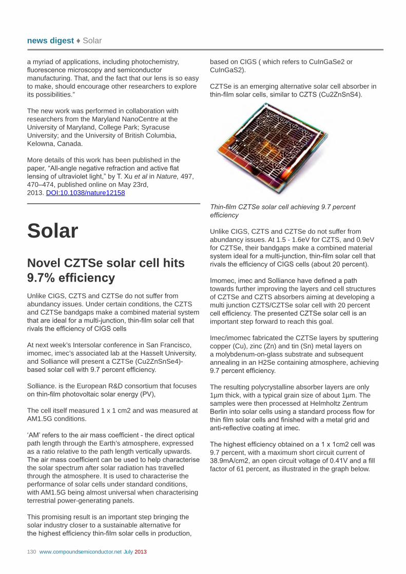
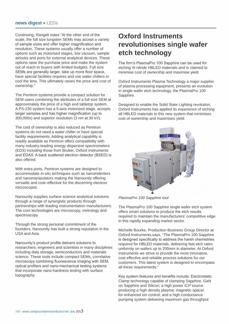
Concentrator Solar Cell with World’s Highest Conversion Efficiency of 44.4 percent
5N Plus to install gallium plant In South Korea5n pluS inC., a producer of specialty metal and chemical products, will invest in a new gallium chemicals facility to be located in South Korea, one of the fastest growing regions for electronics manufacturing in the world.the new facility should be operational before the end of 2013 and will be located within an industrial park nearby a number of important electronic manufacturing facilities. 5n plus has entered into an agreement with a local chemical distributor for the supply of operating services and logistics of the new facility.
north East asia represents the majority of the world’s lED production, and over 70 percent of the world’s electronic tablet display supply. the lED market is expected to grow at a 15-20 percent annual rate in the near to medium term, with growth mainly driven by increasing market penetration for lighting applications.
high purity gallium metal and chemicals also represent essential materials in the manufacture of products such as Gaas electronic components for 3/4G wireless applications, iGZo transparent semiconductor for next generation displays, CiGS thin film solar panels, and GaSb wafers for ir detection and imagery systems.
as a group, these applications are foreseen to drive significant growth in gallium demand in the coming years. this new investment in South Korea should serve as a platform in the future for the manufacture of other high purity materials for the asian market.
“We are pleased to be able to make this investment in gallium chemicals and demonstrate our commitment to serve our customers wherever in the world they may require our products and services,” says Jacques l’Ecuyer, president and Chief Executive officer of 5n plus. 5n plus has existing gallium chemicals manufacturing facilities in Madison, Wisconsin, uSa and in Wellingborough, uK.
such as indium and gallium. Sharp’s concentrator triple-junction compound solar cells use a proprietary technology that enables the efficient conversion of sunlight into electricity by means of a stack of three photo-absorption layers, the bottommost of which is made from inGaas (indium gallium arsenide).
to achieve a concentrating conversion efficiency of 44.4%, Sharp worked to widen the effective concentrator cell surface and ensure uniformity of width at the interface of the connecting concentrator cell and electrodes.
Because of their high conversion efficiency, compound solar cells have thus far been used primarily on space satellites.
looking to the future, Sharp aims to harness this latest development success and make the use of compound solar cells more feasible in terrestrial applications.
News CS v1.indd 6 01/07/2013 14:54
July 2013 www.compoundsemiconductor.net 7
NEWS REVIEW
Air Liquide acquires Voltaixair liquide has signed an agreement to acquire Voltaix inc., a u.S. based electronics materials company. the acquisition is expected to close later this summer, pending applicable regulatory approvals.
Founded in 1986, Voltaix is a manufacturer of materials used in the production of semiconductor devices and advanced solar cells, with expertise and global stewardship in silicon, germanium, and boron chemistries.
it operates manufacturing facilities in the u.S. in Branchburg (new Jersey), high Springs (Florida) and portland (pennsylvania) and in South Korea in Sejong-si (South Chungcheong province).
the company employs 185 employees. air liquide, with its aloha product line, is a manufacturer of advanced precursors
for semiconductor manufacturing. precursors are molecules with specific physical and chemical properties that are used for depositing critical layers during fabrication of microelectronic devices.
air liquide utilises a comprehensive process for designing, screening and industrialising advanced precursors in close cooperation with semiconductor industry leaders and process tool makers.
the acquisition of Voltaix complements the aloha offer and brings together synergies in molecule discovery and scale up, contributing to accelerate the introduction of a broader portfolio of new high-tech materials to semiconductor manufacturers and therefore enabling the increase in computing power and connectivity.
Schott And Tesat-Spacecom to soar into space
thE SChott tEChnoloGy Group and tesat-Spacecom Gmbh & Co. KG, have developed a hermetically sealed packaging solution that can be used in space. the technology is supporting the European Space agency (ESa) ’s satellite proba-V to perform Earth observations since the beginning of May. Schott says this housing contains a Gan power amplifier or MMiC chip (Monolithic Microwave integrated Circuit) for the first time ever. Schott and tesat-Spacecom optimised material composition and geometry for an optimal heat sink for this packaging. What’s more, the packaging features hermetically sealed htCC multilayer ceramics as high-frequency feed throughs that allow minimal insertion loss and reflection of the high frequency waves. the communication system for the ESa mini satellite proba-V that weighs about 140 kg is one cubic metre in size and contains a special microwave amplifier
on the basis of Gan that was installed for the first time ever there in an European Satellite. the MMiC is used to transmit photos taken at a height of roughly 800 km in the X band at 8 Ghz to monitor vegetation on our planet. the semiconductor is capable of improving signal strengths and data transmission by five to ten times and will be used as a new high-performance material in communication systems.
Monitoring of Time-Resolved Photoluminescence (TRPL) • Quality control • Materials research • Solar cell research
SemiconductorWafer Analyzer
Suited e.g. for GaAs, CdTe, CIGS, organic materialsInstrument response down to 100 ps (FWHM)Excitation and detection range:300 nm to 1700 nm
•
•
•
Applications
Features
Customized solutions
Measure minor carrier lifetimes from picosecondsto milliseconds
for individual wafers and2D lifetime imaging
News CS v1.indd 7 01/07/2013 14:54
8 www.compoundsemiconductor.net July 2013
NEWS REVIEW
GaN LED shipments to top 100 billion unitsMore than 100 billion Gan LeDs will ship in 2013. this is the equivalent of 15 for every person on the planet using this particular type of lighting device incorporating Gan. this is according to IhS’ research’s report titled “Q2 Gan LeD Supply and Demand”. With mobile phones typically containing five or 10 LeDs and televisions incorporating LeDs numbering up to the hundreds, LeD consumption is clearly accelerating. In particular, Gan LeDs account for 85 percent of total revenues
in the LeD industry, dominating key applications such as tVs and lighting. the Gan LeD market is part of the total global LeD market, including alInGaP and other LeDs, tracked by IhS on an annual basis. revenue for Gan LeDs this year will pass the $10 billion mark, notes Jamie Fox, principal analyst for Lighting and LeDs at IhS. he says, “If we consider the total LeD market - including alInGaP, Gan and other LeD types - the $10 billion revenue and the 100 billion unit shipment levels were actually reached in 2010. But now in 2013, both
of these thresholds are predicted to be attained by the Gan LeD market alone, showing how large the segment has become.”
to be sure, tremendous growth has attended the Gan LeD market in recent years. revenue in 2013 is forecast to double from that of only four years ago, while unit shipments this year will have more than tripled since 2009. even so, growth on an annual basis has been fairly uneven. In 2010, for instance, the annual revenue increase was the largest by far in the history of the LeD industry, but revenue was flat the year after. Growth then returned in 2012, climbing 15 percent. this year, revenue is forecast to be flat once again or see very little expansion, but the market can take comfort in industry total takings of $10.2 billion. another strong growth year is predicted in 2014 via general lighting along with other applications such as tVs and tablets, and then growth will slow after next year, with the double-digit revenue increases typical of years past harder to come by. Within the Gan LeD space, the market this year for Gan LeDs in lighting is projected to reach $3.4 billion, on its way to $6.7 billion by 2016. In contrast, the market for Gan LeDs in tVs will start declining as manufacturers reduce the number of LeDs utilised per television in the face of newer technology requiring fewer LeDs. From $2.1 billion this year, revenue for Gan LeDs in tVs will contract 7 percent on average every year during the next several years. a number of challenges will be in store for the LeD space moving forward. Despite the strong annual growth of recent years, overcapacity, tough competition and declining profit margins at some companies have been nipping at the industry.
News CS v1.indd 8 02/07/2013 12:59
Contact Watlow® today for the latest thermal solutions for semiconductor applications.Contact Watlow® today for the latest thermal Contact Watlow® today for the latest thermal Contact Watlow® today for the latest thermal Contact Watlow® today for the latest thermal Contact Watlow® today for the latest thermal Contact Watlow® today for the latest thermal Contact Watlow® today for the latest thermal Contact Watlow® today for the latest thermal Contact Watlow® today for the latest thermal Contact Watlow® today for the latest thermal Contact Watlow® today for the latest thermal Contact Watlow® today for the latest thermal Contact Watlow® today for the latest thermal Contact Watlow® today for the latest thermal Contact Watlow® today for the latest thermal Contact Watlow® today for the latest thermal Contact Watlow® today for the latest thermal Contact Watlow® today for the latest thermal Contact Watlow® today for the latest thermal Contact Watlow® today for the latest thermal Contact Watlow® today for the latest thermal Contact Watlow® today for the latest thermal Contact Watlow® today for the latest thermal Contact Watlow® today for the latest thermal Contact Watlow® today for the latest thermal Contact Watlow® today for the latest thermal Contact Watlow® today for the latest thermal Contact Watlow® today for the latest thermal Contact Watlow® today for the latest thermal Contact Watlow® today for the latest thermal Contact Watlow® today for the latest thermal Contact Watlow® today for the latest thermal Contact Watlow® today for the latest thermal Contact Watlow® today for the latest thermal solutions for semiconductor applications.solutions for semiconductor applications.solutions for semiconductor applications.solutions for semiconductor applications.solutions for semiconductor applications.solutions for semiconductor applications.solutions for semiconductor applications.solutions for semiconductor applications.solutions for semiconductor applications.solutions for semiconductor applications.solutions for semiconductor applications.solutions for semiconductor applications.solutions for semiconductor applications.solutions for semiconductor applications.solutions for semiconductor applications.solutions for semiconductor applications.solutions for semiconductor applications.solutions for semiconductor applications.solutions for semiconductor applications.solutions for semiconductor applications.solutions for semiconductor applications.solutions for semiconductor applications.solutions for semiconductor applications.solutions for semiconductor applications.solutions for semiconductor applications.solutions for semiconductor applications.solutions for semiconductor applications.solutions for semiconductor applications.solutions for semiconductor applications.solutions for semiconductor applications.solutions for semiconductor applications.solutions for semiconductor applications.solutions for semiconductor applications.solutions for semiconductor applications.Contact Watlow® today for the latest thermal Contact Watlow® today for the latest thermal Contact Watlow® today for the latest thermal Contact Watlow® today for the latest thermal Contact Watlow® today for the latest thermal Contact Watlow® today for the latest thermal Contact Watlow® today for the latest thermal Contact Watlow® today for the latest thermal Contact Watlow® today for the latest thermal Contact Watlow® today for the latest thermal Contact Watlow® today for the latest thermal Contact Watlow® today for the latest thermal Contact Watlow® today for the latest thermal Contact Watlow® today for the latest thermal Contact Watlow® today for the latest thermal Contact Watlow® today for the latest thermal solutions for semiconductor applications.solutions for semiconductor applications.solutions for semiconductor applications.solutions for semiconductor applications.solutions for semiconductor applications.solutions for semiconductor applications.solutions for semiconductor applications.solutions for semiconductor applications.solutions for semiconductor applications.solutions for semiconductor applications.solutions for semiconductor applications.solutions for semiconductor applications.solutions for semiconductor applications.
Optimize the Thermal Performance of your
Process Equipment.
Watlow provides innovative
solutions to help process tool
manufacturers meet the needs of the
semiconductor technology roadmap.
Our approach is to work collaboratively
to help solve complex thermal
challenges associated with state-of-the-
art manufacturing processes; helping
to improve yield, throughput and cost
of ownership. This includes innovative
heaters, controllers and sensors for use
in front-end and back-end applications
such as CVD, PECVD, Etch, Diffusion,
Bonding, IC test and more.
Extensive computational tools enable product designs to be highly refined for ultimate performance.
Multi-zone circuit layouts in a polyimide construction are highly customized to deliver exacting performance up to 250°C.
EZ-ZONE® RM Multi-loop controllers are fully scalable with up to 152 PID Loops and 256 monitor points per system.
ASSURANT™ gas and pump line heaters feature high temperature capabilities with low outgassing.
Optimize the Thermal Optimize the Thermal Optimize the Thermal Optimize the Thermal Optimize the Thermal Optimize the Thermal Optimize the Thermal Optimize the Thermal Optimize the Thermal Optimize the Thermal Optimize the Thermal Optimize the Thermal Optimize the Thermal Optimize the Thermal Optimize the Thermal Optimize the Thermal Optimize the Thermal Optimize the Thermal Optimize the Thermal Optimize the Thermal Optimize the Thermal Optimize the Thermal Optimize the Thermal Optimize the Thermal Optimize the Thermal Optimize the Thermal Optimize the Thermal Optimize the Thermal Optimize the Thermal Optimize the Thermal Optimize the Thermal Optimize the Thermal Performance of your Performance of your Performance of your Performance of your Performance of your Performance of your Performance of your Performance of your Performance of your Performance of your Performance of your Performance of your Performance of your Performance of your Performance of your Performance of your Performance of your Performance of your Performance of your Performance of your Performance of your Performance of your Performance of your Performance of your Performance of your Performance of your Performance of your Performance of your Performance of your Performance of your Performance of your Performance of your Performance of your Performance of your Performance of your Performance of your Performance of your Performance of your Performance of your
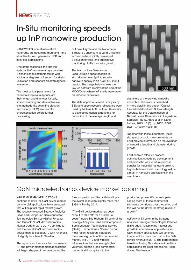
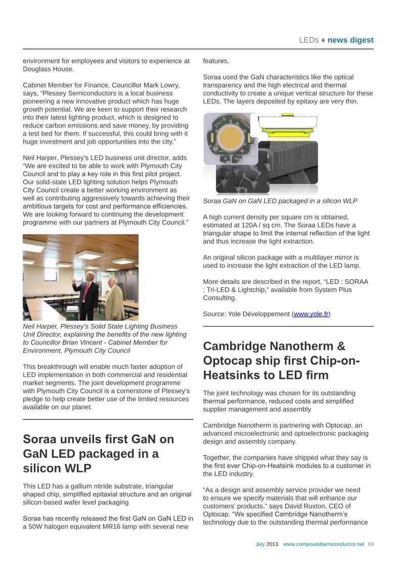
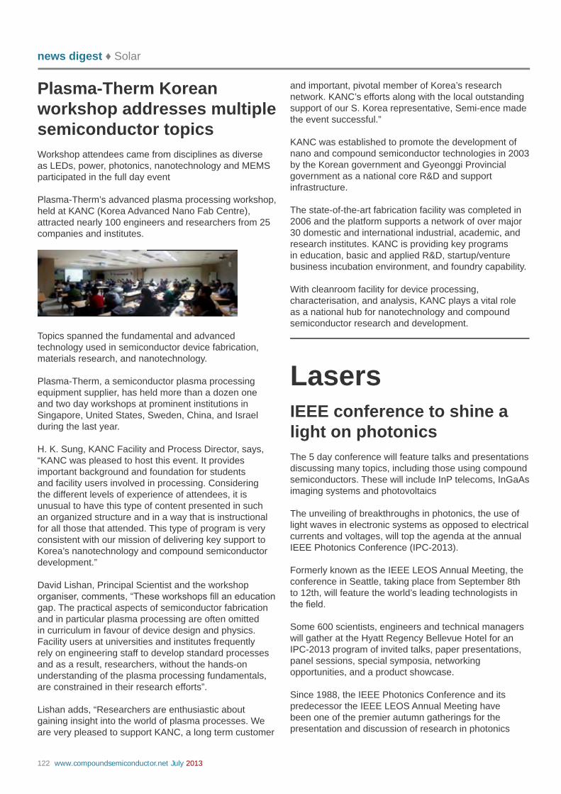
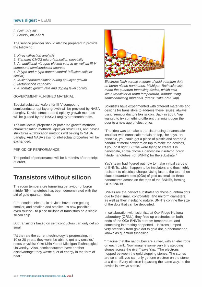
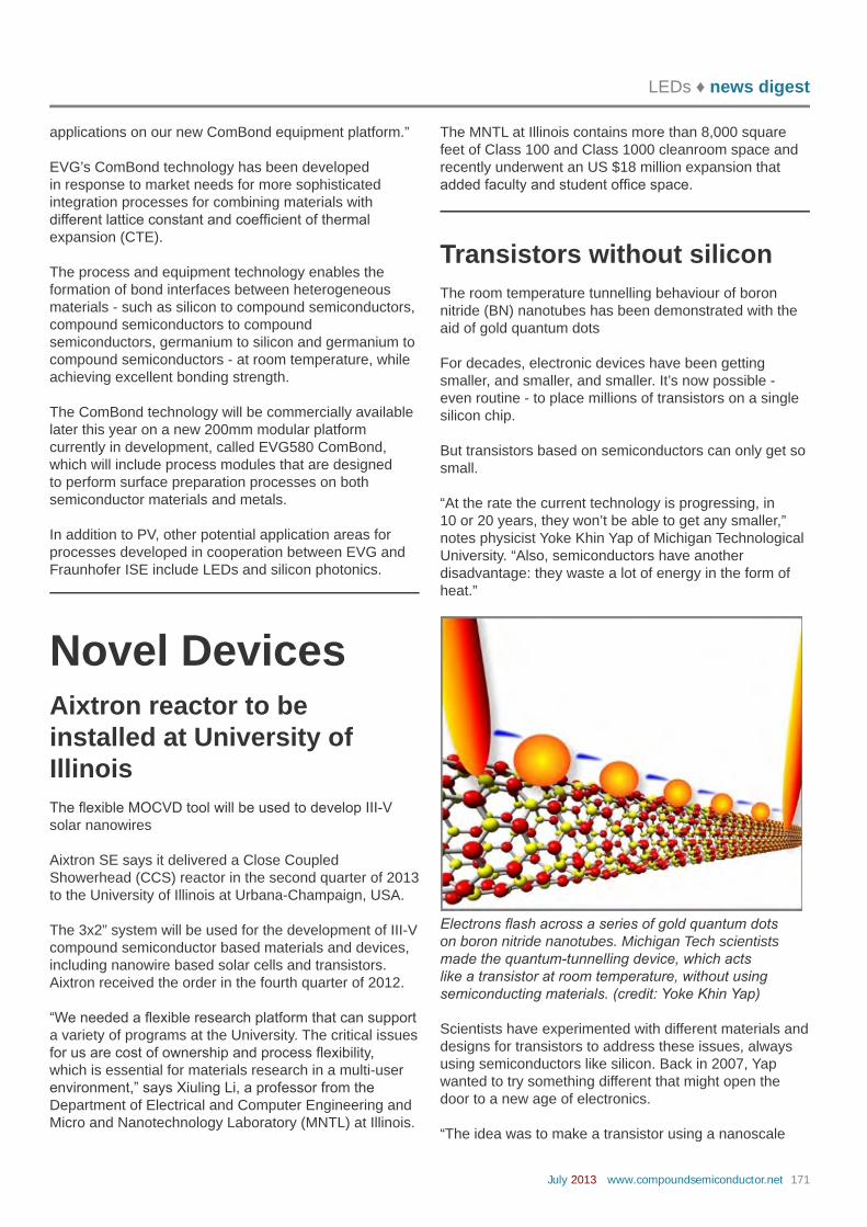
In-Situ monitoring speeds up InP nanowire productionNaNowires, sometimes called nanorods, are becoming more and more attractive for next generation LeD and solar cell applications.
one of the reasons is the fact that epitaxial iii-V nanowire arrays combine 1-dimensional electronic states with additional degrees of freedom for strain relaxation and resonant electromagnetic interaction. The most critical parameters for nanowires’ optical response are their length and diameter. Usually, time consuming and destructive ex-situ methods like scanning electron microscopy (seM) are used for characterisation before further processing.
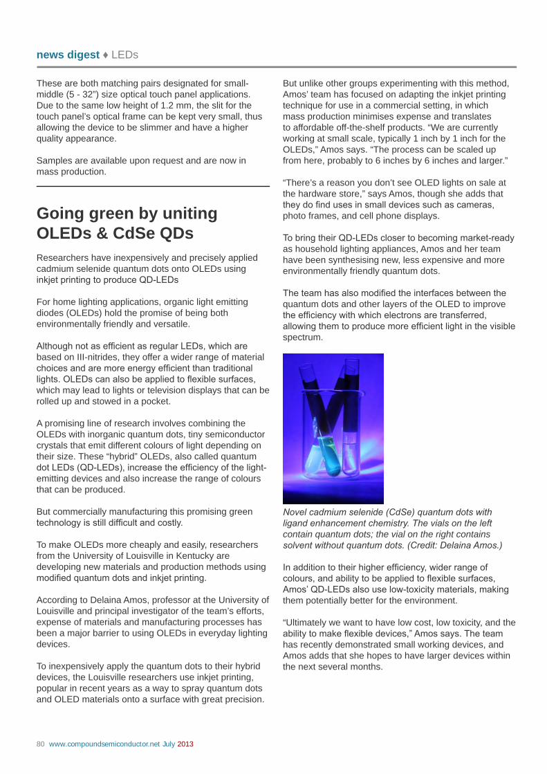
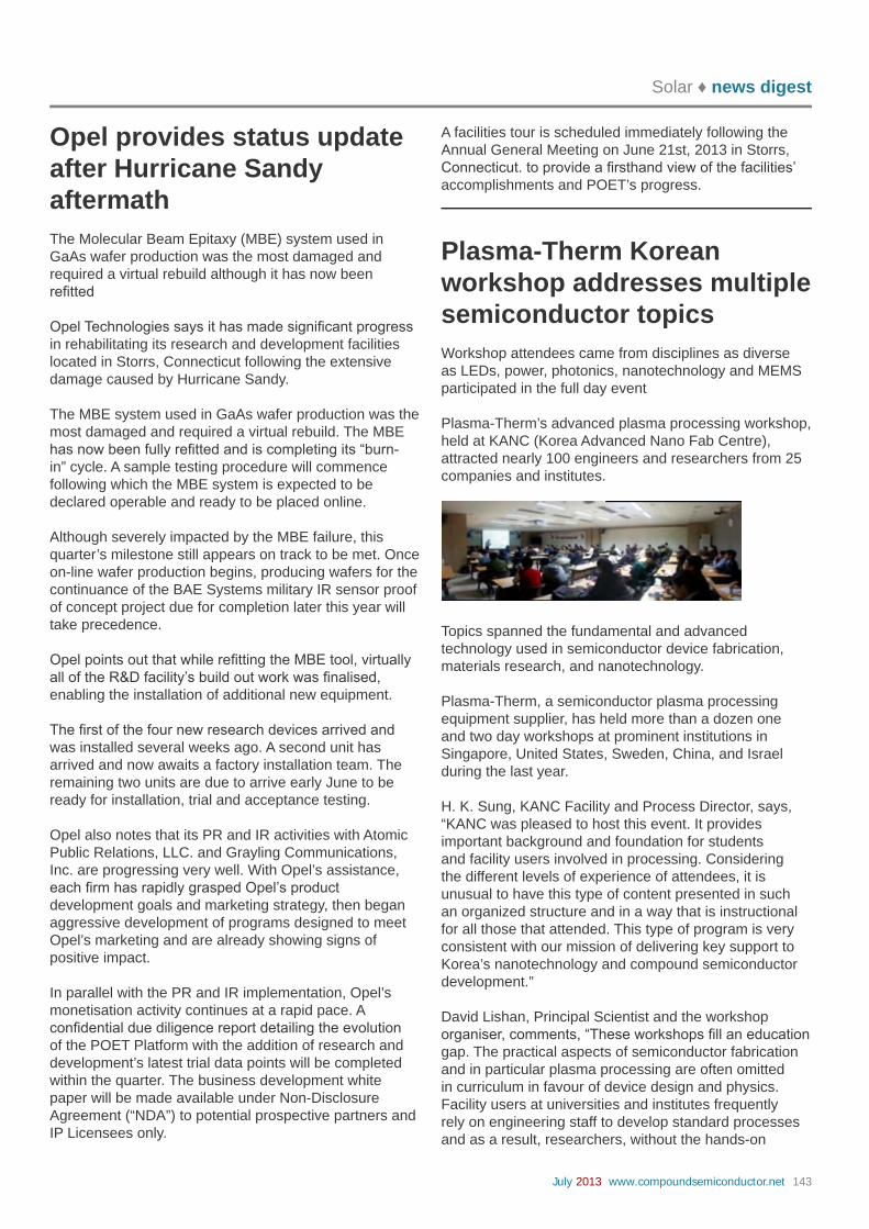
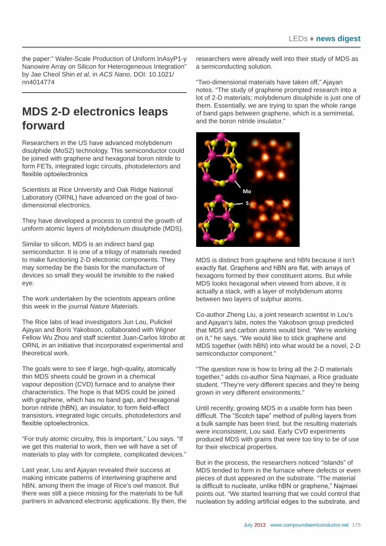
But now, LayTec and the Nanometre structure Consortium at Lund University in sweden have jointly developed a solution for real-time quantitative monitoring of iii-V nanowire growth. The team of Lars samuelson used LayTec’s spectroscopic in-situ reflectometer epir to monitor nanowire epitaxy in an aiXTroN 200/4 reactor. The image below shows the LayTec software display at the end of the MoCVD run where inP shells were grown on inP core nanowires. The data of previous ex-situ analysis by seM and spectroscopic reflectance were used by Nicklas anttu of Lund University to develop numerical algorithms for deduction of the average length and
diameters of the growing nanowire ensemble. This work is described in more detail in the paper, “optical Far-Field Method with subwavelength accuracy for the Determination of Nanostructure Dimensions in Large-area samples,” by N. anttu et al, in Nano Letters, 2013, 13 (6), pp 2662 - 2667. Doi: 10.1021/nl400811q Together with these algorithms, the in-situ spectroscopic measurements by epir provide information on the evolution of nanowire length and diameter during growth.
epir enables effective process optimisation, speeds up development and paves the way to future process transfer for industrial nanowire growth. LayTec believes in-situ metrology will be a must in nanowire applications in the near future.
GaN microelectronics device market boomingwhiLe MiLiTary aPPLiCaTioNs continue to drive the GaN device market, commercial applications have emerged that will help fuel rapid market growth. The recently released strategy analytics Gaas and Compound semiconductor Technologies service (Gaas) Forecast and outlook, “GaN Microelectronics Market Update: 2012-2017”, concludes that the overall GaN microelectronics device market closed 2012 with revenues of slightly less than $100 million. The report also forecasts that commercial rF and power management applications will begin shipping in volume during the
forecast period and this activity will push the overall market to slightly more than $334 million by 2017. “The GaN device market has been “about to take off” for a number of years,” notes eric higham, Director of the strategy analytics Gaas and Compound semiconductor Technologies service (Gaas). he continues, “Based on our most recent research, it appears there are segments of the commercial market, like CaTV and wireless infrastructure that are seeing higher volumes, but the broad commercial market is still not quite into the
production phase. we do anticipate seeing more of these commercial segments contribute over the period and this will be the driver for strong revenue growth.” asif anwar, Director in the strategy analytics strategic Technologies Practice (sTP) adds, “Despite the interest and growth in commercial applications for GaN, military applications will continue to account for more than half of the GaN device revenue in 2017. The performance benefits of using GaN devices in military applications are clear and this will keep driving GaN usage.”
News CS v1.indd 10 01/07/2013 15:05
July 2013 www.compoundsemiconductor.net 11
NEWS REVIEW
SemiLEDs expands vertical UV-LED portfolioseMiLeDs CorPoraTioN, a vertical UV-LeD technology solution provider, has released two new product families, the 10-watt high-power N9 series, and the 0.17 to 0.50-watt mid-power P50N series. Both product families take advantage of semiLeDs patented vertical LeD structure that delivers superior performance in directional industrial applications, such as printing, coating and curing, and specialty applications including signage and medical or cosmetic uses. The N9 series, housed on a 9 x 9mm ceramic package, is offered in wavelengths from 385 to 420nm in 5nm bins. Drive currents up to 1,000ma deliver a typical output of 5,000mw of optical power at the nominal 350ma drive rate at 30V.
The mid-power P50N UV-LeD series consists of a complete product family available for 0.17, 0.34 and 0.50-watt drive options, delivering up to 140mw of output, for wavelengths from 385 to 420nm in 5nm bins. The 5 x 5mm package is ideally suited for integration into compact arrays or for high-reliability backlight elements in UV-driven signage. The wide selection of output combinations simplifies the system integrator’s task by allowing a common design platform for portable
device applications, such as cosmetics or health care, where differing performance profiles are needed to address separate curing or treatment functions. “semiLeDs has consistently led the way in development of cost effective UV-LeD solutions that efficiently provide a wide range of output options, delivering the UV light where and how it is needed,” says ilkan Cokgor, semiLeDs executive VP of sales and Marketing.
The lambertian output distribution is highly compatible with secondary optics to allow precise control of the high-intensity UV light. Compared to the standard 1000 to 4000 hour life of the incumbent UV lamp technologies, vertical UV-LeD systems support lifetimes of up to 50,000 hours under optimal thermal management conditions, thereby decreasing system maintenance requirements in applications where even planned downtime carries substantial costs. what’s more, with instant on/off capabilities and a compact point-source that is compatible with a wide variety of optics, the semiLeDs N9 UV-LeD allows solution integrators to eliminate maintenance-intensive components such as mechanical shutters or focusing windows.
high-output UV sources are commonly used in semiconductor and electronic photo-resistive etching or processing, as well as high-throughput printing systems, and larger scale industrial bonding or curing applications, often eliminating the need for toxic solvents.
News CS v1.indd 11 01/07/2013 15:05
12 www.compoundsemiconductor.net July 2013
NEWS REVIEW
seMaTeCh say researchers have made significant advances in post-epitaxial growth backside clean processing that will prepare iii-V technology for high-volume manufacturing. The research was conducted at sematech’s facilities at the College of Nanoscale science and engineering (CNse) in albany, New york.
Sematech optimises device to enable III-Vs on silicon
Following a two-year effort to improve process parameters and validating iii-V on 200 mm silicon VLsi process flows, technologists identified mechanisms to enable robust backside cleaning process and made significant progress in reducing the likelihood of process cross-contamination that could impact a high-volume manufacturing line.
sematech has developed systematic experiments to identify the key mechanisms of backside contamination, which were then used to engineer robust backside clean process using standard high-volume manufacturing toolsets. at the same time, researchers assessed the environmental, safety and health (esh) risks of applying and processing compound semiconductor films on silicon dioxide wafers. “in order to drive cost-effective compliance solutions, sematech is developing new testing and analysis methodologies to evaluate esh impacts of novel materials,” says hsi-an Kwong, sematech’s esh Technology Centre program manager. “after conducting a process analysis of iii-V manufacturing line, we were able to identify potential esh risks, including generation of arsine and arsenic compounds, and develop protocols to help mitigate the impact to environment and safety.” supported by the conventional silicon CMos processing capabilities of CNse, sematech researchers are now working jointly with chipmakers, equipment and materials suppliers and universities.
They are working on the esh and contamination challenges of processing iii-V materials in a 300 mm fab in order to enable safe implementation of iii-V technology for high-volume manufacturing. iii-V compound semiconductors are considered valid candidates as building blocks for the implementation of high-performance, low-power logic devices beyond the 10 nm technology node. To be truly competitive, iii-V based technology must be monolithically integrated with silicon in order to benefit from the existing silicon-based semiconductor processing. For successful introduction into silicon manufacturing line, hetero-integrated iii-V on silicon wafers must be processed with a backside clean and capping processes. “Through the success of our research and development efforts, sematech is developing manufacturable solutions and practical implementation approaches to enable the fabrication of logic devices and systems on chips with diverse and improved functionalities,” says Paul Kirsch, director of Front end Processes (FeP) at sematech.
Meister Abrasives AG, Switzerland · www.meister-abrasives.com
Meister AbrasivesMake A Quality Decision International
News CS v1.indd 12 01/07/2013 15:05
NCC NUREMBERG, GERMANY
SIX DAYS ONE EXHIBITIONTHREE CONFERENCES
Register Online now as a delegate or visitor at www.eumweek.com
EUROPEAN MICROWAVE WEEK 2013 NÜRNBERG NCC, GERMANY,
OCTOBER 6 - 11, 2013
EUROPE’S PREMIER MICROWAVE, RF, WIRELESS AND RADAR EVENT
The Conferences:• European Microwave Integrated Circuits Conference (EuMIC) 7th – 8th October 2013
• European Microwave Conference (EuMC) 8th – 10th October 2013• European Radar Conference (EuRAD) 9th – 11th October 2013• Plus, Workshops and Short Courses (From 6th October 2013)
Delegates - Register for the conference online at www.eumweek.com
Conference fees• ADVANCE DISCOUNTED RATE – for all registrations made online until 6th September • STANDARD RATE – for all registrations made online from 7th September
For complete conference pricing, visit www.eumweek.com
The Exhibition (8th – 10th October 2013)Pivotal to the week is the European Microwave Exhibition, which offers YOU the opportunity to see, first hand, the latest technological developments from global leaders
in microwave technology, complemented by demonstrations and industrial workshops.
Visitors - Register as an Exhibition Visitor at www.eumweek.com. Entrance is FREE!
Explore transport properties of new materials that open up possibilities
for future development in fields like: semiconductors, organic electronics,
solar energy, and spintronic materials.
Untitled-1 1 01/07/2013 09:24
14 www.compoundsemiconductor.net July 2013
NEWS REVIEW
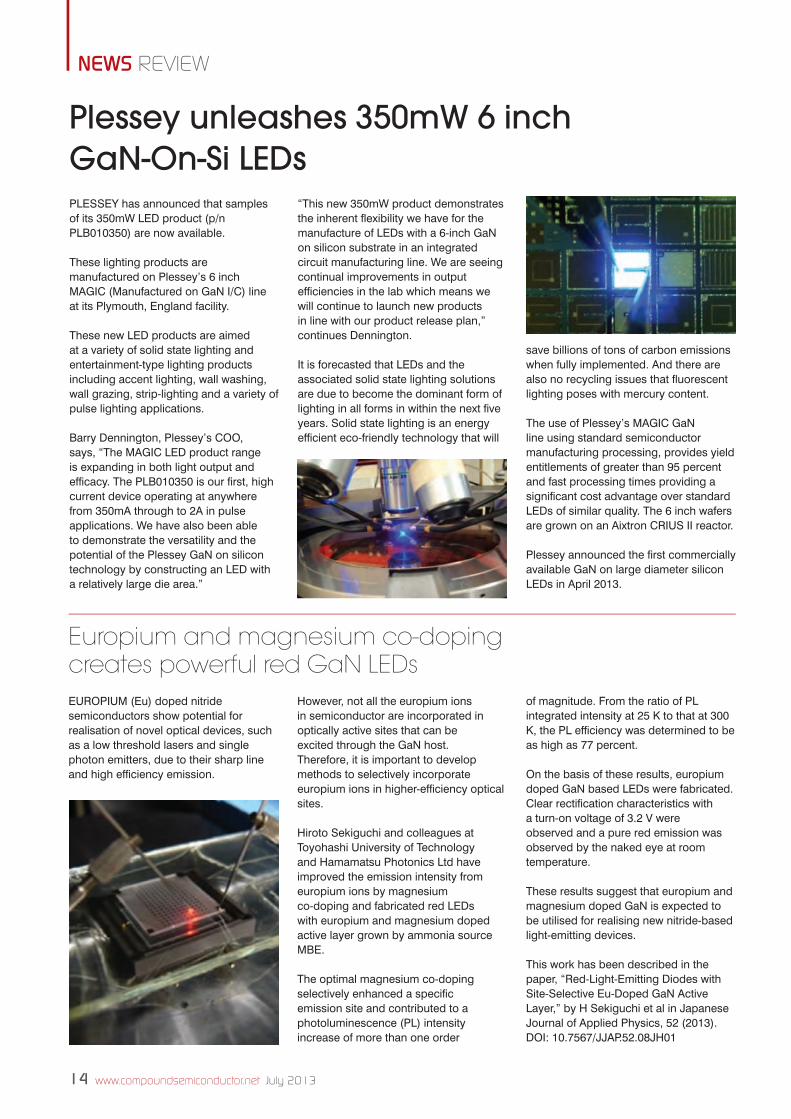
Plessey unleashes 350mW 6 inch GaN-On-Si LEDsPlessey has announced that samples of its 350mW leD product (p/n PlB010350) are now available.
These lighting products are manufactured on Plessey’s 6 inch MAGIC (Manufactured on GaN I/C) line at its Plymouth, england facility.
These new leD products are aimed at a variety of solid state lighting and entertainment-type lighting products including accent lighting, wall washing, wall grazing, strip-lighting and a variety of pulse lighting applications.
Barry Dennington, Plessey’s COO, says, “The MAGIC leD product range is expanding in both light output and efficacy. The PlB010350 is our first, high current device operating at anywhere from 350mA through to 2A in pulse applications. We have also been able to demonstrate the versatility and the potential of the Plessey GaN on silicon technology by constructing an leD with a relatively large die area.”
“This new 350mW product demonstrates the inherent flexibility we have for the manufacture of leDs with a 6-inch GaN on silicon substrate in an integrated circuit manufacturing line. We are seeing continual improvements in output efficiencies in the lab which means we will continue to launch new products in line with our product release plan,” continues Dennington.
It is forecasted that leDs and the associated solid state lighting solutions are due to become the dominant form of lighting in all forms in within the next five years. solid state lighting is an energy efficient eco-friendly technology that will
save billions of tons of carbon emissions when fully implemented. And there are also no recycling issues that fluorescent lighting poses with mercury content.
The use of Plessey’s MAGIC GaN line using standard semiconductor manufacturing processing, provides yield entitlements of greater than 95 percent and fast processing times providing a significant cost advantage over standard leDs of similar quality. The 6 inch wafers are grown on an Aixtron CRIUs II reactor.
Plessey announced the first commercially available GaN on large diameter silicon leDs in April 2013.
Europium and magnesium co-doping creates powerful red GaN LEDseUROPIUM (eu) doped nitride semiconductors show potential for realisation of novel optical devices, such as a low threshold lasers and single photon emitters, due to their sharp line and high efficiency emission.
However, not all the europium ions in semiconductor are incorporated in optically active sites that can be excited through the GaN host. Therefore, it is important to develop methods to selectively incorporate europium ions in higher-efficiency optical sites.
Hiroto sekiguchi and colleagues at Toyohashi University of Technology and Hamamatsu Photonics ltd have improved the emission intensity from europium ions by magnesium co-doping and fabricated red leDs with europium and magnesium doped active layer grown by ammonia source MBe.
The optimal magnesium co-doping selectively enhanced a specific emission site and contributed to a photoluminescence (Pl) intensity increase of more than one order
of magnitude. From the ratio of Pl integrated intensity at 25 K to that at 300 K, the Pl efficiency was determined to be as high as 77 percent.
On the basis of these results, europium doped GaN based leDs were fabricated. Clear rectification characteristics with a turn-on voltage of 3.2 V were observed and a pure red emission was observed by the naked eye at room temperature.
These results suggest that europium and magnesium doped GaN is expected to be utilised for realising new nitride-based light-emitting devices.
This work has been described in the paper, “Red-light-emitting Diodes with site-selective eu-Doped GaN Active layer,” by H sekiguchi et al in Japanese Journal of Applied Physics, 52 (2013). DOI: 10.7567/JJAP.52.08JH01
News CS v1.indd 14 02/07/2013 15:17
July 2013 www.compoundsemiconductor.net 15
NEWS REVIEW
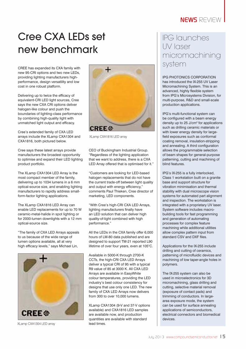
CRee has expanded its CXA family with new 95-CRI options and two new leDs, providing lighting manufacturers high-performance, design versatility and low cost in one robust platform. Delivering up to twice the efficacy of equivalent-CRI leD light sources, Cree says the new CXA CRI options deliver halogen-like colour and push the boundaries of lighting-class performance by combining high-quality light with unmatched light output and efficacy. Cree’s extended family of CXA leD arrays include the Xlamp CXA1304 and CXA1816, both pictured below. Cree says these latest arrays provide manufacturers the broadest opportunity to optimise and expand their leD lighting product portfolio. The Xlamp CXA1304 leD Array is the most compact member of the family, delivering up to 1034 lumens in a 6 mm optical-source size, and enabling lighting manufacturers to rapidly address small-form-factor lighting applications. The Xlamp CXA1816 leD Array can enable leD replacements for up to 70 W ceramic-metal-halide in spot lighting or for 2000-lumen downlights with a 12 mm optical-source size. “The family of CXA leD Arrays appeals to us because of the wide range of lumen options available, all at very high efficacy levels,” says Michael lin,
Cree CXA LEDs set new benchmark
CeO of Buckingham Industrial Group. “Regardless of the lighting application that we want to address, there is a CXA leD Array offered that is optimised for it.” “Customers are looking for leD-based halogen replacements that do not have the current trade-off between light quality and output with energy efficiency,” comments Paul Thieken, Cree director of marketing, leD components.
“With Cree’s high-CRI CXA leD Arrays, lighting manufacturers finally have an leD solution that can deliver high quality-of-light combined with high performance.” All the leDs in the CXA family offer 6,000 hours of lM-80 data published and are designed to support TM-21 reported l90 lifetime of over four years, even at 105°C. Available in 5000-K through 2700-K CCTs, the high-CRI CXA leD Arrays deliver a typical CRI of 95 with a typical R9 value of 85 at 3000 K. All CXA leD Arrays are available in easyWhite colour temperatures, providing the leD industry’s best colour consistency for designs that use only one leD. The new family of CXA leD Arrays now delivers from 300 to over 10,000 lumens. Xlamp CXA1304 (9-V and 37-V options available) and CXA1816 leD samples are available now, and production quantities are available with standard lead times. XLamp CXA1304 LED array
XLamp CXA1816 LED array
IPG launches UV laser micromachining system
IPG PHOTONICs CORPORATION has introduced the IX-255 UV laser Micromachining system. This is an advanced, highly flexible system from IPG’s Microsystems Division, for multi-purpose, R&D and small-scale production applications. IPG’s multi-functional system can be configured with a beam energy density up to 25 J/cm2 for applications such as drilling ceramic materials or with lower energy density for large-field exposures such as conformal coating removal, insulation-stripping and annealing. A third configuration allows the programmable selection of beam shapes for general-purpose patterning, cutting and machining of blind features. IPG’s IX-255 is a fully interlocked, Class 1 workstation built on a granite base and support structure for vibration minimisation and thermal stability with dual microscope vision systems for automated part alignment and inspection. The workstation is integrated with a proprietary UV laser. system software includes macro-building tools for fast programming and generation of automating processes for complex feature machining while additional utilities allow complex pattern input from standard CsV and DXF files. Applications for the IX-255 include drilling and cutting of ceramics, patterning of microfluidic devices and machining of low taper-angle holes in polymers. The IX-255 system can also be used in microelectronics for 3D micromachining, glass drilling and cutting, selective material removal (exposure of contact pads) and trimming of conductors. In large-area exposure mode, the system can be used for surface annealing applications of semiconductors, electrical connectors and biomedical devices.
News CS v1.indd 15 02/07/2013 15:17
CS International Conference 2014speakers announced!
Gain a comprehensive overview of the entire compound semiconductor industry at the leading international conference.
The 4th CS International Conference will be held at the Sheraton Frankfurt Airport Hotel, Germany, on Tuesday 18th & Wednesday 19th March 2014.
Front Ends for Mobile DevicesHandset front-ends are becoming more complex, due to an ever-increasing number of bands used for mobile communication. Will this trend play into the hands of GaAs chipmakers? Or is silicon CMOS technology going to grab market share?
Integration of CMOS and III-VsSilicon is running out of steam, and the future is widely tipped to be high-mobility channels made from germanium and III-Vs. But how will these materials be introduced in the world’s leading silicon foundries?
LEDsLEDs are the dominant source for backlighting screens of all size. So, to penetrate new markets and grow revenues, can chipmakers now trim the cost-per-lumen of the LED or equip the device with additional features?
Lasers and PICsRocketing levels of internet traffic are putting greater and greater strain on optical networks and data centres.
Can this be addressed by advancing the performance of conventional lasers, or does the market need to turn to greater use of PICs?
Power ElectronicsSilicon has dominated the power electronic market for decades, but wide bandgap semiconductors will soon replace this material. What’s the primary role for SiC, and where will GaN feature?
SolarTriple-junction solar cell efficiencies are increasing steadily. Will this help to spur rapid growth in the concentrating photovoltaic sector, or will it be more valued by those requiring a power source for satellites?
Wide Bandgap RF DevicesGaN and SiC have a great set of attributes that make them very promising materials for producing RF devices. But are they now fulfilling their potential and netting substantial sales?
This two day event covers seven themes
CS international DPS v5.indd 2 01/07/2013 15:11
Delegates will have the unique opportunity to network with the world’s top executives in compound semiconductor technology. Hear about the breakthroughs in device technology; insights into the current status and the evolution of compound semiconductor devices; and details of advances in tools and processes, which could help boost fab yields and throughputs. This event is held once a year and brings together the best in class of the compound semiconductor industry.
For maximum business benefit, book your place now and take advantage of our early bird discounted rate, available until 30th November 2013.
Please visit www.cs-international.net for further information on this event.
Company Speaker Topic Title
Keynote Speakers
Ming Su Can SiC or GaN power the next-generation hybrid electric vehicle drive systems?
Jean Fompeyrine Wafer bonding for III-V and Germanium CMOS
Mike Briere Revolutionary performance and commercialization of GaN-on-Si based power devices
Young Soo Park Slashing LED costs with 200mm silicon substrates
Presentations also from:
Gregory Fish III-V heterogeneous photonic and electronic integration on silicon
Chris Horton The promise of GaN in the RF arena
Andrew Barnes Overview of GaN reliability improvement activities at the European Space Agency
Michael Weirich Why JFETs can be a success in the power electronics market
Aaron Thean Extending Moore’s Law with III-V and Germanium
William Henry Applications and opportunities for MicroLED emitters
Jeff Sercel Insights into vertically integrated production of high-power laser systems
Pallavi Madakasira LED light bulbs: When and how will the lighting of tomorrow become the lighting of today?
Mike Mallinger New GaN series of microwave transistors, focusing on the 900MHz to 3.5 GHz bands
Petteri Uusimaa RGB laser solutions for display and projection application
Marc Rocchi 100nm GaN/Si mmW foundry service and MMICs
Valery Tolstikhin Photonic integration in InP: A regrowth-free platform for fabless manufacturing model
Ulrich Steegmueller Success factors in the increasingly competitive LED ecosystem
Vijit Sabnis Setting a new benchmark for space solar cell performance
Asif Anwar What will be the outcome of the GaAs vs silicon CMOS battle
Thomas Meier GaAs & silicon: Coexistence in a wireless world
Philippe Roussel Vertical integration vs outsourcing in the wide bandgap sector
Over 20 inspiring presentations
Connecting the leading compound semiconductor industry insiders
CS international DPS v5.indd 3 01/07/2013 15:11
18 www.compoundsemiconductor.net July 2013
NEWS ANALYSIS
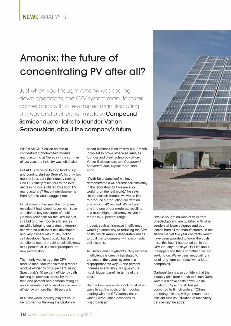
When Amonix called an end to concentrated photovoltaic module manufacturing at nevada in the summer of last year, the industry was left shaken.
But ABB’s decision to stop funding up and coming start-up GreenVolts, only two months later, sent the industry reeling. had CPV finally fallen foul to the ever-decreasing costs offered by silicon PV manufacturers? Recent developments from Amonix would suggest not.
in February of this year, the company revealed it had joined forces with Solar Junction, a key developer of multi-junction solar cells for the CPV market, in a bid to drive module efficiencies up while bringing costs down. Amonix has worked with most cell developers, and very closely with multi-junction cell developer, SpectroLab, but Solar Junction’s record-breaking cell efficiency of 44 percent at 947 suns prompted the new partnership.
Then, only weeks ago, the CPV module manufacturer claimed a record module efficiency of 36 percent, using Spectrolab’s 40 percent efficiency cells, beating its previous record by more than one percent and demonstrating an unprecedented cell to module conversion efficiency of more than 90 percent.
At a time when industry players could be forgiven for thinking the California-
Amonix: the future of concentrating PV after all?
Just when you thought Amonix was scaling down operations, the CPV system manufacturer comes back with a re-vamped manufacturing strategy and a cheaper module. Compound Semiconductor talks to founder, Vahan Garboushian, about the company’s future.
based business is on its way out, Amonix looks set to prove otherwise. And, as founder and chief technology officer, Vahan Garboushian, told Compound Semiconductor, expect more, and soon.
“[With Solar Junction] we have demonstrated a 44 percent cell efficiency in the laboratory, but we are also working on the real world,” he says. “in the next six months we would like to produce a production cell with an efficiency of 42 percent. We will put this into one of our modules, resulting in a much higher efficiency, maybe in the 37 to 38 percent range.”
indeed, such an increase in efficiency would go some way to reducing the CPV costs, which Amonix desperately needs to do if it is to compete with silicon solar cell systems.
As Garboushian highlights: “Any increase in efficiency is directly translated to the cost of the overall system in a disproportionate way. A one percent increase in efficiency will give you a much bigger benefit in terms of the cost.”
But the business is also looking at other ways to cut the costs of its modules, starting with the CPV supply chain, which Garboushian describes as “disorganised”.
“We’ve bought millions of cells from SpectroLab and are qualified with other vendors at lower volumes and buy lenses from all the manufacturers. in the silicon market five year contracts would have been awarded to lower the costs here; this hasn’t happened yet in the CPV industry,” he says. “But it’s about to happen and that’s something we are working on. We’ve been negotiating a lot of long-term contracts with a lot of companies.”
Garboushian is also confident that the industry shift from 4-inch to 6-inch GaAs wafers will drive costs down. As hepoints out, SpectroLab has just converted to 6-inch wafers. “others are doing this and will get much more efficient runs as utilisation of machinery gets better,” he adds.
News Analysis v4RS.indd 18 01/07/2013 09:30
July 2013 www.compoundsemiconductor.net 19
NEWS ANALYSIS
But crucially, the company has also made significant changes to the way it operates. With manufacturing in the US scaled back, the business is looking to the east.
“Right now we are heavily involved with opening manufacturing in the menA region and are developing joint ventures in China,” says Garboushian.
As well as these developments, the company also intends to deliver a new, cheaper version of the Amonix 7700 utility-scale CPV solar power system by the end of the year. Garboushian will not be drawn on details but says: “The new product will reduce cost substantially, we call it the 8700 system. The architecture is the same as the 7700 but we have spent the last year-and-a-half doing
everything possible to reduce cost so we can make money from it.”
“This will be introduced by the end of this year and will be in manufacturing next year,” he adds.
The current cost of an Amonix CPV module comes in at around $2.9/W while the price of other solar PV technologies is dropping below $1.9/W. however, with the new module, Garboushian is aiming for a cost of around $2/W.
“We are trying to compete with the rest of the world,” he says. “We’re establishing manufacturing, we’re looking into a very very fast ramp up. Come 2015, we will have our lowest levelised cost of electricity and several hundred mW of capacity.”
Above: The Amonix 7700 Solar Power Generator: A cheaper version is promised
for the end of this year.
Below: Vahan Garboushian, Amonix CTO,asserts that the company is looking to the Middle East and North Africa
region for manufacturing
News Analysis v4RS.indd 19 01/07/2013 09:30
20 www.compoundsemiconductor.net July 2013
NEWS ANALYSIS
in the last few weeks UK-based nujira has broken its own world record for envelope tracking (eT) linearity on a GaAs power amplifier (PA) and unveiled its highest performing eT modulator yet, primarily designed for a GaAs PA.
The double-whammy confirms that 4G smartphone volume shipments are almost upon us, but this doesn’t signal pay day for manufacturers of GaAs PAs.
“envelope tracking gives manufacturers of CmoS power amplifiers an opportunity to get a grip on the high-end smart phone market,” says Jeremy hendy, vice president of sales and marketing at nujira. “i’m not sure what percentage of power amplifiers will be CmoS in three to five years time, but my guess it will be a lot and could well be 50 percent.”
nujira has spent just over a decade developing its envelope tracking power supply technique to boost the efficiency and linearity of PAs for RF front ends. Device makers can replace the normal DC-DC converter with a power modulator that varies the supply voltage to the PA to track the amplitude of the transmitted RF signal, keeping it in compression across the entire modulation cycle, not just the peaks.
This not only boosts PA performance but enables full-power transmission from handsets, a huge bonus for LTe network operators desperate to expand the coverage area of a base station. But while envelope tracking can take GaAs PAs to linearities that CmoS alternatives can only dream of, handsets do not
CMOS poised for power amplifier takeover
As Nujira unveils its highest performing envelope tracking chip for mobile handsets yet, vice president Jeremy Hendy asserts the technology is ready for GaAs and CMOS power amplifiers.
demand this level of performance, not even 4G LTe devices. What’s more, nujira’s eT modulators now push CmoS PA performances to 4G requirements, as laboratory tests on prototype devices showed earlier this year. And according to hendy, eT technology is just as easy to use with CmoS as it is GaAs.
“There’s no real difference in how you use envelope tracking for CmoS compared to GaAs and we’ve been saying for a couple of years now that this could be key to unlock the performance of CmoS in high-end smart phones,” says hendy. “The technology levels the playing field as you are no longer reliant on the inherent linearity of the transistor.”
in response, GaAs manufacturers have continued to buy CmoS PA manufacturers. on the tail of RFmD acquiring Amalfi, Avago bought 3G CmoS PA pioneer, Javelin Semiconductor in April, while murata recently partnered with CmoS RFiC company, Peregrine Semiconductor, to develop CmoS PAs.
And as the GaAs heavyweights build up CmoS technical reserves, these businesses are still a step-ahead on optimising PA design to make the most of envelope tracking. “A lot of CmoS power amplifier companies tried to linearise the power amplifier through clever circuit design... but they went off in the wrong direction for using envelope tracking,” says hendy. “We’re now seeing the first GaAs vendors really get to grips with designing a good envelope tracking GaAs power amplifier.”
But the CmoS businesses aren’t hanging around, as evidenced by Qualcomm’s RF360, the first CmoS PA with eT, released earlier this year.
As hendy highlights, this GaAs-based multi-band, multi-mode PA alternative indicates CmoS PA manufacturers are certainly “thinking about the two in parallel”. indeed, some industry players anticipate a high-tier handset containing a Qualcomm CmoS PA to surface early next year. But will other chip-set
News Analysis v4RS.indd 20 01/07/2013 09:30
July 2013 www.compoundsemiconductor.net 21
NEWS ANALYSIS
Commercial pressures could also prompt a switch to CmoS. As hendy asserts: “Broadcom, Qualcomm, intel and nvidia; they all buy bucket loads of CmoS from TSmC.”
“These companies would much rather be in control of the supply chain that they already have, than be reliant on weird and wonderful GaAs companies such as Skyworks and RFmD to always provide them the [components] they want on time,” he adds.
So where does this leave the GaAs PA? Safe for now.
hendy asserts the lion-share of first 4G smartphones, set to ship late this year or early 2014, will come with a GaAs PA. however, he also believes CmoS with eT will “inevitably” capture market share from GaAs in the RF-front-end market.
“When you have a big player such as Qualcomm into this, everyone else will be looking into it,” he concludes.
manufacturers jump? Yes, and hendy reckons a key driver will, of course, be integration.
“Look inside some of the latest handsets with GaAs power amplifiers and you see four different GaAs dies for different bands, different modes and switches. There’s a CmoS controller, multi-chip modules... and it’s all a big mess,” he says. “With CmoS you integrate a lot of this onto the same die and get a much cleaner module.”
News Analysis v4RS.indd 21 01/07/2013 09:30
22 www.compoundsemiconductor.net July 2013
NEWS ANALYSIS
AS mAnUFACTUReRS of photovoltaic inverters and high-end power supplies embrace SiC diodes and transistors, wide bandgap device makers are braced for growth and change.
highlighting how the SiC device market bucked the power electronics downturn and grew 38 percent in 2012, Yole Developpement analyst, Philippe Roussel, forecasts continued growth, but not necessarily for the likes of Cree, infineon, microsemi and ST microelectronics.
“it’s a funny story but come 2020 the dominant country in the silicon carbide business will be Japan,” he says. “in the
coming seven years, Japan will grow from zero to [holding] the majority of the business, some 35 percent.”
Looking east, Rohm is Japan’s key SiC device manufacturer right now, but many other Japan-based businesses have also been rapidly developing related technologies. As Roussel puts it: “Japanese companies are really pushing like hell on silicon carbide development and now have plenty of really smart technology in-house. We’ve seen them really expand their businesses in the last two years and now they are moving to the next phase; commercialisation.”
indeed, the nation’s electronics conglomerates from Fuji electric and mitsubishi electric to Panasonic and Toshiba have already unveiled myriad SiC discrete diodes, transistors and power modules.
Following in the footsteps of Cree and Rohm, a key focus right now is moSFeTs with integrated diodes, but more can be expected.
“We are in touch with these companies and know they have everything they need to compete with state-of-the-art technologies,” he adds. “So now they are really pushing to launch commercial versions.”
Crucially, the majority of Japan-based electronic heavyweights have focused on the moSFeT. As Roussel puts it: “hitachi, mitsubishi, nissan, Panasonic and Toshiba... yes, they are all working on the moSFeT.” Could a plentiful source of moSFeTs finally sway industry favour towards this tried and tested transistor?
The answer is not yet obvious. And as the likes of infineon, Fairchild and United SiC continue to focus on JFeT, BJT and iGBT development, key questions remain: What markets will the new wave of wide bandgap product manufacturer
target? And will these electronics heavyweights actually deliver discrete devices or implement iCs into modules?
Looking at markets, today’s leading lights have targeted many applications. For example, Germany-based infineon has set its sights on existing smart power modules and PV inverters while US-based Cree, with its diversified product range, targets these and other markets. Japan-based players appear to be choosier.
“Rohm is really promoting silicon carbide for hybrid electric vehicles while mitsubishi is producing silicon carbide for train traction,” he says. “my feeling is if the hybrid electric vehicle market [takes off]... the Japanese will be well positioned to address it.”
But markets aside, the jury is out on whether these players will supply discretes or modules. Roussel now sees the entire SiC industry re-shaping, moving from a discrete device business to a power module business. As he points out, this was initiated by the likes of microSemi and GeneSiC delivering hybrid silicon/silicon carbide products while other players such as Rohm and mitsubishi have now unveiled full-SiC modules.
While the analyst predicts this trend will prevail in the coming years, exactly what the Japan-based players do next remains to be seen.
“Fuji for example proposes to build a silicon carbide manufacturing line with a government-founded national programme. This line will be shared between several partners and the idea is to develop devices,” he explains. “And so the question is what are these companies going to do with these devices. Will they be sold as discretes or implemented in a power module?”
As Roussel highlights, Fuji electric already manufactures power modules, Panasonic develops devices but sells systems while mitsubishi electric uses its SiC diodes and moSFeTs internally for, say, air conditioning systems.
“it really is a question of, say, will Fuji sell discrete devices? i just don’t know,” he asserts. “my feeling is Japan already has an established domestic market and so [these players] can do whatever they want.”
All change for silicon carbideWith continued growth projected for SiC markets,up and coming Japan-based manufacturers prepare to steal the show.
News Analysis v4RS.indd 22 01/07/2013 09:30
July 2013 www.compoundsemiconductor.net 23
RESEARCH REVIEW
moRe ThAn A DeCADe AGo, researchers from Australia-based Queensland micro and nanotechnology Facility (QmF) of Griffith University were depositing silicon carbide on silicon as part of a venture capital funded programme to develop novel non-volatile memory cells. Come the global financial crisis, funding waned and the project was shelved. The process, however, was not.
in 2011, the QmF researchers joined forces with micro-device equipment manufacturer, SPTS Technologies, to develop a production reactor targeted at producing SiC-coated silicon wafers for Gan for LeDs. As Alan iacopi, QmF director of operations, explains: “Silicon carbide makes a great buffer layer for Gan, but we knew that if the industry was going to take us seriously, we needed a production vehicle to commercialize the technology.”
And, today, this is what they have. Sited at QmF, the team’s vertical reactor – dubbed epiFlx – is designed for high temperature vacuum processing of large batches of wafers sized from 50 mm to 300 mm.
Right now, the team is finalising the baseline SiC-on-silicon growth processes on the reactor to produce a cost-effective buffer material. Will this at last enable LeD manufacturers to switch from sapphire to silicon substrates? iacopi and the rest of the team thinks so.
“Since march of this year we’ve been transferring our process from the original research reactor to the epiFlx and the initial uniformities are very encouraging,” says iacopi. “We’ve already achieved SiC film thickness uniformities of around 1 percent on 300 mm wafers from the epiFlx and are now characterising the processes on smaller wafers.”
At the same time, SPTS and QmF have been working with industry partners to
validate the technology within the LeD and Power Gan-on-silicon markets. Structures fabricated on silicon are already showing promising results and as SPTS chief executive, Bill Johnson, says: “These manufacturers feel that a SiC buffer layer offers a real value proposition and like the ability to have a batch tool capable of supporting multiple Gan moCVD reactors.”
Both iacopi and Johnson agree that there is no demand for 300 mm wafers right now, but as Johnson says: “We wanted to say, ‘look, here’s a 300 mm wafer with industry-leading uniformity’. it clearly shows the industry that a very uniform buffer layer can be epitaxially grown on smaller wafer sizes.”
Today, LeD manufacturers are migrating from 100 mm to 150 mm sapphire substrates to boost chip yields per wafer, but the partners are looking to enter the market with 200 mm wafers.
“The leading LeD manufacturers are now interested in 150 mm substrates and we believe that by the time we are ready with our technology, 150 mm sapphire substrates will have a usable cost structure. So 200 mm would be a logical insertion point,” says Johnson.
initial estimates suggest the team’s SiC-on-silicon coating process, in volume production, will add no more than $35 to the cost of a silicon wafer.
This, without a doubt, would draw LeD manufacturers away from large sapphire substrates, costing hundreds of dollars, but what about competition from, say, Azzurro, Translucent and Kyma? The team reckons its technology offers greater appeal than commercially-available templates.
Johnson asserts epiFlx-produced wafers would be much cheaper than templates with exotic layers produced via more expensive deposition processes while
iacopi believes his team offers a more flexible proposition.
As he highlights, many makers of buffer materials claim templates are good for LeD manufacturers to ‘play with’, but is this the case?
“LeD manufacturers can’t ‘tune’ these and will not be in control of their manufacturing process; they also can’t control how much they pay for those wafers,” he says. “With an epiFlx system, manufacturers will get a baseline process and you can imagine them tuning this for their own applications to develop a competitive advantage.”
So as the SPTS-QmF team continues to fine-tune its process, where next for the partners? “By early next year customers will be engaged in beta tests with us,” says Johnson. “This is not years away, it’s quarters away. And from a performance and cost-of-ownership point of view, epiFlx will be far and away the clear winner.”
SiC-on-silicon edges closer to LEDsWill a new buffer material for GaN tempt LED manufacturers away from sapphire and onto silicon?
The EpiFlx reactor will extend the epitaxial growth process, pioneered at QMF, to commercial scale production of SiC coated silicon wafers
News Analysis v4RS.indd 23 01/07/2013 09:30
24 www.compoundsemiconductor.net July 2013
opinion indium
Scarcity claim is scaremongeringRumours are circulating that reserves of indium could soon run out, threatening the production of displays, LEDs, and lasers. But if you take a hard look at the evidence, you’ll find that the naysayers are ill-informed and there is plenty indium to go round for many decades, argues Malcolm Harrower from Indium Corporation.
Indium v3RS.indd 24 01/07/2013 09:09
July 2013 www.compoundsemiconductor.net 25
opinion indium
Indium Corporation, motivated by our desire to ensure accuracy in the discussion surrounding the level of metal reserves, and indium in particular.
Our experts began by assessing and calculating all the known deposits of zinc, the largest source of indium. Accurate figures exist in Europe and the Americas, but only estimates are used for China and the Commonwealth of Independent States (CIS), because these regions’ figures are not easily accessible nor reliable. Summing these contributions together gives us a total of 53,000 metric tonnes (MT) of indium reserves, 30,000 MT from the West and 23,000 MT from China and the CIS. These numbers are undoubtedly significant, but how do they compare with figures for extraction and actual and predicted consumption?
The amount of indium mined from western sources is 1,000 MT a year, which equates to about one-thirtieth of the current estimate of reserves in this region. Of these reserves, one-third is not extracted, a similar proportion is left in tailings, and only about one-third is actually refined into indium metal. This leads us to estimate that for this year, production of virgin indium will total 310 MT from the West, and another 230 MT from China and the CIS, leading to an annual total of 540 MT of new material.
In addition to this virgin material, there is indium that results from the recycling of spent ITO targets. Thanks to a fast recycling time and metal turnover of three-to-four times a year, nearly 900 MT of the total 1230 MT per annum of indium used in ITO production is recovered from the production process and recycled back into metal and targets.
Other applications consume another 300 MT per year, giving a total consumption of 1550 MT per annum. Although this figure is increasing at a steady rate, so is the amount of material recovered by recycling. Given the level of reserves, it is safe to say that there is plenty of indium to go round. In fact, based on current consumption, there is enough indium to last for 100 years. So those in the compound semiconductor industry should not worry about having enough indium to make their LEDs and lasers, or whether when they go home and find that their TV has stopped working, there will be enough of this metal to make the conductive coatings on their next display.
In TODAy’S MEDIA, you’ll find plenty of stories about the gradual elimination of important natural resources and the consequences this will have on our lives when they run out. At the top of this list of resources is oil, a key fuel for transportation, heating, and the production of plastics. The concern from some quarters is that this ‘black gold’ will eventually run out, while others, who have thought about it more deeply, believe that this situation is more delicate, arguing that there are widespread, frightening consequences associated with a fall in global production.
Demand for oil is generally on the rise, and some experts predict that when it outstrips supply – a scenario that has been coined Peak Oil – the price will rocket, leading to a worldwide recession and hike in unemployment. This prediction, they say, is even backed by historical evidence. For example, following the Arab oil embargo of 1973 that cut-off global supply, the price of a barrel of oil quadrupled, leading to a doubling of US unemployment to 9 percent.
Another resource that is particularly important to our global community is indium. Indium is contained in the metal organic source trimethylindium, which is used to make blue and green LEDs. Additionally, indium is the key ingredient in indium-tin oxide (ITO), a transparent, conductive film that coats the glass used in the displays of TVs, netbooks, and smartphones. It is also a required element for IGZO transistors, which are incorporated in the latest displays that promise to take clarity to a new level by moving beyond 1080 lines. It is also featured in engine bearings and alkaline manganese batteries.
Can the arguments about Peak Oil be applied to indium? Well, not really, because there is a fundamental difference between the way that oil and indium are used. The vast majority of the oil that is produced is destroyed in a combustion process, while minerals, such as indium, can be utilised and re-utilised.
In fact, there are several sound arguments to suggest that the ‘doomsday’ oil resource scenario can be averted in indium. For starters, mines continually reinvigorate their resources through exploration and development, with technological improvements allowing extraction of reserves previously thought of as unobtainable. This means that tailings, which may be uneconomic to a particular company at one point in time, remain as reserves that can be extracted when it is economically feasible to do so. What’s more, current reserves only represent a small portion of what is available in the earth’s crust, and previously unknown deposits are being continually discovered. And there is also the large, increasingly popular option for recycling. Recycling involves more efficient use of materials in the production loop, and increasingly incorporates ‘urban mining,’ which is the recovery of resources that lie around us every day for re-use.
Recycling is a common practice in the largest single application for indium – the deposition of ITO to form a transparent electrode used in the screens of electronic devices. A vacuum process called sputtering coats this oxide to the glass, but a significant proportion of indium is left on the depleted sputtering target. This indium can be recovered using an incredibly quick process that enables an efficient use of the material in the production and process loop. This recycling ultimately contributes approximately 60 percent to the overall annual indium supply chain.
The magnitude of this supply has to be determined in order to assess the overall supply and demand for indium. In-depth calculations of this supply have been performed by our team at
A short history of indiumGERMAn ChEMISTS Ferdinand Reich and hieronymus Theodor Richter discovered indium in 1863, just in time for this element to feature in Mendeleev’s first periodic table, which came out in 1869. One of the primary reasons why it had not been discovered before then was that it had not been found in its own right as a pure, extractable metal. Instead, it was uncovered as a trace element in combination with other major metals. Indium is most commonly found in conjunction with zinc and tin deposits, and extracted along with these metals further down the refining chain after removal of the major elements. Due to this, indium is included in the pantheon of ‘minor metals.’ These minor metals have been developed as a specialty market in themselves, with companies dedicated to servicing that market, including Indium Corporation, which was founded in 1934.
Indium v3RS.indd 25 01/07/2013 09:09
26 www.compoundsemiconductor.net July 2013
INDUSTRY CPV
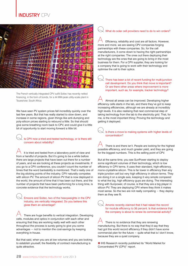
Amonix claims to have raised the record for module efficiency to 36 percent, using cells from Spectrolab
It is difficult to gauge the state of the concentrating photovoltaic (CPV) industry: Amongst system manufacturers, GreenVolts has folded and Amonix scaled back, but Soitec has announced big, bold plans. Although this indicates that life can be tough in the CPV industry, the sector should grow at a healthy rate according to research manager Sam Wilkinson from IHS, who has been talking to Richard Stevenson about the current state and prospects for this technology.
CPV looks set for a
brighter future
CPV Analyst v4RS.indd 26 01/07/2013 09:11
July 2013 www.compoundsemiconductor.net 27
INDUSTRY CPV
Q Who are the big players in the CPV industry today?
A Soitec is leading the way in terms of deployment. There
have been several announcements of the large system that it is going ahead with in Africa.
There are also a number of other companies that are still active and really pushing their technology and their product. That’s the likes of Semprius, Amonix still to a certain extent; and at the solar cell level, Emcore and Solar Junction.
Q Why have some companies in this industry, such as GreenVolts and SolFocus, folded in the last year or so?
A In any space that is largely populated by start-up
companies, it is never the case that all of the start-ups finally make it to be established companies in an established market. And the cost reductions in the silicon PV industry, which was ultimately one of the competing alternatives to CPV, made it incredibly difficult for CPV to compete in its target market. But we still believe that CPV is competitive, and can be a more attractive option in certain conditions and certain regions.
Q I presume the tough global economic conditions must have also made it hard for CPV companies to survive, let alone thrive?
A CPV companies rely heavily on financing and in today’s
climate financing is difficult to secure for any technology. Choosing where you are investing and where you are lending money − especially given all the press regarding dumping and the rate at which prices have fallen − has made investors very wary of investing in any PV technology, let alone a start-up of that kind of ilk.
Q Over the last few years, there have been several announcements of massive CPV projects, such as Soitec’s contract to supply 305 MW to San Diego County. Have these projects fallen by the wayside, or are they underway?
A The PV industry is renowned for announcements of
projects that may never happen. I remember when China first announced an incentive and there started to be a domestic market for PV in China: First Solar signed an MoU for a multi-GW plant in Inner Mongolia. That never happened, and that was probably four years ago.
The very first MoU is so far away from actually getting these projects developed and built. Some projects go ahead the whole way, and they turn into what they claimed they would be. But some never get past that very first contract because of a number of other issues, such as grid connections and financing. So many things can potentially hold up a project.
Other projects may go ahead in a much smaller version of what they claimed they were going to be. That’s probably the case with the large majority of these CPV projects. They will possibly go ahead in some format. However, I have some doubt about whether they will go ahead in the full capacity that once was claimed.
Q How many megawatts of CPV has now been installed around the globe?
A At the end of 2012, we estimated that it was around
150 MW installed in total. That’s for high and low concentration, and includes silicon CPV. The large majority of CPV is in the US.
Q In these locations, are there incentives for green technology?
A Right now in the US it’s utility driven, signing PPAs
[Power Purchase Agreements] and so on. So it’s not so much an incentive. But obviously the utilities there are required to meet certain renewables commitments, and so it is indirectly incentivised in that way.
In most other countries where CPV is deployed, it’s taking advantage of some kind of feed-in tariff, or some sort of PV incentive. There are some countries where they get an additional bonus − or there is some slightly different structure − for CPV compared to PV.
Q Can CPV make a big impact in rural locations?
A It is already being used there. We do see a huge market
for off-grid PV in general, and CPV could definitely fit into that.
Your question relates a little bit to storage. We have found that in those rural locations, the lead-acid storage battery is a huge part of that market at the moment. Over the next few years we will start to see some other new technologies, such as lithium ion and flow batteries come into that market as well. There is also a technology, sodium nickel chloride, which is from Fiam and GE. That’s got a lot of great properties for rural, off-grid use.
Q How do you expect CPV deployment to evolve in the next five years, and what factors will determine its success?
A We forecast strong growth for CPV. Obviously, it has hit a
bit of a stumbling block in the last few years with the condition of its supplier base and a number of really, really strong challengers for the suppliers that are involved, but we see it growing to reach close to 1 GW in 2016. That’s driven by strong activity in developing regions for PV: places like the Middle East, South Africa, and also a lot of activity in China.
CPV Analyst v4RS.indd 27 01/07/2013 09:11
28 www.compoundsemiconductor.net June 2013
INDUSTRY CPV
We have seen PV system prices fall incredibly quickly over the last few years. But that has really started to slow down, and increase in some regions, given things like anti-dumping and poly-silicon prices starting to rebound a little. So that should give some breathing room back to CPV, and could give it a little bit of opportunity to start moving forward a little bit.
Q Is CPV now a tried-and-tested technology, or is there still concern about reliability?
A It is tried and tested from a laboratory point of view and
from a handful of projects. But it’s going to be a while before there are large projects that have been out there for a number of years, and we are looking at these projects as investments. If you go to a CPV conference, you couldn’t count the number of times that the word bankability is mentioned. That’s really one of the big sticking points of the industry. CPV naturally competes with silicon PV. The amount of silicon PV that is now deployed in the world, the amount of time that it has been out there, and the number of projects that have been performing for a long time, is concrete evidence that the technology works.
Q Emcore and Soitec, two of the heavyweights in the CPV industry, are vertically integrated. Do you believe this gives them an advantage?
A There are huge benefits to vertical integration. Developing
cells, modules and optics in conjunction with each other and ensuring that they are working really well with each other throughout the process is surely going to give you some advantages − not to mention the cost-savings by keeping everything in-house.
But that said, when you are at low volumes and you are looking to establish yourself, the flexibility of contract manufacturing is quite attractive.
Q What do solar cell providers need to do to win orders?
A Efficiency, reliability and cost are all factors. However,
more and more, we are seeing CPV companies forging partnerships with these companies. So, for the cell manufacturers, it come down to having the right partnerships at the right companies: The ones out there deploying their technology are the ones that are going to bring in the most business for them. For a CPV supplier, they are looking for a company that is going to work with their technology and optimise the cell to their optics.
Q There has been a lot of recent funding for multi-junction cell development. Do you think that move is important? Or are there other areas where improvement is more important, such as, for example, tracker technology?
A Almost all areas can be improved. Developing higher
efficiency cells starts in the lab, and there they’ve got to keep increasing efficiencies, although we are already at incredibly high levels. It is also realising that next commercial step of taking technology from the lab to the electricity grid. That, for me, is the most important thing: Proving the technology and getting it deployed.
Q Is there a move to making systems with higher levels of concentration?
A There is and there isn’t. People are looking for the highest
possible efficiency, and much greater yield, and they are going for the biggest numbers. This is the selling point of CPV.
But at the same time, you see SunPower starting to deploy some significant volumes of their technology, which is low efficiency in CPV terms. It uses their standard, high-efficiency, mono-crystalline silicon. This is far lower in efficiency than any triple-junction cell but very high efficiency in silicon terms. They are doing it on a single axis, keeping it very simple compared to what the big, high efficiency guys are doing. The interesting thing with Sunpower, of course, is that they are a big player in silicon PV. They are deploying CPV where they think it makes most sense. So the two are not really competing − they deploy them as they see fit.
Q Amonix recently claimed that it had raised the record for module efficiency to 36 percent. Is that evidence that the company is about to renew its commercial activity?
A There is no evidence that they are renewing
manufacturing. But there is no way that they’d say that they had got this world record efficiency if they didn’t have some commercial plan for the future − quite what that is I don’t know, because they are a quiet company.
£ IHS Research recently published its “World Market for Concentrated PV (CPV)” report.
The French vertically integrated CPV outfit Soitec has recently netted financing, in the form of bonds, for a 44 MW-peak utility-scale plant in Touwsrivier, South Africa
CPV Analyst v4RS.indd 28 01/07/2013 09:11
“Now offering Germanium Reclaim”
New CS APP ready for Download NOW!
Wafer-bonding for telco VCSELs
GaN HEMTsDitching the package
Extending the life of fab tools
GaAs will fend off the CMOS threat
UCSB: Auger causes LED droop
Scrutinizing GaN HEMT interfaces
News Review, News Analysis, Features, Research Review and much more.
Free Weekly E News round up , go to www.compoundsemiconductor.net
News Review, News Analysis, Features, Research Review and much more.
Free Weekly E News round up , go to www.compoundsemiconductor.net
Volume 19 Issue 4 2013 @compoundsemi
www.compoundsemiconductor.net
Compound Semiconductor is pleased to announce the NEW APP for iPhone, iPad, iPod and android, continuing our aim of connecting the compound semiconductor industry.
Available FREE from the App Store or Google Play, the app keeps you up to date with:
Latest industry news Latest features Latest magazine articles and more...
GaN has Great characteristics for making rF transistors. this material can be used to build devices that are head-and-shoulders above those which are made from Gaas: they deliver far higher efficiencies, produce far higher power densities and bandwidths, and are able to operate at much higher temperatures.
this wonderful set of attributes has not escaped the notice of the Us military, which views this wide bandgap transistor as a very promising component for many aspects of electronic warfare, including electronic attack, electronic protection and electronic warfare support. For example, GaN rF chips could be used in the construction of phased array antennas, which will be deployed in radar and electronic systems.
to aid the development of GaN rF devices for military applications, the Defense advanced research Projects agency (DarPa) has funded the development of this wide bandgap technology through initiatives such as the Wide Bandgap semiconductor for rF applications program. efforts such as this are focused on technology development, and they are typically high-risk, high pay-off investments. in the case of GaN, they have borne much fruit, so the government services – the Navy, air Force and army – are now keen to also help to take the maturity of GaN rF technology to a new level.
Preparing GaN for
greater military serviceThe US Department of Defense views GaN MMICs as too expensive and insufficiently reliable for its needs. To address these shortcomings, it is spearheading a project to drive down cycle times, increase yield and improve reliability. Richard Stevenson reports.
to do this, the Department of Defense (DoD) is funding a title iii program for GaN rF technology. the official goal for the latest effort – which follows title iii programs on silicon-on-sapphire, Gaas wafers, inP, and sic wafers and MMics – is to instantiate a production capability defined as a manufacturing readiness level of 8: this means that the process is ready for low rate initial production in a DoD acquisition programme.
“[the project] is considered a success if the production processes are capable of producing devices of sufficient yield, cost, performance and reliability to be advantageous to both defence and commercial customers,” explains the programme’s manager, Gene himes. he knows that the production capacity/capability enabled by the title iii program should be self-sustaining long after the project is over. to try and put this into place, the project will address the high cost of GaN devices and their reliability, and involve measures to increase the yield, throughput and capacity of GaN lines in Us companies.
The big four three of the biggest Us chipmakers that already have GaN production capability are currently involved in the title iii program, while a fourth is just starting out. raytheon is running an X-band (7-11.2 Ghz) project that started in 2010; cree and triQuint are engaged in independent programmes for s-band
Title III v3RS.indd 30 01/07/2013 15:07
July 2013 www.compoundsemiconductor.net 31
INDUSTRY GaN
(2-4 Ghz) and wideband (6-18 Ghz) MMics that kicked off in 2011 and 2010, respectively; and there is also a Ku-band (7-11 Ghz) MMic project by Northrop Grumman that starts this year.
insights into the progress of the first three of these programmes were offered at the cs Mantech conference held in New Orleans from 13 May to 16 May 2013.
at this meeting, cree Program Manager ryan Fury detailed improvements to the company’s 75 W s-band and 25 W wideband die, which are fabricated with the company’s G28V3 and G28V4 heMt processes, respectively. cree introduced the latter process in 2007 to target a variety of DoD and commercial applications.
“the first volume applications were for jammers,” says Fury, who explains that cree’s GaN devices were used in products sent to iraq and afghanistan to prevent radio-controlled detonation of improvised explosive devices (ieDs). “Over 300,000 high performance, multi-stage GaN MMic power amplifiers were sold using our G28V3 process,” reveals Fury, who adds that more recently the process has been used to make products for military radar, cable tV and telecom infrastructure.
cree has recently introduced a higher voltage variant of the G28V3 process, the G50V3 – it is designed for 50 V operation. “this process provides almost twice the power density of our baseline 28 Volt process, and is ideally suited for high power radar and low cost telecom infrastructure applications, where either high power or low cost – in terms of dollars-per-Watt of rF output power – are critically important.”
in 2012, the Durham-headquartered chipmaker expanded its GaN portfolio even further, adding a G28V4 process to plug the gap between 6 Ghz and 18 Ghz that was not addressed by the 0.4 μm G28V3 processes. this higher-frequency process can be used to make products for X-band radar, electronic warfare jammers and satellite communication systems.
“We’ve also introduced a higher-voltage version of the X/Ku-band process, the G40V4, which operates at 40 volts,” says Fury. “ this is ideally suited for high frequency, pulsed-power applications, such as travelling-wave tube replacements.”
the major difference between the V3 and V4 processes is the gate length: it is 0.4 μm in the former process, but in the latter it is just 0.25 μm. standard optical lithography and a single siN etch is used to realise the 0.4 μm gate length, while the shorter variant is fabricated with optical lithography and a standard
Title III v3RS.indd 31 01/07/2013 15:07
32 www.compoundsemiconductor.net July 2013
INDUSTRY GaN
sidewall spacer. source-connected field plates are employed to increase gain and rF power density. Using a second field-plate also trims peak fields within the transistor, so this device can last longer. thanks to the use of optimised field plates, the 1 ma/mm breakdown voltage of these heMts exceeds 120 V.
at the beginning of the title iii program, cree’s engineers carried out a baseline assessment of the production cost, yield, cycle time and performance of their s-band and eW-band MMics, which were formed by depositing an insulating GaN buffer and alN and alGaN cap layers on 100 mm semi-insulating sic substrates by MOcVD. this initial study showed that cree’s process exceeded the baseline key performance parameters set out by the title iii program, with yields up to 75 percent above the benchmark, and cycle times 42 percent quicker than the initial standard.
During the programme, efforts have focused on driving yield higher, trimming cycle times and reducing manufacturing costs. this has included work to optimise gate metal electrode lift-off and reduce the number of damage sites; a switch to a new post-backside de-bond process that cuts front-side damage and drives down cycle time; and the qualification of a siN passivation tool from a manually loaded, older PecVD platform to an automated version that diminishes particle count and reduces handling damage.
these efforts have increased yield, while cutting cycle time and cost. s-band and eW-band yields are 8 percent and 18 percent above the mid-point goals for the programme, while the MMic cost and cycle time are 36 percent and 25 percent below the interim benchmark (see Figure 1).
cost savings have been realised, thanks to cutting material costs, increasing automation and boosting throughput. “higher factory loading is primarily due to the rapid adoption of our GaN products for high-volume markets, such as telecom base stations,” explains Fury. “these cost savings are helping us to further increase GaN penetration into the military and commercial markets.”
high reliability is another target within the title iii program. For continuous operation at a temperature of 125 °c for the back of the MMic die – which equates to a maximum junction temperature of 225 °c – the mean-time-to-failure (MttF) goal is a million hours. cree’s MMics are far more reliable than that, with MttF values of 55 million hours for the G28V3 process and 150 million hours for the G28V4 process. “Our GaN process has the highest rated operational channel temperature of any currently on the market,” claims Fury.
it might seem that with goals appearing to be met so easily, these targets should have been higher. But that misses the point. “the goals were structured to ensure that cree would be able to produce GaN products with the cost, performance and reliability needed to support a number of critical Us defence programmes,” says Fury.
One key challenge remains for cree in this title iii program: Passing an 8000-hour, rF high-temperature operating life test. this is designed to provide an additional assessment of the robustness of the process.
cree is now involved in the final assessment phase of the programme. however, its processes have been independently assessed by two different external customers. they have judged
The Title III program will help to reduce the cost and increase the reliability of GaN MMICs that can be used for X-band radar systems. Examples of this type of system include the sea-based X-band radar, which can provide highly advanced ballistic missile detection to discriminate a hostile warhead from decoys and countermeasures. Credit: US Navy
Title III v3RS.indd 32 01/07/2013 15:07
July 2013 www.compoundsemiconductor.net 33
INDUSTRY GaN
that it is has reached a manufacturing readiness level of 8. in addition, the company is using the lessons it has learnt form the programme as it is developing of a high frequency, Ka-band (26.5 Ghz to 40 Ghz) process, known as V5. “this will employ a 0.15 μm gate length using the same robust optical lithography process that has been improved on this programme,” says Fury.
TriQuint’s approachLike cree, triQuint semiconductor has long history in the development and manufacturing of GaN MMics. its efforts in this area date back to 1999, and nearly a decade later, in 2008, it released a qualified manufacturing process for GaN MMics on 3-inch sic substrates. two years after this, the company released a 4-inch process, which is used for standard product development and foundry projects for external customers.
efforts in the title iii program have revolved around two devices that have been designed for high power and power-added efficiency: an s-band MMic, which is a two-stage power amplifier; and a wideband Pa that covers the X-band and the Ku-bands. Both amplifiers are fabricated from heMts formed on 100 mm, c-plane 6h and 4h semi-insulating sic wafers featuring nitride epilayers deposited by MOcVD. electron-beam patterning defines the 0.25 μm gate length, with devices sporting a source-connected field plate to reduce high-field-related device degradation.
During the improve-and-refine phase of the programme, triQuint’s engineers have focused on tightening manufacturing process variability; implementing GaN-specific characterisation and tracking, as well as cutting cycle time.
“the refinements we have undertaken are based on well-developed, design-of-experiment techniques, since multiple material and process interactions can occur,” explains Douglas reep, senior Director of research in the infrastructure and Defense Products division at triQuint. “resolving issues isn’t always easy, but when statistical techniques are employed, good manufacturing solutions are what we expect.”
this approach uncovered a source of a wafer-to-wafer dependence associated with the nitride capacitor deposition process. this variation stemmed from a coupling of the wafer to the plasma deposition system, and it was eliminated by adjusting one of the process steps.
another area where triQuint has improved is tightening variations in gate leakage, which can be impacted by the condition of the surface. engineers looked at the impact of changes to process and tool, and have moved to equipment with automation, which improves process monitoring, and implemented a new process that reduces defects.
resist removal procedures were also scrutinized at triQuint. improvements in physical cleanliness led to a substantial fall in defects, but these refinements at individual steps in the process failed to tighten variations in electrical characteristics. however, when the new processes were used throughout the GaN flow, they drove a significant reduction in variability.
One possible cause for variation in devices is differences in substrate quality. traditional optical inspection is not particularly
useful, because it cannot detect scratches, due to the transparency of sic. to address this, and also provide a means of categorising defects such as micropipes, scratches and particles, triQuint has invested in a candela inspection tool. the engineers are in the process of establishing correlation between device failures and incoming material defects.
cycle times have been reduced during the title iii program. throughput of a sic/GaN via etch step has been aided by the qualification of a second etch tool, and cycle times have been slashed by a factor of three by increasing the via etch rate. this involved optimising power and pressure, and also led to improved uniformity. switching from e-beam to optical lithography could lead to further reductions in cycle time. “We have several processes that employ only optical lithography, and we use e-beam where we are pushing for performance growth and flexibility. For example, several of the new products we announced at iMs are manufactured using our latest tQGaN15 technology, which uses e-beam lithography to define its 0.15 μm gates,” explains reep.
reliability has also been assessed in triQuint’s title iii program. the MttF is greater than 10 million hours at a channel temperature of 200 °c, and in excess of 1 million hours at 225 °c. Like cree, results on the 8,000-hour operational life are still to be reported.
Cree has supplied the US army with over 300,000 multi-stage GaN MMICs, which have been used to build systems that can jam signals for setting-off improvised explosive devices. Credit: US Army
Title III v3RS.indd 33 01/07/2013 15:07
34 www.compoundsemiconductor.net July 2013
INDUSTRY GaN
Raytheon’s refinementsraytheon’s engineers started work on their title iii program back in 2009, and have now realised the primary goal, demonstrating and validating manufacturing readiness level 8 and qualifying this process for insertion into DoD production systems.
this project involved three major tasks: processing 24 wafers with the baseline production process to evaluate yield and reliability; reducing variations through identification of root causes, using a minimum of 150 wafers; and processing 24 wafers with the improved process, to demonstrate that the requirements for manufacturing readiness level 8 have been satisfied.
For the first part of this project, 24 wafers were processed with a mask set that included Fets, small MMics for reliability evaluation and large periphery X-band MMics for yield evaluation. reasonable yields were obtained for the latter device, but they were less than those for comparably sized Gaas MMics. Meanwhile, reliability assessments based on three-temperature, Dc arhenius testing fulfilled the programme
objective for MttF, but a small proportion of the devices under test exhibited early degradation at 380 °c. this initial study shaped the primary goals for the next phase of the project: to improve X-band MMic yield to a level comparable to that for Gaas MMics, and to eliminate early degradation observed in a small proportion of devices at elevated temperatures.
success resulted from increasing the yield of capacitors and improving the gate process, which largely addressed the early degradation issue. engineers also investigated more aggressive Dc and rF screening tests. More stringent screening reduced yield at the wafer level, but was beneficial elsewhere, leading to dramatic improvements in the predictability of reliability data and next-level assembly yield.
an assessment of the rF operating life of the devices was made at this point in the project, with the performance of seven X-band MMics scrutinised during a 5,000-hour test, where they were driven in continuous-wave operation. No discernable change in power could be seen during this evaluation.
By the end of the project, GaN process yield more than tripled to a level that is comparable with raytheon’s Gaas process. this gain contributed to a fall of greater than 75 percent in the cost-per-Watt associated with GaN, making it three times cheaper than Gaas, according to calculations that include substrate costs.
reliability assessments at the end of the project show a MttF at 150 °c of greater than a billion hours, more than three orders of magnitude higher than the goal set out in the programme. even the time to 1 percent failure is more than 10 million hours.
himes is pleased with the progress made by raytheon, and also that accomplished by cree and triQuint: “each of our GaN projects has demonstrated tremendous success in establishing mature and capable production processes.” he attributes this success to outstanding industry-government partnerships involving talented, committed industry teams that communicate bi-weekly with their government partners.
Figure 1: Through process improvements, such as refinements to the gate metal lift-off procedure and the post-backside de-bond process, Cree’s engineers have reduced the cycle time of their manufacturing process and increased its yield
There are 10 manufacturing readiness levels associated with the Title III program
Title III v3RS.indd 34 01/07/2013 15:07
SEMICON
SEMICON
SEMICON
SEMICON
SEMICON
SEMICON
SEMICONThe largest and most influential microelectronics industry event in Taiwan
brings the world’s leading manufacturers together with 600 exhibitors and
over 1,200 booths display. Attend SEMICON Taiwan to learn the newest
technology trends and extend your industry network!
Theme Pavilions● 3D IC & Substrates● Precision Machinery
● No Waiting Line at Site ● Free Limited Edition Souvenirs● Daily Lucky Draw● Forum Early Bird Price
Search for “SEMICON Taiwan” on APP Store or Google Play!
Organizer Co-organizer
● Green Manufacturing● Secondary Equipment
● MEMS
Country Pavilions
International Forums
Co-located Events
Register before August 9th and get These Bonuses
Don’t Miss a Thing!
● Cross-strait ● USA
● Korea● Moscow
● Kyushu
Sept. 4 – 6, 2013TWTC Nangang
Exhibition Hill
Wed.Sept.4
Thru.Sept.5
Fri.Sept.6
AM PM
● Market Trends Forum● IMEC Technology Forum
● Advanced Packaging Technology Symposium● LED Forum● Green Manufacturing Forum
● MEMS Forum● IC Design Forum
● CMP Forum● MEMORY System Executive Forum
● Litho/Mask Technology SymposiumSE
MICON
SEMICON
● Executive Summit
● LED Workshop
● 450mm Supply Chain Forum
Register Now ! www.semicontaiwan.org
Untitled-2 1 28/06/2013 11:17
INDUSTRY PHOTONIC INTEGRATION
36 www.compoundsemiconductor.net July 2013
Uniting silicon and InP to make versatile, low-cost photonic chipsTelecom and datacom networks are under ever-increasing strain from an explosion in data transfer. What’s the long-term solution? It’s a universal photonics technology that marries InP performance with large silicon wafers, argue Daniel Sparacin and Greg Fish from Aurrion.
Aurion v6RS.indd 36 01/07/2013 09:13
July 2013 www.compoundsemiconductor.net 37
INDUSTRY PHOTONIC INTEGRATION
It takes just a year and a half for the bandwidth demand for telecommunications networks to double. the primary drivers for this are the soaring number of networked devices – half of americans now have smart phones – and an increase in data downloaded from the likes of Netflix, amazon and itunes.
rocketing levels of data transfer don’t just strain the telecom networks – they also create an unprecedented challenge for their datacom siblings. Lying at the heart of these datacom networks are datacenters, which are used for a diverse range of applications and can often feature tens of thousands of servers. these servers require flexible, agile interconnect networks, which must be capable of allocating jobs to any server, at any time, to respond to user demand.
the telecom and datacom networks, which work together to control the flow of internet traffic, place different demands on the evolution of the underlying interconnect technology. Long-haul telecom technology is optimised for spectral efficiency and high bandwidth, due to the cost of deploying fibers in the field. In comparison, short-reach datacom technology offers a cost-effective, low-power approach for connecting extremely large numbers of data ports in a single location. these differences account for the need for: high-performance components in telecom networks; and for lower-cost components, which can be made in far higher volumes, in datacom networks.
Scaling issuesProducts for serving both of these networks must deliver increases in performance as their dimensions are reduced. this performance-scaling requirement suggests that the only viable route ahead is a chip-based approach, rather than conventional discrete component assembly. this should cater for increases in the bandwidth requirements per transceiver, along with its complexity and component count.
It is tough to scale existing photonic technologies for datacom networks, because next-generation products have to be cheaper, produced in higher volumes, run off less power, and be housed in smaller packages. On the long-haul side of the industry, the focus has been on developing high-performance transceivers based on complex, InP-based photonic integrated circuits (PICs). these chips have satisfied performance requirements, but if they are to meet the cost and volume needs of datacentre interconnects, a significant ramp in manufacturing capability must occur. today, the incumbent technology in that sector is a combination of VCseLs and
Figure 1. Relative bandwidth growth for different sectors normalized to the year 2010. Source: IEEE 802.3 BWA Ad Hoc Report, 19th July 2012
multi-mode fiber. this product serves low-cost, high-volume markets by delivering high aggregate bandwidths, but it lacks sufficient reach for large datacentres.
In contrast, silicon photonics – a relatively new area of the photonics industry – promises to provide a platform that will scale to fulfill the demands of next-generation datacom interconnects. Its attractive features include: the ability to digitally enhance photonics through co-design of optical devices in silicon with electronics; the leveraging of high-precision, shared foundries using wafers with diameters of up to 12-inches; and silicon’s compatibility with the developments in advanced packaging. the latter attribute means that there is potential to move photonics out of a ‘gold box’ package and into one with intimate interconnection to the electronic chip.
Despite all its potential, commercial realization of silicon photonics is taking longer than many had hoped for. up until now, the laser has been segregated from the rest of the chip, leading to compromised system architecture: the laser is then treated like a power supply and split into many parallel channels, leading to a hike in cabling costs, rather than utilising the spectrally allocated bandwidth provided by wavelength division multiplexing (WDM) systems.
One upshot of separating the laser from the rest of the chip is that it delays penetration of silicon photonics into datacom markets. Performance is also compromised, preventing this technology from impacting most telecom markets. However, early work in heterogeneous integration by groups at Intel, Ghent university and the university of
Aurion v6RS.indd 37 01/07/2013 09:13
38 www.compoundsemiconductor.net June 2013
INDUSTRY PHOTONIC INTEGRATION
California, santa Barbara, has shown that it is possible to overcome these issues by turning to a radically different architecture – one that uses silicon to define a laser’s cavity, while using III-V materials to provide efficient gain.
Commercialising hetero-integrationat aurrion of Goleta, Ca, we have developed a heterogeneous platform for integrating InP-based semiconductor materials onto existing silicon photonic substrates. this enables all photonic functions, including the laser, to be brought together onto a single chip. the basic underlying photonic circuit, comprised of low-loss silicon and dielectric waveguides, is generated on a silicon-on-insulator substrate using established foundry infrastructure. thanks to this approach, cost advantages result from: the leveraging of shared resources; the use of 8-inch substrates, rather than 2-inch substrates, the common platform for photonics; and superior yield, which stems from higher-capacity foundries with greater capability and better quality systems, compared with traditional III-V photonics fabrication facilities.
Our process features a bonding step to add InP functionality to the photonic circuits at the wafer-
scale. this involves placing ‘chiplets’ of custom unprocessed InP epitaxial material on the silicon photonic circuit. using standard semiconductor lithography and etch steps, InP-based chiplets are processed in parallel to form lasers, optical amplifiers, modulators and photodetector devices. In every case, they are registered to the underlying waveguides and optically connected through evanescent mode converters, which provide a conduit between the silicon and InP layers for the optical mode propagating through the circuit.
Once that has been carried out, further processing steps encapsulate InP with dielectric materials, and also form metal interconnects and contacts for driver and control circuitry. Finally, the chip is housed in a package, using technologies developed for the electronics industry. By being able to take advantage of the developments in that mature sector, we are able to use 2.5D or 3D interposer technologies to tightly integrate our photonic chip with advanced node electronic driver chips.
One of the attractive features of heterogeneous integration is that it allows a wide choice of gain materials, which do not have to be placed on the silicon chip with a tremendous degree of accuracy. thanks to this, it is possible to process photonic circuits operating in disparate wavelength regimes side-by-side on the same chip. We have recently demonstrated this capability to deliver photonic laser sources for telecom and datacom applications united on a single wafer (more details can be found in B. r. koch et. al. “Integrated silicon Photonic Laser sources for telecom and Datacom,” in Optical Fiber Communication Conference/National Fiber Optic engineers Conference 2013, Osa technical Digest (Optical society of america, 2013), paper PDP5C.8).
What’s more, our capability to integrate multiple, tailored InP quantum well epitaxial materials throughout the photonic circuit provides us with a silicon integration platform that permits the unique realisation of high performance InP-based active
Figure 2. Heterogeneous integration process flow: 1) InP chiplets are bonded to the pre-defined silicon photonic circuit, 2) the chiplets are thinned to reduce wafer topology, 3) photolithography and etch steps are performed to define the InP device structures and align them to the underlying silicon waveguides, and 4) dielectric deposition, metal deposition and etch steps are performed to form contacts for electrical inputs
“Our process features a bonding step to add InP functionality to the photonic circuits at the wafer-scale. This involves placing ‘chiplets’
of custom unprocessed InP epitaxial material to the silicon photonic circuit. Using standard semiconductor lithography and etch steps,
InP-based chiplets are processed in parallel to form lasers,optical amplifiers, modulators and photodetector devices
”Aurion v6RS.indd 38 01/07/2013 09:13
July 2013 www.compoundsemiconductor.net 39
INDUSTRY PHOTONIC INTEGRATION
devices and silicon-based passive devices on a single chip. this means that in addition to an InP-based laser, we can build circuits featuring InP-based modulator and detector devices, which deliver superior electro-optic performance compared with traditional silicon photonic p-i-n modulators and germanium detectors.
arguably, by far the biggest benefi t of our heterogeneous integration platform is that it enables a manufacturing capability that can process a variety of PICs simultaneously. this can usher in a new era, assigning the one-product/one-process cost-structure to the history books. Lower-volume photonic components operating at unique wavelengths, such as telecom or military focused PICs, can then be produced on the same lines used to make higher-volume components, such as datacom interconnects or fi ber-access network transceivers. this will break the strong tie between volume and cost, leading to new application areas and wider usage of photonic components.
Promising prototypesOur photonic technology is directly applicable to several near-term datacom and telecom transmitter needs, including an uncooled 16-channel fi xed wavelength datacom laser array that we have produced (see Figure 4). this array not only provides a path for a less expensive version of current 100G standards,
such as the Ieee 100GBase-Lr4, which only requires 4 laser wavelengths – it also addresses the recently announced 400 Gbit/s ethernet standard that could be defi ned for 16 laser wavelengths. By further integrating this existing laser array with modulators, photodetectors, wavelength multiplexors and demultiplexors – library components which already exist in the silicon photonic toolbox – it is possible to realize a chip-scale, multi-channel WDM silicon photonic transmitter that can fi nally address existing and future standards.
similarly, our telecom wavelength laser, which produces in excess of 20 mW and can be tuned over more than 45 nm, can be readily integrated on a single chip with coherent modulators and polarization diversity optics to meet OIF 100G standards for metro telecom applications.
In both the examples just described, the unique attributes of our heterogeneous integration platform enable a complex, highly functional single-chip product that can be manufactured at a relatively low cost. such a chip can scale with the requirements of current and future generations of datacom and telecom interconnect technologies, providing the bandwidth, density and cost needed over the coming decades.
Figure 4. 16-channel fi xed-wavelength laser array fabricated on silicon and suitable for datacom transmitters
Figure 3. Aurrion’s unique heterogeneous integration process enables coherent 100G telecom transmitters and 16 channel 400 Gbit/s datacom transmitters to be fabricated simultaneously on the same silicon wafer using existing foundry infrastructure
Aurion v6RS.indd 39 01/07/2013 09:13
PCS PIRANHAPre-Pump PlasmaPFC Abatement
CLEANSORB®
Pump ExhaustDry Bed Scrubber
CLEANVENTGas Supply Purge Gas Scrubber
CLEAN-PROTECTEmergency GasRelease Scrubber
Exhaust Gas AbatementSafe and eco-friendly solutions where you need them
5 Safe, dry chemical conversion of toxic gases to stable solids
5 Proprietary CLEANSORB® media
5 No handling of toxic waste
5 Practically maintenance-free
5 Local refill service worldwide
3 Over 25 years of experience
3 More than 5000 installations worldwide
Find out more:
www.cscleansystems.com
cs clean systems anzeige 12 12 12 20.12.12 09:50 Seite 1
Manufacturer of Molybdenum.Components for MBE.Specialized Cleaning & Degassing available.
RABOUTET S.A.250 Av Louis Armand Z.I Des Grand PrésF-74300 Cluses FranceTél : 33 (0)4 50 98 15 18 Fax : 33 (0)4 50 98 92 57E-mail : [email protected] http://www.raboutet.fr
RABOUTET S.A.
VALVED CRACKER SOURCE FOR PHOSPHORUS : KPC SERIES
I N N O V A T I V E S O L U T I O N S F O R S E M I C O N D U C T O R I N D U S T R Y
Fast and precise control over phosphorus flux
100% leak tight all metal metering valve
Wide product range from 250 cc to 2500 cc
Low condenser temperature to avoid Pwhite instabilities
“Zero burst” patented design
Three-zone temperature concept
Full modularity of the design for simple P charge loading, maintenance or further upgrading
Contact [email protected] for more information 31 Rue Casimir Perier 95873 BEZONS – FRANCE Tel : + 33(0) 1 39 96 65 00 Fax : +33(0) 1 39 47 45 62www.riber.com
Untitled-1 1 01/07/2013 09:28
July 2013 www.compoundsemiconductor.net 41
Industry: SiC power electronics
Today the silicon IGBT reigns supreme in motor drives and industrial automation systems, where it is used to process voltage and current waveforms and deliver optimum power for dC-dC conversion and aC-dC/dC-aC power conversion. But this device is under increasing threat from transistors built from SiC and GaN.
Both of these alternatives have several similar, attractive characteristics. For example, they have breakdown electric fields that are around an order of magnitude higher than that for silicon – these unlock the door to new device designs, which are much thinner than the incumbent and feature blocking layers with higher doping levels. other strengths of these wide bandgap transistors, which stem from bandgaps that are around three times that of silicon, include the ability to operate at much higher temperatures and stand up to high-radiation environments. What’s more, in the case of SiC, the thermal conductivity of this material is much higher than that for silicon, so dissipated heat can be more readily extracted from the device. This, in turn, allows more power to be applied to the device before it exceeds a certain temperature.
GaN versus SiCToday, GaN power switches continue their relentless progress by increasing their blocking voltage capabilities, but are still limited to ratings less than 400 V in commercial offerings. The switches offered to date are normally-on (depletion mode) devices that require a negative gate bias to turn them off. Circuit designers find this a significant hindrance, so some switch makers deploy a low voltage silicon MoSFET in a Cascode configuration with the normally-on GaN FET to achieve a normally-off operation. Such a circuit element can be driven using standard silicon MoSFET drivers, but may suffer from parasitic inductances associated with such a connection.
Driving SiC switches
Engineers can build motor drives and power supplies that deliver very high levels of efficiency by combining frugal, fast SiC Super Junction Transistors with optimised gate drivers, argues Ranbir Singh from GeneSiC Semiconductor.
When it comes to SiC, many companies are developing and producing different types of transistors, with their own advantages and disadvantages. at GeneSiC of dulles, Va, we are pioneering SiC Super Junction Transistors (SJTs), which are gate-oxide free, normally-off, majority carrier devices. They are competing for sales with the likes of power MoSFETs (including planar dMoSFETs and trench-MoSFETs) and (normally-on and normally-off) JFETs.
Vast differences in the intrinsic material properties between SiC and silicon mean that although a particular device stole the show with the incumbent material, it is not necessarily destined to be the outright leader in the SiC arena. Instead, an alternative device may be more promising, because when it is made from SiC, it may exploit the best material properties of SiC, and minimise the use of properties where SiC lags behind silicon.
Two of GeneSiC’s SiC devices: a 1200 V/ 6A SJT chip and a 10 kV/10 A SJT chip
GeneSiC v5RS.indd 41 01/07/2013 09:10
42 www.compoundsemiconductor.net July 2013
Industry: SiC power electronics
For example, the silicon BJT (and the IGBT) exhibit minority carriers in the drain region, which are not present in the SiC equivalent. This allows the wide bandgap device to operate at very high frequencies, like a majority carrier device, so it is not plagued by dynamic breakdown issues, such as a poor reverse-bias safe-operating-area (RBSoa). Meanwhile, contemporary SiC MoSFETs have channel mobilities that are just 5-10 percent of that of silicon MoS devices, and the high doping levels found in the drain regions of normally-off SiC JFETs have made it very challenging to manufacture this device with high yields and uniform characteristics. The SJT, in comparison, is hallmarked by: a very high current gain, which can be in excess of 100 and allows low gate currents; and a good RBSoa profile, which is indicative of the robustness of this device.
Driver considerationsThese comparisons of device performance have limited worthiness, because any critical assessment of the suitability of the device for industrial deployment must not be restricted to simply its standalone performance, or even the combination of this and its cost. Instead, meaningful judgement of the merit of any class of transistor must include an analysis of how easily it can fit in with existing drive infrastructure.
dominance of the silicon IGBT in many motor controls and power supplies has led to widespread use of voltage-controlled drivers in these applications. Modern gate drivers generally switch at +15 V levels and feature higher current sourcing/sinking capabilities than their predecessors. Current levels are now several amperes, to accommodate high operating frequencies and large gate capacitances, in both IGBTs and high-current MoSFETs.
one of the downsides of the contemporary SiC MoSFET is that it requires a higher drive voltage than that produced by many, but not all, modern gate drivers: It needs +20 V to achieve a sufficiently low on-resistance. This higher-voltage requirement results from poor transconductance, which can be traced back to the low channel mobilities of SiC. Far lower drive voltages are possible with some classes of SiC transistor that involve a junction-based approach. Junction transistors and normally-off JFETs require just a +4 V drive, but may require non-zero continuous gate currents; while normally-on JFETs may need a negative bias of up to 30 V to turn them off.
This brief overview of voltage requirements for many different classes of SiC transistor appears to imply that all devices require a non-standard gate driver. Given that, it is not surprising that many SiC device manufacturers are actively working on optimum gate drivers for their switch offerings. However, it is possible to use off-the-shelf IGBT
Figure 1: Several different SiC switch technologies have been developed. In addition to the junction transistor, a form of which is made by GeneSiC, there are planar MOSFETs, trench MOSFETs and JFETs
Figure 2: The SJT produced by GeneSiC, which can be driven by a gate drive IC, must be capable of supplying a continuous current of 0.5 A to the gate of this transistor. The external parallel gate resistor, RGP, should be adjusted to meet this requirement, while the external parallel capacitor, CGP, can be chosen to ensure an optimum level of dynamic gate current during turn-on and turn-off initial transients. This dynamic current is essential for fast charging of the internal gate-source capacitance. The presence of this paralleled resistor and capacitor on the output of the gate driver can increase the device switching speed, reduce its switching loss and also cut driver losses
Figure 3: Turn-on (top) and turn-off (bottom) switching waveforms of a 1200 V / 6 A SJT (GA06JT12-247)
GeneSiC v5RS.indd 42 01/07/2013 09:10
July 2013 www.compoundsemiconductor.net 43
Industry: SiC power electronics
drivers with our SiC SJTs because their continuous gate current requirement can be supplied by such ICs. The magnitude of this current can be controlled with a series gate resistance, similar to that used in an IGBT drive, and its addition can also provide the requisite gate-source voltage (3-4 V) for operating this class of junction transistor.
one option for driving all these switches is to combine a commercial gate driver IC with an isolated input signal and a resistor-capacitor output network (see Figure 2). Using this approach, our SJTs can be driven with gate voltages as low as 8–10 V. one additional benefit of using this particular type of SiC switch is that it does not require a negative gate voltage to remain off.
due to the high voltages being switched, the input signal source from potential high drain voltages needs to be protected with an optocoupler or isolator. The isolation rating of this component should greatly exceed the predicted dC voltages in use, particularly with an inductive load present. Choke coils can also be inserted if common-mode noise in the circuit on voltage supplies and gate driver inputs and outputs is too high.
Dynamic considerationsThese gate drive considerations only take into account steady state, on-state operation, and it is much more important to consider dynamic losses at high operating frequencies. This is because SiC switches lead to the biggest gains in efficiency over the silicon incumbents when they operate at tens or hundreds of kilohertz. operating in this regime, the losses associated with the driver and the entire system are dominated by charging and discharging of the gate-source and the Miller capacitances (the capacitances seen looking into the input).
driver switching losses are directly proportional to the product of the gate-source (CGS) capacitance and the square of the voltage swing. This swing is typically 4-5 V for SJTs and normally-off JFETs, but it can be as high as 20-30 V for MoSFETs
and normally-on JFETs – implying that dynamic capacitive losses in the latter devices can be up to 50 times higher. Meanwhile, the device switching loss is governed by the gate-drain (CGd, Miller) capacitance and the square of the device voltage swing, which could be as high as 800 V. Today, the value of CGd can be two-to-three times lower for SJTs and normally-off JFETs, compared with a MoSFET of a similar current rating. So, in summary, SJTs and normally-off JFETs are significantly ahead of their SiC rivals, when it comes to efficient operation in driver circuits.
We have assessed the switching performance of our SJT in the gate drive circuit outlined in Figure 2 using an industry standard, double-pulse switching test. Measurements reveal a current rise time, tr, of only 16 ns, and a fall time, tf, of 26 ns (voltage and current waveforms of the SJT are shown in Figure 3). Total device switching energy loss is only 97 µJ per cycle, equating to less than 10 W of device switching loss at 100 kHz, while switching 600 V/6 a (3.6 kW).
Lower losses are possible by turning to a parallel resistor and capacitor on the gate driver IC output, similar to that used in high frequency IGBT drivers. With this change, a dynamic gate current waveform is introduced – due to the presence of a transient gate current peak from the charging of the gate capacitor – and this turns the SJT on and off more quickly (see Figure 5 for an example).
It is possible to alter the static and dynamic performance of the SJT – and to ultimately trade-off the switching speed to the device and the driver losses to fit the particular application demands – by adjusting the gate resistor, capacitor, and gate driver output voltage. For a fixed driver output voltage, higher capacitance leads to higher current peaks (see Figure 6(a)) with shorter rise and fall times (see Figure 6 (b)). However, increasing capacitance can have its downsides, such as higher device and driver losses (see Figures 6 (c)). So it is important to hit a sweet spot, where the gate capacitance is low enough to trim device and driver losses but still high enough to obtain desired switching speeds. Care must also be taken to avoid ringing, which may occur in the gate drive output network due to interplay between the gate capacitance and the
Figure 4: An industry standard, double-pulse switching test demonstrates GeneSiC’s SJT switching performance using the gate drive circuit detailed in Figure 2. During testing, the SJT is turned on with the application of a gate current IG and the drain current ID is ramped up linearly while flowing through the inductor and SJT in series until ID hits 6 A. At that point the SJT is switched off, and then switched back on after a 2 µs delay to record device turn-on
Figure 5: The waveform of the transient gate current, IG, while driving a 1200 V / 6 A SJT. Similar gate current switching transients are observed in MOSFET and IGBTs as well
In industrial applications, higher efficiencies are being reached through greater deployment of fast, power-semiconductor switches in variable speed drive motors
GeneSiC v5RS.indd 43 01/07/2013 09:10
44 www.compoundsemiconductor.net July 2013
Industry: SiC power electronics
parasitic inductances in the gate drive circuit. one good remedy is to place a low-inductance resistor in series with the gate capacitance.
another variable is the gate driver output voltage, which impacts SJT performance. This voltage must be high enough to bias the SJT gate-source junction on – it has a built-in voltage of about 2.8 V – and supply the steady state gate current that follows the gate current peak. There are no trade-offs associated with increasing the voltage, which leads to a nearly linear decrease in total energy and rise and fall times (see Figure 7). However, using an excessively high gate driver output voltage is not to be recommended, because this can be a large contributor to gate driver loss and steady state driver losses. a superior solution, called a 2-level driver, is provided by Rabkowski et. al. (see further reading). This uses two current levels to drive SJTs – one during the transients, and another during the steady state operation of these devices.
When we drive our 1200 V/6 a SJT with a judicious choice of gate driver output voltage and gate capacitance and resistance values, we obtain very low power losses. Using a duty cycle of 0.7 and a frequency of 500 kHz, the steady state loss for the driver is 3.85 W, while the switching losses for the driver and SJT are 0.54 W and 45.6 W, respectively. These switching losses are frequency dependent, and dominate below 70 kHz (see Figure 8).
The discussion provided here illustrates that replacing silicon IGBTs with SiC switches may not always give engineers of power circuits the ease of use that they may have anticipated, due to the drive requirements of particular classes of this wide bandgap device. However, our measurements show that one type of device, our SJT, can work very well with a conventional gate drive. Its strengths include fast switching speeds and ultra-low losses, and it is not plagued with many of the drawbacks of other SiC transistors and bipolar silicon devices.
Further readingd. Veereddy et. al. Bodo´s Power Systems, pp. 36–38 oct-2011.S. Sundaresan et. al. Power Electronics Technology, pp. 21–24 Nov-2011.“IXd_614 Low-Side driver datasheet.” IXyS Inc. http://www.ixysic.com/home/pdfs.nsf/www/IXd_614.pdf/$file/IXd_614.pdfJ. Rabkowski et. al. Power Electronics, IEEE Transactions on 27 2633 (2012) “Ga06JT12-247 datasheet.” GeneSiC Semiconductor Inc. http://www.genesicsemi.com /index.php/sic-products/SJT
Figure 6: The external gate capacitance, CGP, impacts: (a) the peak gate current, IG,pk; (b) device turn-on tr and turn-off tf times; (c) and device energy losses
Figure 7: A higher gate voltage reduces transition times and energy losses
Figure 8: Gate driver dependent system power loss as a function of frequency for a fixed duty cycle of D = 0.7. A 1-level gate driver is as shown in Figure 2. A 2-level driver circuit uses two gate-driver ICs, supplying different currents during transients and steady-state operation. Note that the SJT conduction loss component is not considered here
GeneSiC v5RS.indd 44 01/07/2013 09:10
Tuesday 18th & Wednesday 19th March 2014Sheraton Frankfurt Airport Hotel,Germany
Connecting the leading compound semiconductor industry insiders
Book your place at theCS International Conference
NOW and
SAVE €100
before 1st November 2013 and take advantage of our early bird rate
CS international ads x2.indd 4 23/05/2013 12:26
46 www.compoundsemiconductor.net July 2013
technology leds
A unified theory for LED droopWhat causes droop, the decline in an LED’s efficiency as the current passing through it is cranked up? Is it Auger recombination, or could it be carrier leakage? Both of these camps are dismissive of the other’s ideas, but maybe they shouldn’t be, because it is possible that it is the interplay between these two processes that gives a deeper insight into droop, suggest Marcus Deppner, Friedhard Römer and Bernd Witzigmann from the University of Kassel, Germany.
LED Droop v3RS.indd 46 01/07/2013 09:08
July 2013 www.compoundsemiconductor.net 47
technology leds
Santa Barbara and Ecole Polytechnique, France, have reported spectrally resolved measurements identifying energetically elevated carriers as a relevant current component [1].
Another obvious suspect for causing droop is carrier leakage. Cranking up the current increases the carrier density in single or multiple quantum wells, making them less likely to trap carriers. Instead, these charged particles – particularly electrons – can fly over the active region, rather than contributing to radiative recombination. This makes them a source of droop and a contributor to the leakage current.
In addition to Auger recombination and carrier leakage, other sophisticated explanations have been proposed, such as defect-assisted mechanisms or a saturation of spontaneous emission [2]. The multitude of theories highlights the enduring quest within the scientific community to fathom the origin of droop.
Bringing it togetherOur team at the University of Kassel, Germany, has also studied the cause of droop. Our efforts have not focused on developing yet another entirely new theory for droop, but looking again at the two leading traditional approaches, re-thinking how to model
Figure 1. Light output power for a red InGaAsP-based LED and for a blue GaN-based LED. For a red LED the power increases almost linearly with the current, whereas the curve for a blue LED droops, lagging behind a linear dependency
Figure 2. Radiative and Auger recombination coefficient dependency on the current density for a green, single-quantum-well LED. The coefficients are plotted relative to their respective values at 0.1 A cm-2. At 300 A cm-2 the Auger coefficient is more than two times higher than the reference value. The inset illustrates the reason for this effect: In c-plane quantum wells the polarization effect tilts the conduction and valence band edges (CB, VB) resulting in a reduced overlap integral of electron and hole wave functions (black curves). At high bias, the polarization field is screened. The overlap integral, as well as the radiative and Auger recombination coefficients, increase. In a-plane devices no interface polarization is present, resulting in a high radiative as well as in a high Auger coefficient
WE ArE On ThE CUSP of a lighting revolution. LEDs are no longer limited to just backlighting displays, but are now being deployed in lamps boasting incredibly long lifetimes and unprecedented efficiency. however, these solid-state sources are still to take a significant share of the lighting market from incandescents and compact fluorescents. Why? Because they retail for eye-watering prices.
Given that the battalion of packaged LED chips that are mounted in the bulb account for about half its cost, the obvious route to driving down the price of this form of lighting is to use fewer chips, and crank up the current through them. This plan would work for red-emitting arsenide and phosphide based LEDs, but III-nitride emitters are plagued by a mysterious malady known as droop: As the current rises, the internal quantum efficiency (IQE) and, as a consequence, the light output efficiency, diminish considerably. This is a major setback for general lighting because nitride-based LEDs lie at the heart of these solid-state bulbs. White light stems from mixing blue-emission from the chip with yellow emission from a phosphor, which is pumped by the LED.
Understanding what causes droop holds the key to developing new LED architectures for combatting this efficiency-sapping mechanism. To try and uncover its origin, experimentalists and theoreticians, both in academia and industry, have been racking their brains to develop theories for droop. This has led to many conjectures, and today droop is a highly controversial topic.
Listing the suspectsThe first potential candidate for the origin of droop appears in the equations describing the three standard recombination processes in an LED. In this mathematical description of LED behaviour, there is a term for the light-generation process, which is proportional to the square of the carrier density, and two other terms: one for Shockley-read-hall recombination, which is unlikely to cause droop because it scales linearly with density; and another for Auger recombination, a process that is proportional to the third power of the carrier density, and involves an interaction of three carriers to promote one of them into a higher energy state.
At first sight, Auger recombination is a very promising contender for explaining droop, because the strength of this processes increases as the current through the device is cranked up. however, it is debatable whether the Auger coefficient – the proportionality factor between the Auger recombination rate and the carrier density – is large enough for this mechanism to be the primary cause of droop. Some theorists have calculated that the Auger coefficient is not large enough to cause droop, but recently a team from the University of California,
LED Droop v3RS.indd 47 01/07/2013 09:08
48 www.compoundsemiconductor.net July 2013
technology leds
them in detail, and considering how they may be linked.
We know that nitride materials differ from their arsenide and phosphor counterparts in several ways, including the presence of strong polarization fields in the former semiconductor. This means that quantum wells grown on the predominantly utilised c-plane of this wide bandgap material have band edges that are tilted (see inset to Figure 2). This pulls apart the electrons and holes in the wells – phrased in the language of quantum mechanics, polarization effects result in a de-localisation of the carrier wave functions and a reduced overlap integral. This virtually unquestioned phenomenon, widely referred to as the quantum-confined Stark effect, reduces the probability of radiative carrier transitions from the conduction band to the valence band.
Based on this understanding of the nitride LED, one way to improve its performance is to switch the growth direction to either a-plane or m-plane, because these crystal orientations eliminate the interface polarization and thus the quantum-confined Stark effect. With this out of the way, there should be no reduction in radiative recombination and consequently a higher efficiency. But experimental
Figure 3. Illustration of Auger leakage: The excess energy of an Auger recombination event (1) is transferred to the third carrier (2). This carrier is expelled from the well (3) and contributes to leakage (4)
Figure 4. Simulated and measured IQE as a function of the current density of a green, single-quantum-well LED. A parameter calibration has been carried out with Auger leakage turned on (red curve). The blue curve depicts the IQE without Auger leakage, but with all other parameters kept constant. Including Auger leakage, the Auger coefficient can be reduced by a factor of two in comparison to a standard model
data tells a different story, with droop still present. We have thought about this effect and concluded that it is important to consider the overlap integral when calculating Auger recombination. After all, since the Auger effect is a three-carrier process involving the interaction of charged particles, why should the quantum-confined Stark effect be irrelevant here?
Including this effect is far from trivial. That’s because it requires a great deal of care to understand the consequences of these internal fields. As the current is cranked up, the polarization field is screened, so electron and hole wavefunctions move towards each other and the overlap integral increases. This implies that neither the radiative nor the Auger coefficient is constant. For c-plane LEDs, they will increase with current density (see Figure 2), which means that the Auger recombination will not simply increase as the cube of the carrier density, but at an even faster rate.
This is good news for those in the Auger camp: After inclusion of the overlap integral, the Auger mechanism gets stronger with rising current, which results in a steeper droop, as observed in the experiments. What about Auger expulsion?A fundamental, very important question that is easy to ignore when discussing droop is this: What exactly is the Auger mechanism?
Consult a textbook on semiconductor physics and you’ll find that the excess energy associated with an Auger recombination event is transferred to another, third particle. Conventional models evaluate the Auger recombination rate and add it as a sink term to the electron and hole continuity equation. But why model just two carriers in this three-particle process, and ignore the third one?
One answer is that everything else is hard to examine, and it is possible to preserve the third carrier in terms of a simple current conservation rule. Probe a bit deeper, however, and you’ll find that it is debateable whether direct or indirect Auger recombination is the dominating process, indicating that it is too complex to predict the final state of the third carrier.
Against this backdrop of uncertainty, we believe that there is one fact that we can know for sure: In a quantum well of a large bandgap material, the third carrier is lifted to an energy level far above the barrier band edge. This means that it is no longer confined, but expelled from the well.
We have developed a model based on this Auger expulsion process [3]. In our view, experimental indications that this can take place have been provided by the recent work from the University of California, Santa Barbara and Ecole Polytechnique,
LED Droop v3RS.indd 48 01/07/2013 09:08
July 2013 www.compoundsemiconductor.net 49
technology leds
France. For simplicity, we assume that all expelled carriers are hurled out of the entire device [4] – this is modelled by assuming that each Auger event in the quantum well contributes one carrier to the leakage current (Figure 3), which we refer to as Auger leakage.
One of the consequences of this assumption is that Auger effects increase the rate of carrier removal from the well by 50 percent. What’s more, the expelled carriers re-appear as a leakage current component. Add up these two loss channels and it seems that the impact of the Auger effect is increased by a factor of two. Or, to put it another way, once Auger leakage is included, the Auger coefficient can be halved to match measurement data.
Impact of Auger leakageWe have built these Auger-related effects into a computer model, which is used to fit real data of a Gan-based, green, single-quantum-well LED [5]. Simulation parameters are determined with Auger leakage turned on, and for comparison, we have also turned Auger leakage off while keeping all other parameters constant (see Figure 4). In both cases, the overlap integral is used in the calculation of Auger recombination in the quantum well. It is worth
Research is the foundation for the growth of the Compound Semiconductor industry.
If you want to highlight the important breakthroughs thatyou make, submit your latest research stories to
It is imperative that Compound Semiconductor remains atimely resource for this industry, so we
are only interested in highlighting very recent work reported in academic papers.
Therefore, please only consider writing a short piece highlighting your work if you have a
journal paper that has been accepted and about to appear in press, or a paper that has been published within the last month.
For further details of what we are looking for, see www.compoundsemiconductor.net/csc/labfab-news.php
Submit your Lab & Fab article
Lab Fab ad 28/6/11 12:16 Page 1
noting that when Auger leakage is turned off, the IQE maximum exceeds the corresponding measurement data by 7 percent. To match the experimental data in this case, the Auger coefficient would need to be increased by a factor of two. In other words, with our model a smaller Auger coefficient is needed to explain measurement data, and ultimately the gap between calculated and experimentally extracted Auger coefficients may be significantly smaller than many have thought it to be. The same applies to blue Gan LEDs. So it may be that we are on the right track to uncovering the cause of droop, if we search for its origin by considering both the Auger effect and carrier leakage.
References[1] J. Iveland et. al. Phys. rev. Lett. 11 177406 (2013)[2] J. Piprek et. al. Phys. Status Solidi A 207 2217 (2010)[3] M. Deppner et. al. Proc. SPIE 8619, Physics and Simulation of Optoelectronic Devices XXI, 86191J (2013)[4] Deppner et. al. Phys. Status Solidi rrL 6 418–420 (2012)[5] Laubsch et. al. IEEE Transactions on Electron Devices 57 79 (2010)
LED Droop v3RS.indd 49 01/07/2013 09:08
50 www.compoundsemiconductor.net July 2013
industry CPV
Germanium virtual substrates: a promising platform for multi-junction solar cells
Cutting cell costs will ensure that concentrating photovoltaic systems become more competitive. One way to do this is to turn tosilicon substrates incorporating germanium-based layers, which bridgelattice constants and allow the formation of a 1 eV junction for boosting efficiency, say Andrew Clark, David Williams and Radek Roucka from Translucent.
Translucent v7RS.indd 50 01/07/2013 15:03
July 2013 www.compoundsemiconductor.net 51
industry CPV
imperfections originate from the lattice mismatch between germanium and silicon. Efforts have focused on making a buffer layer from germanium, because this material has a dual function in triple-junction cells: It is the substrate and it forms the low-energy cell in triple-junction devices featuring mid-energy and high-energy cells built from InGaAs and InGaP, respectively. This three-cell combination can yield a device with an efficiency in the 37 percent to 43 percent range.
Other schemes promise to reach even higher efficiencies. One notable example is the proposition from the NREL to incorporate an additional 1eV junction based on an alloy from the GaNAs family, specifically Ga1-xInxNyAs1-y [5]. This quarternary can be lattice matched to GaAs or germanium by selecting the value of y so that it is around 0.35x. To date, the most successful use of this material has been achieved by the Californian company Solar Junction, which raised the bar for multi-junction cell efficiency to 44 percent [6]. It is also possible to reach the 1eV bandgap with SiGeSn alloys, which is an approach that has been pioneered by researchers at Arizona State University [7].
Figure 1. Effect of tin incorporation into group IV alloys
Figure 2. Incorporation of tin into germanium breaks the germanium constraint and enables optimized design of III-V cells
EVEN IN COUNTRIES ThAT are not renowned for good weather, you don’t have to look too hard to find solar panels on the roofs of houses and businesses and lined up across fields. Their widespread deployment in recent years has been driven by a combination of feed-in tariffs and ever-more-competitive purchase prices, which have plummeted over the last two decades.
Falling costs over a similar time frame have also taken place in the concentrated photovoltaics (CPV) market. here, the triple-junction cells that lie at the heart of these systems and convert light focused by mirrors or lenses into electricity at efficiencies of around 40 percent were once only used for powering satellites; but now they are also on the ground, generating power for utilities.
One obvious step for making CPV systems more competitive with other forms of energy generation is to combine two technologies – that is, to take a low-cost silicon wafer and use it as the basis for forming many highly-efficient, multi-junction devices featuring various compound semiconductor layers. At Translucent of Palo Alto, CA, that is exactly what we are trying to do, with a technology platform that we refer to as our ‘on-silicon solution’. Just like our other ‘on-silicon’ technology – GaN-on-silicon via rare earth oxide buffers [1] – the cost drivers behind our approach are large-form-factor wafers, which utilise existing silicon fabrication equipment and infrastructure.
however, for CPV, silicon has some additional benefits: It has a higher thermal conductivity than germanium, simplifying cell cooling; and it is also mechanically stronger for any given thickness, so it can be scaled easily without a thickness penalty.
Our core technology is to use group IV binary alloys, such as GeSn, to defect engineer the interface between silicon and the germanium epitaxy. We also insert silicon into some of the films in our epitaxial stack, because this allows us to create ternary alloys with a bandgap around 1eV, which hold the key to forming ultra-high efficiency sub cells.
Assessing the optionsWe are by no means the first team to try to unite III-V materials with silicon wafers for photovoltaic applications. Others have been trying to do this for the past few decades, with attempts focusing on germanium-based buffer layers. These have been added with various schemes, including: the addition of thick, graded SiGe buffer layers with incorporated chemical mechanical polishing; low-energy, plasma-enhanced CVD growth; and wafer bonding. All these approaches suffer, to some extent, from defects propagating into device layers. These
Translucent v7RS.indd 51 01/07/2013 15:04
52 www.compoundsemiconductor.net July 2013
industry CPV
We are playing our part in propelling multi-junction cells to higher efficiencies by developing a high quality group IV template of germanium that is grown directly onto a silicon wafer, and then adding a lattice-matched SiGeSn structure that will allow the formation of a 1eV junction. Subsequent addition of III-V materials allows the formation of upper junctions to create a device architecture with the potential to deliver very high efficiencies.
This approach offers an ‘on-silicon’ technology for CPV that addresses mechanical issues – such as defect propagation, thermal mismatch, and cracking – and offers a roadmap to an ultra-high efficiency CPV sub-cell.
Building the platformOur first objective has been to develop a virtual germanium substrate on silicon that offers the same characteristics as bulk germanium. To meet this criterion, our engineered substrate must: function as the bottom germanium junction; and provided a template for MOCVD that allows the growth of
lattice-matched III-V layers for forming higher-energy cells. According to analysis of the solar spectrum relative to the cell design, the germanium layer must be at least 5 µm-thick in order to absorb 85 percent of the solar radiation transmitted by the top III-V junctions in a multi-junction cell. Such a device will combine ultra-high efficiency with low manufacturing costs, because it can be initially formed on 150 mm silicon wafers, before being quickly transferred to a 200 mm platform.
To make this happen we have had to circumvent complications associated with direct growth of germanium on silicon – normally this leads to the growth of rough, highly defective layers, due to a significant difference in lattice constant between the two materials (it is 5.41 Å for silicon and 5.66 Å for germanium). We avoid this trap with a novel deposition approach, which was originally developed at Arizona State University and has been modified for pilot production at our Palo Alto plant. It is based on a low-temperature, ultra-high-vacuum (UhV) CVD process.
At our headquarters, we use this to deposit germanium on silicon in a custom-designed horizontal furnace that is capable of simultaneous growth on multiple 150 mm wafers. Germanium is synthesized at low growth temperatures on silicon (100) wafers using digermane (Ge2h6) and deuterated tin (SnD4) precursors. For the growth of thick, virtual germanium-on-silicon templates, a small amount of tin precursor is injected into the chamber during the growth. Its atomic concentration in the final layer is less than 0.5 percent, so it does not influence the structural, optical, or electrical properties of the germanium template.
however, at these levels tin is able to play a valuable role, modifying the germanium-silicon interface by promoting the formation of misfit dislocations. They are tied to this interface and do not propagate into the germanium layer. Attributes of our low temperature UhV-CVD technology include control of the tin content in the film and the opportunity to realise compositions well in excess of 0.5 percent. In the 1-2 percent range (as shown in figure 1) Ge1-xSnx becomes a true binary alloy – compared to germanium, it has a larger lattice parameter and greater optical absorption.
A larger lattice parameter is a tremendous asset, bringing a new degree of freedom to the design of the multi-junction sub cell devices. In the majority of today’s production-qualified III-V multi-junction devices, the fixed lattice parameter of the germanium wafer constrains III-V layer compositions and consequently the bandgaps of each of these layers. In contrast, the more flexible
Figure 3. A simulation and three-dimensional plot showing ternary composition verses bandgap for SiGeSn
Figure 4. Efficiency evolution by the application of both lattice and bandgap engineering can be enabled via incorporation of group IV SiGeSn alloys as shown by this modelling graph of efficiency with four different types of sub cell design (courtesy of Yong Hang Zhang, ASU)
Translucent v7RS.indd 52 01/07/2013 15:04
July 2013 www.compoundsemiconductor.net 53
industry CPV
Figure 5. X-ray reciprocal space mapping confirms that surface miscut of the epitaxial GeSn is the within one degree of the underlying silicon substrate [<100> 6° off to <111>]
GeSn lattice allows the entire III-V material stack to be engineered, and this ultimately promises to increase photovoltaic energy yield and efficiency (see Figure 2).
The full potential resulting from the addition of group IV alloys to CPV material engineering only comes when silicon is added to GeSn. This is possible by injecting the precursor trisilane (Si3h8) into the growth chamber. Switching from a binary to a ternary, in this case from GeSn to SiGeSn, allows the lattice spacing to be fixed while the bandgap can vary (see Figure 3). This is the path that we are promoting to add the desired 1eV sub cell to the multi-junction cell (see Figure 4).
Proving the conceptWe select a particular type of silicon substrate for our work, because we must ensure that the germanium that is formed on it has the same crystalline orientation as that currently used in bulk substrates; that is, for photovoltaic templates we employ silicon <100> with a 6° mis-cut toward the <111> direction.
The germanium grown on this has incredibly high purity. According to compositional analysis providing by Rutherford Back Scattering and X-ray diffraction measurements, the germanium layer, which can readily reach 5 µm or more, has a tin content of just 0.05-0.3 percent. This layer is optically flat and smooth, with atomic force microscopy images revealing a root-mean-square surface roughness as low as 0.8 nm on 5 µm x 5 µm scan. Morphology of the virtual germanium wafer typically resembles the stepped surface produced on vicinal substrates.
Crystalline quality of the germanium is excellent, with double-crystal X-ray diffraction measurements giving a full-width half maximum for the germanium (004) reflection as low as 0.05 degrees (180 arcsec), while defect measurements performed by chemical etching methods indicate that defect densities can be as low as the order of 1 × 106 cm-2. Capacitance-voltage measurements indicate that the Ge(Sn) material is p-type, with a carrier concentration of 1 × 1017 cm-3.
To take advantage of all these attractive qualities in a commercial manufacturing environment, the template must be compatible with existing upstream processes. For MOCVD, a key requirement is that the surface miscut on the silicon substrate is carried through to the germanium layer, where it is needed to prevent the formation of anti-phase domain boundaries. The good news is that reciprocal space mapping of epitaxial germanium-on-silicon shows the magnitude of the surface miscut (5-6°) is preserved (see Figure 5).
An important tool specification in the silicon industry is wafer bow, which often has to be below 50 µm. If it exceeds that, it leads to problems with the automatic wafer handlers in the silicon lines. Our engineered wafers are well within this specification, with three-dimensional scanning techniques revealing that the vertical distance between the edge and centre of the wafer is less than 30 µm for a 5 µm-thick germanium template (see Figure 6).
These engineered substrates are now being evaluated by commercial partners, who have proceeded with trial growth of III-V materials and device structures by MOCVD. Pilot runs confirm that our virtual germanium/silicon substrates are suitable for subsequent MOCVD growth, and just a minor modification is required to the growth recipe for the nucleation layer. Initial tests included the growth of thick, lattice-matched InGaAs layers with
“An important tool specification in the silicon industry is wafer bow, which often has to be below 50 µm. If it exceeds that, it leads to problems with the automatic wafer handlers in the silicon lines. Our engineered wafers are well within this specification, with three-dimensional scanning techniques revealing that the vertical distance between the edge and centre of the wafer is less than 30 µm for a 5 µm-thick germanium template
”Translucent v7RS.indd 53 01/07/2013 15:04
54 www.compoundsemiconductor.net July 2013
industry CPV
References1. M. Lebby et. al. Compound Semiconductor July 2012, p 372. S. Ringel et. al. MRS Proceedings 836 “III-V multijunction materials and solar cells on engineered SiGe/Si substrates (2004)3. R. hinige et. al. Semiconductor Science and Technology 21 775 (2006) 4. S. Thomas et. al. IEEE Electron Device Letters 26 428 (2005) 5. NREL reference (http://sunlab.site.uottawa.ca/pdf/whitepapers/hiEfficMjSc-CurrStatus&FuturePotential.pdf6. PRN Newswire, 15th October 2012 “Solar Junction Breaks it’s own world record” 7. R. Soref et. al. Mat.Res.Soc.Symp. Bol 958 (2007) 0958-L01-08 “Advances in SiGeSn/Ge Technology”
1–2 percent indium concentration (see Figure 7). Secondary ion mass spectrometry analysis confirms the stability of the virtual germanium/silicon substrate, and the absence of diffusion into III-V material. Simple, trial solar cell devices have been produced with this platform, and they exhibit acceptable fill factors and open-circuit voltages (see figure 8).
When these vertically integrated devices are formed that involve direct growth on silicon, the germanium layer acts as one of the junctions, while the silicon wafer is used as the bottom contact layer. In this type of device, p-type doping must be added during the epitaxial process. This is possible: Initial trial runs show no adverse interactions between boron, germanium and tin, and template wafers have been formed with doping levels of 5 x 1017 cm-3 to 3 x 1018 cm-3, which is an ideal range for base layers in the structure.
Goals for the futureOur challenging journey has focused on designing a 1eV layer into a sub cell structure that is silicon-
based, and includes group IV materials and III-Vs. Significant strides in this direction have already been made – such as forming templates based on thick Ge(Sn) layers lattice-matched to silicon, and the growth of III-Vs on top of templates to form photovoltaic structures – but there is much more to do. This includes incorporating doped junctions, multi-junction structures, and SiGeSn films for the 1eV layer to access ultra-high efficiency devices.
While much of the focus so far has been on interface engineering, lattice engineering, and bandgap engineering, this must now be allied to continual optimization of crystal growth and device structural design, as this multi-pronged effort will hold the key to improving results very quickly in the coming months.
Figure 8. Current-voltage characteristics of a single junction solar cell grown on both germanium templates and bulk germanium
Figure 6. Growth of 5 µm of germanium ‘on-silicon’ does not exceed a wafer bow of 30 µm, allowing this meet the specification for silicon lines
Figure 7. Transmission electron microscopy image of the 2 µm-thick InGaAs layer grown by MOCVD on Translucent virtual-germanium template
Translucent v7RS.indd 54 01/07/2013 15:04
From the lab to the fab and to boardrooms all around the globe – one recruitment portal can fill your vacancy today
Reaches professionals from the compound semiconductor, solar and silicon semiconductor industries
Over 100,000 qualified professionals globally will see your vacancy
If you are recruiting and need a professional with the right experience to fit into your company, contact
semisolarjobs.net
Semi Solar Jobs Ad 1.indd 3 01/07/2013 09:19
8–10 October Messe Dresden, Germany
www.plastic-electronics.org
Co-located with:
The Power of [x]
The Power of [Europe]
Connect to the trends, technologies and people driving the European Semiconductor Industry forward.SEMICON Europa is the place to see the leading companies, technologies, and people driving the future of micro- and nanoelectronics design and manufacturing.
SEMICON Europa exhibitors are the suppliers to and partners of Europe’s leading microelectronics companies. From silicon to system − and everything in between and beyond − SEMICON Europa showcases the biggest and brightest names in microelectronics manufacturing.
SEMICON Europa Programs:• 15th European Manufacturing Test Conference (EMTC)• Advanced Packaging Conference• 17th Fab Managers Forum• International MEMS / MST Industry Forum• 7th Executive Summit• SEMI Market Briefi ng• Metrology, Process Control, Automation and Software Session• 3D IC Session• Power Electronics Session• Secondary Equipment and Technology Session• LED / SSL Session• Workshop on Equipment Assessment & Performance Improvements• Standards Meetings
Plan now to be part of SEMICON Europa 2013 www.semiconeuropa.org
EUVLED/SSL450mm
More than Moore
3D ICMEMS
Fab AutomationEquipment
SCEU13_ad_210_297.indd 1 18.03.2013 11:17:39
July 2013 www.compoundsemiconductor.net 57
RESEARCH REVIEW
Y. Zhao et. al. Appl. Phys. Expess 6 062102 (2013)
Semi-polar plane delivers stable green LEDsLEDs grown on the (2021) plane produce tiny shifts in emission wavelength with increasing drive current, thanks to reduced polarization effects.
As thE drivE current through a green LEd increases, its wavelength tends to shift towards the blue by ten nanometres or more, hampering the adoption of this source in red-green-blue displays.
But researchers at the University of California, santa Barbara, have shown that it is possible to produce a stable green LEd by turning to growth on a lesser-known cut of the GaN crystal: the semi-polar (2021) plane.
improved wavelength stability on this plane is attributed to balancing of two electric fields. One of them is the built-in electric field resulting from the p-n junction, which is largely offset by the polarization-related electric field that arises from the quantum-confined stark effect. in the more widely used semi-polar (2021) plane, these two electric fields are in the same direction, which explains the shift in wavelength with current density.
Efforts by the West-coast team commenced with the fabrication of blue-green LEds emitting at about 495 nm, which were formed on both the (2021) plane and the (2021) plane. the former produced a “negligible” shift in wavelength up to a current density of 10,000 A cm-2, while the latter delivered a blue-shift of 15 nm.
One noteworthy feature of these LEds is the structure of their active region: they feature a single quantum well, rather than multiple wells.
“For semi-polar LEds, because we have a reduced quantum-confined stark effect, instead of the multi-quantum wells, we can grow a relatively thick single quantum well, but still have perfect electron and hole recombination,” explains corresponding author Yuji Zhao.he argues that turning to a single
quantum well also leads to benefits in material growth and device design.What’s more, it promises to lead to a reduction in droop, the decline in LEd efficiency as the current through the device is cranked up. “Last year we showed that a wide single-quantum-well structure worked perfectly for blue LEds in reducing the efficiency droop. this is the major reason that we are trying a single quantum-well for our semi-polar LEds.”
Efforts have kicked-off with a thin quantum well, because longer-wavelength wells require a far higher indium content than their blue-emitting cousins, and thicker layers degrade material quality.
LEds formed on the semi-polar plane by the UCsB team had wells just 3 nm wide. these formed part of a MOCvd-grown epitaxial stack featuring a magnesium-doped, 15-nm thick Al0.15Ga0.85N electron-blocking layer and a 60 nm-thick p-type GaN layer. LEds with a diameter of just 80 μm were fabricated from these epiwafers. such a small size was chosen, because the team are on a quest to create devices that produce an output that is limited by the injection current rather than chip dimensions.
According to Zhao, droop is the biggest barrier to achieving this: “the most common way for industry to get around this problem is by increasing the chip size to reduce the current density. But this obviously adds a lot of manufacturing cost to LEd-based products and is one of the major reasons preventing the wide-spread adoption of LEd lighting.”
in contrast, initial results from semi-polar LEds made by Zhao and his co-workers suggest that these devices are able to reduce efficiency droop, and thus allow the fabrication of emitters with
a very small chip size. in addition to improvements in wavelength stability, the (2021) plane led to sharper spectral emission profiles. driven with a 1 percent duty cycle at current densities of 1,000 A cm-2 and 10,000 A cm-2, the full-width half maximum (FWhM) of the electroluminescence peak produced by this device was 26.2 nm and 33.4 nm, respectively. in comparison, at the same current densities, the values of FWhM for the (2021) LEd were 30.4 nm and 40.5 nm, respectively.
Zhao and his co-workers point out this narrower spectral linewidth suggests that laser diodes could benefit from growth on the (2021) plane.
this research team has also produced green emitting, 510 nm LEds with dimensions of 490 μm by 292 μm. A chip formed on the (2021) plane had an output power of 5.8 mW and an external quantum efficiency of 11.9 percent, values that were slightly inferior to its cousin on the (2021) plane. the team suggest that the relatively poor performance stems from increased indium in the well, which leads to a higher density of defects.
Plans for the future include improving the efficiency and spectral coverage of LEds formed on the (2021) plane.
“We are also performing different material characterisation and physical analysis, to gain a better understanding of these devices,” adds Zhao.
“We believe that knowledge gained from this study will ultimately lead us to droop-free LEds.”
The (2021) plane produces LEDs with a stable emission peak
Research Review v5RS.indd 57 01/07/2013 15:01
58 www.compoundsemiconductor.net July 2013
RESEARCH REVIEW
Building bigger GaN ICsTriQuint builds a ring oscillator with more than a thousand transistors.
ENGiNEErs at triQuint semiconductor have taken the level of integration in GaN iCs to an entirely new level with a ring oscillator circuit built from 501 depletion-mode and 502 enhancement-mode hEMts.
this effort, which employs transistors that can operate at sub-millimetre wave frequencies, will aid the development of higher performance, mixed-signal products for commercial and defence applications that now draw on silicon CMOs and siGe technology.
douglas reep, senior director of research in the infrastructure and defense Products division at triQuint, points out that monolithic integration in GaN will allow high-speed, low-voltage switching to be combined with other attributes of GaN, such as its high power density.
“it will also allow designers to avoid the inter-chip interconnect parasitics and complex packaging solutions that limit today’s high performance, mixed-signal circuits.”
in reep’s opinion, the most significant aspect of this piece of work by triQuint is that it is the first report of E-mode and d-mode hEMts, which have been
grown on a single wafer, that combine a breakdown voltage in excess of 10 v with values of more than 300 Ghz for maximum cut-off frequency (ft) and maximum oscillation frequency (fmax).transistors capable of realising a very high value of ft can accurately produce high-speed digital waveforms. “And when combined with a sufficiently high breakdown voltage, the same devices can be used in rF power amplification circuitry addressing the W-band and beyond,” explains reep.
the sub-30 nm gate-recessed hEMts produced by triQuint are not based on the most common pairing of nitride materials – GaN and AlGaN – but instead exploit the combination of GaN and inAlN. turning to a in0.17Al0.83N barrier creates a conduction band discontinuity of 0.65 ev to GaN; spawns a large spontaneous polarization field; and leads to charge densities in excess of 2 x 1013 cm-2 in very thin layers. thanks to these attributes, aggressive scaling is possible with manageable short-channel effects.
“At similar thickness, the carrier density for AlGaN/GaN hEMts, with a typical aluminium mole fraction of 25 percent, would be inadequate,” argues reep. “A thin AlN barrier could provide a
similar amount of charge, but with the disadvantage of high strain, due to a large lattice mismatch between AlN and GaN.” in comparison, because it can be lattice-matched to GaN, inAlN promises higher reliability.
triQuint’s engineers fabricated their hEMts on 6h-siC substrates, using MOCvd-growth to deposit the layers: a 1.5 μm-thick layer of iron-doped GaN, followed by a 1 nm-thick layer of AlN and a 8 nm-thick layer of in0.17Al0.83N. A dieletric process formed the 27 nm-long Pt/Au gates, with E-mode channels defined by selective removal of the inAlN layer beneath the gate. Circuit fabrication involved an abridged version of triQuint’s three-metal interconnect process.
Electrical measurements on the transistors revealed transconductance and drain current in excess of 1 s/mm and 2 A/mm for E-mode and d-mode devices. Off-state breakdown for the latter device is 10.7 v, and it is 11.8 v for its cousin. values for ft and fmax were obtained by extrapolating data from on-wafer, S-parameter measurements made between 0.5 Ghz and 110 Ghz, taken with an Agilent E8361C network analyser. For the E-mode hEMt, ft and fmax were 359 Ghz and 347 Ghz, respectively, and for the d-mode variant, these values were 302 Ghz and 301 Ghz, respectively. Compared to a previous generation of transistors produced by triQuint, the latest version is almost 60 percent faster, in terms of ft. this is attributed to a trimming of parasitic capacitance and resistance, and only a small increase in rF transconductance. the iC produced by the team is an order-of-magnitude more complex than its predecessor, a 51-stage ring oscillator based on direct-coupled FEt logic.
Future goals for the team include improving the manufacturability of its deeply scaled GaN, while studying its reliability and optimising it for the company’s infrastructure and defence applications.
M. schuette et. al. iEEE Electron. device Lett. 34 741(2013)
Research is the foundation for the growth of the Compound Semiconductor industry.
If you want to highlight the important breakthroughs thatyou make, submit your latest research stories to
It is imperative that Compound Semiconductor remains atimely resource for this industry, so we
are only interested in highlighting very recent work reported in academic papers.
Therefore, please only consider writing a short piece highlighting your work if you have a
journal paper that has been accepted and about to appear in press, or a paper that has been published within the last month.
For further details of what we are looking for, see www.compoundsemiconductor.net/csc/labfab-news.php
Submit your Lab & Fab article
Lab Fab ad 28/6/11 12:16 Page 1
Research Review v5RS.indd 58 01/07/2013 15:01
July 2013 www.compoundsemiconductor.net 59
RESEARCH REVIEW
F. Bertazzi et. al. http://arxiv.org/abs/1305.2512 (2013)
Is Auger definitely the cause of droop?
ONE OF thE MOst hotly debated issues within the compound semiconductor community is whether Auger recombination is the primary cause of droop – the decline in LEd efficiency as the current passing through the device is cranked up.
this April, researchers at the University of California, santa Barbara, (UCsB) and the École Polytechnique, France, claimed that they had finally brought this controversial, long-running debate to an end when they reported the results of a novel experiment.
By simultaneously measuring the energy of the electrons passing through a GaN-based LEd and the photons emitted by it, they argued that they had gathered undisputable evidence that Auger recombination is the cause of droop.
however, while some peers in the nitride community were impressed by the elegance of this experiment, they were not convinced that these results offered undisputable proof that Auger recombination is the origin of droop.
“We think that they had a truly brilliant idea to apply electron emission spectroscopy for elucidating Auger processes in GaN-based LEds,” says Michele Goano from Politecnico di torino, turin, italy. But he questions the interpretation of the experimental results, and is voicing his concerns in a comment submitted to Physical Review Letters, co-authored with other researchers from the Polytechnic University of turin and Masahiko Matsubara and Enrico Bellotti from Boston University.
One of their criticisms is that the UCsB-École Polytechnique team claim that the higher energy electron peak observed at about 1.5 ev originates from a satellite valley in the conduction band. Goano and his co-workers argue that the energy of satellite band is as high as 2.5 ev.
this value is based on their calculations, which give similar results to those of other groups.
the precise energy of this satellite valley does not actually matter, however, according to Goano: “the point is that, according to our calculations, the scattering rates in the satellite valleys are so high that electrons there would undergo relaxation to the bottom of the conduction band well before they reach the LEd surface.” in other words, electrons in satellite valleys would not account for the experimentally observed high-energy peak.
Another difference of opinion concerns the level of carrier heating in the LEd. researchers from the UCsB-École Polytechnique partnership claim that it is negligible, while the theoretical team have calculated that it may account for the high-energy peak seen in the experiment.
“According to our present view, electrons leaked from the active region – regardless of the originating leakage mechanism – thermalize at the bottom of the conduction band and, upon reaching the narrow band-bending region below the surface, propagate ballistically
through it, thanks to the high electric field there. in other words, they convert their potential energy into kinetic energy,” explains Goano.
Although he and his co-workers are critical of the claim that the experimental evidence proves that Auger is the cause of droop, they point out that the results of their calculations do not imply that Auger, and possibly Auger-induced leakage, play a negligible role in LEd droop.
“the LEd community is probably coming to terms with the idea that there is not a single cause of droop,” says Goano.
in his opinion, experiments similar to the one by the UCsB-École Polytechnique team, but measuring electron energies in carefully designed test structures, could help to shed new light on this debate.
Researchers question claims of a definitive proof for Auger recombination as the cause of LED droop.
Theorists are questioning the interpretation of results obtained by researchers Jacques Peretti, Claude Weisbuch, and Lucio Martinelli who have used a spectrometer to measure the energy of electrons emitted from a GaN LEDs. Photo credit: Ecole Polytechnique, Ph. Lavialle.
Research Review v5RS.indd 59 01/07/2013 15:01
60 www.compoundsemiconductor.net July 2013
RESEARCH REVIEW
hALL EFFECt measurements performed on ZnO films annealed after growth on inP substrates can be misleading with respect to the real nature of the analysed material. that’s the key finding of a study by scientists at the Università di Palermo, italy, and thales, research and technology, in France. this team found, from hall measurements, that a change in the electrical properties of the films, from n-type to p-type, was not confirmed by both capacitance voltage (Cv) and photocurrent-based measurements. instead, the ZnO films remained n-type after post-growth annealing. this discovery is important because ZnO is a very promising material for the manufacture of light sources and sensors in the portion of the spectrum between blue and near Uv. today, this material suffers from poor p-type doping, in terms of reliability, stability, and reproducibility, making it difficult to fabricate a high performing ZnO LEd.
investigations by the researchers from italy and France involved measurements made on samples grown at 400°C and annealed afterwards in air at 600°C.these results indicate that carrier type identification in ZnO films thermally treated after growth should be approached with caution, because of artefacts such as profound structural and electrical changes at the ZnO/substrate interface.
Flaws exposed in ZnO Hall measurementsHall measurements on annealed samples can indicate the wrong carrier type.
these arise in the samples following high temperature annealing, which may falsify the hall measurements, giving a different carrier type to the real one. According to the team, over the years different ways for realising p-type ZnO films have been undertaken, often with non-reproducible and questionable results. some of these results are even less convincing, considering the high hole concentration and mobility that have been reported.
this is not in line with both the standard electron transport theory of ZnO and the majority of experimental research works that have been published. it is possible that many of the most controversial results may be ascribed to an incorrect assignment of the p-type doping after hall effect measurements. the team’s ZnO films were grown on undoped inP substrates by pulsed laser deposition (PLd) at 400°C and 10-2 mbar oxygen pressure, and subsequently annealed in air at different temperatures for 1 hour.
hall effect measurements – resistivity, mobility, and carrier concentration – were carried out before and after annealing, together with a detailed photoelectrical investigation performed in aqueous solution and Cv measurements. the hall effect measurements suggested that ZnO films annealed at 600°C for 1 hour exhibited an anomalously high p-type conductivity with hole concentrations up to 9.2 × 1019 cm-3 and hole mobilities up to 28.5 cm2 v-1s-1.
What’s more, the resistivity after annealing decreased by about an order of magnitude, indicating an apparent profound change in the electrical properties of the films. in contrast, photocurrent and Cv measurements performed on the same samples revealed n-type conductivity. the photocurrent was, in fact, anodic, decreasing with the applied potential, UE, which is the voltage applied to the electrode (the ZnO/inP sample) during the photoelectrical measurements performed in aqueous solution (see Figure 1).
the differential capacitance, C, of the film increased as the electrode potential moved toward the cathodic direction, as expected for a n-type semiconductor (Mott-schottky representation, see Figure 2(a)). the n-type conductivity of these samples was further confirmed by Cv measurements employing a mercury probe (Fig. 2(b)).
the mechanism responsible for the p-type doping measured by hall measurements can be ascribed to the formation of a very thin, high conducting layer at the ZnO/inP interface due to zinc ion migration into the inP substrate. this high conductive layer dominates the hall effect measurements and instead is invisible to both Cv and photocurrent-based methods.
r. Macaluso et. al. J. Appl. Physics 113 164508 (2013)
Figure 1. Photocurrent versus applied potential (UE) recorded at three different irradiating light wavelengths, solution: 0.1 M ABE and potential scan rate 10 mV s-1. The inset shows a zoom of the plot in the region where the photocurrent becomes zero. A flat band potential UFB of about -0.6 V verses Ag/AgCl is readable. All curves are related to a sample annealed in air at 600°C for 1 hour
Figure 2. (a) C-2 versus UE plot recorded at f = 10 kHz in 0.2 M Na2HPO4 solution. The linear fitting allows calculating a donor concentration of about 1016 cm-3. (b) C-2 versus applied voltage for the Hg n-ZnO junction realised with a Hg contact area of 0.432 mm². The linear fitting allows calculating a donor concentration of 3.7 × 1016 cm-3
Research Review v5RS.indd 60 01/07/2013 15:01
Untitled-2 1 10/05/2013 12:56
CORPORATE PARTNERS DIRECTORY
To promote your Products and Services contact: Robin Halder T: +44 (0)2476 718 979E: [email protected]
62 www.compoundsemiconductor.net July 2013
Corporate Partners v1.indd 62 02/07/2013 15:18
CORPORATE PARTNERS DIRECTORY
To promote your Products and Services contact: Robin Halder T: +44 (0)2476 718 979E: [email protected]
July 2013 www.compoundsemiconductor.net 63
Research is the foundation for the growth of the Compound Semiconductor industry.
If you want to highlight the important breakthroughs thatyou make, submit your latest research stories to
LEDsOsram cuts ties with Siemens Going public on the stock exchange, trading of Osram Licht AG shares will commence on July 8th, 2013, under the ticker symbol “OSR” The spin-off of Osram Licht AG from Siemens is effective as of today with the final entry in the Commercial Register. The giant pure-play lighting company is going public on the stock exchange with this move. The spin-off is made on the basis of the Spin-Off and Acquisition Agreement of November 28th, 2012, authorised by the general meetings of Siemens on January 23rd, 2013 and of Osram Licht AG on January 21st, 2013. Before the day is over, all shares of Osram Licht AG are to be admitted to the regulated market of the Frankfurt and Munich Stock Exchanges, as well as to the sub-segment of the regulated market with additional post-admission obligations (Prime Standard) of the Frankfurt Stock Exchange. Trading of Osram Licht AG shares will commence on July 8th, 2013, under the ticker symbol “OSR” (WKN: LED400; ISIN: DE000LED4000). The overall capital stock of Osram Licht AG is divided into more than 100 million shares. A good 80 percent of these will today be allotted to the current Siemens shareholders at a ratio of 10:1; that is, the given shareholder will receive one new Osram share for every ten Siemens shares. Osram offers the entire spectrum from LED chip to lamp, luminaires up to complex lighting solutions. The firm specialises in integrated lighting and generates more than 70 percent of its revenue with energy-efficient products. LED-based products today already account for more than 25 percent of Osram’s overall revenue.
Cree`s integrated LED modules accelerate time to market The firm says its 750 lumen LED module is the industry’s first integrated module for residential downlighting
Cree has announced the commercial availability of the 750 lumen LMR2 LED module. The module gives lighting manufacturers an integrated platform to help speed time to market and lower the initial cost for LED lighting in residential markets. The LMR2 LED module combines light source, driver, optics and primary thermal management in a single, compact system, simplifying retrofit and new installation.
LMR2 LED module The new module shares the same form factor of the commercial LMR2 yet is optimised for the performance, dimming and cost requirements of the residential market. This provides manufacturers with the investment protection of a single platform for all applications. The LMR2 LED module series also shares the same optical and mechanical interface as Cree’s LMH2 LED modules, further enabling lighting manufacturers to leverage existing luminaire designs to help speed product development and shorten time to market. “We are excited that Cree is extending the LMR2 family of LED modules,” says Fred Farzan, president of Nora Lighting. “We worked closely with Cree to design a cost-effective system, while still maintaining the high product quality Nora is known for. With the new Cree LMR2 LED module, we are able to deliver higher lumen output and efficacy in a single-unit design that more easily integrates into existing single-piece incandescent downlight design. With the help of Cree’s technology, Nora is able to meet market demands and keep our customers competitive with the highest quality products.” Featuring Cree EasyWhite technology, the LMR2 delivers 750 lumens at 72 lumens-per-watt, 80 CRI and is available in colour temperatures of 2700 K, 3000 K, 3500 K and 4000 K. Cree EasyWhite technology allows lighting manufacturers to deliver consistent lumen output across all available colour temperatures while maintaining a tight colour consistency. Designed for 35,000 hours of operation and dimmable to five percent and compatible
July 2013 www.compoundsemiconductor.net 67
LEDs ♦ news digest
with most standard dimmers, the LMR2 comes with Cree’s three-year warranty. The LMR2 is UL-recognised, and luminaire makers seeking ENERGY STAR and California Code of Regulations Title 24 qualification will have access to specification and performance data, including LM-80 reports, which can speed up regulatory approvals.
Kyma launches commercial 2inch n-type GaN substrates The firm’s gallium nitride substrates will allow for GaN-on-GaN growth. This will result in devices that have double the thermal conductivity and 100-1000 times fewer crystal defects than GaN grown on sapphire and silicon substrates Kyma Technologies has announced the commercial availability of 2-inch diameter n-type c-plane GaN substrates. Kyma has produced free-standing GaN products in a variety of form factors during the company’s 15 year history,. These include c-plane substrate form factors of 10mm squares, 18mm squares, and 30mm diameter rounds, and rectangular non-polar and semi-polar substrates of 5mm x 10mm and larger. However, 2 inch c-plane GaN substrates were typically held back from commercial sales for use in government contract programs or internal R&D. Improvements in the availability of 2 inch substrates has allowed the company to release more of this product to commercial customers. Kyma Chief Marketing Officer, Ed Preble, notes, “GaN device manufacturers making devices on sapphire or silicon are constantly striving to improve the performance of their devices. GaN substrates allow for GaN-on-GaN growth, which results in devices that have double the thermal conductivity and 100-1000 times fewer crystal defects. Improvements to these two material properties are critical for boosting device performance and reliability.” 2-inch round substrates are a critical form factor for most GaN based device processors. Most LED manufacturers currently use 2-inch sapphire wafers in MOCVD GaN epitaxy systems and also in a number of post-epitaxy wafer processing systems. Providing this wafer shape is therefore critical to enabling bulk GaN wafers to penetrate into the existing GaN device markets. Kyma CEO, Keith Evans, comments, “We are very pleased to begin shipping 2-inch wafers, an important
entry point for our customer’s production requirements. Kyma has long sought to improve the availability of GaN substrates for our many customers asking for this material every day and this is a critical step for us to take.” In addition to the thermal conductivity and defect related benefits of GaN-on-GaN device growth, there are several other benefits, including a) shorter and simpler epitaxy recipes, b) higher current density and/or smaller device footprint, c) no wafer bow after epitaxy, and d) simpler designs for vertical device geometries.
Boston University at war with Apple for GaN patent infringement The university has filed a patent against the consumer electronics giant. The patent relates to a method of growing insulating monocrystalline gallium nitride thin films using MBE On July 2nd 2013, the trustees of Boston University filed a patent infringement lawsuit against Apple, Inc. in Massachusetts District Court.
The lawsuit refers to infringement of the United States Patent 5,686,738, “Highly insulating monocrystalline gallium nitride thin films”. The patent relates to a method of preparing highly insulating GaN single crystal films in a MBE growth chamber. The patent was filed by Theodore D. Moustakas, a professor at the University of Boston (BU) and was granted in November 1997. Several sources say that Apple has used the technology in its iPhone, iPad and MacBook Air and that Boston University wants compensation and may even request halting future shipments of these devices.
Surging demand for LED light bulbs fuels global price drop The largest price reduction was in Taiwan, but the US
news digest ♦ LEDs
68 www.compoundsemiconductor.net July 2013
also experienced a decrease LEDInside, a research division of TrendForce, has discovered that during May 2013, the price of LED light bulbs declined globally by 1 percent. The most obvious price reduction was in Taiwan, but the US also experienced a decrease in the cost of one of these increasingly popular energy-saving lighting solutions. The firm also observed an increase in the sales of LED light bulbs in the UK throughout the month of May. These two factors combined signal the huge growth that the market is experiencing at the moment, and demonstrate that more and more people are switching to LEDs as their primary lighting solutions. This in turn will reduce the price of LED chips initially. But due to the long lifetime of LED bulbs as compared to fluorescent bulbs, demand for LED lighting is most likely to drop off in the future, But then the market for LED backlighting in mobile phones snd notebooks could make up for this. Many thousands of people across the globe are now switching to LED bulbs rather than use their older incandescent ones. Whenever one of their older bulbs comes to the end of its life span, many are not opting to choose light bulbs that will last for much longer and offer them much better value for money. Incandescent bulbs usually last for a few years when used on a regular basis, whereas LED bulbs, even when used often, can last for a decade or longer. This means that those investing in them now, while prices are dropping, will not have to do so again for a long time. Those who are investing in light bulbs now will see great reductions in their energy bills. As well as the dropping prices, the low energy-consumption of the bulbs will help those purchasing now to see low energy bills almost immediately. This is perhaps the greatest appeal of the energy-saving LED light bulbs, and a reason why the prices are dropping so drastically; demand is growing for them as many people try to cut back on their personal budgets and reduce their household bills in a time of economic strife. As well as the economic reasons for the growth of the LED, the environmental reasons are also a huge factor. Concern is growing among many about emissions, carbon footprints and the effect that so much energy usage is having on the environment, and many are trying to cut down on their own person emissions as well as their bills; this demand has also helped to drive down the costs of the LED.
The lower costs of the LED are encouraging even more consumers to invest in them, especially whilst prices are so low. The multitude of benefits combined with the falling prices are meaning that more people than ever are choosing to install these energy-saving light bulbs in their homes and businesses.
Plessey lights up Plymouth City Council with GaN-on-Si LEDs These gallium nitride-on-silicon HB LEDs are being designed into replacement products as well as architectural lighting, street lighting, commercial lighting and medical applications Plessey is working closely with Plymouth City Council, UK, to help achieve the Council’s ambitious carbon reduction strategy for all their managed buildings and infrastructure. The firm is replacing the existing fluorescent lighting in Douglass House with solid-state LED luminaires that combine design and lighting excellence with extraordinary energy savings. Plessey recently launched what it claims is the first commercially available GaN-on-silicon LEDs. Grown on 6 inch silicon substrates, and utilising the firm’s MAGIC technology, they emit up to 350mW. Cheaper than LEDs grown on sapphire or SiC, Plessey says its GaN-on-silicon LEDs use a much thinner GaN layer at only 2.5μm compared to 6 to 8μm in other GaN-on-silicon technologies. The technology was transferred from Colin Humphrey’s group at Cambridge University. These HB LEDs are being designed into replacement products as well as architectural lighting, street lighting, commercial lighting and medical applications Plessey’s MAGIC technology delivers industry-standard performance at a dramatically reduced cost of manufacture. For next generation products, Plessey intends to integrate its MAGIC HBLED products with its EPIC sensor technology to provide smart lighting solutions for even greater energy savings and carbon footprint reductions. Plessey’s latest solid-state LED lighting solution to be employed in Plymouth, will enable carbon reduction through energy efficiency as well as eliminating replacement costs with fixtures with a 30 year life. The new lighting solutions will create a better working
July 2013 www.compoundsemiconductor.net 69
LEDs ♦ news digest
environment for employees and visitors to experience at Douglass House. Cabinet Member for Finance, Councillor Mark Lowry, says, “Plessey Semiconductors is a local business pioneering a new innovative product which has huge growth potential. We are keen to support their research into their latest lighting product, which is designed to reduce carbon emissions and save money, by providing a test bed for them. If successful, this could bring with it huge investment and job opportunities into the city.” Neil Harper, Plessey’s LED business unit director, adds “We are excited to be able to work with Plymouth City Council and to play a key role in this first pilot project. Our solid-state LED lighting solution helps Plymouth City Council create a better working environment as well as contributing aggressively towards achieving their ambitious targets for cost and performance efficiencies. We are looking forward to continuing the development programme with our partners at Plymouth City Council.”
Neil Harper, Plessey’s Solid State Lighting Business Unit Director, explaining the benefits of the new lighting to Councillor Brian Vincent - Cabinet Member for Environment, Plymouth City Council This breakthrough will enable much faster adoption of LED implementation in both commercial and residential market segments. The joint development programme with Plymouth City Council is a cornerstone of Plessey’s pledge to help create better use of the limited resources available on our planet.
Soraa unveils first GaN on GaN LED packaged in a silicon WLP This LED has a gallium nitride substrate, triangular shaped chip, simplified epitaxial structure and an original silicon-based wafer level packaging Soraa has recently released the first GaN on GaN LED in a 50W halogen equivalent MR16 lamp with several new
features. Soraa used the GaN characteristics like the optical transparency and the high electrical and thermal conductivity to create a unique vertical structure for these LEDs. The layers deposited by epitaxy are very thin.
Soraa GaN on GaN LED packaged in a silicon WLP A high current density per square cm is obtained, estimated at 120A / sq cm. The Soraa LEDs have a triangular shape to limit the internal reflection of the light and thus increase the light extraction. An original silicon package with a multilayer mirror is used to increase the light extraction of the LED lamp. More details are described in the report, “LED : SORAA : Tri-LED & Lightchip,” available from System Plus Consulting. Source: Yole Développement (www.yole.fr)
Cambridge Nanotherm & Optocap ship first Chip-on-Heatsinks to LED firm The joint technology was chosen for its outstanding thermal performance, reduced costs and simplified supplier management and assembly Cambridge Nanotherm is partnering with Optocap, an advanced microelectronic and optoelectronic packaging design and assembly company. Together, the companies have shipped what they say is the first ever Chip-on-Heatsink modules to a customer in the LED industry. “As a design and assembly service provider we need to ensure we specify materials that will enhance our customers’ products,” says David Ruxton, CEO of Optocap. “We specified Cambridge Nanotherm’s technology due to the outstanding thermal performance
news digest ♦ LEDs
70 www.compoundsemiconductor.net July 2013
it enables. It also means a reduced bill of materials, simplified supplier management and easier assembly for our customer.” Cambridge Nanotherm’s core IP is a unique process for converting aluminium into alumina. The process allows the surface of any aluminium object to be converted into a dielectric layer.
Cambridge Nanotherm & Optocap exploded LED module In the case of the Chip-on-Heatsink approach, an extruded heat sink or heat pipe can be coated and then metallised with the end user’s circuit design. Nanotherm’s technology enabled Optocap to utilise its manufacturing processes and allow direct assembly of die and surface mount components onto the heat sink, creating a fully integrated module. This approach gives a number of benefits for LED lighting customers. For those using conventional PCB materials and heat sinks, the advantages are three-fold. Firstly, a cost reduction is seen by the removal of both the MCPCB and thermal interface material (TIM) components. Secondly, the removal of these layers give the most efficient thermal path between component and heat sink. Finally, as a result of minimising thermal resistance, denser component layouts can be realised. For those using thick-film or thin-film metallised alumina and AlN ceramic heat sinks, the cost reduction is even more significant, while bulk thermal performance of the aluminium heat sink matches one made from AlN. “We are very pleased to have Optocap as the world’s first commercial customer for the first ever Chip-on-Heatsink product,” says Cambridge Nanotherm CEO,
Pavel Shashkov. “Working with Optocap we were able to demonstrate that our product has clear technological advantages as well as real commercial benefits. We believe that this technology will change the rules of the game for manufacturers not just in the LED field but in the electronics industry as a whole”.
Tridonic to slash magnetics jobs and focus on LEDs The firm is to withdraw from the magnetics sector due to EU legislation which is expected to come into force from 2017 Tridonic is to pull out of the magnetic ballasts and transformers business with effect from December 30th, 2013. With a proactive schedule of measures, the company is generating the necessary response to the restrictions that EU legislation will impose on inefficient magnetic technology from 2017 onwards. With the withdrawal from the magnetics business Tridonic is also ensuring a smooth transition for its customers, who have the option of placing final orders until November. At the same time, the Tridonic sales organisation will also be supporting customers as they convert to more efficient electronic ballasts. “Today’s decision means that we will be able to focus more strongly than ever on LED technology,” says Tridonic CEO Alfred Felder. “Over the 2012/13 financial year we were able to increase the proportion of revenue accounted for by LED products to 18.9 percent. Right now we are about to launch a new generation of LED converters in what will be one of our most important core projects at Tridonic in 2013/14.” For several years now the ongoing decline of magnetics technology has been reflected in falling revenue: between the 2007/08 and 2012/13 financial years. During this period, revenue from the sale of magnetic ballasts fell by 60 percent. In the 2012/13 financial year, magnetics accounted for just 9.4 percent of Tridonic’s total revenue of €377.7 million. In view of the poor energy efficiency of magnetic ballasts, the EU has acted through the Ecodesign Directive ErP to impose restrictions on the sale of these components from 2017 onwards. “For several years now we have known that it was only
July 2013 www.compoundsemiconductor.net 71
LEDs ♦ news digest
a question of time before a pullout from magnetics technology would take place. In our efforts to secure the future of Tridonic in this decisive phase of the technology shift to LEDs, this is the right time to make a coordinated withdrawal from the magnetics sector,” says Tridonic CEO Alfred Felder. He adds, “Of course we regret this step in view of the employees who are affected. Through their commitment they have played their part in Tridonic’s success for many years. We are not only grateful for this but also want to assure them that we will live up to our responsibility towards them in full.” Withdrawal from the magnetics business will also mean the closure of two Tridonic production plants located in Fürstenfeld, Austria and Melbourne, Australia, with the loss of 102 jobs in Fürstenfeld and 49 in Melbourne. Tridonic management will be working closely with the employee representatives in Austria and the trade union in Australia to arrive at balanced solutions for the affected employees. As an alternative to closure of the Melbourne factory on 30th December 2013, we are currently engaged in intense negotiations with a potential investor who will continue to employ the majority of the workforce in the event of a takeover. No decision has yet been made in this respect.
NASA to branch out into multiple compound semiconductors Using MBE or MOCVD equipment, NASA Langley is seeking a facility for III-V semiconductor epilayer growth NASA LaRC says it will fabricate and deliver a total of 60 wafers during 6 months. Among these wafers, at least twenty wafers will be processed to fabricate multiples of working devices. The device fabrication will use silicon oxide/nitride deposit, photo-lithography with mask-aligner, wet and dry etching and thermal diffusion. CONTRACTOR TASKS The company says that it wants contractors to provide III-V compound semiconductors which include: 1. GaAs, InAs, AlAs 2. GaP, InP, AlP 3. GaAsN, InGaAsN
The service provider should also be prepared to provide the following: 1. X-ray diffraction analysis 2. Standard CMOS micro-fabrication capability 3. An additional nitrogen plasma source as well as III-V compound semiconductor sources 4. P-type and n-type dopant control (effusion cells or similar) 5. In-situ characterisation during epi-layer growth 6. Metallisation capability 7. Automatic growth rate and doping level control GOVERNMENT FUNISHED MATERIAL Special substrate wafers for III-V compound semiconductor epi-layer growth will be provided by NASA Langley. Device structure and epitaxy growth methods will be guided by the NASA Langley’s research team. The intellectual properties of patented growth methods, characterisation methods, epilayer structures, and device structures & fabrication methods will belong to NASA Langley. And NASA says no intellectual properties will be exchanged. PERIOD OF PERFORMANCE The period of performance will be 6 months after receipt of order.
Osram Opto awarded green supplier of the year The firm’s III-nitride LEDs have been awarded by automotive supplier, Yazaki North and Central America Yazaki North America has named Osram Opto Semiconductors as a “Green Supplier of the Year” at its annual awards ceremony. Yazaki also recognised Osram Opto Semiconductors as the “Best in Class Green” supplier for 2012-2013 honouring them with both awards of excellence. Osram was chosen from Yazaki’s top 103 suppliers in North and Central America. “Yazaki’s Green Supplier of the Year program is another way that we reinforce our commitment to helping create a society capable of sustainable development,” comments Olga Alavanou, executive vice president, Supply Chain Management for Yazaki. “Working together we can make a difference, and I am pleased to honour Yazaki suppliers whose commitment to the environment is as
news digest ♦ LEDs
72 www.compoundsemiconductor.net July 2013
strong as ours.”
From left to right: Marten Wojtowicz, Senior Engineering Specialist, Supplier Quality Development, Yazaki North America, Don Klase, CEO, Osram Opto Semiconductors, USA “At Osram Opto Semiconductors, we follow a responsible, sustainable and careful environmental policy,” says Frank Tillner, Chief Operating Officer, Osram Opto Semiconductors. “Our programs to save energy, protect water and avoid chemical waste are improving every day… not only in production, but also within our products. We are honoued and gratified to receive this award.” Osram was chosen for its significant contributions to the preservation of the environment through its manufacturing, production, and delivery processes and the fact that it has exceeded other companies in its effort to reduce impact on the environment. Held on June 5th, 2013, to honour World Environment Day, the Yazaki Green Supplier of the Year program was established in 2007 as the benchmark for all Yazaki companies and affiliates throughout North and Central America. World Environment Day is an annual event conducted by the United Nations Environment Program aimed at being the biggest and most widely celebrated global day for positive environmental action. Yazaki Corporation specialises in research and development and delivery of vehicle power and data solutions for vehicle applications. Yazaki produces electrical distribution systems, vehicle information products, solid-state power centres, connection systems, and electronics. Worldwide, the company employs more than 220,000 people in 41 countries.
Oxford Instruments revolutionises single wafer etch technology The firm’s PlasmaPro 100 Sapphire can be used for etching III-nitride HBLED materials and is claimed to minimise cost of ownership and maximise yield Oxford Instruments Plasma Technology a major supplier of plasma processing equipment, presents an evolution in single wafer etch technology, the PlasmaPro 100 Sapphire. Designed to enable the Solid State Lighting revolution, Oxford Instruments has applied its experience of etching all HBLED materials to this new system that minimises cost of ownership and maximises yield.
PlasmaPro 100 Sapphire tool The PlasmaPro 100 Sapphire single wafer etch system offers smart solutions to produce the etch results required to maintain the manufacturers’ competitive edge in this rapidly expanding market sector. Michelle Bourke, Production Business Group Director at Oxford Instruments,says, “The PlasmaPro 100 Sapphire is designed specifically to address the harsh chemistries required for HBLED materials, delivering fast etch rates uniformly on wafers up to 200mm in diameter. At Oxford Instruments we strive to provide the most innovative, cost effective and reliable process solutions for our customers. This latest system is designed to encompass all these requirements.” Key system features and benefits include: Electrostatic Clamp technology capable of clamping Sapphire, GaN on Sapphire and Silicon; a high power ICP source producing a high density plasma; magnetic spacer for enhanced ion control; and a high conductance pumping system delivering maximum gas throughput at low pressures. Above all it has been developed with
July 2013 www.compoundsemiconductor.net 73
LEDs ♦ news digest
reliability, uptime and ease of serviceability in mind. Solid-state lighting has the potential to revolutionise the lighting industry. LEDs traditionally used in displays are evolving to provide illumination for domestic use as governments legislate globally to make consumers switch to energy-efficient LEDs. Oxford Instrument’s PlasmaPro 100 Sapphire’s technology promises manufacturers the tools to deliver more efficient, lower cost lighting that is needed worldwide to assist the lighting revolution.
Osram`s efficient LEDs offer constant display backlighting The firm’s III-nitride MicroSideled 3806 offers 15,000 hours of constant output for portable device displays Osram has introduced a new LED which is ideally suited to mobile display applications. Even at high temperatures and high currents Osram Opto Semiconductors says its MicroSideled 3806 ensures stable light conditions on the display. The brightness of this LED, which is available in white and blue, remains constant throughout its lifetime. And Osram says its colour rendering leaves nothing to be desired. The devices also have an impressive efficiency so these semiconductor light sources are ideal for portable devices such as tablets and smartphones.
MicroSideled 3806 Multifunctional devices such as tablets, ultrabooks and smartphones need high brightness levels and good colour rendering without draining the batteries too quickly. The MicroSideled 3806 has been designed specifically to meet these requirements. Osram says the LED is very efficient in white and blue, offers constant brightness throughout its lifetime of
15,000 hours and can withstand high temperatures and high currents. At the end of its rated life it does not simply go dark. At this time, half of the LEDs will still provide 70 percent of their initial brightness (L70/ B50). With impressive luminous efficacy and external quantum efficiency, the white version is a classic LED with chip and converter, achieving an efficiency of 150 lumen/watt (lm/W). Matthias Winter, Marketing Director Consumer at Osram Opto Semiconductors mentions another benefit. He says, “For white in particular we offer very fine binning so there is always a uniform colour over the entire backlit surface.” The efficiency of the blue MicroSideled is 55 percent, measured as the external quantum efficiency (EQE), in other words the ratio of the electrical power used to the emitted optical power. This LED is designed for special display technology that uses quantum dots (special nano particles) as conversion material. This conversion technology features a thin sheet with quantum dots (the quantum dot sheet) in the backlighting. This sheet is illuminated by the blue LEDs. This in turn leads to an extremely narrow-band emission spectrum which accurately hits the colour filters of the backlighting unit.
Tablets, ultrabooks and smartphones benefit from these robust LEDs because they offer constant brightness throughout their entire lives and extend battery life thanks to their high efficiency (Picture: Osram) Light losses are therefore kept to a minimum and the colours are more vibrant. System efficiency with this conversion technology is 10 to 15 percent greater than with classic white LED solutions. Coverage of the colour space is also 33 percent better than with classic white LED systems. Both versions are compact, measuring only 3.8 x 1.0 x 0.6 mm (length x width x height), and have good thermal conductivity with a thermal resistance of 66 K/W. “The new MicroSideled offers extraordinarily high
news digest ♦ LEDs
74 www.compoundsemiconductor.net July 2013
efficiency, constant brightness and brilliant colour rendering, irrespective of which technology is used to create white light,” is how Matthias Winter sums it up. Technical data:
Osram says thanks to its excellent efficiency, the MicroSideled is the ideal energy saver for portable devices.
Bridgelux ex-CEO to brighten Pacific Light Technologies The LED innovator in quantum dot down-converters for solid state lighting and displays has taken on a new board member Pacific Light Technologies (PLT), has appointed Robert Walker to its Board of Directors. This is to aid the transition of the company from a development stage to the commercial phase of its growth. Robert Walker, a veteran of the solid-state lighting industry, brings a deep level of experience and understanding in the markets and applications of LEDs. Walker is currently CEO of an early-stage start-up, and from 2005 to 2007 was CEO of high-power LED lighting company Bridgelux. He also held key roles at Sierra Ventures, Vincera Ventures, and Emcore, and is a principal of YEBY Associates consultancy. This experience makes him an authority in the field of high-brightness LEDs since the industry’s inception. In particular Walker has extensive first-hand knowledge of the Asian LED industry where much of the world’s production is located. “I have long been a believer that quantum dots will play
a critical role in enabling both high efficacy and excellent colour quality in solid state lighting. In only two years Pacific Light Technologies has become a trendsetter in the use of quantum dot down-converters, so I’m excited to help guide them to success,” says Walker. He adds, “With PLT’s unique low self-absorption design, multi quantum dot mixtures can provide custom tailored light spectra - ‘colour where you want it’ - that can achieve the black-body performance of incandescent and halogen bulbs without comprising efficacy. And better yet, their quantum dots are very robust and operate in industry standard silicone materials.” “We are delighted to have Bob join us so that we can benefit from his expertise and industry knowledge,” comments Ron Nelson, CEO of PLT. “His advice in the early days of PLT helped us build our industry leading team and brand. He is a great addition to our board.”
Aixtron`s GaN-on-Si tool wins Aurora 2013 award After being awarded at the CS awards for this tool the firm has been once again been recognised for its cost efficient MOCVD AIX G5+ reactor used for gallium nitride-on-silicon development Aixtron SE was awarded the 2013 LEDinside Aurora Award in the category “Most efficient MOCVD Equipment” on June 11th, 2013. Aixtron received the award for its AIX G5+ technology for Gallium-Nitride-on-Silicon (GaN-on-Si). Aixtron’s system was chosen due to its production efficiency and technological advancement and was already awarded with the CS Industry Award in March of this year.
Aix-834-5x8” reactor “Producing gallium nitride based LEDs on 200 mm silicon substrates is a promising route towards a much lower chip manufacturing cost,” comments Andreas Tönnis,
July 2013 www.compoundsemiconductor.net 75
LEDs ♦ news digest
Chief Technology Officer at Aixtron. “This second award within a short period of time again confirms the high degree of innovation of Aixtron’s R&D work in close cooperation with our customers.” With the AIX G5+, Aixtron has created a novel 5 x 200 mm technology package for the existing AIX G5 HT for production of GaN-on-Si devices, offering the industry’s largest multi 200 mm MOCVD reactor. Manufacturers such as the US company Transphorm will build on Aixtron’s advanced GaN-on-Si expertise, expanding productivity from 150 to 200 mm diameter wafers, with the goal of fully exploiting economies of scale from the AIX G5+. The well-known challenges of GaN-on-Si MOCVD processes are met by the novel features of the G5+ reactor, including modified temperature management, a new gas inlet and a chamber reset procedure. This results in minimization of wafer bow and elimination of so-called melt back effects, maximum process stability and highest uniformity due to a specifically designed rotational symmetry pattern.
Osram LEDs save Parking garage 70 percent in energy Osram Opto’s pilot project The fluorescent lamps in the Nuremberg parking garage at Jakobsmarkt have been exchanged for intelligent LED luminaires from SchahlLED Lighting as part of a pilot project. Modules with Duris E 3 LEDs from Osram Opto Semiconductors are installed in each luminaire. An integrated presence detector only switches the illumination from the default basic illumination to maximum output where this is actually required. Combined with the energy efficiency of the LEDs, this function saves an impressive 70 percent on power consumption.
Osram’s Duris E 3 LED
Modern LED luminaires from SchahlLED Lighting’s IPL series have been illuminating the Nuremberg parking garage at Jakobsmarkt since November 2012, replacing the fluorescent lamps previously used. The LED luminaires were specially designed for applications in low-ceilinged spaces such as parking garages or warehouses. One luminaire has five modules, each fitted with 120 Duris E 3-LEDs, which provide high-quality, energy-efficient light. “The combination of the luminaires and our low-power LEDs has enabled the operator to slash energy consumption in the parking garage,” explains Andreas Vogler, responsible product manager at Osram Opto Semiconductors. “Whereas one fluorescent lamp with a typical system power draw of 75 W was formerly required for the active illumination of two parking spaces, this is now achieved by just one LED luminaire with 35 W or 15 W in the basic illumination mode.” Intelligent control reduces the activation period Using a presence detector, an intelligent control system in the luminaires activates the lighting in the building, only selecting maximum output in the locations where this is currently required. Only if a vehicle is driving through the garage or a pedestrian is moving do the luminaires installed in the vicinity increase their brightness to the maximum output of 35 W. If not activated by the presence detector, they operate at a very much lower basic illumination output of 15 W, saving energy and costs. As a result, the activation period per parking deck is cut to a third of the former value - or less. “By the time the project had been under way for just a few months, we had already saved a great deal of energy and hence also costs - despite it being the busy winter months. We expect the activation period to sink further in the Osram GmbH summer. The acquisition costs for the connected luminaires will thus have paid off within as little as about three years,” says Erich Obermeier, Managing Director of SchahlLED Lighting GmbH. Light solution for the future “After extensive comparative tests, replacing the fluorescent lamps in the parking garage with intelligent LED system luminaires was an easy decision to make, as we consider the LED technology to be a pathbreaking system. We were looking for a future-oriented, energy-saving solution that would cut operating costs, not least because our company also operates other parking facilities,” says Gerald Stuible, Managing Director of the parking garage company.
news digest ♦ LEDs
76 www.compoundsemiconductor.net July 2013
“We are gaining experience with the installed system. What convinced me to opt for lighting solution from Osram Opto Semiconductors and SchahlLED Lighting was above all the good experiences made in the trial operation. With the luminaires that are now installed we can implement a light solution for the future,” he adds. Due to their high standard of quality, the Duris E 3-LEDs can be expected to last for over 50,000 hours in this application, even operating at full load. This will also minimise the maintenance costs. With the IPL series, however, the LEDs will only be operated at maximum output for a fraction of the time, so that we can expect a service life of well over ten years. As an additional bonus, the homogenous light emitted by the Osram LED illuminates the parking spaces extremely effectively while also cutting costs.
The intelligent luminaires from SchahlLED Lighting with installed Osram LEDs save around 70 percent on energy
Luminus Devices to merge with Lightera This acquisition will enable Luminus to have access to an advanced R&D operation in California as well as the overall technical strength of Sanan’s Corporate R&D Technical Centre Luminus Devices Inc., the developer and manufacturer of high light output Big Chip LEDs, has signed a merger agreement with Lightera Corporation, a U.S.-based developer of LED components. Lightera is a wholly owned U.S. affiliate of Sanan Optoelectronics, Ltd., located in Xiamen, China. The company will become an independent business unit and subsidiary of Lightera. The business will operate with added and expanded capability, financial backing and access to a world-leading operating company, all coupled with a global R&D team focused on enabling the lighting world with LED technology. Luminus will continue to focus on specialty markets and applications for its current and expanding product as well as customer portfolios.
Luminus gains access to an advanced R&D operation in California as well as the overall technical strength of Sanan’s Corporate R&D Technical Centre. This now provides Luminus access to added global R&D operations in the US and a very large footprint for global expansion in specialty markets like projection display, medical, transportation, ultra-violet and general lighting markets and applications. “Luminus has been searching for the right partner that would add to our extensive intellectual property, allow for expansion of our global operations and would be additive to our market-leading position in many segments of the worldwide specialty lighting market,” says Keith T.S. Ward, President and CEO of Luminus Devices. “This relationship with Lightera and Sanan will allow us to expand our capabilities through new access to technical and financial resources well beyond our current position.” “As a leader in the specialty lighting market, Luminus Devices provides us with proven, state-of-the-art technology that will allow Lightera to expand both our U.S. and international offerings,” said Dr. Decai Sun, Chairman and CEO of Lightera. “We expect Luminus to continue to focus on new technology, specialty lighting markets, applications and superior customer service.” Luminus Devices is a developer and manufacturer of LED technologies and solutions for general lighting, projection display, entertainment, ultraviolet curing, life sciences, medical, portable, transportation and digital signage lighting applications. Lightera his composed of a technical team with a broad experiences in LED epitaxial materials, chip/package design, and lighting systems. The company also works closely with its cost-effective manufacturing partners to turn innovative ideas into lighting products. San’an Optoelectronics Co., Ltd., a publicly traded company, engages in the research and development, production, and marketing of LED epitaxial products and chips. The company offers LED chips, compound solar cells, solar products, and sapphire substrates.
LED patents monopolise III-Nitride technology From April 2012 to late March 2013, roughly 350 patent applicants related to AlGaN, InGaN and GaN were filed. These were by organisations based in Japan, Korea, USA and China Group III nitride semiconductors are recognised as having great potential for short wave length emission
July 2013 www.compoundsemiconductor.net 77
LEDs ♦ news digest
(LEDs, LDs, UV detectors) and high-temperature electronics devices. The field of III-N semiconductors has shown intensive patenting activity since the early 1990s, with a substantial increase during the past decade. Today, there are more than 27,000 patent families filed relating to this technology. The most active companies are Panasonic, Toshiba, Samsung, Sumitomo and Hitachi. The patents related to LED technology account for more than 40 percent of filings, followed by those related to GaN substrates (5 percent) and RF & Advanced Electronics of less than 5 percent. This is according to Research and Markets’ report, “III-Nitrides 2012-2013 Patent Landscape.” More than 1,570 new patent families were published between early April 2012 and late March 2013. They were filed by about 350 patent applicants mainly located in Japan, Korea, USA and China. The main patent applicants are Sumitomo, Toshiba, Samsung, Sharp and Mitsubishi which represent together almost 25 percent of the patents published in the last 12 months. The academic organisations account for almost 15 percent of new patent filings and are mainly located in China. The data set considered in the report was segmented by the type of application (Substrates, Epi-wafers, LED & Laser, Power Devices, RF & Advanced Electronics, Photovoltaics, Sensors-Detectors-MEMS). About 45 percent of new patent families published the last 12 months are related to LED technology. These were mainly filed by Toshiba, LG and Samsung, while Chinese companies are increasing their patent activity (Tongfang, Sanan Optoelectronics). The patents claiming an invention related to III-N Substrates and Power Devices represent 20 percent and 14 percent of new filings respectively. The patents dedicated to Substrate technology were mainly filed by Sumitomo, Hitachi and Mitsubishi, while University of California and Soitec filed 15 and 8 new patents respectively. The patents dedicated to Power Devices were mainly filed by Advanced Power Device Research Association, Samsung and Sumitomo and the patent filings remain dominated by Japanese companies. Numerous patent applications published this year are offered for sale or for license. This year, the most
relevant offers are the ones from the University of California (e.g. Ammonothermal growth technique, CAVET for High Power Application, Defect reduction of semi-polar III-N, GaN substrates and III-N tandem solar cells.
LEDs and power transistors share a GaN-on-sapphire chip Scientists have demonstrated what they claim is the first monolithic integration of an LED and High-Electron-Mobility Transistor (HEMT) on a single gallium nitride chip Researchers from the Smart Lighting Engineering Research Centre at Rensselaer Polytechnic Institute (RPI) have successfully integrated an LED and a power transistor on the same GaN chip. This innovation could open the door to a new generation of LED technology that is less expensive to manufacture, significantly more efficient, and which enables new functionalities and applications far beyond illumination. At the heart of today’s LED lighting systems are chips made from GaN, a semiconductor material. For the LED to function, many external components - such as inductors, capacitors, silicon interconnects, and wires - must be installed on or integrated into the chip. The large size of the chip, with all of these necessary components, complicates the design and performance of LED lighting products. Additionally, the process of assembling these complex LED lighting systems can be slow, manually intensive, and expensive. In a new study led by T. Paul Chow, professor in the Department of Electrical, Computer, and Systems Engineering (ECSE) at Rensselaer, the researchers sought to solve this challenge by developing a chip with components all made from GaN. This type of monolithically integrated chip simplifies LED device manufacturing, with fewer assembly steps and less required automation. What’s more, LED devices made with monolithically integrated chips will have fewer parts to malfunction, higher energy efficiency and cost effectiveness, and greater lighting design flexibility. Chow and the research team grew a GaN LED structure directly on top of a GaN high-electron-mobility transistor (HEMT) structure. They used several basic techniques to interconnect the two regions, creating what they are calling the first monolithic integration of a HEMT and an
news digest ♦ LEDs
78 www.compoundsemiconductor.net July 2013
LED on the same GaN-based chip.
A cross-section of the new monolithically integrated GaN LED and HEMT The device, grown on a sapphire substrate, demonstrated light output and light density comparable to standard GaN LED devices. Chow said the study is an important step toward the creation of a new class of optoelectronic device called a light emitting integrated circuit (LEIC).
Monolithically integrated LED and HEMT structure on the same GaN chip. The device is seen here with the LED off (left) and with the LED on (right) “Just as the integration of many silicon devices in a single chip - integrated circuits - has enabled powerful compact computers and a wide range of smart device technology, the LEIC will play a pivotal role in cost-effective monolithic integration of electronics and LED technology for new smart lighting applications and more efficient LED lighting systems,” Chow says. “This new study, and the device we have created, is just the tip of the iceberg,” adds Smart Lighting ERC Director Robert Karlicek, a co-author of the study and ECSE professor at Rensselaer. “LEICs will result in even higher energy efficiency of LED lighting systems. But what will be even more exciting are the new devices, new applications, and new breakthroughs enabled by LEICs - they will truly usher in the era of smart lighting.” This work is described in detail in the paper, “Monolithic integration of light-emitting diodes and power metal-oxide semiconductor channel high-electron-mobility transistors for light-emitting power integrated circuits
in GaN on sapphire substrate,” by Z. Li et al in Applied Physics Letters, 102, 192107 (2013). http://dx.doi.org/10.1063/1.4807125 This research was funded by the National Science Foundation through the Smart Lighting ERC, with additional support from New York state though Empire State Development’s Division of Science, Technology and Innovation (NYSTAR).
Lumileds and Cree win $4.1 million in US DOE grants The US Department of Energy has invested in five companies to drive cost-competitive next generation efficient LED lighting Building on his strong focus on energy efficiency in his first few days in office, U.S. Energy Secretary Ernest Moniz has announced five manufacturing research and development projects to support energy efficient lighting products. The projects will focus on reducing manufacturing costs, while continuing to improve the quality and performance of LEDs and organic LEDs (OLEDs). Today’s LED lighting is six or seven times more efficient than conventional lighting and can last up to 25 times longer. The Energy Department’s $10 million investment is matched dollar for dollar by private sector funding. “This partnership with industry to produce affordable, efficient lighting will save consumers money and create American jobs,” says Energy Secretary Ernest Moniz. “It’s another example of how energy efficiency is a win-win proposition for our economy.” According to a new report by the Energy Department, LED lamps and fixtures installed in the United States have increased 10-fold over the last 2 years - from 4.5 million units in 2010 to 49 million units in 2012. These installations, which include common indoor and outdoor applications such as recessed lighting and streetlights, are expected to save about $675 million in annual energy costs. During the same period, the cost of an LED replacement bulb has fallen by about 54 percent. Switching entirely to LED lights over the next two decades could save the U.S. $250 billion in energy costs and reduce electricity consumption for lighting by nearly 50 percent. By 2030, LED lighting is projected to represent about 75 percent of all lighting sales, saving enough energy to power approximately 26 million U.S. households.
July 2013 www.compoundsemiconductor.net 79
LEDs ♦ news digest
Still, while life-cycle costs are attractive, the initial price of LED and OLED lighting is currently higher than the price of traditional lighting. These projects will help achieve significant cost reductions in manufacturing equipment and processes, while improving lighting quality and performance: In one of the projects, Cree will receive a $2.3 million DOE investment is to develop a modular design for LED lights that can link together multiple units to fit larger areas. The design will also use less raw material, reducing manufacturing costs while ensuring high lighting quality and efficiency. Cree’s approach will design and manufacture the different components of an LED fixture -- including electrical, mechanical and optical systems – as one, seamless product, helping to further reduce assembly costs and ensure strong performance. In the second project, Eaton Corporation will be awarded a $2.4 million grant. The Eaton project will develop an innovative manufacturing process that streamlines the LED fixture design and removes unnecessary materials and parts. With this approach, the LED chip can sit directly on the heatsink, improving heat transfer within the design and increasing LED efficiency. Philips Lumileds will receive $1.8 million. Most LEDs are grown on a sapphire substrate. Through this project, Lumileds will develop an alternative to the standard flip-chip device that grows an LED face-down on the sapphire substrate. Before light can shine through, this substrate must be carefully etched off the device. The Lumileds device will treat the sapphire substrate so that removing the substrate is not necessary - reducing manufacturing costs without compromising lighting quality. The project will also use standard grade glass, lowering costs while maintaining performance. Commercially-available and low-cost integrated substrates will help build a reliable, high-quality supply chain for this emerging industry. This announcement represents the fourth round of Energy Department investments in solid-state lighting manufacturing projects since 2010 and supports broader Department efforts to accelerate domestic manufacturing and technical leadership in energy efficient technologies, helping to create jobs, boost exports and strengthen America’s role as a global leader in the clean energy race.
Everlight IRLEDs power remote controls and touch panels The 8.0 mW/sr@20 mA version can match or exceed 5mm IR diodes. This allows extended battery lifetime of handheld devices, or increased panel sizes Everlight Electronics, a player in the global LED industry with three decades of experience in optoelectronics, has expanded its line of ‘invisible’ light sources. The two new Surface Mount (SMD) infrared LEDs (IRLEDs), the IR26-71C and the IR26-61C, are suited for use in remote control applications. The two IR26-71C models are 940 nm side-view devices that feature superior mechanical (height) and optical (radiant intensity and viewing angle) characteristics which make them ideal for use in remote controls as well as touch panels.
Remote control in operation with IR26-71C LED module (inset) A height of just 1.2 mm allows the target devices to be as slim as possible, even when implemented into portables like mobile phones and tablets. With a radiant intensity of 5 mW/sr and 8 mW/sr or more at 20mA, they are claimed to outperform most SMD IRLEDs on the market. The 8.0 mW/sr@20 mA version can match or exceed 5mm IR diodes. This allows either lower driving currents, to extend the battery lifetime of handheld devices, or increased panel sizes which lengthens the transmission distance of remote controls. A viewing angle of 50° ensures that the remote control does not need to be directly pointed towards the receiving device, but instead works in a wide operating range. Based on a similar package design, Everlight is offering the IR26-61C IRLED series with a narrower viewing angle of 20° and the PT26-71B phototransistor series.
news digest ♦ LEDs
80 www.compoundsemiconductor.net July 2013
These are both matching pairs designated for small-middle (5 - 32”) size optical touch panel applications. Due to the same low height of 1.2 mm, the slit for the touch panel’s optical frame can be kept very small, thus allowing the device to be slimmer and have a higher quality appearance. Samples are available upon request and are now in mass production.
Going green by uniting OLEDs & CdSe QDs Researchers have inexpensively and precisely applied cadmium selenide quantum dots onto OLEDs using inkjet printing to produce QD-LEDs For home lighting applications, organic light emitting diodes (OLEDs) hold the promise of being both environmentally friendly and versatile. Although not as efficient as regular LEDs, which are based on III-nitrides, they offer a wider range of material choices and are more energy efficient than traditional lights. OLEDs can also be applied to flexible surfaces, which may lead to lights or television displays that can be rolled up and stowed in a pocket. A promising line of research involves combining the OLEDs with inorganic quantum dots, tiny semiconductor crystals that emit different colours of light depending on their size. These “hybrid” OLEDs, also called quantum dot LEDs (QD-LEDs), increase the efficiency of the light-emitting devices and also increase the range of colours that can be produced. But commercially manufacturing this promising green technology is still difficult and costly. To make OLEDs more cheaply and easily, researchers from the University of Louisville in Kentucky are developing new materials and production methods using modified quantum dots and inkjet printing. According to Delaina Amos, professor at the University of Louisville and principal investigator of the team’s efforts, expense of materials and manufacturing processes has been a major barrier to using OLEDs in everyday lighting devices. To inexpensively apply the quantum dots to their hybrid devices, the Louisville researchers use inkjet printing, popular in recent years as a way to spray quantum dots and OLED materials onto a surface with great precision.
But unlike other groups experimenting with this method, Amos’ team has focused on adapting the inkjet printing technique for use in a commercial setting, in which mass production minimises expense and translates to affordable off-the-shelf products. “We are currently working at small scale, typically 1 inch by 1 inch for the OLEDs,” Amos says. “The process can be scaled up from here, probably to 6 inches by 6 inches and larger.” “There’s a reason you don’t see OLED lights on sale at the hardware store,” says Amos, though she adds that they do find uses in small devices such as cameras, photo frames, and cell phone displays. To bring their QD-LEDs closer to becoming market-ready as household lighting appliances, Amos and her team have been synthesising new, less expensive and more environmentally friendly quantum dots. The team has also modified the interfaces between the quantum dots and other layers of the OLED to improve the efficiency with which electrons are transferred, allowing them to produce more efficient light in the visible spectrum.
Novel cadmium selenide (CdSe) quantum dots with ligand enhancement chemistry. The vials on the left contain quantum dots; the vial on the right contains solvent without quantum dots. (Credit: Delaina Amos.) In addition to their higher efficiency, wider range of colours, and ability to be applied to flexible surfaces, Amos’ QD-LEDs also use low-toxicity materials, making them potentially better for the environment. “Ultimately we want to have low cost, low toxicity, and the ability to make flexible devices,” Amos says. The team has recently demonstrated small working devices, and Amos adds that she hopes to have larger devices within the next several months.
July 2013 www.compoundsemiconductor.net 81
LEDs ♦ news digest
AlGaN UV LEDs double berry shelf life SETi is planning to commercialise its aluminium gallium nitride LEDs for use in refrigerators to delay the spreading of mould Strawberry lovers rejoice: the days of unpacking your luscious berries from the refrigerator only to find them sprouting wispy goatees of mould may be numbered. This is thanks to developments by a research team from the U.S. Department of Agriculture’s (USDA) Food Components and Health Laboratory in Beltsville, Maryland, and Sensor Electronic Technology, Inc. (SETi) in Columbia, South Carolina. The scientists directed low irradiance ultra-violet (UV) light at strawberries over long exposure periods at a low temperature and very high humidity. These are typical home refrigerator conditions. They found an extension in the berry shelf life over strawberries kept in a darkened atmosphere. The team used a novel device incorporating LEDs that emit UV at wavelengths found in sunlight transmitted through Earth’s atmosphere. The results are significant because previous attempts using traditional UV light sources for storage of produce resulted in severe drying, and it was unknown if the advantages of long exposure to low-level UV light would be effective against rot. LEDs are now commonplace thanks to their long life and energy efficiency, as well as their ability to span the wavelength range from near UV to infrared. The full UV spectrum, however, had presented challenges for LED manufacturers - until recently. SETi developed a special technology to fabricate UV LEDs across the entire UV spectrum from UVA to UVC. This flexibility allowed the firm to tune the emitted light to the wavelengths most effective for this application. “UV-LEDs presented the opportunity to try low power devices that work well in the cold and can be engineered to work in small spaces such as refrigerator compartments,” says lead USDA researcher Steven Britz. Using strawberries purchased from a local supermarket, Britz’s team placed one batch in a dark refrigerator and one batch in a refrigerator exposed to UV-LEDs. Results showed the UV-treated berries had their shelf life extended twofold - nine days mould-free - over darkened berries, as judged by weight, moisture content, concentration of select phytochemicals, visible damage, and mould growth.
UV-B (equal energy) treatment prevents damaged areas from spreading while also inhibiting mould growth. This is a critical aspect of the technology - the ability to “tune” the UV to the most effective part of the spectrum, something that would be difficult and much less efficient using a typical mercury UV source. (Credit: Sensor Electronic Technology Inc (SETi).) Based on these encouraging results, the team is working to commercialise the technology for home refrigerators. “These findings are expected to have a major impact on the appliance business to extend the shelf life and preserve nutritional value of fresh produce while reducing waste and saving money for every household,” explains Remis Gaska, president and CEO of SETi.
Cree`s LED upgrade kit could finish off linear fluorescents The firm’s new breakthrough technology delivers contractors quick Retrofit to LED lighting Linear fluorescent lighting may have seen its last days thanks to the inventive, new Cree UR Series LED Upgrade Kit. Cree says it can deliver payback in less than two years and makes upgrading to LED lighting simple and easy. Payback has been calculated against a fluorescent three-lamp fixture (with lamp and ballast equal to 88 system watts) and based on typical commercial usage of 12 hours per day and $0.11 per kWh electric costs. Cree’s 102 lumen-per-watt linear LED upgrade kit could well replace fluorescent lamps. The new UR Series is easy to install, saves over 50 percent in energy, provides better light, and lasts up to twice as long as the standard 32W fluorescent lamps it replaces. The innovative upgrade kit is designed to fit into existing T8/T12 linear fluorescent fixtures - allowing end users to
news digest ♦ LEDs
82 www.compoundsemiconductor.net July 2013
easily upgrade to LED. The new UR Series LED upgrade kit covers both two-feet and four-feet lengths in various lamp configurations. The UR Series installs faster than competitive retrofit LED tubes and complex LED conversion kits due to its unique magnet design, quick connect technology and form-fitted driver. Designed to be compatible with existing fluorescent fixtures, the UR Series LED lightbars and driver can fit into almost any linear fluorescent luminaire without the need to reuse existing sockets and ballasts. “The new Cree UR Series LED Upgrade Kit is a real breakthrough,” says Bruce Curtis, president, Pearl Street LED Lighting Systems. “The use of magnetic mounting clips on the lightbars and the simple quick connects from the driver make this the fastest LED upgrade kit we’ve seen. We tested both lensed and parabolic fixtures replacing three T8 lamps with the Cree UR2 upgrade kit and not only maintained our light levels but saved over 50 percent in energy. This is an LED retrofit kit that actually works.” “Fluorescent technology has reached the end of its useful life,” continues Greg Merritt, vice president, lighting at Cree. “The UR Series is an ideal solution for applications where building owners prefer to retain existing lighting fixtures, including hospitals where retrofit construction can negatively impact the environment. Thanks to the design of the UR Series, our customers now have an LED option that is cost-effective and easy to install and use when retrofitting their existing linear fixtures.” The LED lightbar and driver combination makes the UR Series a versatile upgrade option for many different fluorescent lamp and length configurations. The new kits deliver 4500 lumens for a 2 x 4 fixture and 3600 lumens for a 2 x 2 fixture. Designed to last 50,000 hours and featuring a remarkable seven year warranty, the UR Series is an ideal solution for customers that want to simply and easily accommodate current energy efficiency legislation, while receiving a fast payback and compelling return on investment. The UR Series LED Upgrade Kits are sold through Cree lighting sales channels.
Plasma-Therm Korean workshop addresses multiple semiconductor topics Workshop attendees came from disciplines as diverse as LEDs, power, photonics, nanotechnology and MEMS
participated in the full day event Plasma-Therm’s advanced plasma processing workshop, held at KANC (Korea Advanced Nano Fab Centre), attracted nearly 100 engineers and researchers from 25 companies and institutes.
Topics spanned the fundamental and advanced technology used in semiconductor device fabrication, materials research, and nanotechnology. Plasma-Therm, a semiconductor plasma processing equipment supplier, has held more than a dozen one and two day workshops at prominent institutions in Singapore, United States, Sweden, China, and Israel during the last year. H. K. Sung, KANC Facility and Process Director, says, “KANC was pleased to host this event. It provides important background and foundation for students and facility users involved in processing. Considering the different levels of experience of attendees, it is unusual to have this type of content presented in such an organized structure and in a way that is instructional for all those that attended. This type of program is very consistent with our mission of delivering key support to Korea’s nanotechnology and compound semiconductor development.” David Lishan, Principal Scientist and the workshop organiser, comments, “These workshops fill an education gap. The practical aspects of semiconductor fabrication and in particular plasma processing are often omitted in curriculum in favour of device design and physics. Facility users at universities and institutes frequently rely on engineering staff to develop standard processes and as a result, researchers, without the hands-on understanding of the plasma processing fundamentals, are constrained in their research efforts”. Lishan adds, “Researchers are enthusiastic about gaining insight into the world of plasma processes. We are very pleased to support KANC, a long term customer and important, pivotal member of Korea’s research network. KANC’s efforts along with the local outstanding support of our S. Korea representative, Semi-ence made the event successful.” KANC was established to promote the development of nano and compound semiconductor technologies in 2003
July 2013 www.compoundsemiconductor.net 83
LEDs ♦ news digest
by the Korean government and Gyeonggi Provincial government as a national core R&D and support infrastructure. The state-of-the-art fabrication facility was completed in 2006 and the platform supports a network of over major 30 domestic and international industrial, academic, and research institutes. KANC is providing key programs in education, basic and applied R&D, startup/venture business incubation environment, and foundry capability. With cleanroom facility for device processing, characterisation, and analysis, KANC plays a vital role as a national hub for nanotechnology and compound semiconductor research and development.
Cree reveals first no-compromise, ceramic, mid-power LEDs The firm’s latest III-nitride XH LEDs are claimed to deliver breakthrough reliability and performance Cree has released the new XLamp XH Series of LEDs. The firm says this is the first family of mid-power, ceramic LEDs that offer no-compromise performance and reliability. Unlike today’s common mid-power plastic packages, XLamp XH-G and XH-B LEDs enable lighting manufacturers to create a new generation of more energy-efficient, longer-life LED lighting solutions without sacrificing cost or performance.
XLamp XH-B LED XLamp XH-G LED XH LEDs are optimised for fluorescent-replacement-lighting applications, such as troffers and panel lights, where high efficacy, lifetime and smooth appearance are critical. The XH-G LED delivers leading efficacy levels of up to 170 lumens-per-watt at 65 mA, 5000 K, 80 CRI and 25°C.
What’s more, the ceramic-based XH LEDs are designed to deliver the long L70 lifetimes at high temperature and high current operation of Cree’s other high-power LEDs, such as XP and XT LEDs. In comparison, plastic LEDs are known for very short L70 lifetimes at high-temperature and high-current operation. The XH LEDs allow lighting manufacturers to offer products that meet the reliability expectations of LED technology. “We’re excited that Cree is offering high-quality, ceramic-based, mid-power LEDs designed for real-world lighting applications,” says Roger Suen, supply chain management director, Light Engine. “The XH LED family gives us confidence in providing products that deliver stable lumen maintenance and good color consistency that cannot be duplicated by plastic packages.” “The use of plastic packages for lighting solutions places a high degree of risk for end-customers and the industry in general,” adds Paul Thieken, Cree director of marketing, LED components. “The XH LEDs provide peace-of-mind to lighting manufacturers while enabling them to better differentiate their products in the marketplace.” Both XH-G and XH-B LEDs share a common 3.0 mm x 3.0 mm footprint package with a 13 percent wider beam angle than most plastic mid-power LEDs. Cree XLamp XH LEDs are offered in 2700K to 7000K colour temperatures with high-CRI options available. Samples are available now and production quantities are available with standard lead times.
Flat lens makes it all the better to see you with A novel new lens could lead to improved photolithography, nanoscale manipulation and manufacturing and high-resolution 3D imaging For the first time, scientists working at the National Institute of Standards and Technology (NIST) say they have demonstrated a new type of lens. It bends and focuses ultraviolet (UV) light in such an unusual way that it can create ghostly, 3D images of objects that float in free space. The easy-to-build lens could lead to improved photolithography, nanoscale manipulation and manufacturing, and even high-resolution three-dimensional imaging, as well as a number of as-yet-
news digest ♦ LEDs
84 www.compoundsemiconductor.net July 2013
unimagined applications in a diverse range of fields.
The ultraviolet (UV) metamaterial formed of alternating nanolayers of silver (green) and titanium dioxide (blue). The metamaterial has an angle-independent negative refractive index, enabling it to act as a flat lens. When illuminated with UV light (purple) a sample object of any shape placed on the flat slab of metamaterial is projected as a three-dimensional image in free space on the other side of the slab.
Right image: Here a ring-shaped opening in an opaque sheet on the left of the slab is replicated in light on the right. Left image: SEM micrograph of a ring-shaped opening in a chromium sheet located on the surface of a flat slab of metamaterial. Bottom right: Optical micrograph of the image projected beyond the slab under UV illumination, demonstrating that the metamaterial slab acts as a flat lens. (Credit: Lezec/NIST) “Conventional lenses only capture two dimensions of a three-dimensional object,” says one of the paper’s co-authors, NIST’s Ting Xu. “Our flat lens is able to project three-dimensional images of three-dimensional objects that correspond one-to-one with the imaged object.” An article published in the journal Nature explains that the new lens is formed from a flat slab of metamaterial with special characteristics that cause light to flow backward - a counterintuitive situation in which waves and energy travel in opposite directions, creating a negative refractive index. Naturally occurring materials such as air or water have a positive refractive index. You can see this when you put a straw into a glass of water and look at it from the side. The straw appears bent and broken as a result of the
change in index of refraction between air, which has an index of 1, and water, which has an index of about 1.33. Because the refractive indices are both positive, the portion of the straw immersed in the water appears bent forward with respect to the portion in air. The negative refractive index of metamaterials causes light entering or exiting the material to bend in a direction opposite to what would occur in almost all other materials. For instance, if we looked at our straw placed in a glass filled with a negative-index material, the immersed portion would appear to bend backwards, completely unlike the way we’re used to light behaving. In 1967, Russian physicist Victor Veselago described how a material with both negative electric permittivity and negative magnetic permeability would have a negative index of refraction. Permittivity is a measure of a material’s response to an applied electric field, while permeability is a measure of the material’s response to an applied magnetic field. Veselago reasoned that a material with a refractive index of -1 could be used to make a lens that is flat, as opposed to traditional refractive lenses, which are curved. A flat lens with a refractive index of -1 could be used to directly image three-dimensional objects, projecting a three-dimensional replica into free space. A negative-index flat lens like this has also been predicted to enable the transfer of image details substantially smaller than the wavelength of light and create higher-resolution images than are possible with lenses made of positive-index materials such as glass. It took over 30 years from Veselago’s prediction for scientists to create a negative-index material in the form of metamaterials, which are engineered on a subwave-length scale. For the past decade, scientists have made metamaterials that work at microwave, infrared and visible wavelengths by fabricating repeating metallic patterns on flat substrates. However, the smaller the wavelength of light scientists want to manipulate, the smaller these features need to be, which makes fabricating the structures an increasingly difficult task. Until now, making metamaterials that work in the UV has been impossible because it required making structures with features as small as 10 nanometers, or 10 billionths of a metre. What’s more, because of limitations inherent in their design, metamaterials of this type designed for infrared and visible wavelengths have, so far, been shown to impart a negative index of refraction to light that is traveling only in a certain direction. This makes them hard to use for imaging and other applications that rely
July 2013 www.compoundsemiconductor.net 85
Telecoms ♦ news digest
on refracted light. To overcome these problems, researchers working at NIST took inspiration from a theoretical metamaterial design recently proposed by a group at the FOM Institute for Atomic and Molecular Physics in Holland. They adapted the design to work in the UV- a frequency range of particular technological interest. According to co-authors Xu, Amit Agrawal and Henri Lezec, aside from achieving record-short wavelengths, their metamaterial lens is inherently easy to fabricate. It doesn’t rely on nanoscale patterns, but instead is a simple sandwich of alternating nanometre-thick layers of silver and titanium dioxide, the construction of which is routine. And because its unique design consists of a stack of strongly coupled waveguides sustaining backward waves, the metamaterial exhibits a negative index of refraction to incoming light regardless of its angle of travel. The researchers say this realisation of a Veselago flat lens operating in the UV is the first such demonstration of a flat lens at any frequency beyond the microwave. By using other combinations of materials, it may be possible to make similarly layered metamaterials for use in other parts of the spectrum, including the visible and the infrared. The metamaterial flat lens achieves its refractive action over a distance of about two wavelengths of UV light, about half a millionth of a metre - a focal length challenging to achieve with conventional refractive optics such as glass lenses. What’s more, transmission through the metamaterial can be turned on and off using higher frequency light as a switch, allowing the flat lens to also act as a shutter with no moving parts. “Our lens will offer other researchers greater flexibility for manipulating UV light at small length scales,” says Lezec. “With its high photon energies, UV light has a myriad of applications, including photochemistry, fluorescence microscopy and semiconductor manufacturing. That, and the fact that our lens is so easy to make, should encourage other researchers to explore its possibilities.” The new work was performed in collaboration with researchers from the Maryland NanoCentre at the University of Maryland, College Park; Syracuse University; and the University of British Columbia, Kelowna, Canada. More details of this work has been published in the
paper, “All-angle negative refraction and active flat lensing of ultraviolet light,” by T. Xu et al in Nature, 497, 470–474, published online on May 23rd, 2013. DOI:10.1038/nature12158
Telecoms
Infinera InP DTN-X platform to be deployed in New Zealand The firm’s indium phosphide PICs will be used in delivering 10, 40 and 100 Gigabit Ethernet (GbE) services FX Networks, an owner and operator of a national network in New Zealand, has selected the Infinera DTN-X platform for its nationwide network. The Infinera DTN-X, featuring 500 Gigabit per second (Gb/s) long haul super-channels enables FX Networks to build a new network infrastructure delivering 10, 40 and 100 Gigabit Ethernet (GbE) services to service providers and research and education networks. FX Networks, a new DTN-X customer for Infinera, owns and operates a national high-capacity inter-city fibre optic network throughout New Zealand. FX Networks partnered with REANNZ, New Zealand’s Research and Education Network, to build this multi-terabit countrywide network. The innovative arrangement included joint investment and fibre sharing between the two entities to increase the capacity and footprint of the network. This new infrastructure will provide a multi-terabit network to offer scientists across New Zealand the opportunity to participate in the world’s most cutting edge and data intensive experiments. FX Networks, who will operate the network under the agreement with REANNZ, selected the Infinera DTN-X platform to deliver 500 Gb/s coherent super-channels on its network, along with its future scalability to one Terabit per second (Tb/s) super-channels. The super channels feature an integrated OTN switch and are operated using simple open intelligent software. FX Networks also plans to offer 10, 40 and 100 GbE services to a broad set of wholesale customers across New Zealand and will leverage the ability of the DTN-X to deliver these services quickly.
news digest ♦ Telecoms
86 www.compoundsemiconductor.net July 2013
“We are seeing burgeoning demand for high speed data services in New Zealand, impacted by the growing trend towards the use of cloud based services and an insatiable demand for content from customers of the ISP’s that rely on our backhaul services,” says David Heald, CEO at FX Networks. “We expect this to continue and accelerate with the ongoing deployment of Ultra Fast Broadband (UFB) access services throughout most of New Zealand. The deployment of Infinera’s DTN-X platform is a crucial part of our strategy to provide uncontended, reliable, cost effective data services between New Zealand’s UFB Points of Interconnect, which are becoming the key locations for data aggregation in New Zealand,” he adds. “The partnership with FX Networks to deploy this massive optical network across New Zealand is a significant change for this country,” says Steve Cotter, CEO of REANNZ. “With the Infinera super-channels we will be able to offer up to 100GbE services providing our scientific community with the fastest network technology available today, putting them on a level playing field with the rest of the world.” “Infinera is pleased to work with our in-country partner Dimension Data to deliver and support this multi-terabit optical network across New Zealand for FX Networks and REANNZ,” Andrew Bond Webster, VP Sales, APAC, for Infinera, comments. “The Intelligent Transport Network offers differentiated services while reducing operating costs through scale, multi-layer convergence and automation, enabling high-capacity services to be delivered quickly throughout the country.” FX Networks is deploying an Intelligent Transport Network to scale network capacity, automate operations and reduce complexity by converging multi-layer switching with the industry’s only commercially available 500 Gb/s coherent super-channel transmission. The Infinera DTN-X is designed to scale without compromise to enable future upgrades to terabit super-channels and Terabit Ethernet.
Boston University at war with Apple for GaN patent infringement The university has filed a patent against the consumer electronics giant. The patent relates to a method of growing insulating monocrystalline gallium nitride thin films using MBE On July 2nd 2013, the trustees of Boston University filed a patent infringement lawsuit against Apple, Inc. in
Massachusetts District Court.
The lawsuit refers to infringement of the United States Patent 5,686,738, “Highly insulating monocrystalline gallium nitride thin films”. The patent relates to a method of preparing highly insulating GaN single crystal films in a MBE growth chamber. The patent was filed by Theodore D. Moustakas, a professor at the University of Boston (BU) and was granted in November 1997. Several sources say that Apple has used the technology in its iPhone, iPad and MacBook Air and that Boston University wants compensation and may even request halting future shipments of these devices.
Anadigics extends InGaP small-cell PA series The new power amplifiers use the firm’s proprietary indium gallium phosphide technology. They offer a combination of efficiency, linearity, output power, and thermal performance for small-cell base stations Anadigics has introduced two new power amplifiers (PAs) optimised for WCDMA, HSPA, and LTE small-cell applications. These include picocells, enterprise-class femtocells, and high-performance customer premises equipment (CPE). The AWB7122 and AWB7124 operate in the 1805 MHz to 1880 MHz and 728 MHz to 768 MHz frequency band, respectively, delivering excellent integration and performance. This helps manufacturers to develop compact wireless infrastructure solutions that consume less power and provide higher throughput with greater coverage.
July 2013 www.compoundsemiconductor.net 87
Telecoms ♦ news digest
AWB7122 and AWB7124 power amplifiers “Carriers are facing mounting pressure to expand network capacity as wireless data consumption continues to increase rapidly,” says Glenn Eswein, director of product marketing for Infrastructure Products at Anadigics. “By offering a broad portfolio of high-performance 1/4 Watt and 1/2 Watt linear power amplifiers optimised for the most widely used 3G and 4G frequency bands, Anadigics enables wireless network equipment manufacturers to meet this infrastructure challenge. These PAs provide distinct design, performance and cost advantages for new infrastructure solutions that must deliver higher data throughput, support wider coverage areas, and consume less power,” continues Eswein. Anadigics’ complete family of small-cell wireless infrastructure power amplifiers utilise the company’s patented InGaP-Plus technology and innovative design architectures. The AWB7122 and AWB7124 power amplifiers provide 16 percent and 14.5 percent efficiency, respectively, to minimize power consumption and offer greater flexibility in the choice of network power sources. Both devices deliver exceptional linearity of -47 dBc ACPR at +24.5 dBm output power and 30 dB of RF gain to provide higher data rates with a greater coverage area. The complete family of small-cell power amplifiers is available in a compact, low profile 7 mm x 7 mm x 1.3 mm surface mount package with integrated RF matching to reduce PCB space requirements. Engineering samples of the AWB7122 and AWB7124 are available now for qualified programs.
NeoPhotonics boosts capacity in China The manufacturer of indium phosphide (InP) based photonic integrated circuits (PICs), has opened a new factory to cope with rising demands. NeoPhotonics will target high volume optical modules in cloud computing, broadband access, and 4G/LTE wireless networks NeoPhotonics Corporation has made its first shipments of optical transceiver modules out of its new, high capacity factory in Dongguan, Guangdong Province, China. “This milestone represents our commitment to our customers for production capacity to support their increasing need for high speed optical modules in the accelerating build out of broadband network infrastructure around the world,” says Tim Jenks, Chairman and CEO of NeoPhotonics. “Rapid growth in cloud computing, video and mobile applications is driving increased demand for optical modules in datacenter, 4G/LTE networks and FTTx deployments, both in established markets as well as emerging regions, such as the BRIC countries,” he continues. The new factory consists of approximately 80,000 square feet of production space, which includes approximately 50,000 square feet of clean room area. The production lines use state of the art manufacturing equipment for optical sub-assembly (OSA) fabrication and final module assembly and test. Modular work cells are designed to support rapid reconfiguration of production lines, which allows quick reaction to the changing needs in the dynamic market of optical modules for high speed communications worldwide. The Dongguan factory is the latest addition to the company’s manufacturing capabilities, which include existing facilities in Shenzhen, China, Tokyo, Japan and Silicon Valley, California.
MACOM launches low loss Ka-Band AlGaAs SPDT switch DIE Both aluminium gallium arsenide DIE are fully passivated with silicon nitride (SiN) and incorporate 20 W absorptive and reflective Ka-Band switches M/A-COM Technology Solutions Inc. (MACOM), has
news digest ♦ Telecoms
88 www.compoundsemiconductor.net July 2013
introduced a pair of 20W Ka-Band SPDT switch DIE for high-performance VSAT, radar, and communication systems. The cost-effective industry solutions are suited for high frequency and high power applications and incorporate new AlGaAs diode high power absorptive and reflective switches. Both the MASW-011036 and MASW-010646 are highly linear SPDT switches, developed specifically for Ka-Band applications that require up to 20 W of linear power handling, while maintaining low insertion loss and high isolation. MACOM says these switches boast the industry’s lowest loss while providing customers an efficient and easy-to-implement die solution.
The MASW-011036 SPDT Switch DIE The MASW-011036 is an absorptive SPDT Switch DIE operating from 26 GHz to 40 GHz and operates up to 20 Watts of incident power. With a fast switching speed of 8nS and low Insertion Loss of 0.7dB, the power handling of the off-state port can handle up to 26dBm of power with better than 10dB return loss - improving system performance. For simplicity, the design incorporates the RF Bias Network and DC Blocks on the DIE which reduces the bill of materials requirements in the system line-up.
The MASW-010646 SPDT Switch DIE The MASW-010646 is a reflective SPDT Switch DIE operating from 28 GHz to 40GHz and operates up to 20 Watts of incident power. With a fast switching speed of 8nS and low Insertion Loss of 0.6dB, the device also incorporates the RF Bias Network and DC Blocks onto the DIE. Both devices have full backside metallisation to easily mount to PCBs using standard conductive epoxy in manufacturing for the 4mm thick DIE. Both DIE are fully
passivated with SiN and have an added polymer layer providing scratch protection. The protective coating also shields the DIE during handling and assembly processes. “Ka-Band VSAT and radar system designers are challenged to reduce the size, weight, and cost of next generation system designs, while meeting new requirements of higher power, efficiency and reliability,” says Kevin Harrington, MACOM, A&D Product Line Manager. “MACOM’s High Power Ka-Band AlGaAs switches simplify the system designers RF Line-up by offering low loss, high isolation solutions in a small sized solution.” Samples of both MASW-011036 and MASW-010646 DIE are available upon request.
IEEE conference to shine a light on photonics The 5 day conference will feature talks and presentations discussing many topics, including those using compound semiconductors. These will include InP telecoms, InGaAs imaging systems and photovoltaics The unveiling of breakthroughs in photonics, the use of light waves in electronic systems as opposed to electrical currents and voltages, will top the agenda at the annual IEEE Photonics Conference (IPC-2013). Formerly known as the IEEE LEOS Annual Meeting, the conference in Seattle, taking place from September 8th to 12th, will feature the world’s leading technologists in the field. Some 600 scientists, engineers and technical managers will gather at the Hyatt Regency Bellevue Hotel for an IPC-2013 program of invited talks, paper presentations, panel sessions, special symposia, networking opportunities, and a product showcase. Since 1988, the IEEE Photonics Conference and its predecessor the IEEE LEOS Annual Meeting have been one of the premier autumn gatherings for the presentation and discussion of research in photonics technologies and applications. These include lasers, biophotonics, displays, photodetectors, sensors, imaging systems, integrated optics, photovoltaics, optoelectronics, interconnects, microwave and nanophotonic devices and systems, non-linear and ultrafast optics, optical fibre communications, planar waveguide technology and optoelectronic materials.
July 2013 www.compoundsemiconductor.net 89
Telecoms ♦ news digest
This year’s conference comes in the wake of the launch this spring of the National Photonics Initiative (NPI). This is a collaborative alliance among industry, academia and government experts seeking to raise awareness of the impact of photonics on our everyday lives. The NPI also looks at compelling business opportunities in the field, as well as the potential barriers to growth. “While more than a thousand companies have sprung up in recent years to produce the photonics devices and systems we all depend on, there’s a need to overcome financial and other barriers to growth in order to enable continuing progress, and that’s what this initiative is all about” says Richard Linke, executive director of the IEEE Photonics Society, sponsor of IPC-2013 and co-sponsor of the National Photonics Initiative along with four other leading industry groups. “The IEEE Photonics Conference represents a fusion of cutting-edge scientific research and leading industrial innovations for photonics engineers, technologists and suppliers from around the world,” said Dr. Martin Dawson, IPC-2013 Program Chair and Professor and Director of Photonics Research at the University of Strathclyde in Scotland. “Thought-provoking technical talks, numerous special events and a product exhibition will provide attendees with the insights and ideas they need to advance the use of light to address many of today’s most important technological challenges.” Highlights of the IPC-2013 program featuring compound semiconductors, include: Plenary Sessions • The Flexibility of Coherent Optical Transceivers by Kim Roberts, Ciena Tutorial Speakers Tutorial talks, which provide a broad view of a photonics field starting from the basics, have been scheduled at various times throughout the conference on these topics: • Semiconductor Optical Amplifiers by Ivan Andonovic, University of Strathclyde • VCSELs for Green High Performance Computers and Computer Interconnects by Dieter Bimberg, TU Berlin • Photonic Microwave-to-Digital Conversion by Thomas Clark, Johns Hopkins University • Optical Sensors in Life Science and Medicine by Brian T. Cunningham, UIUC • Tutorial on Optical Micromanipulation by Kishan Dholakia, University of St Andrews • Nonlinear Propagation Effects in Multimode Transmission by Antonio Mecozzi, University d’Aquila Panel Sessions and Special Symposia
• There will be two panel discussions on Sunday, September 8th: Silicon Photonics and Photonics in the Pacific Northwest • There will be three Special Symposia at various times during the conference on the following topics: Optical Data Storage, Optogenetics and The Internet of Things
Post-Deadline Papers A limited number of exceptional and timely papers reporting the latest breakthroughs may be submitted as post-deadline papers. They must be submitted to the Speaker Check-In Desk onsite by 9 a.m. on September 9th. The purpose of post-deadline papers is to enable participants to hear new and significant material in rapidly advancing areas. See http://www.ipc-ieee.org/call-for-papers. Supplier Exhibits and Sponsorships Supplier exhibits are included as an integral part of IPC-2013, and the conference also offers a variety of financial sponsorship opportunities to those who wish to highlight their offerings to this highly targeted audience of industry professionals. These sponsorships can be either pre-defined or individualized. For sponsorship information, registration questions and other event information, visit http://www.ipc-ieee.org/
Finisar and u2t unite on InP 100G modulator technology The firms intend to acquire exclusive access to this indium phosphide coherent modulator technology. u2t has also acquired all of the assets of COGO Optronics GmbH Finisar Corporation and u2t Photonics AG have entered into a memorandum of understanding with respect to exclusive access to and joint development of all InP based Mach-Zehnder modulator (MZM) technology developed at the Fraunhofer Heinrich-Hertz-Institute (HHI). With this transaction, Finisar and u2t obtain immediate and exclusive access to HHI high speed InP modulators, including polarisation multiplexed I-Q modulators for 100G coherent applications. Concurrently, u2t has acquired all of the assets of COGO Optronics GmbH, the former German operating subsidiary of COGO Optronics Inc. “With the completed acquisition of COGO Optronics GmbH and the memorandum of understanding
news digest ♦ Telecoms
90 www.compoundsemiconductor.net July 2013
with Finisar and HHI, u2t has taken a significant step to broaden its portfolio and further strengthen its long-standing collaboration with HHI on high performance optoelectronic components for the optical communications industry,” says Andreas Umbach, CEO of u2t Photonics AG. “We are excited about Finisar and u2t’s exclusive access to HHI’s current InP MZM technology, as well as the future InP MZM technology that will be developed jointly by HHI, Finisar and u2t,” adds Martin Schell, Head of the Photonics Components Department at HHI. “We believe u2t’s local presence and leading technical capabilities and Finisar’s global reach and volume manufacturing strength represent the ideal relationship for the continued development, commercialization, and broad market adoption of HHI’s InP MZM technology.” “Since 2009, Finisar has worked with COGO and HHI to commercialize HHI’s InP MZM technology in a number of leading 40G and 100G transceiver products. Building on that foundation, we believe this new relationship with u2t and our joint exclusive access to HHI MZM technology will enable the rapid development of new InP MZMs for next-generation 100G coherent long-haul linecards and pluggable 100G coherent metro transceivers,” comments John Clark, Finisar’s Executive Vice President for Technology and Global R&D. “The u2t team has a solid track record of enabling successive generations of new high speed fibre optic equipment with unique receive-side components based on HHI technology. We’re looking forward to a fruitful relationship with u2t to deliver unique transmit-side solutions for data rates of 100G and above.”
Avago acquires CyOptics for $400 million Gaining the indium phosphide specialist will widen Avago’s portfolio in data centre applications Avago Technologies Limited, a supplier of analogue interface components for communications, industrial and consumer applications, has completed its acquisition of CyOptics, Inc. CyOptics is an expert in InP optical chip and component technologies for the data communications and telecommunications markets, for aggregate consideration of approximately $400 million in cash. Avago believes the acquisition of CyOptics will strengthen its fibre optics product portfolio for 40G and 100G enterprise and data centre applications. CyOptics’ single-mode InP laser, receiver and photonics integration capability will help extend Avago’s technology leadership position in these applications. Avago’s optical transceiver products leverage the
VCSEL-based technology of today. Also, the acquisition of CyOptics will facilitate Avago’s establishment of a complementary optical components business, not only to serve growing segments of the access, metro and long-haul markets, but also for enterprise and data centre segments.
Infinera PICs pick up award The firm’s InP (indium phosphide) technology based PICs were named Infinera’s 500 gigabit per second (Gb/s) photonic integrated circuit (PIC) were awarded at the Next Generation Optical Networking Awards 2013 in Monaco last week. 500 Gb/s PICs are a key ingredient of the Intelligent Transport Network. Embedded in the DTN-X packet optical transport networking platform, Infinera says its devices enable the industry’s only commercially available 500 Gb/s long-haul super-channels. Super-channels reduce complexity in carrier networks by simplifying the process of provisioning transmission capacity. This award follows a similar award last year for the Infinera 100 Gb/s PIC, named Best 100G Optical Component at the Next Generation Optical Networking Awards ceremony in 2012. Intelligent Transport Networks based on PIC technology are deployed by 109 customers in 67 countries around the world. Infinera’s PICs have exceeded one billion hours of operation in live networks without failure. This award was established to celebrate and recognise the achievements made by service providers and solutions providers in the optical networking industry.
The judges for the Next Generation Optical Networking Awards said, “The InP (Indium Phosphide) technology based PICs Infinera delivers is far and away the most innovative component available today. In a land of me-too products this company has dared to build something different.”
July 2013 www.compoundsemiconductor.net 91
Telecoms ♦ news digest
“We are honoured to see the Infinera PIC named Best Optical Component for the second year in a row by judges at the Next Generation Optical Networking Awards,” said Mark Showalter, senior director corporate communications at Infinera. “When first introduced, Infinera’s 100 Gb/s PICs changed the dynamics of the optical networking industry. Today 500 Gb/s PICs are a key ingredient of the Intelligent Transport Network as operators advance into the Terabit Era.”
Infinera demonstrates SDN and packet technology in Japan The firm’s InP (indium phosphide) based DTN-X platform was used to display Ethernet packet aggregation, VLAN switching, and transport of MPLS pseudo-wires with signalling of over 500G Infinera and Nissho Electronics have successfully demonstrated converged packet-optical technology and Transport Software Defined Network (SDN) on an Infinera DTN-X network. The demonstration took place at Nissho Labs NETFrontier Centre in Tokyo. Key aspects of the packet-optical convergence demonstration on the Infinera DTN-X included Ethernet packet aggregation, VLAN switching, and transport of MPLS pseudo-wires with signalling over 500G super-channel based OTN ODUflex transport. This demonstration showcased the value of converging DWDM, OTN and packet switching on the same platform. The demonstration of Transport SDN featured a prototype Open Transport Switch running on the Infinera DTN-X and working in conjunction with an external SDN controller and various network applications. The SDN controller provisioned bandwidth services on demand across a network comprised of DTN-X nodes using the OpenFlow protocol. The demonstration further leveraged service-ready super-channel capacity, flexible Bandwidth Virtualization, and a standards-based control plane to provide an optimal platform to deliver Transport SDN functionality with the DTN-X. “Infinera’s goal is to converge Ethernet and MPLS technology into the transport layer on the DTN-X to increase the efficiency of core networks for our customers with an Intelligent Transport Network,” explains Dave Welch, Infinera Co-Founder, Executive Vice President and CTO. “This demonstration is an important step to prove that Ethernet, MPLS, Transport
SDN and the Open Transport Switch technologies can be seamlessly integrated within this architecture.” “Nissho strongly believes that the Infinera DTN-X is well suited for the Japanese telecom market needs,” adds Toshiaki Kibe, Director and Managing Executive Officer, General Manager Marketing Division and General Manager Engineering Division at Nissho. “The DTN-X has proven itself with several of our customers as a world class packet-optical transport network platform, and is now demonstrating its capability as a future proof platform by showcasing the benefits of seamless packet integration and Transport SDN.” “Integrated packet technology in a converged MPLS/OTN/DWDM platform combined with Transport SDN are key capabilities to increase automation and network efficiency while ensuring rapid end-to-end service provisioning for future multi-terabit networks, and this demonstration highlights that the Infinera DTN-X is definitely well positioned to help operators meet those challenges,” says David Krozier, Principal Analyst, Network Infrastructure at Ovum. The Intelligent Transport Network helps carriers use time as a weapon to increase revenues with reliable, differentiated services while reducing operating costs through scale, multi-layer convergence and automation. The Intelligent Transport Network delivers 500 Gb/s FlexCoherent super-channels today and is designed to scale without compromise to enable terabit super-channels and Terabit Ethernet in the future. Nissho Electronics is a Japanese distributor and a system integrators of IT related products and services such as server storage, carrier-class backbone networks, software, system components, and peripherals. Nissho’s principal role is to provide the Japanese market with advanced products and services incorporating new technologies, as well as to offer new approaches.
Skyworks share price plummets over the last year The company’s closing share price on 31st August 2012 was $30.46 and at the end of closing yesterday was $21.16 Skyworks Solutions Inc., a company that together with its subsidiaries, offers analogue and mixed signal semiconductors is currently down by 2.06 percent on 3,795,706 shares traded. Skyworks is currently down by 32.6 percent from its 52-week high which has prompted Equity Profile Report to
news digest ♦ Telecoms
92 www.compoundsemiconductor.net July 2013
add the stock to their NASDAQ Decliners Watch List. A graph showing the Skyworks’ share price over the past year is shown below.
NASA to branch out into multiple compound semiconductors Using MBE or MOCVD equipment, NASA Langley is seeking a facility for III-V semiconductor epilayer growth NASA LaRC says it will fabricate and deliver a total of 60 wafers during 6 months. Among these wafers, at least twenty wafers will be processed to fabricate multiples of working devices. The device fabrication will use silicon oxide/nitride deposit, photo-lithography with mask-aligner, wet and dry etching and thermal diffusion. CONTRACTOR TASKS The company says that it wants contractors to provide III-V compound semiconductors which include: 1. GaAs, InAs, AlAs 2. GaP, InP, AlP 3. GaAsN, InGaAsN The service provider should also be prepared to provide the following: 1. X-ray diffraction analysis 2. Standard CMOS micro-fabrication capability 3. An additional nitrogen plasma source as well as III-V compound semiconductor sources 4. P-type and n-type dopant control (effusion cells or similar) 5. In-situ characterisation during epi-layer growth 6. Metallisation capability 7. Automatic growth rate and doping level control GOVERNMENT FUNISHED MATERIAL
Special substrate wafers for III-V compound semiconductor epi-layer growth will be provided by NASA Langley. Device structure and epitaxy growth methods will be guided by the NASA Langley’s research team. The intellectual properties of patented growth methods, characterisation methods, epilayer structures, and device structures & fabrication methods will belong to NASA Langley. And NASA says no intellectual properties will be exchanged. PERIOD OF PERFORMANCE The period of performance will be 6 months after receipt of order.
Anadigics’ InGaP devices power Samsung Galaxy Tab 3 The company’s indium gallium phosphide 2.4 and 5 GHz 802.11n front-end ICs help Samsung save space and maximise battery life in the Galaxy Tab 3 7.0, 8.0, and 10.1 Anadigics is shipping production volumes of its AWL9280 and AWL9580 WiFi front-end ICs (FEICs) to Samsung Electronics for the new Galaxy Tab 3 family.
These feature-rich tablets, available in screen sizes ranging from 7.0 to 10.1 inches, offer dual-core processors, front- and rear-facing cameras, and Android Jelly Bean operating system. Anadigics’ AWL9280 and AWL9580 FEICs are enabling 802.11a/b/g/n WiFi connectivity in the 7.0-, 8.0-, and 10.1-inch versions across multiple models and regions. “We are very excited to power both the 2.4 and 5 GHz WiFi bands across the new Samsung Galaxy Tab 3 family,” says Jonathan Griffith, vice president of WiFi Products at Anadigics. “Our front-end ICs have raised the bar in WiFi integration and performance, helping reduce space requirements while maximising battery life
July 2013 www.compoundsemiconductor.net 93
Telecoms ♦ news digest
and throughput. By working closely with Samsung, we are enabling their latest generation of Galaxy tablets to deliver high-performance connectivity for an enhanced user experience.” Anadigics’ 2.4 GHz AWL9280 802.11b/g/n and 5 GHz AWL9580 802.11a/n FEICs leverage the Company’s exclusive InGaP-Plus technology and patented design architectures to combine a high performance power amplifier (PA), low-noise amplifier (LNA), and RF switch on a single die. This level of integration greatly improves manufacturability and reliability, reduces needed PCB area, and simplifies RF front-end design to speed time-to-market. The complete family of FEICs provides outstanding error vector magnitude (EVM) and noise figure performance, which enables high data throughput. The 2.5 mm x 2.5 mm x 0.4 mm QFN packageintegrates the PA, LNA, Tx/Rx switch to simplify RF design and reduce time-to-market. With high-accuracy, integrated power detector, and RF ports internally matched to 50 Ohms to reduce PCB space requirements, the low EVM to maintain high-modulation accuracy for exceptional data throughput.
Transistors without silicon The room temperature tunnelling behaviour of boron nitride (BN) nanotubes has been demonstrated with the aid of gold quantum dots For decades, electronic devices have been getting smaller, and smaller, and smaller. It’s now possible - even routine - to place millions of transistors on a single silicon chip. But transistors based on semiconductors can only get so small. “At the rate the current technology is progressing, in 10 or 20 years, they won’t be able to get any smaller,” notes physicist Yoke Khin Yap of Michigan Technological University. “Also, semiconductors have another disadvantage: they waste a lot of energy in the form of heat.”
Electrons flash across a series of gold quantum dots on boron nitride nanotubes. Michigan Tech scientists made the quantum-tunnelling device, which acts like a transistor at room temperature, without using semiconducting materials. (credit: Yoke Khin Yap) Scientists have experimented with different materials and designs for transistors to address these issues, always using semiconductors like silicon. Back in 2007, Yap wanted to try something different that might open the door to a new age of electronics. “The idea was to make a transistor using a nanoscale insulator with nanoscale metals on top,” he says. “In principle, you could get a piece of plastic and spread a handful of metal powders on top to make the devices, if you do it right. But we were trying to create it in nanoscale, so we chose a nanoscale insulator, boron nitride nanotubes, (or BNNTs) for the substrate.” Yap’s team had figured out how to make virtual carpets of BNNTs, which happen to be insulators and thus highly resistant to electrical charge. Using lasers, the team then placed quantum dots (QDs) of gold as small as three nanometres across on the tops of the BNNTs, forming QDs-BNNTs. BNNTs are the perfect substrates for these quantum dots due to their small, controllable, and uniform diameters, as well as their insulating nature. BNNTs confine the size of the dots that can be deposited. In collaboration with scientists at Oak Ridge National Laboratory (ORNL), they fired up electrodes on both ends of the QDs-BNNTs at room temperature, and something interesting happened. Electrons jumped very precisely from gold dot to gold dot, a phenomenon known as quantum tunnelling. “Imagine that the nanotubes are a river, with an electrode on each bank. Now imagine some very tiny stepping stones across the river,” says Yap. “The electrons hopped between the gold stepping stones. The stones are so small, you can only get one electron on the stone
news digest ♦ Telecoms
94 www.compoundsemiconductor.net July 2013
at a time. Every electron is passing the same way, so the device is always stable.” Yap’s team had made a transistor without a semiconductor. When sufficient voltage was applied, it switched to a conducting state. When the voltage was low or turned off, it reverted to its natural state as an insulator. What’s more, there was no “leakage”. In other words, no electrons from the gold dots escaped into the insulating BNNTs, thus keeping the tunnelling channel cool. In contrast, silicon is subject to leakage, which wastes energy in electronic devices and generates a lot of heat. Other people have made transistors that exploit quantum tunnelling, explains Michigan Tech physicist John Jaszczak, who has developed the theoretical framework for Yap’s experimental research. However, those tunnelling devices have only worked in conditions that would discourage the typical cellphone user. Jaszczak says, “They only operate at liquid-helium temperatures”. The secret to Yap’s gold-and-nanotube device is its submicroscopic size: one micron long and about 20 nanometres wide. ”The gold islands have to be on the order of nanometres across to control the electrons at room temperature,” Jaszczak says. “If they are too big, too many electrons can flow.” In this case, smaller is truly better: “Working with nanotubes and quantum dots gets you to the scale you want for electronic devices.” “Theoretically, these tunnelling channels can be miniaturised into virtually zero dimension when the distance between electrodes is reduced to a small fraction of a micron,” says Yap. Yap has filed for a full international patent on the technology. This work is described in the article “Room Temperature Tunneling Behavior of Boron Nitride Nanotubes Functionalized with Gold Quantum Dots,” by Chee Huei Lee et al, published online on June 17th in Advanced Materials. DOI: 10.1002/adma.201301339 This work was funded by the Office of Basic Energy Sciences of the US Department of Energy (Award # DE-FG02-06ER46294, PI:Y.K.Yap) and was conducted in part at ORNL (Projects CNMS2009-213 and CNMS2012-083, PI: Y.K.Yap).
TriQuint GaAs RF devices support NASA missions Gallium arsenide MMICs have been used in the space pioneer’s Mars campaign TriQuint Semiconductor reflected on its role in helping land NASA’s Curiosity rover safely on Mars as program managers say the mission is reaching an important turning point. The firm has supported NASA programs for decades, including devices aboard the Sky Crane landing radar of the Mars Science Laboratory (MSL) and its Curiosity rover. The MSL captured worldwide attention on August 6th, 2012 when its Sky Crane travelled the now-famous ‘seven minutes of terror’ to lower Curiosity safely to the Martian surface. NASA accomplished its feat with a pre-programmed landing sequence that was vital since the communication time delay between the planets meant Curiosity’s final descent could not be piloted from Earth. TriQuint delivered four Sky Crane landing radar components that helped make a safe touchdown possible. The Sky Crane’s success culminated four year’s work by TriQuint engineers who consulted with NASA’s Jet Propulsion Laboratory (JPL). Soon after landing, Curiosity confirmed that the Gale Crater site had once been capable of supporting microbial life. Since then it has found an ancient stream bed and allowed scientists to determine that the Martian radiation environment is similar to what astronauts experience aboard the International Space Station. The rover collected rock samples containing sulphur, nitrogen, hydrogen, oxygen, phosphorus and carbon, leading scientists to believe Mars could have supported microbial life billions of years ago. The MSL is now nearly half way through its planned 23 month mission.
TGL4203-SM DC - 30 GHz wideband analogue attenuator
July 2013 www.compoundsemiconductor.net 95
Telecoms ♦ news digest
TriQuint’s GaAs pHEMT products in the MSL’s landing radar included the TGL4203-SM attenuator, TGA4517 Ka-band RF power amplifier and the TGC1430G frequency tripler. These are all fabricated using TriQuint’s 0.25µm technology.
TGA4517 Ka band power amplifier
TGC1430G frequency tripler Also used was the TGA4508, a Ka-band low-noise amplifier that utilised a 0.15 µm TriQuint process.
TGA4508, a Ka-band low-noise amplifier Before assembly into the MSL, TriQuint devices endured an arduous space qualification screening process which far exceeds requirements of typical commercial or defence programs. “The Mars Science Laboratory is not the first NASA mission for our technology, but it’s surely one of the most exciting for the design team and all of us at TriQuint,” says James Klein, Vice President and General Manager of Infrastructure and Defense Products. “When the customer is NASA, the location is Mars, and the end user is a precedent-setting, history-making spacecraft, the word ‘exciting’ takes on a whole new meaning.” TriQuint’s portfolio of space-qualified products demonstrates a continuing commitment to reaching further, turning advanced research and development
into high performance products that add real value for customers.
Infinera PICs exceed a billion hours of operation The firm’s indium phosphide (InP) devices have shown that reliability is critical as operators leverage PICs for cost-effective super-channel solutions to scale Intelligent Transport Networks Infinera says its InP photonic integrated circuits (PICs) recently surpassed one billion hours of failure-free operation in live networks worldwide. This achievement underscores the reliability of Infinera’s PICs and the key role they play in creating Intelligent Transport Networks. This figure is a cumulative total for all of the PICs that Infinera has shipped to customers since late 2004 in the Infinera DTN and DTN-X platforms. PICs are deployed by 109 customers in 67 countries around the world to light over one million kilometres of fibre and provide over three petabits per second of transmission capacity. “This achievement is a very significant milestone for Infinera,” says Rick Talbot, Current Analysis. “It demonstrates that photonic integration offers the same kind of benefits in reliability as silicon integration for electronics has demonstrated over the past 50 years. This reliability is critical as operators leverage PICs for cost-effective super-channel solutions to scale Intelligent Transport Networks.” “We are excited to make this announcement, as it demonstrates that Infinera has revolutionised this marketplace with our photonic integrated circuits,” adds Dave Welch, Infinera Co-Founder, Executive Vice President and CTO. “Our solutions, based on photonic integrated circuits, provide global service providers with the reliability they demand to operate Intelligent Transport Networks.” Infinera continues to lead the long-haul 100G optical transport market since its entry in Q2 2012. The company announced last month that the Dell’Oro Group ranked Infinera number one for the first quarter of 2013 in the global long-haul 100G wavelength division multiplexing (WDM) market. The Intelligent Transport Network is an evolution of Infinera’s Digital Optical Network and is showcased by the DTN-X platform and the Infinera portfolio. The DTN-X is engineered to be scalable and provide investment
news digest ♦ Telecoms
96 www.compoundsemiconductor.net July 2013
protection with one terabit per slot capacity ready for future terabit super-channels and Terabit Ethernet. It was designed from the ground up to converge DWDM transmission and OTN switching today along with optical and MPLS switching in the future. It is automated with an intelligent control plane and provides a platform for Transport SDN and Infinera’s Open Transport Switch. With the Intelligent Transport Network and the DTN-X, carriers can increase revenues with rapid service delivery, reduce capital costs through multi-layer optimisation and reduce operating costs through multi-layer automation.
Anadigics reorganises management team Dave Cresci is now President and John van Saders is Executive Vice President and Chief Operations Officer Anadigics has made executive management changes that will enhance execution of a coordinated growth strategy across the company’s three business groups. This will enable the company to further enable increased manufacturing scale across its process technologies, including inter-layer dielectric (ILD). Dave Cresci, who previously served as vice president of the WiFi Products business unit, has been appointed president, and a corporate officer. This newly created role encompasses responsibility for all of Anadigics’ business groups, including design and product marketing, as well as its worldwide sales organization. Cresci brings a strong sales, marketing and engineering background, and has served in a variety of leadership positions at Anadigics since 2003. “In 2012, we organized Anadigics into three business groups to drive product innovation and improve customer traction, positioning the Company for growth into 2014”, said Ron Michels, chairman and chief executive officer of Anadigics. “As we scale our manufacturing capabilities to meet the growing demand for our new RF solutions, we believe that it is critical to coordinate our strategy across all businesses and customer touch points. Dave will assume this new leadership role to help align our businesses to the overall corporate strategy, ensure that we scale efficiently, and position Anadigics for continued profitable growth into the future.” John van Saders has been appointed executive vice president and chief operations officer. Van Saders is a business and engineering leader with over 30 years of
RF semiconductor experience. “John will lead the Company’s efforts to align our process technologies and systems with the product roadmaps of our business groups, and continue to improve the way we introduce and manage innovation across our manufacturing operations and supply chain,” adds Michels. “These appointments, both well deserved, will allow me to focus on the Company’s overall strategy, forging business alliances, and further strengthening our business development activities.”
Huawei chooses Anadigics’ InGaP PA for CPE and hotspot devices Anadigics’ compact indium gallium phosphide Pentaband device features high performance power amplifier chains. These enable operation in 21 different 3G and 4G frequency bands and band classes Anadigics is shipping production volumes of its ALT6526 pentaband power amplifier to Huawei for the E5172 consumer premises equipment (CPE) and E5776 WiFi hotspot.
Anadics’ ALT6526 InGaP device Huawei’s E5172 and E5776 solutions allow multiple WiFi-enabled devices to simultaneously share a single high-speed 3G and 4G cellular data account. The E5172 also provides Ethernet connectivity to support additional users. Both the E5172 and E5776 leverage Anadigics’ pentaband power amplifier to enable 3G and 4G connectivity, achieving speeds up to 150 Mbps with LTE Cat4. “We are very pleased to have been selected for the new E5172 CPE and E5776 WiFi hotspot devices and look forward to working closely with Huawei on future connectivity solutions,” says Michael Canonico, senior vice president of Worldwide Sales at Anadigics.
July 2013 www.compoundsemiconductor.net 97
Telecoms ♦ news digest
“Anadigics’ pentaband power amplifier provides a compelling path for multi-band and multi-mode cellular connectivity and M2M devices by delivering exceptional efficiency across all modes and frequency bands. By combining this level of performance and integration in a single module, we can help achieve higher data throughput, extend battery-life, and save valuable PCB space,” he continues. Anadigics’ ALT6526 pentaband power amplifier is optimized for 3G and 4G computer modules, datacards, and hotspots, as well as automotive and machine-to-machine (M2M) applications, operating in CDMA/EVDO, WCDMA/HSPA, and LTE modes. This compact, low profile 5 mm by 7 mm by 0.9 mm module incorporates amplification chains to deliver exceptional linearity and efficiency in each of the 21 bands and band classes that it supports for higher throughput and greater battery-life. What’s more, the ALT6526 includes an integrated voltage regulator, built-in directional coupler, and internal DC blocks on all RF ports to help reduce RF space requirements. Anadigics ALT6526 Pentaband Power Amplifier Key Features: Compact package with integrated voltage regulator and high-directivity couplers to save valuable PCB space Integrates RF chains to deliver optimal performance in each band and mode Extremely low harmonics and exceptional linearity, noise and intermodulation performance to ensure high throughput and signal integrity.
Northrop develops GaAs E-Band MMIC The firm believes its Monolithic Microwave Integrated Circuit (MMIC) gallium arsenide based Integrated Circuits push the boundaries of robust GaAs technology Northrop Grumman Corporation has developed new GaAs (MMIC) high-power amplifiers operating in the E-Band communication frequency spectrum. The APH667 and the APH668 are GaAs-based broadband, three-stage amplifier devices that operate from 81 - 86GHz and 71 - 76GHz respectively.
APH667 (left) and the APH668 (right), two new GaAs MMIC high-power amplifiers operating in the E-band frequency spectrum. (Credit: Northrop Grumman photos) In 2004, Northrop Grumman became the first company to provide commercial availability of E-Band semiconductors. These new products are an example of Northrop’s ongoing effort to push the boundaries of robust GaAs technology, says Frank Kropschot, general manager, Microelectronics Products and Services, Northrop Grumman Aerospace Systems. “Customers typically combine several MMIC products in this frequency band to achieve higher output power. The APH667 and APH668 will allow them to dramatically reduce the number of components required to reach those goals, simplifying the product’s architecture and enhancing the performance,” he remarks. The APH667 is a 0.1 mm GaAs HEMT MMIC power amplifier MMIC that operates between 81 and 86 GHz. This power amplifier provides 17 dB of linear gain, +25.5 dBm (0.35 W) of saturated output power (typical). The APH668 is a 0.1 mm GaAs HEMT MMIC power amplifier chip that is operates between 71 and 76 GHz. This power amplifier provides 19 dB of linear gain, +28 dBm (0.63 W) of saturated output power (typical). Pre-production quantities of the APH667 and APH668 will be available in the third quarter of 2013 with production quantities available in fourth quarter of 2013.
Wireless : Skyworks & SMC join forces to push technology forward The companies are making a joint effort to enable a suite of products for security, monitoring and automation applications Skyworks Solutions is partnering with SMC Networks to develop wireless connectivity solutions for security, monitoring and automation (SMA) applications in the emerging connected home market.
news digest ♦ Telecoms
98 www.compoundsemiconductor.net July 2013
SMC is utilizing Skyworks’ wireless networking and ZigBee front-end solutions for security sensors, smoke alarms, motion detectors and touch pads. “SMC is joining forces with Skyworks to deliver innovative solutions for the connected home,” says Max Brogi, vice president of product management at SMC Networks. “With MSOs in the United States and Canada making full-scale deployments this year, SMC sought to collaborate with the industry leader in analog solutions to deliver best-in-class, energy efficient products. Together with Skyworks’ front-end modules, SMC is creating platforms that integrate effortlessly with existing security systems and devices, operate and back up wirelessly, are easy to install, and give MSOs a great opportunity to present revenue-generating services to their customers.” “Skyworks is pleased to be partnering with SMC, an industry leader in customer premise equipment for both residential and commercial applications,” comments Liam K. Griffin, executive vice president and corporate general manager at Skyworks. “As more and more devices within the home become connected, we look forward to a long and successful partnership with SMC to supply a wide range of wireless solutions and next-generation technologies addressing this enormous market opportunity.” As cited in GSMA’s Vision of Smart Home: The Role of Mobile in the Home of the Future report, the combined revenue from the smart metering, home automation and home energy management segment is forecasted to generate more than $44 billion in 2016, according to market analyst companies ABI and Berg Insight. The overall revenue potential of the smart home is expected to be even higher as devices from the entertainment, health and home security sectors also become connected. Skyworks’ Front-end Solutions The SE2432L is a 2.4 gigahertz (GHz), high performance, fully integrated RF front-end module (FEM) designed for ZigBee® and smart-energy applications. Designed for ease-of-use and maximum flexibility, the FEM contains integrated, fully matched input baluns, integrated inter-stage matching and harmonic filter, and digital controls compatible with 1.6 – 3.6 volt (V) CMOS levels. The RF blocks operate over a wide supply voltage range from 2.0 to 3.6 V, allowing the device to be used in battery-powered applications over a wide spectrum of the battery-discharge curve. The SE5003L is a 5 GHz power amplifier (PA) offering high linear power for wireless local area network (WLAN) applications. Incorporating a power detector for closed-
loop monitoring and control of the output power, the PA contains high integration for a simplified design, providing quicker time-to-market and higher application board production yield. The PA also integrates the input, inter-stage and output match and power detector with 15 dB of dynamic range and a 3.8 GHz notch filter. Only six external decoupling capacitors are required to complete the design. For WLAN applications, the device meets the requirements of IEEE 802.11a/n, and delivers approximately 23 dBm of linear power at 5 V. In addition, the PA integrates the reference voltage generator. Pricing and Availability Skyworks’ front-end solutions are currently available for both sampling and production. For volume pricing, please contact [email protected].
Infinera to improve the Terabit era The company is launching an intelligent based transport network to aid its indium phosphide (InP) based PIC customers Infinera is launching an Intelligent Transport Network. This is an architecture for carriers to exploit the increasing demand for cloud-based services and data centre connectivity as they advance into the Terabit Era. The Terabit Era envisions a highly connected global community sharing experiences and doing business at light speed, delivered by an infinite pool of intelligent bandwidth. The Intelligent Transport Network will help carriers use time as a weapon to increase revenues with reliable, differentiated services while reducing operating costs through scale, multi-layer convergence and automation. In 2005, Infinera introduced the Digital Optical Network, an architecture based on the company’s 100 Gigabit per second (Gb/s) InP based Photonic Integrated Circuits (PICs). By integrating PICs into the DTN platform Infinera says it was the first firm to converge Optical Transport Network (OTN) switching and wavelength division multiplexing (WDM) in the same chassis. Within 18 months of the DTN’s initial deployment Infinera led the highly competitive long-haul optical transport market in North America. The Intelligent Transport Network builds on the foundation of the Digital Optical
July 2013 www.compoundsemiconductor.net 99
Telecoms ♦ news digest
Network, expanding the original vision as service providers and internet content providers prepare for the Terabit Era. The Intelligent Transport Network enables carriers to create rich end-user experiences based on efficient, high-capacity transport by combining the following elements: Scalability: The proliferation of data centres, rise of big data and increasing consumption of video are fundamentally changing traffic characteristics in operator networks. The Intelligent Transport Network delivers 500 Gb/s FlexCoherent super-channels today and is designed to scale without compromise to enable terabit super-channels and Terabit Ethernet in the future. Convergence: Networks are growing in complexity with the proliferation of chassis, network layers and fibre interconnects. Complexity increases the time it takes to plan and deploy network services and ncreases the cost of maintenance, operations, power, space and cooling. By converging packet, OTN and reconfigurable optical add-drop multiplexer (ROADM) switching functions the Intelligent Transport Network is designed to reduce complexity while lowering overall network spending without compromising performance. Automation: Network operators face intensifying competition to meet customer demand for immediate bandwidth needs and better visibility into the network. The Intelligent Transport Network features intelligent software control to help simplify multi-layer provisioning, and in the future will support Transport Softw are Defined Network (SDN). Automation allows end-user control of their ownnetwork services and aligns service revenue to transport network growth through capabilities such as Infinera Instant Bandwidth. “We believe Infinera delivers the world’s most innovative networking solutions, helping our customers win in the marketplace by enabling an infinite pool of intelligent bandwidth,” says Dave Welch, Infinera EVP and Chief Strategy Officer. “The Intelligent Transport Network takes the Digital Optical Network to the next level with automated controyl, converged multi-layer switching and scalable super-channel transmission. Unlike the competition, we are not retrofitting legacy 10G and 40G platforms. We have designed the Intelligent Transport Network from the ground up for the Terabit Era.”
“Our Stockholm to Hamburg route is an important network for us, one of the busiest in delivering services to our end users in the Nordic region,” adds Erik Hallberg, President of TeliaSonera International Carrier. “Our experience with the Infinera Intelligent Transport Network in North America gave us a competitive edge by enabling us to use time as a weapon to deliver 10 GbE and 100 GbE services faster than the competition. We look forward to expanding our Intelligent Transport Network into Europe with Infinera.” “Infonetics surveyed service providers and found almost 90 percent of them plan to deploy platforms that converge OTN switching and WDM transmission by 2016,” concludes Andrew Schmitt, Principal Analyst, Optical at Infonetics Research. “The approach Infinera is taking with the Intelligent Transport Network aligns with what the largest global carriers are looking for,” concludes Schmitt.
MDS 2-D electronics leaps forward Researchers in the US have advanced molybdenum disulphide (MoS2) technology. This semiconductor could be joined with graphene and hexagonal boron nitride to form FETs, integrated logic circuits, photodetectors and flexible optoelectronics Scientists at Rice University and Oak Ridge National Laboratory (ORNL) have advanced on the goal of two-dimensional electronics. They have developed a process to control the growth of uniform atomic layers of molybdenum disulphide (MDS). Similar to silicon, MDS is an indirect band gap semiconductor. It is one of a trilogy of materials needed to make functioning 2-D electronic components. They may someday be the basis for the manufacture of devices so small they would be invisible to the naked eye. The work undertaken by the scientists appears online this week in the journal Nature Materials. The Rice labs of lead investigators Jun Lou, Pulickel Ajayan and Boris Yakobson, collaborated with Wigner Fellow Wu Zhou and staff scientist Juan-Carlos Idrobo at ORNL in an initiative that incorporated experimental and theoretical work. The goals were to see if large, high-quality, atomically thin MDS sheets could be grown in a chemical vapour deposition (CVD) furnace and to analyse their
news digest ♦ Telecoms
100 www.compoundsemiconductor.net July 2013
characteristics. The hope is that MDS could be joined with graphene, which has no band gap, and hexagonal boron nitride (hBN), an insulator, to form field-effect transistors, integrated logic circuits, photodetectors and flexible optoelectronics. “For truly atomic circuitry, this is important,” Lou says. “If we get this material to work, then we will have a set of materials to play with for complete, complicated devices.” Last year, Lou and Ajayan revealed their success at making intricate patterns of intertwining graphene and hBN, among them the image of Rice’s owl mascot. But there was still a piece missing for the materials to be full partners in advanced electronic applications. By then, the researchers were already well into their study of MDS as a semiconducting solution. “Two-dimensional materials have taken off,” Ajayan notes. “The study of graphene prompted research into a lot of 2-D materials; molybdenum disulphide is just one of them. Essentially, we are trying to span the whole range of band gaps between graphene, which is a semimetal, and the boron nitride insulator.”
MDS is distinct from graphene and hBN because it isn’t exactly flat. Graphene and hBN are flat, with arrays of hexagons formed by their constituent atoms. But while MDS looks hexagonal when viewed from above, it is actually a stack, with a layer of molybdenum atoms between two layers of sulphur atoms. Co-author Zheng Liu, a joint research scientist in Lou’s and Ajayan’s labs, notes the Yakobson group predicted that MDS and carbon atoms would bind. “We’re working on it,” he says. “We would like to stick graphene and MDS together (with hBN) into what would be a novel, 2-D semiconductor component.” “The question now is how to bring all the 2-D materials together,” adds co-author Sina Najmaei, a Rice graduate student. “They’re very different species and they’re being
grown in very different environments.” Until recently, growing MDS in a usable form has been difficult. The “Scotch tape” method of pulling layers from a bulk sample has been tried, but the resulting materials were inconsistent, Lou said. Early CVD experiments produced MDS with grains that were too tiny to be of use for their electrical properties. But in the process, the researchers noticed “islands” of MDS tended to form in the furnace where defects or even pieces of dust appeared on the substrate. “The material is difficult to nucleate, unlike hBN or graphene,” Najmaei points out. “We started learning that we could control that nucleation by adding artificial edges to the substrate, and now it’s growing a lot better between these structures.” “Now we can grow grain sizes as large as 100 microns,” Lou continues. That’s still only about the width of a human hair, but in the nanoscale realm, it’s big enough to work with, he says. Once the Ajayan and Lou teams were able to grow such large MDS arrays, the ORNL team imaged the atomic structures using aberration-corrected scanning transmission electron microscopy. The atomic array can clearly be seen in the images and, more importantly, so can the defects that alter the material’s electronic properties. “In order to improve the properties of 2-D materials, it’s important to first understand how they’re put together at a fundamental scale,” Idrobo rematks. “Our microscopy facility at ORNL allows us to see materials in a way they’ve never been seen before - down to the level of individual atoms.” Yakobson, a theoretical physicist, and his team specialise in analysing the interplay of energy at the atomic scale. With ORNL’s images in hand, they were not only able to calculate the energies of a much more complex set of defects than are found in graphene or BN but could also match their numbers to the images. Among the Yakobson team’s interesting finds was the existence, reported last year, of conductive subnano “wires” along grain boundaries in MDS. According to their calculations, the effect only occurred when grains met at precise 60-degree angles. The ORNL electron microscopy images make it possible to view these grain boundaries directly. The Rice researchers see many possible ways to combine the materials, not only in two-dimensional layers but also as three-dimensional stacks. “Natural crystals are made of structures bound by the van der Waals force, but they’re all of the same composition,” Lou maintains. “Now we have the opportunity to build 3-D
July 2013 www.compoundsemiconductor.net 101
Telecoms ♦ news digest
crystals with different compositions.” “These are very different materials, with different electronic properties and band gaps. Putting one on top of the other would give us a new type of material that we call van der Waals solids,” Ajayan adds. “We could put them together in whatever stacking order we need, which would be an interesting new approach in materials science. Computations were performed on Rice’s DAVinCI system and at the Cyberinfrastructure for Computational Research, both funded by NSF. The Welch Foundation, the National Science Foundation (NSF), the U.S. Army Research Office, the U.S. Office of Naval Research, the Nanoelectronics Research Corporation and the Department of Energy supported the work. This work is described in detail in the paper, Vapour phase growth and grain boundary structure of molybdenum disulphide atomic layers,” by Sina Najmaei et al in Nature Materials, (2013) published online on 9th June 2013. DOI:10.1038/nmat3673
GigOptix 40 & 100Gbps interconnects are on Cloud 9 The supplier of III-V based chip-sets enables high speed optical interconnects in data centres for short and long reach high speed connectivity applications GigOptix is reaffirming its strength in 40Gbps/100Gbps high-speed optical interconnects for emerging Cloud and Web 2.0 applications in next generation data centres. “With the ever growing demand for our high-speed devices for optical links using pluggables and active optical cables (AOC), and the recent consolidation of some other merchant component manufacturers into vertically integrated system manufacturers, GigOptix is clearly the largest independent supplier of chip-sets to enable high speed optical interconnects in the data centres for short reach (SR) and long reach (LR) high speed connectivity applications,” says Raluca Dinu, General Manager and Vice President of the Optics Product Line at GigOptix, Inc.”As of today, GigOptix has shipped millions of VCSEL driver and transimpedance amplifier (TIA) devices and has delivered double digit quarterly revenue growth over the last two years,” He continues, “As data centres scale to offer more optical interconnect applications, services, and storage,
GigOptix continues to enhance its enabling device product portfolio offering to become the de-facto leading supplier of choice to the AOC and pluggables manufacturers. With a family of ten products available today for 1 to 12 channels at data rates ranging from 5Gbps to 300Gbps, we continue to demonstrate our strong leadership position in providing advanced chipsets for high speed data connectivity links in next generation data centres” “The data centre high speed connectivity is one of the fastest growing segments of the optical data streaming infrastructure, as larger data centres are being built to support the exponential data transfer demand through the Cloud. To meet this expanding need for speed and bandwidth, the industry is rapidly converting from existing copper wire technology to fibre optics, where GigOptix obviously plays a major role in the supply chain. Based on this robust outlook, we remain confident that the demand for our datacom high speed components will continue to rapidly grow over the next few years,” adds Dinu. GigOptix’s broad optical interconnect portfolio includes 1, 4 and 12 channel VCSEL driver and TIA arrays for speeds of 5, 10, 14, 16, 25, and 28Gbps. From volumes in Light Counting’s April 2013 Market Forecast for Data Centre Optical Transceivers report, the revenue for drivers and TIAs needed for all the AOC high speed optical data centre links, which include both SR and LR applications, is estimated to grow 3 fold from about $40 million today. This growth rate does not include the expected use of TIAs and drivers for the next generation of consumer electronics and gesture recognition devices, which would further boost demand for these technologies.
M/A-COM’s mixer mixes lots of technologies The device employs GaAs pHEMT technology and offers a low cost compact space-saving broadband solution M/A-COM Technology Solutions Inc. (MACOM) has introduced a broadband sub-harmonic pumped mixer, the MAMX-011009. The device is used for cost sensitive applications covering the 14-32 GHz frequency range and IF frequencies from DC-7 GHz. The MAMX-011009 utilises a variety of technologies which include GaAs pHEMT, silicon HMIC and hybrid
news digest ♦ Telecoms
102 www.compoundsemiconductor.net July 2013
assemblies using Schottky quad diodes.
MACOM MAMX-011009 chip The module is packaged in an ultra small 1.5 x 1.2 mm TDFN surface mount, allowing customers an easy, efficient and space-saving broadband solution. The mixer has a single RF port, requires no biasing and has excellent 2xLO and 3xLO isolation eliminating the need for extra filtering. The device requires +15dBm of LO power that can be easily attained by implementing the MAAM-011101, which is a single bias low cost 4-20 GHz buffer amplifier offered by MACOM. “The MAAM-011009 was designed engineer-to-engineer with low cost and ease of use in mind,” says Amer Droubi, Product Manager. “In addition to the ultra small size and the inherit advantages of its sub-harmonic topology, this broadband mixer enables customers to design systems with high IF frequency requirements - up to 5.8 GHz in 802.11 based radios.” The MAMX-011009, can be used for up or down frequency conversion. The mixer integrates an 180° balanced diode topology that allows the LO to be injected at ½ the LO mixing frequency, which improves isolation and simplifies system requirements for the customer. The table below outlines typical performance:
Samples of MAMX-011009 are available from stock.
How to merge manganese with GaN for spintronics To bind gallium nitride with manganese, scientists have used the nitrogen polarity of GaN and heated the sample Ten years ago, scientists were convinced that a combination of manganese and GaN could be a key material to create spintronics. This field refers to the next generation of electronic devices that operate on properties found at the nanoscale. But researchers grew discouraged when experiments indicated that the two materials were as harmonious as oil and water. Now, a new study led by Ohio University physicists suggests that scientists should take another look at this materials duo, which was once heralded for its potential to be the building block for devices that can function at or above room temperature. “We’ve found a way - at least on the surface of the material - of incorporating a uniform layer,” says Arthur Smith, a professor of physics and astronomy at Ohio University who leads the international collaboration of Argentinian and Spanish researchers. The scientists made two important changes to create the material merger, which they report in the journal Physical Review B. First, they used the nitrogen polarity of GaN, whereas conventional experiments used the gallium polarity to attach to the manganese, Smith explained. Second, they heated the sample. At temperatures less than 105oC, the manganese atoms “float” on the outer layer of gallium atoms. When the scientists raised the temperature about 100oC, Smith says, the atoms connected to the nitrogen layer underneath, creating a manganese-nitrogen bond. This bond remains stable, even at very high temperatures. The theoretical scientists accurately predicted that a “triplet” structure of three manganese atoms would form a metastable structure at low temperatures, Smith says. But at higher temperatures, those manganese atoms break apart and bond with nitrogen.
July 2013 www.compoundsemiconductor.net 103
Telecoms ♦ news digest
Image showing a 3D rendering of a stable manganese gallium nitride surface structure (Credit: A.R. Smith, Ohio University) Valeria Ferrari of the Centro Atómico Constituyentes points out her group performed quantum mechanical simulations to test which model structures have the lowest energy, which suggested both the trimer structure and the manganese-nitrogen bonded structure. Now that scientists have shown that they can create a stable structure with these materials, they will investigate whether it has the magnetic properties at room temperature necessary to function as a spintronic material. Further details of this work have been published in the paper, “ Manganese 3×3 and √3×√3-R30∘structures and structural phase transition on w-GaN(0001 ̅ ) studied by scanning tunneling microscopy and first-principles theory,» by A. V. Chinchore et al in Physical Review B, 87, 165426 (2013). DOI: 10.1103/PhysRevB.87.165426 This research was supported by the U.S. Department of Energy, Office of Basic Energy Sciences, Division of Materials Sciences and Engineering (STM studies of nanoscale spintronic nitride systems), the National Science Foundation (advancing nanospintronics through international collaboration), CONICET, ANPCyT and Spanish MICINN. The Ohio Supercomputing Centre provided computer time.
IBM SiGe wireless chips clear data bottlenecks The company’s latest silicon-germanium chip-making process enables data to flow through network backbones in applications such as Wi-Fi, LTE cellular, wireless backhaul and high speed optical communications IBM has launched the fifth generation of semiconductor technology specialised for high performance communications.
Since its introduction in 1995, IBM’s SiGe semiconductor technology has helped spur a revolution in radio frequency (RF) performance, enabling engineers to develop breakthrough devices such as satellite global positioning systems, WiFi radios and high speed optical links. IBM’s new “9HP” SiGe technology continues to put advanced capability in the hands of engineers who design chips for LTE cellular base stations, millimetre-wave wireless communication links, and next generation short and long-haul optical communications. Outside of communications, 9HP performance will advance the state of the art in other applications such as high-performance test equipment, automotive radar and security imaging. “Silicon-germanium is one of the key technologies that have enabled wireless operators to keep up with the explosive growth in data traffic generated from mobile handsets,” says David Harame, IBM Fellow. “Before SiGe, the high-performance chips used in base stations and optical links were built using expensive, esoteric processes. SiGe provides the necessary performance as well as integration and cost savings via its CMOS base.” Over the years, a number of leading technology companies have come to rely on the benefits and advantages of SiGe, working closely with IBM to develop and refine new versions of the chip-making process. IBM believes that open collaboration among companies will drive future breakthrough innovation in semiconductors. “As early adopters of IBM’s SiGe technology, Semtech has consistently pushed the envelope on what can be achieved in high-speed wired and wireless communications systems and in high performance analogue devices,” notes Charles Harper, Senior Vice President of Semtech’s Systems Innovation Group. “With today’s technology, Semtech is a leader in 40Gbps and 100Gbps Communications Systems and with IBM’s latest SiGe technology we believe we can emerge as a leader in several new analogue segments where performance, integration and power are critical requirements.” “Our long collaboration with IBM on SiGe technology has enabled Tektronix to break new barriers on what can be achieved in high-fidelity, high-bandwidth oscilloscopes,” continues Kevin Ilcisin, chief technology officer, Tektronix. “We utilised IBM’s SiGe 9HP for our patent-pending asynchronous interleaving approach, and expect to break new ground by providing customers bandwidth capabilities of 70 GHz and beyond while significantly improving our signal-to-noise ratio.” IBM says 9HP will be the first SiGe technology in the industry featuring the density of 90nm CMOS which will enable the highest level of integration in a fully
news digest ♦ Telecoms
104 www.compoundsemiconductor.net July 2013
production qualified SiGe BiCMOS technology. IBM’s new SiGe BiCMOS technology delivers higher performance, lower power and higher levels of integration than current 180nm or 130nm SiGe offerings. The technology maintains compatibility with IBM’s 90nm low power CMOS technology platform, enabling foundry clients to port a wide range of intellectual property circuit blocks and standard cell library elements. The 90nm foundry platform also includes an RF CMOS technology option, giving IBM foundry customers a broad range of technology choices for RF and mixed-signal applications. Additional technical specifics include:
• Full Suite of Passives-Resistors, Varactors, MOS and MIM Capacitors, High Q Inductors, mmWave elements
• PIN and THz Schottky Barrier Diodes
• Process Design Kits featuring precision RF device models
Nitronex GaN-on-Si power transistors come in many packages Addition of both ceramic and plastic packaged 48V power transistors to its industry-standard packaged devices have extended capabilities in the defence and high volume commercial markets Nitronex has developed a family of products based on a new 48V GaN-on-silicon process technology. The NPT2000 Series discrete HEMT devices support power levels of 12, 25, 50 and 100W and are available in both plastic and ceramic packages. Targeting defence and high volume commercial markets, the NPT2000 Series discrete HEMT devices address the competing requirements of lower cost and higher performance. “Nitronex is pleased to announce our new 48 Volt product line. These products provide higher gain, higher efficiency, and wider bandwidths for defence and
commercial applications,” says Greg Baker, president and CEO at Nitronex. “We see many interesting opportunities with our core customer and market base with the 48V ceramic package offering, and even more opportunities with the lower-cost plastic package line. Our thermally-enhanced plastic package offering will allow us to be very price competitive in new commercial markets for GaN such as land mobile radio and small-cell base stations,” continues Baker. The development of the NPT2000 Series 48V discrete HEMT product family was the culmination of three significant efforts. The first was iterative design improvements based on the firm’s 28V product line enhancing ruggedness, thermal performance and breakdown voltage. The second was an expanded product offering by including low cost, easy to use plastic packages for all devices, from the lowest to highest power. Finally, Nitronex conducted extensive reliability testing in qualifying the new 48V operating voltage.
NPT2010 device in AC360 ceramic package The new family of products includes the NPT2010 and NPT2020 with 100W and 50W of output power respectively, in an AC360 ceramic package.
July 2013 www.compoundsemiconductor.net 105
Telecoms ♦ news digest
NPT2018 device in 3 x 6 DFN plastic package Also part of the series are the NPT2018 and NPT2019 devices, which are housed in a 3 x 6 DFN plastic package with output powers of 12W and 25W respectively.
NPT2021 device in industry-standard TO272 plastic package Finally, the NPT2021 (50W) and NPT2022 (100W) come in the industry-standard TO272 plastic package. Samples are available now with full production scheduled for Q3 of 2013.
RFMD reveals 500W GaN amplifier for L-band The gallium nitride device supports radar architectures requiring ruggedness and reliability RF Micro Devices has unveiled a GaN matched power transistor (MPT) that the firm says will deliver industry-leading pulse power performance of 500W in a compact flanged package at L-Band. RFMD’s new amplifier, the RFHA1027, is optimised for pulsed power applications requiring efficiency and compactness. It operates from 1.2GHz to 1.4GHz and provides 500W
of pulsed RF power from a 50V supply. It also offers high gain of 16.5dB and high efficiency of 55 percent. The RFHA1027 is housed in a small form factor package of 24mm by 17.4mm, and is input and output matched to 50Ω, efficiently minimising external components. What’s more, the package leverages RFMD’s advanced heat-sink and power-dissipation technologies to deliver excellent thermal stability and conductivity. The RFHA1027 targets new and existing radar architectures requiring ruggedness and reliability. The introduction of RFHA1027 follows the previous release of RFHA1020 (280W L-Band) and RF3928 (280W S-Band). “RFMD is pleased to introduce this new device with industry-leading power performance in support of diverse-end markets,” says Jeff Shealy, vice president and general manager of RFMD’s Power Broadband business unit. “RFMD’s GaN product portfolio clearly demonstrates our continued commitment to technology and product leadership, and we look forward to introducing additional GaN devices that feature superior power density, high efficiency, rugged dependability, and ‘green’ power consumption advantages,” concludes Shealy. Samples and production quantities are available now through RFMD’s online store or through local RFMD sales channels.
Northrop sampling its first GaN packaged PAs The firm’s gallium nitride device is targeted towards the military and commercial high-power amplifier markets Northrop Grumman Corporation has developed a new GaN flange packaged power amplifier, APN180FP, targeting military and commercial Ka-band communication applications. This product represents the first commercial availability of a packaged, GaN-based component from the company. “The APN180FP provides customers with a powerful, easy-to-use, high-frequency product that greatly expands the accessibility of Monolithic Microwave Integrated Circuits [MMICs]. Initial engineering evaluation sampling of prototypes is underway. Preproduction quantities will be available later this summer,” says Frank Kropschot, general manager of the Microelectronics Products and Services business unit of Northrop Grumman Aerospace
news digest ♦ Telecoms
106 www.compoundsemiconductor.net July 2013
Systems. “This amplifier is produced in Northrop Grumman’s advanced microelectronics wafer fabrication facility in Manhattan Beach, California, which has provided large volumes of compound semiconductor products to both military and commercial customers for more than 20 years,” Kropschot adds. “We are targeting the APN180FP for the growing Ka-band satellite communication terminal and the commercial wireless infrastructure markets.” The APN180FP is a 0.2 mm GaN HEMT MMIC power amplifier chip mounted in a flange mount package. It operates at between 27 and 31 GHz and is optimised for operation between 29-31 GHz. This power amplifier operates with a drain voltage of +28V and provides 21 dB of linear gain, +37 dBm (5.0 W) of output power at 1 dB gain compression and +39 dBm (8 W) in saturation with Power Added Efficiency of 26 percent at midband. For less-demanding applications, the APN180FP can be operated from a drain voltage as low as +20V while still producing +37 dBm (5 W) of saturated output power. “This new product is a follow on to the GaN MMICs we released in November 2012, and is the first of several package and module products we plan to introduce during the next few months,” Kropschot notes. “It’s based on MMICs using Northrop Grumman’s 0.2um GaN HEMT process developed partially under the Defence Advanced Research Projects Agency’s Wide Band Gap Semiconductors for Radio Frequency program,” adds Kropschot. The agency’s program was the first of several key GaN technology development contracts awarded to Northrop Grumman beginning in 2002. Samples are available now and preproduction quantities will be available in July. Production quantities will be available in the fourth quarter of 2013.
Sumitomo`s 500W GaN PAs offer superior packaging & performance The gallium nitride devices are claimed to be about half the size of similar power amplifiers Sumitomo Electric Device Innovations USA, Inc. (SEDU) is introducing new 500W single-ended GaN power amplifiers (PAs) for S-band radar at IMS 2013 in Seattle.
The devices are the first in their class housed in a space-saving IV package - at 17.4mm x 24mm x 5 mm about half the size of current PAs - while offering high efficiency and gain to Radar manufacturers. “The new PAs are a natural extension of our expertise in GaN technology and reduced footprint, resulting in devices that combine high-power performance into the smallest packages,” says John Wyatt, President of Sumitomo Electric Device Innovations USA. “This expertise enables radar designers to evolve designs into smaller form factors while enhancing performance.” Key Features/Benefits The PAs are internally matched to provide optimum power and gain for 50 Ω systems and have a high operating voltage of 50V. The GaN devices have a high gain, with a minimum target of 12 dB and an efficiency with 60 percent being the typical target. For broadband operation, two devices cover the entire S-band. The modules also have low thermal resistance, for superior heat dissipation and come in a compact IV package to save footprint. As the names suggest, the 2731-500W operates at a frequency of 2.7-3.1 GHz while the 3135-500W operates in the 3.1-3.5 GHz band. Both devices have a minimum output power of 500 W, a typical pulse width of 150µs, and a typical duty of 10 percent. Sumitomo’s GaN PAs for radar applications span from L-Band to X-Band with power levels up to 600W.
Avago adds to its family of small cell RF front-end solutions The new GaAs (gallium arsenide) pHEMT based RF power amplifiers feature excellent linearity, gain and power-added efficiency Avago Technologies has launched two new RF power amplifiers (PAs), the MGA-43728 and MGA-43828, and a new WiFi FBAR filter, the ACFF-1024, designed specifically for small cell base transceiver station (BTS) applications. The MGA-43728 and MGA-43828 are new UMTS/LTE Band 7 and Band 8 PAs respectively. They feature high linearity, gain and power-added efficiency with an integrated power detector and a shutdown function. Both PAs have been manufactured using the firm’s
July 2013 www.compoundsemiconductor.net 107
Telecoms ♦ news digest
proprietary 0.25µm GaAs E-pHEMT technology.
Avago MGA-43X28 power amplifiers “Avago is committed to serving Small Cell customers with an expanded portfolio of highly differentiated products and cost-effective solutions,” says Ron Ruebusch, vice president and general manager of Avago’s Wireless Semiconductor Division. “Leveraging proven mobile handset technology, Avago shall continue to invest in developing new products catering to the growing Small Cell market segment.” The MGA-43728 has a linear Pout of 27.3 dBm at 48 dBc ACLR (LTE, 10MHz/50RB), a gain of 38.3 dB and power added efficiency (PAE) of 13.7 percent. The MGA-43828 module has a linear Pout of 27 dBm at 50 dBc ACLR (UMTS, 5MHz) with a 5V supply, a gain of 33 dB and PAE of 15 percent. Both modules have a fully matched 50 Ω input and output and come in a compact 5 x 5 x 0.9 mm package. The MGA-43728 and MGA-43828 are priced at US $9.24 each in 1,000 unit quantities. Samples and production quantities are available now through Avago’s direct sales channel and worldwide distribution partners.
Freescale expands GaN RF offering for land mobile market The firm maintains its Airfast RF gallium nitride power solutions deliver exceptional performance and industry-leading ruggedness Freescale Semiconductor has introduced one GaN and three LDMOS (Lateral Double-diffused MOSFET)power
transistors to its flagship family of Airfast RF power solutions. They are all designed to exceed stringent land mobile market requirements for exceptional ruggedness. The new Airfast GaN device targets multiband applications, where it eliminates the need for large and complex, or even multiple radios. “Until now, engineers have faced significant challenges in developing multi-band systems that are large, complex and expensive to design,” says Ritu Favre, senior vice president and general manager of Freescale’s RF business. “The latest additions to our Airfast RF power portfolio enable exceptional broadband performance to land mobile designers, all within an ultra-compact footprint.” For radio operators and public safety personnel, the ability to communicate with multiple agencies is critical to taking rapid, organised and efficient action during emergency situations. The broadband performance of Freescale’s new Airfast AFG30S010 GaN device allows a single power amplifier to support many land mobile bands, eliminating the need to design large, expensive and complex multi-band systems for multi-agency communication. Offering high efficiency and advanced thermal performance, the AFG30S010 device provides the functionality to deliver a reduced amplifier footprint, critical to meeting customer demands for smaller product form factors. The Airfast GaN device operates from a 28 Vdc supply and operates at 10 W across the entire 136-941 MHz frequency band. It can survives over 20:1 VSWR with simultaneous over voltage and overdrive. With improved system reliability and lower maintenance costs, the GaN module eliminates the need for complex protection circuits, which reduces overall system cost further still. Freescale says it also exhibits high efficiency across a wide frequency range. Sample quantities of the AFG30S010 device are planned to be available in Q4 2013.
GaAs and silicon CMOS PAs go head to head in LTE war Qualcomm has developed a CMOS power amplifier (PA) which is intended to knockoff whitebox mobile phone vendors In the first half of 2013, the biggest news in the GaAs
news digest ♦ Telecoms
108 www.compoundsemiconductor.net July 2013
industry was Qualcomm’s introduction of its CMOS PA in February, for Long Term Evolution, or LTE. LTE is a 4G wireless communications standard developed by the 3rd Generation Partnership Project (3GPP). It is designed to provide up to 10 times the speed of 3G networks for mobile devices such as smartphones, tablets, netbooks, notebooks and wireless hotspots. The introduction of the new chip once again initiated the war between CMOS and GaAs. Yet, most people believe that Qualcomm introduced the device to increase the competitiveness of its Baseband, not grab market share from GaAs vendors. This is according to RnRMarketResearch.com’s latest report on “Global and China GaAs Industry Report, 2012-2013.” CMOS PAs showed up before 2000, but have not been available in volume and are presently only used in the 2G field. This is mainly due to the difficulty in finding a balance between cost and performance. Yet, it seems that the RF360 of Qualcomm wants to break through this limitation. Qualcomm is a large mobile phone Baseband vendor, whose revenue comes mainly from 3G and 4G telecommunication patent and Baseband, and is expected to make US $24.5 billion in 2013. From that, shipment of Baseband is anticipated to reach 700 million units, amounting to about US $13.5 billion. The gross margin of mobile phone PAs is less than half of that of Qualcomm’s Baseband, and running a very high market risk. PAs are a critical part of a mobile phone; they not only determine the voice quality but also affect the stand-by and talking times. Mobile phone vendors seldom change PA suppliers once they have been selected. Qualcomm’s RF360 is mainly aimed at dealing with MTK and Spreadtrum, and is intended to knockoff digital product whitebox vendors. Whitebox phones are unbranded ; they are mobile phones that are devoid of the original manufacturer’s logos so that resellers can add their own. They tend to be inexpensive yet multifunctional. Vendors of whitebox adopt the platform of MTK or Spreadtrum instead of Qualcomm, for the simpler design and higher level of integration of the overall solution of the former two. As for Qualcomm, it is an expert in Baseband design,
not integrated solutions. So Qualcomm can’t enter the knockoff digital product market, which contains more than 100 million sets. So as to set foot in the field, Qualcomm introduced the RF360. This chip lowers the mobile phone design difficulty to a large extent. Bundle sales of RF360 and Baseband of Qualcomm will equip whitebox vendors with the ability to design a mobile phone independently. On the other side, as the No.1 mobile phone vendor, Samsung contributes about US$5 billion to Qualcomm each year, though unwillingly. This is because the market for Baseband for Smartphones (except Chinese knockoff digital product whitebox) is monopolised by Qualcomm. So, Samsung is currently developing its Baseband technology, and some of these devices have already been used in the Galaxy S3. But according to RnRMarketResearch.com, Qualcomm introduced the RF360 to raise the industry threshold and stop Samsung from developing its own Baseband. Samsung is very weak in the RF field, even weaker than some Chinese vendors. Lots of start-ups are dedicated to replacing GaAs PA with CMOS PA technology, among which, Axiom has already realised a shipment of over 10 million sets for 2G mobile phones. What’s more, Javelin announced its intention to mass-produce 3G PA using a CMOS process this June. Unlike the start-ups, RFMD, Anadigics, Infineon and other existing suppliers showed skepticism about CMOS PA, believing that it is hard for this technology to strike a balance between cost and performance. Even Skyworks, which acquired Axiom, thinks that the application of CMOS PA in a high - end market like 3G and 4G is very limited. Currently, CMOS PA is inferior to GaAs in amplifier performance, and doesn’t necessarily have a cost advantage. However, many large GaAs vendors acquired CMOS PA companies one after another to acquire technical reserves. For example, on April 30th, 2013, Avago Technologies finished the acquisition of Javelin Semiconductor, without revealing the price. RF Micro Devices took over CMOS PA start-up Amalfi. In 2009, Skyworks acquired Axiom Microdevices. And several weeks ago, Peregrine Semiconductor declared its intention to cooperate with Murata in developing CMOS silicon-on-sapphire PAs for potential applications of front-end mobile phone modules.
July 2013 www.compoundsemiconductor.net 109
Telecoms ♦ news digest
DANTE and Infinera deliver 2 Tb/s capacity in under 12 minutes Infinera’s indium phosphide (InP) based PICs have been activated on the GEANT production network from Amsterdam to Frankfurt Infinera and DANTE (Delivery of Advanced Network Technology to Europe) have announced the fastest known provisioning of multi-Terabit capacity across a live network. The firms were able to install and activate 2 Terabits per second (Tb/s) of long haul super-channel optical capacity and provision a 100 Gigabit Ethernet (GbE) service over the GÉANT production network all in less than 12 minutes from plugging in the first line card. The demonstration was carried out using production DTN-X platforms and deployed on the GÉANT backbone, using a long distance link from Amsterdam, Holland to Frankfurt, Germany, a distance of 671km, including 10 fibre spans. First the 2 Tb/s of line side capacity was activated and then the 100 GbE service was deployed as part of the test to show that the capacity was immediately available for service. The companies believe that rapid delivery of capacity and service is a key advantage of Infinera solutions and allows carriers to respond to customers’ rapidly changing demands. “When Infinera was involved in the procurement process for the GÉANT backbone they made a number of claims about their ability to turn up long haul capacity very rapidly, and we decided to put those claims to the test,” says Michael Enrico, CTO of DANTE. He continues, “The fact is that critical science experiments across Europe are generating immense quantities of data that are often difficult to fit into a forecasting process, so this ability to turn up, or redirect long haul capacity in a matter of minutes will help us transform the service we offer to our National Research and Education Network partners.” The trial involved lighting up four 500Gb/s super-channels, and then provisioning a 100GbE service across the link. The trial was timed on a stopwatch, and a time-lapse video of the provisioning process is available here. “This was a genuine test of our rapid provisioning capability, using real production equipment and software,” adds Geoff Bennett, Director of Solutions and
Technology at Infinera. “If we had used conventional 100G transponders we would need a total of 40 of them - 20 at each end. But the Infinera 500G solution allows an engineer to provision up to five times as much capacity in a single operational cycle. Enabling our customers to use time as a weapon is a key value of coherent super-channels.” The Amsterdam-Frankfurt link was selected because this route is one of the busiest in Europe. This link is now in service with the DTN-X and carrying production traffic for the European NREN community.
Integra introduces new L-band GaN-on-SiC chips The company has expanded its gallium nitride on silicon carbide portfolio of devices for the L-band avionics market Integra Technologies, Inc. (ITI), a manufacturer of high-power pulsed RF transistors, has revealed two GaN on SiC technology devices targeted for the L-band market. Integra’s RF design team has launched two new products characterised in the L-band; the IGN1011M675 and the IGN1011M1200. “With the release of these state-of-the-art GaN products, Integra demonstrates the commitment to provide high-power pulsed L-band RF transistors for the avionics market” says Fouad Boueri, Director of Operations. “We have years of RF expertise manufacturing high power semiconductors and providing on-time delivery and top quality. Outstanding customer support continues to be our goal.”
IGN1011M675 Intended for commercial avionics applications including IFF Mode S applications, the PN IGN1011M675 operates over the instantaneous bandwidth covering 1030 MHz in the L-band frequency range. Characterised with a pulse train of 2.4ms with 6.4 percent LTDC, the IGN1011M675 typically supplies a minimum of 750 watts of peak output
news digest ♦ Telecoms
110 www.compoundsemiconductor.net July 2013
power. The single-ended device provides over 12dB of gain and 50 percent efficiency. The device is housed in a ceramic flanged package providing excellent thermal advantages over plastic packaged devices.
IGN1011M1200 The PN IGN1011M1200 operates over the instantaneous bandwidth covering 1030 MHz in the L-band frequency range. Intended for L-band avionics applications, that device is characterized under a pulse train of 2.4ms with 6.4 percent LTDC and supplies more than 1200W of output power while providing 12dB of gain and 50 percent efficiency. The single-ended device is housed in a ceramic flanged package providing excellent thermal advantages. Samples and Availability The IGN1011M675 and IGN1011M1200 are available for sampling in Q3 2013. For pricing and delivery please email [email protected]
Fujitsu develops GaN HEMT for high-output mm-wave transceivers The gallium nitride device integrates multiple chips within a single unit to enable more compact radars and wireless communications equipment Fujitsu Laboratories Limited has developed a GaN HEMT-based transceiver module technology that features an output of 10 W.
A HEMT is a field-effect transistor that takes advantage of operation of the electron layer at the boundary between different semiconductor materials that is relatively rapid compared to that within conventional semiconductors. HEMT technology now underpins much of today’s fundamental IT infrastructure, including satellite transceivers, wireless equipment, GPS-based navigation systems, and broadband wireless networking systems. The device operates at frequencies up to the millimetre-wave band which is the radio band between 30 and 300 GHz. It is used for high-capacity wireless communications, automobile radar, and other applications. Until now, developing high-output modules that operate in the millmetre-wave band has required modules consisting of separately packaged components to allow for sufficient heat dissipation. As a result, it has been difficult to produce compact modules. What’s more, because the occurrence of signal loss tends to increase in internal module terminal connector components at higher frequencies, reaching millmetre-wave operations has proved to be challenging. The new high-output millmetre-wave transceiver module developed by Fujitsu Labs uses a heat sink embedded with multilayer ceramic technology capable of efficiently dissipating heat. Compared to previous designs, heat dissipation improved by a factor of five times, enabling 10 W-class output levels. Fujitsu Laboratories devised a wideband connector structure that reduces loss at higher frequencies in the heat sink. With the new connector structure, high frequency signals passing through the module can be transmitted at up to 40 GHz, two times the frequency levels of previous designs. With dimensions of 12 mm × 36 mm × 3.3 mm, the new module measures less than 1/20 the size of conventional combined unit. Using the new technology, it is possible to combine multiple chips within a single unit, thereby enabling the development of more compact radar devices and wireless communications equipment. GaN HEMT GaN is used as a material in blue LEDs. Compared to the conventional semiconductor materials of silicon and GaAs, GaN features a high electron transfer rate and relative resistance to the breakdown caused by voltage. Given these characteristics, GaN HEMTs - or transistors that use GaN - show promise for high-output,
July 2013 www.compoundsemiconductor.net 111
Telecoms ♦ news digest
exceptionally efficient operations. Background In line with the advancement of a network-based society, radio wave demand in a variety of wireless systems is expected to increase even further. For example, in the field of smartphones and other wireless communications, there is a shortage of available frequencies. Using millmetre waves to accommodatethis increase in demand is being given consideration. Likewise, aircraft currently employ the 10 GHz frequency band, but a move toward usage of higher frequencies is expected to take place in the future. Current generations of high-output millmetre-wave transceiver modules consist of separately packaged transmitter and receiver components. Being able to integrate both functions in a single unit, however, will enable equipment to become more compact.
Figure 1: Usage scenarios for the millmetre-wave band Technical Issues Transceiver modules, needed for millmetre-wave communications and radar, must possess wideband capabilities for operating in the millmetre-wave band, as well as high-output performance sufficient enough to cover wide geographic areas. When developing a transceiver module with 10 W-class high-output power, it is critical to improve the transceiver module’s heat dissipation characteristics, as heat generation intensifies in tandem with higher output levels. What’s more, it is also necessary to reduce signal loss in connector components. This is because, at higher frequencies, loss increases in the components connecting the chip and the wiring that transmits a signal. Newly Developed Technology Fujitsu Laboratories has developed a compact, high-output transceiver module that uses GaN-HEMT and
operates in the millmetre-wave band.
Figure 2: Diagram of the millmetre-wave GaN transceiver module
Figure 3: Photo and structure of the millmetre-wave GaN transceiver module Results This new technology will make it possible to achieve high-output transceiver functionality with a single unit, thereby leading to improved performance and more compact and lighter equipment for wideband communications and radar systems. Future Developments Fujitsu Laboratories plans to put this technology to use in a wide range of applications that require compact modules with high output across wide bandwidths, including wireless devices and radar systems.
news digest ♦ Telecoms
112 www.compoundsemiconductor.net July 2013
IBM unveils highly integrated SiGe millimetre-wave transceiver The silicon germanium device is designed for mobile communications and radar imaging applications. The solution is claimed to seamlessly bring together 4 integrated chips and 64 antennas in a single package IBM scientists have achieved a milestone in creating a phased-array transceiver that contains all of the millimetre-wave components necessary for both high data-rate communications and advanced-resolution radar imaging applications. The SiGe BiCMOS prototype takes advantage of under-utilised short-wavelength frequency. The newly demonstrated integrated circuits (ICs) tackle data bottleneck issues for mobile communications applications and allow radar-imaging technology to be scaled down to the size of a computer laptop. Advanced radio frequency integration has been a key driver in the explosive growth of mobile device capability and sophistication. Millimetre-wave bandwidth has the ability to support Gb/s wireless communications, dramatically expanding opportunities for mobile backhaul, small cell infrastructure, and data center overlay network deployment. The frequency range of the ICs is well suited for high-resolution radar imaging applications due to its short wavelength, relatively low atmospheric attenuation, and ability to penetrate debris. The ICs enable radar technology to be scaled down, giving pilots the ability to penetrate fog, dust and other vision impairing obstructions. “This transceiver presents the highest level of integration achieved so far in a silicon-based solution for millimetre-wave frequency applications,” says Alberto Valdes-Garcia, IBM Research, Communications and Computation Subsystem Group. “It is a key step toward phased-array systems of the future that are scalable, low-volume, light-weight, and low-cost.” About the Integrated Circuit and Scalable Array Assembly Technology The packaged transceiver operates at frequencies in the range of 90 - 94GHz and is implemented as a unit tile, integrating four phased array ICs and 64 dual-polarised antennas. By tiling packages next to one another on a
circuit board, scalable phased arrays of large aperture can be created while maintaining uniform antenna element spacing. The beam - forming capabilities enabled by hundreds of antenna elements will allow for communications and radar imaging applications that will extend over a range of kilometres. Each of the four phased-array ICs in a tile integrates 32 receive and 16 transmit elements with dual outputs to support 16 dual polarised antennas. Multiple operating modes are supported, including the simultaneous reception of horizontal and vertical polarisations. Fabricated using an advanced IBM SiGe semiconductor process, the ICs also integrate frequency synthesis and conversion as well as digital control functions. The complete scalable solution, which includes antennas, packaging, and transceiver ICs, transforms signals between millimetre-wave and baseband, all in a form factor smaller than an American nickel. Mobile Back-Haul Technology Mobile service providers have started to alleviate backhaul congestion issues by using E-band wireless links. E-Band spectrum, allocated by the FCC for point-to-point communications, covers frequencies in the range of 71 - 76 GHz, 81 - 86 GHz and 92 - 95 GHz, and enables wireless data transfer at very high rates. The atmospheric attenuation in this band is relatively low, making it well suited for supporting long-range communications links. Today’s E-band solutions consist of multi-chip modules and bulky mechanically aligned antennas. The newly developed compact scalable phased array solution provides electronic beam steering and the bandwidth to support Gb/s wireless communications. Millimetre-wave Radar and Imaging Capabilities Millimetre-wave spans 30 GHz to 300 GHz on the electromagnetic spectrum, 10 to 100 times higher than the frequencies used for mobile phones and Wi-Fi. Frequencies in the range of 90 - 94GHz are well suited for short and long range, high-resolution radar imaging. Weather, debris and other vision impairing obstructions often leave aircraft pilots helpless, but 94GHz radar imaging technology could alleviate this problem. What’s more, the design’s support for two antenna polarisations - with minimal increase in footprint - provides a further advantage while navigating through fog and rain.
July 2013 www.compoundsemiconductor.net 113
Telecoms ♦ news digest
Plasma-Therm Korean workshop addresses multiple semiconductor topics Workshop attendees came from disciplines as diverse as LEDs, power, photonics, nanotechnology and MEMS participated in the full day event Plasma-Therm’s advanced plasma processing workshop, held at KANC (Korea Advanced Nano Fab Centre), attracted nearly 100 engineers and researchers from 25 companies and institutes.
Topics spanned the fundamental and advanced technology used in semiconductor device fabrication, materials research, and nanotechnology. Plasma-Therm, a semiconductor plasma processing equipment supplier, has held more than a dozen one and two day workshops at prominent institutions in Singapore, United States, Sweden, China, and Israel during the last year. H. K. Sung, KANC Facility and Process Director, says, “KANC was pleased to host this event. It provides important background and foundation for students and facility users involved in processing. Considering the different levels of experience of attendees, it is unusual to have this type of content presented in such an organized structure and in a way that is instructional for all those that attended. This type of program is very consistent with our mission of delivering key support to Korea’s nanotechnology and compound semiconductor development.” David Lishan, Principal Scientist and the workshop organiser, comments, “These workshops fill an education gap. The practical aspects of semiconductor fabrication and in particular plasma processing are often omitted in curriculum in favour of device design and physics. Facility users at universities and institutes frequently rely on engineering staff to develop standard processes and as a result, researchers, without the hands-on understanding of the plasma processing fundamentals, are constrained in their research efforts”. Lishan adds, “Researchers are enthusiastic about gaining insight into the world of plasma processes. We
are very pleased to support KANC, a long term customer and important, pivotal member of Korea’s research network. KANC’s efforts along with the local outstanding support of our S. Korea representative, Semi-ence made the event successful.” KANC was established to promote the development of nano and compound semiconductor technologies in 2003 by the Korean government and Gyeonggi Provincial government as a national core R&D and support infrastructure. The state-of-the-art fabrication facility was completed in 2006 and the platform supports a network of over major 30 domestic and international industrial, academic, and research institutes. KANC is providing key programs in education, basic and applied R&D, startup/venture business incubation environment, and foundry capability. With cleanroom facility for device processing, characterisation, and analysis, KANC plays a vital role as a national hub for nanotechnology and compound semiconductor research and development.
Toshiba GaN HEMT family expands to target C-Band RADAR The gallium nitride 200W power amplifier offer high power, gain and efficiency to enhance weather RADAR performance Toshiba America Electronic Components Inc. (TAEC) and its parent company, Toshiba Corp., have added a 200W C-Band GaN semiconductor High Electron Mobility Transistor (HEMT) to their power amplifier product family.
Toshiba TGI5254-200P The 200W TGI5254-200P is Toshiba’s first commercial C-Band GaN HEMT that is optimised for pulse operation
news digest ♦ Telecoms
114 www.compoundsemiconductor.net July 2013
to support C-Band RADAR applications. The new device operates in the 5.2 GHz1 to 5.4 GHz range. RF performance specifications include output power of 53.0dBm (typ.) with 43dBm input power, power gain of 10.0dB2 (typ.) and drain current of 2.4Amps2 (typ.) with pulse width of 200 µsec (nom.) and duty ratio of 10 percent (nom.). The device has a power efficiency of 40 percent and comes in a 7-AA06A package. This device enables increased output power and helps reduce size and weight in solid state power amplifiers (SSPA) for RADAR applications. “Although this is our initial entry into this specific type of C-Band GaN HEMTs, Toshiba has long been a leading manufacturer of solid state power amplifiers for RADAR applications in the Japanese domestic and international markets,” says Homayoun Ghani, business development manager, microwave devices, for TAEC’s Discrete Business Unit. “Our GaN HEMTs have been one of the technological foundations helping to accelerate the modernisation of RADAR technology from a tube-based to a solid-state-based design. In fact, solid-state weather RADAR systems using Toshiba devices are currently in operation at several sites in Japan.” Samples of the Toshiba C-Band GaN HEMT will be available in Q3 of 2013.
Toshiba C-band GaN HEMTs support SATCOM market The gallium nitride module are optimised for high power, gain and efficiency to support extended C-band applications Toshiba America Electronic Components, Inc. (TAEC) and its parent company, Toshiba Corp., have announced the expansion of their GaN HEMT line-up. TAEC has added three new devices optimised to support extended C-Band SATCOM applications. The TGI5867 broadband GaN HEMT family is targeted to block up convertors (BUCs) and solid state power amplifiers (SSPAs).
Toshiba TGI5867 family Toshiba’s new TGI5867 family supports extended C-Band (5.85 to 6.725 GHz frequency range) satellite communications, enabling satellite operators to offer more service and data traffic capacity to the market. The TGI5867 GaN HEMT family operates in the 5.85 to 6.725 GHz range, with available power ratings of 25W, 50W and 100W. The TGI5867-100L has an output power at 100W or 50.0dBm2 (typ.) with an input power of 20W or 43dBm (nom.), linear gain at 11.0dB2 (typ.) and power added efficiency of 38 percent2. The TGI5867-50L and 25L have an output power at 50W2 (typ.) and at 25W2 (typ.), linear gain at 13.0dB (typ.) and power added efficiency of 40 and 45 percent, respectively. “The expansion of our GaN HEMT product family brings high gain, high power and broadband features that help designers build energy-efficient SSPAs and BUCs,” notes Homayoun Ghani, business development manager, microwave devices, for TAEC’s Discrete Business Unit. Ghani continues, “By adding the 100W, 50W and 25W line-up to our GaN HEMT product family, Toshiba is now able to provide a full GaN HEMT-base SSPA design solution for extended C-Band SATCOM applications. This solution will help microwave designers eliminate multiple power supply rails and reduce the number of parts in their overall system.”
Samples of the Toshiba extended C-Band GaN HEMT family will be available in Q3 of 2013.
July 2013 www.compoundsemiconductor.net 115
Telecoms ♦ news digest
Anadigics announces GaN amp for 1.2 GHz CATV systems The firm’s gallium nitride power doublers provide excellent output power, linearity, and bit error rate performance for CATV system amplifier and deep fibre node applications Anadigics has introduced the ACA2429 GaN power doubler surface mount IC supporting operation up to 1.2 GHz.
The company’s GaN line amplifiers combine Anadigics’ MESFET technology with a GaN output stage in a proven package to deliver exceptional performance and reliability in CATV infrastructure applications. With a combination of high gain, output power, and linearity coupled with low current consumption and bit error rate (BER), Anadigics’ GaN line amplifiers can be used as output power doublers for system amplifiers and deep fibre nodes. This level of performance provides a power efficient “green” solution that saves energy and ensures distortion free video and audio in an advanced fully-loaded spectrum. ”New high speed HFC networks are demanding higher gain, output power and operating frequencies to provide additional video capabilities and increased data speeds,” says Tim Laverick, vice president of Infrastructure Products at Anadigics. “These systems continue to require exceptionally linear amplification at greater gain and output power levels than 1 GHz systems to ensure quality and reliability. Anadigics has responded to this challenge by developing GaN line amplifier solutions that combines our field-proven, highly
linear GaAs technology with a high power GaN output stage in our reliable surface mount package platform.” Anadigics’ ACA2429 GaN power doubler provides 25 dB gain with +60 dBmV output power and 1.2 GHz bandwidth. The new ACA2429 delivers this performance with 10 W of power consumption in a standard surface mount package. The firm’s GaN surface mount line amplifiers offer exceptional composite triple beat (CTB), composite second order (CSO), cross modulation, and carrier-to-intermodulation noise (CIN) characteristics for optimal performance in a fully-loaded spectrum. The Anadigics GaN line amplifiers have a high gain, output power and isolation and operate at 24V with 420 mA current consumption. With a positive slope cable equivalent, the devices have a very low bit error rate. The GaN output stage increases power efficiency and minimises the operating (bias) current and have a reliable 16-lead SOIC surface mount package. Samples of the ACA2429 are available now for qualified programs.
TriQuint’s GaN & GaAs power doublers boost CATV performance The firm has released GaAs (gallium arsenide) and gallium nitride products to speed up uninterrupted connectivity TriQuint Semiconductor has released a new GaN integrated power doubler with superior performance for fast-growing CATV infrastructure. The firm’s new GaN MMIC amplifier offers high gain (24dB) and excellent composite distortion performance (CTB/CSO), which is a critical characteristic in multi-carrier CATV environments.
news digest ♦ Lasers
116 www.compoundsemiconductor.net July 2013
TriQuint has also released its new GaAs power doubler that delivers the highest gain and output power among ‘green’ 12 Volt CATV amplifiers. The new amplifier provides RF output of +58dBmV/ch while consuming less than 8W, making it one of the highest output 12V GaAs solutions in the CATV industry. Thanks to its low power consumption and gain, it can replace the equivalent of two legacy devices. “TriQuint continues to expand solutions for cable TV infrastructure. Early customer feedback has been very positive on high output amplifier products,” comments James L. Klein, Vice President and General Manager for TriQuint’s Infrastructure and Defense Products. “Today’s homes, schools and businesses are looking to cable and fibre operators to provide high speed uninterrupted connectivity to ensure access for digital education and entertainment. TriQuint’s GaN and GaAs product innovations are key enablers for the systems.” The growth of CATV technologies is important to delivering sought-after content, notes Directing Analyst for Broadband Access and Video, Jeff Heynen, of Infonetics Research. “Cable operators are gaining significant traction with DOCSIS 3.0 in North America, Europe, Korea and Japan; they’re in the early stages of rolling out video gateways that combine DOCSIS CPE with video transcoding capabilities to deliver whole-home, multi-screen service; we anticipate hearty growth for the devices over the next few years,” says Heynen. TriQuint says its innovative CATV / FTTH products deliver improved system-level performance. They sre offered as surface-mount, 40-pin 5x7mm QFN packages which drive cost-effective direct-to-board assembly. Samples and evaluation boards are now available; both devices are production-ready.
RF Electronics
Skyworks share price plummets over the last year The company’s closing share price on 31st August 2012 was $30.46 and at the end of closing yesterday was $21.16 Skyworks Solutions Inc., a company that together with its subsidiaries, offers analogue and mixed signal semiconductors is currently down by 2.06 percent on
3,795,706 shares traded. Skyworks is currently down by 32.6 percent from its 52-week high which has prompted Equity Profile Report to add the stock to their NASDAQ Decliners Watch List. A graph showing the Skyworks’ share price over the past year is shown below.
NASA to branch out into multiple compound semiconductors Using MBE or MOCVD equipment, NASA Langley is seeking a facility for III-V semiconductor epilayer growth NASA LaRC says it will fabricate and deliver a total of 60 wafers during 6 months. Among these wafers, at least twenty wafers will be processed to fabricate multiples of working devices. The device fabrication will use silicon oxide/nitride deposit, photo-lithography with mask-aligner, wet and dry etching and thermal diffusion. CONTRACTOR TASKS The company says that it wants contractors to provide III-V compound semiconductors which include: 1. GaAs, InAs, AlAs 2. GaP, InP, AlP 3. GaAsN, InGaAsN The service provider should also be prepared to provide the following: 1. X-ray diffraction analysis 2. Standard CMOS micro-fabrication capability 3. An additional nitrogen plasma source as well as III-V compound semiconductor sources 4. P-type and n-type dopant control (effusion cells or similar) 5. In-situ characterisation during epi-layer growth
July 2013 www.compoundsemiconductor.net 117
Lasers ♦ news digest
6. Metallisation capability 7. Automatic growth rate and doping level control GOVERNMENT FUNISHED MATERIAL Special substrate wafers for III-V compound semiconductor epi-layer growth will be provided by NASA Langley. Device structure and epitaxy growth methods will be guided by the NASA Langley’s research team. The intellectual properties of patented growth methods, characterisation methods, epilayer structures, and device structures & fabrication methods will belong to NASA Langley. And NASA says no intellectual properties will be exchanged. PERIOD OF PERFORMANCE The period of performance will be 6 months after receipt of order.
Raytheon GaN technology is ideal for defence applications The firm has been awarded for its affordable and effective gallium nitride RF based technology Raytheon was honoured by the Office of the Secretary of Defence (OSD) for successful completion of a Defence Production Act (DPA) Title III Gallium Nitride (GaN) production improvement program. This culminated in more than a decade of government and Raytheon investment in GaN RF (radio frequency) circuit technology. “Raytheon has been at the forefront in advancing the maturity and production-readiness of GaN technology, and this recognition reflects our mutual collaboration and achievement, having worked closely with our customers,” says Joe Biondi, vice president of Advanced Technology for Raytheon’s Integrated Defence Systems business. “The limitless benefits of GaN in performance and reliability deliver enhanced capability and affordability to our customers.” Raytheon also demonstrated that the reliability of their GaN technology exceeded the requirement for insertion into production military systems. This maturation of GaN resulted in a Manufacturing Readiness Level (MRL) production capability of “8,” the highest level obtained by any organisation in the defence industry for this technology. MRL is a measure used by the OSD and many of the world’s major companies to assess the maturity of manufacturing readiness.
GaN technology significantly extends the war fighter’s reach into the battle space by increasing radar ranges, sensitivity and search capabilities. Through the Title III program, GaN yield was improved by more than 300 percent and cost was reduced more than 75 percent for Monolithic Microwave Integrated Circuits. An MMIC is a type of integrated circuit device that operates at microwave frequencies (300 MHz to 300 GHz). These devices typically perform functions such as microwave mixing, power amplification, low noise amplification and high frequency switching. GaN technology also supports a reduction in the size of a system’s antenna, which provides flexibility, improves transportability and reduces acquisition and lifecycle costs without sacrificing performance.
Wireless : Skyworks & SMC join forces to push technology forward The companies are making a joint effort to enable a suite of products for security, monitoring and automation applications Skyworks Solutions is partnering with SMC Networks to develop wireless connectivity solutions for security, monitoring and automation (SMA) applications in the emerging connected home market. SMC is utilizing Skyworks’ wireless networking and ZigBee front-end solutions for security sensors, smoke alarms, motion detectors and touch pads. “SMC is joining forces with Skyworks to deliver innovative solutions for the connected home,” says Max Brogi, vice president of product management at SMC Networks. “With MSOs in the United States and Canada making full-scale deployments this year, SMC sought to collaborate with the industry leader in analog solutions to deliver best-in-class, energy efficient products. Together with Skyworks’ front-end modules, SMC is creating platforms that integrate effortlessly with existing security systems and devices, operate and back up wirelessly, are easy to install, and give MSOs a great opportunity to present revenue-generating services to their customers.” “Skyworks is pleased to be partnering with SMC, an industry leader in customer premise equipment for both residential and commercial applications,” comments Liam K. Griffin, executive vice president and corporate general manager at Skyworks. “As more and more devices within the home become connected, we look forward to a long and successful partnership with SMC
news digest ♦ Lasers
118 www.compoundsemiconductor.net July 2013
to supply a wide range of wireless solutions and next-generation technologies addressing this enormous market opportunity.” As cited in GSMA’s Vision of Smart Home: The Role of Mobile in the Home of the Future report, the combined revenue from the smart metering, home automation and home energy management segment is forecasted to generate more than $44 billion in 2016, according to market analyst companies ABI and Berg Insight. The overall revenue potential of the smart home is expected to be even higher as devices from the entertainment, health and home security sectors also become connected. Skyworks’ Front-end Solutions The SE2432L is a 2.4 gigahertz (GHz), high performance, fully integrated RF front-end module (FEM) designed for ZigBee® and smart-energy applications. Designed for ease-of-use and maximum flexibility, the FEM contains integrated, fully matched input baluns, integrated inter-stage matching and harmonic filter, and digital controls compatible with 1.6 – 3.6 volt (V) CMOS levels. The RF blocks operate over a wide supply voltage range from 2.0 to 3.6 V, allowing the device to be used in battery-powered applications over a wide spectrum of the battery-discharge curve. The SE5003L is a 5 GHz power amplifier (PA) offering high linear power for wireless local area network (WLAN) applications. Incorporating a power detector for closed-loop monitoring and control of the output power, the PA contains high integration for a simplified design, providing quicker time-to-market and higher application board production yield. The PA also integrates the input, inter-stage and output match and power detector with 15 dB of dynamic range and a 3.8 GHz notch filter. Only six external decoupling capacitors are required to complete the design. For WLAN applications, the device meets the requirements of IEEE 802.11a/n, and delivers approximately 23 dBm of linear power at 5 V. In addition, the PA integrates the reference voltage generator. Pricing and Availability Skyworks’ front-end solutions are currently available for both sampling and production. For volume pricing, please contact [email protected].
MDS 2-D electronics leaps forward Researchers in the US have advanced molybdenum disulphide (MoS2) technology. This semiconductor could be joined with graphene and hexagonal boron nitride to form FETs, integrated logic circuits, photodetectors and flexible optoelectronics Scientists at Rice University and Oak Ridge National Laboratory (ORNL) have advanced on the goal of two-dimensional electronics. They have developed a process to control the growth of uniform atomic layers of molybdenum disulphide (MDS). Similar to silicon, MDS is an indirect band gap semiconductor. It is one of a trilogy of materials needed to make functioning 2-D electronic components. They may someday be the basis for the manufacture of devices so small they would be invisible to the naked eye. The work undertaken by the scientists appears online this week in the journal Nature Materials. The Rice labs of lead investigators Jun Lou, Pulickel Ajayan and Boris Yakobson, collaborated with Wigner Fellow Wu Zhou and staff scientist Juan-Carlos Idrobo at ORNL in an initiative that incorporated experimental and theoretical work. The goals were to see if large, high-quality, atomically thin MDS sheets could be grown in a chemical vapour deposition (CVD) furnace and to analyse their characteristics. The hope is that MDS could be joined with graphene, which has no band gap, and hexagonal boron nitride (hBN), an insulator, to form field-effect transistors, integrated logic circuits, photodetectors and flexible optoelectronics. “For truly atomic circuitry, this is important,” Lou says. “If we get this material to work, then we will have a set of materials to play with for complete, complicated devices.” Last year, Lou and Ajayan revealed their success at making intricate patterns of intertwining graphene and hBN, among them the image of Rice’s owl mascot. But there was still a piece missing for the materials to be full partners in advanced electronic applications. By then, the researchers were already well into their study of MDS as a semiconducting solution. “Two-dimensional materials have taken off,” Ajayan notes. “The study of graphene prompted research into a lot of 2-D materials; molybdenum disulphide is just one of them. Essentially, we are trying to span the whole range
July 2013 www.compoundsemiconductor.net 119
Lasers ♦ news digest
of band gaps between graphene, which is a semimetal, and the boron nitride insulator.”
MDS is distinct from graphene and hBN because it isn’t exactly flat. Graphene and hBN are flat, with arrays of hexagons formed by their constituent atoms. But while MDS looks hexagonal when viewed from above, it is actually a stack, with a layer of molybdenum atoms between two layers of sulphur atoms. Co-author Zheng Liu, a joint research scientist in Lou’s and Ajayan’s labs, notes the Yakobson group predicted that MDS and carbon atoms would bind. “We’re working on it,” he says. “We would like to stick graphene and MDS together (with hBN) into what would be a novel, 2-D semiconductor component.” “The question now is how to bring all the 2-D materials together,” adds co-author Sina Najmaei, a Rice graduate student. “They’re very different species and they’re being grown in very different environments.” Until recently, growing MDS in a usable form has been difficult. The “Scotch tape” method of pulling layers from a bulk sample has been tried, but the resulting materials were inconsistent, Lou said. Early CVD experiments produced MDS with grains that were too tiny to be of use for their electrical properties. But in the process, the researchers noticed “islands” of MDS tended to form in the furnace where defects or even pieces of dust appeared on the substrate. “The material is difficult to nucleate, unlike hBN or graphene,” Najmaei points out. “We started learning that we could control that nucleation by adding artificial edges to the substrate, and now it’s growing a lot better between these structures.” “Now we can grow grain sizes as large as 100 microns,” Lou continues. That’s still only about the width of a human hair, but in the nanoscale realm, it’s big enough to work with, he says.
Once the Ajayan and Lou teams were able to grow such large MDS arrays, the ORNL team imaged the atomic structures using aberration-corrected scanning transmission electron microscopy. The atomic array can clearly be seen in the images and, more importantly, so can the defects that alter the material’s electronic properties. “In order to improve the properties of 2-D materials, it’s important to first understand how they’re put together at a fundamental scale,” Idrobo rematks. “Our microscopy facility at ORNL allows us to see materials in a way they’ve never been seen before - down to the level of individual atoms.” Yakobson, a theoretical physicist, and his team specialise in analysing the interplay of energy at the atomic scale. With ORNL’s images in hand, they were not only able to calculate the energies of a much more complex set of defects than are found in graphene or BN but could also match their numbers to the images. Among the Yakobson team’s interesting finds was the existence, reported last year, of conductive subnano “wires” along grain boundaries in MDS. According to their calculations, the effect only occurred when grains met at precise 60-degree angles. The ORNL electron microscopy images make it possible to view these grain boundaries directly. The Rice researchers see many possible ways to combine the materials, not only in two-dimensional layers but also as three-dimensional stacks. “Natural crystals are made of structures bound by the van der Waals force, but they’re all of the same composition,” Lou maintains. “Now we have the opportunity to build 3-D crystals with different compositions.” “These are very different materials, with different electronic properties and band gaps. Putting one on top of the other would give us a new type of material that we call van der Waals solids,” Ajayan adds. “We could put them together in whatever stacking order we need, which would be an interesting new approach in materials science. Computations were performed on Rice’s DAVinCI system and at the Cyberinfrastructure for Computational Research, both funded by NSF. The Welch Foundation, the National Science Foundation (NSF), the U.S. Army Research Office, the U.S. Office of Naval Research, the Nanoelectronics Research Corporation and the Department of Energy supported the work. This work is described in detail in the paper, Vapour phase growth and grain boundary structure of
news digest ♦ Lasers
120 www.compoundsemiconductor.net July 2013
molybdenum disulphide atomic layers,” by Sina Najmaei et al in Nature Materials, (2013) published online on 9th June 2013. DOI:10.1038/nmat3673
LED patents monopolise III-Nitride technology From April 2012 to late March 2013, roughly 350 patent applicants related to AlGaN, InGaN and GaN were filed. These were by organisations based in Japan, Korea, USA and China Group III nitride semiconductors are recognised as having great potential for short wave length emission (LEDs, LDs, UV detectors) and high-temperature electronics devices. The field of III-N semiconductors has shown intensive patenting activity since the early 1990s, with a substantial increase during the past decade. Today, there are more than 27,000 patent families filed relating to this technology. The most active companies are Panasonic, Toshiba, Samsung, Sumitomo and Hitachi. The patents related to LED technology account for more than 40 percent of filings, followed by those related to GaN substrates (5 percent) and RF & Advanced Electronics of less than 5 percent. This is according to Research and Markets’ report, “III-Nitrides 2012-2013 Patent Landscape.” More than 1,570 new patent families were published between early April 2012 and late March 2013. They were filed by about 350 patent applicants mainly located in Japan, Korea, USA and China. The main patent applicants are Sumitomo, Toshiba, Samsung, Sharp and Mitsubishi which represent together almost 25 percent of the patents published in the last 12 months. The academic organisations account for almost 15 percent of new patent filings and are mainly located in China. The data set considered in the report was segmented by the type of application (Substrates, Epi-wafers, LED & Laser, Power Devices, RF & Advanced Electronics, Photovoltaics, Sensors-Detectors-MEMS). About 45 percent of new patent families published the last 12 months are related to LED technology. These were mainly filed by Toshiba, LG and Samsung, while
Chinese companies are increasing their patent activity (Tongfang, Sanan Optoelectronics). The patents claiming an invention related to III-N Substrates and Power Devices represent 20 percent and 14 percent of new filings respectively. The patents dedicated to Substrate technology were mainly filed by Sumitomo, Hitachi and Mitsubishi, while University of California and Soitec filed 15 and 8 new patents respectively. The patents dedicated to Power Devices were mainly filed by Advanced Power Device Research Association, Samsung and Sumitomo and the patent filings remain dominated by Japanese companies. Numerous patent applications published this year are offered for sale or for license. This year, the most relevant offers are the ones from the University of California (e.g. Ammonothermal growth technique, CAVET for High Power Application, Defect reduction of semi-polar III-N, GaN substrates and III-N tandem solar cells.
Freescale to boost GaAs and GaN RF aerospace & defence markets The RF power pioneer’s new A&D-focused unit will take a multi-technology approach to leverage the advantages of its gallium arsenide, gallium nitride and LDMOS product lines Freescale Semiconductor is launching a major initiative focused on demonstrating how its new and existing commercial RF power and microwave RF devices can meet the requirements of the U.S. aerospace and defence (A&D) market. The company plans to support a broad range of A&D applications with entirely new GaN RF power transistor products, as well as its portfolio of more than 400 LDMOS RF power transistor and GaAs monolithic microwave integrated circuit (MMIC) products. These Freescale products will be supported by a dedicated team of professionals focused exclusively on A&D markets and customers. “Freescale has more than 60 years of RF power innovation and experience, and we look forward to extending our focus beyond our leading position in RF power transistors to growing A&D markets,” notes Ritu Favre, senior vice president and general manager of Freescale’s RF business. “A&D equipment manufacturers will benefit from Freescale’s long track
July 2013 www.compoundsemiconductor.net 121
Lasers ♦ news digest
record of working closely with customers to create cost-effective solutions that combine superb performance, proven reliability and extreme ruggedness.” According to analyst firm ABI Research, global sales for RF power devices targeting the defence market (under 4 GHz and above 4 W output) will total US $144 million by 2018. “Freescale has been the market leader in RF power devices for wireless infrastructure for many years,” adds Lance Wilson, research director, RF Devices at ABI Research. “That experience and expertise should serve them well as they branch out into other RF power market segments, including A&D.” Freescale’s RF business (formerly part of Motorola’s Semiconductor Products Sector), has more than six decades of history and expertise in RF power transistor development, introducing its first device in 1952. Freescale’s GaAs MMIC devices cover applications to over 5 GHz and include gain block amplifiers, power amplifiers (up to 4 W), and low-noise amplifiers with noise figures as low as 0.35 dB. The firm’s first GaN RF power transistors are planned for availability in late 2013. The company’s experience and technology will be complemented by a team of RF experts dedicated to the A&D market, including technical and applications support. The Freescale RF A&D team is led by a senior member of Freescale’s technical staff, with more than 30 years of RF power transistor experience, from design engineering to executive management. He is joined by a former marketing director for Freescale’s RF power business, who possesses 40 years of experience in marketing, sales and distribution. The Freescale products will additionally be supported by a dedicated team of marketing, program management, applications, regulatory compliance and other professionals focused exclusively on A&D markets and customers. New products purchased for use in A&D applications are planned for inclusion in the Freescale Longevity Program, with assured supply for 15 years.
Freescale expands GaN RF offering for land mobile market The firm maintains its Airfast RF gallium nitride power solutions deliver exceptional performance and industry-leading ruggedness
Freescale Semiconductor has introduced one GaN and three LDMOS (Lateral Double-diffused MOSFET)power transistors to its flagship family of Airfast RF power solutions. They are all designed to exceed stringent land mobile market requirements for exceptional ruggedness. The new Airfast GaN device targets multiband applications, where it eliminates the need for large and complex, or even multiple radios. “Until now, engineers have faced significant challenges in developing multi-band systems that are large, complex and expensive to design,” says Ritu Favre, senior vice president and general manager of Freescale’s RF business. “The latest additions to our Airfast RF power portfolio enable exceptional broadband performance to land mobile designers, all within an ultra-compact footprint.” For radio operators and public safety personnel, the ability to communicate with multiple agencies is critical to taking rapid, organised and efficient action during emergency situations. The broadband performance of Freescale’s new Airfast AFG30S010 GaN device allows a single power amplifier to support many land mobile bands, eliminating the need to design large, expensive and complex multi-band systems for multi-agency communication. Offering high efficiency and advanced thermal performance, the AFG30S010 device provides the functionality to deliver a reduced amplifier footprint, critical to meeting customer demands for smaller product form factors. The Airfast GaN device operates from a 28 Vdc supply and operates at 10 W across the entire 136-941 MHz frequency band. It can survives over 20:1 VSWR with simultaneous over voltage and overdrive. With improved system reliability and lower maintenance costs, the GaN module eliminates the need for complex protection circuits, which reduces overall system cost further still. Freescale says it also exhibits high efficiency across a wide frequency range. Sample quantities of the AFG30S010 device are planned to be available in Q4 2013.
news digest ♦ Solar
122 www.compoundsemiconductor.net July 2013
Plasma-Therm Korean workshop addresses multiple semiconductor topics Workshop attendees came from disciplines as diverse as LEDs, power, photonics, nanotechnology and MEMS participated in the full day event Plasma-Therm’s advanced plasma processing workshop, held at KANC (Korea Advanced Nano Fab Centre), attracted nearly 100 engineers and researchers from 25 companies and institutes.
Topics spanned the fundamental and advanced technology used in semiconductor device fabrication, materials research, and nanotechnology. Plasma-Therm, a semiconductor plasma processing equipment supplier, has held more than a dozen one and two day workshops at prominent institutions in Singapore, United States, Sweden, China, and Israel during the last year. H. K. Sung, KANC Facility and Process Director, says, “KANC was pleased to host this event. It provides important background and foundation for students and facility users involved in processing. Considering the different levels of experience of attendees, it is unusual to have this type of content presented in such an organized structure and in a way that is instructional for all those that attended. This type of program is very consistent with our mission of delivering key support to Korea’s nanotechnology and compound semiconductor development.” David Lishan, Principal Scientist and the workshop organiser, comments, “These workshops fill an education gap. The practical aspects of semiconductor fabrication and in particular plasma processing are often omitted in curriculum in favour of device design and physics. Facility users at universities and institutes frequently rely on engineering staff to develop standard processes and as a result, researchers, without the hands-on understanding of the plasma processing fundamentals, are constrained in their research efforts”. Lishan adds, “Researchers are enthusiastic about gaining insight into the world of plasma processes. We are very pleased to support KANC, a long term customer
and important, pivotal member of Korea’s research network. KANC’s efforts along with the local outstanding support of our S. Korea representative, Semi-ence made the event successful.” KANC was established to promote the development of nano and compound semiconductor technologies in 2003 by the Korean government and Gyeonggi Provincial government as a national core R&D and support infrastructure. The state-of-the-art fabrication facility was completed in 2006 and the platform supports a network of over major 30 domestic and international industrial, academic, and research institutes. KANC is providing key programs in education, basic and applied R&D, startup/venture business incubation environment, and foundry capability. With cleanroom facility for device processing, characterisation, and analysis, KANC plays a vital role as a national hub for nanotechnology and compound semiconductor research and development.
Lasers
IEEE conference to shine a light on photonics The 5 day conference will feature talks and presentations discussing many topics, including those using compound semiconductors. These will include InP telecoms, InGaAs imaging systems and photovoltaics The unveiling of breakthroughs in photonics, the use of light waves in electronic systems as opposed to electrical currents and voltages, will top the agenda at the annual IEEE Photonics Conference (IPC-2013). Formerly known as the IEEE LEOS Annual Meeting, the conference in Seattle, taking place from September 8th to 12th, will feature the world’s leading technologists in the field. Some 600 scientists, engineers and technical managers will gather at the Hyatt Regency Bellevue Hotel for an IPC-2013 program of invited talks, paper presentations, panel sessions, special symposia, networking opportunities, and a product showcase. Since 1988, the IEEE Photonics Conference and its predecessor the IEEE LEOS Annual Meeting have been one of the premier autumn gatherings for the presentation and discussion of research in photonics
July 2013 www.compoundsemiconductor.net 123
Solar ♦ news digest
technologies and applications. These include lasers, biophotonics, displays, photodetectors, sensors, imaging systems, integrated optics, photovoltaics, optoelectronics, interconnects, microwave and nanophotonic devices and systems, non-linear and ultrafast optics, optical fibre communications, planar waveguide technology and optoelectronic materials. This year’s conference comes in the wake of the launch this spring of the National Photonics Initiative (NPI). This is a collaborative alliance among industry, academia and government experts seeking to raise awareness of the impact of photonics on our everyday lives. The NPI also looks at compelling business opportunities in the field, as well as the potential barriers to growth. “While more than a thousand companies have sprung up in recent years to produce the photonics devices and systems we all depend on, there’s a need to overcome financial and other barriers to growth in order to enable continuing progress, and that’s what this initiative is all about” says Richard Linke, executive director of the IEEE Photonics Society, sponsor of IPC-2013 and co-sponsor of the National Photonics Initiative along with four other leading industry groups. “The IEEE Photonics Conference represents a fusion of cutting-edge scientific research and leading industrial innovations for photonics engineers, technologists and suppliers from around the world,” said Dr. Martin Dawson, IPC-2013 Program Chair and Professor and Director of Photonics Research at the University of Strathclyde in Scotland. “Thought-provoking technical talks, numerous special events and a product exhibition will provide attendees with the insights and ideas they need to advance the use of light to address many of today’s most important technological challenges.” Highlights of the IPC-2013 program featuring compound semiconductors, include: Plenary Sessions • The Flexibility of Coherent Optical Transceivers by Kim Roberts, Ciena Tutorial Speakers Tutorial talks, which provide a broad view of a photonics field starting from the basics, have been scheduled at various times throughout the conference on these topics: • Semiconductor Optical Amplifiers by Ivan Andonovic, University of Strathclyde • VCSELs for Green High Performance Computers and Computer Interconnects by Dieter
Bimberg, TU Berlin • Photonic Microwave-to-Digital Conversion by Thomas Clark, Johns Hopkins University • Optical Sensors in Life Science and Medicine by Brian T. Cunningham, UIUC • Tutorial on Optical Micromanipulation by Kishan Dholakia, University of St Andrews • Nonlinear Propagation Effects in Multimode Transmission by Antonio Mecozzi, University d’Aquila Panel Sessions and Special Symposia • There will be two panel discussions on Sunday, September 8th: Silicon Photonics and Photonics in the Pacific Northwest • There will be three Special Symposia at various times during the conference on the following topics: Optical Data Storage, Optogenetics and The Internet of Things Post-Deadline Papers A limited number of exceptional and timely papers reporting the latest breakthroughs may be submitted as post-deadline papers. They must be submitted to the Speaker Check-In Desk onsite by 9 a.m. on September 9th. The purpose of post-deadline papers is to enable participants to hear new and significant material in rapidly advancing areas. See http://www.ipc-ieee.org/call-for-papers. Supplier Exhibits and Sponsorships Supplier exhibits are included as an integral part of IPC-2013, and the conference also offers a variety of financial sponsorship opportunities to those who wish to highlight their offerings to this highly targeted audience of industry professionals. These sponsorships can be either pre-defined or individualized. For sponsorship information, registration questions and other event information, visit http://www.ipc-ieee.org/
NASA to branch out into multiple compound semiconductors Using MBE or MOCVD equipment, NASA Langley is seeking a facility for III-V semiconductor epilayer growth NASA LaRC says it will fabricate and deliver a total of 60 wafers during 6 months. Among these wafers, at least twenty wafers will be processed to fabricate multiples of working devices. The device fabrication will use silicon oxide/nitride deposit,
news digest ♦ Solar
124 www.compoundsemiconductor.net July 2013
photo-lithography with mask-aligner, wet and dry etching and thermal diffusion. CONTRACTOR TASKS The company says that it wants contractors to provide III-V compound semiconductors which include: 1. GaAs, InAs, AlAs 2. GaP, InP, AlP 3. GaAsN, InGaAsN The service provider should also be prepared to provide the following: 1. X-ray diffraction analysis 2. Standard CMOS micro-fabrication capability 3. An additional nitrogen plasma source as well as III-V compound semiconductor sources 4. P-type and n-type dopant control (effusion cells or similar) 5. In-situ characterisation during epi-layer growth 6. Metallisation capability 7. Automatic growth rate and doping level control GOVERNMENT FUNISHED MATERIAL Special substrate wafers for III-V compound semiconductor epi-layer growth will be provided by NASA Langley. Device structure and epitaxy growth methods will be guided by the NASA Langley’s research team. The intellectual properties of patented growth methods, characterisation methods, epilayer structures, and device structures & fabrication methods will belong to NASA Langley. And NASA says no intellectual properties will be exchanged. PERIOD OF PERFORMANCE The period of performance will be 6 months after receipt of order.
GigOptix 40 & 100Gbps interconnects are on Cloud 9 The supplier of III-V based chip-sets enables high speed optical interconnects in data centres for short and long reach high speed connectivity applications GigOptix is reaffirming its strength in 40Gbps/100Gbps high-speed optical interconnects for emerging Cloud and Web 2.0 applications in next generation data centres. “With the ever growing demand for our high-speed
devices for optical links using pluggables and active optical cables (AOC), and the recent consolidation of some other merchant component manufacturers into vertically integrated system manufacturers, GigOptix is clearly the largest independent supplier of chip-sets to enable high speed optical interconnects in the data centres for short reach (SR) and long reach (LR) high speed connectivity applications,” says Raluca Dinu, General Manager and Vice President of the Optics Product Line at GigOptix, Inc.”As of today, GigOptix has shipped millions of VCSEL driver and transimpedance amplifier (TIA) devices and has delivered double digit quarterly revenue growth over the last two years,” He continues, “As data centres scale to offer more optical interconnect applications, services, and storage, GigOptix continues to enhance its enabling device product portfolio offering to become the de-facto leading supplier of choice to the AOC and pluggables manufacturers. With a family of ten products available today for 1 to 12 channels at data rates ranging from 5Gbps to 300Gbps, we continue to demonstrate our strong leadership position in providing advanced chipsets for high speed data connectivity links in next generation data centres” “The data centre high speed connectivity is one of the fastest growing segments of the optical data streaming infrastructure, as larger data centres are being built to support the exponential data transfer demand through the Cloud. To meet this expanding need for speed and bandwidth, the industry is rapidly converting from existing copper wire technology to fibre optics, where GigOptix obviously plays a major role in the supply chain. Based on this robust outlook, we remain confident that the demand for our datacom high speed components will continue to rapidly grow over the next few years,” adds Dinu. GigOptix’s broad optical interconnect portfolio includes 1, 4 and 12 channel VCSEL driver and TIA arrays for speeds of 5, 10, 14, 16, 25, and 28Gbps. From volumes in Light Counting’s April 2013 Market Forecast for Data Centre Optical Transceivers report, the revenue for drivers and TIAs needed for all the AOC high speed optical data centre links, which include both SR and LR applications, is estimated to grow 3 fold from about $40 million today. This growth rate does not include the expected use of TIAs and drivers for the next generation of consumer electronics and gesture recognition devices, which would further boost demand for these technologies.
July 2013 www.compoundsemiconductor.net 125
Solar ♦ news digest
Oclaro shuffles senior staff as CEO Alain Couder retires Greg Dougherty is now a board member and the new CEO. Marissa Peterson has been appointed as the Chair of the Board of the Directors Oclaro, Inc’s chair and chief executive officer, Alain Couder, has retired and the Board of Directors has named Greg Dougherty, Oclaro board member, as CEO which is now effective. The company also announced that Marissa Peterson, Oclaro Board member, has been elected as Chair. She says,”On behalf of the entire board, we thank Alain Couder for his contributions to Oclaro, Since joining the company in 2007, Alain has played an important role in transforming the company from a small optical component. As we look ahead, Oclaro’s new CEO, Greg Dougherty brings significant operational experience in the optical industry. We look forward to working closely with Greg as we navigate through the current challenging financial situation.” Greg Dougherty has served as an Oclaro board member since 2009, and brings to the CEO role substantial leadership, operations, sales, marketing and general management experience in the optical and laser industries, including previous roles as chief operating officer of JDSU, and chief operating officer of SDL. “Through its rich history of mergers and acquisitions, Oclaro has amassed an extensive technology and product portfolio, and I am honoured to join its talented team,” remarks Greg Dougherty, chief executive officer, Oclaro. He also adds, “My focus will be to harness those powerful assets to their fullest potential, by accelerating efforts to simplify the company and strengthen our execution; and by focusing on developing and implementing a profitable operating model. My goal is to solidify our position as a leader in the optical industry and to be the preferred supplier to our customers around the world” Alain Couder enters retirement after a long and successful career. Couder first joined the company’s predecessor, Bookham, Inc., (Bookham) as CEO in August 2007 and was elected chair of the board in July 2011. Couder led Bookham through its merger with Avanex Corporation to create Oclaro and also led the company through its merger with Opnext, Inc. in July 2012.
Prior to joining Oclaro, Couder was president and CEO of three private companies, a venture advisor to a venture capital company, the chief operating officer of Agilent Technologies and held various positions over the years with Packard-Bell NEC, Groupe Bulle, Hewlett-Packard and IBM. “In my career I have had the privilege to work with some of the technology industry’s best and brightest people,” says Couder. “Oclaro has been one of the highlights. With its amazing talent, technology and products, Oclaro can have a substantial impact on the world. As I move on to retirement, I am confident that Oclaro is in good hands under the continued leadership of Greg Dougherty and the exceptional team we have in place.” Dougherty, has served as an Oclaro board member since 2009. Before this, he was also a director of Avanex Corporation from April 2005 to April 2009, when Avanex and Bookham merged to create Oclaro. Dougherty has served as a director of Picarro, Inc., a manufacturer of ultra-sensitive gas spectroscopy equipment using laser-based technology, since October 2002. He was also Picarro’s CEO from 2002 through 2003. Dougherty served on the board of directors of the Ronald McDonald House at Stanford from January 2004 until 2011. From February 2001 until September 2002, Dougherty was the chief operating officer of JDS Uniphase Corporation (JDS), an optical technology company. Prior to JDS, he was the chief operating officer of SDL, Inc. from March 1997 to February 2001 when they were acquired by JDS. From 1989 to 1997, Dougherty was the director of product management and marketing of Lucent Technologies Microelectronics in the Optoelectronics Strategic Business Unit. Dougherty received a B.Sc. degree in Optics in 1983 from the University of Rochester. Peterson who has served as an Oclaro board member since 2011, brings to the chair position her extensive knowledge in the areas of operations, strategy, and customer relations, as well as experience as a senior executive of a large, complex and well-respected technology company. Peterson was formerly executive vice president, worldwide operations, services and customer advocacy of Sun Microsystems Inc., until her retirement in 2006 after 17 years with the company. From August 2008 to present,. Peterson has served as a director of Humana Inc., a healthcare provider, and is currently a member of their nominating and corporate governance and
news digest ♦ Solar
126 www.compoundsemiconductor.net July 2013
organisation and compensation committees. From August 2006 to present, she has served as a director for Ansell Limited, a global public company listed on the Australia Stock Exchange, where she is currently a member of the audit committee and chair of the risk committee. In addition, Peterson currently serves as a director of Quantros, Inc. and is a member of their audit committee and chair of the technology committee. She previously served as a director of Supervalu Inc. and the Lucile Packard Children’s Hospital at Stanford, and served on the board of trustees of Kettering University. she has attained the distinction of being a National Association of Corporate Directors Board Leadership Fellow. Peterson earned a M.B.A. from Harvard University, and an honorary doctorate of management and a B.S. in mechanical engineering from Kettering University.
FBH to enlighten us on ultra-high power diode lasers The institute will present its latest results on 930 - 970nm GaAs (gallium arsenide) based pump laser sources at CLEO 2013 High energy laser applications of the future are the target of current diode laser research at the Ferdinand-Braun-Institut, Leibniz-Institut für Höchstfrequenztechnik (FBH) in Germany. World-wide, teams of scientists and technologists are working on a new generation of ultra-high energy lasers. These are tools for basic science, for novel medical applications and, not least, for laser-induced fusion. Large facilities that make use of this technology could in future ensure clean, highly efficient energy supplies for all mankind. Ultra-high power laser systems require diode lasers that are not just extremely capable, but can also be manufactured at low costs in very high volumes. The FBH is currently optimising both the necessary design and technology, as a part of the Leibniz project, “CryoLaser”. If the cost per photon is to fall, a higher optical power density must be generated, reducing the amount of material needed. The conversion efficiency and material quality must also be dramatically improved. CryoLaser uses a novel design concept, developing innovative structures that are optimised for operation below the freezing point (-73°C, 200K). The performance of diode lasers is substantially improved at these temperatures.
The results focus on GaAs-based laser bars in the wavelength range 930 to 970nm. Such diode lasers are the fundamental building blocks for pump sources for Ytterbium-doped crystals in large laser facilities, where optical pulses are generated with peta-watt class peak energies and picosecond pulse widths.
Extremely capable laser bars - CryoLaser. The laser bars above, developed within the CryroLaser project have been optimised regarding conversion efficiency and material quality. They are therefore particularly well-suited for novel ultra-high power laser applications as, for example, required for laser-induced fusion to ensure clean, highly efficient energy supplies The individual laser bars in these pump sources emit 1.2 millisecond long optical pulses, previously with a typical output power between 300 and 500 Watts. First tests of FBH bars at -50°C (223K) lead to a world-wide best result of 1.7 kilowatt (kW) peak power per bar, that corresponds to a pulse energy of 2 J. To date, such pump energies could only be achieved by combining the optical beams from at least five single bars. Currently, the FBH team is working to increase the electro-optical conversion efficiency of these bars from the current 50 percent to values of more than 80 percent at the targeted operational power of 1.6 kW per bar. The FBH is responsible for the full value chain within this development project, from design to construction of first prototypes, which will be delivered to project partners. As in previous technology developments, these pump sources will be evaluated together with the world-leading groups in their field. In this case, these are LIFE in the USA and HiPER in Europe. Both are working on the use of ultra high power lasers for laser-initiated fusion. More details of this work is described in the paper, “Cryolaser: Innovative Cryogenic Diode Laser Bars Optimized for Emerging Ultra-high Power Laser Applications,” by P. Crump et al in paper JW1J.2, Proc. CLEO, San Jose, USA (2013).
July 2013 www.compoundsemiconductor.net 127
Solar ♦ news digest
Emcore reveals 1550nm and 1310nm InGaAsP DFB laser modules The firm has launched its indium gallium arsenide phosphide on InP devices for wireless and distributed antenna system applications Emcore Corporation, a provider of compound semiconductor-based components and subsystems for the fibre optics and solar power markets, has introduced two new Distributed Feedback (DFB) laser modules. The new InGaAsP 1764 1550nm C-Band DWDM and 1615 1310nm lasers are designed for analogue wireless and Distributed Antenna System (DAS) applications.
DFB laser module The increasing demands on wireless networks from social media, texting, email, and uploading and downloading of applications, music, videos and photos is creating greater and greater need for deployment of cost-effective, integrated wireless DAS systems. Both the 1764 and 1615 Series laser modules are designed, tested and optimised specifically to support highly-linearised wireless applications. These lasers are matched to 50 Ohm systems typical of wireless networks and have a wide operating temperature range of -40oC to +85oC for reliable performance in harsh node environments and narrow transmitter designs. Both models have bandwidth up to 2.7 GHz. The 1764 1550 nm C-Band DWDM module features low adiabatic chirp to maximise signal quality over both short and long fibre lengths. The laser’s superior linearity minimises degradation of the broadcast signals caused by distortions and non-linear effects. The 1764 is available in all C-Band ITU grid wavelengths. The 1615 1310 nm DFB module also delivers superior linearity and supports fiber lengths up to 10 km without dispersion issues. “We are seeing a growing market opportunity for
adaptation of our highly-linear DFB laser technology for specialised wireless and DAS applications,” says Jaime Reloj, Vice President of Business Development for Emcore. “Wireless systems providers are building systems in subway tunnels, massive stadiums, high-speed trains and cruise ships. Our new DFB lasers for wireless applications integrate extremely well into these systems, enhancing bandwidth to help enable the delivery of consistent, reliable WiFi signals in areas where interference is high, or signals are normally weak,” continues Reloj. All Emcore lasers utilise the highly-linear, directly-modulated DFB technology to drive the wide-scale deployment of fibre optics in CATV networks, satellite earth stations and mobile phone antenna sites. Emcore’s 1764 and 1615 DFB lasers extend that heritage of performance and reliability to today’s demanding DAS applications and are compatible with the 4G LTE (Long-Term Evolution) standard for wireless high-speed data communications over mobile devices.
Plasma-Therm Korean workshop addresses multiple semiconductor topics Workshop attendees came from disciplines as diverse as LEDs, power, photonics, nanotechnology and MEMS participated in the full day event Plasma-Therm’s advanced plasma processing workshop, held at KANC (Korea Advanced Nano Fab Centre), attracted nearly 100 engineers and researchers from 25 companies and institutes.
Topics spanned the fundamental and advanced technology used in semiconductor device fabrication, materials research, and nanotechnology. Plasma-Therm, a semiconductor plasma processing equipment supplier, has held more than a dozen one and two day workshops at prominent institutions in Singapore, United States, Sweden, China, and Israel during the last year.
news digest ♦ Solar
128 www.compoundsemiconductor.net July 2013
H. K. Sung, KANC Facility and Process Director, says, “KANC was pleased to host this event. It provides important background and foundation for students and facility users involved in processing. Considering the different levels of experience of attendees, it is unusual to have this type of content presented in such an organized structure and in a way that is instructional for all those that attended. This type of program is very consistent with our mission of delivering key support to Korea’s nanotechnology and compound semiconductor development.” David Lishan, Principal Scientist and the workshop organiser, comments, “These workshops fill an education gap. The practical aspects of semiconductor fabrication and in particular plasma processing are often omitted in curriculum in favour of device design and physics. Facility users at universities and institutes frequently rely on engineering staff to develop standard processes and as a result, researchers, without the hands-on understanding of the plasma processing fundamentals, are constrained in their research efforts”. Lishan adds, “Researchers are enthusiastic about gaining insight into the world of plasma processes. We are very pleased to support KANC, a long term customer and important, pivotal member of Korea’s research network. KANC’s efforts along with the local outstanding support of our S. Korea representative, Semi-ence made the event successful.” KANC was established to promote the development of nano and compound semiconductor technologies in 2003 by the Korean government and Gyeonggi Provincial government as a national core R&D and support infrastructure. The state-of-the-art fabrication facility was completed in 2006 and the platform supports a network of over major 30 domestic and international industrial, academic, and research institutes. KANC is providing key programs in education, basic and applied R&D, startup/venture business incubation environment, and foundry capability. With cleanroom facility for device processing, characterisation, and analysis, KANC plays a vital role as a national hub for nanotechnology and compound semiconductor research and development.
Flat lens makes it all the better to see you with A novel new lens could lead to improved photolithography, nanoscale manipulation and manufacturing and high-resolution 3D imaging
For the first time, scientists working at the National Institute of Standards and Technology (NIST) say they have demonstrated a new type of lens. It bends and focuses ultraviolet (UV) light in such an unusual way that it can create ghostly, 3D images of objects that float in free space. The easy-to-build lens could lead to improved photolithography, nanoscale manipulation and manufacturing, and even high-resolution three-dimensional imaging, as well as a number of as-yet-unimagined applications in a diverse range of fields.
The ultraviolet (UV) metamaterial formed of alternating nanolayers of silver (green) and titanium dioxide (blue). The metamaterial has an angle-independent negative refractive index, enabling it to act as a flat lens. When illuminated with UV light (purple) a sample object of any shape placed on the flat slab of metamaterial is projected as a three-dimensional image in free space on the other side of the slab.
Right image: Here a ring-shaped opening in an opaque sheet on the left of the slab is replicated in light on the right. Left image: SEM micrograph of a ring-shaped opening in a chromium sheet located on the surface of a flat slab of metamaterial. Bottom right: Optical micrograph of the image projected beyond the slab under UV illumination, demonstrating that the metamaterial slab acts as a flat lens. (Credit: Lezec/NIST) “Conventional lenses only capture two dimensions of a three-dimensional object,” says one of the paper’s co-authors, NIST’s Ting Xu. “Our flat lens is able to project three-dimensional images of three-dimensional objects
July 2013 www.compoundsemiconductor.net 129
Solar ♦ news digest
that correspond one-to-one with the imaged object.” An article published in the journal Nature explains that the new lens is formed from a flat slab of metamaterial with special characteristics that cause light to flow backward - a counterintuitive situation in which waves and energy travel in opposite directions, creating a negative refractive index. Naturally occurring materials such as air or water have a positive refractive index. You can see this when you put a straw into a glass of water and look at it from the side. The straw appears bent and broken as a result of the change in index of refraction between air, which has an index of 1, and water, which has an index of about 1.33. Because the refractive indices are both positive, the portion of the straw immersed in the water appears bent forward with respect to the portion in air. The negative refractive index of metamaterials causes light entering or exiting the material to bend in a direction opposite to what would occur in almost all other materials. For instance, if we looked at our straw placed in a glass filled with a negative-index material, the immersed portion would appear to bend backwards, completely unlike the way we’re used to light behaving. In 1967, Russian physicist Victor Veselago described how a material with both negative electric permittivity and negative magnetic permeability would have a negative index of refraction. Permittivity is a measure of a material’s response to an applied electric field, while permeability is a measure of the material’s response to an applied magnetic field. Veselago reasoned that a material with a refractive index of -1 could be used to make a lens that is flat, as opposed to traditional refractive lenses, which are curved. A flat lens with a refractive index of -1 could be used to directly image three-dimensional objects, projecting a three-dimensional replica into free space. A negative-index flat lens like this has also been predicted to enable the transfer of image details substantially smaller than the wavelength of light and create higher-resolution images than are possible with lenses made of positive-index materials such as glass. It took over 30 years from Veselago’s prediction for scientists to create a negative-index material in the form of metamaterials, which are engineered on a subwave-length scale. For the past decade, scientists have made metamaterials that work at microwave, infrared and visible wavelengths by fabricating repeating metallic patterns on flat substrates. However, the smaller the wavelength of light scientists
want to manipulate, the smaller these features need to be, which makes fabricating the structures an increasingly difficult task. Until now, making metamaterials that work in the UV has been impossible because it required making structures with features as small as 10 nanometers, or 10 billionths of a metre. What’s more, because of limitations inherent in their design, metamaterials of this type designed for infrared and visible wavelengths have, so far, been shown to impart a negative index of refraction to light that is traveling only in a certain direction. This makes them hard to use for imaging and other applications that rely on refracted light. To overcome these problems, researchers working at NIST took inspiration from a theoretical metamaterial design recently proposed by a group at the FOM Institute for Atomic and Molecular Physics in Holland. They adapted the design to work in the UV- a frequency range of particular technological interest. According to co-authors Xu, Amit Agrawal and Henri Lezec, aside from achieving record-short wavelengths, their metamaterial lens is inherently easy to fabricate. It doesn’t rely on nanoscale patterns, but instead is a simple sandwich of alternating nanometre-thick layers of silver and titanium dioxide, the construction of which is routine. And because its unique design consists of a stack of strongly coupled waveguides sustaining backward waves, the metamaterial exhibits a negative index of refraction to incoming light regardless of its angle of travel. The researchers say this realisation of a Veselago flat lens operating in the UV is the first such demonstration of a flat lens at any frequency beyond the microwave. By using other combinations of materials, it may be possible to make similarly layered metamaterials for use in other parts of the spectrum, including the visible and the infrared. The metamaterial flat lens achieves its refractive action over a distance of about two wavelengths of UV light, about half a millionth of a metre - a focal length challenging to achieve with conventional refractive optics such as glass lenses. What’s more, transmission through the metamaterial can be turned on and off using higher frequency light as a switch, allowing the flat lens to also act as a shutter with no moving parts. “Our lens will offer other researchers greater flexibility for manipulating UV light at small length scales,” says Lezec. “With its high photon energies, UV light has
news digest ♦ Solar
130 www.compoundsemiconductor.net July 2013
a myriad of applications, including photochemistry, fluorescence microscopy and semiconductor manufacturing. That, and the fact that our lens is so easy to make, should encourage other researchers to explore its possibilities.” The new work was performed in collaboration with researchers from the Maryland NanoCentre at the University of Maryland, College Park; Syracuse University; and the University of British Columbia, Kelowna, Canada. More details of this work has been published in the paper, “All-angle negative refraction and active flat lensing of ultraviolet light,” by T. Xu et al in Nature, 497, 470–474, published online on May 23rd, 2013. DOI:10.1038/nature12158
SolarNovel CZTSe solar cell hits 9.7% efficiency Unlike CIGS, CZTS and CZTSe do not suffer from abundancy issues. Under certain conditions, the CZTS and CZTSe bandgaps make a combined material system that are ideal for a multi-junction, thin-film solar cell that rivals the efficiency of CIGS cells At next week’s Intersolar conference in San Francisco, imomec, imec’s associated lab at the Hasselt University, and Solliance will present a CZTSe (Cu2ZnSnSe4)-based solar cell with 9.7 percent efficiency. Solliance. is the European R&D consortium that focuses on thin-film photovoltaic solar energy (PV), The cell itself measured 1 x 1 cm2 and was measured at AM1.5G conditions. ‘AM’ refers to the air mass coefficient - the direct optical path length through the Earth’s atmosphere, expressed as a ratio relative to the path length vertically upwards. The air mass coefficient can be used to help characterise the solar spectrum after solar radiation has travelled through the atmosphere. It is used to characterise the performance of solar cells under standard conditions, with AM1.5G being almost universal when characterising terrestrial power-generating panels. This promising result is an important step bringing the solar industry closer to a sustainable alternative for the highest efficiency thin-film solar cells in production,
based on CIGS ( which refers to CuInGaSe2 or CuInGaS2). CZTSe is an emerging alternative solar cell absorber in thin-film solar cells, similar to CZTS (Cu2ZnSnS4).
Thin-film CZTSe solar cell achieving 9.7 percent efficiency Unlike CIGS, CZTS and CZTSe do not suffer from abundancy issues. At 1.5 - 1.6eV for CZTS, and 0.9eV for CZTSe, their bandgaps make a combined material system ideal for a multi-junction, thin-film solar cell that rivals the efficiency of CIGS cells (about 20 percent). Imomec, imec and Solliance have defined a path towards further improving the layers and cell structures of CZTSe and CZTS absorbers aiming at developing a multi junction CZTS/CZTSe solar cell with 20 percent cell efficiency. The presented CZTSe solar cell is an important step forward to reach this goal. Imec/imomec fabricated the CZTSe layers by sputtering copper (Cu), zinc (Zn) and tin (Sn) metal layers on a molybdenum-on-glass substrate and subsequent annealing in an H2Se containing atmosphere, achieving 9.7 percent efficiency. The resulting polycrystalline absorber layers are only 1µm thick, with a typical grain size of about 1µm. The samples were then processed at Helmholtz Zentrum Berlin into solar cells using a standard process flow for thin film solar cells and finished with a metal grid and anti-reflective coating at imec. The highest efficiency obtained on a 1 x 1cm2 cell was 9.7 percent, with a maximum short circuit current of 38.9mA/cm2, an open circuit voltage of 0.41V and a fill factor of 61 percent, as illustrated in the graph below.
July 2013 www.compoundsemiconductor.net 131
Solar ♦ news digest
“This is a big win for us. We’ve been working toward this milestone since 2011 when we first started our research on alternative materials for thin-film photovoltaics at imec/imomec,” says Marc Meuris, program manager Solliance of the alternative thin-film PV program. “Our efficiencies are the highest in Europe and approaching the world record for this type of thin-film solar cells, and we look forward to further advancing R&D to help bringing to market sustainable energy sources.” The sputtering of the copper, zinc and tin layers was performed at Flamac (Gent), and the international glass manufacturer AGC delivered Molybdenum-on-glass substrates. Imec’s thin-film solar cell activities at imomec (imec’s associated laboratory at the university of Hasselt) are integrated in the Solliance cross-border collaboration platform, and the research was partially supported by the Flemish ‘Strategisch Initiatief Materialen’ (SIM) SoPPoM program.
Slashing the cost of solar cells with antifreeze The combination of using a continuous flow reactor, which is much faster than batch mode synthesis, commonly used for CIGS, and the use of cheap environmentally friendly materials promises to cut costs A process combining some comparatively cheap materials and the antifreeze used in vehicles could make cheaper solar cells that avoid toxic compounds, while further expanding the use of solar energy. And when perfected, this approach might also cook up the solar cells in a microwave oven similar to the one in most kitchens. Engineers at Oregon State University have determined that ethylene glycol, commonly used in antifreeze products, can be a low-cost solvent that functions well in a “continuous flow” reactor, an approach to making thin-film solar cells that is easily scaled up for mass
production at industrial levels. The research, just published in Material Letters, also concluded this approach will work with CZTS (copper zinc tin sulphide). This a compound is of significant interest for solar cells due to its excellent optical properties and the fact the materials in the compound are cheap and environmentally friendly. “The global use of solar energy may be held back if the materials we use to produce solar cells are too expensive or require the use of toxic chemicals in production,” says Greg Herman, an associate professor in the OSU School of Chemical, Biological and Environmental Engineering. “We need technologies that use abundant, inexpensive materials, preferably ones that can be mined in the U.S. This process offers that.” By contrast, many solar cells today are made with CIGS (copper indium gallium diselenide). Indium is comparatively rare and costly, and mostly produced in China. Last year, the prices of indium and gallium used in CIGS solar cells were about 275 times higher than the zinc used in CZTS cells. The technology being developed at OSU uses ethylene glycol in meso-fluidic reactors that can offer precise control of temperature, reaction time, and mass transport to yield better crystalline quality and high uniformity of the nanoparticles that comprise the solar cell - all factors which improve quality control and performance.
SEM micrograph of solar CZTS nanoparticle (Credit:OSU) This approach is also faster - many companies still use “batch mode” synthesis to produce CIGS nanoparticles, a process that can ultimately take up to a full day, compared to about half an hour with a continuous flow reactor. The additional speed of such reactors will further reduce final costs. “For large-scale industrial production, all of these factors - cost of materials, speed, quality control - can translate into money,” Herman points out. “The approach we’re using should provide high-quality solar cells at a lower cost.” The performance of CZTS and CZTSe (copper zinc
news digest ♦ Solar
132 www.compoundsemiconductor.net July 2013
tin selenide) cells right now is lower than that of CIGS cells, which have a typical efficiency of 20 percent. For example, research institute imec and Solliance reported this week that they had achieved a CZTSe solar cell with an efficiency of 9.7 percent. But with further research on the use of dopants and additional optimisation it should be possible to create solar cell efficiencies that are comparable to that of CIGS cells This research is described in more detail in the paper, “Continuous flow mesofluidic synthesis of Cu2ZnSnS4 nanoparticle inks,” by B. Flynn et al in Materials Letters, Volume 107, 15th September 2013, Pages 214–217. This project is one result of work through the Centre for Sustainable Materials Chemistry, a collaborative effort of OSU and five other academic institutions, supported by the National Science Foundation. Funding was provided by Sharp Laboratories of America. The goal is to develop materials and products that are safe, affordable and avoid the use of toxic chemicals or expensive compounds.
Solar Frontier kicks off full production at Miyazaki No.2 facility The manufacturing of the firm’s CIS modules has resumed following the streamlining of all production at Solar Frontier’s Kunitomi Plant in 2012 Solar Frontier yesterday restarted its Miyazaki No.2 plant. The 60 MW annual capacity plant at Kiyotakecho in Miyazaki, Japan, had been temporarily suspended since the end of 2012 and Solar Frontier has since been evaluating the feasibility of manufacturing new products. This month, the plant will restart the manufacturing of conventional thin-film CIS modules for residential use while final arrangements are being made to begin commercial production of a new, innovative type of module. This module was developed at Solar Frontier’s Atsugi Research Centre. Based on a feasibility evaluation, production of the new module will start in the second half of this year. Miyazaki No.2 Plant, which opened in 2009, provided the know-how that enabled Solar Frontier to open the Kunitomi Plant, one of Japan’s largest solar module production plants. At the end of 2012, Solar Frontier temporarily halted the Miyazaki No.2 Plant, as it was able
to streamline all production at the Kunitomi Plant. Now, Solar Frontier is restarting the Miyazaki No.2 Plant to meet growing demand for CIS thin-film modules. Solar Frontier is claimed to be Japan’s only company specialising in the production and sale of “Made in Japan” solar modules. To provide customers with high-quality, high-performance CIS thin-film modules, Solar Frontier leverages highly integrated manufacturing processes in Miyazaki to manufacture modules from raw materials to the finished product. Solar Frontier continues to improve performance of mass produced CIS thin-film modules and provides high added value integrated solar energy systems.
First Solar Macho Springs project advances The deployment of the firm’s cadmium telluride (CdTe) modules will provide approximately 300 jobs in New Mexico El Paso Electric Power, The New Mexico State Land Office and First Solar say that construction has commenced on what will be the state’s largest solar power plant, located on State Trust Land near Deming in Luna County. While in the construction phase, the Macho Springs Solar Project will provide approximately 300 jobs. Construction is expected to be completed by May of 2014, and the active power plant will include three operational and maintenance jobs. “This is a milestone for not only El Paso Electric, but our customers and this region,” says Tom Shockley, El Paso Electric Chief Executive Officer. “We look forward to the continued growth of this technology in a cost effective manner.” “This solar power project will provide clean, efficient solar power for use by New Mexicans,” said New Mexico State Land Commissioner Ray Powell. “Also, it benefits the local and regional economy include millions of dollars in direct and indirect economic benefits, and about 300 temporary construction jobs, while at the same time earning money for our public schools, universities, special schools, and hospitals.” Under a 20-year power purchase agreement between El Paso Electric and First Solar, the 50MWac project will generate enough clean energy to power more than 18,000 average customer homes in the El Paso Electric service territory. The project will displace more than
July 2013 www.compoundsemiconductor.net 133
Solar ♦ news digest
40,000 metric tons of CO2, the equivalent of taking 7,500 cars off the road, and will displace more than 340,000 metric tons of water consumption annually. “First Solar values the support and leadership provided by El Paso Electric and the New Mexico State Land Office for this project,” adds Michael Hatfield, First Solar Director of Project Development. “The Macho Springs Solar Plant will be an exciting addition to the region’s renewable energy resources.” The project represents a system resource for El Paso Electric Company as the Company will purchase the entire output power from the Macho Springs solar power project to serve its New Mexico and Texas service territory. This project was secured by El Paso Electric through an all-source competitive Request for Proposal process conducted in 2011. The project will operate on a commercial lease from the State Land Office on about 500 acres of land at Macho Springs, near Deming. First Solar also has an interconnection agreement with El Paso Electric.
Sol Voltaics wins $6 million loan from SEA The company will use the cash to further develop its gallium arsenide (GaAs) based Solink technology which is currently claimed to increase solar module efficiency by up to 25 percent The Swedish Energy Agency (SEA), Sweden’s national authority for energy policy issues, has provided Sol Voltaics a $6 million conditional loan to further the commercial development of Solink. This is an economical nanomaterial that the firm says promises to increase the efficiency of solar modules by up to 25 percent. Sol Voltaics also announced that Erik Sauar, who for more than ten years served as the Chief Technology Officer and Senior Vice President at solar manufacturer REC and a longtime leader in the European solar industry, has become an investor. “Solar will play an increasingly important role in global energy markets, but the industry right now is struggling,” says Viveca Johansson, program manager at the SEA. “The technology developed by Sol Voltaics holds the potential to simultaneously make solar competitive with fossil fuels at market prices while increasing the business case for developers and manufacturers.”
The loan is one of the largest ever issued to a company by the SEA, which manages the development of Sweden’s energy system. Solink is a GaAs additive for crystalline silicon or thin-film solar modules that enables modules to convert more of the sun’s light into electricity. GaAs is one of the most efficient solar materials available today, but it has been confined to niche markets because of high costs. Sol Voltaics solves this problem by minimising the amount of GaAs needed: less than a gram of nanowires is required to produce Solink-enhanced modules. Each GaAs nanowire in Solink, in fact, is an independent solar cell, making a Solink-enhanced module a vertically stacked device that generates energy from a wider light spectrum than a standard solar panel. With Solink, a solar power plant or residential rooftop solar array will generate up to 25 percent more power than a standard system of the same size or generate an equal amount of power with smaller arrays. By maximising the physical assets, labour and real estate needed for photovoltaic systems, Sol Voltaics reduces the price of solar electricity. Solink is applied to conventional solar panels toward the end of the existing module production process with relatively inexpensive standard equipment. Lars Samuelson, Sol Voltaics’ founder and a professor at Lund University, headed the research teams that invented both Solink and Aerotaxy, an innovative, economical process for mass producing nanomaterials. (Scientific papers on solar nanowires and Aerotaxy were published by, respectively, Science and Nature in the past year.) “Aerotaxy transforms the production of active nanomaterials from a scientific endeavour into a high-throughput manufacturing process,” explains Sauar. “With Solink, Sol Voltaics is essentially bringing the long-awaited promise of nano to the factory floor.” Business Model and Product Roadmap Sol Voltaics is currently producing GaAs nanowires in its laboratories in Lund, Sweden. The company has already demonstrated performance with 13.8 percent InP nanowires and it anticipates producing functional solar cells made from GaAs nanowires for demonstration by the end of 2013. Commercial production of Solink-enhanced modules will begin in 2015 and move into volume production in 2016. Rather than produce modules or sell capital equipment, Sol Voltaics will produce Solink and provide it to module
news digest ♦ Solar
134 www.compoundsemiconductor.net July 2013
manufacturers to incorporate into their own products. A single, relatively small facility is capable of delivering hundreds of megawatts worth of materials to module manufacturers worldwide. The conditional loan, from the Swedish Energy Agency will be used to develop a larger Aerotaxy machine, further refine the liquid carriers in Solink and scale deposition and bonding techniques for industrial use. Other potential applications for Aerotaxy include nanomaterials for power electronics, LEDs, batteries and energy storage. Other investors in Sol Voltaics include Industrifonden, Foundation Asset Management, Provider Venture of Sweden, Teknoinvest, Kagra, Nano Future Invest and Scatec Energy of Norway. The company has also received public funding from the European Union, Vinnova, Nordic Innovation Center, and others. “We are tremendously gratified to add the support of the Swedish Energy Agency and Erik Sauar,” comments David Epstein, CEO of Sol Voltaics. “We have two goals: to make solar more profitable for solar manufacturers and developers and to lower the price of solar energy for consumers, utilities and businesses. We look forward to demonstrating our technology later this year.”
Lux Research: SiC & GaN are key to solar inverter market Devices using wide bandgap semiconductors, specifically silicon carbide and gallium nitride, will offer the greater competitive advantage in microinverters and small string inverters
Wide bandgap semiconductors, in particular SiC and GaN will lead the charge as the market for solar inverter discrete devices. According to Lux Research, this will be driven by the
downstream demand for solar modules which will grow to $1.4 billion in 2020. That reflects a solid 7 percent CAGR, slightly lower than the 9 percent for all renewables and grid-based power electronics. As devices featuring GaN and SiC hit the market, they’ll offer the biggest competitive advantage in small systems. These will include microinverters and small string inverters, for residential and commercial solar installations - with a powerful proposition: lowering levelised cost of electricity (LCOE), and increasing margins on electricity sold through leases and power purchase agreements. They also will deliver improved performance and reliability. “The holy grail for solar inverters is the implementation of wide bandgap semiconductors - specifically, silicon carbide and gallium nitride,” says Pallavi Madakasira, Lux Research Analyst and one of the lead authors of the report titled, “Reaching for the High Fruit: Finding Room for SiC and GaN in the Solar Inverter Market.” “The performance benefits from both are such that inverter suppliers could charge a premium price and still achieve a significantly lower LCOE,” she adds. To understand the performance benefits of switching to GaN and SiC, Lux Research analysts modelled the three major types of inverters - microinverters, string inverters and central inverters - with Si, SiC, and GaN components. The Lux Research team reported the following insights: Higher efficiencies in smaller inverters.Power electronics with discrete devices made from GaN and SiC, rather than incumbent silicon, can increase efficiencies for solar micro- and string inverters to over 98 percent. The diodes increase harvested energy by more than 1.5 percent while the transistors can increase it by more than 4 percent. GaN-on-silicon offers the lowest cost solution while GaN-on-SiC and SiC-on-SiC offer far superior efficiency. Microinverters will command highest premiums.SiC and GaN have the greatest price premium power (>$0.10/Wp) in microinverters, without increasing LCOE. Though a niche solution, the microinverter segment is also an attractive segment for SiC and GaN to see early adoption and ramp up volumes. Indirect benefits add to the value proposition.GaN and SiC also result in indirect cost savings in the form of a reduced failure rate of passive components, footprint reduction and savings in installation cost. Also, their superior thermal conductivity reduces the size of the heat sink in inverters.
July 2013 www.compoundsemiconductor.net 135
Solar ♦ news digest
Industry consolidation is near.After an industry shakeout, companies like SMA and Power-One that took an early lead in SiC technology are well-positioned with negligible debt. Consequently, start-ups like Enecsys and mPowerSolar are under pressure to either implement SiC or GaN and absorb the extra cost, or lose their foothold in the market.
Solar Frontier CIS cells set new efficiency record The copper indium sulphide modules have an efficiency of almost 15 percent - which is similar to polycrystalline silicon cells Solar Frontier says it has set a a new efficiency record from its Kunitomi Plant in Miyazaki, Japan. The cell achieved 14.6% conversion efficiency. The rated capacity of this 1257mm x 977mm module has been certified by Underwriters Laboratories Inc. (UL) at 179.8W. This achievement is similar to the efficiency of mass-marketed polycrystalline silicon modules. Solar Frontier’s success in manufacturing this new CIS module on a production line at the Kunitomi Plant suggests an accelerated outlook for transferring this technology to volume production.
Solar Frontier Kunitomi solar facility CIS technology has the potential to achieve even higher energy conversion efficiency, and there is also room for further production cost reductions. The company’s manufacturing process requires a lower quantity of raw materials and energy, which also means its CIS solar modules are more energy friendly. The higher efficiencies strengthen the competitive edge of a CIS solar module that is rapidly gaining a reputation for higher actual output in the real world.
“Champion modules are a key validation of technology transfer from Solar Frontier’s laboratories,” says Solar Frontier CTO, Satoru Kuriyagawa. “This is the kind of result we look for in the production factory once we have confirmed experimental results and simulation in our pilot plant at Atsugi Research Center.” According to Shyam Mehta, Senior Solar Analyst at GTM Research in the article, “The module market landscape”, GTM Solar Summit 2013, the conversion efficiency of polycrystalline silicon modules was considered to be around 15 percent in April, 2013.
NASA to branch out into multiple compound semiconductors Using MBE or MOCVD equipment, NASA Langley is seeking a facility for III-V semiconductor epilayer growth NASA LaRC says it will fabricate and deliver a total of 60 wafers during 6 months. Among these wafers, at least twenty wafers will be processed to fabricate multiples of working devices. The device fabrication will use silicon oxide/nitride deposit, photo-lithography with mask-aligner, wet and dry etching and thermal diffusion. CONTRACTOR TASKS The company says that it wants contractors to provide III-V compound semiconductors which include: 1. GaAs, InAs, AlAs 2. GaP, InP, AlP 3. GaAsN, InGaAsN The service provider should also be prepared to provide the following: 1. X-ray diffraction analysis 2. Standard CMOS micro-fabrication capability 3. An additional nitrogen plasma source as well as III-V compound semiconductor sources 4. P-type and n-type dopant control (effusion cells or similar) 5. In-situ characterisation during epi-layer growth 6. Metallisation capability 7. Automatic growth rate and doping level control GOVERNMENT FUNISHED MATERIAL Special substrate wafers for III-V compound semiconductor epi-layer growth will be provided by NASA
news digest ♦ Solar
136 www.compoundsemiconductor.net July 2013
Langley. Device structure and epitaxy growth methods will be guided by the NASA Langley’s research team. The intellectual properties of patented growth methods, characterisation methods, epilayer structures, and device structures & fabrication methods will belong to NASA Langley. And NASA says no intellectual properties will be exchanged. PERIOD OF PERFORMANCE The period of performance will be 6 months after receipt of order.
Opel changes its name to focus on III-V POET technology The firm will now concentrate its efforts on gallium arsenide (GaAs) based solar cells Opel Technologies Inc. announced at its AGM, last week that the shareholders approved the change of the company’s name to “POET Technologies Inc.,” the New By-Law No. 1, the 2013 Stock Option Plan and the election of the following nominees to the Board of Directors as was proposed in the Information Circular: The board members are: Mark Benadiba, Peter Copetti, Adam Chowaniec, John F. O’Donnell, Samuel Peralta, Leon M. Pierhal, Geoff Taylor, Chris Tsiofas All directors received the required majority vote from shareholders. In a subsequent board meeting that followed the AGM, the board reappointed the following executive officers for the company: Mark Benadiba, Executive Chairman Leon M. Pierhal, President & Chief Executive Officer Kevin Barnes, Treasurer & Chief Financial Officer Lee Shepherd, Vice President of Technology Michel Lafrance, Corporate Secretary Blaine Grisel, Controller The shareholders also approved the re-appointment of Marcum LLP, Accountants & Advisors, of New Haven, Connecticut, as the auditors of the firm for the ensuing year. Shareholders were presented with updates by Mark Benadiba and Leon M. Pierhal on the status of the
company. Both reinforced that the core component of the company’s strategy going forward is to continue to develop the POET platform. POET enables monolithic fabrication of integrated circuit gallium arsenide devices containing both electronic and optical elements on a single wafer. Following the AGM, shareholders were provided the opportunity to take a tour of the ODIS facility to further reinforce the stated objective to drive monetisation efforts of the POET platform. Shareholders in attendance were welcomed by the ODIS Team at the facility and given a showcase of the intricacy of this III-V technology. Opel is the developer of the POET platform for monolithic fabrication of integrated circuit devices containing both electronic and optical elements on a single semiconductor wafer. With a head office in Toronto, Ontario, Canada, and operations in Storrs, Connecticut, the company, through ODIS Inc., a U.S. company, designs III-V semiconductor devices for military, industrial and commercial applications.
NREL develops 31.1 percent efficiency III-V solar cell The organisation says the conversion efficiency of its InGaP/GaAs cell sets a world record for a two-junction solar cell measured under one-sun illumination The Energy Department’s National Renewable Energy Lab has announced a world record of 31.1 percent conversion efficiency for a two-junction solar cell under one sun of illumination. The previous record of 30.8 percent efficiency was held by Alta Devices. The tandem cell, made of an InGaP cell atop a GaAs cell, has an area of about 0.25 square centimetres and was measured under the AM1.5 global spectrum at 1,000 W/m2. The cell was grown inverted, similar to the NREL-developed inverted metamorphic multi-junction (IMM) solar cell - and flipped during processing. The cell was covered on the front with a bilayer anti-reflection coating, and on the back with a highly reflective gold contact layer.
July 2013 www.compoundsemiconductor.net 137
Solar ♦ news digest
The work was done at NREL as part of the DOE’s Foundation Program to Advance Cell Efficiency (F-PACE). This is a project of the department’s SunShot Initiative that aims to lower the cost of solar energy to a point at which it is competitive with other sources including fossil fuels. At the beginning of the F-PACE project, which aims to produce a 48 percent efficient concentrator cell, NREL’s best single-junction GaAs solar cell was 25.7 percent efficient. The firm believes this efficiency has been improved upon by other labs over the years: Alta Devices set a series of records, increasing the GaAs record efficiency from 26.4 percent in 2010 to 28.8 percent in 2012. Alta’s then-record two-junction 30.8 percent efficient cell was achieved just two months ago. The new record may not last long either, but “it brings us one step closer to the 48 percent milestone,” says NREL Principal Scientist Sarah Kurtz, who leads the F-PACE project in NREL’s National Centre for Photovoltaics. Kurtz adds, “This joint project with the University of California, Berkeley and Spectrolab has provided us the opportunity to look at these near-perfect cells in different ways. Myles Steiner, John Geisz, Iván García and the III-V multijunction PV group have implemented new approaches providing a substantial improvement over NREL’s previous results.” “Historically, scientists have bumped up the performance of multijunction cells by gradually improving the material quality and the internal electrical properties of the junctions - and by optimizing variables such as the bandgaps and the layer thicknesses,” NREL Scientist Myles Steiner continues. But internal optics plays an underappreciated role in high-quality cells that use materials from the third and fifth columns of the periodic tables - the III-V cells. “The scientific goal of this project is to understand and harness the internal optics,” Steiner adds. When an electron-hole pair recombines, a photon can be produced, and if that photon escapes the cell, luminescence is observed - that is the mechanism by which light-emitting diodes work. In traditional single-junction GaAs cells, however, most of the photons are simply absorbed in the cell’s substrate and are lost. With a more optimal cell design, the photons can be re-absorbed within the solar cell to create new electron-hole pairs, leading to an increase in voltage and conversion efficiency. In a multijunction cell, the photons can also couple to a lower bandgap junction, generating additional current, a process known as luminescent coupling.
The NREL researchers improved the cell’s efficiency by enhancing the photon recycling in the lower, gallium-arsenide junction by using a gold back contact to reflect photons back into the cell, and by allowing a significant fraction of the luminescence from the upper, GaInP junction to couple into the GaAs junction. Both the open-circuit voltage and the short-circuit current were increased. Silicon solar cells now dominate the world PV market, but researchers see opportunities for new materials. High-efficiency concentrator cells bolstered by lenses that magnify the power of the sun are attracting interest from utilities because the modules have demonstrated efficiencies well over 30 percent. And there may be commercial opportunities for one-sun or low-concentration III-V cells if growth rates can be increased and costs reduced. The same cell should work well when lenses are added to multiply the sun’s power. “We expect to observe similar enhancements of the solar cell characteristics when measured under concentrated illumination,” Steiner concludes. NREL is the U.S. Department of Energy’s primary national laboratory for renewable energy and energy efficiency research and development. NREL is operated for the Energy Department by the Alliance for Sustainable Energy, LLC.
Energizer and Ascent Solar to deliver 13 million hours of light Using CIGS technology, the companies will unite to brighten up life for families living in the dark According to the World Energy Outlook, International Energy Agency, every day as the sun sets around the world, 1.3 billion people without electricity either live in darkness or expose their families to the hazards of kerosene lighting. This year Energizer and Ascent Solar will be changing that scene for many rural families as they team up to donate 13 million hours of solar light working with the global non profit One Million Lights. Energizer chose Ascent Solar Technologies to be the solar panel provider for the donated Energizer lanterns and lights because of Ascent’s award-winning, flexible thin-film technology and interest in using their transformational technology to benefit families in
news digest ♦ Solar
138 www.compoundsemiconductor.net July 2013
developing nations. Unlike other traditional solar solutions, Ascent’s CIGS technology is both flexible and rugged, ensuring that the lighting system will remain operational even in extreme conditions. What’s more, the lightweight attributes of Ascent’s state-of-the-art photovoltaic modules enable the entire system to be far more portable than systems that use traditional crystalline-based technology. “We are humbled that Energizer chose Ascent as the solar panel provider for the donation to One Million Lights,” says John Maslanik, Ascent’s Manager of Business Development. “Now and looking into the future, we are excited to see our transformational solar technology leveraged to provide not just light but opportunity in the developing world.” The Ascent Solar panels will be used in a 7-LED Energizer Rechargeable Lantern and a 4-LED Energizer Rechargeable Area Light. Both solar solutions provide a safe, cost-effective alternative to traditional kerosene lamps for rural families. “Many families living without electricity spend up to half of their income on kerosene lighting, which provides inadequate illumination, is hazardous to a family’s health and poor for the environment,” adds Anna Sidana, founder of One Million Lights. “The solar lights provided by Energizer and Ascent will not only help families save money but allow them to work, study and play a little longer each day, helping to increase their overall quality of life.” The mission of One Million Lights is to improve the daily lives of children and adults by providing clean and healthy solar lighting through its international distribution programs. Energizer began working with One Million Lights in 2011 with the launch of the Energizer Night Race for a Brighter World, a global series of night time running events where participants raced at night by the light of an Energizer headlight to raise awareness for the global need for safe, affordable lighting. In its first year, the Energizer Night Race for a Brighter World featured more than 30 races in 20 countries, donating 11 million hours of solar light. In 2012, Energizer donated an additional 12 million hours of solar light through its support of One Million Lights. Its work with One Million Lights is part of a philosophy at Energizer called “that’s positivenergy,” which represents a commitment to product performance combined with programs and partnerships that make a positive impact on the world. “We are inspired to see and hear how our solar lights are changing families’ lives around the globe,” says
Michelle Atkinson, Chief Marketing Officer, Energizer Household Products. “Today we couldn’t be prouder than to be working with Ascent Solar because they are a great example of a company using their revolutionary technology to make a difference in underserved communities.” The Energizer and Ascent Solar lighting systems will begin being distributed to families in the summer of 2013.
Emcore wins $22 million Indian space contract The firm’s III-V multi-junction solar cells will be deployed to assess commercial geostationary telecommunications and scientific earth observation satellite missions Emcore Corporation has entered into a supply contract with the Indian Space Research Organisation (ISRO). The specialist in compound semiconductors will manufacture, test, and deliver high-efficiency multi-junction solar cell assemblies for ISRO’s commercial geostationary telecommunications and scientific earth observation satellite missions. Over the past four decades ISRO has launched more than 65 satellites for various commercial and scientific applications. Emcore has been a key supplier of solar cell products to ISRO for the past 15 years, including supplying solar equipment to power several INSAT telecommunications missions. Over the term of this new multi-year contract, Emcore expects to deliver Coverglass Interconnected Cells (CICs) incorporating its highest-efficiency ZTJ and ATJ solar cells for multiple satellite missions. With a conversion efficiency nearing 30 percent, the ZTJ solar cell is one of the highest performance multi-junction solar cells available on the market today. Emcore’s CICs employ advanced interconnect welding techniques in the industry and offer one of the highest reliabilities under severe space radiation environments and thermal stress conditions. “This contract is a very significant award for Emcore. It further reinforces our successful heritage in the Asia-Pacific satellite market, and expands our market share for both commercial and scientific missions,” says Brad Clevenger, General Manager of Emcore’s Photovoltaics Division. “Emcore has partnered with ISRO on many successful satellite missions, and we greatly value our long-standing business relationship.
July 2013 www.compoundsemiconductor.net 139
Solar ♦ news digest
We look forward to supporting ISRO on its next phase of telecommunications and earth observation satellites.”
TSMC Solar CIGS cells hit 15.7 percent efficiency The firm says its commercial-size modules (1.09 square metres) have set a new CIGS efficiency record 15.7 percent TSMC Solar has confirmed by TUV SUD that its latest commercial-sized (1.09 m2) CIGS champion module has achieved 15.7 percent module total area efficiency.
TSMC Solar facility in Taiwan The new champion module improves on TSMC Solar’s previous 15.1 percent world record set in January this year. The module was produced using the current manufacturing equipment and materials at the company’s manufacturing facility in Taichung, Taiwan. “Our new champion module not only pushed our efficiency record up by 0.6 percent points in just 4 months, but also achieved a record temperature coefficient of -0.26 percent/degree Celsius, showing our continued ability to improve our process technology,” says Ying-Chen Chao, President of TSMC Solar. TSMC Solar also announced the introduction of its new TS-CIGS Series Model C1 module with nameplate power spanning 140W - 155W. The UL and TUV SUD certified module has an improved temperature coefficient of -0.31 percent/degree Celsius and has passed both the Blowing Sand Test based on IEC 60068-2-68 and the Salt Mist Ed.2 test. “Our Model C1 modules deliver improved energy yield and reliability in high-temperature and desert environments and prove our ability to bring record-setting process improvements to market,” adds Stephen McKenery, TSMC Solar Worldwide Sales Head.
Ascent Solar secures $6 million boost from Asian investor
The CIGS solar cell manufacturer intends to use part of the cash to fund expansion of its retail channels for its EnerPlex products in the US, Europe and Asia Ascent Solar Technologies, a manufacturer of flexible thin-film PV modules, integrated into its new EnerPlex series of consumer products, has signed an agreement to raise $6 million through a private placement to a private investor in Asia. In the private placement, the company will issue (i) shares of Series A Preferred Stock convertible, at a conversion price of $0.80 per share, into 7,500,000 shares of common stock and (ii) warrants with a three year term to acquire 2,625,000 shares of common stock at a cash exercise price of $0.90 per share. The private placement will be funded in three tranches, with the initial $1 million tranche to be closed this week. The remaining two tranches are expected to fund after a registration statement to be filed by the Company relating to the private placement securities is declared effective by the Securities and Exchange Commission. Ascent intends to use the proceeds of the offering to fund the continued expansion of its retail channels for its EnerPlex products in the US, Europe and Asia, brand building, as well as the launch of additional products for EnerPlex product line expansion. Victor Lee, Ascent’s President & CEO says, “We are pleased to have secured this additional funding, particularly from a private investor whom appreciates and shares the long term vision of the company. This is truly a vote of confidence in our continued paradigm shift and strategy for growth.” The securities offered in the private placement have not been registered under the Securities Act of 1933, as amended, or applicable state securities laws. Accordingly, the securities may not be offered or sold in the United States except pursuant to an effective registration statement or an applicable exemption from the registration requirements of the Securities Act and such applicable state securities laws. This notice is issued pursuant to Rule 135c under the Securities Act and does not constitute an offer to sell or the solicitation of an offer to buy the securities, nor shall there be any sale of the securities in any state in which such offer, solicitation or sale would be unlawful prior to the registration or qualification under the securities laws
news digest ♦ Solar
140 www.compoundsemiconductor.net July 2013
of such state.
Are First Solar set to expand? Possibly. The cadmium telluride (CdTe) solar specialist has made an underwritten public offering and says the cash may be used to acquire under development photovoltaic solar power system projects First Solar has announced the pricing of an underwritten public offering of 8,500,000 shares of its common stock at a price of $46.00 per share. In addition, First Solar has granted the underwriters a 30-day option to purchase up to 1,275,000 shares of common stock. First Solar intends to use the net proceeds from the offering for general corporate purposes. These may include acquisitions of under development photovoltaic solar power system projects, investments in photovoltaic solar power system projects that will be jointly developed with strategic partners and capital expenditures or strategic investments to develop certain business units and expand in new geographies. J.P. Morgan Securities LLC, Morgan Stanley & Co. LLC, BofA Merrill Lynch and Citigroup Global Markets Inc. are acting as joint book-running managers for the offering. Credit Suisse, HSBC, Credit Agricole CIB and Goldman, Sachs & Co. are also acting as book-running managers for the offering. Lazard Frères & Co. LLC acted as financial advisor to First Solar. The shares are being offered pursuant to a shelf registration statement previously filed with and declared effective by the Securities and Exchange Commission (the “SEC”) on June 11th 2013. A preliminary prospectus supplement and the accompanying prospectus relating to the offering have been filed with the SEC and are available on the SEC’s website at http://www.sec.gov.
Saudi Aramco chooses Soitec’s solar-energy technology Khaled Juffali company has announced a 1 MW project with the world’s largest oil producer. It aims to test CPV technology for future utility-scale installatins and lay solid groundwork for new solar projects in Saudi Arabia
Oil company Saudi Aramco has decided to use Soitec’s concentrating photovoltaic (CPV) technology for a 1-megawatt solar-energy pilot plant in Saudi Arabia’s northwestern Tabuk region. This project with the world’s largest oil producer is the first business win for KJC and Soitec since the two companies signed a joint agreement in April to cooperate in driving solar-industry growth in Saudi Arabia and the Middle East. Following a competitive tender process and a rigorous evaluation of various equipment suppliers, the oil and chemical giant selected Soitec’s CPV technology based on its perfect fit with the region. Soitec’s Concentrix technology uses III-V multi-junctions for one of the most efficient of solar cells. Saudi Aramco’s two-fold objective for this project is to successfully complete the work on schedule while testing the performance of CPV technology to better assess its levelised cost of energy (LCOE) advantage for future utility-scale installations. “This win is a major breakthrough in the solar market and a great testimony to the ability of Soitec’s highly performing solar technology to deliver the highest competitive advantage under desert conditions,” says Sheik Khaled Juffali, founder and chairman of KJC. “Being successful in winning this project with Soitec lays the groundwork for some additional very exciting projects as we establish a baseline of support for developing a solar-energy market in Saudi Arabia.” “We have made dedicated efforts in recent months to position ourselves in Saudi Arabia and to bring to the country a strong offering. We are very proud to have been selected in this first CPV tender and we look forward to a fruitful cooperation with Aramco,” comments Gaetan Borgers, executive vice president of Soitec Solar Division. “This proof of confidence by the largest worldwide oil producer confirms Soitec’s leading-edge technology and is further evidence of our company’s technological and business innovations.” BELECTRIC Saudi Arabia LLC, a worldwide leader in the development and construction of utility-scale solar power plants, has developed the project based on Soitec’s technology and will build the plant. BELECTRIC has connected more than a gigawatt of utility-scale solar power plants worldwide. The company has proven its expertise and capabilities in Saudi Arabia, having built the country’s largest solar power plant at Saudi Aramco’s headquarters. CPV technology is designed for high performance in sunny regions such as Saudi Arabia, delivering
July 2013 www.compoundsemiconductor.net 141
Solar ♦ news digest
practically constant power output during the day at high ambient temperatures. It is the most efficient technology in the photovoltaic industry, achieving current energy-generating efficiencies of 30 percent - approximately twice that of conventional photovoltaic technologies. Soitec’s technology advantages are based on a strong company history of manufacturing innovative products of the highest quality. The technology is based on decades of research by the Fraunhofer Institute in Freiburg, Germany, more than six years of industrial implementation, installations in 18 countries worldwide and a current pipeline of hundreds of megawatts. Soitec’s robust CPV modules incorporate a durable glass-glass design and Fresnel lenses to concentrate sunlight 500 times onto small, highly efficient multi-junction solar cells. What’s more, the company’s systems use dual-axis tracking and achieve passive cooling without water consumption, offering competitive advantages in dry and clear-sky locations including the Middle East. At the beginning of this year, Soitec installed a CPV demonstration system on the Medina College of Technology’s (MCT) campus in Medina, Saudi Arabia. The installation has served as a platform for applied research and training projects concerning solar energy in the Middle East as well as CPV performance in sunny, hot and arid conditions. With this demonstration system and others in six other countries throughout the MENA region, Soitec has been able to showcase specific design advantages for Saudi Arabia’s climate including modules that do not suffer measurable degradation over time; glass and UV-stable silicone lenses that are resistant to aging, even in extreme conditions; solar cells with useful lifetimes of 30+ years (space-proven); tracker tables with the height and stowing position to withstand sand storms; and systems with high ground clearance to reduce exposure to sand. Saudi Arabia’s government estimates that demand for electricity in Saudi Arabia should exceed 120 GW in 20 years. To meet this growing need, the Kingdom intends to introduce a significant amount of alternative sources into its energy mix. According to K.A. CARE, the institution established by Saudi Arabia’s King Abdullah to implement the national renewable-energy policy, solar energy will account for 41 GW of the country’s installed capacity by 2032.
II-VI expert and EPIR founder honoured at White House The SPIE awarded Siva Sivananthan for his contributions to the development of II-VI photovoltaic materials Sivalingam (Siva) Sivananthan, founder and Chief Executive Officer of EPIR Technologies, Inc. (EPIR) was honoured at a White House ceremony on May 29th as one of eleven Champions of Change.
Siva Sivananthan “Immigrants have long made America more prosperous and innovative, and the Champions we are celebrating today represent the very best in leadership, entrepreneurship, and public service,” said US Chief Technology Officer Todd Park. “We are proud to recognise these leaders who work every day to grow our economy, advance science and technology, and support their home communities.” Sivananthan is a University of Chicago (UIC) alumnus, Distinguished Professor and Director of the Microphysics Laboratory (MPL) at the Department of Physics at UIC. He is a fellow of American Physical Society (APS) and SPIE, the International Society for Optics and Photonics. He was honoured by SPIE for his contributions to the development of II-VI photovoltaic materials, and received the fellowship on May 1st 2013 at the SPIE Defence, Security and Sensing symposium in Baltimore. Sivananthan says, “I started EPIR in 1998 to provide research and development for mercury cadmium telluride technology, and to eventually become a manufacturer for infrared materials and devices. I saw the need and opportunities for a horizontally-integrated merchant supplier in the infrared imaging and sensor market. Military requirements necessitate research and development work done at industrial as well as university laboratories.” Working with leaders in US defence agencies and industry, Sivananthan vigorously promoted the need for on-shore capabilities and horizontal integration for infrared materials and devices. He has given testimony
news digest ♦ Solar
142 www.compoundsemiconductor.net July 2013
on Capitol Hill and has consistently advocated for the need to do all that is necessary to protect those who protect us. In 2005 he was awarded the “Friend of the Night” award and the “Conquest of Darkness” medallion by the director of the Night Vision Laboratory,. Fenner Milton. The medallion symbolises the theme that, “…research and experiment cause knowledge and light to flow from the darkness…” Sivananthan is presently leading strategies at EPIR to strengthen its infrared material foundry and focal plane array (FPA) fabrication facilities. EPIR is collaborating with DRS Technologies, FLIR Systems and BAE Systems in these efforts. DRS is now qualifying the material from EPIR, Vice President of Technology of DRS Network and Imaging Systems, James Robinson says, “The ultimate goal is to qualify EPIR as a merchant supplier of HgCdTe material for DRS NIS’s future cooled products…” BAE Systems has licensed to EPIR the fabrication of its Liquid Phase Epitaxy (LPE) Mercury Cadmium Telluride (MCT) detector array technology. Sivananthan’s optimism, often well founded, is a characteristic he has grown up with. He says, “My parents are teachers and the confidence level I was given was very strong, ‘You can do it,’ I was told all the time.”
First Solar to power largest plant in New Mexico The firm’s cadmium telluride (CdTe) modules will be deployed in the 50MW plant. The project will create 300 jobs during the construction period First Solar has been granted a power purchase agreement (PPA) from the New Mexico Public Regulatory Commission. This clears the way for First Solar to begin construction on the state’s largest solar power plant to be located on State Trust Land in Luna County. The PPA will provide El Paso Electric Power with 50MW of solar energy for 25 years. “This 50 megawatt solar power project will provide about 300 jobs during the construction phase, which is a huge boost to New Mexico’s ailing construction industry, and it will provide a constant stream of revenue for our public schools, universities and hospitals,” says New Mexico State State Land Commissioner Ray Powell.
“This project will provide clean, efficient solar power to El Paso Electric service territory customers, and the lease payments could generate as much as $40 million for state land trust beneficiaries over the 40-year term of the lease.” The solar array will realise immediate and very significant water savings over gas-fired or coal-fired generating plants and will also have zero air emissions. The proposed Macho Springs solar power plant will generate enough clean energy to power more than 18,000 average New Mexico homes, which use about 669 kilowatt hours of electricity per month. The project will displace more than 40,000 metric tons of CO2, the equivalent of taking 7,500 cars off the road, and will displace water consumption annually (more than 340,000 metric tons). First Solar has submitted its final development plan that provides a site plan and specific mitigation plans and strategies, and is obtaining various construction permits. Once approved, construction is expected to begin in July. “We are very pleased to support El Paso Electric’s efforts to provide clean, reliable, renewable power to its customers, and contribute economic benefits and green jobs created by utility-scale solar development to Luna County,” says Michael Hatfield, First Solar Director of Project Development. Other proposed benefits of the project to the local and regional economy include millions of dollars in direct and indirect economic benefits, as well as three operations and maintenance jobs when the solar plant is completed. “We look forward to working with First Solar on this historic and very important renewable energy project that will benefit all El Paso Electric customers and the region,” adds Tom Shockley, El Paso Electric Chief Executive Officer. “We’re grateful the New Mexico State Land Commissioner shares our commitment to renewable energy.” El Paso Electric Company will purchase the entire output power from the Macho Springs solar power project through a purchase power agreement with First Solar. This project was secured by El Paso Electric through an all-source competitive Request for Proposal process conducted in 2011. The project will operate on a commercial lease from the State Land Office on about 500 acres of land at Macho Springs, near Deming. First Solar also has an interconnection agreement with El
July 2013 www.compoundsemiconductor.net 143
Solar ♦ news digest
Opel provides status update after Hurricane Sandy aftermath The Molecular Beam Epitaxy (MBE) system used in GaAs wafer production was the most damaged and required a virtual rebuild although it has now been refitted Opel Technologies says it has made significant progress in rehabilitating its research and development facilities located in Storrs, Connecticut following the extensive damage caused by Hurricane Sandy. The MBE system used in GaAs wafer production was the most damaged and required a virtual rebuild. The MBE has now been fully refitted and is completing its “burn-in” cycle. A sample testing procedure will commence following which the MBE system is expected to be declared operable and ready to be placed online. Although severely impacted by the MBE failure, this quarter’s milestone still appears on track to be met. Once on-line wafer production begins, producing wafers for the continuance of the BAE Systems military IR sensor proof of concept project due for completion later this year will take precedence. Opel points out that while refitting the MBE tool, virtually all of the R&D facility’s build out work was finalised, enabling the installation of additional new equipment. The first of the four new research devices arrived and was installed several weeks ago. A second unit has arrived and now awaits a factory installation team. The remaining two units are due to arrive early June to be ready for installation, trial and acceptance testing. Opel also notes that its PR and IR activities with Atomic Public Relations, LLC. and Grayling Communications, Inc. are progressing very well. With Opel’s assistance, each firm has rapidly grasped Opel’s product development goals and marketing strategy, then began aggressive development of programs designed to meet Opel’s marketing and are already showing signs of positive impact. In parallel with the PR and IR implementation, Opel’s monetisation activity continues at a rapid pace. A confidential due diligence report detailing the evolution of the POET Platform with the addition of research and development’s latest trial data points will be completed within the quarter. The business development white paper will be made available under Non-Disclosure Agreement (“NDA”) to potential prospective partners and IP Licensees only.
A facilities tour is scheduled immediately following the Annual General Meeting on June 21st, 2013 in Storrs, Connecticut. to provide a firsthand view of the facilities’ accomplishments and POET’s progress.
Plasma-Therm Korean workshop addresses multiple semiconductor topics Workshop attendees came from disciplines as diverse as LEDs, power, photonics, nanotechnology and MEMS participated in the full day event Plasma-Therm’s advanced plasma processing workshop, held at KANC (Korea Advanced Nano Fab Centre), attracted nearly 100 engineers and researchers from 25 companies and institutes.
Topics spanned the fundamental and advanced technology used in semiconductor device fabrication, materials research, and nanotechnology. Plasma-Therm, a semiconductor plasma processing equipment supplier, has held more than a dozen one and two day workshops at prominent institutions in Singapore, United States, Sweden, China, and Israel during the last year. H. K. Sung, KANC Facility and Process Director, says, “KANC was pleased to host this event. It provides important background and foundation for students and facility users involved in processing. Considering the different levels of experience of attendees, it is unusual to have this type of content presented in such an organized structure and in a way that is instructional for all those that attended. This type of program is very consistent with our mission of delivering key support to Korea’s nanotechnology and compound semiconductor development.” David Lishan, Principal Scientist and the workshop organiser, comments, “These workshops fill an education gap. The practical aspects of semiconductor fabrication and in particular plasma processing are often omitted in curriculum in favour of device design and physics. Facility users at universities and institutes frequently rely on engineering staff to develop standard processes and as a result, researchers, without the hands-on
news digest ♦ Solar
144 www.compoundsemiconductor.net July 2013
understanding of the plasma processing fundamentals, are constrained in their research efforts”. Lishan adds, “Researchers are enthusiastic about gaining insight into the world of plasma processes. We are very pleased to support KANC, a long term customer and important, pivotal member of Korea’s research network. KANC’s efforts along with the local outstanding support of our S. Korea representative, Semi-ence made the event successful.” KANC was established to promote the development of nano and compound semiconductor technologies in 2003 by the Korean government and Gyeonggi Provincial government as a national core R&D and support infrastructure. The state-of-the-art fabrication facility was completed in 2006 and the platform supports a network of over major 30 domestic and international industrial, academic, and research institutes. KANC is providing key programs in education, basic and applied R&D, startup/venture business incubation environment, and foundry capability. With cleanroom facility for device processing, characterisation, and analysis, KANC plays a vital role as a national hub for nanotechnology and compound semiconductor research and development.
Fraunhofer & EVG bond to grow III-Vs on mismatched substrates The aim of a joint project is to enable highly mismatched combinations such as GaAs-on-silicon, GaAs-on-InP, InP-on-germanium and GaAs-on-gallium antimonide The Fraunhofer Institute for Solar Energy Systems ISE has joined forces with EV Group (EVG) to develop equipment and process technology to enable electrically conductive and optically transparent direct wafer bonds at room temperature. The new solutions, developed in partnership with Fraunhofer ISE based on EVG’s ComBond technology, aim to enable highly mismatched material combinations like GaAs on silicon, GaAs on InP, InP on germanium and GaAs on gallium antimonide (GaSb). Direct wafer bonding provides the ability to combine a variety of materials with optimal properties for integration into multi-junction solar cells, which can lead to new device architectures with unparalleled performance.
III-V multi-junction concentrator solar cells on 4-inch diameter wafer. (Credit : Fraunhofer ISE) “Using direct semiconductor bond technology developed in cooperation with EVG, we expect that the best material choices for multi-junction solar cell devices will become available and allow us to increase the conversion efficiency toward 50 percent,” states Frank Dimroth, Head of department III-V - Epitaxy and Solar Cells of Fraunhofer ISE. “We are excited to partner with EVG, a leading supplier of wafer bonding equipment, to develop industrial tools and processes for this application.” Fraunhofer ISE has developed III-V multi-junction solar cells for more than 20 years and has reached record device efficiencies of up to 41 percent with its metamorphic triple-junction solar cell technology on germanium. Higher efficiencies require the development of four- and five-junction solar cells with new material combinations to span the full absorption range of the sun’s spectrum between 300-2000 nm. Integration of III-V solar cells on silicon opens another opportunity to reduce manufacturing cost, especially when combined with modern substrate lift-off technologies. Direct wafer-bonding is expected to play an important role in the development of next-generation III-V solar cell devices with applications in space as well as in terrestrial concentrator photovoltaics (PV). “We are excited about refining our new process technology together with Fraunhofer ISE, the largest solar energy research institute in Europe,” notes Markus Wimplinger, corporate technology development and IP director for EVG. “Fraunhofer ISE’s broad expertise in the area of PV, specifically in concentrated PV cell manufacturing and photonics, will allow us to characterise bonding interfaces with respect to PV applications on our new ComBond equipment platform.” EVG’s ComBond technology has been developed in response to market needs for more sophisticated integration processes for combining materials with different lattice constant and coefficient of thermal expansion (CTE).
July 2013 www.compoundsemiconductor.net 145
LEDs ♦ news digest
The process and equipment technology enables the formation of bond interfaces between heterogeneous materials - such as silicon to compound semiconductors, compound semiconductors to compound semiconductors, germanium to silicon and germanium to compound semiconductors - at room temperature, while achieving excellent bonding strength. The ComBond technology will be commercially available later this year on a new 200mm modular platform currently in development, called EVG580 ComBond, which will include process modules that are designed to perform surface preparation processes on both semiconductor materials and metals. In addition to PV, other potential application areas for processes developed in cooperation between EVG and Fraunhofer ISE include LEDs and silicon photonics.
Power Electronics
Kyma launches commercial 2inch n-type GaN substrates The firm’s gallium nitride substrates will allow for GaN-on-GaN growth. This will result in devices that have double the thermal conductivity and 100-1000 times fewer crystal defects than GaN grown on sapphire and silicon substrates Kyma Technologies has announced the commercial availability of 2-inch diameter n-type c-plane GaN substrates. Kyma has produced free-standing GaN products in a variety of form factors during the company’s 15 year history,. These include c-plane substrate form factors of 10mm squares, 18mm squares, and 30mm diameter rounds, and rectangular non-polar and semi-polar substrates of 5mm x 10mm and larger. However, 2 inch c-plane GaN substrates were typically held back from commercial sales for use in government contract programs or internal R&D. Improvements in the availability of 2 inch substrates has allowed the company to release more of this product to commercial customers. Kyma Chief Marketing Officer, Ed Preble, notes, “GaN device manufacturers making devices on sapphire or silicon are constantly striving to improve the performance
of their devices. GaN substrates allow for GaN-on-GaN growth, which results in devices that have double the thermal conductivity and 100-1000 times fewer crystal defects. Improvements to these two material properties are critical for boosting device performance and reliability.” 2-inch round substrates are a critical form factor for most GaN based device processors. Most LED manufacturers currently use 2-inch sapphire wafers in MOCVD GaN epitaxy systems and also in a number of post-epitaxy wafer processing systems. Providing this wafer shape is therefore critical to enabling bulk GaN wafers to penetrate into the existing GaN device markets. Kyma CEO, Keith Evans, comments, “We are very pleased to begin shipping 2-inch wafers, an important entry point for our customer’s production requirements. Kyma has long sought to improve the availability of GaN substrates for our many customers asking for this material every day and this is a critical step for us to take.” In addition to the thermal conductivity and defect related benefits of GaN-on-GaN device growth, there are several other benefits, including a) shorter and simpler epitaxy recipes, b) higher current density and/or smaller device footprint, c) no wafer bow after epitaxy, and d) simpler designs for vertical device geometries.
Boston University at war with Apple for GaN patent infringement The university has filed a patent against the consumer electronics giant. The patent relates to a method of growing insulating monocrystalline gallium nitride thin films using MBE On July 2nd 2013, the trustees of Boston University filed a patent infringement lawsuit against Apple, Inc. in Massachusetts District Court.
The lawsuit refers to infringement of the United States
news digest ♦ LEDs
146 www.compoundsemiconductor.net July 2013
Patent 5,686,738, “Highly insulating monocrystalline gallium nitride thin films”. The patent relates to a method of preparing highly insulating GaN single crystal films in a MBE growth chamber. The patent was filed by Theodore D. Moustakas, a professor at the University of Boston (BU) and was granted in November 1997. Several sources say that Apple has used the technology in its iPhone, iPad and MacBook Air and that Boston University wants compensation and may even request halting future shipments of these devices.
EPSRC provides $18 million to UK power electronics centre The new centre will ensure the industry has access to the latest science and technology in power devices such as GaN (gallium nitride) and SiC (silicon carbide) The UK’s capacity in power electronics, a technology that underpins and is vital to many of the country’s industries and its economy, received an £18 million boost. The cash was awarded by the Engineering and Physical Sciences Research Council (EPSRC) with the opening of the first EPSRC National Centre of Excellence for Power Electronics. While many people may not have even heard of Power Electronics, it is at the heart of everyday life. If they use electronic devices like laptops and mobile phones or something that contains electrical circuitry, such as cars, trains, planes, energy networks and power stations they can be certain that Power Electronics engineers have played a part in its development and operation. Welcoming the opening of the Centre, Minister for Universities and Science, David Willetts, said, “We have a leading power electronics industry in the UK, but we need to keep investing in research to ensure it remains globally competitive. This National Centre will bring together our excellent universities and businesses to ensure industry has access to the latest science and technology, as well as helping to maintain a supply of skilled people.” The investment in the new EPSRC Centre will be spread as a series of grants, each of which involves multiple universities. These consist of a central coordinating Hub - led by Mark Johnson, a professor at the University of Nottingham, and involving the universities of Manchester, Newcastle, Greenwich, Bristol, Warwick, Nottingham and Imperial College London - and a series of four technical programmes. These are outlined below.
Devices: Led by Phil Mawby, a professor at the University of Warwick and involving the universities of Bristol, Cambridge, and Newcastle. Components: Led by Philip Mellor, a professor at the University of Bristol and involving the universities of Greenwich, Nottingham, Manchester, Warwick and Imperial College London. Convertors: Led by Professor Andrew Forsyth at the University of Manchester and involving the universities of Strathclyde, Nottingham, Bristol and Imperial College London. Drives: Led by Barrie Mecrow, a professor at the University of Newcastle and involving the universities of Manchester, Nottingham, Sheffield and Bristol. EPSRC’s Chief Executive, David Delpy said, “This £18 million investment in a six-year research initiative is part of EPSRC’s response to the Government’s 2011 BIS Strategy for Power Electronics in the UK. We will invest an initial tranche of £12 million with a further £6 million being released subject to a future review of progress. Power Electronics was also a priority area in our recent call for new Centres for Doctoral Training. ” The opening of the new Centre comes two months after the launch of the PowerelectronicsUK Forum which is a network backed by industry, academia and the government that aims to boost the number of people within the Power Electronics industry. Steve Burgin, Chairman of PowerelectronicsUK and UK President of Alstom added, “The new EPSRC Centre for Power Electronics will be key to the future success of UK Power Electronics. It will help to keep UK industry and academia at the forefront of next generation Power Electronics technologies.”
ARPA-E to award $25 million for WBG power semiconductor research The materials being investigated in power device applications will include gallium nitride (GaN), silicon carbide (SiC) as well as silicon The Department of Energy’s Advanced Research Projects Agency – Energy (ARPA-E) has issued two new Funding Opportunity Announcements (FOAs) for high-current wide bandgap (WBG) power semiconductor devices. The FOAs are called “Strategies for Wide Bandgap,
July 2013 www.compoundsemiconductor.net 147
LEDs ♦ news digest
Inexpensive Transistors for Controlling High Efficiency Systems (SWITCHES).” Both FOAs seek to fund innovative WBG semiconductor materials, device architectures, and device fabrication processes that promise to enable increased energy density, increased switching frequencies, enhanced temperature control, and reduced power losses in a range of power electronics applications, including high-power electric motor drives and automotive traction drive inverters. Traditionally, silicon devices dominated the power device market. A graph showing silicon power device prices is shown below.
Graph Illustrating Silicon Power Device Prices According to Device Type (Credit:ARPA-E) But as this material has several important limitations, silicon is now having to compete with wide bandgap semiconductors in the form of SiC and GaN. SiC can operate at a higher temperature (up to 400°C) and has a lower thermal resistance than silicon, allowing for better cooling. Strengths of GaN include the promise of making devices with incredibly low loss, and the opportunity to deposit epilayers on standard silicon substrates. The latter virtue enables production costs to be significantly below those for SiC. The dominant GaN device architecture today is the High Electron Mobility Transistor (HEMT) heterostructure, which is depicted in Figure 1(a).
1(a) Dominant GaN device architecture today, the HEMT heterostructure 1(b) Vertical GaN device architecture (Credit:ARPA-E) However, the lateral GaN HEMT device architecture has
two key limitations. Firstly, substantial gate/drain lateral spacing must be maintained to allow for high breakdown voltages. This requirement substantially reduces the effective current density (relative to die size) that can be achieved in these devices and also leads to a reduction in effective current density as breakdown voltage is increased. Low current densities drive down the number of die that can be fabricated on each wafer as voltage ratings increase, thus increasing the cost for a given amperage rating. Secondly, thermal management is complicated by the fact that all current flow is confined to a relatively thin portion of the device near the top surface. Joule heating related to device losses must be dissipated across the thickness of the substrate, motivating research into advanced wafer thinning or complicated thermal spreading approaches to device assembly. In contrast, vertical GaN device architectures as illustrated in Figure 1(b), could overcome these limitations. Such device architectures for GaN power semiconductor transistors, could substantially reduce cost and increase current densities (relative to die size). Vertical device structures for GaN have, thus far, received relatively little attention in the research community but have been recognised as a necessary eventual device architecture for use in high power automotive applications. As with vertical FET and IGBT technologies in silicon, it is expected that vertical devices will be able to achieve higher effective current densities and will enable improved thermal management. Recent demonstrations of high-voltage vertical structure GaN devices appear very promising. However, although GaN and SiC are set to lead the way in the power semiconductor market, ARPA-E will consider all proposals that show strong evidence of being able to meet or exceed all of the FOA targets. These include those focused on fundamentally new approaches to silicon-based devices. And applications will not be excluded solely based on the selected semiconductor material. While all technology-focused applied research will be considered, two instances are especially fruitful for the creation of transformational technologies. The first is establishment of a technology based upon recently elucidated scientific principles. The second is the synthesis of scientific principles drawn from disparate fields that do not typically intersect.
news digest ♦ LEDs
148 www.compoundsemiconductor.net July 2013
Description of transformational and disruptive technologies in terms of cost, performance, and scale. ARPA-E supports research that establishes new learning curves. A transformational technology becomes disruptive after passing the tipping point. (Credit:ARPA-E) ARPA-E is allocating up to $25 million for both SWITCHES FOAs, with $15 million in funding being made available to small businesses under ARPA-E’s Small Business Innovation Research (SBIR) and Small Business Technology Transfer (STTR) program and $10 million being made available to all applicants. The deadline to submit a Notice of Intent for a SWITCHES FOA is 5 p.m. ET on July 8th, 2013. Full applications are due by 5 p.m. ET on July 19th, 2013. Additional information on SWITCHES FOAs can be found on ARPA-E’s online application portal, ARPA-E eXCHANGE. ARPA-E strongly encourages outstanding scientists and engineers from different organizations, scientific disciplines, and technology sectors to form new project teams for SWITCHES. ARPA-E has published a list of potential teaming partners for the SWITCHES FOAs on ARPA-E eXCHANGE. Any organisation that would like to be included in this list should visit https://arpa-e-foa.energy.gov/Applicantprofile.aspx and complete all required fields.
TriQuint GaN PA chosen by RF-Lambda The firm’s gallium nitride devices will be used for defence, industrial, aerospace and commercial applications TriQuint Semiconductor’s, GaN power amplifiers have been selected by RF-Lambda. RF-Lambda is a global microwave products manufacturer, and has developed a new line of high power based on TriQuint GaN transistors. The firm’s latest products are currently being qualified in
commercial 4G systems, a defence flight system and other defence and aerospace projects. Reducing part counts and maintaining performance was central to RF-Lambda’s decision, says R&D Director Michael Liu. “We formerly supplied a key customer with two separate GaAs amplifiers to cover two bands. By using TriQuint GaN, we were able to replace those with a single GaN HEMT and cover the full frequency range.” Liu adds,”This increased design flexibility while decreasing production variation. Our customers also benefit by using software to switch bands rather than physically changing hardware, while still achieving necessary power. Our products support some of the world’s leading defence and commercial communications companies.” RF-Lambda is developing other new power amplifiers based upon TriQuint GaN transistors including a 1-18 GHz, 50 Watt device and 20W/40W solutions for 0.1-6 GHz as well as the RFLUPA0706GE (0.7-6 GHz) 7W amplifier. James L. Klein, TriQuint Vice President and General Manager for Infrastructure and Defence Products comments, “TriQuint is glad to play a role in this new line of high-power amplifiers. TriQuint GaN products offer important size, weight and power advantages that the defence industry was fast to appreciate. We now see more commercial applications using GaN thanks to its advantages, and we look forward to supporting RF-Lambda’s new programs.” Market analyst Strategy Analytics foresees significant GaN growth. “While defence supported GaN in many applications, communication infrastructure utilisation is growing fast. Sat-Com, power and other infrastructure markets are ramping to higher revenues. Strategy Analytics forecasts that the market for GaN microelectronic devices will grow with a compound average annual growth rate of over 34% to approximately $186 million by 2015,” says Eric Higham, Director of Semiconductor Practice. Technical Details TriQuint’s new GaN high electron mobility transistor (HEMT) devices offer optimized power and efficiency at high drain voltage operating conditions.
July 2013 www.compoundsemiconductor.net 149
LEDs ♦ news digest
RF-Lambda chose the T2G6001528-Q3, which offers typical power added efficiency greater than 50 percent at 15dB gain; its performance can reduce the number of transistors in a design, which also benefits heat management. These advantages can lower part counts, reduce board space and lower overall system costs. The T2G6001528-Q3 is offered in a low thermal resistance, flangeless package. Samples and evaluation boards are now available.
GTAT reveals SiC furnace for 100mm wafers The company’s latest product line targets growth opportunities in the silicon carbide power electronics market GT Advanced Technologies has launched its new SiClone100 SiC production furnace. The SiClone100 uses a sublimation growth technique capable of producing high quality semiconducting bulk SiC crystal that can be finished into wafers up to 100 millimetres in diameter.
SiClone100 furnace In its initial offering, the SiClone100 is targeted at customers that have developed their own hot zone,
qualified a bulk crystal production recipe and are looking to begin volume production. “GT’s new SiClone100 furnace addresses the need in the power electronics industry for more high quality SiC material for use in advanced, high power, high frequency devices,” says Tom Gutierrez, GT’s president and CEO. “The SiClone100 lays the foundation for our SiC product roadmap that is expected over time to provide customers with access to a complete production environment including recipes, hot zones and consumables capable of producing up to eight-inch SiC wafers.” GT has leveraged its crystal growth technology to offer customers who are looking to move from lab to fab a reliable platform to begin volume production of SiC bulk crystal. The SiClone100 furnace is equipped with a state-of-the-art control system, which helps to automate the growth process by integrating the furnace electronics into the human-machine interface (HMI) control. The tool uses a bottom loading design making it easy to load the hot zone. The control system provides increased flexibility for users to customise process recipes and control key production parameters such as temperature, profile, ramp and gas flow, which improves run-to-run control repeatability thus helping to lower manufacturing costs. GT’s onsite engineering and support help customers quickly ramp to volume production. The company continues to expect SiC furnace sales to contribute to less than 1 percent of its calendar year 2013 revenue and expects the SiC revenue ramp in 2014 and beyond to develop at a gradual pace given the lengthy design cycle associated with new power devices.
United Silicon Carbide selects Silvaco’s device simulators After an extensive evaluation and competitive bidding, USCi chose Silvaco for its unique capabilities to enhance the research and development of its SiC power devices United Silicon Carbide, Inc., (USCi) of Monmouth Junction, New Jersey, has selected Silvaco’s TCAD simulators for the modelling of its SiC power devices. “Silvaco’s Athena process and Atlas device simulators offer the kinds of simulation capabilities that our engineers need to understand the manufacturing effects, and the electrical and thermal characteristics in our SiC power devices,” says Anup Bhalla, Vice President of
news digest ♦ LEDs
150 www.compoundsemiconductor.net July 2013
Engineering at United Silicon Carbide. “With these capabilities our engineers have the ability to develop and enhance our power device designs through simulation prior to manufacturing and know that our devices are going to perform as we expect them to after manufacturing and with higher production yields. This allows USCi to get our product to market with minimal time and costs,” continues Bhalla. “Silvaco has always been a leader in the TCAD industry,” adds David Halliday, CEO at Silvaco. “Silicon Carbide is a technology that Silvaco implemented into our simulators several years ago. The maturity of this capability has been extremely important and beneficial to our customers in the power industry. Silvaco continues to offer innovative solutions with all of our products in order to supply the semiconductor industry with ‘Best in Class’ TCAD and EDA products.” United Silicon Carbide, Inc. is a semiconductor company pioneering the development of high efficiency SiC devices. USCi has been devoted to SiC device development for over a decade, providing its customers access to SiC transistor technologies. Silvaco, Inc. is a provider of TCAD, circuit simulation, and IC CAD software tools. Silvaco’s tools are used by fabs for developing semiconductor processes, and design houses for developing analogue, mixed-signal, and RF integrated circuits.
International Rectifier and EPCC agree to cooperate The settlement and royalty agreement related to IR’s gallium nitride on silicon process for power devices ends litigation between the two companies International Rectifier Corporation (IR) has entered into a settlement agreement with Efficient Power Conversion Corporation (EPCC). This will result in the payment of royalties to IR on the sale of GaN on silicon based power devices from 2015-2023, subject to an offset in certain cases. The settlement agreement resolves all disputes between EPCC and certain of EPCC’s principals, including Alex Lidow, and IR without judicial determination of the merits of any party’s claims or defences. Other terms of the agreement are confidential. IR brought suit against EPCC, Alex Lidow and others in 2009 for misappropriation of trade secrets associated
with its GaN on silicon program. Alex Lidow had also sued IR for wrongful termination as the company’s CEO. When the settlement occurred, the matter was awaiting trial in the Los Angeles Superior Court. “We believe this resolution is positive for IR and will allow the company to put this dispute behind us,” states IR’s President and Chief Executive Officer, Oleg Khaykin. “We will continue to direct our attention and resources to the commercialisation of our GaN on silicon technology platform as well as continuing to innovate and improving our leading competitive position in GaN on silicon based power devices.”
Tektronix to use IBM’s SiGe technology in oscilloscopes The new performance 70GHz silicon germanium oscilloscope series will offer improved signal fidelity to power high end test applications Tektronix, Inc.’s next generation of high performance real-time oscilloscopes will incorporate IBM’s latest 9HP SiGe chip-making process. This fifth generation of IBM’s semiconductor technology along with other advances such as patent pending Asynchronous Time Interleaving (ATI) will result in oscilloscopes with bandwidth capability of 70 GHz and improvements in signal fidelity.
ATI block diagram Operating at speeds of up to 350 GHz, 9HP is claimed to be one of the first SiGe technologies in the industry featuring the density of 90nm BiCMOS. It delivers higher performance, lower power and higher levels of integration than current 180nm or 130nm SiGe offerings.
July 2013 www.compoundsemiconductor.net 151
LEDs ♦ news digest
Tektronix’s DPO/DSA/MSO70000 Digital & Mixed Signal Oscilloscope using IBM’s 9HP SiGe technology The next generation of performance oscilloscopes from Tektronix is due for availability in 2014. With real-time bandwidth of 70 GHz, and the potential for more in future iterations, the new oscilloscope platform will deliver the performance and signal fidelity needed for applications such as 400 Gbps and 1 Tbps optical communications and fourth generation serial data communications. “By extending our long-standing relationship with technology leader IBM, Tektronix is continuing to push the envelope on what can be achieved in high-fidelity, high-speed data acquisition systems. Early adoption of 9HP has allowed our engineers to explore innovative architectures and performance thresholds once thought unattainable,” says Kevin Ilcisin, chief technology officer, Tektronix. “The advanced 9HP SiGe BiCMOS technology provides the faster switching speeds, high integration levels, and low noise our next generation of performance instrumentation requires to meet customer requirements,” adds Ilcisin. Improving Signal to Noise In addition to leveraging the advances made possible by 9HP, Tektronix’ forthcoming oscilloscopes will benefit from the use of Asynchronous Time Interleaving technology to improve signal-to-noise ratio beyond the frequency interleaving approach in use by some vendors today. In traditional frequency interleaving, each analogue-to-digital converter (ADC) in the signal acquisition system only sees part of the input spectrum. With Asynchronous Time Interleaving, all ADCs see the full spectrum with full signal path symmetry. This offers the performance gains available from interleaved architectures but without the same impact to signal fidelity.
Skyworks share price plummets over the last year The company’s closing share price on 31st August 2012 was $30.46 and at the end of closing yesterday was $21.16 Skyworks Solutions Inc., a company that together with its subsidiaries, offers analogue and mixed signal semiconductors is currently down by 2.06 percent on 3,795,706 shares traded. Skyworks is currently down by 32.6 percent from its 52-week high which has prompted Equity Profile Report to add the stock to their NASDAQ Decliners Watch List. A graph showing the Skyworks’ share price over the past year is shown below.
NASA to branch out into multiple compound semiconductors Using MBE or MOCVD equipment, NASA Langley is seeking a facility for III-V semiconductor epilayer growth NASA LaRC says it will fabricate and deliver a total of 60 wafers during 6 months. Among these wafers, at least twenty wafers will be processed to fabricate multiples of working devices. The device fabrication will use silicon oxide/nitride deposit, photo-lithography with mask-aligner, wet and dry etching and thermal diffusion. CONTRACTOR TASKS The company says that it wants contractors to provide III-V compound semiconductors which include: 1. GaAs, InAs, AlAs
news digest ♦ LEDs
152 www.compoundsemiconductor.net July 2013
2. GaP, InP, AlP 3. GaAsN, InGaAsN The service provider should also be prepared to provide the following: 1. X-ray diffraction analysis 2. Standard CMOS micro-fabrication capability 3. An additional nitrogen plasma source as well as III-V compound semiconductor sources 4. P-type and n-type dopant control (effusion cells or similar) 5. In-situ characterisation during epi-layer growth 6. Metallisation capability 7. Automatic growth rate and doping level control GOVERNMENT FUNISHED MATERIAL Special substrate wafers for III-V compound semiconductor epi-layer growth will be provided by NASA Langley. Device structure and epitaxy growth methods will be guided by the NASA Langley’s research team. The intellectual properties of patented growth methods, characterisation methods, epilayer structures, and device structures & fabrication methods will belong to NASA Langley. And NASA says no intellectual properties will be exchanged. PERIOD OF PERFORMANCE The period of performance will be 6 months after receipt of order.
Transistors without silicon The room temperature tunnelling behaviour of boron nitride (BN) nanotubes has been demonstrated with the aid of gold quantum dots For decades, electronic devices have been getting smaller, and smaller, and smaller. It’s now possible - even routine - to place millions of transistors on a single silicon chip. But transistors based on semiconductors can only get so small. “At the rate the current technology is progressing, in 10 or 20 years, they won’t be able to get any smaller,” notes physicist Yoke Khin Yap of Michigan Technological University. “Also, semiconductors have another disadvantage: they waste a lot of energy in the form of heat.”
Electrons flash across a series of gold quantum dots on boron nitride nanotubes. Michigan Tech scientists made the quantum-tunnelling device, which acts like a transistor at room temperature, without using semiconducting materials. (credit: Yoke Khin Yap) Scientists have experimented with different materials and designs for transistors to address these issues, always using semiconductors like silicon. Back in 2007, Yap wanted to try something different that might open the door to a new age of electronics. “The idea was to make a transistor using a nanoscale insulator with nanoscale metals on top,” he says. “In principle, you could get a piece of plastic and spread a handful of metal powders on top to make the devices, if you do it right. But we were trying to create it in nanoscale, so we chose a nanoscale insulator, boron nitride nanotubes, (or BNNTs) for the substrate.” Yap’s team had figured out how to make virtual carpets of BNNTs, which happen to be insulators and thus highly resistant to electrical charge. Using lasers, the team then placed quantum dots (QDs) of gold as small as three nanometres across on the tops of the BNNTs, forming QDs-BNNTs. BNNTs are the perfect substrates for these quantum dots due to their small, controllable, and uniform diameters, as well as their insulating nature. BNNTs confine the size of the dots that can be deposited. In collaboration with scientists at Oak Ridge National Laboratory (ORNL), they fired up electrodes on both ends of the QDs-BNNTs at room temperature, and something interesting happened. Electrons jumped very precisely from gold dot to gold dot, a phenomenon known as quantum tunnelling. “Imagine that the nanotubes are a river, with an electrode on each bank. Now imagine some very tiny stepping stones across the river,” says Yap. “The electrons hopped between the gold stepping stones. The stones are so small, you can only get one electron on the stone at a time. Every electron is passing the same way, so the device is always stable.”
July 2013 www.compoundsemiconductor.net 153
LEDs ♦ news digest
Yap’s team had made a transistor without a semiconductor. When sufficient voltage was applied, it switched to a conducting state. When the voltage was low or turned off, it reverted to its natural state as an insulator. What’s more, there was no “leakage”. In other words, no electrons from the gold dots escaped into the insulating BNNTs, thus keeping the tunnelling channel cool. In contrast, silicon is subject to leakage, which wastes energy in electronic devices and generates a lot of heat. Other people have made transistors that exploit quantum tunnelling, explains Michigan Tech physicist John Jaszczak, who has developed the theoretical framework for Yap’s experimental research. However, those tunnelling devices have only worked in conditions that would discourage the typical cellphone user. Jaszczak says, “They only operate at liquid-helium temperatures”. The secret to Yap’s gold-and-nanotube device is its submicroscopic size: one micron long and about 20 nanometres wide. ”The gold islands have to be on the order of nanometres across to control the electrons at room temperature,” Jaszczak says. “If they are too big, too many electrons can flow.” In this case, smaller is truly better: “Working with nanotubes and quantum dots gets you to the scale you want for electronic devices.” “Theoretically, these tunnelling channels can be miniaturised into virtually zero dimension when the distance between electrodes is reduced to a small fraction of a micron,” says Yap. Yap has filed for a full international patent on the technology. This work is described in the article “Room Temperature Tunneling Behavior of Boron Nitride Nanotubes Functionalized with Gold Quantum Dots,” by Chee Huei Lee et al, published online on June 17th in Advanced Materials. DOI: 10.1002/adma.201301339 This work was funded by the Office of Basic Energy Sciences of the US Department of Energy (Award # DE-FG02-06ER46294, PI:Y.K.Yap) and was conducted in part at ORNL (Projects CNMS2009-213 and CNMS2012-083, PI: Y.K.Yap).
EPC’s 1 MHz eGaN FET buck converter board is 96% efficient The firm believes its latest enhancment mode gallium nitride transistor demonstrates size reduction and efficiency enhancement for power conversion with high frequency switching Efficient Power Conversion Corporation (EPC) has introduced the EPC9107, a fully functional buck power conversion demonstration circuit. This board is a 9 V - 28 V input to 3.3 V, 15 A maximum output current, 1MHz buck converter. It uses the EPC2015 eGaN FET in conjunction with the LM5113 100V half-bridge gate driver from Texas Instruments. The EPC9107 demonstrates the reduced size and performance capabilities of high switching frequency eGaN FETs when coupled with this dedicated eGaN driver. The EPC9107 demonstration board is 3” square and contains a fully closed-loop buck converter with optimized control loop. The complete power stage including eGaN FETs, driver, inductor and input/output caps is in an ultra compact 0.5” x 0.5” layout to showcase the performance that can be achieved using the eGaN FETs with the LM5113 eGaN driver. Despite its small size, the board has peak power efficiency greater than 96% and is capable of delivering 15 amps of current at 3.3 volts. To assist the design engineer, the EPC9107 demonstration board is easy to set up and contains various probe points to facilitate simple waveform measurement and efficiency calculation.
Raytheon GaN technology is ideal for defence applications The firm has been awarded for its affordable and effective gallium nitride RF based technology Raytheon was honoured by the Office of the Secretary of Defence (OSD) for successful completion of a Defence Production Act (DPA) Title III Gallium Nitride (GaN) production improvement program. This culminated in more than a decade of government and Raytheon investment in GaN RF (radio frequency) circuit technology.
news digest ♦ LEDs
154 www.compoundsemiconductor.net July 2013
“Raytheon has been at the forefront in advancing the maturity and production-readiness of GaN technology, and this recognition reflects our mutual collaboration and achievement, having worked closely with our customers,” says Joe Biondi, vice president of Advanced Technology for Raytheon’s Integrated Defence Systems business. “The limitless benefits of GaN in performance and reliability deliver enhanced capability and affordability to our customers.” Raytheon also demonstrated that the reliability of their GaN technology exceeded the requirement for insertion into production military systems. This maturation of GaN resulted in a Manufacturing Readiness Level (MRL) production capability of “8,” the highest level obtained by any organisation in the defence industry for this technology. MRL is a measure used by the OSD and many of the world’s major companies to assess the maturity of manufacturing readiness. GaN technology significantly extends the war fighter’s reach into the battle space by increasing radar ranges, sensitivity and search capabilities. Through the Title III program, GaN yield was improved by more than 300 percent and cost was reduced more than 75 percent for Monolithic Microwave Integrated Circuits. An MMIC is a type of integrated circuit device that operates at microwave frequencies (300 MHz to 300 GHz). These devices typically perform functions such as microwave mixing, power amplification, low noise amplification and high frequency switching. GaN technology also supports a reduction in the size of a system’s antenna, which provides flexibility, improves transportability and reduces acquisition and lifecycle costs without sacrificing performance.
Digi-Key exclusively provides GeneSiC 3300 V Schottky rectifiers GeneSiC believes its SiC (silicon carbide) 3300 V rating is a key differentiator for the high voltage generator market and will allow significant benefits Digi-Key Corporation has signed an agreement to be the exclusive distributor of the latest low-capacitance SiC Schottky rectifiers from GeneSiC Semiconductor. These innovative rectifiers are specifically targeted towards voltage multiplier circuits and high voltage assemblies used in a wide range of x-ray, laser, and particle generator power supplies.
GeneSiC’s 3300 V/0.3 A Schottky rectifiers feature zero everse recovery current that does not change with temperature. This relatively high voltage in a single device allows a reduction in voltage multiplication stages required in typical high voltage generator circuits, through use of higher AC input voltages. The near-ideal switching characteristics allow the elimination/dramatic reduction of voltage balancing networks and snubber circuits. 3300 V/0.3 A SiC Rectifier Technical Highlights On-state Drop of 1.7 V at 0.3 A Positive temperature coefficient on VF Tjmax = 175oC Capacitive charge 52 nC (typical). “This product offering comes from years of sustained efforts at GeneSiC. We believe the 3300 V rating is a key differentiator for the high voltage generator market, and will allow significant benefits to our customers. GeneSiC’s low VF, low capacitance SiC Schottky Rectifiers enable this breakthrough product,” says Ranbir Singh, President of GeneSiC Semiconductor. All devices are 100 percent tested to full voltage/current ratings and housed in halogen-free, RoHS-compliant, industry-standard TO-220FP (Full Pack) packages. These advanced devices, as well as the rest of GeneSiC Semiconductor’s portfolio of quality products, are available for immediate shipment by visiting any of Digi-Key’s global websites.
MDS 2-D electronics leaps forward Researchers in the US have advanced molybdenum disulphide (MoS2) technology. This semiconductor could be joined with graphene and hexagonal boron nitride to form FETs, integrated logic circuits, photodetectors and flexible optoelectronics Scientists at Rice University and Oak Ridge National Laboratory (ORNL) have advanced on the goal of two-dimensional electronics. They have developed a process to control the growth of uniform atomic layers of molybdenum disulphide (MDS). Similar to silicon, MDS is an indirect band gap semiconductor. It is one of a trilogy of materials needed to make functioning 2-D electronic components. They
July 2013 www.compoundsemiconductor.net 155
LEDs ♦ news digest
may someday be the basis for the manufacture of devices so small they would be invisible to the naked eye. The work undertaken by the scientists appears online this week in the journal Nature Materials. The Rice labs of lead investigators Jun Lou, Pulickel Ajayan and Boris Yakobson, collaborated with Wigner Fellow Wu Zhou and staff scientist Juan-Carlos Idrobo at ORNL in an initiative that incorporated experimental and theoretical work. The goals were to see if large, high-quality, atomically thin MDS sheets could be grown in a chemical vapour deposition (CVD) furnace and to analyse their characteristics. The hope is that MDS could be joined with graphene, which has no band gap, and hexagonal boron nitride (hBN), an insulator, to form field-effect transistors, integrated logic circuits, photodetectors and flexible optoelectronics. “For truly atomic circuitry, this is important,” Lou says. “If we get this material to work, then we will have a set of materials to play with for complete, complicated devices.” Last year, Lou and Ajayan revealed their success at making intricate patterns of intertwining graphene and hBN, among them the image of Rice’s owl mascot. But there was still a piece missing for the materials to be full partners in advanced electronic applications. By then, the researchers were already well into their study of MDS as a semiconducting solution. “Two-dimensional materials have taken off,” Ajayan notes. “The study of graphene prompted research into a lot of 2-D materials; molybdenum disulphide is just one of them. Essentially, we are trying to span the whole range of band gaps between graphene, which is a semimetal, and the boron nitride insulator.”
MDS is distinct from graphene and hBN because it isn’t exactly flat. Graphene and hBN are flat, with arrays of
hexagons formed by their constituent atoms. But while MDS looks hexagonal when viewed from above, it is actually a stack, with a layer of molybdenum atoms between two layers of sulphur atoms. Co-author Zheng Liu, a joint research scientist in Lou’s and Ajayan’s labs, notes the Yakobson group predicted that MDS and carbon atoms would bind. “We’re working on it,” he says. “We would like to stick graphene and MDS together (with hBN) into what would be a novel, 2-D semiconductor component.” “The question now is how to bring all the 2-D materials together,” adds co-author Sina Najmaei, a Rice graduate student. “They’re very different species and they’re being grown in very different environments.” Until recently, growing MDS in a usable form has been difficult. The “Scotch tape” method of pulling layers from a bulk sample has been tried, but the resulting materials were inconsistent, Lou said. Early CVD experiments produced MDS with grains that were too tiny to be of use for their electrical properties. But in the process, the researchers noticed “islands” of MDS tended to form in the furnace where defects or even pieces of dust appeared on the substrate. “The material is difficult to nucleate, unlike hBN or graphene,” Najmaei points out. “We started learning that we could control that nucleation by adding artificial edges to the substrate, and now it’s growing a lot better between these structures.” “Now we can grow grain sizes as large as 100 microns,” Lou continues. That’s still only about the width of a human hair, but in the nanoscale realm, it’s big enough to work with, he says. Once the Ajayan and Lou teams were able to grow such large MDS arrays, the ORNL team imaged the atomic structures using aberration-corrected scanning transmission electron microscopy. The atomic array can clearly be seen in the images and, more importantly, so can the defects that alter the material’s electronic properties. “In order to improve the properties of 2-D materials, it’s important to first understand how they’re put together at a fundamental scale,” Idrobo rematks. “Our microscopy facility at ORNL allows us to see materials in a way they’ve never been seen before - down to the level of individual atoms.” Yakobson, a theoretical physicist, and his team specialise in analysing the interplay of energy at the atomic scale. With ORNL’s images in hand, they were not only able to calculate the energies of a much more complex set of defects than are found in graphene or BN but could also match their numbers to the images.
news digest ♦ LEDs
156 www.compoundsemiconductor.net July 2013
Among the Yakobson team’s interesting finds was the existence, reported last year, of conductive subnano “wires” along grain boundaries in MDS. According to their calculations, the effect only occurred when grains met at precise 60-degree angles. The ORNL electron microscopy images make it possible to view these grain boundaries directly. The Rice researchers see many possible ways to combine the materials, not only in two-dimensional layers but also as three-dimensional stacks. “Natural crystals are made of structures bound by the van der Waals force, but they’re all of the same composition,” Lou maintains. “Now we have the opportunity to build 3-D crystals with different compositions.” “These are very different materials, with different electronic properties and band gaps. Putting one on top of the other would give us a new type of material that we call van der Waals solids,” Ajayan adds. “We could put them together in whatever stacking order we need, which would be an interesting new approach in materials science. Computations were performed on Rice’s DAVinCI system and at the Cyberinfrastructure for Computational Research, both funded by NSF. The Welch Foundation, the National Science Foundation (NSF), the U.S. Army Research Office, the U.S. Office of Naval Research, the Nanoelectronics Research Corporation and the Department of Energy supported the work. This work is described in detail in the paper, Vapour phase growth and grain boundary structure of molybdenum disulphide atomic layers,” by Sina Najmaei et al in Nature Materials, (2013) published online on 9th June 2013. DOI:10.1038/nmat3673
LEDs and power transistors share a GaN-on-sapphire chip Scientists have demonstrated what they claim is the first monolithic integration of an LED and High-Electron-Mobility Transistor (HEMT) on a single gallium nitride chip Researchers from the Smart Lighting Engineering Research Centre at Rensselaer Polytechnic Institute (RPI) have successfully integrated an LED and a power transistor on the same GaN chip.
This innovation could open the door to a new generation of LED technology that is less expensive to manufacture, significantly more efficient, and which enables new functionalities and applications far beyond illumination. At the heart of today’s LED lighting systems are chips made from GaN, a semiconductor material. For the LED to function, many external components - such as inductors, capacitors, silicon interconnects, and wires - must be installed on or integrated into the chip. The large size of the chip, with all of these necessary components, complicates the design and performance of LED lighting products. Additionally, the process of assembling these complex LED lighting systems can be slow, manually intensive, and expensive. In a new study led by T. Paul Chow, professor in the Department of Electrical, Computer, and Systems Engineering (ECSE) at Rensselaer, the researchers sought to solve this challenge by developing a chip with components all made from GaN. This type of monolithically integrated chip simplifies LED device manufacturing, with fewer assembly steps and less required automation. What’s more, LED devices made with monolithically integrated chips will have fewer parts to malfunction, higher energy efficiency and cost effectiveness, and greater lighting design flexibility. Chow and the research team grew a GaN LED structure directly on top of a GaN high-electron-mobility transistor (HEMT) structure. They used several basic techniques to interconnect the two regions, creating what they are calling the first monolithic integration of a HEMT and an LED on the same GaN-based chip.
A cross-section of the new monolithically integrated GaN LED and HEMT The device, grown on a sapphire substrate, demonstrated light output and light density comparable to standard GaN LED devices. Chow said the study is an important step toward the creation of a new class of optoelectronic device called a light emitting integrated circuit (LEIC).
July 2013 www.compoundsemiconductor.net 157
LEDs ♦ news digest
Monolithically integrated LED and HEMT structure on the same GaN chip. The device is seen here with the LED off (left) and with the LED on (right) “Just as the integration of many silicon devices in a single chip - integrated circuits - has enabled powerful compact computers and a wide range of smart device technology, the LEIC will play a pivotal role in cost-effective monolithic integration of electronics and LED technology for new smart lighting applications and more efficient LED lighting systems,” Chow says. “This new study, and the device we have created, is just the tip of the iceberg,” adds Smart Lighting ERC Director Robert Karlicek, a co-author of the study and ECSE professor at Rensselaer. “LEICs will result in even higher energy efficiency of LED lighting systems. But what will be even more exciting are the new devices, new applications, and new breakthroughs enabled by LEICs - they will truly usher in the era of smart lighting.” This work is described in detail in the paper, “Monolithic integration of light-emitting diodes and power metal-oxide semiconductor channel high-electron-mobility transistors for light-emitting power integrated circuits in GaN on sapphire substrate,” by Z. Li et al in Applied Physics Letters, 102, 192107 (2013). http://dx.doi.org/10.1063/1.4807125 This research was funded by the National Science Foundation through the Smart Lighting ERC, with additional support from New York state though Empire State Development’s Division of Science, Technology and Innovation (NYSTAR).
Nitronex GaN-on-Si power transistors come in many packages Addition of both ceramic and plastic packaged 48V power transistors to its industry-standard packaged devices have extended capabilities in the defence and high volume commercial markets Nitronex has developed a family of products based on a new 48V GaN-on-silicon process technology.
The NPT2000 Series discrete HEMT devices support power levels of 12, 25, 50 and 100W and are available in both plastic and ceramic packages. Targeting defence and high volume commercial markets, the NPT2000 Series discrete HEMT devices address the competing requirements of lower cost and higher performance. “Nitronex is pleased to announce our new 48 Volt product line. These products provide higher gain, higher efficiency, and wider bandwidths for defence and commercial applications,” says Greg Baker, president and CEO at Nitronex. “We see many interesting opportunities with our core customer and market base with the 48V ceramic package offering, and even more opportunities with the lower-cost plastic package line. Our thermally-enhanced plastic package offering will allow us to be very price competitive in new commercial markets for GaN such as land mobile radio and small-cell base stations,” continues Baker. The development of the NPT2000 Series 48V discrete HEMT product family was the culmination of three significant efforts. The first was iterative design improvements based on the firm’s 28V product line enhancing ruggedness, thermal performance and breakdown voltage. The second was an expanded product offering by including low cost, easy to use plastic packages for all devices, from the lowest to highest power. Finally, Nitronex conducted extensive reliability testing in qualifying the new 48V operating voltage.
NPT2010 device in AC360 ceramic package The new family of products includes the NPT2010 and NPT2020 with 100W and 50W of output power
news digest ♦ LEDs
158 www.compoundsemiconductor.net July 2013
respectively, in an AC360 ceramic package.
NPT2018 device in 3 x 6 DFN plastic package Also part of the series are the NPT2018 and NPT2019 devices, which are housed in a 3 x 6 DFN plastic package with output powers of 12W and 25W respectively.
NPT2021 device in industry-standard TO272 plastic package Finally, the NPT2021 (50W) and NPT2022 (100W) come in the industry-standard TO272 plastic package. Samples are available now with full production scheduled for Q3 of 2013.
Freescale to boost GaAs and GaN RF aerospace & defence markets The RF power pioneer’s new A&D-focused unit will take a multi-technology approach to leverage the advantages of its gallium arsenide, gallium nitride and LDMOS product lines Freescale Semiconductor is launching a major initiative focused on demonstrating how its new and existing commercial RF power and microwave RF devices can meet the requirements of the U.S. aerospace and defence (A&D) market.
The company plans to support a broad range of A&D applications with entirely new GaN RF power transistor products, as well as its portfolio of more than 400 LDMOS RF power transistor and GaAs monolithic microwave integrated circuit (MMIC) products. These Freescale products will be supported by a dedicated team of professionals focused exclusively on A&D markets and customers. “Freescale has more than 60 years of RF power innovation and experience, and we look forward to extending our focus beyond our leading position in RF power transistors to growing A&D markets,” notes Ritu Favre, senior vice president and general manager of Freescale’s RF business. “A&D equipment manufacturers will benefit from Freescale’s long track record of working closely with customers to create cost-effective solutions that combine superb performance, proven reliability and extreme ruggedness.” According to analyst firm ABI Research, global sales for RF power devices targeting the defence market (under 4 GHz and above 4 W output) will total US $144 million by 2018. “Freescale has been the market leader in RF power devices for wireless infrastructure for many years,” adds Lance Wilson, research director, RF Devices at ABI Research. “That experience and expertise should serve them well as they branch out into other RF power market segments, including A&D.” Freescale’s RF business (formerly part of Motorola’s Semiconductor Products Sector), has more than six decades of history and expertise in RF power transistor development, introducing its first device in 1952. Freescale’s GaAs MMIC devices cover applications to over 5 GHz and include gain block amplifiers, power amplifiers (up to 4 W), and low-noise amplifiers with noise figures as low as 0.35 dB. The firm’s first GaN RF power transistors are planned for availability in late 2013. The company’s experience and technology will be complemented by a team of RF experts dedicated to the A&D market, including technical and applications support. The Freescale RF A&D team is led by a senior member of Freescale’s technical staff, with more than 30 years of RF power transistor experience, from design engineering to executive management. He is joined by a former marketing director for Freescale’s RF power business, who possesses 40 years of experience in marketing, sales and distribution. The Freescale products will additionally be supported by a dedicated team of marketing, program management, applications, regulatory compliance and other
July 2013 www.compoundsemiconductor.net 159
LEDs ♦ news digest
professionals focused exclusively on A&D markets and customers. New products purchased for use in A&D applications are planned for inclusion in the Freescale Longevity Program, with assured supply for 15 years.
Freescale expands GaN RF offering for land mobile market The firm maintains its Airfast RF gallium nitride power solutions deliver exceptional performance and industry-leading ruggedness Freescale Semiconductor has introduced one GaN and three LDMOS (Lateral Double-diffused MOSFET)power transistors to its flagship family of Airfast RF power solutions. They are all designed to exceed stringent land mobile market requirements for exceptional ruggedness. The new Airfast GaN device targets multiband applications, where it eliminates the need for large and complex, or even multiple radios. “Until now, engineers have faced significant challenges in developing multi-band systems that are large, complex and expensive to design,” says Ritu Favre, senior vice president and general manager of Freescale’s RF business. “The latest additions to our Airfast RF power portfolio enable exceptional broadband performance to land mobile designers, all within an ultra-compact footprint.” For radio operators and public safety personnel, the ability to communicate with multiple agencies is critical to taking rapid, organised and efficient action during emergency situations. The broadband performance of Freescale’s new Airfast AFG30S010 GaN device allows a single power amplifier to support many land mobile bands, eliminating the need to design large, expensive and complex multi-band systems for multi-agency communication. Offering high efficiency and advanced thermal performance, the AFG30S010 device provides the functionality to deliver a reduced amplifier footprint, critical to meeting customer demands for smaller product form factors. The Airfast GaN device operates from a 28 Vdc supply and operates at 10 W across the entire 136-941 MHz frequency band. It can survives over 20:1 VSWR with simultaneous over voltage and overdrive. With improved
system reliability and lower maintenance costs, the GaN module eliminates the need for complex protection circuits, which reduces overall system cost further still. Freescale says it also exhibits high efficiency across a wide frequency range. Sample quantities of the AFG30S010 device are planned to be available in Q4 2013.
Cree ships over two million GaN HEMT telecom devices The company says gallium nitride HEMT prices have greatly improved and are now a viable alternative to silicon LDMOS transistors for cellular telecom amplifiers Cree says it has surpassed a significant milestone in shipping over two million GaN High Electron Mobility Transistors (HEMT) for cellular telecommunications. The firm says it is providing game-changing benefits over traditional silicon-based technologies, including higher power, higher efficiency and wider bandwidth. As mobile devices such as smartphones are becoming more widespread, telecommunications companies are looking for innovative technologies to improve channel capacity and speed of wireless systems, while simultaneously lowering power consumption of transmission amplifiers. The use of GaN HEMT in transmitter amplifiers is gaining attention in the cellular telecommunications industry due to the ability to decrease power consumption and size, and increase bandwidth capabilities. The world’s mobile networks are reported to consume about 120TWh of electricity per year (for an average cost of US$14.4 billion), and 50 percent of the networks power is consumed by power amplifiers and associated components. Consequently, improved power amplifier efficiency can result in considerable energy savings. “Wireless telecommunication leaders are leveraging the performance advantages of Cree’s GaN HEMTs,” says Tom Dekker, director sales and marketing, Cree RF Business Unit. “We are very pleased we achieved our two millionth GaN HEMT cellular telecom shipment milestone. GaN HEMT prices have greatly improved and are now a viable alternative to Si LDMOS transistors for cellular telecom amplifiers. We target continued growth of our telecommunication volumes.” The next-generation performance enabled by Cree GaN HEMT are required to support today’s 4G LTE cellular
news digest ♦ LEDs
160 www.compoundsemiconductor.net July 2013
networks, as well as to help drive LTE release 10 and advanced LTE networks currently being developed. The superior efficiency and bandwidth advantages of GaN HEMTs help LTE cellular network transmitters achieve smaller size, lower weight and improved thermal management compared with incumbent technologies. GaN HEMT power amplifiers allow for data channel bandwidths over 100MHz and wide instantaneous RF bandwidths, helping operators aggregate multiple, non-adjacent frequencies to maximise the benefits of their licensed spectrum. Another significant advantage is improved transmitter efficiency, which offers tremendous energy savings for operating budgets.
Plasma-Therm Korean workshop addresses multiple semiconductor topics Workshop attendees came from disciplines as diverse as LEDs, power, photonics, nanotechnology and MEMS participated in the full day event Plasma-Therm’s advanced plasma processing workshop, held at KANC (Korea Advanced Nano Fab Centre), attracted nearly 100 engineers and researchers from 25 companies and institutes.
Topics spanned the fundamental and advanced technology used in semiconductor device fabrication, materials research, and nanotechnology. Plasma-Therm, a semiconductor plasma processing equipment supplier, has held more than a dozen one and two day workshops at prominent institutions in Singapore, United States, Sweden, China, and Israel during the last year. H. K. Sung, KANC Facility and Process Director, says, “KANC was pleased to host this event. It provides important background and foundation for students and facility users involved in processing. Considering the different levels of experience of attendees, it is unusual to have this type of content presented in such an organized structure and in a way that is instructional for all those that attended. This type of program is very
consistent with our mission of delivering key support to Korea’s nanotechnology and compound semiconductor development.” David Lishan, Principal Scientist and the workshop organiser, comments, “These workshops fill an education gap. The practical aspects of semiconductor fabrication and in particular plasma processing are often omitted in curriculum in favour of device design and physics. Facility users at universities and institutes frequently rely on engineering staff to develop standard processes and as a result, researchers, without the hands-on understanding of the plasma processing fundamentals, are constrained in their research efforts”. Lishan adds, “Researchers are enthusiastic about gaining insight into the world of plasma processes. We are very pleased to support KANC, a long term customer and important, pivotal member of Korea’s research network. KANC’s efforts along with the local outstanding support of our S. Korea representative, Semi-ence made the event successful.” KANC was established to promote the development of nano and compound semiconductor technologies in 2003 by the Korean government and Gyeonggi Provincial government as a national core R&D and support infrastructure. The state-of-the-art fabrication facility was completed in 2006 and the platform supports a network of over major 30 domestic and international industrial, academic, and research institutes. KANC is providing key programs in education, basic and applied R&D, startup/venture business incubation environment, and foundry capability. With cleanroom facility for device processing, characterisation, and analysis, KANC plays a vital role as a national hub for nanotechnology and compound semiconductor research and development.
Anadigics announces GaN amp for 1.2 GHz CATV systems The firm’s gallium nitride power doublers provide excellent output power, linearity, and bit error rate performance for CATV system amplifier and deep fibre node applications Anadigics has introduced the ACA2429 GaN power doubler surface mount IC supporting operation up to 1.2 GHz.
July 2013 www.compoundsemiconductor.net 161
LEDs ♦ news digest
The company’s GaN line amplifiers combine Anadigics’ MESFET technology with a GaN output stage in a proven package to deliver exceptional performance and reliability in CATV infrastructure applications. With a combination of high gain, output power, and linearity coupled with low current consumption and bit error rate (BER), Anadigics’ GaN line amplifiers can be used as output power doublers for system amplifiers and deep fibre nodes. This level of performance provides a power efficient “green” solution that saves energy and ensures distortion free video and audio in an advanced fully-loaded spectrum. ”New high speed HFC networks are demanding higher gain, output power and operating frequencies to provide additional video capabilities and increased data speeds,” says Tim Laverick, vice president of Infrastructure Products at Anadigics. “These systems continue to require exceptionally linear amplification at greater gain and output power levels than 1 GHz systems to ensure quality and reliability. Anadigics has responded to this challenge by developing GaN line amplifier solutions that combines our field-proven, highly linear GaAs technology with a high power GaN output stage in our reliable surface mount package platform.” Anadigics’ ACA2429 GaN power doubler provides 25 dB gain with +60 dBmV output power and 1.2 GHz bandwidth. The new ACA2429 delivers this performance with 10 W of power consumption in a standard surface mount package. The firm’s GaN surface mount line amplifiers
offer exceptional composite triple beat (CTB), composite second order (CSO), cross modulation, and carrier-to-intermodulation noise (CIN) characteristics for optimal performance in a fully-loaded spectrum. The Anadigics GaN line amplifiers have a high gain, output power and isolation and operate at 24V with 420 mA current consumption. With a positive slope cable equivalent, the devices have a very low bit error rate. The GaN output stage increases power efficiency and minimises the operating (bias) current and have a reliable 16-lead SOIC surface mount package. Samples of the ACA2429 are available now for qualified programs.
TriQuint’s GaN & GaAs power doublers boost CATV performance The firm has released GaAs (gallium arsenide) and gallium nitride products to speed up uninterrupted connectivity TriQuint Semiconductor has released a new GaN integrated power doubler with superior performance for fast-growing CATV infrastructure. The firm’s new GaN MMIC amplifier offers high gain (24dB) and excellent composite distortion performance (CTB/CSO), which is a critical characteristic in multi-carrier CATV environments.
TriQuint has also released its new GaAs power doubler that delivers the highest gain and output power among ‘green’ 12 Volt CATV amplifiers. The new amplifier provides RF output of +58dBmV/ch while consuming less than 8W, making it one of the highest output 12V GaAs solutions in the CATV industry. Thanks to its low power consumption and gain, it can replace the equivalent of two legacy devices. “TriQuint continues to expand solutions for cable TV infrastructure. Early customer feedback has been very
news digest ♦ LEDs
162 www.compoundsemiconductor.net July 2013
positive on high output amplifier products,” comments James L. Klein, Vice President and General Manager for TriQuint’s Infrastructure and Defense Products. “Today’s homes, schools and businesses are looking to cable and fibre operators to provide high speed uninterrupted connectivity to ensure access for digital education and entertainment. TriQuint’s GaN and GaAs product innovations are key enablers for the systems.” The growth of CATV technologies is important to delivering sought-after content, notes Directing Analyst for Broadband Access and Video, Jeff Heynen, of Infonetics Research. “Cable operators are gaining significant traction with DOCSIS 3.0 in North America, Europe, Korea and Japan; they’re in the early stages of rolling out video gateways that combine DOCSIS CPE with video transcoding capabilities to deliver whole-home, multi-screen service; we anticipate hearty growth for the devices over the next few years,” says Heynen. TriQuint says its innovative CATV / FTTH products deliver improved system-level performance. They sre offered as surface-mount, 40-pin 5x7mm QFN packages which drive cost-effective direct-to-board assembly. Samples and evaluation boards are now available; both devices are production-ready.
Equipment and Materials
Kyma launches commercial 2inch n-type GaN substrates The firm’s gallium nitride substrates will allow for GaN-on-GaN growth. This will result in devices that have double the thermal conductivity and 100-1000 times fewer crystal defects than GaN grown on sapphire and silicon substrates Kyma Technologies has announced the commercial availability of 2-inch diameter n-type c-plane GaN substrates. Kyma has produced free-standing GaN products in a variety of form factors during the company’s 15 year history,. These include c-plane substrate form factors of 10mm squares, 18mm squares, and 30mm diameter rounds, and rectangular non-polar and semi-polar
substrates of 5mm x 10mm and larger. However, 2 inch c-plane GaN substrates were typically held back from commercial sales for use in government contract programs or internal R&D. Improvements in the availability of 2 inch substrates has allowed the company to release more of this product to commercial customers. Kyma Chief Marketing Officer, Ed Preble, notes, “GaN device manufacturers making devices on sapphire or silicon are constantly striving to improve the performance of their devices. GaN substrates allow for GaN-on-GaN growth, which results in devices that have double the thermal conductivity and 100-1000 times fewer crystal defects. Improvements to these two material properties are critical for boosting device performance and reliability.” 2-inch round substrates are a critical form factor for most GaN based device processors. Most LED manufacturers currently use 2-inch sapphire wafers in MOCVD GaN epitaxy systems and also in a number of post-epitaxy wafer processing systems. Providing this wafer shape is therefore critical to enabling bulk GaN wafers to penetrate into the existing GaN device markets. Kyma CEO, Keith Evans, comments, “We are very pleased to begin shipping 2-inch wafers, an important entry point for our customer’s production requirements. Kyma has long sought to improve the availability of GaN substrates for our many customers asking for this material every day and this is a critical step for us to take.” In addition to the thermal conductivity and defect related benefits of GaN-on-GaN device growth, there are several other benefits, including a) shorter and simpler epitaxy recipes, b) higher current density and/or smaller device footprint, c) no wafer bow after epitaxy, and d) simpler designs for vertical device geometries.
IEEE conference to shine a light on photonics The 5 day conference will feature talks and presentations discussing many topics, including those using compound semiconductors. These will include InP telecoms, InGaAs imaging systems and photovoltaics The unveiling of breakthroughs in photonics, the use of light waves in electronic systems as opposed to electrical currents and voltages, will top the agenda at the annual IEEE Photonics Conference (IPC-2013).
July 2013 www.compoundsemiconductor.net 163
LEDs ♦ news digest
Formerly known as the IEEE LEOS Annual Meeting, the conference in Seattle, taking place from September 8th to 12th, will feature the world’s leading technologists in the field. Some 600 scientists, engineers and technical managers will gather at the Hyatt Regency Bellevue Hotel for an IPC-2013 program of invited talks, paper presentations, panel sessions, special symposia, networking opportunities, and a product showcase. Since 1988, the IEEE Photonics Conference and its predecessor the IEEE LEOS Annual Meeting have been one of the premier autumn gatherings for the presentation and discussion of research in photonics technologies and applications. These include lasers, biophotonics, displays, photodetectors, sensors, imaging systems, integrated optics, photovoltaics, optoelectronics, interconnects, microwave and nanophotonic devices and systems, non-linear and ultrafast optics, optical fibre communications, planar waveguide technology and optoelectronic materials. This year’s conference comes in the wake of the launch this spring of the National Photonics Initiative (NPI). This is a collaborative alliance among industry, academia and government experts seeking to raise awareness of the impact of photonics on our everyday lives. The NPI also looks at compelling business opportunities in the field, as well as the potential barriers to growth. “While more than a thousand companies have sprung up in recent years to produce the photonics devices and systems we all depend on, there’s a need to overcome financial and other barriers to growth in order to enable continuing progress, and that’s what this initiative is all about” says Richard Linke, executive director of the IEEE Photonics Society, sponsor of IPC-2013 and co-sponsor of the National Photonics Initiative along with four other leading industry groups. “The IEEE Photonics Conference represents a fusion of cutting-edge scientific research and leading industrial innovations for photonics engineers, technologists and suppliers from around the world,” said Dr. Martin Dawson, IPC-2013 Program Chair and Professor and Director of Photonics Research at the University of Strathclyde in Scotland. “Thought-provoking technical talks, numerous special events and a product exhibition will provide attendees with the insights and ideas they need to advance the use of light to address many of today’s most important technological challenges.” Highlights of the IPC-2013 program featuring compound semiconductors, include:
Plenary Sessions • The Flexibility of Coherent Optical Transceivers by Kim Roberts, Ciena Tutorial Speakers Tutorial talks, which provide a broad view of a photonics field starting from the basics, have been scheduled at various times throughout the conference on these topics: • Semiconductor Optical Amplifiers by Ivan Andonovic, University of Strathclyde • VCSELs for Green High Performance Computers and Computer Interconnects by Dieter Bimberg, TU Berlin • Photonic Microwave-to-Digital Conversion by Thomas Clark, Johns Hopkins University • Optical Sensors in Life Science and Medicine by Brian T. Cunningham, UIUC • Tutorial on Optical Micromanipulation by Kishan Dholakia, University of St Andrews • Nonlinear Propagation Effects in Multimode Transmission by Antonio Mecozzi, University d’Aquila Panel Sessions and Special Symposia • There will be two panel discussions on Sunday, September 8th: Silicon Photonics and Photonics in the Pacific Northwest • There will be three Special Symposia at various times during the conference on the following topics: Optical Data Storage, Optogenetics and The Internet of Things Post-Deadline Papers A limited number of exceptional and timely papers reporting the latest breakthroughs may be submitted as post-deadline papers. They must be submitted to the Speaker Check-In Desk onsite by 9 a.m. on September 9th. The purpose of post-deadline papers is to enable participants to hear new and significant material in rapidly advancing areas. See http://www.ipc-ieee.org/call-for-papers. Supplier Exhibits and Sponsorships Supplier exhibits are included as an integral part of IPC-2013, and the conference also offers a variety of financial sponsorship opportunities to those who wish to highlight their offerings to this highly targeted audience of industry professionals. These sponsorships can be either pre-defined or individualized. For sponsorship information, registration questions and other event information, visit http://www.ipc-ieee.org/
news digest ♦ LEDs
164 www.compoundsemiconductor.net July 2013
GTAT reveals SiC furnace for 100mm wafers The company’s latest product line targets growth opportunities in the silicon carbide power electronics market GT Advanced Technologies has launched its new SiClone100 SiC production furnace. The SiClone100 uses a sublimation growth technique capable of producing high quality semiconducting bulk SiC crystal that can be finished into wafers up to 100 millimetres in diameter.
SiClone100 furnace In its initial offering, the SiClone100 is targeted at customers that have developed their own hot zone, qualified a bulk crystal production recipe and are looking to begin volume production. “GT’s new SiClone100 furnace addresses the need in the power electronics industry for more high quality SiC material for use in advanced, high power, high frequency devices,” says Tom Gutierrez, GT’s president and CEO. “The SiClone100 lays the foundation for our SiC product roadmap that is expected over time to provide customers with access to a complete production environment including recipes, hot zones and consumables capable of producing up to eight-inch SiC wafers.” GT has leveraged its crystal growth technology to offer customers who are looking to move from lab to fab a reliable platform to begin volume production of SiC bulk crystal. The SiClone100 furnace is equipped with a state-of-the-art control system, which helps to automate the growth process by integrating the furnace electronics into the human-machine interface (HMI) control. The tool uses a bottom loading design making it easy to
load the hot zone. The control system provides increased flexibility for users to customise process recipes and control key production parameters such as temperature, profile, ramp and gas flow, which improves run-to-run control repeatability thus helping to lower manufacturing costs. GT’s onsite engineering and support help customers quickly ramp to volume production. The company continues to expect SiC furnace sales to contribute to less than 1 percent of its calendar year 2013 revenue and expects the SiC revenue ramp in 2014 and beyond to develop at a gradual pace given the lengthy design cycle associated with new power devices.
Aixtron reactor to be installed at University of Illinois The flexible MOCVD tool will be used to develop III-V solar nanowires Aixtron SE says it delivered a Close Coupled Showerhead (CCS) reactor in the second quarter of 2013 to the University of Illinois at Urbana-Champaign, USA. The 3x2” system will be used for the development of III-V compound semiconductor based materials and devices, including nanowire based solar cells and transistors. Aixtron received the order in the fourth quarter of 2012. “We needed a flexible research platform that can support a variety of programs at the University. The critical issues for us are cost of ownership and process flexibility, which is essential for materials research in a multi-user environment,” says Xiuling Li, a professor from the Department of Electrical and Computer Engineering and Micro and Nanotechnology Laboratory (MNTL) at Illinois. The MNTL at Illinois contains more than 8,000 square feet of Class 100 and Class 1000 cleanroom space and recently underwent an US $18 million expansion that added faculty and student office space.
NASA to branch out into multiple compound semiconductors Using MBE or MOCVD equipment, NASA Langley is seeking a facility for III-V semiconductor epilayer growth NASA LaRC says it will fabricate and deliver a total of 60
July 2013 www.compoundsemiconductor.net 165
LEDs ♦ news digest
wafers during 6 months. Among these wafers, at least twenty wafers will be processed to fabricate multiples of working devices. The device fabrication will use silicon oxide/nitride deposit, photo-lithography with mask-aligner, wet and dry etching and thermal diffusion. CONTRACTOR TASKS The company says that it wants contractors to provide III-V compound semiconductors which include: 1. GaAs, InAs, AlAs 2. GaP, InP, AlP 3. GaAsN, InGaAsN The service provider should also be prepared to provide the following: 1. X-ray diffraction analysis 2. Standard CMOS micro-fabrication capability 3. An additional nitrogen plasma source as well as III-V compound semiconductor sources 4. P-type and n-type dopant control (effusion cells or similar) 5. In-situ characterisation during epi-layer growth 6. Metallisation capability 7. Automatic growth rate and doping level control GOVERNMENT FUNISHED MATERIAL Special substrate wafers for III-V compound semiconductor epi-layer growth will be provided by NASA Langley. Device structure and epitaxy growth methods will be guided by the NASA Langley’s research team. The intellectual properties of patented growth methods, characterisation methods, epilayer structures, and device structures & fabrication methods will belong to NASA Langley. And NASA says no intellectual properties will be exchanged. PERIOD OF PERFORMANCE The period of performance will be 6 months after receipt of order.
Nanounity unveils compact Scanning Electron Microscopes The compact Pemtron SEM systems have been designed to bridge the gap between tabletop and full size tungsten SEMs
Scanning Electron Microscopes (SEMs) offer a valuable insight into semiconductor devices. With these systems, layer bonding quality and device sizes can be easily established. Although the resolution of an SEM is nowhere near as good as that of the best Transmission Electron Microscopes (TEMs), SEM sample preparation is far easier and faster than for a semiconductor TEM sample. Tabletop SEMs are inexpensive and easy to use compared to standard size SEMs. However, they can have limited performance and capability such as small sample sizes, lower magnifications and have a lower resolution. Full sized SEMs would normally provide better imaging performance and more analytical capability but generally require more knowledge to operate and have a higher cost of maintenance. Now Nanounity has tried to solve this problem with its new range of tabletop SEMs. The firm says its Pemtron PS-230 and PS-250 SEMs address the gap between these two types of SEM producs. Nanounity maintains it is offering competitive prices compared with higher end tabletop SEMs, are easy to use and have a low cost of maintenance while equalling or exceeding the performance of a full size SEM.
Pemtron Compact Scanning Electron Microscope In choosing to offer Pemtron’s products, Nanounity studied the market-place for SEMs. Describing what was found, Nanounity director, Brad Rangell, says, “We ran across many people who were evaluating or have recently purchased tabletop SEMs. Our observations suggest that many users have applications that require performance beyond a tabletop system. In many cases, the determining factor to buy a tabletop SEM is price. The user might have higher performance needs but, with a limited budget, is forced into selecting a system with added capabilities and options.”
news digest ♦ LEDs
166 www.compoundsemiconductor.net July 2013
Continuing, Rangell notes “At the other end of the scale, the full size tungsten SEMs may accept a variety of sample sizes and offer higher magnification and resolution. These systems usually offer a number of options such as motorised stages, low vacuum, sample airlocks and ports for external analytical devices. These options raise the purchase price and make the system out of reach to buyers with limited budgets. Full size SEMs are generally larger, take up more floor space, have special facilities requires and use water chillers to cool the lens. This ultimately raises the price and cost of ownership.” The Pemtron systems provide a compact solution for SEM users combining the attributes of a full size SEM at approximately the price of a high end tabletop system. A PS-230 system has a 5-axis motorized stage, accepts larger samples and has higher magnification (up to 300,000x) and superior resolution (3 nm at 30 kV). The cost of ownership is also reduced as Pemtron systems do not need a water chiller or have special facility requirements. Adding analytical capability is readily available as Pemtron offers compatibility with many industry-leading energy dispersive spectrometers (EDS) including those from Bruker, Oxford Instruments and EDAX. A back scattered electron detector (BSED) is also offered. With extra ports, Pemtron systems are designed to accommodate in-situ techniques such as nanoindenters and nanomanipulators making the Nanounity offering versatile and cost–effective for the discerning electron microscopist. Nanounity supplies surface science analytical solutions through a range of synergistic products through partnerships with leading instrumentation manufacturers. The core technologies are microscopy, metrology and spectroscopy. Through the strong personal commitment of the founders, Nanounity has built a strong reputation in the USA and Asia. Nanounity’s product profile delivers solutions to researchers, engineers and scientists in many disciplines including data storage, semiconductors and materials science. These tools include compact SEMs, correlative microscopy combining fluorescence imaging with SEM, optical profilers and nano-mechanical testing systems that incorporate nano-hardness testing with surface topography.
Oxford Instruments revolutionises single wafer etch technology The firm’s PlasmaPro 100 Sapphire can be used for etching III-nitride HBLED materials and is claimed to minimise cost of ownership and maximise yield Oxford Instruments Plasma Technology a major supplier of plasma processing equipment, presents an evolution in single wafer etch technology, the PlasmaPro 100 Sapphire. Designed to enable the Solid State Lighting revolution, Oxford Instruments has applied its experience of etching all HBLED materials to this new system that minimises cost of ownership and maximises yield.
PlasmaPro 100 Sapphire tool The PlasmaPro 100 Sapphire single wafer etch system offers smart solutions to produce the etch results required to maintain the manufacturers’ competitive edge in this rapidly expanding market sector. Michelle Bourke, Production Business Group Director at Oxford Instruments,says, “The PlasmaPro 100 Sapphire is designed specifically to address the harsh chemistries required for HBLED materials, delivering fast etch rates uniformly on wafers up to 200mm in diameter. At Oxford Instruments we strive to provide the most innovative, cost effective and reliable process solutions for our customers. This latest system is designed to encompass all these requirements.” Key system features and benefits include: Electrostatic Clamp technology capable of clamping Sapphire, GaN on Sapphire and Silicon; a high power ICP source producing a high density plasma; magnetic spacer for enhanced ion control; and a high conductance pumping system delivering maximum gas throughput
July 2013 www.compoundsemiconductor.net 167
LEDs ♦ news digest
at low pressures. Above all it has been developed with reliability, uptime and ease of serviceability in mind. Solid-state lighting has the potential to revolutionise the lighting industry. LEDs traditionally used in displays are evolving to provide illumination for domestic use as governments legislate globally to make consumers switch to energy-efficient LEDs. Oxford Instrument’s PlasmaPro 100 Sapphire’s technology promises manufacturers the tools to deliver more efficient, lower cost lighting that is needed worldwide to assist the lighting revolution.
5N Plus and vendors of MCP Group bury the hatchet The companies have reached a settlement in relation with the dispute previously announced by the corporation on December 21st, 2012 5N Plus Inc. has entered into a full and final settlement agreement with Florinvest SA, Heresford Ltd., Metals Corp SCRL and S.R.I.W. SA (the “Vendors”), which are all former shareholders of MCP Group SA (“MCP”). 5N Plus acquired MCP from the Vendors on April 11th, 2011, from which remained a balance of the purchase price and accrued interest of approximately 54 million Euros. The corporation filed a counterclaim in arbitration proceedings against the Vendors as it estimated that the Vendors had breached the representations and warranties of the Acquisition Agreement. Since then, other civil proceedings were commenced by the Corporation and the Vendors. This full and final settlement entails: (a) a final adjustment to the purchase price through the final payment by the Corporation of an all-inclusive lump sum amount of 17.5 million Euros to the Vendors (from which 15 million Euros was paid at closing with the balance to be paid on April 9, 2014); (b) the withdrawal and cancellation of all arbitration and civil proceedings; and (c) the granting of mutual releases and discharges. “We are pleased with the outcome and the complete settlement of this dispute as it will allow our management to solely focus on the Corporation’s main objective of increasing shareholder value,” says Jacques L’Ecuyer, President and Chief Executive Officer of 5N Plus. 5N Plus is a producer of specialty metal and chemical products. Headquartered in Montreal, Quebec, Canada
and operating manufacturing facilities and sales offices in several locations in Europe, the Americas and Asia, 5N Plus deploys a range of proprietary and proven technologies to produce products which are used in a number of advanced pharmaceutical, electronic and industrial applications. Typical products include purified metals such as bismuth, gallium, germanium, indium, selenium and tellurium, inorganic chemicals based on such metals and compound semiconductor wafers. Many of these are critical precursors and key enablers in markets such as solar, light-emitting diodes and eco-friendly materials.
Veeco’s stay of suspension extended by NASDAQ The III-V semiconductor equipment provider has received stay of suspension pending a NASDAQ hearing On June 17th, 2013, Veeco Instruments Inc. received a letter from the NASDAQ Stock Market LLC. The letter indicated that the NASDAQ Listing Qualifications Panel had granted the company’s request to extend the stay of suspension of trading in its common stock pending a final determination regarding the Veeco’s listing status following a hearing before the Panel. The hearing has been scheduled for June 27th, 2013. At the hearing, Veeco will request additional time to satisfy the NASDAQ listing requirement that the firm be current in its filings with the Securities and Exchange Commission. The Panel typically issues decisions within 30 days of the hearing date. However, there is no requirement that the Panel do so within that time frame. Veeco will provide an update regarding its continued listing status once a decision on this matter has been issued following the hearing.
Linx: Demand for semiconductor precursors set to escalate Thin film processes & materials for FEOL and interconnect applications will fuel the demand for the precursors
news digest ♦ LEDs
168 www.compoundsemiconductor.net July 2013
The market for advanced precursors used in semiconductor devices is expected to grow 40 percent to almost $3 billion by 2017. This is according to a new report by Linx Consulting, a market research firm which specialises in the electronic materials industry. This growth in advanced precursors is across all thin film deposition technologies, including atomic layer deposition, electrochemical deposition, spin-on processing, SACVD, and CVD, as outlined in the 4th edition of the Linx industry analysis report, “Advanced Thin Film Processes & Materials for FEOL and Interconnect Applications 2012 - 2017”. Thin Film Deposition Growth (on a $ basis)
Aixtron`s GaN-on-Si tool wins Aurora 2013 award After being awarded at the CS awards for this tool the firm has been once again been recognised for its cost efficient MOCVD AIX G5+ reactor used for gallium nitride-on-silicon development Aixtron SE was awarded the 2013 LEDinside Aurora Award in the category “Most efficient MOCVD Equipment” on June 11th, 2013. Aixtron received the award for its AIX G5+ technology for Gallium-Nitride-on-Silicon (GaN-on-Si). Aixtron’s system was chosen due to its production efficiency and technological advancement and was already awarded with the CS Industry Award in March of this year.
Aix-834-5x8” reactor “Producing gallium nitride based LEDs on 200 mm silicon substrates is a promising route towards a much lower chip manufacturing cost,” comments Andreas Tönnis, Chief Technology Officer at Aixtron. “This second award within a short period of time again confirms the high degree of innovation of Aixtron’s R&D work in close cooperation with our customers.” With the AIX G5+, Aixtron has created a novel 5 x 200 mm technology package for the existing AIX G5 HT for production of GaN-on-Si devices, offering the industry’s largest multi 200 mm MOCVD reactor. Manufacturers such as the US company Transphorm will build on Aixtron’s advanced GaN-on-Si expertise, expanding productivity from 150 to 200 mm diameter wafers, with the goal of fully exploiting economies of scale from the AIX G5+. The well-known challenges of GaN-on-Si MOCVD processes are met by the novel features of the G5+ reactor, including modified temperature management, a new gas inlet and a chamber reset procedure. This results in minimization of wafer bow and elimination of so-called melt back effects, maximum process stability and highest uniformity due to a specifically designed rotational symmetry pattern.
Zeiss to acquire Xradia to enahance microscopy The firm is intending to expand from light and electron microscopy into X-ray microscopy solutions Optics and optoelectronics specialist Zeiss, is planning to acquire US-based Xradia, Inc. Xradia is an medium-size company providing innovative 3D X-ray microscopes for industrial and academic research applications. The closing of the transaction is subject to the fulfilment of customary closing conditions including a required
July 2013 www.compoundsemiconductor.net 169
LEDs ♦ news digest
filing with the U.S. competition authorities. After closing, Xradia, Inc. will operate under the new name Carl Zeiss X-ray Microscopy, Inc.
Opel provides status update after Hurricane Sandy aftermath The Molecular Beam Epitaxy (MBE) system used in GaAs wafer production was the most damaged and required a virtual rebuild although it has now been refitted Opel Technologies says it has made significant progress in rehabilitating its research and development facilities located in Storrs, Connecticut following the extensive damage caused by Hurricane Sandy. The MBE system used in GaAs wafer production was the most damaged and required a virtual rebuild. The MBE has now been fully refitted and is completing its “burn-in” cycle. A sample testing procedure will commence following which the MBE system is expected to be declared operable and ready to be placed online. Although severely impacted by the MBE failure, this quarter’s milestone still appears on track to be met. Once on-line wafer production begins, producing wafers for the continuance of the BAE Systems military IR sensor proof of concept project due for completion later this year will take precedence. Opel points out that while refitting the MBE tool, virtually all of the R&D facility’s build out work was finalised, enabling the installation of additional new equipment. The first of the four new research devices arrived and was installed several weeks ago. A second unit has arrived and now awaits a factory installation team. The remaining two units are due to arrive early June to be ready for installation, trial and acceptance testing. Opel also notes that its PR and IR activities with Atomic Public Relations, LLC. and Grayling Communications, Inc. are progressing very well. With Opel’s assistance, each firm has rapidly grasped Opel’s product development goals and marketing strategy, then began aggressive development of programs designed to meet Opel’s marketing and are already showing signs of positive impact. In parallel with the PR and IR implementation, Opel’s monetisation activity continues at a rapid pace. A confidential due diligence report detailing the evolution
of the POET Platform with the addition of research and development’s latest trial data points will be completed within the quarter. The business development white paper will be made available under Non-Disclosure Agreement (“NDA”) to potential prospective partners and IP Licensees only. A facilities tour is scheduled immediately following the Annual General Meeting on June 21st, 2013 in Storrs, Connecticut. to provide a firsthand view of the facilities’ accomplishments and POET’s progress.
Plasma-Therm Korean workshop addresses multiple semiconductor topics Workshop attendees came from disciplines as diverse as LEDs, power, photonics, nanotechnology and MEMS participated in the full day event Plasma-Therm’s advanced plasma processing workshop, held at KANC (Korea Advanced Nano Fab Centre), attracted nearly 100 engineers and researchers from 25 companies and institutes.
Topics spanned the fundamental and advanced technology used in semiconductor device fabrication, materials research, and nanotechnology. Plasma-Therm, a semiconductor plasma processing equipment supplier, has held more than a dozen one and two day workshops at prominent institutions in Singapore, United States, Sweden, China, and Israel during the last year. H. K. Sung, KANC Facility and Process Director, says, “KANC was pleased to host this event. It provides important background and foundation for students and facility users involved in processing. Considering the different levels of experience of attendees, it is unusual to have this type of content presented in such an organized structure and in a way that is instructional for all those that attended. This type of program is very consistent with our mission of delivering key support to Korea’s nanotechnology and compound semiconductor development.”
news digest ♦ LEDs
170 www.compoundsemiconductor.net July 2013
David Lishan, Principal Scientist and the workshop organiser, comments, “These workshops fill an education gap. The practical aspects of semiconductor fabrication and in particular plasma processing are often omitted in curriculum in favour of device design and physics. Facility users at universities and institutes frequently rely on engineering staff to develop standard processes and as a result, researchers, without the hands-on understanding of the plasma processing fundamentals, are constrained in their research efforts”. Lishan adds, “Researchers are enthusiastic about gaining insight into the world of plasma processes. We are very pleased to support KANC, a long term customer and important, pivotal member of Korea’s research network. KANC’s efforts along with the local outstanding support of our S. Korea representative, Semi-ence made the event successful.” KANC was established to promote the development of nano and compound semiconductor technologies in 2003 by the Korean government and Gyeonggi Provincial government as a national core R&D and support infrastructure. The state-of-the-art fabrication facility was completed in 2006 and the platform supports a network of over major 30 domestic and international industrial, academic, and research institutes. KANC is providing key programs in education, basic and applied R&D, startup/venture business incubation environment, and foundry capability. With cleanroom facility for device processing, characterisation, and analysis, KANC plays a vital role as a national hub for nanotechnology and compound semiconductor research and development.
Fraunhofer & EVG bond to grow III-Vs on mismatched substrates The aim of a joint project is to enable highly mismatched combinations such as GaAs-on-silicon, GaAs-on-InP, InP-on-germanium and GaAs-on-gallium antimonide The Fraunhofer Institute for Solar Energy Systems ISE has joined forces with EV Group (EVG) to develop equipment and process technology to enable electrically conductive and optically transparent direct wafer bonds at room temperature. The new solutions, developed in partnership with Fraunhofer ISE based on EVG’s ComBond technology, aim to enable highly mismatched material combinations like GaAs on silicon, GaAs on InP, InP on germanium
and GaAs on gallium antimonide (GaSb). Direct wafer bonding provides the ability to combine a variety of materials with optimal properties for integration into multi-junction solar cells, which can lead to new device architectures with unparalleled performance.
III-V multi-junction concentrator solar cells on 4-inch diameter wafer. (Credit : Fraunhofer ISE) “Using direct semiconductor bond technology developed in cooperation with EVG, we expect that the best material choices for multi-junction solar cell devices will become available and allow us to increase the conversion efficiency toward 50 percent,” states Frank Dimroth, Head of department III-V - Epitaxy and Solar Cells of Fraunhofer ISE. “We are excited to partner with EVG, a leading supplier of wafer bonding equipment, to develop industrial tools and processes for this application.” Fraunhofer ISE has developed III-V multi-junction solar cells for more than 20 years and has reached record device efficiencies of up to 41 percent with its metamorphic triple-junction solar cell technology on germanium. Higher efficiencies require the development of four- and five-junction solar cells with new material combinations to span the full absorption range of the sun’s spectrum between 300-2000 nm. Integration of III-V solar cells on silicon opens another opportunity to reduce manufacturing cost, especially when combined with modern substrate lift-off technologies. Direct wafer-bonding is expected to play an important role in the development of next-generation III-V solar cell devices with applications in space as well as in terrestrial concentrator photovoltaics (PV). “We are excited about refining our new process technology together with Fraunhofer ISE, the largest solar energy research institute in Europe,” notes Markus Wimplinger, corporate technology development and IP director for EVG. “Fraunhofer ISE’s broad expertise in the area of PV, specifically in concentrated PV cell manufacturing and photonics, will allow us to characterise bonding interfaces with respect to PV
July 2013 www.compoundsemiconductor.net 171
LEDs ♦ news digest
applications on our new ComBond equipment platform.” EVG’s ComBond technology has been developed in response to market needs for more sophisticated integration processes for combining materials with different lattice constant and coefficient of thermal expansion (CTE). The process and equipment technology enables the formation of bond interfaces between heterogeneous materials - such as silicon to compound semiconductors, compound semiconductors to compound semiconductors, germanium to silicon and germanium to compound semiconductors - at room temperature, while achieving excellent bonding strength. The ComBond technology will be commercially available later this year on a new 200mm modular platform currently in development, called EVG580 ComBond, which will include process modules that are designed to perform surface preparation processes on both semiconductor materials and metals. In addition to PV, other potential application areas for processes developed in cooperation between EVG and Fraunhofer ISE include LEDs and silicon photonics.
Novel Devices
Aixtron reactor to be installed at University of Illinois The flexible MOCVD tool will be used to develop III-V solar nanowires Aixtron SE says it delivered a Close Coupled Showerhead (CCS) reactor in the second quarter of 2013 to the University of Illinois at Urbana-Champaign, USA. The 3x2” system will be used for the development of III-V compound semiconductor based materials and devices, including nanowire based solar cells and transistors. Aixtron received the order in the fourth quarter of 2012. “We needed a flexible research platform that can support a variety of programs at the University. The critical issues for us are cost of ownership and process flexibility, which is essential for materials research in a multi-user environment,” says Xiuling Li, a professor from the Department of Electrical and Computer Engineering and Micro and Nanotechnology Laboratory (MNTL) at Illinois.
The MNTL at Illinois contains more than 8,000 square feet of Class 100 and Class 1000 cleanroom space and recently underwent an US $18 million expansion that added faculty and student office space.
Transistors without silicon The room temperature tunnelling behaviour of boron nitride (BN) nanotubes has been demonstrated with the aid of gold quantum dots For decades, electronic devices have been getting smaller, and smaller, and smaller. It’s now possible - even routine - to place millions of transistors on a single silicon chip. But transistors based on semiconductors can only get so small. “At the rate the current technology is progressing, in 10 or 20 years, they won’t be able to get any smaller,” notes physicist Yoke Khin Yap of Michigan Technological University. “Also, semiconductors have another disadvantage: they waste a lot of energy in the form of heat.”
Electrons flash across a series of gold quantum dots on boron nitride nanotubes. Michigan Tech scientists made the quantum-tunnelling device, which acts like a transistor at room temperature, without using semiconducting materials. (credit: Yoke Khin Yap) Scientists have experimented with different materials and designs for transistors to address these issues, always using semiconductors like silicon. Back in 2007, Yap wanted to try something different that might open the door to a new age of electronics. “The idea was to make a transistor using a nanoscale
news digest ♦ LEDs
172 www.compoundsemiconductor.net July 2013
insulator with nanoscale metals on top,” he says. “In principle, you could get a piece of plastic and spread a handful of metal powders on top to make the devices, if you do it right. But we were trying to create it in nanoscale, so we chose a nanoscale insulator, boron nitride nanotubes, (or BNNTs) for the substrate.” Yap’s team had figured out how to make virtual carpets of BNNTs, which happen to be insulators and thus highly resistant to electrical charge. Using lasers, the team then placed quantum dots (QDs) of gold as small as three nanometres across on the tops of the BNNTs, forming QDs-BNNTs. BNNTs are the perfect substrates for these quantum dots due to their small, controllable, and uniform diameters, as well as their insulating nature. BNNTs confine the size of the dots that can be deposited. In collaboration with scientists at Oak Ridge National Laboratory (ORNL), they fired up electrodes on both ends of the QDs-BNNTs at room temperature, and something interesting happened. Electrons jumped very precisely from gold dot to gold dot, a phenomenon known as quantum tunnelling. “Imagine that the nanotubes are a river, with an electrode on each bank. Now imagine some very tiny stepping stones across the river,” says Yap. “The electrons hopped between the gold stepping stones. The stones are so small, you can only get one electron on the stone at a time. Every electron is passing the same way, so the device is always stable.” Yap’s team had made a transistor without a semiconductor. When sufficient voltage was applied, it switched to a conducting state. When the voltage was low or turned off, it reverted to its natural state as an insulator. What’s more, there was no “leakage”. In other words, no electrons from the gold dots escaped into the insulating BNNTs, thus keeping the tunnelling channel cool. In contrast, silicon is subject to leakage, which wastes energy in electronic devices and generates a lot of heat. Other people have made transistors that exploit quantum tunnelling, explains Michigan Tech physicist John Jaszczak, who has developed the theoretical framework for Yap’s experimental research. However, those tunnelling devices have only worked in conditions that would discourage the typical cellphone user. Jaszczak says, “They only operate at liquid-helium temperatures”. The secret to Yap’s gold-and-nanotube device is its submicroscopic size: one micron long and about 20
nanometres wide. ”The gold islands have to be on the order of nanometres across to control the electrons at room temperature,” Jaszczak says. “If they are too big, too many electrons can flow.” In this case, smaller is truly better: “Working with nanotubes and quantum dots gets you to the scale you want for electronic devices.” “Theoretically, these tunnelling channels can be miniaturised into virtually zero dimension when the distance between electrodes is reduced to a small fraction of a micron,” says Yap. Yap has filed for a full international patent on the technology. This work is described in the article “Room Temperature Tunneling Behavior of Boron Nitride Nanotubes Functionalized with Gold Quantum Dots,” by Chee Huei Lee et al, published online on June 17th in Advanced Materials. DOI: 10.1002/adma.201301339 This work was funded by the Office of Basic Energy Sciences of the US Department of Energy (Award # DE-FG02-06ER46294, PI:Y.K.Yap) and was conducted in part at ORNL (Projects CNMS2009-213 and CNMS2012-083, PI: Y.K.Yap).
Enhance optical and electron microscopy with QDs A fast, versatile, and high-resolution technique potentially allows surface and subsurface viewing of features 10 nm in size Researchers working at the National Institute of Standards and Technology (NIST) have developed a new microscopy technique that uses a process similar to how an old tube television produces a picture. Using cathodoluminescence, the scientists have imaged nanoscale features. Combining the best features of optical and scanning electron microscopy, the fast, versatile, and high-resolution technique allows scientists to view surface and subsurface features potentially as small as 10 nanometres (nm) in size. Much like in an old tube television where a beam of electrons moves over a phosphor screen to create images, the new microscopy technique works by scanning a beam of electrons over a sample that has been coated with specially engineered quantum dots. This approach is quantitatively compared with direct
July 2013 www.compoundsemiconductor.net 173
LEDs ♦ news digest
measurements of high-resolution Electron Beam Induced Current (EBIC) using a thin film solar cell (n-CdS / p-CdTe). Qualitatively, the observed image contrast is similar, showing strong enhancement of the carrier collection efficiency at the p-n junction and near the grain boundaries.
The dots absorb the energy and emit it as visible light that interacts with the sample at close range. The scattered photons are collected using a similarly closely placed photodetector (not depicted), allowing an image to be constructed. ( Credit: Dill/NIST ) The new microscopy technique, described in the journal AIP Advances, uses a beam of electrons to excite a specially engineered array of quantum dots, causing them to emit low-energy visible light very close to the surface of the sample, exploiting so-called “near-field” effects of light. By correlating the local effects of this emitted light with the position of the electron beam, spatial images of these effects can be reconstructed with nanometre-scale resolution. The technique neatly evades two problems in nanoscale microscopy, the diffraction limit that restricts conventional optical microscopes to resolutions no better than about half the wavelength of the light resolution. This changed when the NIST researchers teamed with researchers from a company that builds highly (so about 250 nm for green light), and the relatively high energies and sample preparation requirements of electron microscopy that are destructive to fragile specimens like tissue. NIST researcher Nikolai Zhitenev, a co-developer of the technique, had the idea a few years ago to use a phosphor coating to produce light for near-field optical imaging, but at the time, no phosphor was available that was thin enough. Thick phosphors cause the light to diverge, severely limiting the image engineered and
optimised quantum dots for lighting applications. The quantum dots potentially could do the same job as a phosphor, and be applied in a coating both homogenous and thick enough to absorb the entire electron beam while also sufficiently thin so that the light produced does not have to travel far to the sample. The collaborative effort found that the quantum dots, which have a unique core-shell design, efficiently produced low-energy photons in the visible spectrum when energized with a beam of electrons. A potential thin-film light source in hand, the group developed a deposition process to bind them to specimens as a film with a controlled thickness of approximately 50 nm. Much like in an old tube television where a beam of electrons moves over a phosphor screen to create images, the new technique works by scanning a beam of electrons over a sample that has been coated with the quantum dots. The dots absorb the electrons’ energy and emit it as visible light that interacts with and penetrates the surface over which it has been coated. After interacting with the sample, the scattered photons are collected using a closely placed photodetector, allowing an image to be constructed. The first demonstration of the technique was used to image the natural nanostructure of the photodetector itself. Because both the light source and detector are so close to the sample, the diffraction limit doesn’t apply, and much smaller objects can be imaged. “Initially, our research was driven by our desire to study how inhomogeneities in the structure of polycrystalline photovoltaics could affect the conversion of sunlight to electricity and how these devices can be improved,” says Heayoung Yoon, the lead author of the paper. He adds,”But we quickly realised that this technique could also be adapted to other research regimes, most notably imaging for biological and cellular samples, wet samples, samples with rough surfaces, as well as organic photovoltaics. We are anxious to make this technique available to the wider research community and see the results.” This work was a collaboration among researchers from NIST; the Maryland NanoCenter at the University of Maryland, College Park; Worcester Polytechnic Institute; QD Vision; and Sandia National Laboratories. The research is described in detail in the paper, “High-resolution photocurrent microscopy using near-field cathodoluminescence of quantum dots,” by H. Yoon et al in AIP Advances, published online on 10th June 2013.
news digest ♦ LEDs
174 www.compoundsemiconductor.net July 2013
Big III-V nanowire wafers go into production InAsP (indium arsenide phosphide) nanowires grown on a silicon substrate open up many possilbilities Researchers have developed a large-scale hetero-epitaxial growth process of III-V nanowires on a silicon (Si) wafer. The team who created the process are from Ulsan National Institute of Science and Technology (UNIST), South Korea, and University of Illinois, U.S.A. The scientists demonstrated a novel method to epitaxially synthesise structurally and compositionally homogeneous and spatially uniform ternary InAsyP1-y nanowire on silicon at wafer-scale using MOCVD. The high quality of the nanowires is reflected in the remarkably narrow PL and X-ray peak width and extremely low ideality factor in the InAsyP1-y nanowire/silicon diode. A nanowire is a nanostructure with a diameter of the order of a nanometre (10-9 metres). Alternatively, nanowires can be defined as structures that have a thickness or diameter constrained to tens of nanometres or less and an unconstrained length. Technology related to nanowires has been selected as one of the 10 Breakthrough Technologies of 2004 by MIT Technology Review.
Optical and SEM images of the InAsyP1-y nanowire array High-aspect-ratio semiconductors have led to significant breakthroughs in conventional electrical, optical, and energy harvesting devices. Among such structures, III-V semiconductor nanowires offer unique properties arising from their high electron mobility and absorption coefficients, as well as their direct band gaps. A common technique for creating a nanowire is Vapour-Liquid-Solid (VLS) synthesis. This process can produce crystalline nanowires of some semiconductor materials. However, metal catalysts, usually expensive noble metals, should be used for initiating the VLS mechanism.
What’s more, these metal catalysts are known to significantly degrade the quality of semiconductor nanowires by creating deep levels, thus limiting practical applications of nanowires into optoelectronic devices. In this work, however, Choi’s group developed a novel technique of growing III-V semiconductor nanowires without metal catalysts or nano-patterning. Aixtron’s A200 reactor was used for the growth of the InAsyP1-y layer. Then, the wafer was immediately dipped in poly-L-lysine solution (Sigma-Aldrich inc.) for 3 minutes then rinsed in DI water for 10 seconds. The silicon substrate was then loaded into the MOCVD reactor without any delay. The reactor pressure was lowered to 50 mbar with 15litre/min of hydrogen gas flow. Then the reactor was heated to growth temperatures (570 – 630 ∘), and stabilised for 10 minutes. A 2 inch Si (111) wafer was cleaned with buffer oxide and etched for 1 minute and immersed in deionized (DI) water for 2 seconds.
SEM micrograph (top) and electrical characterisation graphs of the hetero-junction solar cells composed of n- InAs0.7 P0.3 nanowire array on p-Si (111) substrate (bottom) “If we develop new technology which manages the density of nanowire and band gap energy with further study, it is also possible to produce high-efficiency & low-cost large scale solar cells,” says Choi. “This technology will give us a chance to lead the research on the new renewable energy.” This work was supported by the Future-based Technology Development Program (Nano Fields) through the National Research Foundation of Korea (NRF) funded by the Ministry of Education, Science and Technology. This research was published on the web on May 7th in
July 2013 www.compoundsemiconductor.net 175
LEDs ♦ news digest
the paper:” Wafer-Scale Production of Uniform InAsyP1-y Nanowire Array on Silicon for Heterogeneous Integration” by Jae Cheol Shin et al, in ACS Nano, DOI: 10.1021/nn4014774
MDS 2-D electronics leaps forward Researchers in the US have advanced molybdenum disulphide (MoS2) technology. This semiconductor could be joined with graphene and hexagonal boron nitride to form FETs, integrated logic circuits, photodetectors and flexible optoelectronics Scientists at Rice University and Oak Ridge National Laboratory (ORNL) have advanced on the goal of two-dimensional electronics. They have developed a process to control the growth of uniform atomic layers of molybdenum disulphide (MDS). Similar to silicon, MDS is an indirect band gap semiconductor. It is one of a trilogy of materials needed to make functioning 2-D electronic components. They may someday be the basis for the manufacture of devices so small they would be invisible to the naked eye. The work undertaken by the scientists appears online this week in the journal Nature Materials. The Rice labs of lead investigators Jun Lou, Pulickel Ajayan and Boris Yakobson, collaborated with Wigner Fellow Wu Zhou and staff scientist Juan-Carlos Idrobo at ORNL in an initiative that incorporated experimental and theoretical work. The goals were to see if large, high-quality, atomically thin MDS sheets could be grown in a chemical vapour deposition (CVD) furnace and to analyse their characteristics. The hope is that MDS could be joined with graphene, which has no band gap, and hexagonal boron nitride (hBN), an insulator, to form field-effect transistors, integrated logic circuits, photodetectors and flexible optoelectronics. “For truly atomic circuitry, this is important,” Lou says. “If we get this material to work, then we will have a set of materials to play with for complete, complicated devices.” Last year, Lou and Ajayan revealed their success at making intricate patterns of intertwining graphene and hBN, among them the image of Rice’s owl mascot. But there was still a piece missing for the materials to be full partners in advanced electronic applications. By then, the
researchers were already well into their study of MDS as a semiconducting solution. “Two-dimensional materials have taken off,” Ajayan notes. “The study of graphene prompted research into a lot of 2-D materials; molybdenum disulphide is just one of them. Essentially, we are trying to span the whole range of band gaps between graphene, which is a semimetal, and the boron nitride insulator.”
MDS is distinct from graphene and hBN because it isn’t exactly flat. Graphene and hBN are flat, with arrays of hexagons formed by their constituent atoms. But while MDS looks hexagonal when viewed from above, it is actually a stack, with a layer of molybdenum atoms between two layers of sulphur atoms. Co-author Zheng Liu, a joint research scientist in Lou’s and Ajayan’s labs, notes the Yakobson group predicted that MDS and carbon atoms would bind. “We’re working on it,” he says. “We would like to stick graphene and MDS together (with hBN) into what would be a novel, 2-D semiconductor component.” “The question now is how to bring all the 2-D materials together,” adds co-author Sina Najmaei, a Rice graduate student. “They’re very different species and they’re being grown in very different environments.” Until recently, growing MDS in a usable form has been difficult. The “Scotch tape” method of pulling layers from a bulk sample has been tried, but the resulting materials were inconsistent, Lou said. Early CVD experiments produced MDS with grains that were too tiny to be of use for their electrical properties. But in the process, the researchers noticed “islands” of MDS tended to form in the furnace where defects or even pieces of dust appeared on the substrate. “The material is difficult to nucleate, unlike hBN or graphene,” Najmaei points out. “We started learning that we could control that nucleation by adding artificial edges to the substrate, and
news digest ♦ LEDs
176 www.compoundsemiconductor.net July 2013
now it’s growing a lot better between these structures.” “Now we can grow grain sizes as large as 100 microns,” Lou continues. That’s still only about the width of a human hair, but in the nanoscale realm, it’s big enough to work with, he says. Once the Ajayan and Lou teams were able to grow such large MDS arrays, the ORNL team imaged the atomic structures using aberration-corrected scanning transmission electron microscopy. The atomic array can clearly be seen in the images and, more importantly, so can the defects that alter the material’s electronic properties. “In order to improve the properties of 2-D materials, it’s important to first understand how they’re put together at a fundamental scale,” Idrobo rematks. “Our microscopy facility at ORNL allows us to see materials in a way they’ve never been seen before - down to the level of individual atoms.” Yakobson, a theoretical physicist, and his team specialise in analysing the interplay of energy at the atomic scale. With ORNL’s images in hand, they were not only able to calculate the energies of a much more complex set of defects than are found in graphene or BN but could also match their numbers to the images. Among the Yakobson team’s interesting finds was the existence, reported last year, of conductive subnano “wires” along grain boundaries in MDS. According to their calculations, the effect only occurred when grains met at precise 60-degree angles. The ORNL electron microscopy images make it possible to view these grain boundaries directly. The Rice researchers see many possible ways to combine the materials, not only in two-dimensional layers but also as three-dimensional stacks. “Natural crystals are made of structures bound by the van der Waals force, but they’re all of the same composition,” Lou maintains. “Now we have the opportunity to build 3-D crystals with different compositions.” “These are very different materials, with different electronic properties and band gaps. Putting one on top of the other would give us a new type of material that we call van der Waals solids,” Ajayan adds. “We could put them together in whatever stacking order we need, which would be an interesting new approach in materials science. Computations were performed on Rice’s DAVinCI system and at the Cyberinfrastructure for Computational Research, both funded by NSF. The Welch Foundation, the National Science Foundation
(NSF), the U.S. Army Research Office, the U.S. Office of Naval Research, the Nanoelectronics Research Corporation and the Department of Energy supported the work. This work is described in detail in the paper, Vapour phase growth and grain boundary structure of molybdenum disulphide atomic layers,” by Sina Najmaei et al in Nature Materials, (2013) published online on 9th June 2013. DOI:10.1038/nmat3673
LED patents monopolise III-Nitride technology From April 2012 to late March 2013, roughly 350 patent applicants related to AlGaN, InGaN and GaN were filed. These were by organisations based in Japan, Korea, USA and China Group III nitride semiconductors are recognised as having great potential for short wave length emission (LEDs, LDs, UV detectors) and high-temperature electronics devices. The field of III-N semiconductors has shown intensive patenting activity since the early 1990s, with a substantial increase during the past decade. Today, there are more than 27,000 patent families filed relating to this technology. The most active companies are Panasonic, Toshiba, Samsung, Sumitomo and Hitachi. The patents related to LED technology account for more than 40 percent of filings, followed by those related to GaN substrates (5 percent) and RF & Advanced Electronics of less than 5 percent. This is according to Research and Markets’ report, “III-Nitrides 2012-2013 Patent Landscape.” More than 1,570 new patent families were published between early April 2012 and late March 2013. They were filed by about 350 patent applicants mainly located in Japan, Korea, USA and China. The main patent applicants are Sumitomo, Toshiba, Samsung, Sharp and Mitsubishi which represent together almost 25 percent of the patents published in the last 12 months. The academic organisations account for almost 15 percent of new patent filings and are mainly located in China. The data set considered in the report was segmented
July 2013 www.compoundsemiconductor.net 177
LEDs ♦ news digest
by the type of application (Substrates, Epi-wafers, LED & Laser, Power Devices, RF & Advanced Electronics, Photovoltaics, Sensors-Detectors-MEMS). About 45 percent of new patent families published the last 12 months are related to LED technology. These were mainly filed by Toshiba, LG and Samsung, while Chinese companies are increasing their patent activity (Tongfang, Sanan Optoelectronics). The patents claiming an invention related to III-N Substrates and Power Devices represent 20 percent and 14 percent of new filings respectively. The patents dedicated to Substrate technology were mainly filed by Sumitomo, Hitachi and Mitsubishi, while University of California and Soitec filed 15 and 8 new patents respectively. The patents dedicated to Power Devices were mainly filed by Advanced Power Device Research Association, Samsung and Sumitomo and the patent filings remain dominated by Japanese companies. Numerous patent applications published this year are offered for sale or for license. This year, the most relevant offers are the ones from the University of California (e.g. Ammonothermal growth technique, CAVET for High Power Application, Defect reduction of semi-polar III-N, GaN substrates and III-N tandem solar cells.
How to merge manganese with GaN for spintronics To bind gallium nitride with manganese, scientists have used the nitrogen polarity of GaN and heated the sample Ten years ago, scientists were convinced that a combination of manganese and GaN could be a key material to create spintronics. This field refers to the next generation of electronic devices that operate on properties found at the nanoscale. But researchers grew discouraged when experiments indicated that the two materials were as harmonious as oil and water. Now, a new study led by Ohio University physicists suggests that scientists should take another look at this materials duo, which was once heralded for its potential to be the building block for devices that can function at or above room temperature. “We’ve found a way - at least on the surface of the material - of incorporating a uniform layer,” says Arthur
Smith, a professor of physics and astronomy at Ohio University who leads the international collaboration of Argentinian and Spanish researchers. The scientists made two important changes to create the material merger, which they report in the journal Physical Review B. First, they used the nitrogen polarity of GaN, whereas conventional experiments used the gallium polarity to attach to the manganese, Smith explained. Second, they heated the sample. At temperatures less than 105oC, the manganese atoms “float” on the outer layer of gallium atoms. When the scientists raised the temperature about 100oC, Smith says, the atoms connected to the nitrogen layer underneath, creating a manganese-nitrogen bond. This bond remains stable, even at very high temperatures. The theoretical scientists accurately predicted that a “triplet” structure of three manganese atoms would form a metastable structure at low temperatures, Smith says. But at higher temperatures, those manganese atoms break apart and bond with nitrogen.
Image showing a 3D rendering of a stable manganese gallium nitride surface structure (Credit: A.R. Smith, Ohio University) Valeria Ferrari of the Centro Atómico Constituyentes points out her group performed quantum mechanical simulations to test which model structures have the lowest energy, which suggested both the trimer structure and the manganese-nitrogen bonded structure. Now that scientists have shown that they can create a stable structure with these materials, they will investigate whether it has the magnetic properties at room temperature necessary to function as a spintronic material. Further details of this work have been published in the paper, “ Manganese 3×3 and √3×√3-R30∘structures and structural phase transition on w-GaN(0001 ̅ ) studied by scanning tunneling microscopy and first-principles theory,» by A. V. Chinchore et al in Physical Review B, 87, 165426 (2013). DOI: 10.1103/PhysRevB.87.165426
news digest ♦ LEDs
178 www.compoundsemiconductor.net July 2013
This research was supported by the U.S. Department of Energy, Office of Basic Energy Sciences, Division of Materials Sciences and Engineering (STM studies of nanoscale spintronic nitride systems), the National Science Foundation (advancing nanospintronics through international collaboration), CONICET, ANPCyT and Spanish MICINN. The Ohio Supercomputing Centre provided computer time.
Going green by uniting OLEDs & CdSe QDs Researchers have inexpensively and precisely applied cadmium selenide quantum dots onto OLEDs using inkjet printing to produce QD-LEDs For home lighting applications, organic light emitting diodes (OLEDs) hold the promise of being both environmentally friendly and versatile. Although not as efficient as regular LEDs, which are based on III-nitrides, they offer a wider range of material choices and are more energy efficient than traditional lights. OLEDs can also be applied to flexible surfaces, which may lead to lights or television displays that can be rolled up and stowed in a pocket. A promising line of research involves combining the OLEDs with inorganic quantum dots, tiny semiconductor crystals that emit different colours of light depending on their size. These “hybrid” OLEDs, also called quantum dot LEDs (QD-LEDs), increase the efficiency of the light-emitting devices and also increase the range of colours that can be produced. But commercially manufacturing this promising green technology is still difficult and costly. To make OLEDs more cheaply and easily, researchers from the University of Louisville in Kentucky are developing new materials and production methods using modified quantum dots and inkjet printing. According to Delaina Amos, professor at the University of Louisville and principal investigator of the team’s efforts, expense of materials and manufacturing processes has been a major barrier to using OLEDs in everyday lighting devices. To inexpensively apply the quantum dots to their hybrid devices, the Louisville researchers use inkjet printing, popular in recent years as a way to spray quantum dots and OLED materials onto a surface with great precision. But unlike other groups experimenting with this method,
Amos’ team has focused on adapting the inkjet printing technique for use in a commercial setting, in which mass production minimises expense and translates to affordable off-the-shelf products. “We are currently working at small scale, typically 1 inch by 1 inch for the OLEDs,” Amos says. “The process can be scaled up from here, probably to 6 inches by 6 inches and larger.” “There’s a reason you don’t see OLED lights on sale at the hardware store,” says Amos, though she adds that they do find uses in small devices such as cameras, photo frames, and cell phone displays. To bring their QD-LEDs closer to becoming market-ready as household lighting appliances, Amos and her team have been synthesising new, less expensive and more environmentally friendly quantum dots. The team has also modified the interfaces between the quantum dots and other layers of the OLED to improve the efficiency with which electrons are transferred, allowing them to produce more efficient light in the visible spectrum.
Novel cadmium selenide (CdSe) quantum dots with ligand enhancement chemistry. The vials on the left contain quantum dots; the vial on the right contains solvent without quantum dots. (Credit: Delaina Amos.) In addition to their higher efficiency, wider range of colours, and ability to be applied to flexible surfaces, Amos’ QD-LEDs also use low-toxicity materials, making them potentially better for the environment. “Ultimately we want to have low cost, low toxicity, and the ability to make flexible devices,” Amos says. The team has recently demonstrated small working devices, and Amos adds that she hopes to have larger devices within the next several months.
July 2013 www.compoundsemiconductor.net 179
LEDs ♦ news digest
Plasma-Therm Korean workshop addresses multiple semiconductor topics Workshop attendees came from disciplines as diverse as LEDs, power, photonics, nanotechnology and MEMS participated in the full day event Plasma-Therm’s advanced plasma processing workshop, held at KANC (Korea Advanced Nano Fab Centre), attracted nearly 100 engineers and researchers from 25 companies and institutes.
Topics spanned the fundamental and advanced technology used in semiconductor device fabrication, materials research, and nanotechnology. Plasma-Therm, a semiconductor plasma processing equipment supplier, has held more than a dozen one and two day workshops at prominent institutions in Singapore, United States, Sweden, China, and Israel during the last year. H. K. Sung, KANC Facility and Process Director, says, “KANC was pleased to host this event. It provides important background and foundation for students and facility users involved in processing. Considering the different levels of experience of attendees, it is unusual to have this type of content presented in such an organized structure and in a way that is instructional for all those that attended. This type of program is very consistent with our mission of delivering key support to Korea’s nanotechnology and compound semiconductor development.” David Lishan, Principal Scientist and the workshop organiser, comments, “These workshops fill an education gap. The practical aspects of semiconductor fabrication and in particular plasma processing are often omitted in curriculum in favour of device design and physics. Facility users at universities and institutes frequently rely on engineering staff to develop standard processes and as a result, researchers, without the hands-on understanding of the plasma processing fundamentals, are constrained in their research efforts”. Lishan adds, “Researchers are enthusiastic about gaining insight into the world of plasma processes. We
are very pleased to support KANC, a long term customer and important, pivotal member of Korea’s research network. KANC’s efforts along with the local outstanding support of our S. Korea representative, Semi-ence made the event successful.” KANC was established to promote the development of nano and compound semiconductor technologies in 2003 by the Korean government and Gyeonggi Provincial government as a national core R&D and support infrastructure. The state-of-the-art fabrication facility was completed in 2006 and the platform supports a network of over major 30 domestic and international industrial, academic, and research institutes. KANC is providing key programs in education, basic and applied R&D, startup/venture business incubation environment, and foundry capability. With cleanroom facility for device processing, characterisation, and analysis, KANC plays a vital role as a national hub for nanotechnology and compound semiconductor research and development.