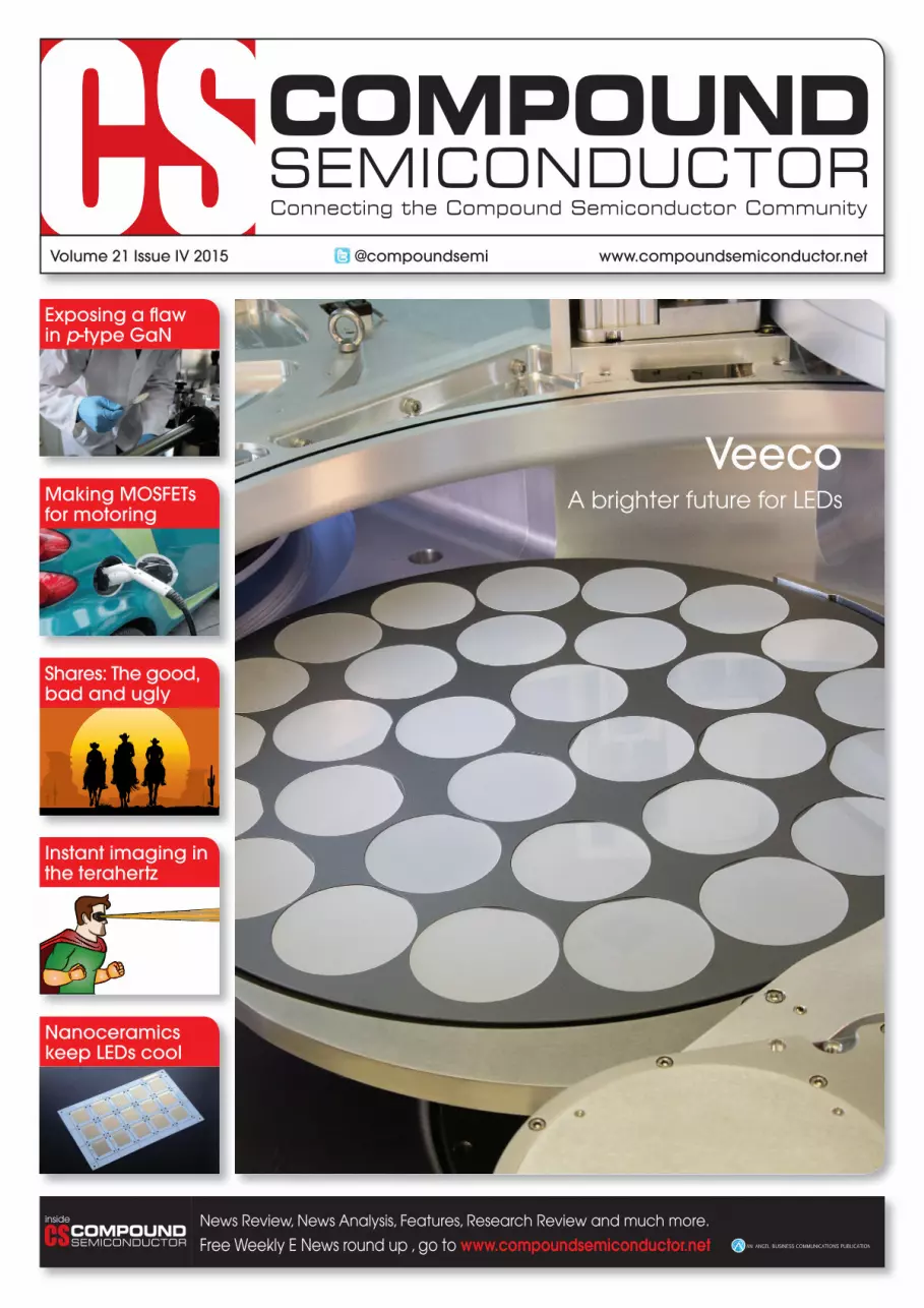
Exposing a flaw in p-type GaN Veeco A brighter future for LEDs Making MOSFETs for motoring Shares: The good, bad and ugly Nanoceramics keep LEDs cool Instant imaging in the terahertz News Review, News Analysis, Features, Research Review and much more. Free Weekly E News round up , go to www.compoundsemiconductor.net Volume 21 Issue IV 2015 @compoundsemi www.compoundsemiconductor.net
Transcript
Exposing a fl awin p-type GaN
VeecoA brighter future for LEDsMaking MOSFETs
for motoring
Shares: The good, bad and ugly
Nanoceramics keep LEDs cool
Instant imaging in the terahertz
News Review, News Analysis, Features, Research Review and much more.
Free Weekly E News round up , go to www.compoundsemiconductor.net
Volume 21 Issue IV 2015 @compoundsemi www.compoundsemiconductor.net
Front Cover CS v5RS.indd 1 28/05/2015 15:09
LCOO_210x297_mm_PDF_X3.indd 2 02.04.15 11:34
Copyright Compound Semiconductor June 2015 www.compoundsemiconductor.net 3
DONALD RUMSFELD, the former US Secretary of State, will be remembered by many for his use of the three following phrases: known knowns, known unknowns and unknown unknowns.
Although we may have a wry smile when we look back at his use of language, we might also find his way of thinking helpful when we consider those mechanisms that are holding back the efficiency of the nitride LED.
Taking this approach, known knowns would include interactions with defects that drag down efficiency, while known unknowns would include droop, given the lack of consensus over its origin.
But what of that third category, the unknown unknown? Well, if something is still not known to anyone, it is impossible to say anything meaningful about it – but we can still consider the recently emerged known unknown, which would have previously been an unknown unknown.
In this issue, we cover one of these in a feature describing the loss in LED efficiency associated with poor p-type layers (see p50). The concern is that p-type layers can appear to be adequate when assessed with a conventional measurement
technique, capacitance-voltage profiling – but when studied by other approaches, they can be found to have high levels of electron concentration, which are responsible for energy-sapping parasitic currents.
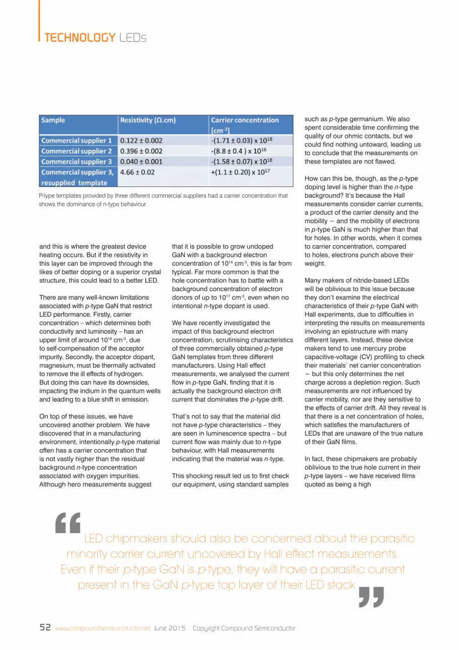
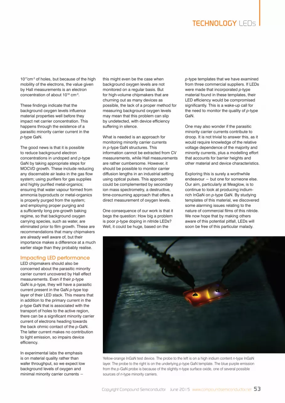
Uncovering this problem were a team of researchers from Lakehead University and Meaglow that had scrutinised p-type GaN templates from three commercial suppliers. In all cases, the background concentration of oxygen was high enough that, judged in terms of carrier concentration, the material was not the expected p-type, but in fact n-type! Note that this can occur when there are more holes than electrons, due to the far higher mobility of the latter charge carrier.
Such a revelation begs a question relating to a now known unknown: How many LED manufacturers are throwing away efficiency, due to high levels of electron concentration in their p-type layers?
I can’t imagine that I will ever get an answer to this, so this will remain a known unknown – but I hope that by highlighting this issue, chipmakers will take the necessary steps to increase the output of their devices.
Editorial View v3RS.indd 3 28/05/2015 15:10
4 www.compoundsemiconductor.net June 2015 Copyright Compound Semiconductor
contentsfeaturesCONNECTING THE COMPOUND SEMICONDUCTOR COMMUNITY Volume 21 Issue IV 2015
24
24 Veeco: Taking and maintaining pole position Veeco’s share of MOCVD sales has soared during the last few years. What is the key to this success?
28 Compound semiconductor shares: The good, the bad and the ugly The last 12 months have produced mixed results for compound semiconductor shares.
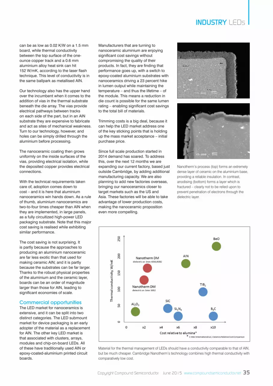
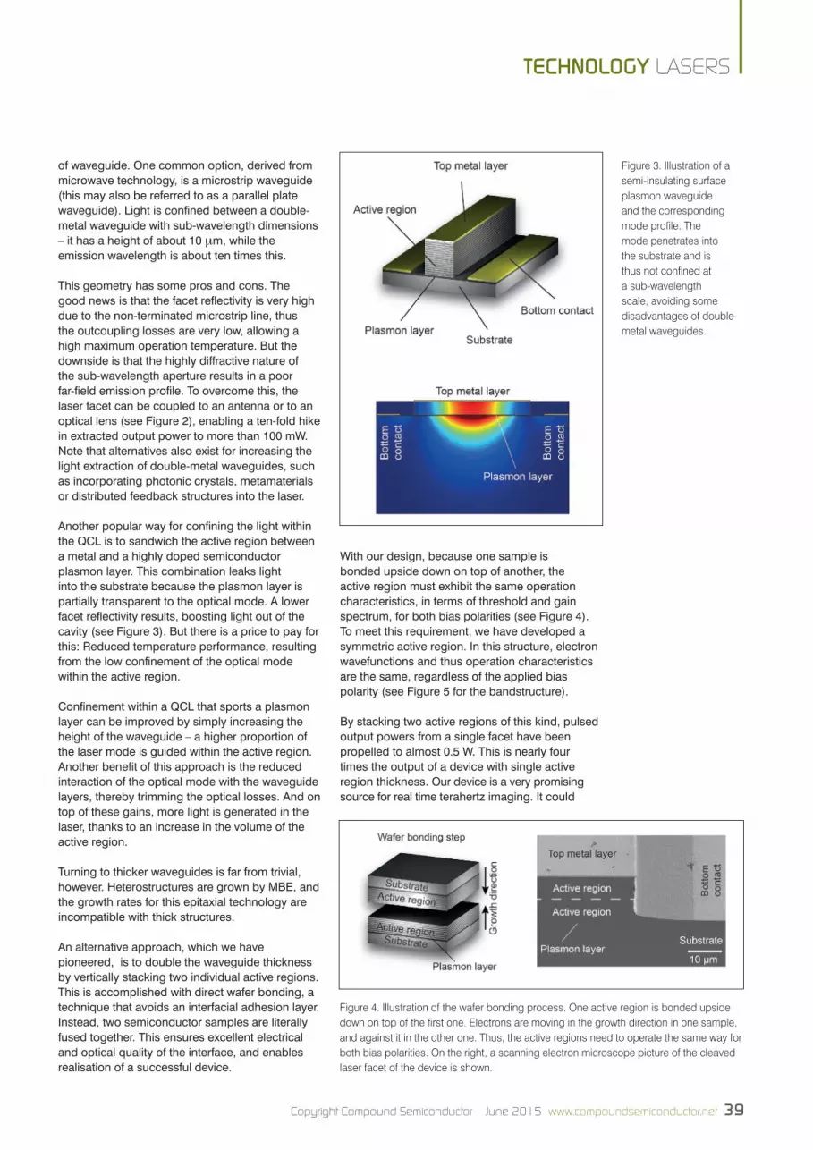
32 LEDs: Keeping cool with nanoceramics Makers of solid-state lighting should turn to aluminium nanoceramics to cut the cost of thermal management
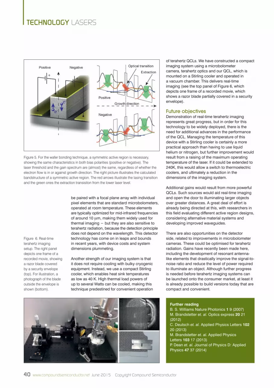
36 Instant imaging with terahertz lasers Wafer-bonding can create powerful terahertz lasers for real-time imaging of hidden weapons, illicit drugs and forms of cancer.
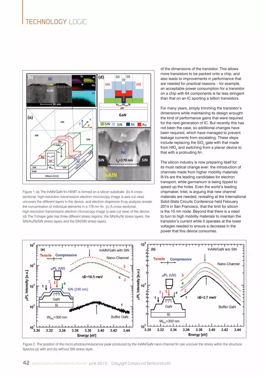
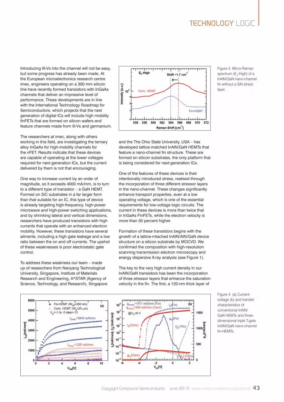
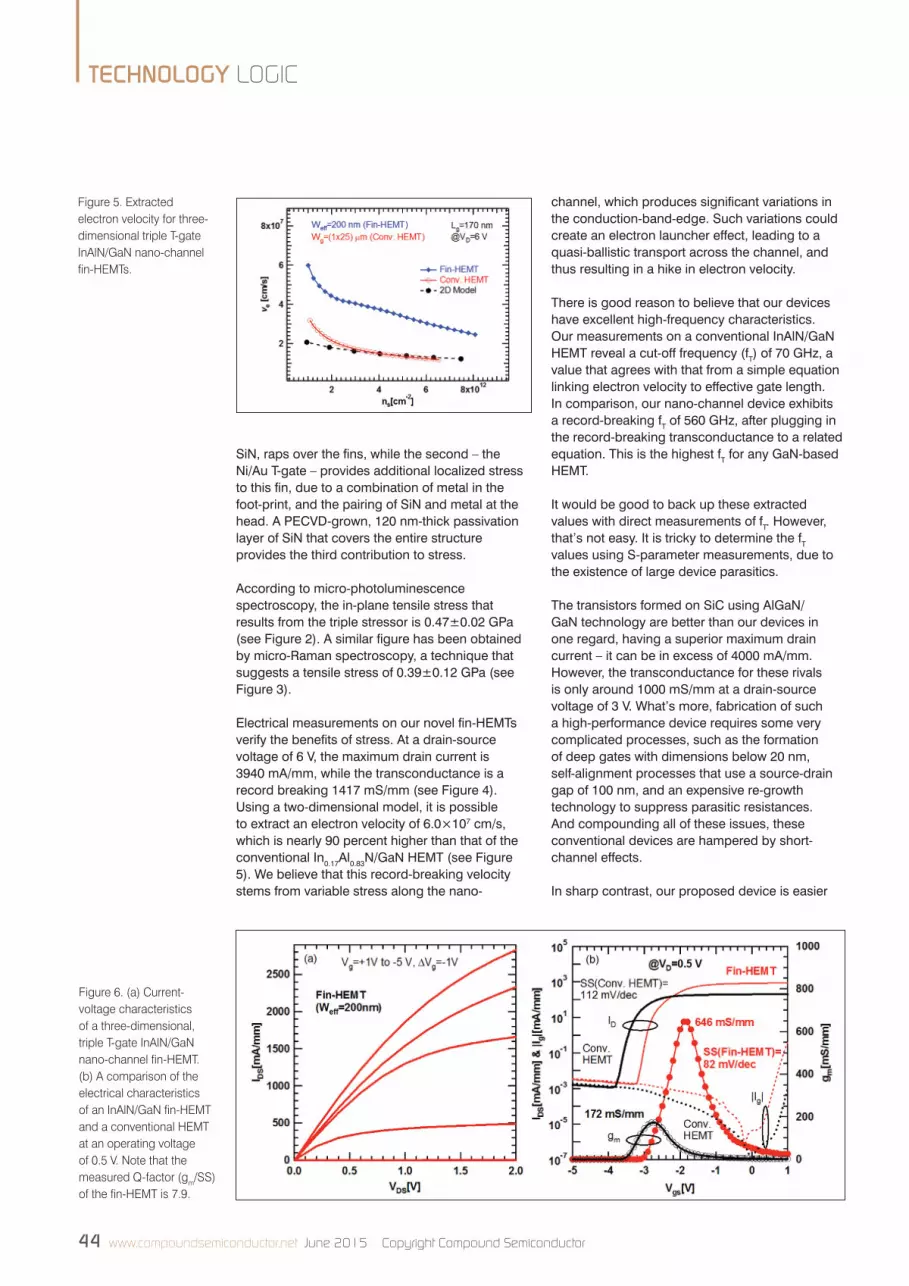
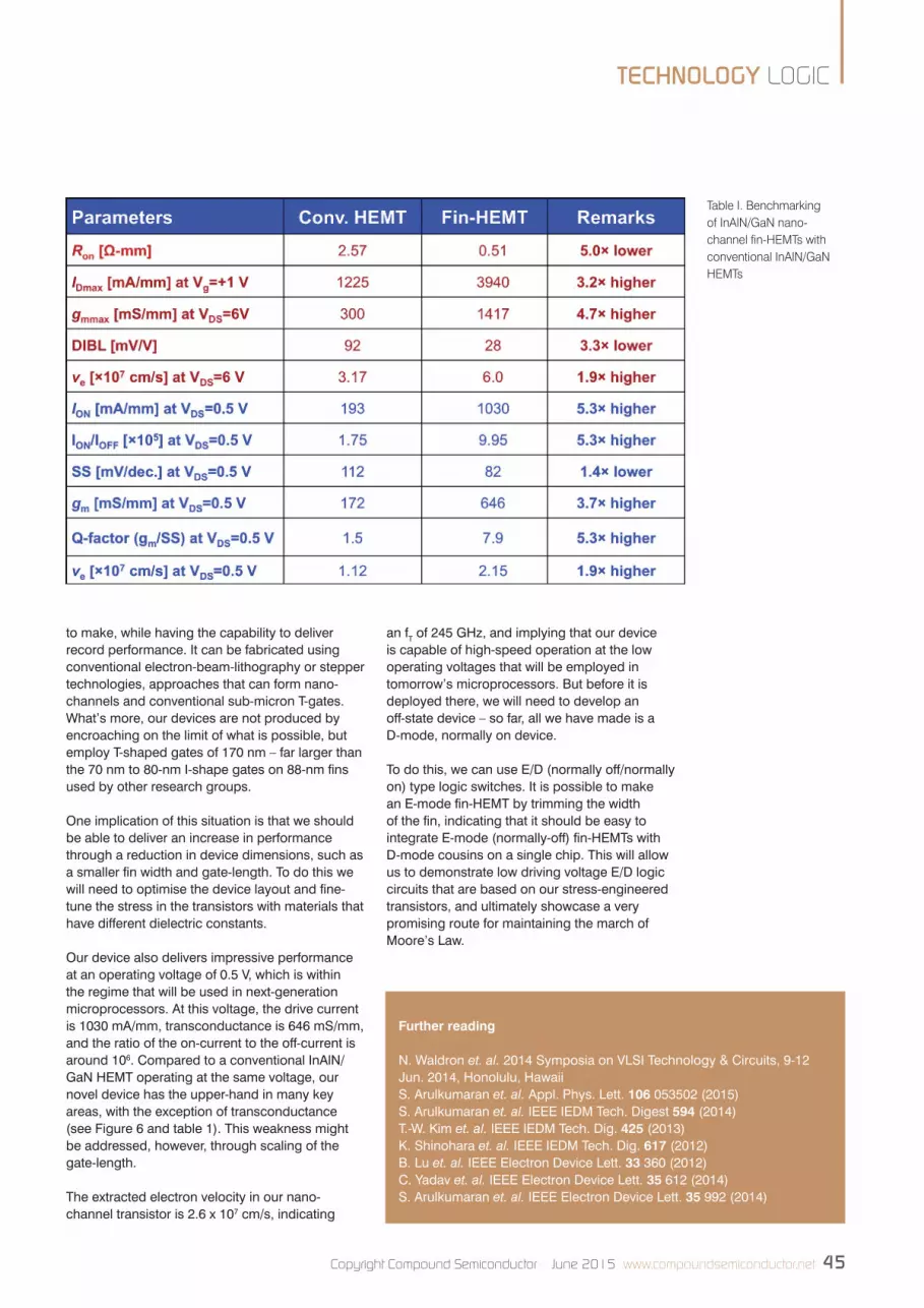
41 GaN: The logical successor to silicon? Stressor layers that crank up the speed of electrons are enabling a novel form of GaN-on-silicon transistor to offer a promising route to maintaining the march of Moore’s law.
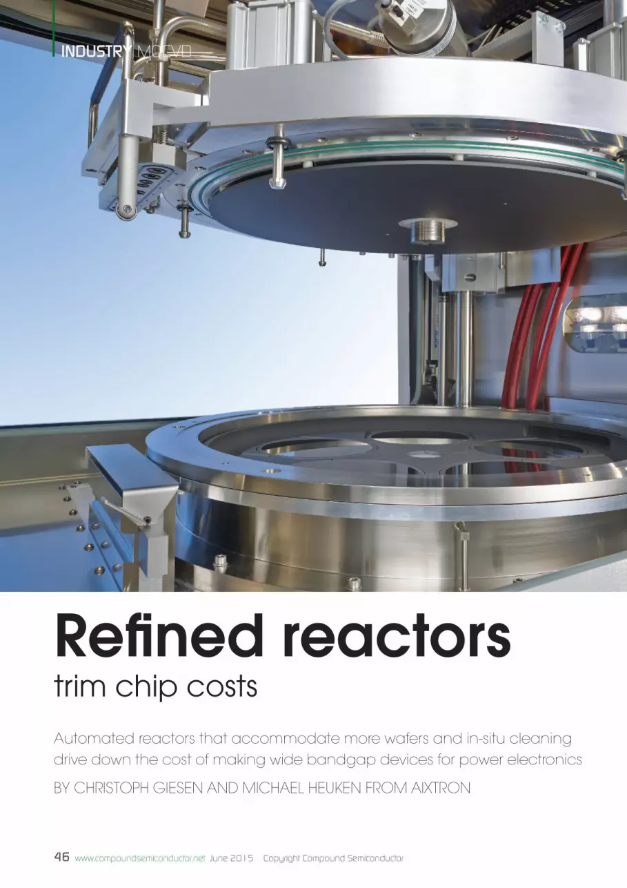
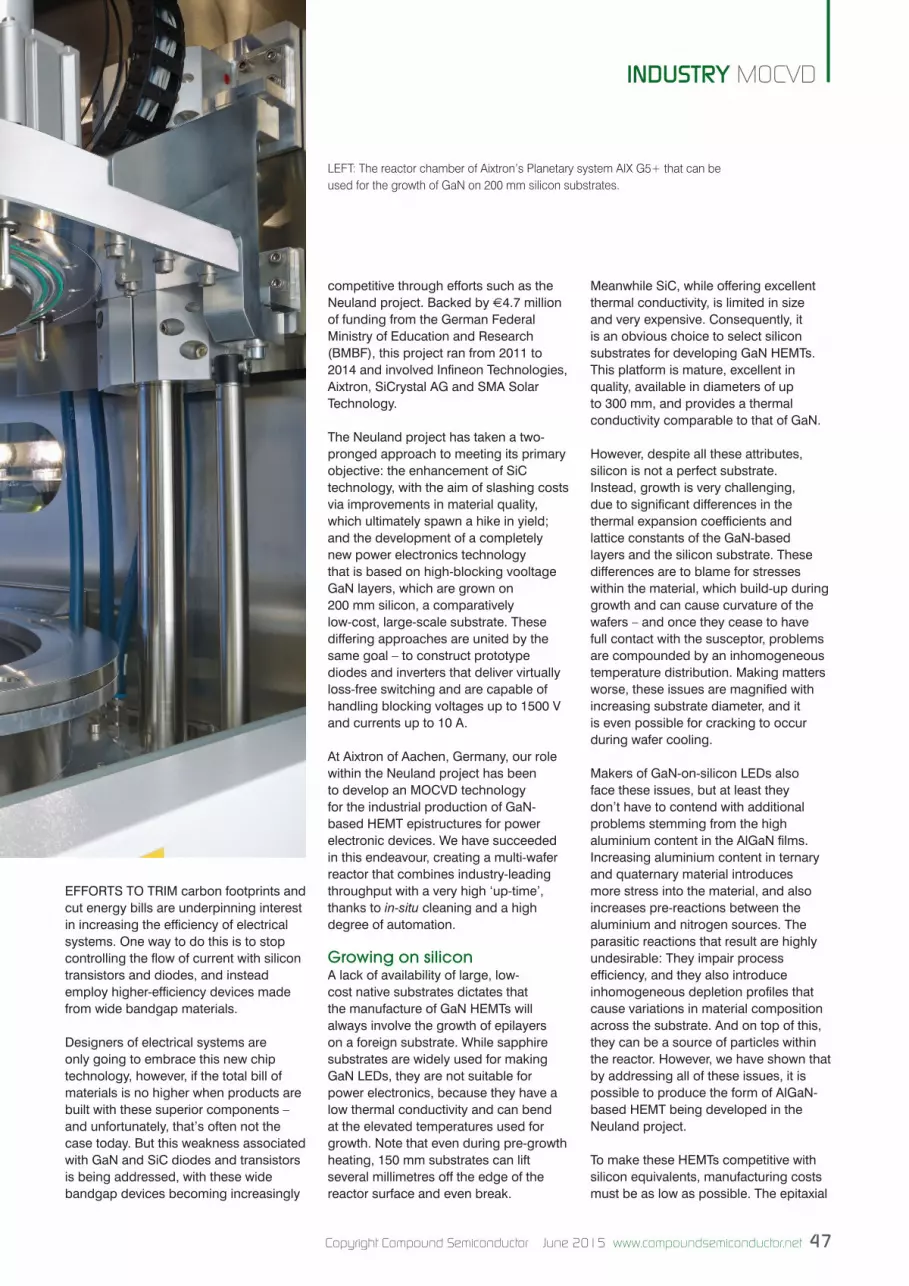
46 Refined reactors trim chip costs Automated reactors that accommodate more wafers and in-situ cleaning drive down the cost of making wide bandgap devices for power electronics.
50 Throwing away LED efficiency Are parasitic currents in p-type layers holding back the efficiency of many commercial LEDs?
Contents v3.indd 4 29/05/2015 15:03
Copyright Compound Semiconductor June 2015 www.compoundsemiconductor.net 5
08 US Energy department awards over $10 million to solid state lighting R&D
09 Cree introduces GaN HEMTs for TWT radar systems
10 £9.5 million initiative to use SiC to modernise UK power grid
13 Cree announces industry’s first 900 V SiC MOSFET
14 TowerJazz and UCSD show 60 GHz wafer-scale phased array transmitter
16 Luminus announces ultra high density COBs LEDs
news analysis 18 Move over silicone
20 LEDs: a potent package
22 Delivering the devices of tomorrow
research review 57 On-resistance falls for vertical GaN MOSFETs
59 Stretching InP VCSELs further into the infrared
61 Unlocking the promise of ultra-wide-bandgap devices
50
Contents v3.indd 5 29/05/2015 15:03
6 www.compoundsemiconductor.net June 2015 Copyright Compound Semiconductor
NEWS REVIEW
Freescale introduces plastic-packaged RF GaN transistorsFREESCALE SEMICONDUCTOR has introduced two ultra-wideband RF power GaN transistors in advanced plastic packages.
“The industry-leading bandwidth of these two products will enable our customers to replace two or even three separate RF PA’s with a single RF line-up, vastly reducing system cost,” said Paul Hart, senior vice president and general manager of Freescale’s RF business. “In addition, the devices’ ultra-low thermal resistance will allow customers to reduce the cost of their cooling systems, or run at full CW-rated power to much higher case temperatures.”
The new OM-270 package, offered in
two-lead and eight-lead configurations, extends Freescale’s proprietary OMNI RF plastic packaging technology to the smallest outline yet, and adds compatibility with GaN.
“We have innovated the capability to metalurgically bond our GaN-on-SiC chips to copper flanges, and over-mold them to enable unprecedented thermal performance,” said Mali Mahalingam, Freescale Fellow and head of RF package development. “In addition, this new package platform supports complex internal matching schemes that enable superior broadband performance.”
The MMRF5015N is a 100W, 50V, true CW ultra-wideband GaN transistor
suited for high power military and civil communication systems. The MMRF5015N has a thermal resistance of less than 0.8°C/W, which represents a more than 30 percent improvement over competitive products. The MMRF5015N is sampling now in an evaluation fixture which demonstrates 200-2500 MHz bandwidth with a minimum of 12dB gain and 40 percent efficiency over the entire band.
MMRF5011N is a 10W, 28V, true CW ultra-wideband transistor, demonstrating 200-2600 MHz bandwidth in an available applications circuit. Suited for lower power military and civil handheld radio communications devices, the MMRF5011 is sampling now.
Cree to spin out power and RF businessLED-MAKER Cree has submitted a draft registration statement to the US Securities and Exchange Commission for a potential initial public offering of the company’s Power and RF subsidiary’s Class A common stock.
The type and number of shares of stock to be sold and the price range for the proposed initial public offering has not yet been determined, although Cree intends to remain the majority stockholder of the subsidiary post offering. The initial public offering is expected to commence after the Securities and Exchange Commission completes its review process, subject to market and other conditions.
The Power and RF subsidiary is raising capital to invest directly in the business to support targeted future growth.
The offering would enable Cree management to focus on Cree’s LED and Lighting businesses, while also creating a dedicated focus on the Power and RF business. The company believes that this transaction should allow Cree shareholders to better realise the full value of both businesses.
QORVO has announced a family of GaN power amplifiers that it says greatly improve the efficiency, gain and power performance of commercial VSAT and military satellite communications.
“Qorvo’s high-performance GaN solutions are providing our customers with next-generation performance needed to meet their evolving system requirements,” said Roger Hall, Qorvo’s general manager of defence and aerospace products. “This latest family of GaN power amplifiers targeting Ku- and Ka-band satellite communications offers the highest combination of output power, gain and efficiency in the market today.”
The TGA 2239-CP Ku-band PA is a 28V device with an output power of 50W. It has 30dB
Qorvo shows new GaN power amplifiers for satellite comms
linear gain and 34 percent power-added efficiency.
For the Ka-band, the TGA2594-HM offers 4W of saturated output power and 25db linear gain in a hermetic, QFN package. The TGA2595-CP offers 8W of saturated output power and 21dB linear gain in a thermally superior Cu-base bolt-down package. Power-added efficiency for both parts are 25 percent and 22 percent respectively. All three amplifiers are made from Qorvo’s production-released QGaN15 process technology.
News CS v2.indd 6 29/05/2015 12:24
Contact Watlow® today for the latest thermal solutions for semiconductor applications.Contact Watlow® today for the latest thermal Contact Watlow® today for the latest thermal Contact Watlow® today for the latest thermal Contact Watlow® today for the latest thermal Contact Watlow® today for the latest thermal Contact Watlow® today for the latest thermal Contact Watlow® today for the latest thermal Contact Watlow® today for the latest thermal Contact Watlow® today for the latest thermal Contact Watlow® today for the latest thermal Contact Watlow® today for the latest thermal Contact Watlow® today for the latest thermal Contact Watlow® today for the latest thermal Contact Watlow® today for the latest thermal Contact Watlow® today for the latest thermal Contact Watlow® today for the latest thermal Contact Watlow® today for the latest thermal Contact Watlow® today for the latest thermal Contact Watlow® today for the latest thermal Contact Watlow® today for the latest thermal Contact Watlow® today for the latest thermal Contact Watlow® today for the latest thermal Contact Watlow® today for the latest thermal Contact Watlow® today for the latest thermal Contact Watlow® today for the latest thermal Contact Watlow® today for the latest thermal Contact Watlow® today for the latest thermal Contact Watlow® today for the latest thermal Contact Watlow® today for the latest thermal Contact Watlow® today for the latest thermal Contact Watlow® today for the latest thermal Contact Watlow® today for the latest thermal Contact Watlow® today for the latest thermal Contact Watlow® today for the latest thermal solutions for semiconductor applications.solutions for semiconductor applications.solutions for semiconductor applications.solutions for semiconductor applications.solutions for semiconductor applications.solutions for semiconductor applications.solutions for semiconductor applications.solutions for semiconductor applications.solutions for semiconductor applications.solutions for semiconductor applications.solutions for semiconductor applications.solutions for semiconductor applications.solutions for semiconductor applications.solutions for semiconductor applications.solutions for semiconductor applications.solutions for semiconductor applications.solutions for semiconductor applications.solutions for semiconductor applications.solutions for semiconductor applications.solutions for semiconductor applications.solutions for semiconductor applications.solutions for semiconductor applications.solutions for semiconductor applications.solutions for semiconductor applications.solutions for semiconductor applications.solutions for semiconductor applications.solutions for semiconductor applications.solutions for semiconductor applications.solutions for semiconductor applications.solutions for semiconductor applications.solutions for semiconductor applications.solutions for semiconductor applications.solutions for semiconductor applications.solutions for semiconductor applications.Contact Watlow® today for the latest thermal Contact Watlow® today for the latest thermal Contact Watlow® today for the latest thermal Contact Watlow® today for the latest thermal Contact Watlow® today for the latest thermal Contact Watlow® today for the latest thermal Contact Watlow® today for the latest thermal Contact Watlow® today for the latest thermal Contact Watlow® today for the latest thermal Contact Watlow® today for the latest thermal Contact Watlow® today for the latest thermal Contact Watlow® today for the latest thermal Contact Watlow® today for the latest thermal Contact Watlow® today for the latest thermal Contact Watlow® today for the latest thermal Contact Watlow® today for the latest thermal solutions for semiconductor applications.solutions for semiconductor applications.solutions for semiconductor applications.solutions for semiconductor applications.solutions for semiconductor applications.solutions for semiconductor applications.solutions for semiconductor applications.solutions for semiconductor applications.solutions for semiconductor applications.solutions for semiconductor applications.solutions for semiconductor applications.solutions for semiconductor applications.solutions for semiconductor applications.
Optimize the Thermal Performance of your
Process Equipment.
Watlow provides innovative
solutions to help process tool
manufacturers meet the needs of the
semiconductor technology roadmap.
Our approach is to work collaboratively
to help solve complex thermal
challenges associated with state-of-the-
art manufacturing processes; helping
to improve yield, throughput and cost
of ownership. This includes innovative
heaters, controllers and sensors for use
in front-end and back-end applications
such as CVD, PECVD, Etch, Diffusion,
Bonding, IC test and more.
Extensive computational tools enable product designs to be highly refined for ultimate performance.
Multi-zone circuit layouts in a polyimide construction are highly customized to deliver exacting performance up to 250°C.
EZ-ZONE® RM Multi-loop controllers are fully scalable with up to 152 PID Loops and 256 monitor points per system.
ASSURANT™ gas and pump line heaters feature high temperature capabilities with low outgassing.
Optimize the Thermal Optimize the Thermal Optimize the Thermal Optimize the Thermal Optimize the Thermal Optimize the Thermal Optimize the Thermal Optimize the Thermal Optimize the Thermal Optimize the Thermal Optimize the Thermal Optimize the Thermal Optimize the Thermal Optimize the Thermal Optimize the Thermal Optimize the Thermal Optimize the Thermal Optimize the Thermal Optimize the Thermal Optimize the Thermal Optimize the Thermal Optimize the Thermal Optimize the Thermal Optimize the Thermal Optimize the Thermal Optimize the Thermal Optimize the Thermal Optimize the Thermal Optimize the Thermal Optimize the Thermal Optimize the Thermal Optimize the Thermal Performance of your Performance of your Performance of your Performance of your Performance of your Performance of your Performance of your Performance of your Performance of your Performance of your Performance of your Performance of your Performance of your Performance of your Performance of your Performance of your Performance of your Performance of your Performance of your Performance of your Performance of your Performance of your Performance of your Performance of your Performance of your Performance of your Performance of your Performance of your Performance of your Performance of your Performance of your Performance of your Performance of your Performance of your Performance of your Performance of your Performance of your Performance of your Performance of your
8 www.compoundsemiconductor.net June 2015 Copyright Compound Semiconductor
NEWS REVIEW
US Energy department awards over $10 million to solid state lighting R&DTHE US ENERGY DEPARTMENT has announced nine research and development projects that will receive funding to support solid-state lighting (SSL) technology research, product development and US manufacturing. The aim is to help accelerate the development of high-quality LED and OLED products that can reduce overall US energy consumption and save consumers money.
Department-funded R&D will foster technology breakthroughs to unlock new levels of performance and energy savings; for example, DOE targets look to increase the efficiency of today’s LEDs by an additional 66 percent. As solid-state electronic technology, LED lighting also offers new potential for advanced lighting control, including colour tuning and intelligent, adaptive lighting.
In total, the nine competitively-selected projects will receive more than $8.2 million and with private sector cost sharing reach a total investment of
more than $11.5 million. “Advances in solid-state lighting technology are critically important for moving the nation closer to a clean energy future, while keeping money in the pocketbooks of American families at the same time,” said Energy Secretary Ernest Moniz. “These Department-funded projects will help tap the full energy-saving potential of solid-state lighting, and create jobs in related industries across the United States.”
Projects selected include: Acuity Brands Lighting (Berkeley, California), which is to develop an organic light-emitting diode that increases efficiency and light output; Cree (Durham, North Carolina) to create a cost-effective, high-efficacy demonstration bulb that renders colours accurately; Philips Research North America (Briarcliff Manor, New York) to develop an innovative LED office lighting system that features controls to maximize energy efficiency and occupant health and well-being; and RTI International (Research Triangle Park, North Carolina) to develop novel designs
for classroom integrated dynamic lighting systems.
This is the tenth round of the Department’s investments in solid-state lighting core technology research and product development, and the sixth round of its investments in US solid-state lighting manufacturing R&D. These efforts are meant to accelerate the adoption of SSL technology through improvements that reduce costs and enhance product quality and performance. For a list of the requested funds by project, please visit the SSL website.
IBM takes a further step towards integrated photonics
IBM ENGINEERS in New York and Zurich, Switzerland and IBM Systems Unit have designed and tested a fully integrated wavelength multiplexed silicon photonics chip, which the company says will soon enable manufacturing of 100Gbps optical transceivers. The chip, the product of 15 years of silicon photonics research, demonstrates transmission and reception of high-speed data using four laser channels each operating as an independent 25Gbps optical channel. The reference design targets datacentre interconnects with a range up to 2km.
“The lasers are brought in from off-chip in order to be modulated, but eventually we hope to incorporate III-V lasers right on the chip,” Will Green, manager of the silicon photonics group at IBM Research told the electronics paper EE Times.Most of the optical interconnect solutions employed within datacentres as of today
are based upon VCSEL technology, where the optical signals are transported via multimode optical fibre.
Demands for increased distance and data rate between ports, due to cloud services for example, are driving the development of cost-effective single-mode optical interconnect technologies, which can overcome the bandwidth-distance limitations inherent to multimode VCSEL links.
IBM say its CMOS Integrated Nano-Photonics Technology provides an economical solution to extend the reach and data rates of optical links. The essential parts of an optical transceiver, both electrical and optical, can be combined monolithically on one silicon chip, and are designed to work with standard silicon chip manufacturing processes.
Cambridge Nanotherm appoints new chairman
LED thermal management company Cambridge Nanotherm has appointed Howard Ford as chairman of the board to help drive the company’s rapid growth into markets in Asia and the US.
Ford has held a number of key roles in high-profile technology companies including chief executive of BT Cellnet, general manager of IBM’s European PC business, and managing director of Equant Network Services before it was acquired by France Telecom in 2005.
In addition to Cambridge Nanotherm, Howard currently holds the position of chairman with Display Data, Pyreos, Light Blue Optics and Filtronic plc.
News CS v2.indd 8 29/05/2015 12:24
Copyright Compound Semiconductor June 2015 www.compoundsemiconductor.net 9
NEWS REVIEW
Pure Silicon Carbide PerfectionVery close customer cooperation has given us a proven excellence in
conductive and semi-insulating Silicon Carbide (SiC) substrates and
epitaxial wafers. A flawless base for semiconductors in the power and
RF electronic industries which results in high quality end products.
Our promise to you: Pure – Clean – Quality
For more information please contact [email protected], www.norstel.com
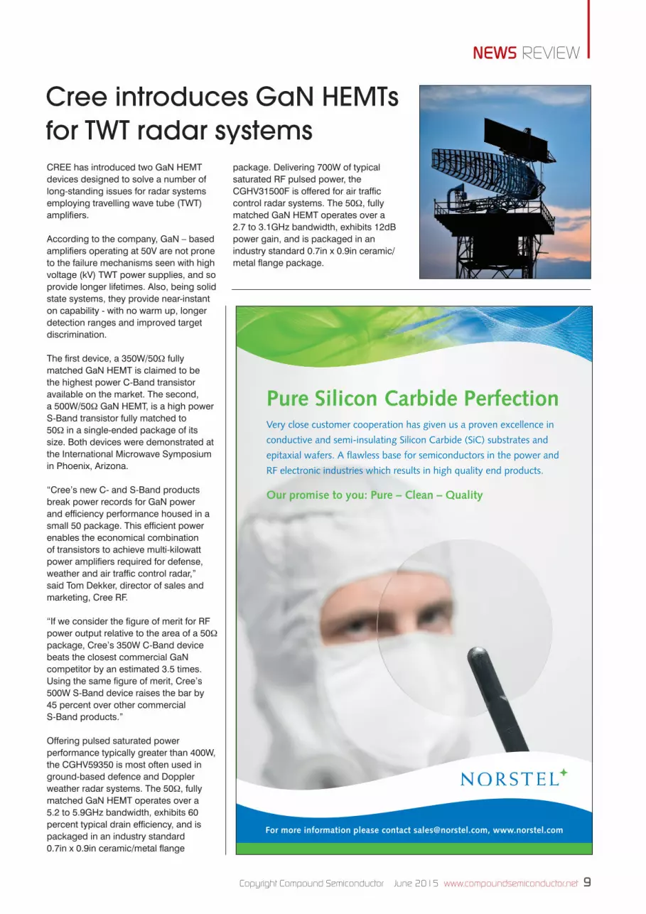
CREE has introduced two GaN HEMT devices designed to solve a number of long-standing issues for radar systems employing travelling wave tube (TWT) amplifiers.
According to the company, GaN – based amplifiers operating at 50V are not prone to the failure mechanisms seen with high voltage (kV) TWT power supplies, and so provide longer lifetimes. Also, being solid state systems, they provide near-instant on capability - with no warm up, longer detection ranges and improved target discrimination.
The first device, a 350W/50Ω fully matched GaN HEMT is claimed to be the highest power C-Band transistor available on the market. The second, a 500W/50Ω GaN HEMT, is a high power S-Band transistor fully matched to 50Ω in a single-ended package of its size. Both devices were demonstrated at the International Microwave Symposium in Phoenix, Arizona.
“Cree’s new C- and S-Band products break power records for GaN power and efficiency performance housed in a small 50 package. This efficient power enables the economical combination of transistors to achieve multi-kilowatt power amplifiers required for defense, weather and air traffic control radar,” said Tom Dekker, director of sales and marketing, Cree RF.
“If we consider the figure of merit for RF power output relative to the area of a 50Ω package, Cree’s 350W C-Band device beats the closest commercial GaN competitor by an estimated 3.5 times. Using the same figure of merit, Cree’s 500W S-Band device raises the bar by 45 percent over other commercial S-Band products.”
Offering pulsed saturated power performance typically greater than 400W, the CGHV59350 is most often used in ground-based defence and Doppler weather radar systems. The 50Ω, fully matched GaN HEMT operates over a 5.2 to 5.9GHz bandwidth, exhibits 60 percent typical drain efficiency, and is packaged in an industry standard 0.7in x 0.9in ceramic/metal flange
Cree introduces GaN HEMTs for TWT radar systems
package. Delivering 700W of typical saturated RF pulsed power, the CGHV31500F is offered for air traffic control radar systems. The 50Ω, fully matched GaN HEMT operates over a 2.7 to 3.1GHz bandwidth, exhibits 12dB power gain, and is packaged in an industry standard 0.7in x 0.9in ceramic/metal flange package.
News CS v2.indd 9 29/05/2015 12:24
10 www.compoundsemiconductor.net June 2015 Copyright Compound Semiconductor
NEWS REVIEW
LED lighting systems to exceed 4.1 billion a year by 2024
A NEW REPORT from Navigant Research forecasts that worldwide shipments of LED lamps and modules will grow from 864 million annually in 2015 to more than 4.1 billion by 2024.
The report LED Lighting: Global Outlook analyses the world market for light-emitting diode (LED) lamps and modules across all major space lighting uses.
“Early adopters were attracted by some of the unique features of LED lighting, such as improved efficiency, improved operation in cold environments, and enhanced controllability,” says Jesse Foote, senior research analyst with Navigant Research. “The current wave of adoption, by contrast, is much more focused on the value of ongoing energy savings compared to a relatively modest increase in upfront cost.”
While Europe has perhaps led the way on residential energy efficiency, according to the report, incandescent bans and minimum efficacy levels for bulbs are being introduced throughout the globe.In North America, the Energy Independence and Security Act (EISA)-which requires 25 percent greater efficiency for light bulbs, phased in from 2012 through 2014-is in full swing, and the Canadian equivalent is not far behind.
The laws of physics make it almost impossible for a manufacturer to design a bulb that is as efficient as a compact fluorescent light or LED.
Navigant Research provides market research and benchmarking services for rapidly changing and often highly regulated industries.
£9.5 million initiative to use SiC to modernise UK gridANVIL SEMICONDUCTORS has announced its participation in a £9.5 million government initiative to modernise the UK energy infrastructure to cope with the unprecedented change in energy consumption, generation and distribution. Innovate UK, the UK technology strategy board, is funding projects that drive innovative ways in how energy is supplied and used to address the energy challenges of sustainability, security of supply and affordability.
This project, trialled on Western Power Distribution’s residential network will use Anvil’s SiC-on-silicon power devices to look to increase the UK’s energy network capacity to tackle residential and commercial needs. The team comprises Western Power Distribution, Anvil Semiconductors, Turbo Power Systems, Aston University, Exception EMS and Schneider Electric in the design and delivery of this project.
By 2020 the UK is expected to have 10 million homes with solar panels and the number of electric vehicles sold will increase to 6.4 million by 2023. As a result the existing energy infrastructure, designed for a one way flow of energy, will have to deal with unprecedented patterns in network load.
The challenge of integrating distributed power generation, with traditional larger scale energy generation presents new risks in terms of voltage control and predicting load and demand. Distribution Network Operators (DNOs) are facing significant challenges in modernising existing infrastructure, and investing in smart technologies, to
cope with this transformation. The trial aims to deliver a dramatic increase in the capacity of our existing residential energy infrastructure, by increasing the local network voltage. This approach will allow the grid to simultaneously deliver different voltages for different requirements (i.e. charging an electric car and simultaneously providing a constant 240V for a residential building).
This project will trial the installation of high-performance power electronic converters (PECs) into the meter-box of individual properties and a local substation converter for distributing at 400V. In order to achieve the required level of performance, efficiency, stability and sustainability at the cost demanded, these PECs will use innovative low cost SiC switching devices built using Anvil’s SiC-on-silicon technology.
Anvil Semiconductors, which is backed by Business Angels and early stage VCs, was established in August 2010 to
develop SiC power devices for the power electronics
industry. Anvil’s approach enables the growth of device quality 3C-SiC epitaxy on 100mm diameter silicon wafers to thicknesses that permit the fabrication of vertical power devices.
The proprietary process overcomes mismatches in lattice parameter and thermal coefficient of expansion and can be readily migrated onto 150mm wafers and potentially beyond.
The company has offices in Coventry and Cambridge and has a small experienced team and
a network of industrial and academic partners.
News CS v2.indd 10 29/05/2015 12:24
“Now offering Germanium Reclaim”
Growth and device fabrication of arsenide/antimonide based III-V semiconductors notably:
• Narrow bandgap materials (InSb up to AlAs) • Antimonide doping capability • InGaAs/AlInAs structures lattice matched to InP
substrates • AlInGaAsSb lattice matched to InAs, GaSb or InP
substrates • Quantum dots/wells on GaAs substrates • Antimonides on GaAs substrates using relaxed
Supplier of low volume wafer requirements. Research work enquiries welcome.
MBE GROWTH SPECIALISTS
Untitled-2 1 28/05/2015 12:38
www.evatecnet.com
LEDs • ADVANCED PACKAGING • POWER DEVICES • MEMS • TELECOMS • PHOTOVOLTAICS • EVATEC - THE THIN FILM POWERHOUSE
COMPLETE THIN FILM DEP & ETCH SOLUTIONS
MORE INFO
Let Evatec engineers help you solve your manufacturing puzzles. From raising
throughput in Under Bump Metallisation (UBM) processes on 12 inch, to delivering
plasma damage free sputter processing on GaN for LEDs and Power Devices,
Evatec platforms with Advanced Process Control (APC) raise yields and lower
Cost of Ownership. For more information about Evatec visit our website at
www.evatecnet.com or contact your local sales agent.
The Micro and Nanotechnology Laboratory at the University of Illinois at Urbana-Champaign seeks applicants for a Research Engineer to promote research related activities by managing equipment involving semiconductor device fabrication, processes, and some applications in nano-biotechnology. Information about the Micro and Nanotechnology Laboratory can be found here: http://mntl.illinois.edu/.
Please visit http://jobs.illinois.edu to view the complete position announcement and application instructions. The closing date for this position is June 30, 2015. Illinois is an EEO Employer/Vet/Disabled - www.inclusiveillinois.illinois.edu
Research EngineerMicro and Nanotechnology LaboratoryCollege of Engineering
University of Illinois at Urbana-Champaign
New CS APP ready for Download NOW!
Wafer-bonding for telco VCSELs
GaN HEMTsDitching the package
Extending the life of fab tools
GaAs will fend off the CMOS threat
UCSB: Auger causes LED droop
Scrutinizing GaN HEMT interfaces
News Review, News Analysis, Features, Research Review and much more.
Free Weekly E News round up , go to www.compoundsemiconductor.net
News Review, News Analysis, Features, Research Review and much more.
Free Weekly E News round up , go to www.compoundsemiconductor.net
Volume 19 Issue 4 2013 @compoundsemi
www.compoundsemiconductor.net
Continuing our aim of ‘connecting the compound semiconductor industry’, Compound Semiconductor has a Free app for Android, iPhone and iPad to allow you keep up to date wherever you are.
Available FREE from the App Store or Google Play, the app allows you to access: Latest Compound Semiconductor, CS China and CS Taiwan magazines Latest features Latest news and more...
Copyright Compound Semiconductor June 2015 www.compoundsemiconductor.net 13
NEWS REVIEW
CREE has introduced what it believes is the industry’s first 900V SiC MOSFET range. Designed for high frequency power electronics applications, including renewable energy inverters, electric vehicle charging systems, and three-phase industrial power supplies, the 900V platform enables smaller and higher efficiency next-generation power conversion systems at cost parity with silicon-based solutions.
“As a technology leader in SiC power, we’re committed to breaking the performance barriers that really matter to the power conversion design community,” said Cengiz Balkas, vice president and general manager, Cree Power and RF.
He added: “When compared to equivalent silicon MOSFETs, this breakthrough 900 V platform enables a new market for our products by broadening the power range we can address in end systems. Following our 1200 V MOSFETs, which exhibit superior performance to high voltage IGBTs, we are now able to outperform lower
voltage superjunction silicon MOSFET technology at 900 V.”
Built on Cree’s SiC planar technology, the new 900 V MOSFET platform expands the product portfolio to address design challenges common to new and evolving application segments in which a higher DC link voltage is desirable.
According to Cree, existing 900 V silicon MOSFETs have severe limitations for high frequency switching circuits due to switching losses and poor internal body diodes. Further limiting the use of silicon MOSFETs is the Rds(on) that increases 3X over temperature, which causes thermal issues and significant derating. Alternately, Cree’s new 900 V MOSFET technology delivers low Rds(on) at higher temperatures, enabling a significant size reduction of the thermal management system.
The lead product (C3M0065090J) features a low on-resistance rating of 65mΩ. At higher temperature operation (TJ = 150°C), the Rds(on) is just 90mΩ.
Cree announces industry’s first 900V SiC MOSFET
SiC junction transistors diodes offered in mini-module
GENESIC SEMICONDUCTOR, a US developer of SiC power semiconductors, has announced the availability of 20mΩ-1200V SiC junction transistor-diodes in an isolated, 4-Leaded mini-module packaging.
“GeneSiC’s SiC transistor and rectifier products are designed and manufactured to realize low on-state and switching losses. A combination of these technologies in an innovative package promises exemplar performance in power circuits demanding wide bandgap based devices. The mini-module packaging offers great design flexibility for use in a variety of power circuits like H-Bridge, Flyback and multi-level inverters” said Ranbir Singh, President of GeneSiC Semiconductor.
The diodes enable low turn-on energies losses while offering flexible, modular designs in high frequency power converters, according to the company. Co-packaged SiC junction transistors (SJT)-SiC Rectifiers offered by GeneSiC are applicable to switching applications such as induction heaters, plasma generators, fast chargers, DC-DC converters, and switched mode power supplies.
According to the company, SJTs are the only widebandgap switch to offer more than10 µsec repetitive short circuit capability, even at 80 percent of the rated voltages (e.g. 960V for a 1200V device).
In addition to the sub-10ns rise/falls times and a square reverse biased safe operation area, the Gate Return terminal in the new configuration significantly improves the ability to reduce the switching energies. These new class of products offers transient energy losses and switching times that are independent of junction temperature.
Translucent and Vilnius link up for non polar GaNTranslucent Inc, based in Palo Alto, US, has announced a joint project with Vilnius University developing non-polar GaN epitaxy on Translucent’s cREO silicon templates.
Translucent’s epi-Twist substrates will be used by the Institute of Applied Research at Vilnius University, Lithuania for MOCVD growth of non-polar GaN. The group received €119.9K research grant from Research Council of Lithuania.
The crystalline rare earth oxide (cREO) epitaxially grown on silicon is a proven template for the MOCVD growth of III-N materials. Available in both 150mm and 200mm diameters, these templates provide an entry point for new adopters of power GaN supporting both AlN first MOCVD but also enabling GaN first growth processes not currently
available for MOCVD growth on silicon. Since the template is grown independently of the III-N its properties can be designed to support the upstream MOCVD process – for example the buried oxide can take a portion of the vertical breakdown or can be used to offset some of the mechanical stresses imparted traditional GaN-on-silicon. Focused on serving the power GaN market this technology also has applicability to both RF GaN and GaN LEDs on silicon.
The goal of the project is to demonstrate MOCVD growth of non-polar GaN on Si(100). Initial research results in this field, previously conducted by Translucent, were presented at IWN-2014 in Wroclaw, Poland. The Vilnius project is currently funded through September 2017.
News CS v2.indd 13 29/05/2015 12:24
14 www.compoundsemiconductor.net June 2015 Copyright Compound Semiconductor
NEWS REVIEW
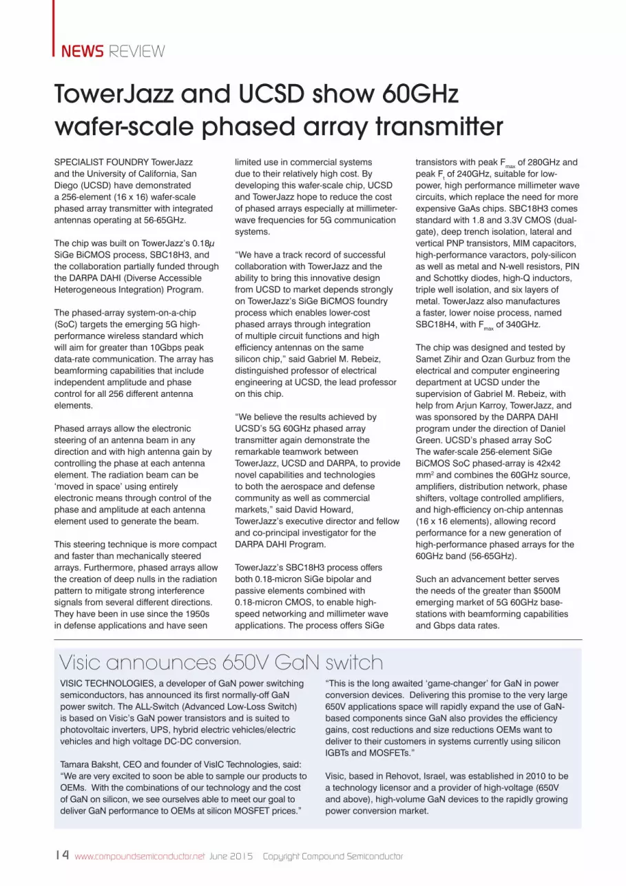
VISIC TECHNOLOGIES, a developer of GaN power switching semiconductors, has announced its first normally-off GaN power switch. The ALL-Switch (Advanced Low-Loss Switch) is based on Visic’s GaN power transistors and is suited to photovoltaic inverters, UPS, hybrid electric vehicles/electric vehicles and high voltage DC-DC conversion.
Tamara Baksht, CEO and founder of VisIC Technologies, said: “We are very excited to soon be able to sample our products to OEMs. With the combinations of our technology and the cost of GaN on silicon, we see ourselves able to meet our goal to deliver GaN performance to OEMs at silicon MOSFET prices.”
“This is the long awaited ‘game-changer’ for GaN in power conversion devices. Delivering this promise to the very large 650V applications space will rapidly expand the use of GaN-based components since GaN also provides the efficiency gains, cost reductions and size reductions OEMs want to deliver to their customers in systems currently using silicon IGBTs and MOSFETs.”
Visic, based in Rehovot, Israel, was established in 2010 to be a technology licensor and a provider of high-voltage (650V and above), high-volume GaN devices to the rapidly growing power conversion market.
SPECIALIST FOUNDRY TowerJazz and the University of California, San Diego (UCSD) have demonstrated a 256-element (16 x 16) wafer-scale phased array transmitter with integrated antennas operating at 56-65GHz.
The chip was built on TowerJazz’s 0.18µ SiGe BiCMOS process, SBC18H3, and the collaboration partially funded through the DARPA DAHI (Diverse Accessible Heterogeneous Integration) Program.
The phased-array system-on-a-chip (SoC) targets the emerging 5G high-performance wireless standard which will aim for greater than 10Gbps peak data-rate communication. The array has beamforming capabilities that include independent amplitude and phase control for all 256 different antenna elements.
Phased arrays allow the electronic steering of an antenna beam in any direction and with high antenna gain by controlling the phase at each antenna element. The radiation beam can be ‘moved in space’ using entirely electronic means through control of the phase and amplitude at each antenna element used to generate the beam.
This steering technique is more compact and faster than mechanically steered arrays. Furthermore, phased arrays allow the creation of deep nulls in the radiation pattern to mitigate strong interference signals from several different directions. They have been in use since the 1950s in defense applications and have seen
limited use in commercial systems due to their relatively high cost. By developing this wafer-scale chip, UCSD and TowerJazz hope to reduce the cost of phased arrays especially at millimeter-wave frequencies for 5G communication systems.
“We have a track record of successful collaboration with TowerJazz and the ability to bring this innovative design from UCSD to market depends strongly on TowerJazz’s SiGe BiCMOS foundry process which enables lower-cost phased arrays through integration of multiple circuit functions and high efficiency antennas on the same silicon chip,” said Gabriel M. Rebeiz, distinguished professor of electrical engineering at UCSD, the lead professor on this chip.
“We believe the results achieved by UCSD’s 5G 60GHz phased array transmitter again demonstrate the remarkable teamwork between TowerJazz, UCSD and DARPA, to provide novel capabilities and technologies to both the aerospace and defense community as well as commercial markets,” said David Howard, TowerJazz’s executive director and fellow and co-principal investigator for the DARPA DAHI Program.
TowerJazz’s SBC18H3 process offers both 0.18-micron SiGe bipolar and passive elements combined with 0.18-micron CMOS, to enable high-speed networking and millimeter wave applications. The process offers SiGe
transistors with peak Fmax of 280GHz and peak Ft of 240GHz, suitable for low-power, high performance millimeter wave circuits, which replace the need for more expensive GaAs chips. SBC18H3 comes standard with 1.8 and 3.3V CMOS (dual-gate), deep trench isolation, lateral and vertical PNP transistors, MIM capacitors, high-performance varactors, poly-silicon as well as metal and N-well resistors, PIN and Schottky diodes, high-Q inductors, triple well isolation, and six layers of metal. TowerJazz also manufactures a faster, lower noise process, named SBC18H4, with Fmax of 340GHz.
The chip was designed and tested by Samet Zihir and Ozan Gurbuz from the electrical and computer engineering department at UCSD under the supervision of Gabriel M. Rebeiz, with help from Arjun Karroy, TowerJazz, and was sponsored by the DARPA DAHI program under the direction of Daniel Green. UCSD’s phased array SoCThe wafer-scale 256-element SiGe BiCMOS SoC phased-array is 42x42 mm2 and combines the 60GHz source, amplifiers, distribution network, phase shifters, voltage controlled amplifiers, and high-efficiency on-chip antennas (16 x 16 elements), allowing record performance for a new generation of high-performance phased arrays for the 60GHz band (56-65GHz).
Such an advancement better serves the needs of the greater than $500M emerging market of 5G 60GHz base-stations with beamforming capabilities and Gbps data rates.
TowerJazz and UCSD show 60GHz wafer-scale phased array transmitter
Visic announces 650V GaN switch
News CS v2.indd 14 29/05/2015 12:24
your!EPITAXIAL GROWTH!
partner!
Enabling advanced technologiesWorld leading technology
Complete materials range
MOCVD, MBE, CVD
Advanced semiconductor wafer products
Advanced R&D capabilities
Multiple, manufacturing sites (Europe, Asia, USA)
www.iqep.com
Untitled-1 1 02/07/2014 11:05
16 www.compoundsemiconductor.net June 2015 Copyright Compound Semiconductor
NEWS REVIEW
8 benefits of sponsoring CS International 2016
Connecting, informing and inspiring the compound semiconductor industry
CALL NOW: +44 (0)24 76718970email [email protected] or view the online
sponsorship pack at mediapack.cs-international.net
www.cs-international.net
ü Senior management networking opportunities
ü Increased company and brand awareness
ü Access to the top strategists within the compound semiconductor industry
ü Create, develop and support customer relationships
ü Engage in debate, share insight and expertise on industry challenges
ü Gain visibility and recognition as an industry leader
ü Leverage exposure in multiple industry media
ü Demonstrate market innovation and leadership by launching new services, products and systems
Luminus announces ultra high density COBs LEDsLUMINUS, a US-based manufacturer of high-performance LEDs, has announced a new family of ultra- high density chip on board (COB) arrays designed to replace ceramic metal halide technology commonly used in spot lights for retail lighting.
The new XH series COBs are available in a variety of standard light emitting
surface diameters including 6, 9, 11, and 14mm, which means that customers can use their existing ecosystems for optics and connectors, while producing new bulbs and fixtures with higher lumen output and increased centre beam candle power(CBCP).
The 9mm and 11 mm XH series COBs deliver the lumen output and high quality
MACOM introduces 6W power amplifierMACOM has introduced a high linearity 6W power amplifier, suited for Ka-Band high data density satellite communications and 5G radio access networks.
The MAAP-011140-DIE is offered as a bare die, delivering 24dB of linear gain, 6W of saturated output power and 23 percent power-added efficiency.
“The MAAP-011140-DIE offers a unique combination of high power, linearity and efficiency in a small form factor that is ideally suited to systems requiring highly efficient Satcom transmitter solutions,” said Paul Beasly, product manager. “In conjunction with the recently announced 4W Ka-Band PA, MAAP-011139-DIE this new 6W device broadens MACOM’s Ka-Band power amplifier family.”
The device provides greater than 25dBm POUT/tone while maintaining IM3 levels of 30dBc. The efficiency performance allows customers to operate remote VSAT terminals with lower power consumption and higher performance than competing alternative offerings. The 6W PSAT enables greater transmission power and signal strength performance in critical military or civilian datalink applications.
of light to replace 39W and 70W metal halide sources respectively. With a tiny form factor, the 6mm XH series at 3000K 80CRI generates 1500 lumens, and when combined with a 85mm diameter optic, throws an 8 degree beam with CBCP of over 30,000 Cd.
David Davito, product marketing director at Luminus, notes: “The high lumen density of our XH series is enabling our customers to replace metal halide by taking advantage of our high quality of light and shaping the beam into narrow spots with high CBCP while still maintaining small form factors in their bulb and luminaire designs. This results in more attractive retail displays where spot lights with more ‘punch’ will draw the consumers’ eyes to targeted garments and merchandise, while also reducing energy bills, of course.”
News CS v2.indd 16 29/05/2015 12:25
Change is Here. Propel into a Cleaner Future.
PowerGaN MOCVD
The Future of Electric Vehicles, Alternative Energy and More Change Driven by GaN Power DevicesAdvances in MOCVD technology are resulting in major breakthroughs for power IC R&D markets. Compound semiconductor based power electronic devices show enormous potential in delivering cost-effective and energy-efficient solutions for a broad range of applications, including automotive, solar and wind power, consumer electronics, power supplies and IT servers. Veeco is propelling these advancements with an entirely new MOCVD platform.
Veeco is Enabling Power Electronics With Excellent Yield and Superior Film QualityVeeco’s Propel™ PowerGaN™ MOCVD system, designed specifically to advance the power electronics industry, features a single-wafer reactor platform that is capable of processing six and eight-inch wafers. The Propel system deposits high-quality GaN films for the production of highly-effective power electronic devices.
Learn more at www.veeco.com/Propel.
Untitled-1 1 26/05/2015 09:15
18 www.compoundsemiconductor.net June 2015 Copyright Compound Semiconductor
NEWS ANALYSIS LEDs
move over s i l i c o n e
Will new LED packages deliver better device efficiencies? Finland-based Inkron promises this and more, reports Rebecca Pool.
AT A TIME WHEN LED manufacturers are looking to squeeze every last ounce of performance out of their chips, many in the industry are turning to packaging to boost device efficiencies further. Today’s high-brightness LEDs typically come wrapped up in a robust, silicone encapsulant, but is this still enough?
On the plus side, the material provides optical clarity when exposed to heat and humidity, offering solid photo-thermal stability throughout an LED’s lifetime. It also delivers high optical transmittance in the UV-visible wavelength regions, ensuring LED light is transmitted efficiently through the silicone material.
Crucially, the material can be synthesized as a single-chain polymer with a range of different attached organic groups, to tailor its refractive index and boost light-extracting efficiency. But as LED technology matures and demands for
ever-higher efficiencies continue to grow, industry wants more.
As Juha Rantala, chief executive of Inkron, a Finland-based developer of pastes, inks and dielectrics for electronics devices, puts it: “Our view is that the LED efficiency improvements so far have been coming from the chip, and this is now running out of steam.”
“Chip efficiencies are getting closer and closer to physical limits, so now we believe performance improvements must come from the packaging,” he adds. “Thermal efficiency, heat dissipation, heat removal and light extraction all need to be addressed at the packaging level.”
LED focusRantala’s company has already developed a host of die attach pastes,
dielectrics, encapsulants and more for power electronics, organic LEDs and other devices, but now the company is intent on cracking the high-brightness LED market.
“We’ve seen a lot interest coming from [manufacturers of LEDs for] general lighting and automotive applications,” he says. “Right now the traditional silicone package market is dominated by Shin-Etsu and Dow Corning, but there is a need for innovation.”
“[Customers] don’t like the fact that there are only two suppliers, and are really looking for alternative solutions,” he adds.Which, of course, is where Inkron’s latest product comes in. The company has developed a siloxane-based
News Analysis v5_RS.indd 18 29/05/2015 12:26
Copyright Compound Semiconductor June 2015 www.compoundsemiconductor.net 19
NEWS ANALYSIS LEDs
strength to protect and support the die in vastly cheaper wafer-level and chip-scale packaging processes. Traditional packaging currently represents up to 40 percent of the overall LED cost while figures from LumiLEDs suggest a move to chip-scale packaging would obliterate these costs, leaving LEDs at least 30 percent cheaper.
Rantala also reckons industry interest in alternative LED substrates could drive development towards chip-scale packaging. “The industry has been dominated by chip volumes that are sapphire-based, and there’s so much manufacturing capacity here,” he says. “But we’ve been talking to, for example, Japan-based companies that are [considering] GaN-on-silicon LEDs, and they are looking at chip-scale packaging.”
So where is Inkron right now? The company currently offers testing services, and now intends to scale up in-house production to meet current customer demands.
Throughout the last two months, the company has been sampling materials for LED applications and its focus will remain here for the foreseeable future. As Rentala says: “We’re also working on power electronics applications, but the qualification time for power devices can take two years. We can qualify LEDs in three-to-six months, which is important in terms of cash flow for a young company.”
But as the chief executive asserts, he is open to either re-locating production from Finland to Asia, which is where the lion-share of LED packaging takes place, or partnering with a company in this region.
“We are seeing a demand for new materials in this industry, in the same way we saw this in the semiconductor industry ten years ago,” he adds. “Siloxane materials with nanoparticles is the right approach, but we are realistic and know we, alone, can’t handle the volumes that could come from this market.”
encapsulation resin designed for LED applications.
According to Rantala, the material offers excellent UV and thermal stability, providing a better barrier to air, water and sulphur, than conventional silicone packaging, and delivering some two-and-a-half times more resistance to these environmental influences.
And, while the refractive index of your typical silicone encapsulant comes in at around 1.4, Inkron’s material will provide a higher refractive index of 1.6. This figure is closer to the refractive index of the LED industry’s favourite substrate, sapphire, enhancing light output from the substrate to the encapsulant, and according to Inkron, boosting light output efficacy by up to 10 percent.
What’s more, the company can disperse nanoparticles into the siloxane polymer to raise the refractive index to 1.8, which could boost efficacy by up to a further 15 percent, without any loss in light transmission.
“We have a product roadmap to reach a refractive index of 1.8 in the future, but first we want to go to market with our lower refractive index material, and then highlight to clients that if they want more light extraction in the future, our platform is compatible with this,” he explains.And, while siloxane-based material can be used to increase the performance of today’s discrete LED packages, unlike current silicones, it has the mechanical
20 www.compoundsemiconductor.net June 2015 Copyright Compound Semiconductor
NEWS ANALYSIS LEDs
LEDs: a potent packageIn the race to cut manufacturing costs and win market share, Plessey unveils bold plans for bigger wafers, chip-scale packaging and more. Rebecca Pool investigates.
AS THE LED LIGHTING REVOLUTION shines on, industry players are now focusing on cutting manufacturing costs to drive LEDs further into the general lighting market. Today, GaN-on sapphire is the mainstream technology for LED manufacturing but industry interest in GaN-on-silicon is rising.
Clearly the cheaper silicon substrate holds appeal, but the opportunity to manufacture on amortized 6-inch and 8-inch CMOS lines is where the real
interest lies, a fact that hasn’t been lost on LED manufacturer, Plessey. The UK’s leading LED light has been fabricating GaN-on-silicon LEDs on 6-inch wafers from its Plymouth plant − originally a 6-inch CMOS line − for at least two years, and is now looking at the next step.
“Our programme of work on eight inch substrates starts next month,” says Keith Strickland, chief technology officer from Plessey. “There’s no significant technical hurdles to overcome, it’s more a case of when you take the commercial decision to do this.”
“Some equipment in the line will eventually need to be converted from six to eight inch, and we could start to see that taking place in the next eighteen months,” he adds.
But the future for Plessey is about so much more than wafer size. Intent on cutting GaN-on-silicon costs, the company now plans to ditch the traditional plastic GaN-on-sapphire tailored LED packaging and instead
move towards cheaper silicon-based advanced packaging technology.
Today, the vast majority of LEDs are sold in plastic packages developed for GaN-on-sapphire LEDs. These predominantly lateral devices emit light in all directions, including through the transparent sapphire substrate, so packaging is sculpted on the inside to reflect as much light back out of the package as possible.But as Strickland highlights: “GaN-on-silicon LEDs are surface emitters so if we put our device inside a plastic package designed for a sapphire device, it’s doing nothing for us at all, and indeed can have a detrimental effect on light output efficiency.”
So, chip-scale packaging is the first step, and Plessey has already produced packaged LEDs that partners are currently sampling. Here, the GaN-on-silicon LED is mounted directly onto a silicon sub-mount, which of course thermally matches the GaN-on-silicon LED, and crucially, the final packaged LED is much smaller than its plastic-packaged counterpart.
News Analysis v5_RS.indd 20 29/05/2015 12:26
Copyright Compound Semiconductor June 2015 www.compoundsemiconductor.net 21
NEWS ANALYSIS LEDs
more systems into the packaging,” says Strickland. “We may start seeing early prototypes next year; this is largely driven by the partners we are working with.”
Akin to the IC industry, even cheaper wafer-level packaging comes next with Plessey also planning to ditch traditional wire bonds and use high-performance, high-density through-silicon via interconnects at the LED device level. And finally, the company intends to integrate more functionality onto the chip, say photodiodes and FETs, to develop intelligent LEDs. Dubbed application specific LEDs, these devices will target on-chip diagnostics and sensors, as well as connectivity and communications applications.
“We have a direct analogy with the IC industry here,” says Strickland. “In the early days you had many discrete components, then these were pulled together to deliver more monolithic solutions. This is where we see GaN-on-silicon LEDs have a real play in the lighting market.”
“We are now working with partners that are close to the end applications, so we
can understand what the problems are we actually solving here; this has to be commercially viable,” he adds.
But intelligent LED vision aside, operations at Plessey, UK, continue as planned. Strickland confirms manufacturing will remain firmly in place in Plymouth with prototype packaging having been brought into the plant to help speed development. “Ultimately, we’ll be looking at Application Specific LEDs here as well,” he says.
Two MOCVD reactors are in place at the plant with orders underway for two more, edging towards the eventual aim of having many more reactors to produce 1.5 billion mm2 of LEDs per year. And the company has its eyes on more than LEDs.
“GaN-on-silicon also has an important play into power markets, so industry may see some transition here,” concludes Strickland. “There is reasonable evidence to suggest that this market could eventually be bigger than the LED market, and we are already looking at this at a research and development level.”
“Our perspective on this is that the IC industry moved to chip-scale packaging a long time ago and a lot of technology is already in place for this,” explains Strickland. “We can take advantage of this, so will now move to chip-scale packaging for our LEDs.”
But the packaging developments don’t stop here. The next step is to integrate multiple die into a package to produce high-density LED arrays for applications from automotive headlamps to intelligent LED displays.
“We will produce a chip-scale package with multiple components this year and then within the next two years integrate
News Analysis v5_RS.indd 21 29/05/2015 12:26
22 www.compoundsemiconductor.net June 2015 Copyright Compound Semiconductor
NEWS ANALYSIS GaN-on-Silicon
Delivering the devices of
tomorrowCan a new US-Ireland collaboration break down the materials
barriers to next-generation GaN-on-silicon power electronics devices? Rebecca Pool investigates.
IT’S EARLY DAYS YET, but a new US-Ireland project that is exploring the best way to build GaN nanorod vertical device architectures is set to have a real impact on the global electronics industry.
As developers of heteroepitaxial structures strive to relieve the strains that kill performance in GaN-on-silicon diodes and transistors, research and development into defect-free nanostructures is gathering momentum.
Be it nanowires, nanorods and even nanopyramids, researchers worldwide are devising myriad methods to grow arrays of GaN nanostructures onto buffered silicon substrates. These relatively strain-free structures contain fewer of the dislocations that cause leakage currents, and they are set to form the basis of better performing high-voltage power devices.
But demonstrating a cost-effective, high performing device on a silicon wafer is proving difficult, which is where the €1m Nano-GaN Power Electronics Devices − GaNnano − project comes in. Comprising researchers from the Tyndall National Institute, Queens University Belfast and the Illinois Institute of Technology, the project aims to get to grips with the defect mechanisms that lead to leakage currents and electrical breakdown in these next-generation devices.
As project leader Peter Parbrook, from Tyndall puts it: “Can we get rid of the dislocations, to get rid of the breakdown routes, without having to go to the expense of buying expensive GaN substrates?”
The researchers will kick-off the project by growing nanorod arrays on sapphire substrates − with a view to investigating defects in these structures − and then
move onto silicon wafers. Parbrook is reluctant to reveal details on his nanorod growth methods but confirms growth will take place via MOCVD, with a patterned selective growth mask used to control the location and orientation of the nanorods, a few hundred nanometres in diameter.
He also points out how his team will be doping the GaN nanorods with silicon, used in the past to boost charge concentration and mobility within the structures. “When you dope GaN with silicon, the dislocation behaviour [within the material] changes, so we will also look at how this alters dislocation movement within the rods,” he explains.
But crucially, the researchers will be focusing on the properties of nanorod arrays, rather than individual structures. “A lot of LED research has been based on getting results with an individual rod,” says Parbrook. “But extrapolating from
“As developers of heteroepitaxial structures strive to relieve the strains that kill performance in GaN-on-silicon diodes
and transistors, research and development into defect-free nanostructures is gathering momentum.
”News Analysis v5_RS.indd 22 29/05/2015 12:26
Copyright Compound Semiconductor June 2015 www.compoundsemiconductor.net 23
NEWS ANALYSIS GaN-on-Silicon
here to something you can manufacture is not a trivial exercise. We’re looking at arrays and there’s a lot of interesting science in this.”
Materials characterisation of these structures will take place at Queens University Belfast, as part of a team led by Miryam Arredondo-Arechavala, with an emphasis on exploring dislocation formation mechanisms. “Researchers here will be using scanning electron microscopy to see, [for example], if the defects bend out of the rods, or if we can grow them out of the rods.”
“Many researchers also say nanorods are dislocation-free as the structure is so small it is no longer energetically favourable for the dislocation to form within the rod,” he adds. “We intend to look at more nanorods than you would normally, to see if this really is the case.”
At the same time, researchers will scrutinise material uniformity across arrays. “If we see defects in, say, every 54th nanorod and we’re trying to make 100 then we have a problem,” says Parbrook. “There are a lot of issues that still need to be solved.”
But GaNnano is not all about materials characterisation. At some point throughout the three year-long project, Parbrook and colleagues intend to demonstrate the potential for, if not build, a GaN nanorod-based vertical transfer device, at the very least a Schottky diode.
To this end, the researchers are working with John Shen from Electrical and Computer Engineering at the Illinois Institute of Technology who, with his students, will simulate, model and test potential devices. As Parbrook highlights, the first target will be to prove Schottky
diodes actually work, but Shen has also proposed other novel device structures.
“Shen has a whole pile of different geometries we could eventually look at, and importantly is also very plumbed in with industrial partners,” says the researcher. “He provides the device focus that industrial partners will want to see.”
So after the project’s three years, what might Parbrook like to see next? Clearly fabricating structures on silicon substrates makes 6-inch wafer sizes a must, and the researcher concurs.
“Ultimately we want a process that is compatible with a six inch line to use amortized factories, and of course you want the benefits of scaling,” he says. “And devices will be 600 V plus, eventually we want to be in that game.”
Peter Parbrook from Tyndall National Institute is to lead ‘GaNnano’, a project to develop GaN nanorod vertical devices. Credit:Tyndall
News Analysis v5_RS.indd 23 29/05/2015 12:26
24 www.compoundsemiconductor.net June 2015 Copyright Compound Semiconductor
COVER STORY MOCVD
Q For many years, Aixtron was the leading supplier of MOCVD tools. Why do you think that you have eclipsed them?
A In 2010, we introduced a new generation of tool, the K465i. That product was more automated, it offered better uniformity, and it really made it easier to make high-quality LEDs in high-volume. That helped us gain a substantial amount of market share, and then just one year later we introduced the MaxBright, which was a cluster version of the K465i tool, bringing four reactors together on one platform. It was easy to move to the MaxBright from the K465i, and it further improved the customer’s cost-of-ownership, added more automation, and really helped us move up in market share. In 2010 and 2011 we just kept gaining market share, and got to the 60 percent level in 2012.
Q Since then, your market share has grown even larger. What does it stand at today?
A It has grown, and in Q1 of 2015, it was in the 65 percent range. That was attributed largely to the introduction of yet another new product, the EPIK 700, which is the largest and most productive system on the market. This is a great product that has been quickly accepted by our customer base, and I think customers really see the value. It makes further improvements in cost-of-ownership, uniformity and automation, and we think it is going to be a tremendous success.
Q Can you increase market share over the next few years?
A I think we have the potential to move higher, having invested very heavily in R&D during the downturn. The
Veeco
Taking and maintaining pole position
Veeco’s share of MOCVD sales has soared during the last few years, propelling it to market domination. What is the key to this
success? And how will the company stay at the top? To get some answers to these and other questions,
RICHARD STEVENSON QUIZZES VEECO’S CHAIRMAN AND CEO, JOHN PEELER.
TurboDisc architecture has some fundamental advantages over alternative approaches. It operates very cleanly, so it can run hundreds of runs between cleaning and maintenance cycles. That allows customers to put it in a high-volume manufacturing application, and it can run as a production workhorse without a lot of intervention by operators. It is extremely well suited for high-volume production, and we think it will continue to gain share.
Q What are you doing to remain in pole position in the MOCVD reactor market?
A We are continuing to do further work on these particular products. On the EPIK 700, we will develop new upgrades and
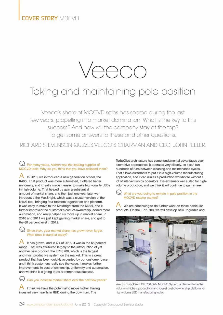
Veeco’s TurboDisc EPIK 700 GaN MOCVD System is claimed to be the industry’s highest productivity and lowest cost-of-ownership platform for high-volume LED manufacturing today.
Veeco v6RS.indd 24 29/05/2015 12:27
Copyright Compound Semiconductor June 2015 www.compoundsemiconductor.net 25
COVER STORY MOCVD
enhancements to the product that will take it to even higher levels of performance in the future. One of the things that our customers have come to know us for is introducing a product and then really staying with the product to provide additional features and enhancements that can make it better over time.
Q Shipments of MOCVD tools are very volatile. How can you run a business where shipments of tools may have to double in a few quarters, and then pull back just as hard afterwards?
A We work with a couple of different outsourcing manufacturing partners that we have worked with for many, many years. They can bring additional people to our product line when needed.
It is really important that we have a lot of variable costs and not too much fixed cost in our manufacturing. When you have a lot of fixed cost, you carry all this overhead and the down cycles just destroy you. We do this in manufacturing and some other areas of the company where we will use contractors, and variable labour that we can ramp up or down.
Q What are the factors that matter to customers? Is it all about reducing chip costs, or do they still need to improve the uniformity and the quality of their epiwafers?
A It is really all of those. Customers are looking for better epitaxial performance; better uniformity wafer-to-wafer, as well as within the wafer; they are looking for run-to-run repeatability,
and really excellent uniformity and tight binning; and all of that in a very economical manner.
Our customers are in a very competitive environment, and our goal is to give them a tool that can lower their cost of making very-high-quality LEDs, and in essence give them a competitive advantage in the market place. That approach from us has really paid off for our customers.
We have also designed our system so that it is very easy for customers to change wafer sizes, and as the industry moves up from 2-inch to 4-inch to 6-inch, that’s very easy to do and does not require any hardware retrofits. That’s been a big success for both us and our customers.
Q There is overcapacity in the LED market, but chipmakers are still buying your tools. What are the compelling reasons for making these purchases?
A Well actually, the capacity levels are pretty high. In most of the regions, they are either in the upper 80 percent utilization, or even into the 90 percent. Those are typically levels where LED manufacturers start to order more tools, especially when the lead times are the normal five-to-six month levels.
We are seeing orders from most regions of the world. We have orders for new products from China and Taiwan and other regions, because of the compelling advantage of the products − as well as the continuing increase in LED demand for lighting. LED makers are bringing on new, larger tools to be able to keep
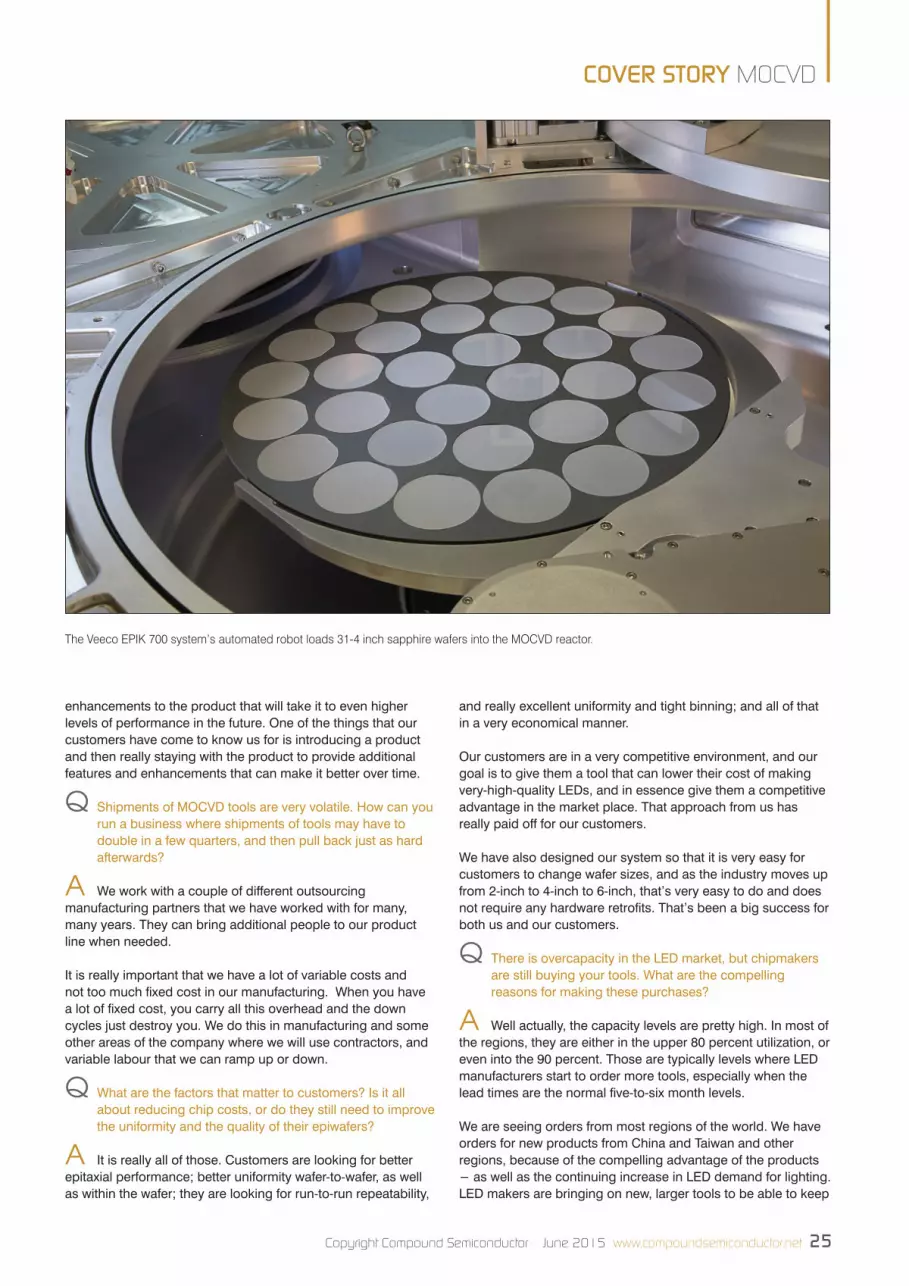
The Veeco EPIK 700 system’s automated robot loads 31-4 inch sapphire wafers into the MOCVD reactor.
Veeco v6RS.indd 25 29/05/2015 12:27
26 www.compoundsemiconductor.net June 2015 Copyright Compound Semiconductor
COVER STORY MOCVD
up with the demand over the coming years. They need to allow for a lead-time and a little bit of time for installation, and they want to make sure that they don’t lose market share.
Q You recently launched the EPIK 700. How does that compare to the K465i and the MaxBright tools?
A The EPIK 700 is the industry’s highest productivity and lowest cost-of-ownership MOCVD production system today. It includes two chambers, each twice the size of previous generations. It gives a 20 percent cost-per-wafer reduction, exceptional uniformity and repeatability, a high level of automation, and it maintains the very long run campaigns that our products have been known for. It also has about twice the footprint efficiency, so if you are looking to bring more capacity into your fab, you can bring in a lot of capacity without tying up too much room.
Q What do you believe can set an LED chipmaker apart from the crowd? Is it superior IP, better engineers and recipes or more capable growth tools?
A To be successful, they have to have exceptional engineers and have developed very good recipes for making LEDs that have high brightness and good characteristics, in order to be able to cost-effectively compete. If you combine the design and the IP with superior tools and an effective organisation to do the back-end processing, you have a real recipe for success.
Q A lot of your success has come from China. Why have you been able to do so well in that market?
A Well, we focused on making tools that were high-throughput, relatively easy to use, very reliable, very
dependable, and suited to high-volume mass production. China has brought on tremendous-sized fabs with many tools, and it is in a high-volume production mode. Our products are really superior in that case.
I would add that we have also built a very strong service and support infrastructure in China. We saw it as a strategic region and we actually moved very early in the 2010 up-cycle to build a training facility there. We have trained tremendous numbers of staff in China on how to use our products effectively, and how to help our customers get a lot of benefit out of the products.
Q It looks like China could dominate LED chipmaking by the end of this decade. Is that what you are expecting?
A They are certainly making large investments, and the Chinese government continues to offer subsidies to the top LED companies in China. They are building tremendous capacity to make high-quality LEDs. There was a time, four or five years ago, where some people predicted that wouldn’t happen. But it has happened, and they will be the industry leader.
Q Why has China failed to produce its own MOCVD toolmaker that can rival the leading players in this field?
A MOCVD tools are very complex. To do a really good job you need to understand the process for making LEDs and have deep background knowledge. In our case, we have decades of experience in this area, and we have funded tremendous levels of R&D every year for many, many years. So we have stayed ahead.
It’s been very, very difficult for outsiders to break into this market. Aside from the Chinese toolmakers not being successful, it was also true of other US companies, as they tried to break into this market back in 2009 and 2010. They couldn’t do it.
Q Not all MOCVD reactors are used to make LEDs. Some are used to make power electronic devices. Do you expect shipments in this sector to soon be a significant proportion of your MOCVD sales?
Veeco’s EPIK 700 IsoFlange technology within the reactor provides a homogeneous laminar flow across the entire wafer. This improves wavelength uniformity, and drives higher yields in a tighter bin.
The recently launched Veeco Propel PowerGaN MOCVD system enables the development of highly-efficient GaN-based power electronic devices.
Veeco v6RS.indd 26 29/05/2015 12:27
Copyright Compound Semiconductor June 2015 www.compoundsemiconductor.net 27
COVER STORY MOCVD
A We’ve been selling tools in R&D applications for GaN power electronics for a number of years. Our customers gave us feedback that they needed better ability to make very-high-quality films with very high levels of uniformity, and in order to address that, we designed a unit specifically for that market. It is a single-wafer reactor, which enables it to have really superior performance in terms of film characteristics and uniformity, and since it also has the TurboDisc technology, it produces wafers with very few defects.
About six months ago we started to sell that product, the Propel PowerGaN MOCVD system, to enable the development of highly efficient GaN-based power electronic devices. Customers are using it in R&D and pilot lines to perfect their recipes.
We named it Propel because we think it is going to help to propel this market to the inflection point. I think it is going to take a couple more years where the market is nearing an inflection, and two or three years from now I think it will be a very significant part of our revenue stream. We are sowing the seeds now, and the reception from customers has been outstanding.
Q There is the possibility that III-Vs could be used for making the channels of next-generation transistors for microprocessors. Are you preparing for that?
A We are. It is an opportunity that we are investigating and evaluating, and doing early research. We have worked with
some of the industry leaders in this area, and we will continue to prepare. We think it is way out on the roadmap, and as we get closer we will have the right platforms to address the technology.
Q For many years, makers and developers of multi-junction cells have hoped that the concentrating photovoltaic market might take off. Do you see an opportunity there?
A We continue to sell MOCVD systems into those multi-junction markets. Our systems have a real throughput advantage in those applications. We sell some units every year, and we see some new potential there.
It always comes down to whether someone can make the economics work and get a system that can be widely deployed and have an attractive cost-per-Watt. We are selling into that market, and we hope that it will hit the inflection point with the right company.
The single-wafer reactor of the Propel PowerGaN MOCVD system delivers high quality films with very high uniformity for the GaN-based power market.
Since joining Veeco in 2007, Chairman and CEO John Peeler has led the transformation of the company into a high growth, technology leader in LED, Solar and Data Storage Process Equipment markets.
Veeco v6RS.indd 27 29/05/2015 12:27
28 www.compoundsemiconductor.net June 2015 Copyright Compound Semiconductor
INDUSTRY SHARES
Compound semiconductor shares:
The good the badthe ugly
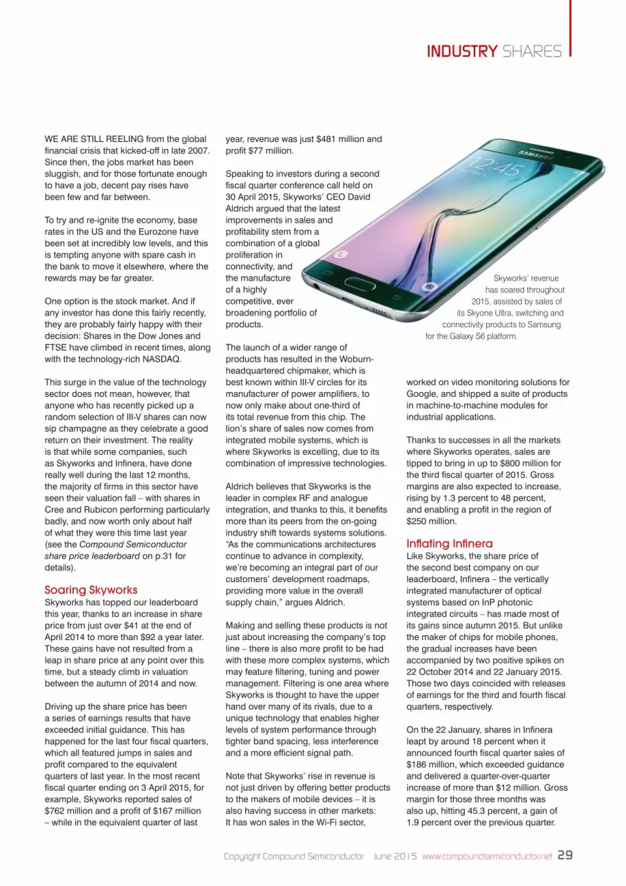
The last 12 months have produced mixed results for compound semiconductor shares: While those in Skyworks have soared, most have
headed south, with those for Rubicon falling through the floor
RICHARD STEVENSON REPORTS
Shares v2RS.indd 28 29/05/2015 12:29
Copyright Compound Semiconductor June 2015 www.compoundsemiconductor.net 29
INDUSTRY SHARES
WE ARE STILL REELING from the global financial crisis that kicked-off in late 2007. Since then, the jobs market has been sluggish, and for those fortunate enough to have a job, decent pay rises have been few and far between.
To try and re-ignite the economy, base rates in the US and the Eurozone have been set at incredibly low levels, and this is tempting anyone with spare cash in the bank to move it elsewhere, where the rewards may be far greater.
One option is the stock market. And if any investor has done this fairly recently, they are probably fairly happy with their decision: Shares in the Dow Jones and FTSE have climbed in recent times, along with the technology-rich NASDAQ.
This surge in the value of the technology sector does not mean, however, that anyone who has recently picked up a random selection of III-V shares can now sip champagne as they celebrate a good return on their investment. The reality is that while some companies, such as Skyworks and Infinera, have done really well during the last 12 months, the majority of firms in this sector have seen their valuation fall – with shares in Cree and Rubicon performing particularly badly, and now worth only about half of what they were this time last year (see the Compound Semiconductor share price leaderboard on p.31 for details).
Soaring SkyworksSkyworks has topped our leaderboard this year, thanks to an increase in share price from just over $41 at the end of April 2014 to more than $92 a year later. These gains have not resulted from a leap in share price at any point over this time, but a steady climb in valuation between the autumn of 2014 and now.
Driving up the share price has been a series of earnings results that have exceeded initial guidance. This has happened for the last four fiscal quarters, which all featured jumps in sales and profit compared to the equivalent quarters of last year. In the most recent fiscal quarter ending on 3 April 2015, for example, Skyworks reported sales of $762 million and a profit of $167 million – while in the equivalent quarter of last
year, revenue was just $481 million and profit $77 million.
Speaking to investors during a second fiscal quarter conference call held on 30 April 2015, Skyworks’ CEO David Aldrich argued that the latest improvements in sales and profitability stem from a combination of a global proliferation in connectivity, and the manufacture of a highly competitive, ever broadening portfolio of products.
The launch of a wider range of products has resulted in the Woburn-headquartered chipmaker, which is best known within III-V circles for its manufacturer of power amplifiers, to now only make about one-third of its total revenue from this chip. The lion’s share of sales now comes from integrated mobile systems, which is where Skyworks is excelling, due to its combination of impressive technologies.
Aldrich believes that Skyworks is the leader in complex RF and analogue integration, and thanks to this, it benefits more than its peers from the on-going industry shift towards systems solutions. “As the communications architectures continue to advance in complexity, we’re becoming an integral part of our customers’ development roadmaps, providing more value in the overall supply chain,” argues Aldrich.
Making and selling these products is not just about increasing the company’s top line – there is also more profit to be had with these more complex systems, which may feature filtering, tuning and power management. Filtering is one area where Skyworks is thought to have the upper hand over many of its rivals, due to a unique technology that enables higher levels of system performance through tighter band spacing, less interference and a more efficient signal path.
Note that Skyworks’ rise in revenue is not just driven by offering better products to the makers of mobile devices – it is also having success in other markets: It has won sales in the Wi-Fi sector,
worked on video monitoring solutions for Google, and shipped a suite of products in machine-to-machine modules for industrial applications.
Thanks to successes in all the markets where Skyworks operates, sales are tipped to bring in up to $800 million for the third fiscal quarter of 2015. Gross margins are also expected to increase, rising by 1.3 percent to 48 percent, and enabling a profit in the region of $250 million.
Inflating InfineraLike Skyworks, the share price of the second best company on our leaderboard, Infinera – the vertically integrated manufacturer of optical systems based on InP photonic integrated circuits – has made most of its gains since autumn 2015. But unlike the maker of chips for mobile phones, the gradual increases have been accompanied by two positive spikes on 22 October 2014 and 22 January 2015. Those two days coincided with releases of earnings for the third and fourth fiscal quarters, respectively.
On the 22 January, shares in Infinera leapt by around 18 percent when it announced fourth fiscal quarter sales of $186 million, which exceeded guidance and delivered a quarter-over-quarter increase of more than $12 million. Gross margin for those three months was also up, hitting 45.3 percent, a gain of 1.9 percent over the previous quarter.
Skyworks’ revenue has soared throughout
2015, assisted by sales of its Skyone Ultra, switching and
connectivity products to Samsung for the Galaxy S6 platform.
Shares v2RS.indd 29 29/05/2015 12:29
30 www.compoundsemiconductor.net June 2015 Copyright Compound Semiconductor
INDUSTRY SHARES
Speaking to investors at that time, Infinera’s CEO, Thomas Fallon, described the results for the fiscal year as outstanding: “Our 23 percent year-over-year growth, as compared to Dell’Oro estimates growth of 11 percent, marks the second consecutive year we have growth at least twice as fast as the overall market.”
Infinera’s success has continued into the first fiscal quarter of 2015, ending on 28 March. In a conference call on 21 April, Fallon claimed that in a typically a soft quarter for the industry, Infinera excelled because of its strength in many segments. Sales for the most recent quarter were $187 million, up 31 percent compared to the equivalent quarter of the previous year, and gross margin had climbed again, rising to 47.8 percent.
According to Fallon, part of this success comes from Internet content providers investing in their infrastructure. One example of this is Facebook’s recent deployment of an Infinera Transport Network that is lighting up the world’s longest terrestrial optical network route capable of delivering up to 8 Tb/s of data transmission capacity.
Other drivers behind Infinera’s increase in sales are a “robust demand” for its DTN-X platform that is used by tier-1, wholesale and enterprise carriers, and a significant rise in the capacity of the installed base of 100 Gig networks built over the last few years. In addition to this, the company’s Cloud Xpress platform that is designed for
the metro cloud is gaining traction, with contributions to first quarter sales coming from 10 GigE and 40 GigE versions of the product.
Further growth of the company will be propelled by the acquisition of Transmode, which is expected to be completed this autumn and will double the total available market for Infinera.
Fallon has high hopes for the marriage between the two most profitable companies in the industry:“Transmode is primarily positioned in Europe and delivering services-rich metro applications and Infinera primarily positioned in North America in delivering broad optical technology leadership.”
Before the merger takes place, Infinera is expected to announce the results of another strong quarter. Sales for the second fiscal quarter of 2015 should be in the range $195 million to $205
million, while gross margin is predicted to be around 46 percent.
An increase for IPGThird on the share price leaderboard is IPG Photonics, a vertically integrated manufacturer of fibre lasers. During 2014, shares of this company hovered at around $70, but they have steadily climbed this year, and were just below $90 at the end of April.
This gain in valuation will have been spurred by the very positive results for the recent quarters. Sales for the fourth fiscal quarter of 2014, ending on December 31, were $207.4 million, up 25 percent compared to the equivalent period of the previous year, while a gross margin of 55 percent contributed to a profit of $56.4 million. More recently, the company reported sales for the quarter that ended on 31 March 2015 of $199 million, along with a gross margin of 54 percent and a profit of $57.4 million.
Commenting on the latest results, company CEO Valentin Gapontsev claimed that IPG had made a terrific start to the year. “Despite foreign currency headwinds that impacted our anticipated sales growth, demand for IPG’s high-power fibre lasers boosted revenue 17 percent year-over-year for the first quarter of 2015.” And if the exchange rate had been equal to that of last year, sales growth would have been even better, topping 20 percent.
One of the markets that IPG serves with its fibre lasers is materials processing, and sales to this sector grew 18 percent compared to the equivalent quarter of 2014, due to increasing demand for products for cutting, welding and additive manufacturing.
Commenting on this, Gapontsev remarked: “We remain focused on gaining share in our established materials processing applications, developing new product applications that will expand our available market, and applying our lasers in large scale and novel applications beyond our core applications in materials processing.” These efforts are expected to deliver sales for the next fiscal quarter of between $215 million and $225 million.
Can Rubicon rally?Investors in the sapphire substrate manufacturer Rubicon, which is propping up the leaderboard, have had a hard time of late – shares have fallen to below $4, a price not seen since the darks days of the end of 2009. In early May 2014 the price tumbled from around $10 to $8, and after hovering at that mark until August, it nosedived to $6, and has subsequently undergone a steady decline.
The drop in share price last May could not be blamed on the reported sales on the first of that month, as revenue was up $2.8 million compared to the previous quarter, hitting $14.3 million. However, investors might have been concerned with the high wafer costs resulting from the introduction of patterned sapphire, which contributed to a loss of $10.9 million.
Three months down the line the share price dropped again, despite a slight increase in sales to $14.5 million. Concerns from investors may have been associated with high wafer costs, which were due to the large number of
Infinera says that it is experiencing robust demand for its DTN-X platform that is used by tier-1, wholesale and enterprise carriers.
Shares v2RS.indd 30 29/05/2015 12:29
Copyright Compound Semiconductor June 2015 www.compoundsemiconductor.net 31
INDUSTRY SHARES
patterned sapphire samples produced and the cost of establishing a 4-inch polishing line.
Establishing this line, and the company’s development of large wafers sizes, should bode well for the future. Commenting on this last August, the CEO of the time, Raja Parvez, remarked: “Now that MOCVD utilization rates are high, many LED chip manufacturers are looking for ways to increase throughput from existing operations, and moving to a larger substrate is one of the most effective ways to do that. We view the recent move to four-inch substrates as validation of our belief that we will soon see greater adoption of 6-inch and even 8-inch substrates.”
During that quarter, the company carried out its initial qualification of 4-inch and 6-inch patterned sapphire wafers at three customers, two of which are major, international LED chip manufacturers. The hope was that by 2015 these customers would be providing significant sales to Rubicon.
Fast-forward to the next earnings release on 12 February, and there was still little sign of better times ahead. On that day, sales of only $8.9 million were reported for the final fiscal quarter of 2014, with the new CEO – former chief financial officer William Weissman – describing the sapphire market as challenging, with continued pricing pressure and fluctuations in demand: “We expect to sell higher volumes and to begin driving down product costs in the first quarter, but price reductions will minimize the
impact. As a result, we expect first quarter 2015 results to be similar to the previous quarter.”
Just before this issue of Compound Semiconductor went to press, Rubicon announced its latest set of results: revenue of $8.9 million and loss for the quarter of $ 8.3 million. The impact to the share price has been a rise/fall of 6 percent.
Rubicon clearly has a long, hard road to climb to establish profitability, and it could easily be caught up in a storm created by pricing pressures and inventory levels. However, this materials supplier appears to be adopting a sensible strategy, by making an effort to distinguish itself from its rivals by developing patterned sapphire. It is an approach that will allow Rubicon to become more vertically integrated – which is a hallmark of the three most successful companies of the last year: Skyworks is no longer just a maker of power amplifiers, but builds front-end systems to simplify the task facing the makers of handsets; Infinera has always built InP circuits for its own systems, an approach that reduces the impact of overall margins on chip costs and yields; and in a similar vein, the chips from IPG go into its own fibre lasers.
Whether it is essential for chipmakers to seek some form of vertical integration to deliver high levels of profitability and a rising share price is not yet clear, but it will be interesting if these characteristics are seen in those companies that will top the share price leaderboard in 2016.
“Whether it is essential for chipmakers to
seek some form of vertical integration to deliver high levels of
profitability and a rising share price is not yet clear, but it will be interesting
if these characteristics are seen in those companies that
will top the share price leaderboard in 2016
”
Shares v2RS.indd 31 29/05/2015 12:29
32 www.compoundsemiconductor.net June 2015 Copyright Compound Semiconductor
INDUSTRY LEDs
AFTER DOMINATING high-power lighting for decades, the incandescent bulb is losing ground to the LED. This alternative is making inroads in automotive lighting, warehouse and bay lighting, and being used as an industrial ultraviolet light source.
But there is a big problem with this solid-state source: As it moves further into the high power arena, the age-old issue of heat dissipation is rearing its head. Despite the enormous efficiency advantage of the LED over an incandescent source, more than two-thirds of the electrical energy is still wasted as heat, and if this is not removed it can cause catastrophic failure within the chip.
Although the proportion of energy lost as heat is higher in the incandescent source, dealing with it is actually easier. That’s because the vast majority of the heat produced by this class of bulb is in the form of infrared radiation, which can dissipate into the air beside the glass enclosure. In contrast, the primary route for extracting heat from the packaged LED is conduction.
To conduct heat away as quickly as possible, LEDs are placed in contact with highly thermally conductive materials such as AlN. And further benefits in heat dissipation can be wrought
with additional thermal management substrates, heat pipes and active or passive heat sinks.
Whatever approach is taken, however, the thermal path is only as good as its weakest point. And if the interface between the LED and the heat sink, or any other part, fails to conduct heat sufficiently well, the LED die will reach unacceptable temperatures. This will adversely affect the LED; shortening its lifespan, decreasing the light output, degrading the quality of light and ultimately causing device failure.
Aluminium-based compoundsThe LED industry’s most common approach to thermal management is to mount the high-power chip on an AlN-based ceramic. This platform excels in two regards, combining superb thermal conductivity with good electrical insulation. The latter of these qualities is essential, because high-power LEDs often comprise a cluster of much smaller parts joined together by electrical connections.
Unfortunately, while AIN is more than up to the task of dispersing heat from a high-power LED, it has one huge drawback – it is extremely expensive.
Don’t bank on this situation changing,
because ceramic AlN is synthesized using exotic manufacturing techniques, such as the carbonthermal reduction of aluminium oxide and the direct nitridation of aluminium. Very few companies have the facilities required to produce AIN by these methods, hampering competition in the marketplace, while the innate brittleness of this ceramic leads to relatively low yields. To prevent breaking, the AIN ceramic packaging substrates tend to be supplied in square panels with sides that are 4-inch in length. Panels this small limit the number of LEDs built on a single tile and hamper attempts to realise economies of scale.
It can be argued that the high cost of AlN and its unsuitability for volume manufacturing is having a negative impact on the LED market, driving up the cost of packaged chips used in high-power arrays of devices. This has spurred designers to cast around for alternatives that sport the thermal conduction capabilities and good electrical isolation of AIN, but are cheaper and available in a form that permits integration into a high-volume LED production line.
An obvious candidate is aluminium, an excellent conductor of heat. This metal is cheap and available in an almost unlimited variety of shapes and sizes. However, attempts to anodize the
Keeping cool
with nanoceramics
Makers of solid-state lighting should turn to aluminium nanoceramics to cut the cost of thermal management in high-power LEDs
BY RALPH WEIR FROM CAMBRIDGE NANOTHERM
Nanotherm_v6RS.indd 32 29/05/2015 12:31
Copyright Compound Semiconductor June 2015 www.compoundsemiconductor.net 33
INDUSTRY LEDs
surface of aluminium and create a dielectric layer between the LED die and the thermally conducting material (the aluminium itself), while trying to retain most of the thermal conductivity of the aluminium, have been an abject failure. Anodizing is incapable of producing a surface that is reliable and sufficiently uniform to act as a dielectric, and instead this treatment creates voids and fissures. These imperfections expose the aluminium beneath to electrical currents from above, creating a short circuit.
However, despite all these shortcomings, it would still be imprudent to dismiss aluminium. After all, this metal has many merits: it is cost-effective, readily available, lightweight and flexible. What’s more, there are a wide range of suppliers of thermal management solutions
using aluminium as a core part of their business, massively increasing the potential supply chain. All that is needed is to uncover a compatible dielectric coating. At Cambridge Nanotherm of Haverhill, UK, we have found a way to create such a coating – we employ a
A packaged LED mounted on a Metal Clad PCB starboard
Nanotherm_v6RS.indd 33 29/05/2015 12:31
34 www.compoundsemiconductor.net June 2015 Copyright Compound Semiconductor
INDUSTRY LEDs
patented electrochemical process that transforms the surface of an aluminium sheet into a dielectric nanoceramic layer of crystalline aluminium oxide.
One of the great strengths of this approach is that the aluminium oxide – in the form of crystals that are bonded to the aluminium at the atomic level – ensures a clear ‘thermal path’. That is, the interface resistance between the alumina and the aluminium is small.
The size of these alumina crystals is on the nanoscale, with dimensions down to 30 nm. This permits the dielectric layer to be orders-of-magnitude thinner than anything else available. Consequently, heat has very little distance to go when travelling through the ceramic layer to the highly conductive aluminium beneath.
An example of a Nanotherm DM Metal Clad PCB
An additional advantage resulting from the tiny size of the crystals, and the process by which they are created, is that the dielectric layer is incredibly uniform, with no weak spots. Thus the dielectric remains intact, even when it is grown on thin sheets of aluminium that have to flex or bow during subsequent processing or in service.
The nanoceramic-aluminium composite produces a thermal conductivity of 152 W/mK, which is very close to that of just aluminium. Thermal conductivity of the nanoceramic layer alone is around 7.2 W/mK, an extremely high value by industry standards. Meanwhile the dielectric strength is a highly impressive 50 μV/m.
Note that the thickness of this
nanoceramic layer can be tightly controlled, making it possible to tailor the dielectric of the thermal substrate to a particular product’s breakdown voltage requirements. Another attribute of this nanoceramic is that it can endure extensive thermal cycling − from around -40 °C to around +250 °C − without degradation.
Origins and techniqueOur approach to making an aluminium oxide film stems from research dating back to the 1980s by our twoco-founders, Pavel Shashkov and Sergey Usov, former researchers at the Moscow State University. This duo first focused on creating crystalline structures on the microscale. However, the unique properties of ceramic AlN only became apparent with the discovery that the manufacturing process could move into nanoscale.
The details of this process are closely guarded and ring-fenced by several patents. What can be revealed, however, is that the process involves ensuring extraordinarily precise control of the chemical aspects of the conversion process, and the application of energy required to power the conversion (which in itself pushes the limits of high-power electronics).
When LEDs are attached to a substrate to improve thermal management, a circuit must be added. To realise this, we have developed a technology known as Nanotherm DM (Direct Metallisation), which involves using thin-film techniques to atomically bond a copper track directly to the nanoceramic surface of the aluminium. Tracks of standard thickness, such as ‘one-ounce’ copper, are defined by electroplating.
This approach sets a new benchmark for circuit bonding. Thermal resistance
“An additional advantage resulting from the tiny size of the crystals, and the process by which they are created, is that the dielectric
layer is incredibly uniform, with no weak spots. Thus the dielectric remains intact, even when it is grown on thin sheets of aluminium that have to flex or bow during subsequent processing or in service
”Nanotherm_v6RS.indd 34 29/05/2015 12:31
Copyright Compound Semiconductor June 2015 www.compoundsemiconductor.net 35
INDUSTRY LEDs
Nanotherm’s process (top) forms an extremely dense layer of ceramic on the aluminium base, providing a reliable insulation. In contrast, anodising (bottom) forms a layer which is fractured – clearly not to be relied upon to prevent penetration of electrons through the dielectric layer.
can be as low as 0.02 K/W on a 1.5 mm board, while thermal conductivity between the top surface of the one-ounce copper track and a 0.6 mm aluminium alloy heat sink can hit 152 W/mK, according to the laser flash technique. This level of conductivity is in the same ballpark as metallised AIN.
Our technology also has the upper hand over the incumbent when it comes to the addition of vias in the thermal substrate beneath the die array. The vias provide electrical pathways between tracks on each side of the part, but in an AlN substrate they are expensive to fabricate and act as sites of mechanical weakness. Turn to our technology, however, and holes can be simply drilled through the aluminium before processing.
The nanoceramic coating then grows uniformly on the inside surfaces of the vias, providing electrical isolation, while the deposited copper provides electrical connections.
With the technical requirements taken care of, adoption comes down to cost – and it is here that aluminium nanoceramics win hands down. As a rule of thumb, aluminium nanoceramics are two-to-four times cheaper than AIN when they are implemented, in large panels, as a fully circuitized high-power LED packaging substrate. Note that this major cost saving is realised while exhibiting similar performance.
The cost saving is not surprising. It is partly because the approaches to producing an aluminium nanoceramic are far less exotic than that used for making ceramic AlN; and it is partly because the substrates can be far larger. Thanks to the robust physical properties of the aluminium and the ceramic layer, boards can be an order of magnitude larger than those for AlN, leading to significant economies of scale.
Commercial opportunitiesThe LED market for nanoceramics is extensive, and it can be split into two distinct categories. The LED submount market for device packaging is an early adopter of the material as a replacement for AlN. The other key LED market is that associated with clusters, arrays, modules and chip-on-board LEDs. All of these have traditionally used AIN or epoxy-coated-aluminium printed circuit boards.
Manufacturers that are turning to nanoceramic aluminium are enjoying significant cost savings without compromising the quality of their products. In fact, they are finding that performance goes up, with a switch to epoxy-coated aluminium substrates with nanoceramics driving a 23 percent hike in lumen output while maintaining the temperature – and thus the lifetime – of the module. This means a reduction in die count is possible for the same lumen rating – enabling significant cost savings to the total bill of materials.
Trimming costs is a big deal, because it can help the LED market address one of the key sticking points that is holding up the mass market acceptance – initial purchase price.
Since full scale production started in 2014 demand has soared. To address this, over the next 12 months we are expanding our current factory, based just outside Cambridge, by adding additional manufacturing capacity. We are also planning to add new factories overseas, bringing our nanoceramics closer to target markets such as the US and Asia. These factories will be able to take advantage of lower production costs, making the nanoceramic proposition even more compelling.
Material for the thermal management of LEDs should have a conductivity comparable to that of AlN, but be much cheaper. Cambridge Nanotherm’s technology combines high thermal conductivity with comparatively low cost.
Nanotherm_v6RS.indd 35 29/05/2015 12:31
36 www.compoundsemiconductor.net June 2015 Copyright Compound Semiconductor
TECHNOLOGY LASERS
Instant imaging with
terahertz lasersWafer-bonding can create powerful terahertz lasers for real-time imaging of hidden weapons, illicit drugs and forms of cancer
BY MARTIN BRANDSTETTER, CHRISTOPH DEUTSCH, MICHAEL KRALL AND KARL UNTERRAINER FROM VIENNA UNIVERSITY OF TECHNOLOGY
ONE OF THE MOST APPEALING superpowers held by science fiction heroes is X-ray vision. By seeing through physical matter and revealing hidden objects, they uncover what is believed to be held secret and are able to foil the plans of villains.
Back in the real world, X-ray vision is also valued, because it can aid security checks and provide quality control. But it suffers from a massive drawback: Due to high photon energies, radiation at X-ray wavelengths is ionizing and exposure to it
is harmful.
A possible alternative exists at the opposite end of the electromagnetic spectrum, towards the microwave region. In this spectral range, radiation is not ionizing, thanks to photon energies that are orders
of magnitude below those of X-rays. What’s more, microwaves can penetrate
Terahertz Imaging v6RS.indd 36 29/05/2015 12:32
Copyright Compound Semiconductor June 2015 www.compoundsemiconductor.net 37
TECHNOLOGY LASERS
materials that are opaque in the visible, so it can reveal the contents within containers, which is why this technology is already being used in security scanners at airports. However, although this technology is convenient for imaging large objects, and people as a whole, its resolution is limited by the wavelength of the source – and that is of the order of a millimetre.
Fortunately, it is possible to find a spectral range that offers the best of both worlds – that is, one that avoids nasty blasts of ionizing radiation, while producing images that are sharp enough to uncover all the necessary details. Such attributes are found in the terahertz region that lies between the microwave and mid-infrared. Here radiation is non-ionizing, so is not harmful to biological tissue, and it has a wavelength of the order of 100μm, enabling adequate imaging resolution. Many materials have unique absorption characteristics in this spectral range, making this source of radiation ideal for accurate determination of different substances.
Thanks to these strengths, it is easy to think of many tasks that could be carried out with terahertz
sources, including non-destructive material analysis, remote sensing and imaging. Such applications are not only interesting for scientific purposes − they also highly desirable for industry, biomedicine and security technology. And progress has already be made in this direction, with terahertz sources used today to detect cancers, identify illicit drugs and detect concealed weapons.
Holding back far greater deployment of terahertz imaging systems is the image acquisition time. Many techniques are based on a single detector element, which necessitates the scanning of an object. Depending on the desired resolution and the integration time, taking a single picture can take up to several minutes.
Fortunately, thanks to the rapid development of microbolometer cameras, recently it has become possible to perform real-time imaging. To do this,
a high power terahertz source must illuminate the object. There are several ways to do this, but by far the most elegant is to use a quantum cascade laser (QCL) with sufficient power. Our team at the Photonics Institute at the Vienna University of Technology has developed such a source, which incorporates a wafer-bonded active region to increase output power.
Terahertz technologiesFor many years, the lack of any practical source of radiation has held back deployment of terahertz imaging (see Figure 1 for an overview of the sources). The options below 1 THz are dominated by: electronic sources such as resonant tunnelling diodes; semiconductor amplifiers that involve the use of multiplier chains; and vacuum techniques, such as backward-wave oscillators. In all cases, the source of radiation becomes very inefficient when approaching higher frequencies.
For frequencies between 1 and 5 THz, the selection of available sources is even more
Terahertz Imaging v6RS.indd 37 29/05/2015 12:32
38 www.compoundsemiconductor.net June 2015 Copyright Compound Semiconductor
TECHNOLOGY LASERS
limited. Free electron lasers can emit huge terahertz powers, such as several kW, but they must be housed in large-scale facilities. Smaller options are the p-doped germanium laser, which can emit up to 10 W, but requires liquid helium cooling and a magnetic field – and the optically pumped terahertz laser, which can fit on a typical laser table. But every one of these classes of laser is impractical on account of its size, and this
is hampering the large-scale implementation of terahertz imaging.
Far smaller and more convenient is the QCL. First demonstrated in 2002, this tiny III-V chip can span 1.2 THz to 5.2 THz and deliver powers exceeding 1 W. But even it is far from perfect: At present, it cannot run at room temperature, with the maximum operation temperature limited to about 200 K, making cryogenic cooling essential. If liquid helium or liquid nitrogen is used for cooling, a bulky source results, so a Stirling cooler is preferred, which is based on the compression and expansion of a gas, similar to a conventional refrigerator, and is able to achieve temperatures as low as 40 K. With this form of cooling, the terahertz QCL is still a very efficient source of radiation between 1 THz and 5 THz (see Figure 1).
Producing more power To form QCLs, engineers must grow complex heterostructures featuring multiple coupled quantum wells that provide electron confinement in one direction. This form of bandgap engineering defines discrete energy levels − which translates into laser levels required for targeting a particular wavelength − and it governs carrier transport through the device. However, the active region is not the only major factor influencing the key characteristics of the laser, such as the output power, threshold current and maximum operation temperature. They are also dictated by the choice
Figure 1. Comparison of available sources of high power terahertz radiation. The left panel shows the achievable terahertz power for different frequencies. The right panel compares the efficiency of the respective sources in the region between 1 THz and 5 THz by means of how much of the input energy is converted into terahertz radiation. Terahertz quantum cascade lasers are very convenient sources in this frequency region with respect to the output power and the efficiency, even if cryogenic cooling is taken into account.
Figure 2. Illustration of a double-metal waveguide and the corresponding mode profile in the cross-section. The mode is squeezed into a sub-wavelength geometry, leading to an inefficient extraction of the optical power and a strongly divergent far-field. To couple the light out of the cavity more efficiently, a lens can be mounted on the laser facet, as shown in the right picture.
Terahertz Imaging v6RS.indd 38 29/05/2015 12:32
Copyright Compound Semiconductor June 2015 www.compoundsemiconductor.net 39
TECHNOLOGY LASERS
of waveguide. One common option, derived from microwave technology, is a microstrip waveguide (this may also be referred to as a parallel plate waveguide). Light is confined between a double-metal waveguide with sub-wavelength dimensions – it has a height of about 10 μm, while the emission wavelength is about ten times this.
This geometry has some pros and cons. The good news is that the facet reflectivity is very high due to the non-terminated microstrip line, thus the outcoupling losses are very low, allowing a high maximum operation temperature. But the downside is that the highly diffractive nature of the sub-wavelength aperture results in a poor far-field emission profile. To overcome this, the laser facet can be coupled to an antenna or to an optical lens (see Figure 2), enabling a ten-fold hike in extracted output power to more than 100 mW. Note that alternatives also exist for increasing the light extraction of double-metal waveguides, such as incorporating photonic crystals, metamaterials or distributed feedback structures into the laser. Another popular way for confining the light within the QCL is to sandwich the active region between a metal and a highly doped semiconductor plasmon layer. This combination leaks light into the substrate because the plasmon layer is partially transparent to the optical mode. A lower facet reflectivity results, boosting light out of the cavity (see Figure 3). But there is a price to pay for this: Reduced temperature performance, resulting from the low confinement of the optical mode within the active region.
Confinement within a QCL that sports a plasmon layer can be improved by simply increasing the height of the waveguide – a higher proportion of the laser mode is guided within the active region. Another benefit of this approach is the reduced interaction of the optical mode with the waveguide layers, thereby trimming the optical losses. And on top of these gains, more light is generated in the laser, thanks to an increase in the volume of the active region.
Turning to thicker waveguides is far from trivial, however. Heterostructures are grown by MBE, and the growth rates for this epitaxial technology are incompatible with thick structures.
An alternative approach, which we have pioneered, is to double the waveguide thickness by vertically stacking two individual active regions. This is accomplished with direct wafer bonding, a technique that avoids an interfacial adhesion layer. Instead, two semiconductor samples are literally fused together. This ensures excellent electrical and optical quality of the interface, and enables realisation of a successful device.
With our design, because one sample is bonded upside down on top of another, the active region must exhibit the same operation characteristics, in terms of threshold and gain spectrum, for both bias polarities (see Figure 4). To meet this requirement, we have developed a symmetric active region. In this structure, electron wavefunctions and thus operation characteristics are the same, regardless of the applied bias polarity (see Figure 5 for the bandstructure).
By stacking two active regions of this kind, pulsed output powers from a single facet have been propelled to almost 0.5 W. This is nearly four times the output of a device with single active region thickness. Our device is a very promising source for real time terahertz imaging. It could
Figure 3. Illustration of a semi-insulating surface plasmon waveguide and the corresponding mode profile. The mode penetrates into the substrate and is thus not confined at a sub-wavelength scale, avoiding some disadvantages of double-metal waveguides.
Figure 4. Illustration of the wafer bonding process. One active region is bonded upside down on top of the first one. Electrons are moving in the growth direction in one sample, and against it in the other one. Thus, the active regions need to operate the same way for both bias polarities. On the right, a scanning electron microscope picture of the cleaved laser facet of the device is shown.
Terahertz Imaging v6RS.indd 39 29/05/2015 12:32
40 www.compoundsemiconductor.net June 2015 Copyright Compound Semiconductor
TECHNOLOGY LASERS
be paired with a focal plane array with individual pixel elements that are standard microbolometers, operated at room temperature. These elements are typically optimized for mid-infrared frequencies of around 10 μm, making them widely used for thermal imaging − but they are also sensitive to terahertz radiation, because the detection principle does not depend on the wavelength. This detector technology has come on in leaps and bounds in recent years, with device costs and system dimensions plummeting.
Another strength of our imaging system is that it does not require cooling with bulky cryogenic equipment. Instead, we use a compact Stirling cooler, which enables heat sink temperatures as low as 40 K. High thermal load powers of up to several Watts can be cooled, making this technique predestined for convenient operation
of terahertz QCLs. We have constructed a compact imaging system using a microbolometer camera, terahertz optics and our QCL, which is mounted on a Stirling cooler and operated in a vacuum chamber. This delivers real-time imaging (see the top panel of Figure 6, which depicts one frame of a recorded movie, which shows a razor blade partially covered in a security envelope).
Future objectivesDemonstration of real-time terahertz imaging represents great progress, but in order for this technology to be widely deployed, there is the need for additional advances in the performance of the QCL. Managing the temperature of this device with a Stirling cooler is certainly a more practical approach than having to use liquid helium or nitrogen, but further improvement would result from a raising of the maximum operating temperature of the laser. If it could be extended to 240K, this would allow a switch to thermoelectric coolers, and ultimately a reduction in the dimensions of the imaging system.
Additional gains would result from more powerful QCLs. Such sources would aid real-time imaging and open the door to illuminating larger objects over greater distances. A great deal of effort is already being directed at this, with researchers in this field evaluating different active region designs, considering alternative material systems and developing improved waveguides.
There are also opportunities on the detector side, related to improvements in microbolometer cameras. These could be optimised for terahertz radiation. Gains have recently been made here, including the development of resonant antenna-like elements that drastically improve the signal-to-noise ratio and reduce the level of power required to illuminate an object. Although further progress is needed before terahertz imaging systems can be launched onto the consumer market, at least it is already possible to build versions today that are compact and convenient.
Figure 5. For the wafer bonding technique, a symmetric active region is necessary, showing the same characteristics in both bias polarities (positive or negative). The laser threshold and the gain spectrum are (almost) the same, regardless of whether the electron flow is in or against growth direction. The right picture illustrates the calculated bandstructure of a symmetric active region. The red arrows illustrate the lasing transition and the green ones the extraction transisiton from the lower laser level.
Figure 6. Real-time terahertz imaging setup. The right panel depicts one frame of a recorded movie, showing a razor blade covered by a security envelope (top). For illustration, a photograph of the blade outside the envelope is shown (bottom).
Further readingB. S. Williams Nature Photonics 1 9 (2007)M. Brandstetter et. al. Optics express 20 21 (2012)C. Deutsch et. al. Applied Physics Letters 102 20 (2013)M. Brandstetter et. al. Applied Physics Letters 103 17 (2013)P. Dean et. al. Journal of Physics D: Applied Physics 47 37 (2014)
Terahertz Imaging v6RS.indd 40 29/05/2015 12:32
Copyright Compound Semiconductor June 2015 www.compoundsemiconductor.net 41
TECHNOLOGY LOGIC
50 YEARS AGO, writing in the trade magazine Electronics, a young engineer by the name of Gordon Moore predicted that with every passing year, the number of circuit components on an integrated chip would double. And history attests that not only was he right over the next decade, which was as far as he considered this projection to hold true – he was right through to today. This
GaN: The logical successor to silicon?
Stressor layers that crank up the speed of electrons are enabling a novel form of GaN-on-silicon transistor to offer a promising route
to maintaining the march of Moore’s law
BY SUBRAMANIAM ARULKUMARAN AND GEOK ING NG FROMNANYANG TECHNOLOGICAL UNIVERSITY, SINGAPORE
has meant that since 1965, when Moore penned his paper, the silicon industry has progressed from a chip by Fairchild featuring 64 components to Intel’s Broadwell range of microprocessors that have a mind-boggling 1.3 billion transistors.
The driver behind this astronomical rise in the component count per chip has been the shrinking
GaN Logic v7RS.indd 41 29/05/2015 12:33
42 www.compoundsemiconductor.net June 2015 Copyright Compound Semiconductor
TECHNOLOGY LOGIC
of the dimensions of the transistor. This allows more transistors to be packed onto a chip, and also leads to improvements in performance that are needed for practical reasons – for example, an acceptable power consumption for a transistor on a chip with 64 components is far less stringent than that on an IC sporting a billion transistors.
For many years, simply trimming the transistor’s dimensions while maintaining its design wrought the kind of performance gains that were required for the next-generation of IC. But recently this has not been the case, so additional changes have been required, which have managed to prevent leakage currents from escalating. These steps include replacing the SiO2 gate with that made from HfO2 and switching from a planar device to that with a protruding fin.
The silicon industry is now preparing itself for its most radical change ever: the introduction of channels made from higher mobility materials. III-Vs are the leading candidates for electron transport, while germanium is being tipped to speed up the holes. Even the world’s leading chipmaker, Intel, is arguing that new channel materials are needed, revealing at the International Solid-State Circuits Conference held February 2014 in San Francisco, that the limit for silicon is the 10 nm node. Beyond that there is a need to turn to high mobility materials to maintain the transistor’s current while it operates at the lower voltages needed to ensure a decrease in the power that this device consumes.
Figure 2. The position of the micro-photoluminescence peak produced by the InAlN/GaN nano-channel fin can uncover the stress within the structure. Spectra (a) with and (b) without SiN stress layer.
Figure 1 (a) The InAlN/GaN fin-HEMT is formed on a silicon substrate. (b) A cross-sectional, high-resolution transmission electron microscopy image (x-axis cut view) uncovers the different layers in the device, and electron dispersive X-ray analysis reveals the concentration of individual elements in a 176 nm fin. (c) A cross-sectional, high-resolution transmission electron microscopy image (y-axis cut view) of the device. (d) The T-shape gate has three different stress regions: the SiN/Au/Ni stress layers, the SiN/Au/Ni/SiN stress layers and the SiN/SiN stress layers.
GaN Logic v7RS.indd 42 29/05/2015 12:33
Copyright Compound Semiconductor June 2015 www.compoundsemiconductor.net 43
TECHNOLOGY LOGIC
Introducing III-Vs into the channel will not be easy, but some progress has already been made. At the European microelectronics research centre imec, engineers operating on a 300 mm silicon line have recently formed transistors with InGaAs channels that deliver an impressive level of performance. These developments are in line with the International Technology Roadmap for Semiconductors, which projects that the next generation of digital ICs will include high mobility finFETs that are formed on silicon wafers and feature channels made from III-Vs and germanium.
The researchers at imec, along with others working in this field, are investigating the ternary alloy InGaAs for high-mobility channels for the nFET. Results indicate that these devices are capable of operating at the lower voltages required for next-generation ICs, but the current delivered by them is not that encouraging.
One way to increase current by an order of magnitude, so it exceeds 4000 mA/mm, is to turn to a different type of transistor – a GaN HEMT. Formed on SiC substrates in a far larger form than that suitable for an IC, this type of device is already targeting high-frequency, high-power microwave and high-power switching applications, and by shrinking lateral and vertical dimensions, researchers have produced transistors with high currents that operate with an enhanced electron mobility. However, these transistors have several ailments, including a high gate leakage and a low ratio between the on and off currents. The upshot of these weaknesses is poor electrostatic gate control.
To address these weakness our team – made up of researchers from Nanyang Technological University, Singapore, Institute of Materials Research and Engineering, A*STAR (Agency of Science, Technology, and Research), Singapore
and the The Ohio State University, USA – has developed lattice-matched InAlN/GaN HEMTs that feature a nano-channel fin structure. These are formed on silicon substrates, the only platform that is being considered for next-generation ICs.
One of the features of these devices is their intentionally introduced stress, realised through the incorporation of three different stressor layers in the nano-channel. These changes significantly enhance transport properties, even at a low operating voltage, which is one of the essential requirements for low-voltage logic circuits. The current in these devices is more than twice that in InGaAs FinFETs, while the electron velocity is more than 30 percent higher.
Formation of these transistors begins with the growth of a lattice-mtached InAlN/AlN/GaN device structure on a silicon substrate by MOCVD. We confirmed the composition with high-resolution scanning transmission electron microscopy and energy dispersive X-ray analysis (see Figure 1).
The key to the very high current density in our InAlN/GaN transistors has been the incorporation of three stressor layers that enhance the saturation velocity in the fin. The first, a 120-nm-thick layer of
Figure 3. Micro-Raman spectrum (E2-High) of a InAlN/GaN nano-channel fin without a SiN stress layer.
Figure 4. (a) Current-voltage (b) and transfer characteristics of conventional InAlN/GaN HEMTs and three-dimensional triple T-gate InAlN/GaN nano-channel fin-HEMTs.
GaN Logic v7RS.indd 43 29/05/2015 12:33
44 www.compoundsemiconductor.net June 2015 Copyright Compound Semiconductor
TECHNOLOGY LOGIC
SiN, raps over the fins, while the second – the Ni/Au T-gate – provides additional localized stress to this fin, due to a combination of metal in the foot-print, and the pairing of SiN and metal at the head. A PECVD-grown, 120 nm-thick passivation layer of SiN that covers the entire structure provides the third contribution to stress.
According to micro-photoluminescence spectroscopy, the in-plane tensile stress that results from the triple stressor is 0.47±0.02 GPa (see Figure 2). A similar figure has been obtained by micro-Raman spectroscopy, a technique that suggests a tensile stress of 0.39±0.12 GPa (see Figure 3).
Electrical measurements on our novel fin-HEMTs verify the benefits of stress. At a drain-source voltage of 6 V, the maximum drain current is 3940 mA/mm, while the transconductance is a record breaking 1417 mS/mm (see Figure 4). Using a two-dimensional model, it is possible to extract an electron velocity of 6.0×107 cm/s, which is nearly 90 percent higher than that of the conventional In0.17Al0.83N/GaN HEMT (see Figure 5). We believe that this record-breaking velocity stems from variable stress along the nano-
channel, which produces significant variations in the conduction-band-edge. Such variations could create an electron launcher effect, leading to a quasi-ballistic transport across the channel, and thus resulting in a hike in electron velocity.
There is good reason to believe that our devices have excellent high-frequency characteristics. Our measurements on a conventional InAlN/GaN HEMT reveal a cut-off frequency (fT) of 70 GHz, a value that agrees with that from a simple equation linking electron velocity to effective gate length. In comparison, our nano-channel device exhibits a record-breaking fT of 560 GHz, after plugging in the record-breaking transconductance to a related equation. This is the highest fT for any GaN-based HEMT.
It would be good to back up these extracted values with direct measurements of fT. However, that’s not easy. It is tricky to determine the fT values using S-parameter measurements, due to the existence of large device parasitics.
The transistors formed on SiC using AlGaN/GaN technology are better than our devices in one regard, having a superior maximum drain current – it can be in excess of 4000 mA/mm. However, the transconductance for these rivals is only around 1000 mS/mm at a drain-source voltage of 3 V. What’s more, fabrication of such a high-performance device requires some very complicated processes, such as the formation of deep gates with dimensions below 20 nm, self-alignment processes that use a source-drain gap of 100 nm, and an expensive re-growth technology to suppress parasitic resistances. And compounding all of these issues, these conventional devices are hampered by short-channel effects.
In sharp contrast, our proposed device is easier
Figure 6. (a) Current-voltage characteristics of a three-dimensional, triple T-gate InAlN/GaN nano-channel fin-HEMT. (b) A comparison of the electrical characteristics of an InAlN/GaN fin-HEMT and a conventional HEMT at an operating voltage of 0.5 V. Note that the measured Q-factor (gm/SS) of the fin-HEMT is 7.9.
Figure 5. Extracted electron velocity for three-dimensional triple T-gate InAlN/GaN nano-channel fin-HEMTs.
GaN Logic v7RS.indd 44 29/05/2015 12:33
Copyright Compound Semiconductor June 2015 www.compoundsemiconductor.net 45
TECHNOLOGY LOGIC
Further reading
N. Waldron et. al. 2014 Symposia on VLSI Technology & Circuits, 9-12 Jun. 2014, Honolulu, Hawaii S. Arulkumaran et. al. Appl. Phys. Lett. 106 053502 (2015)S. Arulkumaran et. al. IEEE IEDM Tech. Digest 594 (2014)T.-W. Kim et. al. IEEE IEDM Tech. Dig. 425 (2013)K. Shinohara et. al. IEEE IEDM Tech. Dig. 617 (2012)B. Lu et. al. IEEE Electron Device Lett. 33 360 (2012)C. Yadav et. al. IEEE Electron Device Lett. 35 612 (2014)S. Arulkumaran et. al. IEEE Electron Device Lett. 35 992 (2014)
Table I. Benchmarking of InAlN/GaN nano-channel fin-HEMTs with conventional InAlN/GaN HEMTs
to make, while having the capability to deliver record performance. It can be fabricated using conventional electron-beam-lithography or stepper technologies, approaches that can form nano-channels and conventional sub-micron T-gates. What’s more, our devices are not produced by encroaching on the limit of what is possible, but employ T-shaped gates of 170 nm – far larger than the 70 nm to 80-nm I-shape gates on 88-nm fins used by other research groups.
One implication of this situation is that we should be able to deliver an increase in performance through a reduction in device dimensions, such as a smaller fin width and gate-length. To do this we will need to optimise the device layout and fine-tune the stress in the transistors with materials that have different dielectric constants.
Our device also delivers impressive performance at an operating voltage of 0.5 V, which is within the regime that will be used in next-generation microprocessors. At this voltage, the drive current is 1030 mA/mm, transconductance is 646 mS/mm, and the ratio of the on-current to the off-current is around 106. Compared to a conventional InAlN/GaN HEMT operating at the same voltage, our novel device has the upper-hand in many key areas, with the exception of transconductance (see Figure 6 and table 1). This weakness might be addressed, however, through scaling of the gate-length.
The extracted electron velocity in our nano-channel transistor is 2.6 x 107 cm/s, indicating
an fT of 245 GHz, and implying that our device is capable of high-speed operation at the low operating voltages that will be employed in tomorrow’s microprocessors. But before it is deployed there, we will need to develop an off-state device – so far, all we have made is a D-mode, normally on device.
To do this, we can use E/D (normally off/normally on) type logic switches. It is possible to make an E-mode fin-HEMT by trimming the width of the fin, indicating that it should be easy to integrate E-mode (normally-off) fin-HEMTs with D-mode cousins on a single chip. This will allow us to demonstrate low driving voltage E/D logic circuits that are based on our stress-engineered transistors, and ultimately showcase a very promising route for maintaining the march of Moore’s Law.
GaN Logic v7RS.indd 45 29/05/2015 12:34
46 www.compoundsemiconductor.net June 2015 Copyright Compound Semiconductor
INDUSTRY MOCVD
Refined reactors trim chip costs
Automated reactors that accommodate more wafers and in-situ cleaning drive down the cost of making wide bandgap devices for power electronics
BY CHRISTOPH GIESEN AND MICHAEL HEUKEN FROM AIXTRON
Neuland Aixtron v3RS.indd 46 29/05/2015 15:04
Copyright Compound Semiconductor June 2015 www.compoundsemiconductor.net 47
INDUSTRY MOCVD
EFFORTS TO TRIM carbon footprints and cut energy bills are underpinning interest in increasing the efficiency of electrical systems. One way to do this is to stop controlling the flow of current with silicon transistors and diodes, and instead employ higher-efficiency devices made from wide bandgap materials.
Designers of electrical systems are only going to embrace this new chip technology, however, if the total bill of materials is no higher when products are built with these superior components – and unfortunately, that’s often not the case today. But this weakness associated with GaN and SiC diodes and transistors is being addressed, with these wide bandgap devices becoming increasingly
competitive through efforts such as the Neuland project. Backed by €4.7 million of funding from the German Federal Ministry of Education and Research (BMBF), this project ran from 2011 to 2014 and involved Infineon Technologies, Aixtron, SiCrystal AG and SMA Solar Technology.
The Neuland project has taken a two-pronged approach to meeting its primary objective: the enhancement of SiC technology, with the aim of slashing costs via improvements in material quality, which ultimately spawn a hike in yield; and the development of a completely new power electronics technology that is based on high-blocking vooltage GaN layers, which are grown on 200 mm silicon, a comparatively low-cost, large-scale substrate. These differing approaches are united by the same goal – to construct prototype diodes and inverters that deliver virtually loss-free switching and are capable of handling blocking voltages up to 1500 V and currents up to 10 A.
At Aixtron of Aachen, Germany, our role within the Neuland project has been to develop an MOCVD technology for the industrial production of GaN-based HEMT epistructures for power electronic devices. We have succeeded in this endeavour, creating a multi-wafer reactor that combines industry-leading throughput with a very high ‘up-time’, thanks to in-situ cleaning and a high degree of automation.
Growing on siliconA lack of availability of large, low-cost native substrates dictates that the manufacture of GaN HEMTs will always involve the growth of epilayers on a foreign substrate. While sapphire substrates are widely used for making GaN LEDs, they are not suitable for power electronics, because they have a low thermal conductivity and can bend at the elevated temperatures used for growth. Note that even during pre-growth heating, 150 mm substrates can lift several millimetres off the edge of the reactor surface and even break.
Meanwhile SiC, while offering excellent thermal conductivity, is limited in size and very expensive. Consequently, it is an obvious choice to select silicon substrates for developing GaN HEMTs. This platform is mature, excellent in quality, available in diameters of up to 300 mm, and provides a thermal conductivity comparable to that of GaN.
However, despite all these attributes, silicon is not a perfect substrate. Instead, growth is very challenging, due to significant differences in the thermal expansion coefficients and lattice constants of the GaN-based layers and the silicon substrate. These differences are to blame for stresses within the material, which build-up during growth and can cause curvature of the wafers – and once they cease to have full contact with the susceptor, problems are compounded by an inhomogeneous temperature distribution. Making matters worse, these issues are magnified with increasing substrate diameter, and it is even possible for cracking to occur during wafer cooling.
Makers of GaN-on-silicon LEDs also face these issues, but at least they don’t have to contend with additional problems stemming from the high aluminium content in the AlGaN films. Increasing aluminium content in ternary and quaternary material introduces more stress into the material, and also increases pre-reactions between the aluminium and nitrogen sources. The parasitic reactions that result are highly undesirable: They impair process efficiency, and they also introduce inhomogeneous depletion profiles that cause variations in material composition across the substrate. And on top of this, they can be a source of particles within the reactor. However, we have shown that by addressing all of these issues, it is possible to produce the form of AlGaN-based HEMT being developed in the Neuland project.
To make these HEMTs competitive with silicon equivalents, manufacturing costs must be as low as possible. The epitaxial
LEFT: The reactor chamber of Aixtron’s Planetary system AIX G5+ that can be used for the growth of GaN on 200 mm silicon substrates.
Neuland Aixtron v3RS.indd 47 29/05/2015 15:04
48 www.compoundsemiconductor.net June 2015 Copyright Compound Semiconductor
INDUSTRY MOCVD
growth process accounts for a significant proportion of chip costs, and to trim this we have investigated increasing the capacity of multi-wafer reactors, and refining the growth process as silicon substrate diameter increases from 100 mm to 150 mm and then 200 mm.
Efforts in this direction included the development of a 56 by 2-inch Planetary Reactor, based on our 42 by 2-inch (or 11 x 100 mm) reactor. This can also house either 14 wafers with a diameter of 100 mm, eight 150 mm wafers or five 200 mm wafers. Due to a lack of availability of industry-standard, high-quality, 2-inch silicon-substrates, we started development of our HEMT growth process on 100 mm wafers, before moving on to 150 mm and then 200 mm wafers.
and reproducible deposition of ternary and quaternary materials. Thanks to these new inlets, the growth window for depositing high quality layers significantly expanded.
In addition to these refinements, the other major breakthrough that we have made involves optimisation of the materials inside the reactor. This change reduced particle generation and extended the maintenance-free operation of the system.
Underpinning all of these changes to the design of our reactor were simulations that offered an insight into the impact of the new design on the deposition process. If these changes were positive, optimized parts were manufactured, implemented in the existing system and qualified for the process.
We also developed an improved chemical model for the epitaxial growth of aluminium-based nitrides. This model considers parasitic gas phase processes that can occur in an MOCVD chamber, and it draws on an extensive experimental database that reveals how the chemical behaviour of AlGaN is influenced not only by general considerations, such as temperature and partial pressure of the sources, but by the reactor design and the epitaxial process. Armed with all this information, we were able to make quicker progress as we refined our reactor’s design.
Optimising temperature profilesUniform temperatures are critical to realising high-quality epiwafers. To excel in this regard, we simulated the influence of different reactor components on the temperature profile within the growth chamber. Following optimisation via simulations, components were designed, manufactured and subsequently tested in the laboratory. By optimising the satellite design, we could hit the target for temperature deviation, but the variation from satellite to satellite exceeded the specification. To meet this requirement, we then developed a technology allowing in-situ adjustment of temperature deviations, and this enabled us to realise a ± 1 °C specification over all satellites.
Using this improved temperature uniformity, we manufactured HEMTs with an optimized technology on 150 mm substrates. These epiwafers exhibit state-of-the-art properties, with sheet resistance and breakdown voltages, measured in both the vertical and horizontal directions, comparable to those of commercial wafers from smaller reactors.
These epiwafers are also a success when viewed from another perspective − the targets set in the Neuland project. The goal of a mobility of 1600 cm2/Vs for a HEMT structure with a sheet carrier concentration of 1x1013 cm-2 was not only realised on 100 mm substrates, as intended, but also on 150 mm cousins. We were also able to produce non-An epitaxial wafer manufactured with
5 x 200 mm AIX G5+ system.
Improvements to the hardware carried out during the Neuland project included optimisation of the susceptor, the exhaust collector (flow dynamics), the gas inlet (flow dynamics, uniformity, efficiency) and the ceiling (particles and temperature management). We also developed a new susceptor design for either eight 150 mm or five 200 mm wafers. This is compatible with automation, while guaranteeing an extremely uniform temperature distribution over large silicon substrates.
Part of this work involved the development of specific gas inlets for the 150 mm and 200 mm configurations to ensure extremely homogeneous
Run-to-run stability for mass production: Thickness uniformity for five full load runs using same HEMT recipe.
Neuland Aixtron v3RS.indd 48 29/05/2015 15:04
Copyright Compound Semiconductor June 2015 www.compoundsemiconductor.net 49
INDUSTRY MOCVD
passivated samples with an average electron mobility of 1700 cm2 V-1 s-1 at a carrier concentration of 1.2 x 1013 cm-2, as well as crack-free, 6 μm-thick, highly resistive (>105 Ohm/sq.) buffer structures. And by employing the combination of an optimised reactor, epitaxy process and buffer structure, we could produce 200 mm epiwafers with a bow below 50 μm. This makes them flat enough to be processed in silicon lines.
To ensure that the production cost of these epiwafers is as competitive as possible, we have also looked at issues relating to throughput, such as the time taken for maintenance and fault fixing. This has led to increased automation, which can improve manufacturing efficiency. In-situ cleaning is a fundamental requirement for effective automation, and we have worked on this during and after the Neuland project.
The pay-off from in-situ cleaning is far greater than just the opportunity for increased automation, however. By ensuring equal starting conditions for every growth run, there are the promises of greater reproducibility and increased yield. What’s more, in-situ cleaning can alleviate the need to change hardware between production runs, thereby reducing cycle times and eliminating potential operator errors. Spare-part costs should also fall, as well as the number of particles in the process.
The G5 seriesWe have used our findings from the Neuland project to enhance our G5 product family, especially the AIX G5+. This reactor, a Planetary system capable of housing five 200 mm wafers, was launched in July 2012 and it still setting the standard for the manufacture of power electronic devices based on GaN-on-silicon technology.
As well as this, the insights that we garnered during the Neuland project have enabled us to improve our G5 warm-wall system, which has been exclusively designed for SiC epitaxy. This reactor can process up to eight 150 mm SiC wafers, and combines the highest wafer throughput with the shortest cycle times and lowest cost of ownership.
Improvements to reactor design and
Aluminium concentration uniformity in the AlGaN barrier of a GaN-based HEMT structure formed on 200 mm silicon.
process improvement didn’t stop at the end of the Neuland project, but are on going, now being pursued as part of a project funded by the European Union called HiPoSwitch. This effort, which aims to deliver advances in GaN-based normally off high-power switching transistors for efficient power converters, includes an examination of the possibilities to upgrade the MOCVD production capacity and efficiency.
Through this and Neuland we have developed, in three steps, a full automated MOCVD tool that can accommodate five 200 mm wafers. The
first of these steps involved optimisation of the reactor chamber to optimise growth on 200 mm substrates, and this was followed by implementation and optimization of the pre-developed in-situ reactor cleaning process to cut maintenance time between growth runs. The latter step enabled fully automatized cassette-to-cassette wafer handling, leading to a superior growth tool that has been qualified for the HEMT process.
Thanks to these developments, this reactor and its sibling for SiC growth are currently the most advanced systems for the volume production of power devices.
A 200 mm GaN-on-silicon HEMT epiwafer.
Neuland Aixtron v3RS.indd 49 29/05/2015 15:05
50 www.compoundsemiconductor.net June 2015 Copyright Compound Semiconductor
TECHNOLOGY LEDs
Throwing away
LED e f f i c i e n c y
Are parasitic currents in p-type layers holding back the efficiency of many commercial LEDs?
BY GREG TOGTEMA FROM LAKEHEAD UNIVERSITY AND K. SCOTT BUTCHER FROM MEAGLOW
NITRIDE-BASED LEDs are getting evermore efficient, enabling them to win deployment in situations demanding brighter light sources. At the beginning of the twenty-first century they produced enough lumens-per-Watt to backlight the screens of handsets, and now, thanks to a hike in efficiency, they are at the heart of solid-state bulbs for automotive and room lighting.
The tremendous gains in efficiency are setting this source apart from its incandescent counterpart, which ruled the roost through the twentieth century. Now outlawed in several countries due to its low efficiency, the incandescent generates light from a coil of very thin wire that is heated to such temperatures that it glows and emits some light and a high proportion of infrared radiation.
While LEDs are far more efficient than incandescent sources, they still waste a substantial proportion of electrical energy in the form of heat that drives up the temperature of the chip. This temperature must be maintained below what is known as the thermal limit to prevent a shortening of device lifetime.
To improve the performance of the LED, engineers aim to increase the efficiency of the chip while it operates at temperatures below the thermal limit. There have already been several refinements to LED design to succeed in this endeavour: thermal management has been improved through superior device packaging architectures, such as the introduction of a flip-chip design; heating within the chip has been reduced with better GaN buffer layers, which trim
the density of lattice dislocations; and device efficiency has risen, thanks to improvements to the design of the active region, which increase the likelihood of radiative recombination between electrons and holes.
Such efforts at improving the performance of GaN LEDs have already borne much fruit, leading to a period of diminishing returns. For example, adding more wells to the active region traps more carriers, but every additional well provides a smaller and smaller increase in light emission.
It is a similar story when driving an LED close to maximum current density, with each additional milliamp providing a smaller increase in light output. This stems from a decline in the efficiency
Meaglow v4RS.indd 50 29/05/2015 12:37
Copyright Compound Semiconductor June 2015 www.compoundsemiconductor.net 51
TECHNOLOGY LEDs
of the nitride LED at higher current densities, which is a well-known problem referred to as droop.
Many researchers within industry and academia are trying to understand and address it, because droop-tolerant designs could increase the light emission and the efficiency of a chip.
Eliminating droop is challenging, with efforts held back by a lack of consensus over its cause. Many theories have been put forward, with some groups arguing that droop stems from non-radiative Auger recombination, while others are blaming undesired effects of indium incorporation or pointing the finger at carrier ‘spill over’ across the heterojunction barriers.
Some of these theories have more persuasive arguments than others, but whatever the correct mechanism maybe, it is far from easy to build a droop-busting device. If Auger is the cause, the solution is to construct a high quality heterostructure that prevents electrons from scattering to energy states away from the quantum well conduction band minima. Meanwhile, if indium incorporation is not good enough, the growth temperature must be lowered – and if the quantum well heterostructure need optimizing, this will require redesign and testing.
Solving droop and addressing it is clearly very important. But it is not the only weakness that is dragging down the efficiency of the LED. It is also suffering from the poor quality of p-type doping
in GaN, a little-known but important issue that has been discovered by our team from Lakehead University and Meaglow.
The role of p-type GaN Studies of droop will miss this, because they tend to focus on the electro-optical conversion efficiency, which dictates the amount of light that can be generated per milliamp of applied current. What we have found relates to the current drift characteristics, which at least partially dictate the temperature rise per milliamp.
This rise in temperature varies across the heterostructure. The top p-type GaN layer used in an LED stack is typically one-to-two orders of magnitude more resistive than its silicon-doped, n-type counterpart,
Meaglow v4RS.indd 51 29/05/2015 12:37
52 www.compoundsemiconductor.net June 2015 Copyright Compound Semiconductor
TECHNOLOGY LEDs
and this is where the greatest device heating occurs. But if the resistivity in this layer can be improved through the likes of better doping or a superior crystal structure, this could lead to a better LED.
There are many well-known limitations associated with p-type GaN that restrict LED performance. Firstly, carrier concentration – which determines both conductivity and luminosity – has an upper limit of around 1018 cm-3, due to self-compensation of the acceptor impurity. Secondly, the acceptor dopant, magnesium, must be thermally activated to remove the ill effects of hydrogen. But doing this can have its downsides, impacting the indium in the quantum wells and leading to a blue shift in emission.
On top of these issues, we have uncovered another problem. We have discovered that in a manufacturing environment, intentionally p-type material often has a carrier concentration that is not vastly higher than the residual background n-type concentration associated with oxygen impurities. Although hero measurements suggest
that it is possible to grow undoped GaN with a background electron concentration of 1014 cm-3, this is far from typical. Far more common is that the hole concentration has to battle with a background concentration of electron donors of up to 1017 cm-3, even when no intentional n-type dopant is used.
We have recently investigated the impact of this background electron concentration, scrutinising characteristics of three commercially obtained p-type GaN templates from three different manufacturers. Using Hall effect measurements, we analysed the current flow in p-type GaN, finding that it is actually the background electron drift current that dominates the p-type drift.
That’s not to say that the material did not have p-type characteristics – they are seen in luminescence spectra – but current flow was mainly due to n-type behaviour, with Hall measurements indicating that the material was n-type.
This shocking result led us to first check our equipment, using standard samples
such as p-type germanium. We also spent considerable time confirming the quality of our ohmic contacts, but we could find nothing untoward, leading us to conclude that the measurements on these templates are not flawed.
How can this be, though, as the p-type doping level is higher than the n-type background? It’s because the Hall measurements consider carrier currents, a product of the carrier density and the mobility − and the mobility of electrons in p-type GaN is much higher than that for holes. In other words, when it comes to carrier concentration, compared to holes, electrons punch above their weight.
Many makers of nitride-based LEDs will be oblivious to this issue because they don’t examine the electrical characteristics of their p-type GaN with Hall experiments, due to difficulties in interpreting the results on measurements involving an epistructure with many different layers. Instead, these device makers tend to use mercury probe capacitive-voltage (CV) profiling to check their materials’ net carrier concentration − but this only determines the net charge across a depletion region. Such measurements are not influenced by carrier mobility, nor are they sensitive to the effects of carrier drift. All they reveal is that there is a net concentration of holes, which satisfies the manufacturers of LEDs that are unaware of the true nature of their GaN films.
In fact, these chipmakers are probably oblivious to the true hole current in their p-type layers – we have received films quoted as being a high
P-type templates provided by three different commercial suppliers had a carrier concentration that shows the dominance of n-type behaviour.
“LED chipmakers should also be concerned about the parasitic minority carrier current uncovered by Hall effect measurements.
Even if their p-type GaN is p-type, they will have a parasitic current present in the GaN p-type top layer of their LED stack
”Meaglow v4RS.indd 52 29/05/2015 12:37
Copyright Compound Semiconductor June 2015 www.compoundsemiconductor.net 53
TECHNOLOGY LEDs
1017cm-3 of holes, but because of the high mobility of the electrons, the value given by Hall measurements is an electron concentration of about 1018 cm-3.
These findings indicate that the background oxygen levels influence material properties well before they impact net carrier concentration. This happens through the existence of a parasitic minority carrier current in the p-type GaN.
The good news is that it is possible to reduce background electron concentrations in undoped and p-type GaN by taking appropriate steps for MOCVD growth. These include reducing any discernable air leaks in the gas flow system; using purifiers for gas supplies and highly purified metal-organics; ensuring that water vapour formed from ammonia byproducts or metal-organics is properly purged from the system; and employing proper purging and a sufficiently long pre-growth baking regime, so that background oxygen carrying species, such as water, are eliminated prior to film growth. These are recommendations that many chipmakers are already well aware of, but their importance makes a difference at a much earlier stage than they probably realise.
Impacting LED performanceLED chipmakers should also be concerned about the parasitic minority carrier current uncovered by Hall effect measurements. Even if their p-type GaN is p-type, they will have a parasitic current present in the GaN p-type top layer of their LED stack. This means that in addition to the primary current in the p-type GaN that is associated with the transport of holes to the active region, there can be a significant minority carrier current of electrons heading towards the back ohmic contact of the p-GaN. The latter current makes no contribution to light emission, so impairs device efficiency.
In experimental labs the emphasis is on material quality rather than wafer throughput, so we expect low background levels of oxygen and minimal minority carrier currents −
this might even be the case when background oxygen levels are not monitored on a regular basis. But for high-volume chipmakers that are churning out as many devices as possible, the lack of a proper method for measuring background oxygen levels may mean that this problem can slip by undetected, with device efficiency suffering in silence.
What is needed is an approach for monitoring minority carrier currents in p-type GaN structures. This information cannot be extracted from CV measurements, while Hall measurements are rather cumbersome. However, it should be possible to monitor carrier diffusion lengths in an industrial setting using optical pulses. This approach could be complemented by secondary ion mass spectrometry, a destructive, time-consuming approach that offers a direct measurement of oxygen levels.
One consequence of our work is that it begs the question: How big a problem is poor p-type doping in nitride LEDs? Well, it could be huge, based on the
p-type templates that we have examined from three commercial suppliers. If LEDs were made that incorporated p-type material found in these templates, their LED efficiency would be compromised significantly. This is a wake-up call for the need to monitor the quality of p-type GaN.
One may also wonder if the parasitic minority carrier currents contribute to droop. It is not trivial to answer this, as it would require knowledge of the relative voltage dependence of the majority and minority currents, plus a modelling effort that accounts for barrier heights and other material and device characteristics.
Exploring this is surely a worthwhile endeavour − but one for someone else. Our aim, particularly at Meaglow, is to continue to look at producing indium-rich InGaN on p-type GaN. By studying templates of this material, we discovered some alarming issues relating to the nature of commercial films of this nitride. We now hope that by making others aware of this potential pitfall, LEDs will soon be free of this particular malady.
Yellow-orange InGaN test device. The probe to the left is on a high indium content n-type InGaN layer. The probe to the right is on the underlying p-type GaN template. The blue purple emission from the p-GaN probe is because of the slightly n-type surface oxide, one of several possible sources of n-type minority carriers.
Meaglow v4RS.indd 53 29/05/2015 12:37
SUBSTRATES & MATERIALS AWARD
Element SixGaN-on-Diamond Wafers
DEVICE DESIGN & PACKAGING AWARD
Cree, Inc C2M0025120D
R & D CHIP DEVELOPMENT AWARD
DARPA Terahertz Electronics program
INNOVATION AWARD
Veeco Instruments Inc TurboDisc EPIK700 GaN MOCVD System
METROLOGY, TEST & MEASUREMENT AWARD
KLA-Tencor Corporation Candela CS920
WINNERS ANNOUNCEDThe CS Industry Awards recognise success and development along the entire value chain of the compound semiconductor industry from research to completed device, focusing on the people,
processes and products that drive the industry forward. The CS Industry Awards remind us what is good about the industry - the people who drive it with their technical expertise and
customer orientated perspectives.
The winners are:
The winners were presented at the CS International Conference, Frankfurt, Germany, on March 11th 2015For more information: www.csawards.net
Awards Sponsor
CS Industry Awards April May 2015 210x297 Ad.indd 1 23/04/2015 09:46
Six key themes:Over 30 inspiring presentations£ Where should the laser go?£ Driving deployment of PICs in datacentres£ Increasing the capability of optical networks£ What’s the role of the foundry?£ Do we have the tools for designing, making, packaging and testing PICs?£ A question of material: InP, silicon, or something else?
Photonics Integrated Circuits ConferenceCreating and strengthening links between chipmakers and network builders
1 - 2 March 2016, Sheraton Brussels Airport Hotel, Belgium
Co-located with the 6th CS International Conference
www.picinternational.net
Sales of PICs are soaring, with their deployment helping to boost the capacity of networks and data centres. To aid this industry, we are strengthening the relationships between the makers and the users of these integrated circuits by launching PIC International, a global conference dedicated to this industry. Attendees at the inaugural PIC International
conference will hear industry-leading insiders delivering more than 30 presentations spanning six sectors. This will equip the delegates at this two-day conference with an up-to-date overview of the status of the PIC industry, and provide them with many opportunities to meet other key players within this community.
Early bird discountBook your place before 30 November 2015 and receive a e100 discount.
Cost effective: low operating costs and little maintenance
Space saving: small footprint
Safe: low gas inventory
Reliable: continous gas supply
Visit us at SEMICON West - Booth #2231 to nd out more information!
Untitled-2 1 28/05/2015 12:26
Copyright Compound Semiconductor June 2015 www.compoundsemiconductor.net 57
RESEARCH REVIEW
T. Oka et. al. Appl. Phys. Express 8 054101 (2015)
RESEARCHERS from Toyoda Gosei are claiming to have set a new benchmark for the performance of a vertical GaN MOSFET with a device that has an on-resistance of just 1.8 mΩ cm2.
Not only does this 1.2 kV device better the on-resistance of other vertical GaN MOSFETs, which have realised on-resistances as low as 2-3 mΩ cm2 – it also breaks new ground by delivering the blocking voltages and threshold voltages required for use in high-power automotive applications.
Threshold voltages of 3-5 V are preferred for this application, in order to prevent false operation caused by factors such as noise. The team’s vertical MOSFET meets this requirement, having a threshold voltage of 3.5 V, while the more common lateral GaN transistors can rarely meet this need.
Another weakness of lateral GaN transistors is that in order to deliver a high breakdown voltage they must have a substantial gate-drain spacing, and this drives up the size and cost of the device. In comparison, with vertical transistors, an increase in thickness of the drift region leads to a higher breakdown voltage, with chip size remaining the same.
Back in 2014, the Toyoda Gosei team claimed a record-breaking blocking voltage of 1.6 kV for a GaN-based trench MOSFET. Their latest device is based on this.
“We redesigned thicknesses and doping concentrations of channel and drift layers to reduce the resistances of the epitaxial layers while maintaining a blocking voltage over 1.2 kV,” explains Tohru Oka, corresponding author of the paper. “Furthermore, we adopted a regular hexagonal shaped trench gate layout to increase a gate width per unit area, to effectively reduce the specific on-resistance.”
Devices were formed on a n-type GaN substrate with a doping concentration of 1 x 1018 cm-3 and a dislocation density of 106 cm-2. MOCVD created the epitaxial structure, which consisted of: a 13 μm-
On-resistance falls for vertical GaN MOSFETsVertical GaN MOSFETs with a hexagonal layout are now meeting the requirements for automotive applications
Vertical GaN MOSFETs developed by Toyoda Gosei are delivering the blocking voltages, threshold voltages and specific on-resistances required for automotive applications.
thick layer of n-type GaN with a silicon doping concentration of 9 x 1015 cm-3; a 0.7 μm-thick layer of p-type GaN, magnesium-doped to a concentration of 2 x 1018 cm-3; and a 0.2 μm-thick layer of n-type GaN with a silicon doping concentration of 6 x 1018 cm-3.
Inductively coupled plasma etching with chlorine gas defined the isolation mesa, recess regions for p-body contacts and gate trenches. Atomic layer deposition then added an 80 nm-thick SiO2 film that provided the gate dielectric, with palladium providing the p-body electrode, and an Ti/Al stack employed for the source and drain electrodes. To minimise the separation of the centres of the source electrodes, they are stacked on the p-body electrodes.
The team annealed the devices under nitrogen gas for 5 minutes at 550 °C. Interlayer dielectrics were formed from a 100 nm-thick layer of Al2O3, added by atomic layer deposition, and an 800 nm-thick film of SiO2 that was deposited by plasma-enhanced CVD. To reduce the potential for crowding at the edge of the p-n junction around the isolation mesa periphery, engineers turned to field-plate edge termination in the vicinity of the isolation mesa periphery.
One of the merits of using hexagonal cells, rather than stripe cells, is that they can double the ratio of gate width to unit cell area. This is highly beneficial, leading to an increase in current density and a trimming of specific on-resistance.
Electrical characterisation of the vertical MOSFETs revealed a blocking voltage of 1.2 kV, and a current density per unit gate length of 10.2 A/mm at a gate voltage of 40 V. This current density is more than three times that of the previous device at the same gate bias electric field, and is attributed to reductions in channel and drift resistance that result from redesigning the thickness and doping concentrations of channel and drift layers.
The on-resistance of the latest device, 1.8 mΩ cm2, is a factor of 6.6 less than that of its predecessor. The improvement results from an increase in current density by a factor of 3.3, and the doubling of the ratio of gate width to unit cell area.
Oka says that the team will now use the developed technologies to work towards the practical use of power devices.
Research Review v3RS.indd 57 28/05/2015 14:58
Untitled-3 1 28/05/2015 12:29
Copyright Compound Semiconductor June 2015 www.compoundsemiconductor.net 59
RESEARCH REVIEW
S. Sprengel et. al. Appl. Phys. Lett. 106 151102 (2015)
Stretching InP VCSELs further into the infraredA novel quantum well propels emissions from an InP-based VCSEL to 2.49 μm
InP VCSELs are now reaching even further into the infrared, thanks to the work of scientists from the Technical University Munich, Germany.
“Since 2007, the wavelength of InP-based VCSELs was limited to 2.36 μm due to strain limitations for type-I quantum wells,” explains team spokesman Stephan Sprengel. “This paper is the first demonstration of InP-based VCSELs exceeding this limitation.”
The team’s novel 2.49 μm VCSEL could be used for gas sensing applications. “A lot of strong gas absorption lines can be found in the long wavelength range above two microns,” remarks Sprengel.
He and his co-workers formed their laser by sandwiching a type-II quantum well made from GaInAs and GaAsSb between the mirrors of an InP-based VCSEL.
“This [design] might enable fast progress in the development of VCSELs close to or in the mid-infrared, especially since unlike the GaSb-VCSEL, InP-based VCSELs are already commercially available,” says Sprengel.
In the active region, two GaInAs quantum wells confine the electrons, while the surrounding GaAsSb layers confine the holes. The resulting quantum well has a W-shaped band structure, with the spatial separation of the electrons and holes resulting in transition energies below the bandgap of the constituent materials – and a long emission wavelength.
Although this spatial separation of positive and negative charge carriers reduces the coupling strength and optical gain, it does not impair VCSEL performance, “In principle, type-II quantum wells should offer the same performance as type-I quantum wells, as soon as the threshold of the laser is reached,” argues Spengel.
The team’s laser features a 99.9 percent reflectivity bottom mirror formed from 45 pairs of GaInAs and InP. Light exits this device through the top mirror, which has a reflectivity of 99.8 percent. It has been created by electron-beam evaporation of six pairs of AlF3 and ZnS.
Doped epitaxial mirrors are not
employed in a VCSEL emitting this far in the infrared, because this would lead to a high optical loss stemming from substantial free carrier absorption. Instead, the device contains an undoped bottom mirror and a lateral current injection scheme, using a highly doped GaInAs contact layer that is positioned at a node inside the cavity. With this architecture, the current aperture is formed using a buried tunnel junction, consisting of highly silicon-doped and carbon-doped GaInAs for the n-side and p-side, respectively.
After mounting this VCSEL on a temperature-controlled heat sink, researchers determined a maximum output power for a device with a 7.5 μm-wide buried tunnel junction of 400 μW at -18 °C. This is the limit of the heat sink, and higher output powers are expected if the device could be cooled further.
The team investigated the influence of the diameter of the buried tunnel junction on the emission characteristics. With this class of VCSEL, single-mode emission with a side-mode suppression ratio of 30 dB is possible for diameters up to 14 μm. In contrast, GaSb-based VCSELs require buried tunnel junction widths of 6 μm or less to produce a single-mode output, due to far stronger wave-guiding.
Wavelength tuning is possible with the team’s VCSEL, with a laser with an 8 μm-wide buried tunnel-junction producing a tuning range in excess of 5 nm.
Although these results are promising, today’s GaSb-VCSELs offer superior temperature stability and slightly higher output powers.
“However, these issues should be solvable by a higher mode-gain offset and other design changes,” says Spengel.
He reveals that the team is working on improving the design of its devices, and stretching their emission further into the infrared.
The InP-based VCSEL stretches far into the infrared thanks to its type-II active region formed from GaInAs and GaAsSb.
Research Review v3RS.indd 59 28/05/2015 14:58
JULY 14 –16MOSCONE CENTERSAN FRANCISCO
SEMICON West is brought to you by
Untitled-1 1 05/05/2015 09:46
Copyright Compound Semiconductor June 2015 www.compoundsemiconductor.net 61
RESEARCH REVIEW
COMPARING THE PERFORMANCE of diodes made from silicon and SiC suggests that the bigger the bandgap, the better the device. So it would follow that a chip made out of the α-phase of Ga2O3, which has a bandgap of 5.3 eV, is capable of delivering tremendous performance.
But there is a major snag − this form of Ga2O3 is metastable, so it is not possible to produce, from the melt, a single-crystalline substrate that would form the foundation for devices. However, thanks to recent work by a team from the National Institute for Materials Science in Japan, it is at least now possible to deposit this wide bandgap oxide using a growth rate high enough for producing free-stranding α-Ga2O3 wafers.
“The realization of such wafers will enable the fabrication of α-Ga2O3-based vertical devices,” explains team spokesman Yuichi Oshima, who adds that a high growth rate will also be helpful for the cost-effective production of templates of this material.
“Another important aspect is that such growth has been demonstrated by HVPE, a common technique widely used in the III-V compound semiconductor industry,” says Oshima. According to him, only a relatively small modification is required to HVPE apparatus to convert it from growing III-V material to α-Ga2O3.
Further motivation for investigating this material comes from the efforts of Shizuo Fujita’s group at Kyoto University, Japan. This team has demonstrated that a solid solution of α-Al2O3, α-Ga2O3, and α-In2O3 enables band gap engineering over a vast range of energies that span 3.7 eV to 9 eV. There is also the possibility to form a solid solution of α-Ga2O3 and α-Fe2O3, which shows markedly large magnetization, even at room temperature.
Oshima and his co-workers have grown films of α-Ga2O3 from two precursors:
Unlocking the promise of ultra-wide-bandgap devicesDeposition of thick layers of Ga2O3 by HVPE highlights the promise of this material for building ultra-wide-bandgap devices
Y. Oshima et. al. Appl. Phys. Express 8 055501 (2015)
oxygen and GaCl gas, with the latter synthesized by a chemical reaction between gallium metal and HCl gas. Using a nitrogen carrier gas and reactor temperatures of 525 °C to 650 °C, films were deposited on sapphire substrates at growth rates of up to 150 μm/hr.
Using a sapphire substrate for growth is not ideal, however. “The in-plane lattice mismatch is approximately 4.5 percent, and we cannot expect coherent growth,” says Oshima. “Even if the growth condition is optimized, the dislocation density will still be very high, just like the case of heteroepitaxial GaN.” However, it may be possible to decrease the dislocation density by drawing on other techniques, like those used for growing GaN on sapphire.
Growth rates for Ga2O3 were found to increase with temperature. However, when the deposition temperature reached 575 °C or more, a rough surface resulted, and at 650 °C the α-phase completely disappeared.
The team undertook a detailed
characterisation of a 3.6 μm-thick film of α-Ga2O3 that had been deposited at 550 °C. X-ray diffraction spectra revealed a twin-free film made only from the α-phase of Ga2O3. Transmittance measurements offer an estimate for the bandgap of 5.16 eV.
Oshima believes that reducing the growth rate during nucleation could improve crystal quality, but he does not know how much lower it would need to be. “The appropriate growth rate is usually quite specific for the materials and the growth method, so it would be clarified only by experiment.”
The team will continue its investigation of the growth of α-Ga2O3. “There are still so many important technical issues, such as the improvement of crystal quality, bulk growth, and the control of electrical properties,” explains Oshima. “Among them, the quality issue should be investigated preferentially.”
Research Review v3RS.indd 61 28/05/2015 14:59
CORPORATE PARTNERS DIRECTORY
To promote your Products and Services contact: Robin Halder T: +44 (0)2476 718 979E: [email protected]
62 www.compoundsemiconductor.net June 2015 Copyright Compound Semiconductor
www.translucentinc.comTranslucent
Corporate Partners v1.indd 62 29/05/2015 12:11
CORPORATE PARTNERS DIRECTORY
To promote your Products and Services contact: Robin Halder T: +44 (0)2476 718 979E: [email protected]
Copyright Compound Semiconductor June 2015 www.compoundsemiconductor.net 63
Submit your Lab & Fab article
www.compoundsemiconductor.net
Research is the foundation for the growth of the compound semiconductor industry.
If you want to highlight the important breakthroughs that you make, submit your latest research stories to [email protected] It is imperative that Compound Semiconductor remains a timely resource for this industry, so we are only interested in highlighting very recent work reported in academic papers.
Therefore, please only consider writing a short piece highlighting your work if you have a journal paper that has been accepted and about to appear in press, or a paper that has been published within the last month.
Corporate Partners v1.indd 63 29/05/2015 12:12
Pick your size.The Temescal UEFC-4900–ultimate lift-o� metallization
performance like the UEFC-5700, but optimized for smaller wafers and smaller production volumes.
It’s the elephant in the room. With our Auratus™ deposition
enhancement methodology and the UEFC-5700, we brought
you huge metallization process improvements including near
perfect uniformity; but UEFC-5700 is a high-volume production
tool. Now we’ve packed this performance into a mid-sized system,
the UEFC-4900, because sometimes the elephant is just too big.
Harmonize your process to the vapor cloud and experience the
huge performance bene�ts, even if you run smaller wafers and
smaller production volumes.
A Temescal system can bring near perfect uniformity to your
lift-o� metallization coating process. To �nd out more, visit
www.temescal.net/auratus-elephant or call +1-925-371-4170.
Pick your size.The Temescal UEFC-4900–ultimate lift-o� metallization
performance like the UEFC-5700, but optimized for smaller wafers and smaller production volumes.
It’s the elephant in the room. With our Auratus™ deposition
enhancement methodology and the UEFC-5700, we brought
you huge metallization process improvements including near
perfect uniformity; but UEFC-5700 is a high-volume production
tool. Now we’ve packed this performance into a mid-sized system,
the UEFC-4900, because sometimes the elephant is just too big.
Harmonize your process to the vapor cloud and experience the
huge performance bene�ts, even if you run smaller wafers and
smaller production volumes.
A Temescal system can bring near perfect uniformity to your
lift-o� metallization coating process. To �nd out more, visit