
1
Alternatives to standard MOSFETs
A number of alternative FET schemes have been proposed, with an eye toward scaling up to the 10 nm node. Modifications to the standard MOSFET include:
• Silicon-in-insulator
• Silicon-on-”nothing”
• Double-gate FETs
• FinFETs
• Vertical FETs
• Vertical replacement gate FET
• Ballistic FET
• Tunneling FET
What problems are we really trying to solve?
There are several specific device physics problems that are addressed by these proposals:
• Short-channel effects (lack of saturation of ID)
• Short-channel threshold modification (drain-induced barrier lowering)
• Parasitics and isolation
• Doping problems and punchthrough
There are also manufacturing / engineering problems:
• Lithographic definition of very short channels
• Alignment of gate electrode with channel

2
Silicon-on-insulator
The basic idea:
ordinary MOSFET
“partially depleted” SOI
“fully depleted” SOI
Build transistors on a buried oxide layer rather than on bulk doped Si.
• Lowers source and drain capacitance to increase speeds.
• Reduces parasitic effects (e.g. unintentional bipolar transistor action).
• Solving Poisson’s equation shows reduced “body” effects such punch-through + VT
modifications.
Silicon-on-insulator
“partially depleted” SOI “fully depleted” SOI
• Partially depleted SOI: still some small “body” that can lead to slower speeds + parasitic effects.
• Fully depleted SOI: best possible situation, but considerablytougher to fabricate with high quality.
How to produce buried oxide layer?
• Oxygen implantation + annealing
• Growth (epitaxy) on top of preexisting insulator
• Wafer bonding

3
Silicon-on-insulator
• IBM already selling high-performance chips based on SOI technology.
• Much interest in SOI from MEMS community (sacrificial layers) + telecommunications (integration of optical waveguides, amplifiers) also.
image from IBM
Silicon-on-“nothing”
Basic idea: use an extremely thin dielectric (or even air!) cavity under the channel.
Gives the benefits of fully depleted SOI, but may not require whole-wafer SOI processing.
Takes advantage of selective etching of well-controlled sacrificial SiGe layer.

4
Double-gate FET
Best way to mitigate drain influence is to increase field effects of gate.
One method: double-gating.
Double-gate FET
Ideal DGFET shown at right.
Design minimizes parasitics and coupling capacitances.
For devices this small, quantum effects are significant:
Both symmetric DGFETs and backgate FETs have threshold voltages substantially greater (~100% !) than just classical electrostatic prediction.

5
Double-gate FET
Double-gate and FinFETs
The scheme on the previous page shows one approach: again using a sacrificial layer (with very well-controlled thickness) to define a critical dimension: the channel thickness.
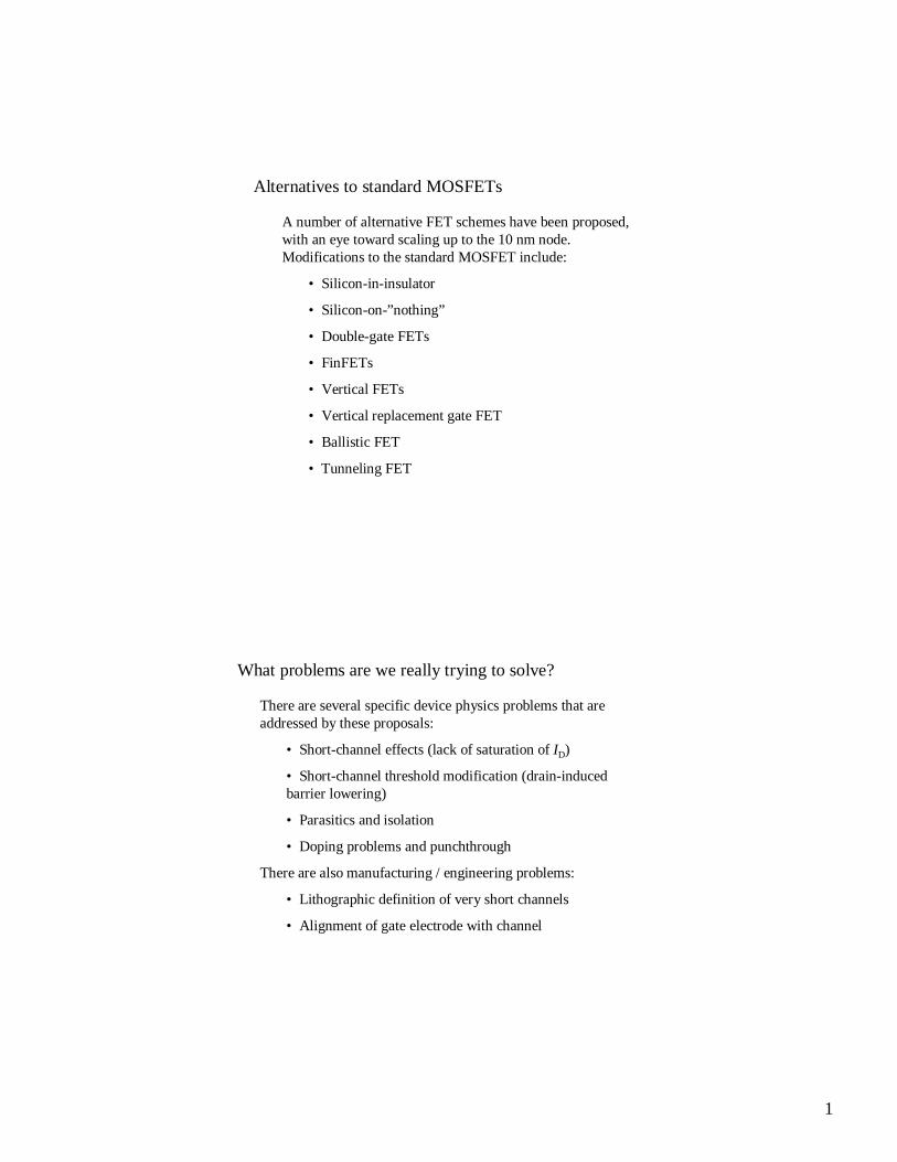
Another version of this is the FinFET:
• Uses a thin “fin” of Si as the channel, and wraps the gate around/over the fin.
• Allows large (low resistance) source & drain contacts.
6
FinFET
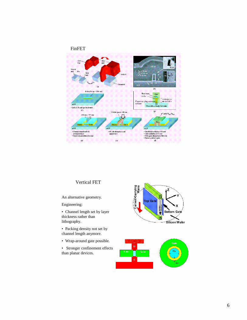
Vertical FET
An alternative geometry.
Engineering:
• Channel length set by layer thickness rather than lithography.
• Packing density not set by channel length anymore.
• Wrap-around gate possible.
• Stronger confinement effects than planar devices.
7
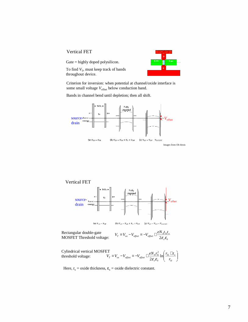
Vertical FET
Gate = highly doped polysilicon.
To find VT, must keep track of bands throughout device.
Images from Oh thesis
Voffset
Criterion for inversion: when potential at channel/oxide interface is some small voltage Voffset below conduction band.
Bands in channel bend until depletion; then all shift.
source-drain
Vertical FET
Voffsetsource-drain
Rectangular double-gate MOSFET Threshold voltage: 02 εε x
xSiAoffsetoffsetoxT
tteNVVVV +−=−=
Cylindrical vertical MOSFET threshold voltage: ++−=−=
Si
xSi
x
SiAoffsetoffsetoxT r
trreNVVVV ln
2 0
2
εε
Here, tx = oxide thickness, εx = oxide dielectric constant.
8
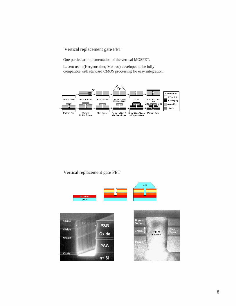
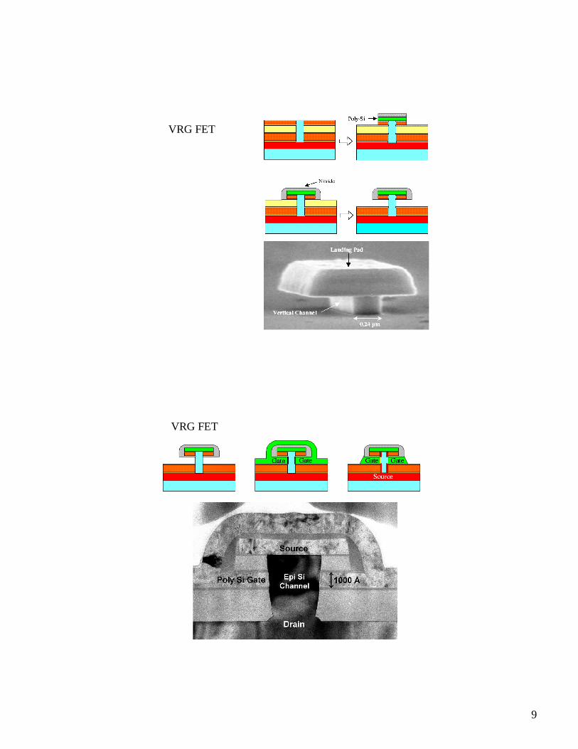
Vertical replacement gate FET
One particular implementation of the vertical MOSFET.
Lucent team (Hergenrother, Monroe) developed to be fully compatible with standard CMOS processing for easy integration:
Vertical replacement gate FET
9
VRG FET
VRG FET

10
Ballistic FETs
For smallest devices, it’s possible to make FETs with channels smaller / shorter than the elastic mean free path in Si.
Room temperature mobility ~ 200 cm2/Vs
Direction-averaged effective mass in Si ~ 0.31 m0
Result: τ ~ 3.5 x 10⁻¹⁴ s.
Assuming a nondegenerate source of carriers at room temperature, vT = thermal velocity ~ (2kBT/m*)1/2 = 1.7x10⁵ m/s.
Typical elastic mean free path: ~ 6 nm.
Next lecture we’ll go into these devices in more detail; merges with Landauer-Buttiker picture….
Tunneling FET
• Special case of a quantum-limited FET.
• We already know tunneling probability depends exponentially on barrier height.
• We also know effective barrier can be controlled using a gate - essentially, carriers traversing the barrier region feel the (screened) gate potential.
• It’s possible to make a transistor where tunneling is the dominant transport mechanism.
Two examples:
• Double quantum well tunneling (Sandia)
• Metal-oxide-metal tunneling (ONR)

11
Tunneling FET
Downsides:
• Uses GaAs.
• Works at 77K.
• Requires thinned-down sample (back-side processing).
Upsides:
• Can be extremely fast (THz speeds).
• More functionality than just regular FET.
• No short-channel effects, effectively.
Metal tunneling FET
Start with metal strip (Ti, Al, Nb).
Use AFM to electrochemically oxidize a ~10-30 nm wide line across strip to act as tunnel barrier.
Substrate is gate in prototype.
Can get significant modulation of tunneling barrier.
Upsides: all metal (!), no short channel effects.
Downsides: labor intensive; fragile; not defect tolerant.
12
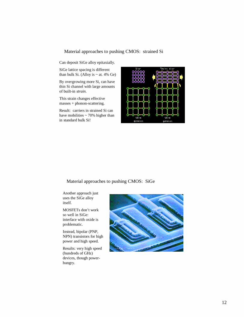
Material approaches to pushing CMOS: strained Si
Can deposit SiGe alloy epitaxially.
SiGe lattice spacing is different than bulk Si. (Alloy is ~ at. 4% Ge)
By overgrowing more Si, can have thin Si channel with large amounts of built-in strain.
This strain changes effective masses + phonon-scattering.
Result: carriers in strained Si can have mobilities ~ 70% higher than in standard bulk Si!
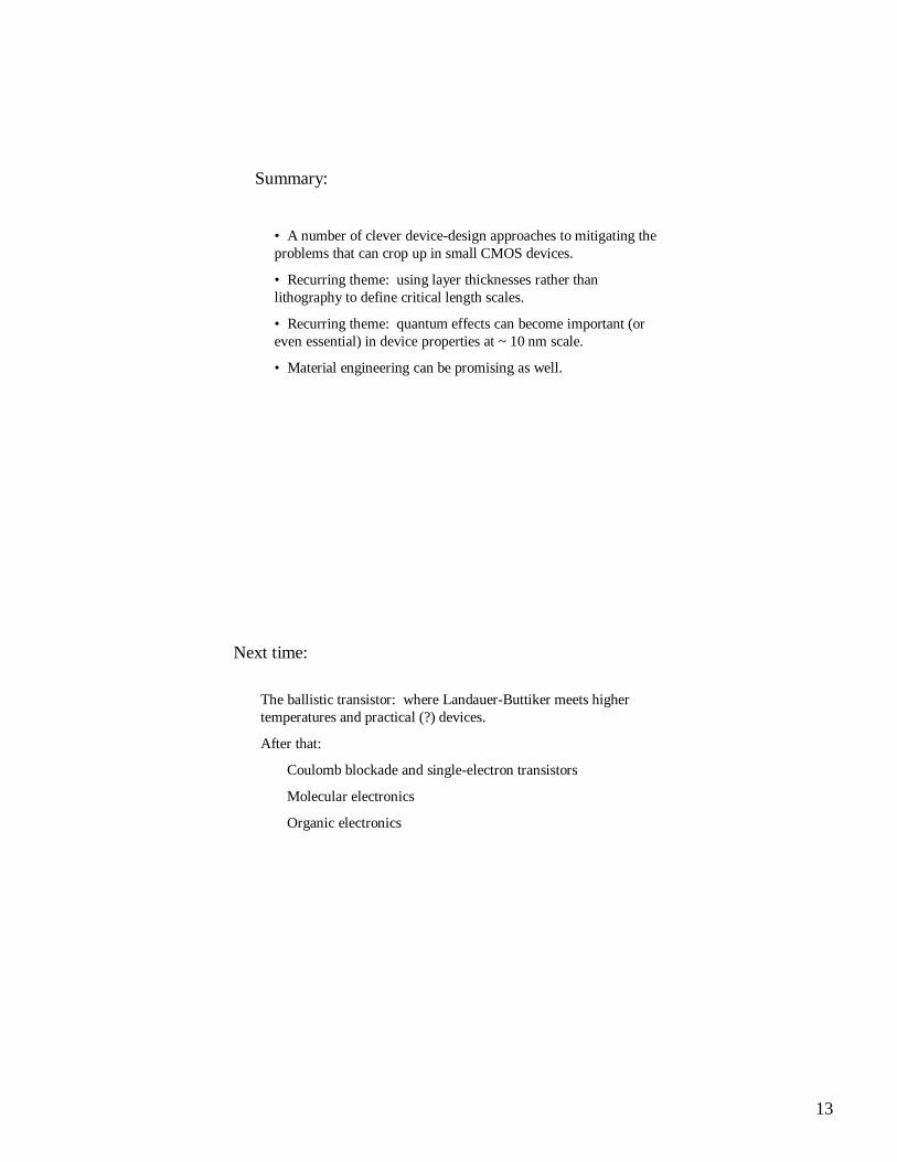
Material approaches to pushing CMOS: SiGe
Another approach just uses the SiGe alloy itself.
MOSFETs don’t work so well in SiGe: interface with oxide is problematic.
Instead, bipolar (PNP, NPN) transistors for high power and high speed.
Results: very high speed (hundreds of GHz) devices, though power-hungry.
13
Summary:
• A number of clever device-design approaches to mitigating the problems that can crop up in small CMOS devices.
• Recurring theme: using layer thicknesses rather than lithography to define critical length scales.
• Recurring theme: quantum effects can become important (or even essential) in device properties at ~ 10 nm scale.
• Material engineering can be promising as well.
Next time:
The ballistic transistor: where Landauer-Buttiker meets higher temperatures and practical (?) devices.
After that:
Coulomb blockade and single-electron transistors
Molecular electronics
Organic electronics


