
7725 N. Orange Blossom Trail • Orlando, FL 32810 • 407.298.7100 • [email protected] • www.micross.com
September 2013 • Revision 3.8
Micross provides comprehensive semiconductor packaging services for multiple electronic components, including digital, mixed signal, analog, multi-chip and System-in-Package (SiP). We design, build and test hermetic QML and chip scale packaging for various markets including down-hole, aerospace, satellite and military.
We combine advanced processes and product development to provide full turnkey support for prototype to volume production of flip chip and wire bond packages including single chip, multichip and SiP applications on organic substrates or ceramic substrates.
By ensuring delivery of finished wafers through our relationships with silicon OCMs, and full coordination of customer BOM requirements, we offer complete supply-chain management services for micro- electronic assemblies.
Micross supplies modules and contract assembly services for multiple platforms: industrial, airborne; commercial and government satellites; missile and ordnance; C4ISR and medical.
Custom & Multichip PackagingContract Manufacturing
Micross serves the defense aerospace, medical, industrial and space markets with these technologies. Design, assembly and test are performed in an on shore MIL-PRF-38535, MIL-PRF-38534 facility certified by DSCC to class V and H.
Micross’ contract assembly offers design and engineering support, BOM procurement, and a wide selection of package, substrate and interposer materials.
Micross Components can support your custom design with:
• Completeturnkeyproduct-includingprogramandvendormanagementofallelementsthroughouttheproductlifecycle
• Co-developmentofastatementofwork(SOW)
• Co-design,startingwithschematic,netlistorproductdefinitionanddocumentation
• Environmentalrequirementsreview
• Packageandmaterialselectionforoptimizationofelectricalandenvironmentalperformance,thermalmanagement,PCBsecondlevelreliabilityandcost
• Qualificationrequirementsvis-à-vispackagedefinition,electricaltestandcharacterizationexpectations
• Evaluationofthepowerrequirementsvs.proposedpackagedesign;analyzedinconjunctionwiththecreationoftheinitiallayout,dieplacementandfloorplanningandrouting
• Analysisofthermalandmechanicalelements
• Customerdefinedpackageandpinassignments
• Obsolescencemanagement
• Counterfeitmitigation
• DNAmarking
• Dierevisioncontrol
• Onshoredesign,assemblyandtest
• UseofCOTSstandardsiliconfromourdiedistributionpartners
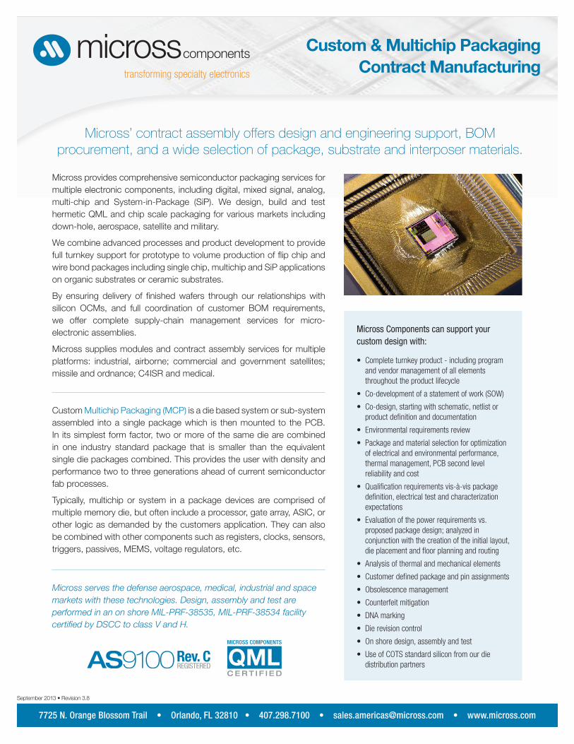
Custom Multichip Packaging (MCP) is a die based system or sub-system assembled into a single package which is then mounted to the PCB. In its simplest form factor, two or more of the same die are combined in one industry standard package that is smaller than the equivalent single die packages combined. This provides the user with density and performance two to three generations ahead of current semiconductor fab processes.
Typically, multichip or system in a package devices are comprised of multiple memory die, but often include a processor, gate array, ASIC, or other logic as demanded by the customers application. They can also be combined with other components such as registers, clocks, sensors, triggers, passives, MEMS, voltage regulators, etc.

7725 N. Orange Blossom Trail • Orlando, FL 32810 • 407.298.7100 • [email protected] • www.micross.com
September 2013 • Revision 3.8
Custom & Multichip PackagingContract Manufacturing
Facility and Quality
• DSCCQML
� MIL-PRF-38534, Class H (Class K in process)
� MIL-PRF-38535, Class Q
� MIL-PRF-38535, Class V (assembly)
� Laboratory Suitability (MIL-STD-883)
• SMD,QandMlevel
• CertificationofwafertraceabilitylottoClassHorClassKrequirements.
• Alldiepreparation,sampleassembly,evaluationandtestperTableC-IIin-housewithfulltraceabilityandMIL-STD-883DSCCLaboratoryCertification.
• NSTS5300.4
• CapabilitiesforClassSmanufacturing
• AS9100Rev.Cregistered
• Customerspecific,SourceControlDrawing(SCD)
Packaging Options
• Surfacemount
� Plastic Ball Grid Array (PBGA)
� Chip Scale Package (CSP)
� Ceramic and HiTCE Ceramic BGA
(see Table 1)
� Ceramic Flat Pack (FP)
� Ceramic Quad Flat Pack (CQFP)
� Ceramic gull wing
� Plastic, Small-Outline, J-leaded (CSOJ)
� SOJ, QFP, and TSOP as open cavity
� Plastic, Thin Quad Flat Package (TQFP)
� Ceramic Leadless Chip Carrier (CLCC)
Class 100 Clean Room
• Through-hole
� Pin Grid Array (PGA)
� Ceramic Dual-In-Line Package (CDIP)
� Zig-Zag in-line (ZIP)
� Metal can
Services
• Diebankingandpartsmanagement
• Totalturnkeymanufacturing,fullBOMmanagement
• DMS/obsolescencemitigation
• Diebankinganddiminishedsources(EndofLife)support.Microssdiebankisequippedwithstate-of-the-artclimatecontrolsystemsandnitrogen-purgeddryboxes.Westoreandhandleinventorypermilitary/industryspecificationsandprovideinternalclassAandBdieinspection.
• Obsoleteandlegacyproductssupport
• Flexible,personalizedcustomersupport
Engineering & Analytical Services
• ScanningElectronMicroscopy(SEM)
• Decapsulation
• Demarkingandinkorlasermark
• LotAcceptanceTesting
• Designofsubstrates,plastic/laminateorhermeticceramic
• Test,burn-inandqualification
• Visualinspectioninsuresdefectfreedieproducts
• Waferprobeinsurespost-assemblyintegrity
• Pickandplaceautomationforquickandprecisecustompackaging
• Componentevaluationandqualification
• Packageandsub-assemblydesign
• Devicecharacterization
• Infantmortalitytesting
• Sonoscan(CSAM),X-ray
• Studpull,bondpull
• Moistureresistance
• Steamage/solderability
• Saltspray
• Thermalshock/thermalanalysis
• PIND
• Leadfailure
• Temperaturecycling
• Hermetictesting
• Fineandgrossleaktest
• SPC,technicalsupport
• Centrifuge
• Mechanicalshockandvibration
Test
• Hotprobeto150°C
� Can be tooled for full functional test
� Capacity dependent on complexity of die and die/wafer
• Fulltemperatureupscreening
• Testingformemory,mixedsignal,LSI,VLSI,linear,logic,ASICs,RF,anddiscretes
• Customtestequipment
• Testequipment
� Agilent 83000
� Mixed Signal LTX Credence D10
� Memory test - Teradyne J937
� Teradyne A585
� Testronics 201 and FET9400
� Linear Test Systems LTX TS80
� ECL test system
� Delta flex pick & place handlers
� Symtek handlers - X1 & X4
� Temptronics temperature forcing systems (-65°C to +150°C capability)
� Automated Bench Test
• Fullstatic/dynamicburn-in
� Burn-in boards � Convection ovens � Static and dynamic Wakefield chambers

7725 N. Orange Blossom Trail • Orlando, FL 32810 • 407.298.7100 • [email protected] • www.micross.com
September 2013 • Revision 3.8
Custom & Multichip PackagingContract Manufacturing
Typical material properties of widely used interposers for multichip packaging
Material TCEThermal
ConductivityDielectric Constant
Typical Conductor Material
Description -40°C 25°C 125°C W/mK 1MHz 3.2GHz Description
HighTGlaminates(~300) 12-13 14-15 16-17 0.2 4.7 Cu
HighTCEceramic 8-8.5 8.5-9.0 10-11 2.0 9.4 9.5 Cu(paste)
AluminaceramicAl2O3 5 6 7 18 10 W
� AMBYX memory, large capacity ovens � AEHR ovens
Assembly
• 3DandadvancedICpackagingequipment
• Multi-chippackageormonolithic
• Morethan10,000sq.ft.ofcleanrooms
� Class 100
� Class 10,000
• Diematerials-Silicon,SOS,GaAs,SiC
• Baredieonmostsubstrates-FR4,Flex,LCP,BT,BN,Ceramic,Polyimide
• Encapsulation,transfermold,glob-topordamandfill
• Waferprocessing
� Wafer thinning to .004”
� Cut range up to 8” or 250mm2
� Die sorting - automatic pick and place
� Wafer maps converted/uploaded to ALPS for binning, sorting to gel pack, waffle pack, tape and reel, or directly packaged
• Automaticdieattach
� Eutectic
� Epoxy
� Solder
• Flip-chipattachassemblyincludingflux,highaccuracyplacement,reflowandprecisionautomatedcapillaryunderfill
• Mixedtechnologycombinationsofbaredieandpackagedpartsenablereducedformfactorsandcostmanagement
• Stateoftheartdieplacementmachine–placementaccuracyof±10µm
� Bonding capabilities include: gold ball, gold and aluminum wedge
• Auto/manualwirebonding
� K&S and F&K Delvotec automatic wire bonders
� 0.7 to 3.0 mil aluminum ultrasonic
� 0.7 to 2.0 mil gold thermosonic
� Heavy gauge 5 to 20 mil aluminum
• Bondpull-destruct/non-destruct
• Hermeticseal
� Gold-tin eutectic solder reflow
� Parallel seam seal
� Resistance welding – TO packages
� Glass frit seal
• Solderre-flow
• Vacuumbake
• Leadtrim/form
Multichip designs are assembled on aninterposerorsubstratetocreateacustomized,integrated product for a unique application.Within the multichip package, the designercan utilize bare die (wire bond or flip chip),WLCSP devices or stacked die. The criticalbenefitsofthistechnologyinclude:
• Greaterfunctionalityinafastertime-to-marketwindowthancouldbedonethroughsiliconintegrationorASICdevelopment.
• ReducedcostcomparedtoanASIC.
• IncreaseddensityandperformancewithreducedPCBareautilization;reduceddownroutingatthePCBlevelandreducedweight.ReduceddownroutingcanprovidepotentialPCBlayerreductionandlowerPCBcosts.
• Designoptimizationthroughuseofthemostcosteffectivesiliconsolutions;assemblingvarioussemiconductortechnologies,diegeometries,orsiliconfromdifferentfabsinthesamemultichippackage.
• Improvedsignalintegrityfromreducedtracelengths.
• ReducedPCBassemblycomplexityandwiderpitches,leadingtosimplifiedClass3PCBcompliance.
• AllowstheOEMtoupgradeproducts,meettechrefreshes,orpre-plannedproductimprovements,byusingdieshrinksinthesamepackage.
• Dependingonenvironmentalrequirements,theMCPcanbeinaceramichermeticorplasticencapsulatedpackages.

7725 N. Orange Blossom Trail • Orlando, FL 32810 • 407.298.7100 • [email protected] • www.micross.com
September 2013 • Revision 3.8
Custom Capabilities
Robotic Hot Solder Dipping & Solder ExchangeMicross SXT™ (Solder Exchange Technology) is a robotic, automated solder-dipping process developed by Micross Components to increase component reliability and mitigate tin-whisker formation. With Micross SXT™, unwanted finish can be replaced on a wide range of electronic components regardless of packaging style.
The GEIA-STD-0006 compliant process includes:
• Robotic-controlled six-axis dipping
• Solder dipping under a nitrogen blanket
• Solder-level sensing for accurate solder dipping
• Integral component wash and dry facility
• Preheating of components to negate thermal shock
• Lead tinning/solder dip
• Terminal finish conversion
• Solder exchange from Pb free (RoHS) ↔ SnPb
Anti-Counterfeit Program & BOM ManagementMicross Components is uniquely positioned to take a trusted role in your semiconductor supply chain to provide a counterfeit-free purchasing experience. Throughout our 35+ year history of providing authentic
high-reliability products, we’ve developed the software and the skills needed to handle everything from diodes to microprocessors.
If counterfeit protection is what you’re looking for... Get Real. Get Micross.
Hi-Rel Lead Attach
• Thermocompression weld lead
and high-temp solder lead
attachment processes
• J, Gullwing, and Spider Gullwing
lead forms
Trim & Form Components
• Trim, form, and solder dip to SOIC,
SOJ packages (other packages
not limited to DIP, PSOP, TSOP,
FP’s and QFP’s)
• Realign and Reform
Component Leads
3D Scanning Tape & Reel
BGA Modifications
• BGA re-balling for conversion
to tin-lead (SnPb)
• Ball attach
• BGA re-work
Test
• X-ray fluorescence
analysis (XRF)
• Ionic cleanliness test
• Solderability testing
• Particle Impact Noise Detection
test (PIND)
• Fine and gross leak testing
• Lead integrity/bond strength


