
INNOVATIONS TO ADDRESS POWER AND COST CHALLENGES OF
CURRENT AND EMERGING MARKETS FOR SEMICONDUCTOR DEVICES
VP Strategic Partnerships, North AmericaSpecial thanks to Séverine Cheramy, Fabien Clermidy, Mathilde Costes-Majorel,
Denis Dutoit, Daniel Gitlin, Jean-Eric Michallet,Maud Vinet

| 2
WELCOME TO GRENOBLE
Hughes Metras | The Confab l 06.13.2016
| 3
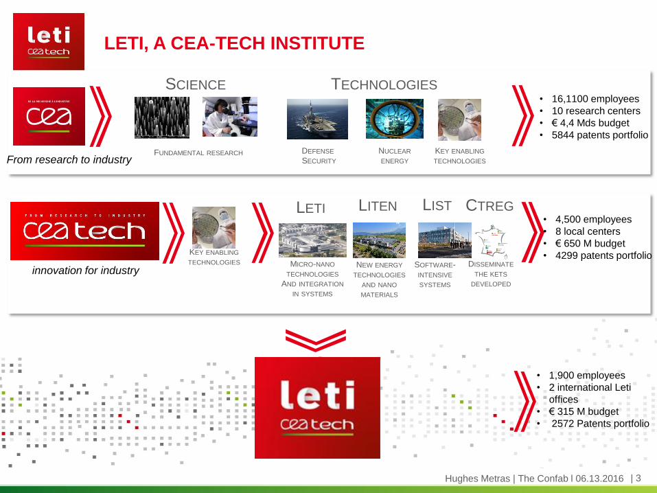
LETI, A CEA-TECH INSTITUTE
TECHNOLOGIES
DEFENSE
SECURITY
NUCLEAR
ENERGY
KEY ENABLING
TECHNOLOGIES
SCIENCE
FUNDAMENTAL RESEARCH
• 16,1100 employees
• 10 research centers
• € 4,4 Mds budget
• 5844 patents portfolio
innovation for industry
LETI LISTLITEN CTREG
KEY ENABLING
TECHNOLOGIES
• 4,500 employees
• 8 local centers
• € 650 M budget
• 4299 patents portfolioMICRO-NANO
TECHNOLOGIES
AND INTEGRATION
IN SYSTEMS
NEW ENERGY
TECHNOLOGIES
AND NANO
MATERIALS
SOFTWARE-
INTENSIVE
SYSTEMS
DISSEMINATE
THE KETS
DEVELOPED
From research to industry
• 1,900 employees
• 2 international Leti
offices
• € 315 M budget
• 2572 Patents portfolio
Hughes Metras | The Confab l 06.13.2016

| 4
: « CEA AT THE TOP OF THE LIST »
Hughes Metras | The Confab l 06.13.2016
| 5
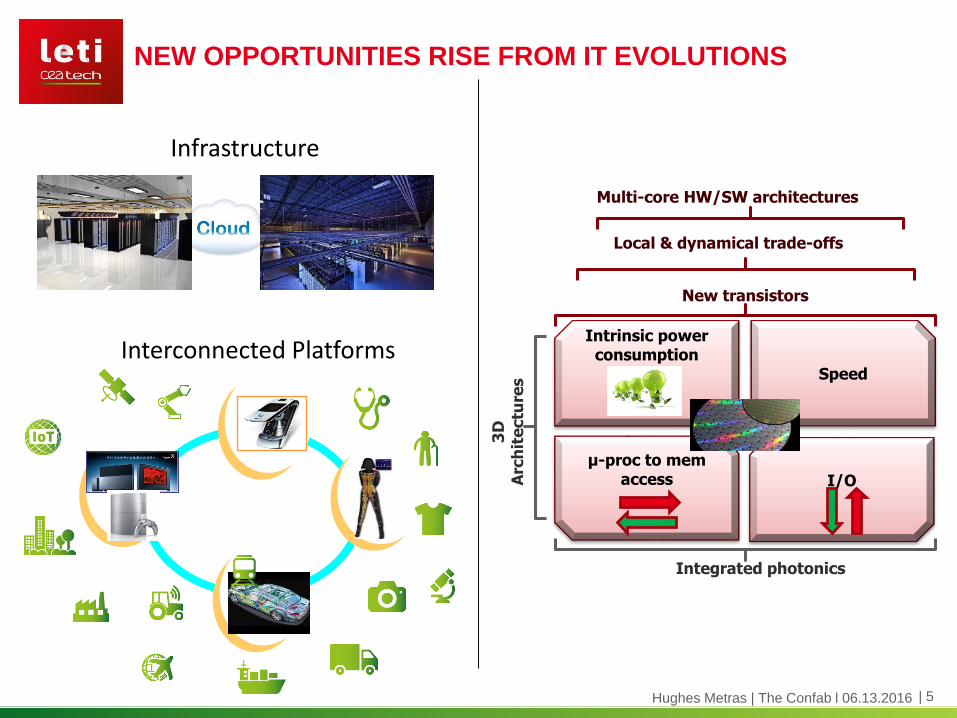
NEW OPPORTUNITIES RISE FROM IT EVOLUTIONS
Infrastructure
Interconnected Platforms
Hughes Metras | The Confab l 06.13.2016
I/O
µ-proc to memaccess
Intrinsic power consumption
Speed
New transistors
Local & dynamical trade-offs
Multi-core HW/SW architectures
Integrated photonics
3D
Arc
hit
ectu
res
| 6
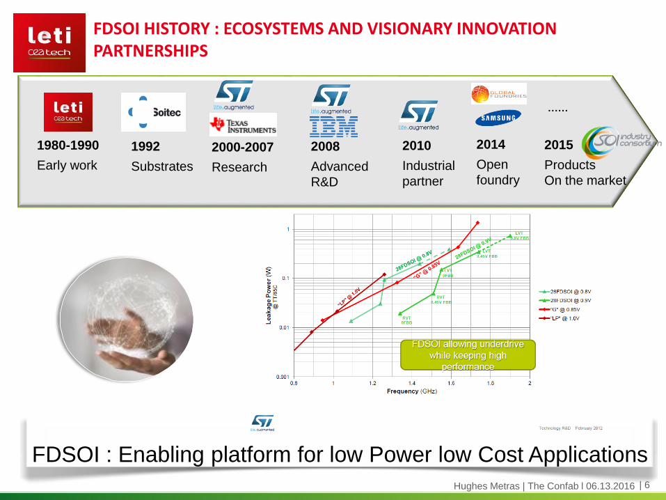
FDSOI HISTORY : ECOSYSTEMS AND VISIONARY INNOVATION PARTNERSHIPS
2000-2007
Research
2008
Advanced
R&D
2010
Industrial
partner
1992
Substrates
2014
Open
foundry
2015
Products
On the market
……
1980-1990
Early work
FDSOI : Enabling platform for low Power low Cost Applications
Hughes Metras | The Confab l 06.13.2016
| 7
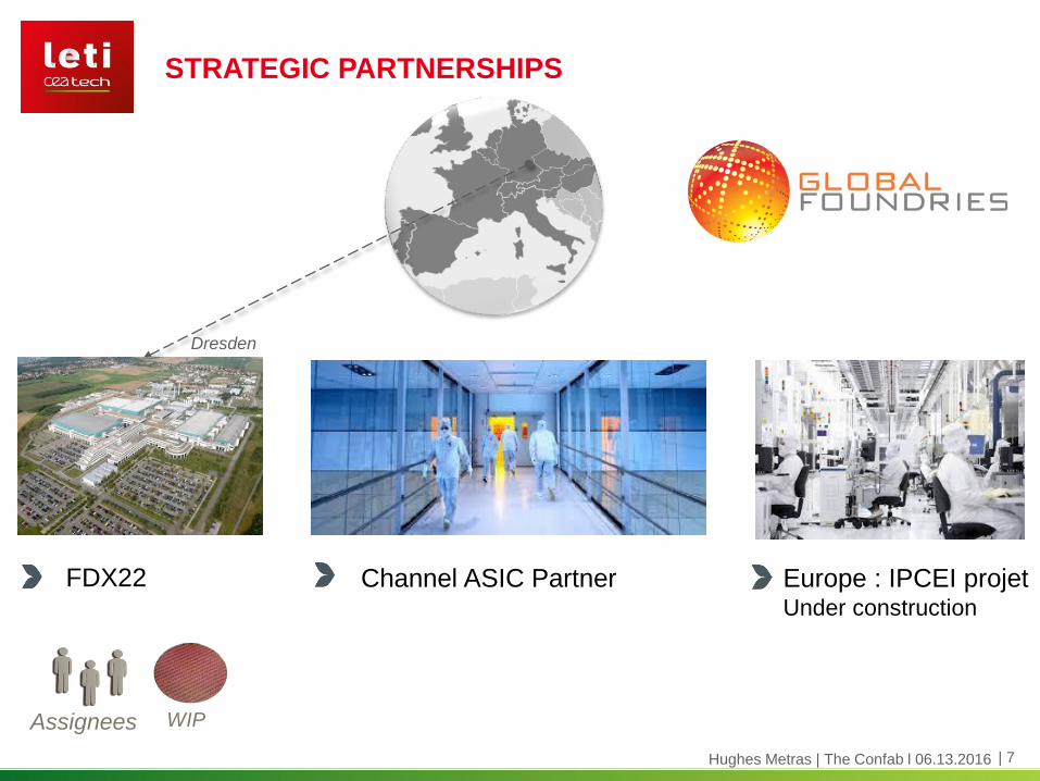
STRATEGIC PARTNERSHIPS
Europe : IPCEI projetUnder construction
Channel ASIC PartnerFDX22
Assignees WIP
Dresden
Hughes Metras | The Confab l 06.13.2016

| 8
ADVANCED CMOS ROADMAP
Early design coupling
28FDSOI
28nm
14nm
10nm
7nm
5nm
Evolutionary scaling: technology driven performance improvement
14FDSOI 10FDSOI
High mobility materials Ge and III-V
Non planar / trigate / stacked NW
Early material and
process
coupling
Mechanical switches
Hyb
rid
lo
gic
Steep slope devices
Single Electron Transistor
Disruptive scaling
Monolithic3D – M3D
FinFET
Alternative to scaling
Ge 10 nm
BOX
Si02
25nm TBOX
20nm LG ISPD SiCRSD
Si channel25nm TBOX
20nm LG ISPD SiCRSD
Si channel
Source
Drain
Gate
Fin
Source
Drain
Gate
Fin
Hughes Metras | The Confab l 06.13.2016

| 9
NEW OPPORTUNITIES IN 3D : COOLCUBE (3D VLSI)
At 14nm node, CoolCubeTM 3D via density D > 100 million vias/mm2
P. Batude et al, VLSI 2011
Bulk TSVSOI TSV
D = 10.000/mm 2D = 100.000/mm 2
D> 100.000.000/mm 2
D> 5.000.000/mm 2
CoolCubeTM
• Device scaling more and more difficult and costly (lithography, material, architecture)
• Global IC performance improvement without device scaling
• Natural opportunity for high-level integration
Hughes Metras | The Confab l 06.13.2016
| 10
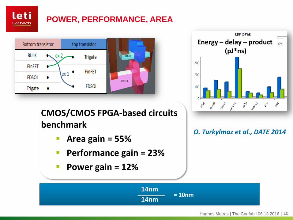
POWER, PERFORMANCE, AREA
Hughes Metras | The Confab l 06.13.2016
O. Turkylmaz et al., DATE 2014
CMOS/CMOS FPGA-based circuits benchmark
Area gain = 55%
Performance gain = 23%
Power gain = 12%
ex 1
ex 2 FDSOI
FinFET
14nm
14nm= 10nm
Energy – delay – product (pJ*ns)

| 11
COOLCUBE™ ADD-ON TO SCALING PATH
28nm
BEOL
PlanarHKMG
BEOLx2Pat
FinFet/PlanarHKMG
BEOLX3,4PatEUV?
FinFet/PlanarGe/III-VHKMG
14/16nm 10/11nm
CoolCube™ 28nm
NEW
R&D Cost
~500M$
CoolCube™ 14nm
1-2 B$
Cost
X2-3 ?
Cost
7/8nm
?X4-5 ?
Cost
CoolCube™ 10nm
CoolCubeTM offers more alternatives at a very affordable cost
Hughes Metras | The Confab l 06.13.2016
| 12
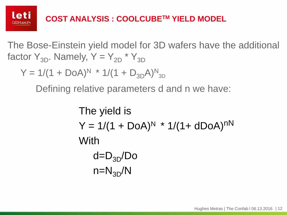
COST ANALYSIS : COOLCUBETM YIELD MODEL
• The Bose-Einstein yield model for 3D wafers have the additional
factor Y3D. Namely, Y = Y2D * Y3D
Y = 1/(1 + DoA)N * 1/(1 + D3DA)N3D
Defining relative parameters d and n we have:
The yield is
Y = 1/(1 + DoA)N * 1/(1+ dDoA)nN
With
d=D3D/Do
n=N3D/N
Hughes Metras | The Confab l 06.13.2016

| 13
PARTITIONING SCHEMES
Hughes Metras | The Confab l 06.13.2016

| 14
PARTITIONING SCHEMES AND COST
The cost of 3D/2D chips has three factors, the relative
wafer manufacturing cost (n+1), the gross die per wafer
ratio, and the yield ratio
The area reduction ratio a and the relative complexity n
are
Cell/Cell a~2, n~0.4-0.6
NMOS/PMOS a~1.67, n~0.1-0.2
Hughes Metras | The Confab l 06.13.2016

| 15
COOLCUBETM IMPACT ON COST
Cost Reduction+ is
extremely attractive
Up to 50% cost reduction
(large die), plus speed and
power improvements
Cost Reduction+ can be
a powerful technology to
boost 28nm, either by
reducing cost or adding
capability at same cost
Rela
tive d
ie c
ost
Co
olC
ub
eT
M
vs.
trad
itio
nal
pro
cess
Do = 0.1, N=24, a=2, d=1
Do = 0.1, N=24, a=1.67, d=1
Area (A) of 3D wafers in mm2
Cell/Cell
NMOS/PMOS
Hughes Metras | The Confab l 06.13.2016
| 16
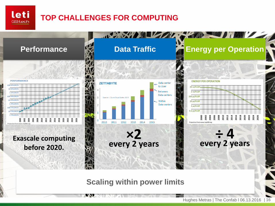
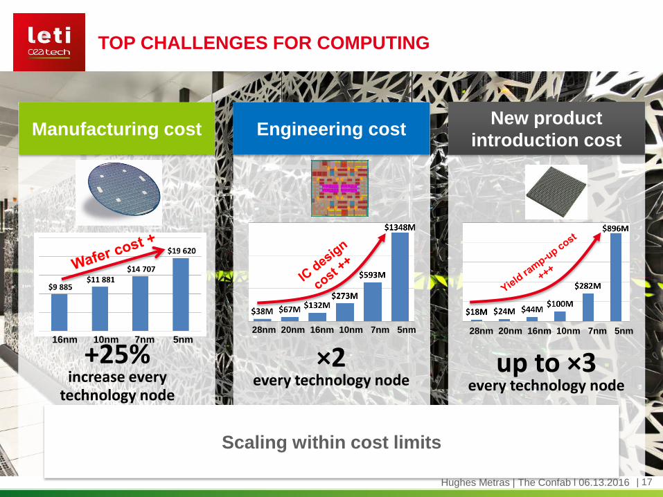
TOP CHALLENGES FOR COMPUTING
ENERGY PER OPERATION
20 nJ/FLOP
2 nJ/FLOP
200 pJ/FLOP
20 pJ/FLOP
2 pJ/FLOP
0.2 pJ/FLOP
20
00
20
01
20
02
20
03
20
04
20
05
20
06
20
07
20
08
20
09
20
10
20
11
20
12
20
13
20
14
20
15
20
16
20
17
20
18
20
19
20
20
20
21
20
22
20
23
20
24
20
25
20
26
20
27
Projection from www.top500.org
Energy per Operation
÷ 4 every 2 years
ZETTABYTE
Data Traffic
×2every 2 years
Scaling within power limits
PERFORMANCE
100 EFLOP/S
10 EFLOP/S
1 EFLOP/S
100 PFLOP/S
10 PFLOP/S
1 PFLOP/S
100 TFLOP/S
10 TFLOP/S
1 TFLOP/S
2000
2001
2002
2003
2004
2005
2006
2007
2008
2009
2010
2011
2012
2013
2014
2015
2016
2017
2018
2019
2020
2021
2022
2023
2024
2025
2026
2027
Projection from www.top500.org
Performance
Exascale computing before 2020.
Hughes Metras | The Confab l 06.13.2016
| 17
TOP CHALLENGES FOR COMPUTING
Manufacturing cost Engineering cost
Scaling within cost limits
New product
introduction cost
16nm 10nm 7nm 5nm
+25% increase every
technology node
28nm 20nm 16nm 10nm 7nm 5nm
×2every technology node
28nm 20nm 16nm 10nm 7nm 5nm
up to ×3every technology node
Hughes Metras | The Confab l 06.13.2016
| 18
Traditional
exponentially
growing “laws”
are running into
physical and cost
limits.Memory
Interconnect
System SW
Computing
THE NEED FOR NEW APPROACHES
$100M
$400M
$2000M
2015
2020
> 2020
0,1 EFLOP/s
200pJ/FLOP
1 EFLOP/s
20pJ/FLOP
10 EFLOP/s
2pJ/FLOP
PERFORMANCE
100 EFLOP/S
10 EFLOP/S
1 EFLOP/S
100 PFLOP/S
10 PFLOP/S
1 PFLOP/S
100 TFLOP/S
10 TFLOP/S
1 TFLOP/S
2000
2001
2002
2003
2004
2005
2006
2007
2008
2009
2010
2011
2012
2013
2014
2015
2016
2017
2018
2019
2020
2021
2022
2023
2024
2025
2026
2027
Projection from www.top500.org
ENERGY PER OPERATION
20 nJ/FLOP
2 nJ/FLOP
200 pJ/FLOP
20 pJ/FLOP
2 pJ/FLOP
0.2 pJ/FLOP
20
00
20
01
20
02
20
03
20
04
20
05
20
06
20
07
20
08
20
09
20
10
20
11
20
12
20
13
20
14
20
15
20
16
20
17
20
18
20
19
20
20
20
21
20
22
20
23
20
24
20
25
20
26
20
27
Projection from www.top500.org
Scaling within power limits
Scaling within cost limits
1. Cost: Disruptive architecture and integration technologies are required
2. Performance: Disruptive technologies are required
Hughes Metras | The Confab l 06.13.2016
| 19
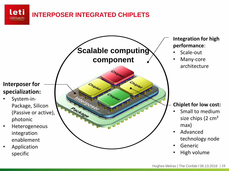
INTERPOSER INTEGRATED CHIPLETS
Integration for high performance:• Scale-out• Many-core
architecture
Scalable computing
component
Chiplet for low cost:• Small to medium
size chips (2 cm² max)
• Advanced technology node
• Generic• High volume
Interposer for specialization: • System-in-
Package, Silicon (Passive or active), photonic
• Heterogeneous integration enablement
• Application specific
Hughes Metras | The Confab l 06.13.2016

| 20
ExaNoDe will investigate, develop and
pilot:
• a highly efficient,
• highly integrated,
• high-performance,
• heterogeneous
compute element aimed towards
exascale computing.
Start date: October 2015.
CEA COORDINATES
THE H2020 EXANODE PROJECT
EXANODE
Chiplet
Interposer
3D-ICMulti-Chip-Module
Memory device
FPGA bare die
Candidate architecture for ExaNoDe
integration technology
Total budget: 8.6M€ Hughes Metras | The Confab l 06.13.2016

| 21
TECHNOLOGY
ARCHI-
TECTURE
& DESIGN
RESULTS
Silicon Interposer• Warp management
• TSV high aspect ratio
• Stress compensation
High density 3D• Chip-To-Chip fine pitch
• Die to Wafer stacking
3D integrated circuit• Modular 3D stack
processor
• 3D Building Blocks & libs.
Smal form factor: 20 µm pitch I/O
Low power: 1 pJ/b, Target: 20 pJ/FLOPS before 2020
3D learning: Process, Signal Integrity, Stress, Thermal, Reliability
High Bandwith density: 1 Tbps/mm²
Low-power, scalable
and low cost computing
components
3D SILICON INTEGRATION
[1] D. Dutoit, et al. "A 0.9 pJ/bit, 12.8 GByte/s WideIO Memory Interface in a 3D-IC NoC-
based MPSoC", VLSI Circuits (VLSIC), 2013 Symposium on , pp.C22,C23, 11-13 June 2013.
3D Silicon
Integration
Hughes Metras | The Confab l 06.13.2016
| 22
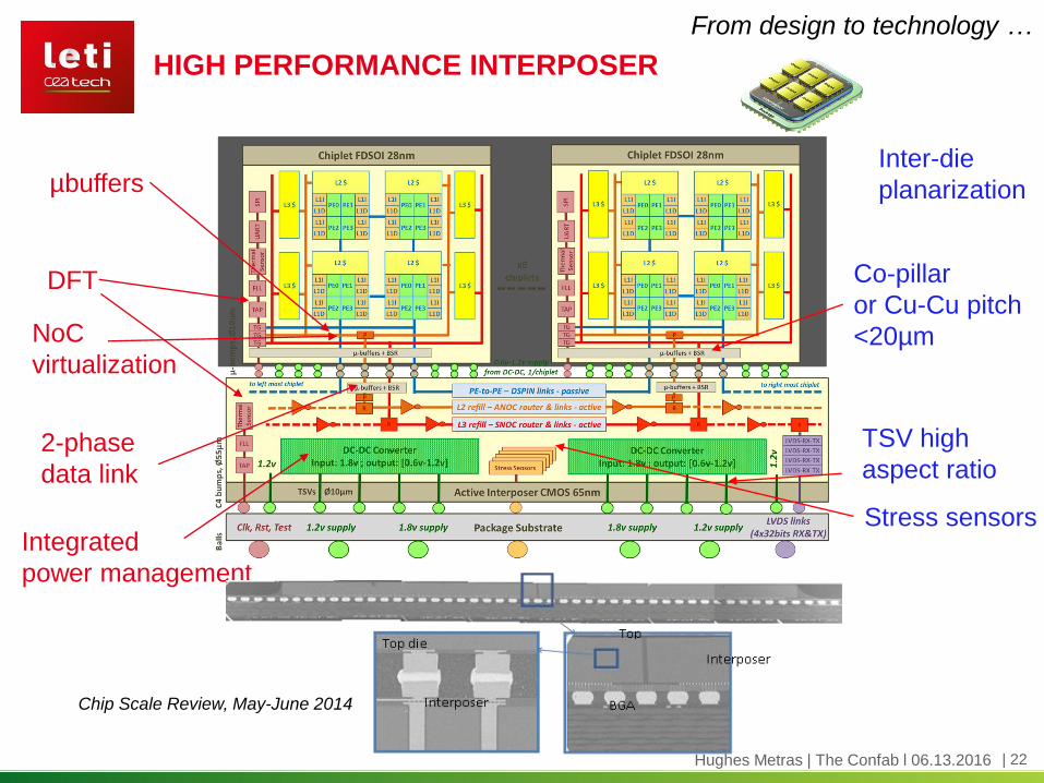
HIGH PERFORMANCE INTERPOSER
Inter-die
planarization
DFT
µbuffers
2-phase
data link
NoC
virtualization
TSV high
aspect ratio
Co-pillar
or Cu-Cu pitch
<20µm
Stress sensors
From design to technology …
Integrated
power management
Chip Scale Review, May-June 2014
Hughes Metras | The Confab l 06.13.2016
| 23
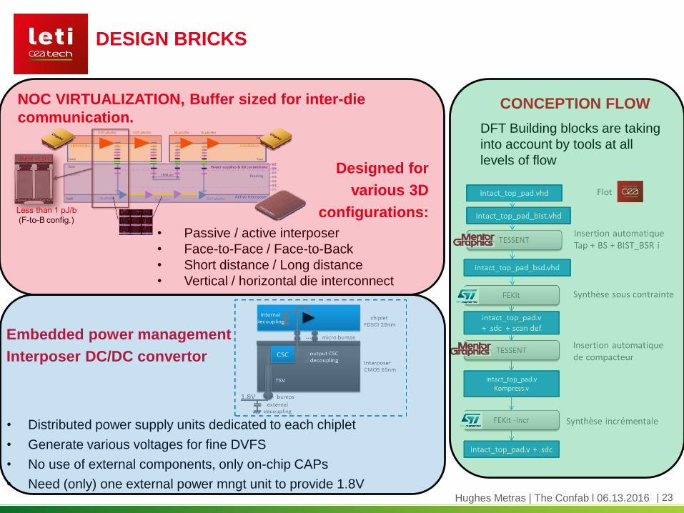
NOC VIRTUALIZATION, Buffer sized for inter-die
communication.
DESIGN BRICKS
Embedded power management
Interposer DC/DC convertor
• Distributed power supply units dedicated to each chiplet
• Generate various voltages for fine DVFS
• No use of external components, only on-chip CAPs
• Need (only) one external power mngt unit to provide 1.8V
Designed for
various 3D
configurations:
• Passive / active interposer
• Face-to-Face / Face-to-Back
• Short distance / Long distance
• Vertical / horizontal die interconnect
CONCEPTION FLOW
DFT Building blocks are taking
into account by tools at all
levels of flow
Hughes Metras | The Confab l 06.13.2016

| 24
SELF-ASSEMBLY AS FINE-PITCH ENABLER
Phase 1 : Self-alignment Phase 2 : Hybridation
Leti’s choice : Direct bonding Leti’s choice: capillary driven alignment Minimization of surface tension with capillary force
3 – REMOVAL OF THE TOP DIE
1 – LIQUID DEPOSITION ON
SUBSTRATE OR DIE
2 – ROUGH PRE-POSITIONNING
USING MECHANICAL TOOL
4 – SPONTANEOUS ALIGNMENT
THANKS TO CAPILLARY FORCE
5 – LIQUID EVAPORATION AND
HYBRIDATION
PRINCIPLE OF SELF-ASSEMBLY USING CAPILLARY FORCE
Hughes Metras | The Confab l 06.13.2016
| 25
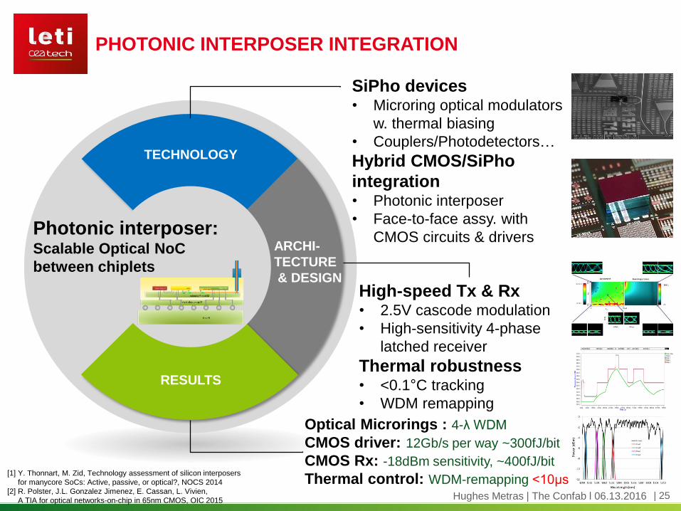
TECHNOLOGY
ARCHI-
TECTURE
& DESIGN
RESULTS
SiPho devices• Microring optical modulators
w. thermal biasing
• Couplers/Photodetectors…
Hybrid CMOS/SiPho
integration• Photonic interposer
• Face-to-face assy. with
CMOS circuits & drivers
High-speed Tx & Rx• 2.5V cascode modulation
• High-sensitivity 4-phase
latched receiver
Thermal robustness• <0.1°C tracking
• WDM remapping
Optical Microrings : 4-λ WDM
CMOS driver: 12Gb/s per way ~300fJ/bit
CMOS Rx: -18dBm sensitivity, ~400fJ/bit
Thermal control: WDM-remapping <10μs
Photonic interposer:Scalable Optical NoC
between chiplets
PHOTONIC INTERPOSER INTEGRATION
[1] Y. Thonnart, M. Zid, Technology assessment of silicon interposers
for manycore SoCs: Active, passive, or optical?, NOCS 2014
[2] R. Polster, J.L. Gonzalez Jimenez, E. Cassan, L. Vivien,
A TIA for optical networks-on-chip in 65nm CMOS, OIC 2015 Hughes Metras | The Confab l 06.13.2016
| 26
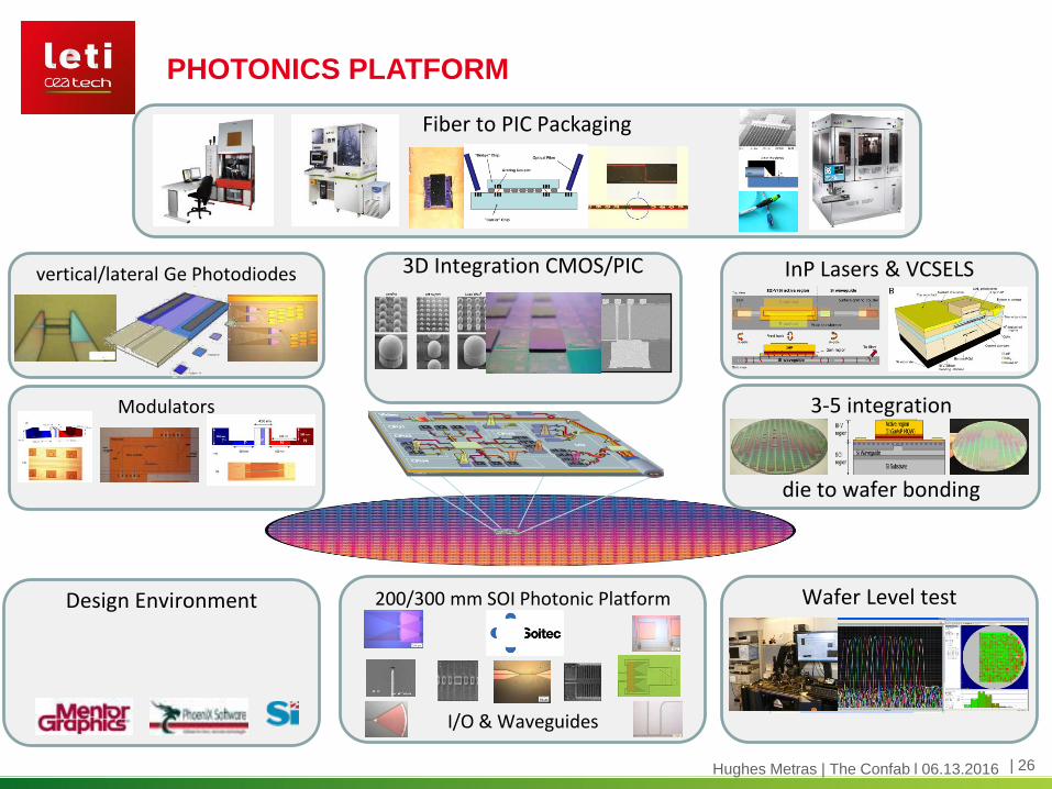
PHOTONICS PLATFORM
Design Environment 200/300 mm SOI Photonic Platform
I/O & Waveguides
Wafer Level test
Modulators
vertical/lateral Ge Photodiodes
3-5 integration
die to wafer bonding
InP Lasers & VCSELS3D Integration CMOS/PIC
Fiber to PIC Packaging
Hughes Metras | The Confab l 06.13.2016
| 27
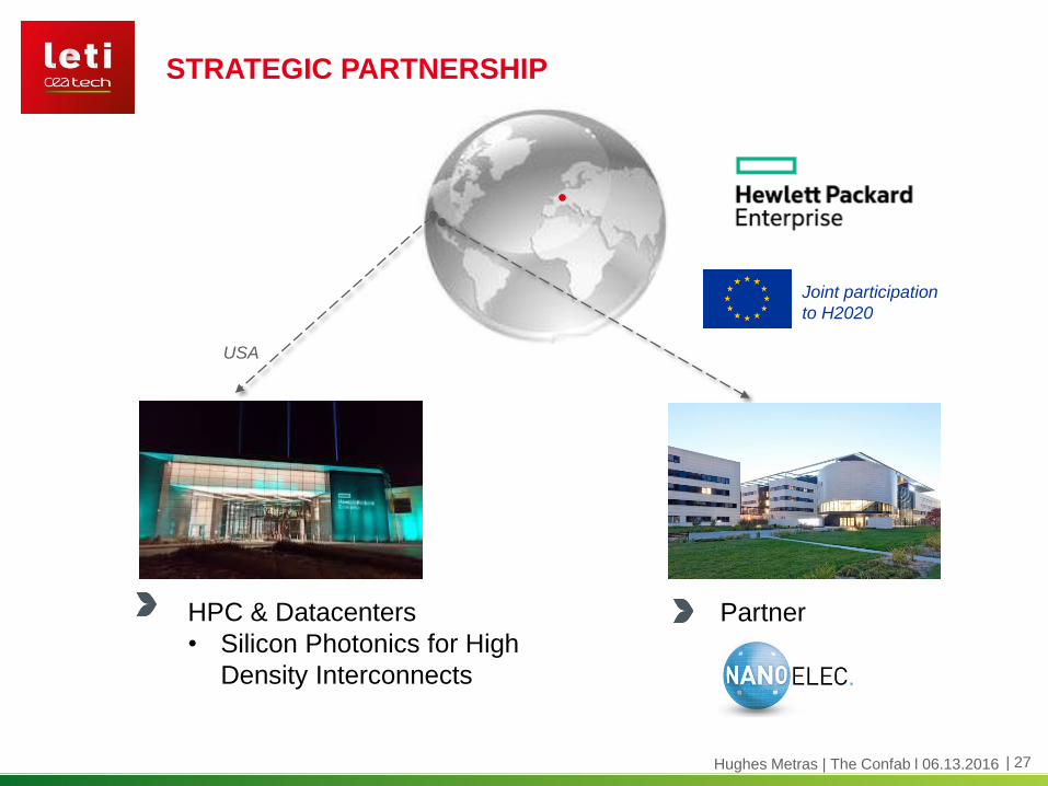
STRATEGIC PARTNERSHIP
HPC & Datacenters
• Silicon Photonics for High
Density Interconnects
Partner
USA
Joint participation
to H2020
Hughes Metras | The Confab l 06.13.2016
| 28
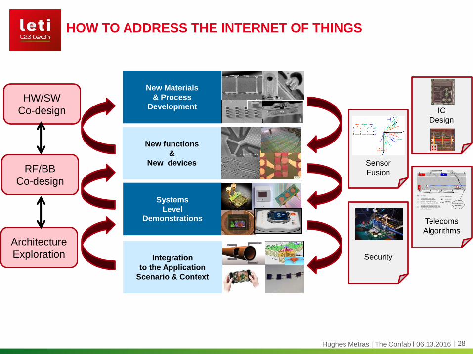
New Materials
& Process
Development
New functions
&
New devices
Systems
Level
Demonstrations
Integration
to the Application
Scenario & Context
HOW TO ADDRESS THE INTERNET OF THINGS
IC
Design
Sensor
Fusion
Telecoms
Algorithms
Streetlight
Parking sensor: Sensor node
with one transceiver (Digimesh)
Repeater: Sensor node with two
transceivers (Digimesh and 802.15.4)
Gateway: Node with communication with
sensor networks (Digimesh and 802.15.4)
and communication with external networks
(WiFi, GPRS, ethernet)
Load/Unload
Area
SmartSantander
Backbone
Digimesh Link
802.15.4 Link
WiFi/GPRS,
ethernet Link
Security
HW/SW
Co-design
RF/BB
Co-design
Architecture
Exploration
Hughes Metras | The Confab l 06.13.2016
| 29
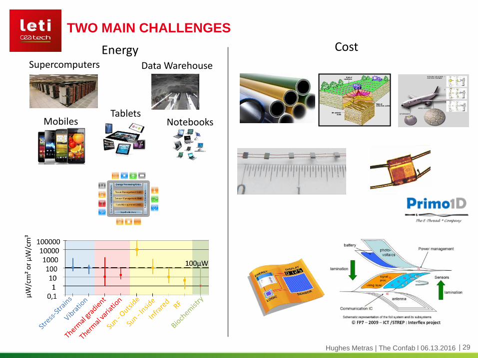
TWO MAIN CHALLENGES
Energy Cost
Mobiles Notebooks
Data WarehouseSupercomputers
Tablets
Hughes Metras | The Confab l 06.13.2016
| 30
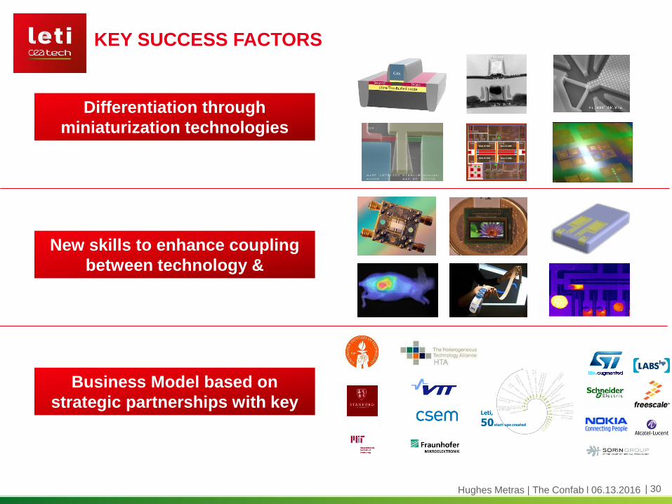
KEY SUCCESS FACTORS
Business Model based on
strategic partnerships with key
players
Differentiation through
miniaturization technologies
New skills to enhance coupling
between technology &
applications
Leti,
50start-ups created
Hughes Metras | The Confab l 06.13.2016

| 31
STRATEGIC PARTNERSHIPS
Wireless
Communication
Technologies
IOT Security Micro Displays
USA
Joint participation
to H2020,
Hughes Metras | The Confab l 06.13.2016
| 32
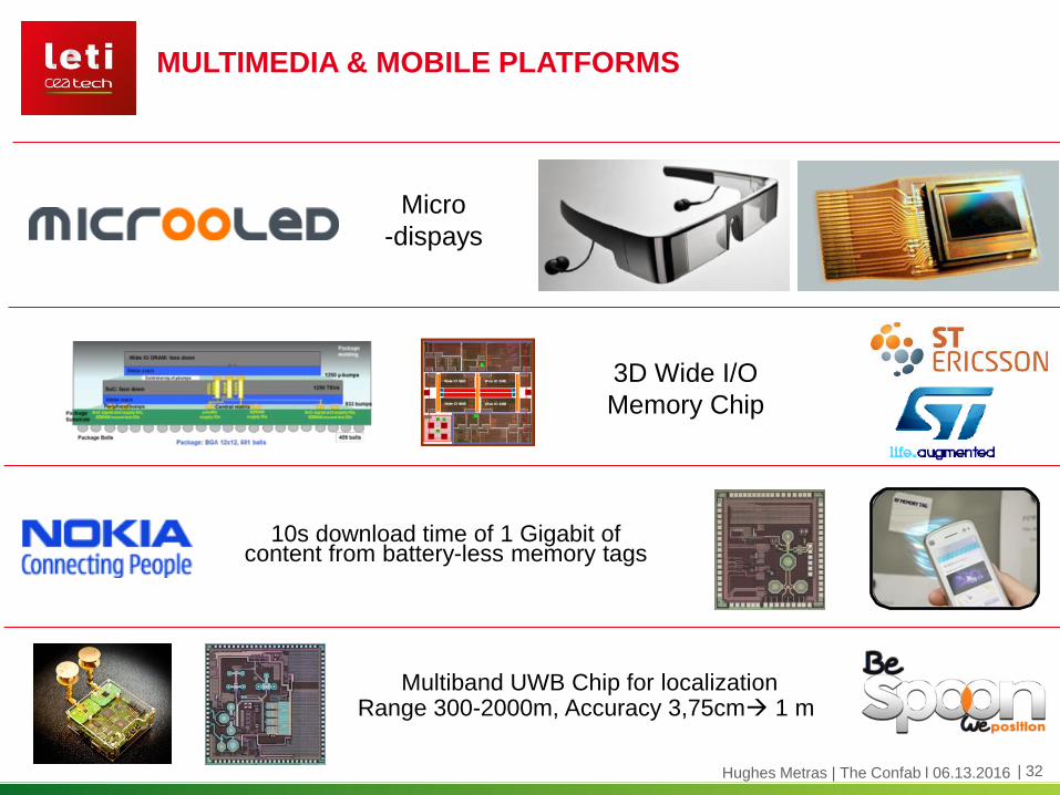
MULTIMEDIA & MOBILE PLATFORMS
Micro
-dispays
3D Wide I/O
Memory Chip
10s download time of 1 Gigabit of content from battery-less memory tags
Multiband UWB Chip for localizationRange 300-2000m, Accuracy 3,75cm 1 m
Hughes Metras | The Confab l 06.13.2016
| 33
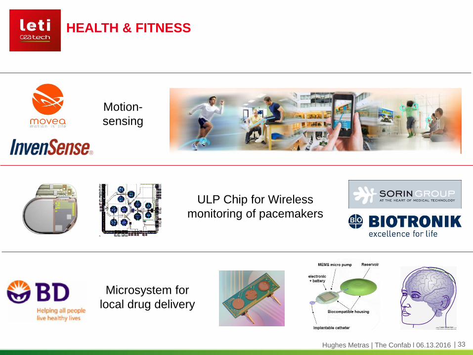
HEALTH & FITNESS
Motion-
sensing
ULP Chip for Wireless
monitoring of pacemakers
Microsystem for
local drug delivery
Hughes Metras | The Confab l 06.13.2016
| 34
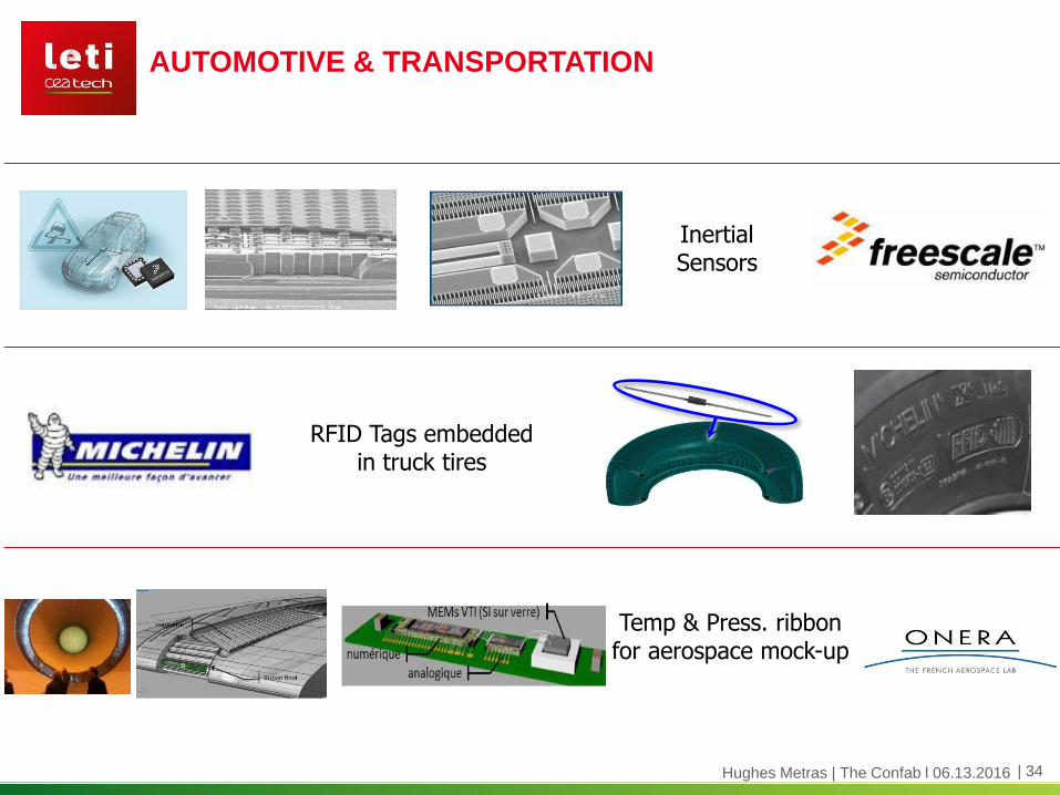
AUTOMOTIVE & TRANSPORTATION
RFID Tags embeddedin truck tires
Temp & Press. ribbon for aerospace mock-up
InertialSensors
Hughes Metras | The Confab l 06.13.2016
| 35
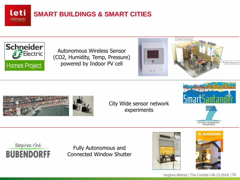
SMART BUILDINGS & SMART CITIES
Zonal Controller
Multi-Sensors
Autonomous Wireless Sensor (CO2, Humidity, Temp, Pressure)
powered by Indoor PV cell
City Wide sensor network experiments
Fully Autonomous andConnected Window Shutter
Hughes Metras | The Confab l 06.13.2016

| 36
INDUSTRY & INFRASTRUCTURES
Nanosensors
for
Gas analysis
Smart
Structures
Hughes Metras | The Confab l 06.13.2016
THANKS!
QUESTIONS?
|
P
37


