
Optical Interconnect Project
Phase 2 Brice Achkir/ Cisco and M.Immonen/ TTM
Feb 26th, 2014
Member Meeting ** San Jose** California
1
Outline
• HDP Optical Interconnect Project Phase 1
• Overview
• HDP Optical Interconnect Project Phase 2
• Definition and Directions
2 ©HDP User Group International, Inc.
Outline
• HDP Optical Interconnect Project Phase 1
• Outlook and Summary
• HDP Optical Interconnect Project Phase 2
• Definition and Directions
3 ©HDP User Group International, Inc.
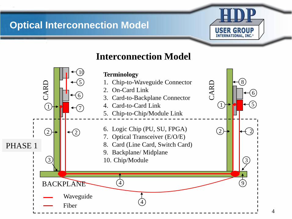
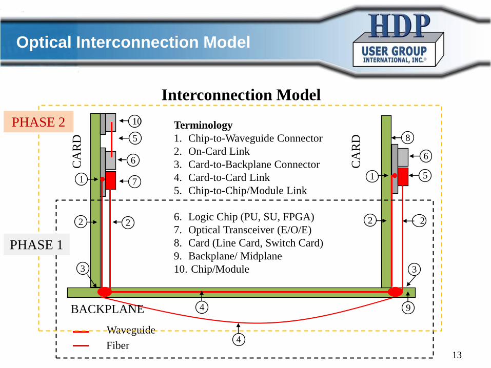
Optical Interconnection Model
4
Interconnection Model
1 1
2
Terminology
1. Chip-to-Waveguide Connector
2. On-Card Link
3. Card-to-Backplane Connector
4. Card-to-Card Link
5. Chip-to-Chip/Module Link
6. Logic Chip (PU, SU, FPGA)
7. Optical Transceiver (E/O/E)
8. Card (Line Card, Switch Card)
9. Backplane/ Midplane
10. Chip/Module
8
6 6
4
3
9
CA
RD
CA
RD
BACKPLANE
3
5
2
4
2
5 7
10
Fiber
Waveguide
2
PHASE 1
Description : TV1 (Phase 1)
• TV1 comprise of three distinct test vehicles used to verify design
parameters and connectivity options for practical applications and
Phase II demonstrator
• Two PCB design variants –
• Small mixed signal PCB 8” (Waveguide/Copper)
• Large 12”x18” PCB Backplane (Copper only)
• Two universal paddle card designs to test electrical end-to-end
link parameters (provided by Cisco)
• Optical testing via externally launched test source and fiber-optic
ribbons (passive optical test board)
• Multimode λ = 850 nm VCSELs/PDs
• Results provide verified performance parameters for on-board
copper and optical waveguide links
• Results provide direct copper-to-optical comparison metrics (SI,
loss, cross-talk, density) in equal base (laminate, construction)
5 ©HDP User Group International, Inc.
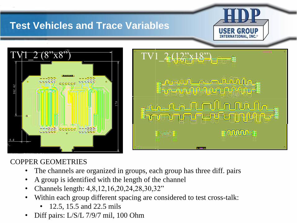
Test Vehicles and Trace Variables
6 ©HDP User Group International, Inc.
COPPER GEOMETRIES
• The channels are organized in groups, each group has three diff. pairs
• A group is identified with the length of the channel
• Channels length: 4,8,12,16,20,24,28,30,32”
• Within each group different spacing are considered to test cross-talk:
• 12.5, 15.5 and 22.5 mils
• Diff pairs: L/S/L 7/9/7 mil, 100 Ohm
TV1_2 (12”x18”) TV1_2 (8”x8”)
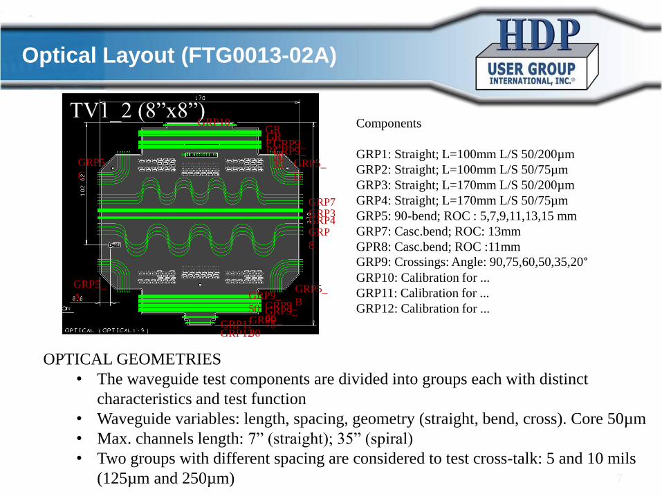
Optical Layout (FTG0013-02A)
7
GR
P1 GR
P2 GRP9_
20 GRP9_
35
GRP7
GRP
8
GRP9_
50 GRP9_
60 GRP9_
75 GRP9_
90
GRP5_
D
GRP5_
C
GRP5_
A GRP5_
B
GRP3 GRP4
Components
GRP1: Straight; L=100mm L/S 50/200µm
GRP2: Straight; L=100mm L/S 50/75µm
GRP3: Straight; L=170mm L/S 50/200µm
GRP4: Straight; L=170mm L/S 50/75µm
GRP5: 90-bend; ROC : 5,7,9,11,13,15 mm
GRP7: Casc.bend; ROC: 13mm
GPR8: Casc.bend; ROC :11mm
GRP9: Crossings: Angle: 90,75,60,50,35,20° GRP10: Calibration for ...
GRP11: Calibration for ...
GRP12: Calibration for ...
GRP10
GRP11 GRP12
OPTICAL GEOMETRIES
• The waveguide test components are divided into groups each with distinct
characteristics and test function
• Waveguide variables: length, spacing, geometry (straight, bend, cross). Core 50µm
• Max. channels length: 7” (straight); 35” (spiral)
• Two groups with different spacing are considered to test cross-talk: 5 and 10 mils
(125µm and 250µm)
TV1_2 (8”x8”)
Outline
• HDP Optical Interconnect Project Phase 1
• Outlook and Summary
• HDP Optical Interconnect Project Phase 2
• Definition and Directions
8 ©HDP User Group International, Inc.
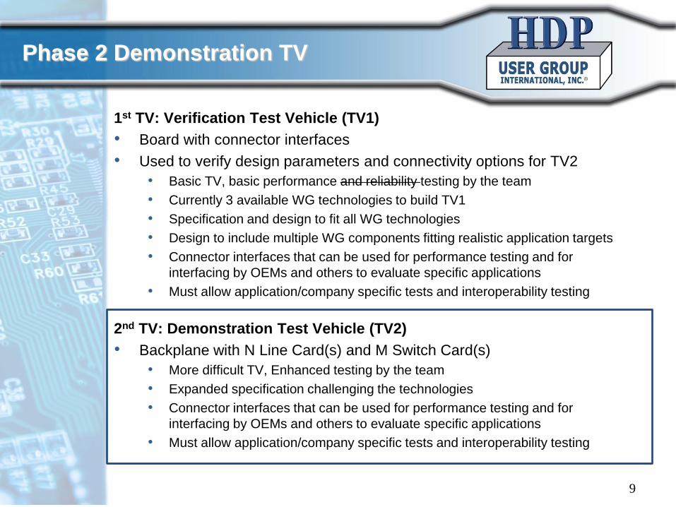
Phase 2 Demonstration TV
1st TV: Verification Test Vehicle (TV1)
• Board with connector interfaces
• Used to verify design parameters and connectivity options for TV2
• Basic TV, basic performance and reliability testing by the team
• Currently 3 available WG technologies to build TV1
• Specification and design to fit all WG technologies
• Design to include multiple WG components fitting realistic application targets
• Connector interfaces that can be used for performance testing and for
interfacing by OEMs and others to evaluate specific applications
• Must allow application/company specific tests and interoperability testing
2nd TV: Demonstration Test Vehicle (TV2)
• Backplane with N Line Card(s) and M Switch Card(s)
• More difficult TV, Enhanced testing by the team
• Expanded specification challenging the technologies
• Connector interfaces that can be used for performance testing and for
interfacing by OEMs and others to evaluate specific applications
• Must allow application/company specific tests and interoperability testing
9
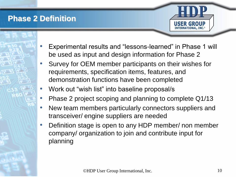
Phase 2 Definition
• Experimental results and “lessons-learned” in Phase 1 will
be used as input and design information for Phase 2
• Survey for OEM member participants on their wishes for
requirements, specification items, features, and
demonstration functions have been completed
• Work out “wish list” into baseline proposal/s
• Phase 2 project scoping and planning to complete Q1/13
• New team members particularly connectors suppliers and
transceiver/ engine suppliers are needed
• Definition stage is open to any HDP member/ non member
company/ organization to join and contribute input for
planning
10 ©HDP User Group International, Inc.
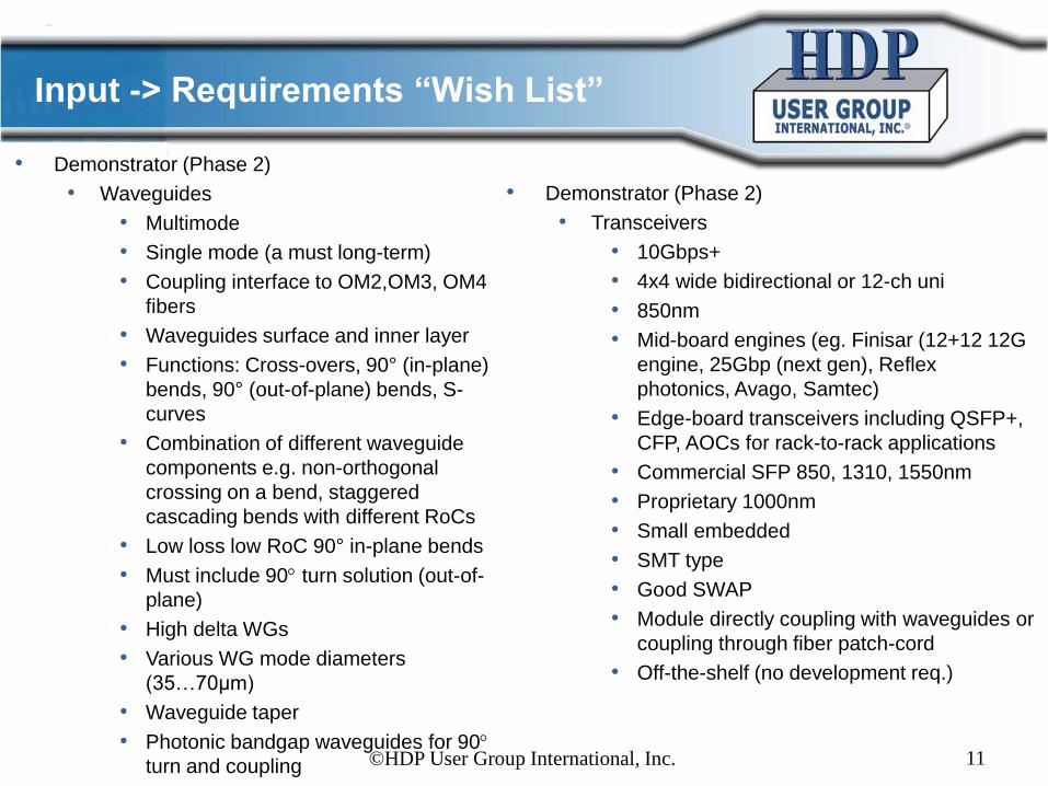
Input -> Requirements “Wish List”
11 ©HDP User Group International, Inc.
• Demonstrator (Phase 2)
• Waveguides
• Multimode
• Single mode (a must long-term)
• Coupling interface to OM2,OM3, OM4
fibers
• Waveguides surface and inner layer
• Functions: Cross-overs, 90° (in-plane)
bends, 90° (out-of-plane) bends, S-
curves
• Combination of different waveguide
components e.g. non-orthogonal
crossing on a bend, staggered
cascading bends with different RoCs
• Low loss low RoC 90° in-plane bends
• Must include 90 turn solution (out-of-
plane)
• High delta WGs
• Various WG mode diameters
(35…70µm)
• Waveguide taper
• Photonic bandgap waveguides for 90
turn and coupling
• Demonstrator (Phase 2)
• Transceivers
• 10Gbps+
• 4x4 wide bidirectional or 12-ch uni
• 850nm
• Mid-board engines (eg. Finisar (12+12 12G
engine, 25Gbp (next gen), Reflex
photonics, Avago, Samtec)
• Edge-board transceivers including QSFP+,
CFP, AOCs for rack-to-rack applications
• Commercial SFP 850, 1310, 1550nm
• Proprietary 1000nm
• Small embedded
• SMT type
• Good SWAP
• Module directly coupling with waveguides or
coupling through fiber patch-cord
• Off-the-shelf (no development req.)
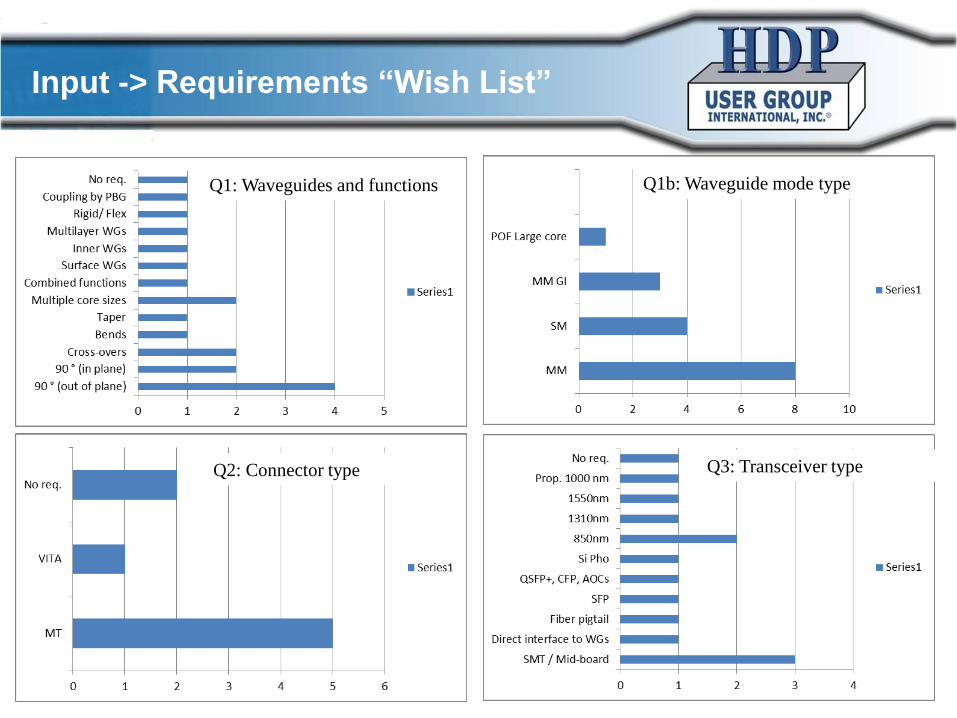
Input -> Requirements “Wish List”
Q1: Waveguides and functions Q1b: Waveguide mode type
Q2: Connector type Q3: Transceiver type
Optical Interconnection Model
13
Interconnection Model
1 1
2
Terminology
1. Chip-to-Waveguide Connector
2. On-Card Link
3. Card-to-Backplane Connector
4. Card-to-Card Link
5. Chip-to-Chip/Module Link
6. Logic Chip (PU, SU, FPGA)
7. Optical Transceiver (E/O/E)
8. Card (Line Card, Switch Card)
9. Backplane/ Midplane
10. Chip/Module
8
6 6
4
3
9
CA
RD
CA
RD
BACKPLANE
3
5
2
4
2
5 7
10
Fiber
Waveguide
2
PHASE 1
PHASE 2
Demonstration proposals
• Scope
• Demonstrate both non-orthogonal and orthogonal optical
solution similar to electrical backplane
• See/demo ability to plug modules into opto backplane
• Link length : > 30cm
• Short waveguide between ICs / long waveguide through a
backplane
• TV1 investigated separate waveguide geometries in isolation
i.e. just bends, just crossovers. In real routing applications
most waveguides will comprise a combination of different
waveguide components e.g. non-orthogonal crossing on a
bend, staggered cascading bends with different RoCs
depending on what obstacles need to be circumnavigated.
Demonstration proposals, cont.
• Implementation
• 1. Realistic “pseudo” product, optical routing
• Propose optical waveguide test designs for electro-optical boards
with electrically routed components on them, say server
motherboard or HPC or supercomputer controller.
• We don’t have to build a complete supercomputer board of
course, but if we used current PCB layout designs for HPCs or
supercomputers (whatever is available) and attempted to design
waveguides around them, then we would have a very good idea
of the typical real routing challenges that waveguides would face
in its first target application.
• The test vehicle could be just the waveguides minus the HPC /
server / supercomputer board in question.
• 2. Realistic “pseudo” product, form factor
• VMS/Eurocard form factors for at least one version of the test
vehicles
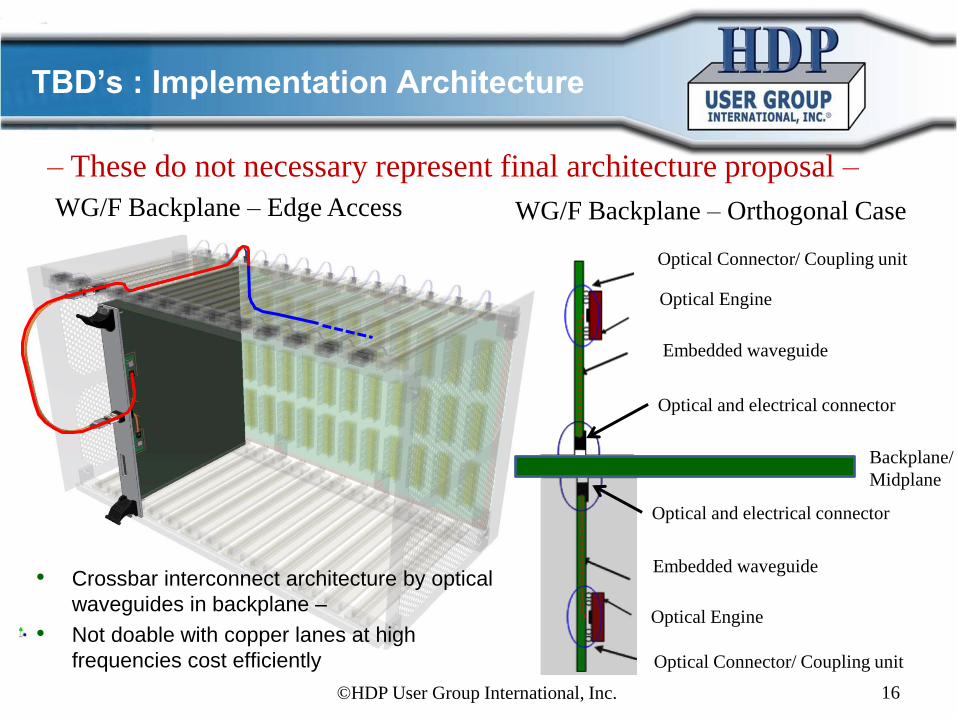
TBD’s : Implementation Architecture
16 ©HDP User Group International, Inc.
– These do not necessary represent final architecture proposal –
• Crossbar interconnect architecture by optical
waveguides in backplane –
• Not doable with copper lanes at high
frequencies cost efficiently
Optical Connector/ Coupling unit
Optical Connector/ Coupling unit
Optical Engine
Optical Engine
Embedded waveguide
Embedded waveguide
Optical and electrical connector
Optical and electrical connector
Backplane/
Midplane
WG/F Backplane – Edge Access WG/F Backplane – Orthogonal Case
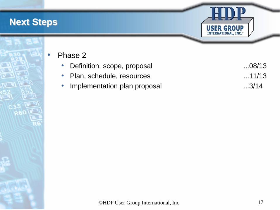
Next Steps
• Phase 2
• Definition, scope, proposal ...08/13
• Plan, schedule, resources ...11/13
• Implementation plan proposal ...3/14
17 ©HDP User Group International, Inc.
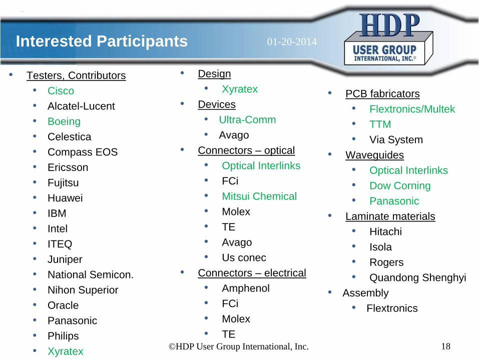
Interested Participants
18 ©HDP User Group International, Inc.
• Testers, Contributors
• Cisco
• Alcatel-Lucent
• Boeing
• Celestica
• Compass EOS
• Ericsson
• Fujitsu
• Huawei
• IBM
• Intel
• ITEQ
• Juniper
• National Semicon.
• Nihon Superior
• Oracle
• Panasonic
• Philips
• Xyratex
• Design
• Xyratex
• Devices
• Ultra-Comm
• Avago
• Connectors – optical
• Optical Interlinks
• FCi
• Mitsui Chemical
• Molex
• TE
• Avago
• Us conec
• Connectors – electrical
• Amphenol
• FCi
• Molex
• TE
• PCB fabricators
• Flextronics/Multek
• TTM
• Via System
• Waveguides
• Optical Interlinks
• Dow Corning
• Panasonic
• Laminate materials
• Hitachi
• Isola
• Rogers
• Quandong Shenghyi
• Assembly
• Flextronics
01-20-2014
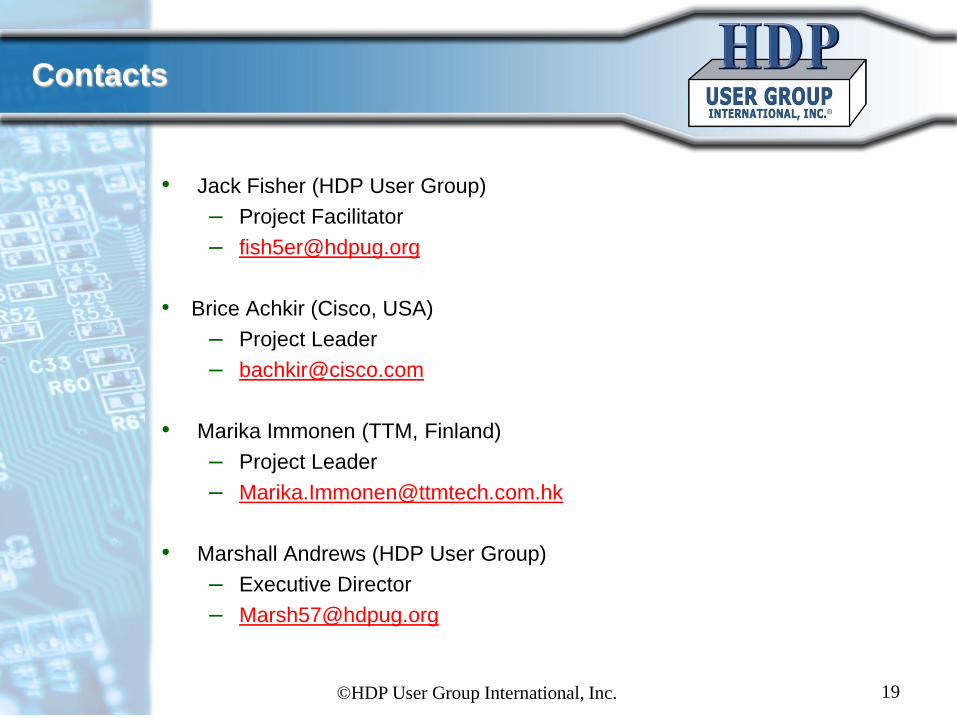
Contacts
• Jack Fisher (HDP User Group)
– Project Facilitator
• Brice Achkir (Cisco, USA)
– Project Leader
• Marika Immonen (TTM, Finland)
– Project Leader
• Marshall Andrews (HDP User Group)
– Executive Director
19 ©HDP User Group International, Inc.


