

1
Research Overview: Integration Challenges forPhotonics in the CMOS Platform
Mark A. BealsAssociate Director
MIT Microphotonics Center
MIT Microphotonics Center Fall MeetingOctober 20, 2006
2
Outline
EPIC Objective CMOS Technology Photonic Materials & Processing Device Integration Result Highlights Summary
This work was sponsored under the Defense Advanced Research Projects Agency'sEPIC Program and is executed by the Microsystems Technology Office (MTO)

3
Monolithic Electronic Photonic Integration• Objective
– Electronic Photonic Integration in the CMOS ProcessTechnology Platform
• Circuit driven optical link• High performance signal processing
– Mixed signal channelizers– Multicore processors– OADM– Transceivers Modulator
One Element ofA Filter Bank
Detector/TIA
Laser
300MHz to 2.2GHz RF
Detected Waveforms(Electrical)
Multimode InterferometricSplitter
OpticalChannelizer
Slice
4.5X Increase IBW95X Reduction Size
≥“
EPIC RF PhotonicChannelizer “Chip”
4.5X Increase IBW95X Reduction Size
80X Reduction in Weight5X Reduction in Power≥100X Reduction in Cost
“Nickel” Size
Bell LaboratoriesLucent TechnologiesBell LaboratoriesLucent Technologies

4
HIC Photonic Elements
Functions - Active and Passive Optical Devices• Routing• Mode transformers• MUX/DEMUX• Filters• Tuning• Modulation• Detection
Design Elements• Waveguides• Modulators• Splitters – MMI, Directional Couplers• Mode transformers• Interferometers• Resonators• OE conversion• Heaters
Optical Channellizer
Modulator
Filter n
Detector
Detector
TIA
TIA
LASER
DRIVER
RF IN
300 MHz to 2.2 GHzTUNING
Filter 1
Mul
ti-m
ode
Inte
rfero
met
ricS
plitt
er
EPIC

5
CMOS FabricationCMOS Logic Platform− 0.18 um Node− Silicon substrate− Oxide gate, SiO2− Salicide contacts, CoSi2− STI− Planarized ILD, SiO2− Interconnect – 7 Levels, AlCu− Vdd: 1.8V & 3.3V
3 Areas of Interest- Substrate- FEOL to PMD- BEOL – Metallization
Integration Priorities- FET Performance- Thermal cycling-proper sequencing- Cross Contamination- Process complexity
• PMD – SiO2, Planarized1.0µm
1.1µm
CMOS FET & Interconnect
• Silicon Substrate p-• Gate, S/D junctions
• Metal – AlCu,Local interconnectlevels 1-4
• IMD – SiO2, Planarized
• Contacts – W studs
• Vias – W studs
900
<550<450
*Salicide spike anneal 1050°C
750*• Salicide, Ti, Co

6
HIC Optical Waveguides – Silicon Core Materials
SOI waveguides achieved 0.35 dB/cmtransmission loss
State of the Art transmission loss for highlyconfined deposited waveguides ~4dB/cm
• CMOS Compatible• Single Crystal
− No bulk absorption, lowest loss− seed for EPI Ge, SiGe
• High Temperature tolerance
• CMOS Compatible• Low temperature PECVD film <450°C
− Integration in metal interconnect• Conversion to polysilicon >625°C
− Significant increase in lossGlobal Optical Interconnect ‘Local’ optical interconnect

7
1520 1540 1560 1580 1600 1620 1640
0.0
0.5
1.0
1.5
2.0
2.5
18
0 d
eg
ree
Be
nd
Lo
ss (
dB
/cm
)
Wavelength (nm)
r = 1 um r = 2 um r = 3 um r = 5 um r = 10 um
• Turn loss is higher in the TM mode• TE Mode enables more flexibility in routing• Thin TE waveguide integrates easily with CMOS
multi layer planarization
1520 1540 1560 1580 1600
0.0
0.5
1.0
1.5
2.0
2.5
18
0 d
eg
ree
Be
nd
Lo
ss (
dB
/cm
)Wavelength (nm)
r = 10 um
Waveguide Design – TE vs. TM
17% confinement
TE TM
180° Bend Loss

8
Mode Size vs. Geometry
• Waveguide dimensions should be maximized for maximum confinement• However, dimensions should be restricted to single-mode cutoff**Hybrid exception
TE Polarization – E field Contours
Simulated with FIMMWAVE0
0.5
1.0
1.5
2.0
2.5
3.0
0 0.5 1.0 1.5 2.0 2.5 3.0 3.5 4.0 4.5
200x200 nm2
neff = 1.473Γ = 0.044
200x500 nm2
neff = 2.365Γ = 0.716
5.00
0.5
1.0
1.5
2.0
2.5
3.0
0 0.5 1.0 1.5 2.0 2.5 3.0 3.5 4.0 4.5
200x200 nm2
neff = 1.473Γ = 0.044
200x500 nm2
neff = 2.365Γ = 0.716
5.0
Si Core, SiO2 Cladding

9
Waveguide Fabrication
• Substrate Leakage – f (Δn, h, w, tunderclad)• Absorption – f (α bulk, Δn, h,w)• Roughness Scattering – f (Δn, s, Λc h,w)
•Surface loss•Sidewall loss
Controlling Sources of Loss
Substrate/Underlayer
SiO2 tunderclad
SiO2
200nm
500nm
− Design > isolation design rules− Material & process method
− CMP− Etch & Post etch treatments
Si Optical Isolation VolumeConfined Mode – 200x500~ 10um3/per 1um length
~3.5um
~3umSiSiN ComparisonConfined Mode – 400x900~ 32um3/per 1um length

10
a-Si Annealeda-Si As Deposited
a-Si CMP
Processing α-Silicon Waveguides
Surface Scattering Loss Reduction
α-Si CMP removes surfaceroughness to <1nm rms

11
Active Photonic Device Materials & Processing
Ge Processing• Temperature 700C, 4.5h• Growth Rate = 2.4 nm/min• Roughness ~ 4nm rms
Ge UHV-CVD EPI Ge & SiGe Films
AFM of As Grown Ge Film
RIE Patterned GeTrench Filled &
CMP Planarization
Two New ‘Hot’ Processes for CMOS FEOL Integration

12
New Process Steps for “CMOS Front End” Photonic Integration
SiGe
M1
M2
M3
Heater
Deposited Si waveguide
LV
Via 2
Via 1
Contacts
SOI Waveguide
• Waveguide routing in SOI• SOI BOX optical isolation−Si wafer: Oxide filled trench optical
isolation, extension of STI• Planarized deposited waveguides &
cladding• Trench filled & planarized EPI SiGe
growth• n+ Top polysilicon electrode implant &
patterning• Resistive heater over tunable
elements
Polysilicon top SiGe electrodeSiGe Detector/Modulator
Metal 1
Metal 2
Metal 3
p+ implant (ldd)
n+ implant (ldd)
SiGe p-i-n Device Filter & Waveguides

13
Center Coupled Waveguide Integrated SiGe Detector
0.15 um Node9 mask levels
SiGe
Via
W Contacts & ILD
SOI Silicon Waveguide/Lower SiGe electrode
Metalinterconnect &IMD
α-Si Waveguide
Upper SiGe Electrode
BOX
Silicon Substrate
●
Edge View Side View
●
SOI CMOS Process using vertical input/output couplers
λ in λ out
n+
p+
CMOS Process flow enables multiple configurations for waveguide integration including:Bottom coupled, center coupled and top coupled waveguides
14
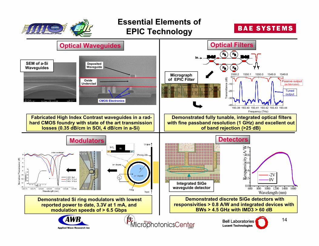
Essential Elements ofEssential Elements ofEPIC TechnologyEPIC Technology
Demonstrated fully tunable, integrated optical filterswith fine passband resolution (1 GHz) and excellent out
of band rejection (>25 dB)
In !=0.5R1 R2
R3 R4
!=0.5In !=0.5R1 R2
R3 R4
!=0.5
Optical Filters
-40
-30
-20
-10
0
Tra
nsm
itta
nce (
dB
)
193.44193.43193.42193.41193.40193.39
Frequency (THz)
1550.2 1550.1 1550.0 1549.9 1549.8
Tuned
output
Tuned
output
Tuned
output
Tuned
output
Passive output(as fabricated)
Passive output(as fabricated)
DetectorsModulators
Optical Waveguides
Demonstrated Si ring modulators with lowestreported power to date, 3.3V at 1 mA, and
modulation speeds of > 6.5 Gbps
600 800 1000 1200 1400 16000.0
0.2
0.4
0.6
0.8
1.0
Res
po
nsi
vit
y (
A/W
)
Wavelength (nm)
-2V 0V
Demonstrated discrete SiGe detectors withresponsivities > 0.8 A/W and integrated devices with
BWs > 4.5 GHz with IMD3 > 60 dB
Fabricated High Index Contrast waveguides in a rad-hard CMOS foundry with state of the art transmission
losses (0.35 dB/cm in SOI, 4 dB/cm in a-Si)
Oxide Underclad
DepositedWaveguide
CMOS Electronics
Integrated SiGewaveguide detector
Micrographof EPIC Filter
SEM of a-SiWaveguides
Bell LaboratoriesLucent TechnologiesBell LaboratoriesLucent Technologies

15
Technology Migration Challengesfor Monolithic Integration
• Integrated Designs– Limited Area availability– Use of 3D, new ‘optical plane– Electronic speed
• Improvement in Materials– Low temperature
• CMOS Technology to 32nm– Substrates
• SiGe• GeOI
– Feature size reduction– Cross contamination
• Contact metallurgy– Cu/Low K Interconnect
• Reduction in layerthickness
Altera/TSMC 90nm Cyclone II FPGACu Interconnect with CVD Low K
Source: Altera

16
AcknowledgementsEPIC Team• BAE Systems
– D. Carothers, T. Conway, J. Giunta, M. Gregory, M. Grove, C. Hill,M. Jaso, A. Pomerene
• Columbia University– C. W. Wong, R. Chatterjee, J. McMilan
• Cornell University– A. B. Apsel, M. Lipson, T. Kopa, Q. Xu
• Lucent Technologies – Bell Laboratories– Y.K. Chen, D. M. Gill, S. Patel, M. Rasras, K.Y. Tu, A. White
• MIT– L. C. Kimerling, D. Ahn, M. Beals, C. Hong, N. Jongthammanurak,
J. Liu, K. McComber, J. Michel, D. Pan, D. K. Sparacin, R. Sun,K. Wada
The early The early GeGe detector research was sponsored by Analog Devices, Inc. and Pirelli Lab, detector research was sponsored by Analog Devices, Inc. and Pirelli Lab, SpASpA


