19
1 2010 Litho ITRS Update Lithography iTWG Dec 2010
| Date post: | 10-Dec-2015 |
| Category: |
Documents |
| Upload: | anna-porter |
| View: | 214 times |
| Download: | 0 times |

1
2010 Litho ITRS Update
Lithography iTWG
Dec 2010

2
Outline
• 2010– Lithography Potential Solutions– Major Challenges
• 2011– Lithography Potential Solutions– Major Challenges– Some 2011 Update Focus
• Summary

3
2010 Updates
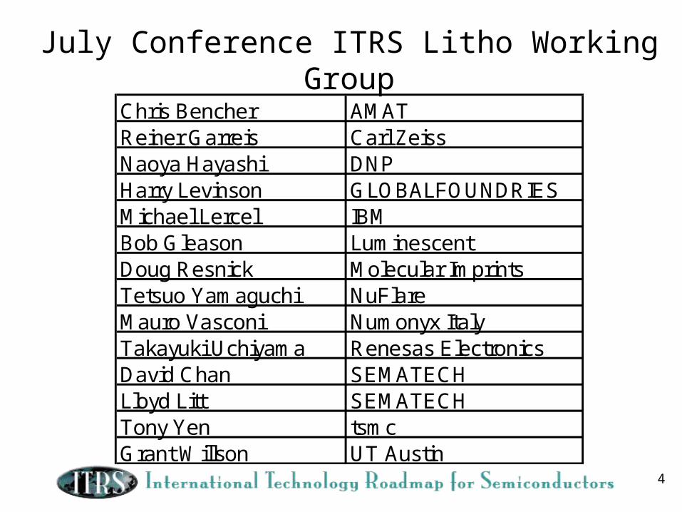
4
Chris Bencher AMATReiner Garreis Carl ZeissNaoya Hayashi DNPHarry Levinson GLOBALFOUNDRIESMichael Lercel IBMBob Gleason LuminescentDoug Resnick Molecular ImprintsTetsuo Yamaguchi NuFlare Mauro Vasconi Numonyx ItalyTakayuki Uchiyama Renesas ElectronicsDavid Chan SEMATECHLloyd Litt SEMATECHTony Yen tsmcGrant Willson UT Austin
July Conference ITRS Litho Working Group

5
First Year of IC Production 2009 2010 2011 2012 2013 2014 2015 2016 2017 2018 2019 2020 2021 2022 2023 2024
Flash ½ Pitch (nm) (un-contacted Poly)(f) 38 32 28 25 23 20 18 16 14 13 11 10 8.9 8.0 7.1 6.3
32 193 nm Immersion Double Pattern
22 193 nm Immersion Double Pattern
16193nm immersion Multiple Pattern
EUVImprint193nm immersion + DSAML2
11 EUV
193nm immersion Multiple Pattern
ImprintEUV + DSAInnovative patterning solution
Narrow Options
Narrow Options
NAND Flash Time Line
2010 28 & 25 nm HP

6
First Year of IC Production 2009 2010 2011 2012 2013 2014 2015 2016 2017 2018 2019 2020 2021 2022 2023 2024
DRAM ½ pitch (nm) (contacted) 52 45 40 36 32 28 25 23 20 18 16 14 13 11 10 9
MPU/ASIC Metal 1 (M1) ½ pitch (nm) 54 45 38 32 27 24 21 19 17 15 13 12 11 9.5 8.4 7.5
45193 nm Immersion with water
32193 nm Immersion Double PatternEUV
22 EUV193 nm Immersion Double / Multiple PatternML2 (MPU only)Imprint (DRAM only)
16 EUV193nm immersion Multiple PatternML2Imprint193nm immersion + DSA
11 EUVML2ImprintLitho + DSAInnovative patterning solution
Narrow Options
Narrow Options
Narrow Options
Narrow Options
MPU / DRAM time line

7
Difficult Challenges > / = 16nmEquipment infrastructure (writers, inspection, metrology, cleaning, repair) for fabricating masks with sub-resolution assist features
Registration, CD, and defect control for masks
Eliminating formation of progressive defects and haze during exposure
Understanding and achieving the specific signature and specifications for a Double Patterned mask
Establishing a stable process so that signatures can be corrected.
Overlay of multiple exposures including mask image placement, mask-to-mask matching, and CD control for edges defined by two separate exposuresAvailability of software to split the pattern, apply OPC, and verify the quality of the split while preserving critical features and maintaining no more than two exposures for arbitrary designsAvailability of high productivity scanner, track, and process to maintain low cost-of-ownership
Photoresists with independent exposure of multiple passes
Fab logistics and process control to enable low cycle time impact that efficient scheduling of multiple exposure passes.
Achieving constant/improved ratio of exposure related tool cost to throughput over time
ROI for small volume products
Resources for developing multiple technologies at the same time
Cost-effective resolution enhanced optical masks and post-optical masks, and reducing data volume
450 mm diameter wafer infrastructure if at 16nm
Optical masks with features for resolution enhancement and post-optical mask fabrication
Cost control and return on investment
Doluble and Multiple Patterning
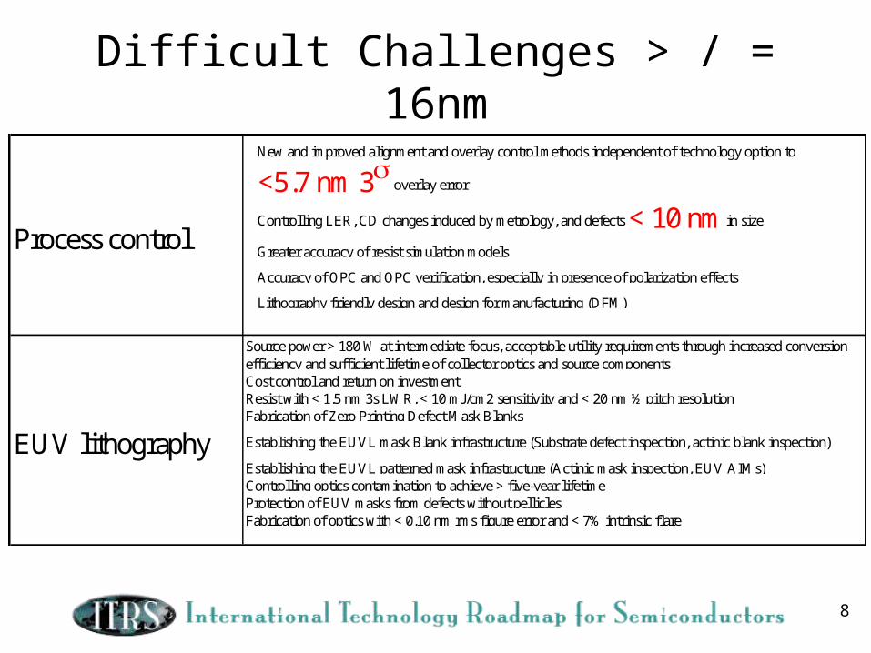
8
Difficult Challenges > / = 16nm
New and improved alignment and overlay control methods independent of technology option to
<5.7 nm 3s overlay error
Controlling LER, CD changes induced by metrology, and defects < 10 nm in size
Greater accuracy of resist simulation models
Accuracy of OPC and OPC verification, especially in presence of polarization effects
Lithography friendly design and design for manufacturing (DFM)
Source power > 180 W at intermediate focus, acceptable utility requirements through increased conversion efficiency and sufficient lifetime of collector optics and source componentsCost control and return on investmentResist with < 1.5 nm 3s LWR, < 10 mJ/cm2 sensitivity and < 20 nm ½ pitch resolutionFabrication of Zero Printing Defect Mask Blanks
Establishing the EUVL mask Blank infrastructure (Substrate defect inspection, actinic blank inspection)
Establishing the EUVL patterned mask infrastructure (Actinic mask inspection, EUV AIMs)Controlling optics contamination to achieve > five-year lifetimeProtection of EUV masks from defects without pelliclesFabrication of optics with < 0.10 nm rms figure error and < 7% intrinsic flare
EUV lithography
Process control

9
Difficult Challenges <16nm
NAhigher Source powerdouble patterning at EUV, flareResist incident angle
Different LTEM and absorber material to deal with high source power and heating
Limits of chemically amplified resist sensitivity for < 16 nm half pitch due to acid diffusion lengthMaterials with improved dimensional and LWR control add (limits)Resist and antireflection coating materials composed of alternatives to PFAS compoundsLow defects in resist materials (size < 10nm)Line width roughness < 1.4nm 3 sigma
Limits of chemically amplified resist sensitivity for < 16 nm half pitch due to acid diffusion lengthTimeliness and capability of equipment infrastructure (writers, inspection, metrology, cleaning, repair)
Increasingly long mask write and cycle time Mask process control methods and yield enhancementCost control and return on investment
Required degree of complexity with computational Lithography
Resist materials
EUV lithography - Extendibility
Mask fabrication

10
Difficult Challenges <16nmAchieving constant/improved ratio of exposure-related tool cost to throughputDevelopment of cost-effective post-optical masksCost effective 450mm lithography systemsAchieving ROI for small volume productsCost control and return on investmentWafer processing to tighter overlay and CD controlsMask fabrication to tighter specifications
Required degree of complexity with computational Lithography Increasing numbers of masks required.Defect inspection on patterned wafers for defects < 20 nmResolution and precision for critical dimension measurement down to 6 nm, including line width roughness metrology for 0.8 nm 3sMetrology for achieving < 2.8 nm 3s wafer overlay errorTemplate inspection for 1X Imprint Patterned MasksPhase shifting masks for EUV
193 nm Immersion Multilple Patterning
Metrology and defect inspection
Cost control and return on investment

11
Development of litho and post litho processes to control gate CD < 1.5 nm 3s with < 1.4 nm 3s line width roughness. Printed, post print process reduction, and final roughnessDevelopment of new and improved alignment and overlay control methods independent of technology option to achieve total < 2.8 nm 3s overlay error on products. especially for imprint lithography
Wafer ThroughputCost control and return on investmentDie-to-database inspection of wafer patterns written with maskless lithographyPattern placement - including stichingControlling variability between beams in multibeam systems
Defect-free Imprint templates at 1X dimensionsInfrastructure for 1X technology Templates (Write, inspection, and repair)Template fabrication to tighter specificationsProtection of Imprint templates from defects without pellicles
Mask Life timeThroughputCost control and return on investmentOverlayProcess control methods to compensate for systematic CD and overlay errors
Maskless Lithography
Imprint Lithography
Gate CD control improvements and process control
Difficult Challenges <16nm

12
Preliminary 2011 Updates

13
December Conference ITRS Litho Working Group
Reiner Garreis Carl ZeissBob Gleason LuminescentMasahiko Okumura NikonMauro Vasconi Numonyx ItalyTakayuki Uchiyama Renesas ElectronicsDavid Chan SEMATECHIwao Higashikawa Toshiba

14
First Year of IC Production 2010 2011 2012 2013 2014 2015 2016 2017 2018 2019 2020 2021 2022 2023 2024
Flash ½ Pitch (nm) (un-contacted Poly)(f) 32 28 25 23 20 18 16 14 13 11 10 8.9 8.0 7.1 6.3
32193 nm Immersion Double Pattern
22193 nm Immersion Double Pattern
16 EUV193nm immersion Multiple PatternImprint193nm immersion + DSA
11 EUV193nm immersion Multiple PatternEUV + DPImprint193nm immersion / EUV+ DSAInnovative patterning solution
Narrow Options
Narrow Options
NAND Flash Time Line
2010 28 & 25 nm HP

15
First Year of IC Production 2010 2011 2012 2013 2014 2015 2016 2017 2018 2019 2020 2021 2022 2023 2024
DRAM ½ pitch (nm) (contacted) 45 40 36 32 28 25 23 20 18 16 14 13 11 10 9
MPU/ASIC Metal 1 (M1) ½ pitch (nm) 45 38 32 27 24 21 19 17 15 13 12 11 9.5 8.4 7.5
45193 nm Immersion with water
32 193 nm Immersion Double EUV (DRAM only)
22 EUV193 nm Immersion Double / Multiple PatternML2 (MPU only)Imprint (DRAM only)
16 EUV193nm immersion Multiple PatternML2Imprint193nm immersion + DSA
11 EUV193nm immersion Multiple PatternML2Imprint193nm immersion / EUV+ DSAInnovative patterning solution
Narrow Options
Narrow Options
Narrow Options
Narrow Options
MPU / DRAM time line

16
Difficult Challenges (2011 - )Defect inspection equipment (mask and wafer)Mask Write timeCD / Placement metrology tools450mm Wafer ScalingThroughput for various litho options EUV Source PowerDevelopment of litho and post litho processes to control CD, line width roughness, and overlay. Printed and post print process to meet design specifications.Non Planar substrates such as multilayer NAND
Native defects / ContaminationDefect free handling and storage for masks without pelliclesPattern Collapse
Mask Min feature size (MRC restriction)Mask CD Control1X challenges for Nano Imprint (such as defects, CD, OL)
Total Overlay (exposure tools and Masks) Small area high MEEF for DPOPC generation and verification for multiple patterning
Resist Candidates for 16nm node and belowDSA materialization (from concept to production)The need of robust negative resist such as high image contrast for bright field masks
Resist / Material
Equipment / Process
Defects
Mask
Multiple Pattering
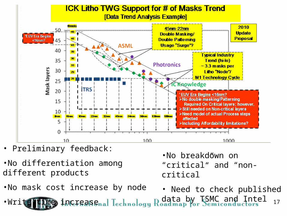
17
• Preliminary feedback:
•No differentiation among different products
•No mask cost increase by node
•Write time increase
•No breakdown on “critical” and “non-critical”
• Need to check published data by TSMC and Intel

18
Some 2011 Update Focus• Potential Solutions (long term vs short term)• Number of masks trend• Impact of LWR on EUV mask inspection. • EUV blank surface roughness is not in the spec (actinic and
non actinic inspection) • Imprint LER Litho resist spec• DSA – Start a new table OR become part of double
patterning• Computational Lithography – Start a new table OR figures• Data Volume for mask and maskless writers update• Max in mask write time (for process control and throughput )• Mask Grid – 0.5nm (0.125nm 1X) or 0.4nm (0.1nm 1X)?
19
Summary• Lithography solutions for 2010
– 45 nm half-pitch - 193 Immersion Single Exposure for DRAM/MPU
– Flash using Double Patterning (Spacer) for 32 nm half-pitch
• Lithography solutions for 2013– 32 nm half-pitch Double patterning or EUV for DRAM/MPU– EUV needed – 16 nm half-pitch for Flash and 22nm
DRAM/MPU
• Double exposure / patterning requires a complex set of parameters when different exposures are used to define single features
• Mask Complexity for Double patterning• Mask Infrastructure for EUV


![ITRS 2001 Renewal - Work in Progress - Do Not Publish 1 [Per IRC Approved Proposals 3/27/01, Scenario 2.0/3.7] ITRS IRC/ITWG Meeting ORTC Proposal Review.](https://static.documents.pub/doc/80x56/55149715550346f06e8b5550/itrs-2001-renewal-work-in-progress-do-not-publish-1-per-irc-approved-proposals-32701-scenario-2037-itrs-ircitwg-meeting-ortc-proposal-review.jpg)
