1 Stability Enhancement Module for Grid-Following Converters: Hardware Implementation and Validation Yin Li, Lingling Fan, Yi Zhou, Zhixin Miao Department of Electrical Engineering, University of South Florida Tampa FL USA 33620 Corresponding author: Lingling Fan, [email protected]Abstract Low-frequency oscillations limit power delivery of voltage-source converter (VSC) interfaced resources, e.g., wind and solar, operating in grid-following control mode. Our prior research identified the instability mechanism as the coupling between real power and voltage at point of common coupling (PCC). In turn, a stability enhancement control was proposed to weaken the coupling by introducing a simple voltage-based feedback loop. The stability enhancement control has been validated via electromagnetic transient (EMT) simulation testbeds. The objectives of this paper are (i) to provide a more insightful explanation of the enhancement module by examining the impedance of the grid-following converter, and (ii) to verify the performance of the stability module using a hardware testbed. The theoretic examination demonstrates that stability enhancement module effectively reduces the negative resistance effect of Z qq and thus boosts stability. The experimental research leads to a hardware testbed of a grid-following converter with the ability of demonstrating low-frequency oscillations. The experimental results demonstrate the efficacy of the proposed stability enhancement control and the readiness of commercial realization of the stability enhancement unit. Index Terms Stability control; vector control; voltage-source converters; impedance; hardware; sbRIO. I. I NTRODUCTION W EAK grid interconnection has been identified by North American Electric Reliability Corporation (NERC) as a major operation challenge for inverter-based resources (IBR) [1], [2]. Low-frequency oscillations have been observed in real-world wind farms in Texas [3], [4] (4 Hz) and solar farms [5] (7 Hz) due to voltage source converter (VSC) operating in a system with low short circuit ratio (SCR). The goal of this paper is to present mechanism and hardware experiment validation results of a stability enhancement module for grid-following converters to operate in weak grids. A. Literature review There are existing works on analysis and control design related to grid-following VSCs for stability enhancement in weak grids, e.g., [6]–[14]. While all the papers addressing stability issues associated with grid-following VSC in weak grids, the major influencing factors on instability identified from those papers are different. In turn, the enhancement design proposals are also different. Roughly speaking, the research works can be classified into two categories: • those that view phase-locked-loop (PLL) dynamics as the major influencing factor [6]–[11], [15], [16]; and • those that view outer control as the major influencing factor, [12]–[14], [17], [18], [19], [20]. It can be seen that the first category research views PLL dynamics play a big role. In turn, tuning parameters of PLL to increase PLL bandwidth is one mitigation for stability enhancement, e.g., [6], [7]. Or a part of the vector Y. Li, L. Fan, Y. Zhou, and Z. Miao are with the Department of Electrical Engineering, University of South Florida, Tampa, FL 33620 USA e-mail: [email protected].
Transcript
1
Stability Enhancement Module for Grid-FollowingConverters: Hardware Implementation and
ValidationYin Li, Lingling Fan, Yi Zhou, Zhixin Miao
Department of Electrical Engineering, University of South FloridaTampa FL USA 33620
Low-frequency oscillations limit power delivery of voltage-source converter (VSC) interfaced resources, e.g.,wind and solar, operating in grid-following control mode. Our prior research identified the instability mechanism asthe coupling between real power and voltage at point of common coupling (PCC). In turn, a stability enhancementcontrol was proposed to weaken the coupling by introducing a simple voltage-based feedback loop. The stabilityenhancement control has been validated via electromagnetic transient (EMT) simulation testbeds. The objectives ofthis paper are (i) to provide a more insightful explanation of the enhancement module by examining the impedanceof the grid-following converter, and (ii) to verify the performance of the stability module using a hardware testbed.The theoretic examination demonstrates that stability enhancement module effectively reduces the negative resistanceeffect of Zqq and thus boosts stability. The experimental research leads to a hardware testbed of a grid-followingconverter with the ability of demonstrating low-frequency oscillations. The experimental results demonstrate theefficacy of the proposed stability enhancement control and the readiness of commercial realization of the stabilityenhancement unit.
WEAK grid interconnection has been identified by North American Electric Reliability Corporation (NERC) asa major operation challenge for inverter-based resources (IBR) [1], [2]. Low-frequency oscillations have been
observed in real-world wind farms in Texas [3], [4] (4 Hz) and solar farms [5] (7 Hz) due to voltage source converter(VSC) operating in a system with low short circuit ratio (SCR). The goal of this paper is to present mechanism andhardware experiment validation results of a stability enhancement module for grid-following converters to operatein weak grids.
A. Literature review
There are existing works on analysis and control design related to grid-following VSCs for stability enhancementin weak grids, e.g., [6]–[14]. While all the papers addressing stability issues associated with grid-following VSCin weak grids, the major influencing factors on instability identified from those papers are different. In turn, theenhancement design proposals are also different.
Roughly speaking, the research works can be classified into two categories:• those that view phase-locked-loop (PLL) dynamics as the major influencing factor [6]–[11], [15], [16]; and• those that view outer control as the major influencing factor, [12]–[14], [17], [18], [19], [20].It can be seen that the first category research views PLL dynamics play a big role. In turn, tuning parameters of
PLL to increase PLL bandwidth is one mitigation for stability enhancement, e.g., [6], [7]. Or a part of the vector
Y. Li, L. Fan, Y. Zhou, and Z. Miao are with the Department of Electrical Engineering, University of South Florida, Tampa, FL 33620USA e-mail: [email protected].
2
control components is redesigned to enhance performance associated to PLL. For example, [8], [9] suggest to havePLL’s input taken from a bus closer to the grid, instead of the PCC bus. In [10], the inner loop is redesignedto have a frequency-based damping block included. In [11], the inner loop has supplementary modulation blocksadded to modulate the PLL angle and the converter voltages. dq-axis current errors are used as the feedback signalsfor the modulation blocks. To avoid the negative effect from PLL in the weak grid, [15] and [16] propose thealternative control strategies which do not require the PLL for the synchronization. [15] proposes a unified virtualsynchronous control which can make the VSC emulate the rotor behavior of a synchronous generator to realizegrid synchronization. The control strategy for the VSC in [16] is the direct power control and it omits the innercurrent loop and PLL. Our prior research in [21] indicates that PLL does influence stability, a finding documentedin [6], [7]. On the other hand, even when PLL parameters are well tuned, low-frequency oscillations may occurdue to outer control and weak grid condition.
In the second category research, our prior research finding [17], [18] aligns with the research findings in Strachanand Jovcic’s 2010 paper [12] and the rest of the papers in the second category [13], [14], [19], [20]. These papersview outer loops playing a big role in low-frequency oscillation stability. To enhance stability, [12] tunes ac voltagecontrol parameters; and [14] redesigned ac voltage control. In [13], a supplementary module is designed to modulateouter loop control command signals. The modulation block is to introduce the decoupling effect and overcome non-linearity. The added control employs gain scheduling technique. Under different operation conditions, gains shouldbe calculated respectively. [19] adds a feedforward part in PLL to mitigate the coupling between PLL dynamicsand grid impedance. [20] claims that the feedforward of PCC voltage can suppress the grid current harmonics butit also suffers from poor stability in weak grid. The authors use the grid voltage as the feedforward in the vectorcontrol instead of the PCC voltage.
B. Objectives of this paper
The goal of this research is to provide a simple and easy to implement control patch to enhance the performanceof an existing VSC with grid-following vector control. Thus, we seek supplementary control. The overall objectiveof our research is similar as that of [13]: to provide a supplementary module to an existing grid-following control.
Our prior research [17] has identified the instability mechanism as the coupling between the real power andvoltage at point of common coupling (PCC). In turn, a stability enhancement control was proposed to weaken thecoupling by introducing a simple feedback control [18]. The output of the enhancement control modulates the powerorder of the grid-following control with the PCC voltage deviation as input. The stability enhancement control hasbeen validated via EMT simulation testbeds in [18].
P
Q
Grid
PCC
Figure 1: The simplified topology of grid-integrated wind energy system.
Fig. 1 presents a circuit diagram of a grid-integrated wind energy system. The grid connected converter regulatesreal power and PCC voltage control. Transmission grid is represented as a pure reactance. Fig. 2(a) presents asimplified linear model of a grid-interconnected VSC system developed in [17] and Fig. 2(b) presents the conceptualdesign of stability enhancement module developed in [18]. The linear model in Fig. 2 assumes PCC voltage orientedvector outer loop control and ignores phase-locked-look (PLL), VSC inner current control loop, and transmissionline electromagnetic dynamics.
It has been presented in [18] that the out most loop from ∆VPCC to ∆P2, and further through converter controlto ∆id causes instability. Thus, introducing a feedback loop with the PCC voltage deviation ∆VPCC as input tomodulate the power order is equivalent to reducing the coupling between ∆VPCC to ∆P2. In turn, stability can beimproved.
The first objective of this paper is to examine the mechanism of voltage feedback loop on stability enhancementusing an alternative approach, While our previous research relies on classical single-input single-output controlsystem diagram and demonstrates that the voltage feedback loop weakens the coupling between power and voltage,
3
Grid
PCC
abc/dq
vd
vqPI
Dω
ω0
++ q PLL
vabc
ω
P
Q
Vpcc V¥jXg
Diq*
Did* Did
Kpp+Kip/s+DP
*
DP
-
-DV*
+ DVPCC
Kpv+Kiv/s
1
1+ti s
Diq1
1+ti s-Xg
DVPCC+
+id
VPCC
G(s)
-c+
+
Did*
DidKpp+Kip/s
+DP*
DP
-1
1+ti s
DVpccid
Vpcc
-c
++
G(s)
x
Did* Did
Kpp+Kip/s+DP
* -1
1+ti s
DVpcc
id-c G(s)
Vpcc-
DP1
DP2
DP1
DP2
x
No control
(a)
(b)
DP1
DP2
(a)
Did*
DidKpp+Kip/s
+DP* -1
1+tisDVPCC
id
VPCC
-c
+
+
G(s)
DP1
DP2
Kid
+
Kid
-
Did* Did
Kpp+Kip/s+
DP*-
1
1+tis
DVPCC
id-c G(s)
VPCC-
DP1
DP2
Kv
+
Kv
-
(a)
(b)(b)
Figure 2: Linear system block diagram and conceptual design of the stability enhancement control. The diagram in (b) is obtained afterreorganizing the diagram in (a).
an examination using equivalent impedance will be conducted in this paper to provide a more direct explanation. Ithas to be noted that dq-frame impedance of a grid-following converter has been examined in the literature, e.g., [6],[22], [23]. Characteristics of impedance can provide insights on system stability. For example, [23] demonstratesthat qq-component impedance (Zqq) is a negative resistor due to synchronization, which may cause stability issues.In this paper, we aim to demonstrate if the enhancement unit can mitigate the negative resistor effect of Zqq.
The second objective is to implement the stability enhancement module in hardware. This research will not onlyprovide validation of the proposed stability enhancement control via hardware, but also provide a feasible approachof testbed building and control implementation to allow fellow researchers to validate analysis results and conductcontrol prototyping.
A hardware testbed of a grid-interfaced converter with the ability of demonstrating low-frequency oscillationshas not been seen in the literature. Among those references in Section I.B, only [15], [16], [19], [20] validate theproposed control systems using hardware testbeds. [15], [16] actually use the control hardware-in-the-loop (CHIL)testbed for the validation and there is no physical circuit and IGBT-based inverter employed. So their real-timeresults do not include the physical dynamics from the IGBTs and LC components. [19], [20] implement controlson the hardware testbed. Their research scopes and experiment results focus on high-frequency harmonics ratherthan the low-frequency oscillations.
Similarly, in the following two frequently-cited articles, [22], [24], where hardware experiments have beenconducted for grid-interconnected VSC, the dynamics investigated focus on oscillations with frequency greaterthan 60 Hz. Low-frequency oscillations with frequency less than 10 Hz have not been replicated.
A major challenge in hardware test is how to replicate low-frequency oscillations. This requires a completeimplementation of VSC vector control and a VSC operating at a high power level. In this paper, this challenge istackled. The designed testbed can be used for stability investigation related to grid-interconnected VSC systems.Applications can extend not only to stability issues in solar/wind grid integration or VSC-HVDC systems, but alsoto recent observed oscillation issues in data center grid connection systems [25], and electric railway systems [26].
In summary, our contribution is two-fold.• The mechanism of the stability enhancement module is revealed as reducing the magnitude of the qq-component
of the converter impedance which behaves as a negative resistor. This is achieved by reducing the dd-axisadmittance through the stability enhancement module.
• Stability enhancement module is realized in hardware implementation and shown efficacy in improving stability.
4
Our proposed stability enhancement module is to decouple a VSC’s real power export and the PCC voltage,or to reduce the sensitivity of power export against the PCC voltage. The modulation block is a simplefeedback control block with the PCC voltage deviation as the input and the output modulates the power order.Compared to the proposed stability enhancement module in [13], the proposed module is much simpler andeasy to implement.
The remainder of the paper is organized as the follows. Section II presents an examination of the effect ofthe enhancement module on converter admittance and impedance. Section III presents the configuration of thelaboratory testbed and vector control hardware implementation. Section IV presents stability enhancement. SectionV concludes the paper.
II. EFFECT OF STABILITY MODULE ON CONVERTER’S EQUIVALENT IMPEDANCE
Impedance-based models can give a very direct measure regarding a component’s passivity. Generally speaking,if in a system, all components are passive (every component has positive resistance in all frequency range), thesystem is stable. On the other hand, non-passivity indicates a potential issue in stability [27], [28].
Reference [23] has noted an important feature of grid-following converter: the qq-component of the incrementalimpedance (Zqq) behaves as a negative resistor. This feature is due to synchronization and has been used to explaininstability issue in [23]. In this section, we aim to demonstrate the effect of the stability enhancement module onthe equivalent negative resistor.
First, relying on the quasi steady-state condition, effect of stability enhancement module on Ydd is examined.Next, relying on the analytical models built in [18] which includes full dynamics details, the admittance model andthe impedance model are extracted and Bode plots are presented to confirm that stability module indeed makes thenegative resistor in Zqq much smaller.
A. Effect on YddIn a dq-frame, the real power and its small-disturbance expression can be expressed as follows.
P = vdid + vqiq
∆P = id∆vd + vd∆id + iq∆vq + vq∆iq (1)
The vector control is based on a dq-frame with the d-axis aligned to the PCC voltage and the q-axis leads thed-axis by 90 degree; thus, at steady state, vd = VPCC and vq = 0 where VPCC is the PCC voltage magnitude. (1)becomes the following:
P = VPCCid, Q = −VPCCiq (2)
∆P = id∆vd + vd∆id + iq∆vq (3)
The dq-domain admittance matrix relates the dq-frame PCC voltage and exporting current in the frequencydomain as follows. [
∆id∆iq
]= −
[Ydd YdqYqd Yqq
] [∆vd∆vq
](4)
Substituting ∆id by −(Ydd∆vd + Ydq∆vq) in (3) leads to the following:
∆P = (id − Yddvd)∆vd + (iq − Ydqvd)∆vq (5)
In the frequency domain, the low-frequency range may represent the quasi steady-state operating condition ofthe system. Thus, we may assume that ∆P = 0 for constant power control at the low-frequency range. Thebandwidths of the real power control and the ac voltage control are usually different. Voltage control is usually setslightly faster than the power control. Hence, we may assume even when the voltage experiences disturbances, i.e.,∆VPCC = ∆vd 6= 0, the power keeps constant at very low-frequency range (∆P = 0).
With the above assumption, (5) becomes the following:
0 = (id − Yddvd)∆vd + (iq − Ydqvd)∆vq (6)
5
Hence,
Ydd =idvd
=P
VPCC2 (7)
Ydq =iqvd
= − Q
VPCC2 (8)
It can be see that Ydd is resistive at steady-state. The magnitude of Ydd becomes greater when the real powerlevel increases or the PCC voltage magnitude reduces.
The stability enhancement module modifies the power order as ∆P ∗ = Kv∆VPCC = Kv∆vd. At steady-state,real power P tracks P ∗. Hence, the following relationship exists:
Kv∆vd = (id − Yddvd)∆vd + (iq − Ydqvd)∆vq. (9)
The above relationship exists for any ∆vd or ∆vq under the following condition:
Ydd =id −Kv
vd(10)
Ydq =iqvd
(11)
Thus, we can see that introducing the voltage feedback, with the gain Kv < id, can effectively decrease theequivalent Ydd of the converter. On the other hand, it does not change Ydq.
B. Admittance model and impedance model
Since impedance is the inverse of admittance, reduction in Ydd will influence mostly on Zqq. This point isconfirmed using the admittance model extracted from the dq-frame analytical model built in [18]. The analyticalmodel represents a measurement testbed where the PCC bus is connected to the measurement point by a verysmall impedance (Rg = 0.001 pu and Xg = 0.01 pu). The VSC controller parameters are same as those in Fig. 9.The VSC’s power exporting level is 0.75 pu and the PCC voltage is controlled at 1 pu. The measurement point isconnected to a 60 Hz voltage source for steady operation. By perturbing the dq-axis voltage source and treating thecurrent into the converter as the output, the input/output model, or the admittance model Y is obtained. Further, Zis obtained by inverting Y .Y1 and Z1 represent the admittance and impedance without stability module. The stability module is implemented
with two gains: Kv at 0.5 and 0.7. The resulting admittances and impedances are Y2/Z2 for Kv = 0.5 and Y3/Z3
for Kv = 0.7. Fig. 3 confirms that stability module has negligible influence on the rest three components, whileit has a major influence on Ydd. The magnitude of Ydd at 0.2 Hz reduces from 0.7 pu to 0.25 pu or 0.06 pu,respectively for the two gains.
Fig. 4 confirms that Zqq behaves as a negative resistor and the stability module reduces the magnitude of Zqq
for the entire frequency range from 0.1 Hz to 1000 Hz. The effect of reduction is most obvious at frequency lessthan 10 Hz.
Remarks: Both analysis and numerical results show that the stability enhancement module effectively reducesYdd and the magnitude of Zqq. Since Zqq behaves as a negative resistance, the stability enhancement model thusreduces the effect of negative resistance and improves VSC’s passivity.
III. CONFIGURATION OF LABORATORY TESTBED
A. Circuit
Compared to software simulation, a hardware testbed provides realistic implementation of controllers and high-fidelity validation. To validate the performance of the stability control, a laboratory hardware testbed is built,consisting of a grid-connected VSC with vector control. The topology of the test system is shown in Fig. 5.
The test system represents a converter in a weak grid. The converter is connected to the PCC bus through achoke. From the PCC bus, the grid is viewed as a Thevenin equivalent: a constant voltage behind an inductivesource impedance. In addition, since many wind farms or solar farms employ shunt compensation, we also put
6
−40
−20
0From: In(1)
To: O
ut(
1)
−180
0
180
To: O
ut(
1)
−50
0
50
To: O
ut(
2)
10−1
100
101
102
103
−180
0
180
To: O
ut(
2)
From: In(2)
10−1
100
101
102
103
Bode Diagram
Frequency (Hz)
Magnitude (
dB
) ; P
hase (
deg) Y1
Y2
Y3
Figure 3: Bode plots of the admittance. Y1: no stability module. Y2 and Y3: with stability module, Kv at 0.5 and 0.7 respectively. Stabilitymodule mainly changes Ydd.
−50
0
50From: In(1)
To: O
ut(
1)
−180
−90
0
90
180
To: O
ut(
1)
−50
0
50
To: O
ut(
2)
10−1
100
101
102
103
−180
0
180
To: O
ut(
2)
From: In(2)
10−1
100
101
102
103
Bode Diagram
Frequency (Hz)
Magnitude (
dB
) ; P
hase (
deg)
Z1
Z2
Z3
Figure 4: Bode plots of the impedance. Z1: no stability module. Z2 and Z3: with stability module, Kv at 0.5 and 0.7 respectively. Stabilitymodule mainly changes Zqq .
shunt capacitors into the circuit to represent shunt compensation. The choke and the shunt capacitor serve as anLC filter.
The VSC includes a dc voltage source connected to a three-phase DC/AC inverter. The three-phase DC/ACinverter are a two-level VSC and it contains two IGBTs on each phase. The PWM signals for the inverter aregenerated by a field-programmable gate array (FPGA)-based controller. All devices and components are at thelaboratory scale.
The system comprises of three single-phase LC filters and three single-phase inductive transmission lines. TheLC filters between the converter and the PCC bus are used to to filter out harmonics generated by the inverter. Asingle-phase LC filter contains four inductors, one capacitor (47 µF), and the resistance of each wire (0.5 Ω). Thefour 5.6 mH inductors are connected as shown in Fig. 5 to double the current handling capacity of the filter. Thetotal inductance of each filter (L1) remains at 5.6 mH. The PCC bus and the grid are connected via a transmissionline. In the hardware testbed, the transmission line is represented by multiple identical inductors connected in series.
7
Vg =14.7 V (L-L)
LR
Rg = 2R
+
-
+
-
Vdc=40 V
L
L L
L1 = L
L L L
6L Lg 8L
R R
LR
L
L LL L L R R
LR
L
L LL L L R R
C C C
P*
V*Vector Control
iabc vpc c,abc
PWM
ia
ib
ic
vpc c,a
vpcc,b
vpc c,c
R = 0.5 Ω
L = 5.6 mH
C = 47 μF
R1 = R
Figure 5: The topology of the hardware testbed with the control system.
Hence, the length of the transmission lines can be determined by the number of inductors and the total inductanceis represented by Lg. The resistance of the transmission line (Rg) is from the wires used for connection. Theparameters used in the hardware testbed and the corresponding per-unit (pu) values are listed in Appendix Table I.
X1=0.195 pu
B1=0.19 pu
VSC
P*
V*Vector Control
iabc vpc c,abc
PWM
+
-Vdc
Vg = 1 puR1=0.046 pu
Sbase = 20 VA
Vbase = 14.7 V
Rg=0.09 pu
1.17 pu 1.56 puXgXg
VPCC
Figure 6: The topology of the grid-connected VSC system with circuit parameters in pu, which corresponding to Fig. 5.
For analysis and control design, per-unit values are preferred. Based on the current and voltage limits of thedevices and the components, power base Sbase is selected as 20 VA while voltage base Vbase is 14.7 V. The single-line diagram of the above system is shown in Fig. 6 with per-unit values. X1 and Xg represent the reactance inpu after aggregation of multiple inductors. R1 and Rg are also in pu. B1 indicates how much reactive power in puis generated by the three-phase capacitors.
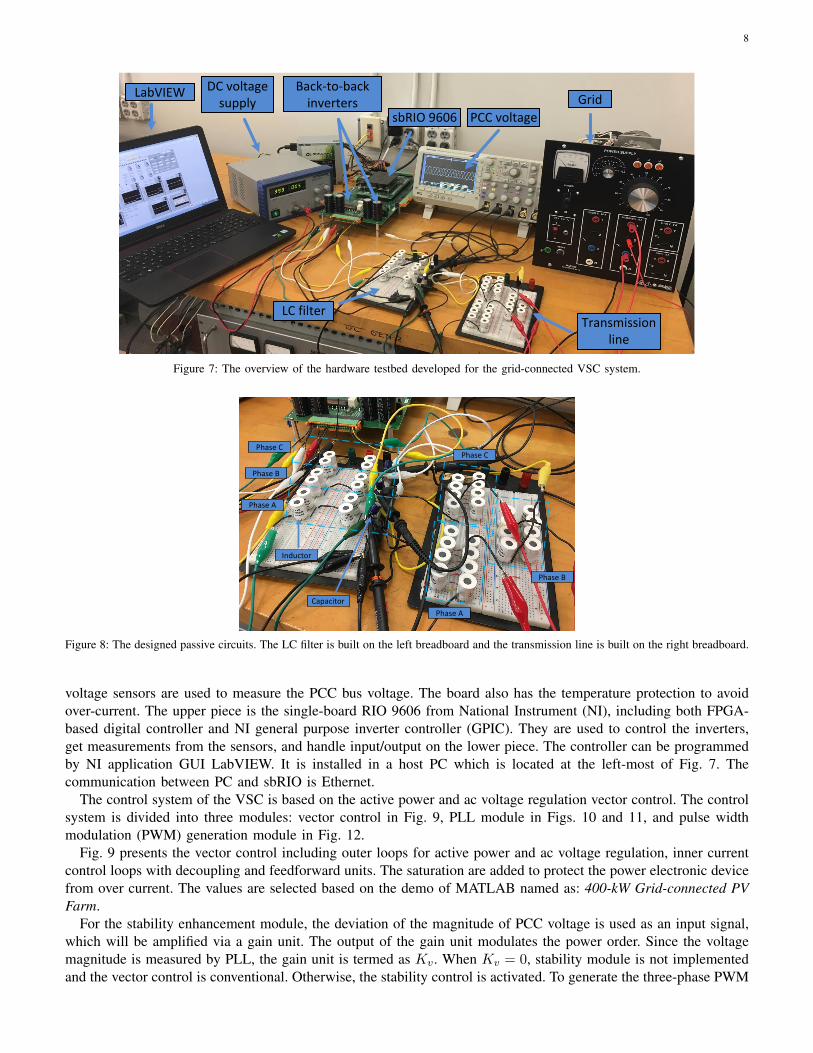
Fig. 7 is the picture of the physical hardware testbed built. All of devices in this picture are labeled by the namescorresponding to elements in Fig. 5. The dc voltage supply used is BK Precision 1666 with voltage range of 0−42V and power rating at 200 W. It supplies 40 V voltage at the DC side of the inverter. The grid is emulated by abalanced three-phase 60-Hz AC voltage source (Lab-Volt 8821-20). Its voltage range is 0− 120 V and maximumcurrent is 5 A. Lab-Volt 8821-20 converts 208 V grid voltage to 14.7 V. Two passive circuits are designed on thebreadboards: the LC filter and the inductive transmission line respectively. Fig. 8 shows the details and the dashedblue lines circled the elements on each phase.
B. Vector control implementation
A three-phase back-to-back inverter research board is used to configure a VSC. This board includes three pieces.The lower piece is named as mini-scale SKiiP3 Replica Back-to-Back Converter. It contains two embedded inverters(A and B). We used Inverter A as the VSC in the testbed. Each inverter has three-phase voltage sensors and three-phase current sensors at converter side. The current sensors are used to measure the converter currents while the
8
LabVIEW DC voltage supply Grid
Transmission line
LC filter
Back-to-back inverters
sbRIO 9606 PCC voltage
Figure 7: The overview of the hardware testbed developed for the grid-connected VSC system.
Capacitor
Phase A
Phase B
Phase C
Phase A
Phase B
Phase C
Inductor
Figure 8: The designed passive circuits. The LC filter is built on the left breadboard and the transmission line is built on the right breadboard.
voltage sensors are used to measure the PCC bus voltage. The board also has the temperature protection to avoidover-current. The upper piece is the single-board RIO 9606 from National Instrument (NI), including both FPGA-based digital controller and NI general purpose inverter controller (GPIC). They are used to control the inverters,get measurements from the sensors, and handle input/output on the lower piece. The controller can be programmedby NI application GUI LabVIEW. It is installed in a host PC which is located at the left-most of Fig. 7. Thecommunication between PC and sbRIO is Ethernet.
The control system of the VSC is based on the active power and ac voltage regulation vector control. The controlsystem is divided into three modules: vector control in Fig. 9, PLL module in Figs. 10 and 11, and pulse widthmodulation (PWM) generation module in Fig. 12.
Fig. 9 presents the vector control including outer loops for active power and ac voltage regulation, inner currentcontrol loops with decoupling and feedforward units. The saturation are added to protect the power electronic devicefrom over current. The values are selected based on the demo of MATLAB named as: 400-kW Grid-connected PVFarm.
For the stability enhancement module, the deviation of the magnitude of PCC voltage is used as an input signal,which will be amplified via a gain unit. The output of the gain unit modulates the power order. Since the voltagemagnitude is measured by PLL, the gain unit is termed as Kv. When Kv = 0, stability module is not implementedand the vector control is conventional. Otherwise, the stability control is activated. To generate the three-phase PWM
9
vtq+-
+-
id*
+
+
-
ud
uq
0.195
+
dq
abc
vtd
vt,abc
0.4+40/s+
-
-
VPCC
V*
0.195
0.4+4/s
0.4+4/s++
P
P*
id
iq
iq*
vd
+
ΔVPCC
Kv ΔVPCC
+vq
2Vbase
3
mabc
max=1
min=-1
0.2+20/s
min=-1
max=1
max=2
min=-2
max=2
min=-2
cos(q ) sin(q )
2
Vdc
Figure 9: The vector control with the stability enhancement module which is shown in the blue dashed box.
modulation signal mabc, the terminal voltage vt is converted first from dq frame to abc frame, then to physical unitby multiplying
√2Vbase√
3, and finally dividing Vdc
2 .The PLL module synchronizes all of measurements with the PCC voltage and converts them from abc frame to
dq frame. The readings from the voltage and current sensors are in physical units, va, vb, vc, ia, ib, and ic. Invertervoltage sensors are used to measure the three-phase PCC voltage while the inverter current sensors are used tomeasure the converter current. Before any calculation and frame transformation, all of required measurements needto be converted to pu values, as shown in Fig. 10. E.g., vpcc.abc and iabc are all in pu. The scaling gains are√
3√2Vbase
and√3Vbase√2Sbase
for the voltage and current respectively. Fig. 11 shows the detailed structure of a second-ordersynchronous reference frame PLL implemented in the testbed.
The two synchronization signals cos(θ) and sin(θ) generated by PLL are used for Park transformation. In thiscontrol system, the dq-frame assumes q leading d, or d+jq. After obtaining the dq components of the PCC voltageand converter current, we may use them to calculate the power measurement and the magnitude of PCC voltage.
abc
dq
Vu_B
Vbase
3
2Vv_B
Vw_B
vpcc,abc
PLL
f
sin(q )
cos(q )
sin(q )
cos(q )
vpcc,abc vd
vq
Iu_A
Sbase2Iv_A
Iw_A
i1,abcVbase3
abc
dq
iabc id
iq
vd
vq
id
iq
vdid+vqiq P
Qvqid+vdiq
vd2+vq
2VPCC
sin(q )
cos(q )
Figure 10: The modules used in the LabVIEW model for PLL and frame transformations.
Fig. 12 shows the PWM module which generates gate signals and sends them to the switches of Inverter Adirectly. The module for PMW-signal generator is FPGA-based and it uses the clock of FPGA controller at 40
10
abc
dq
sin(q )cos(q )
vpcc,abc
vd
vq60+1400/s 1/s
Δω+
ω0
+q
cos()
sin()
Figure 11: The control schematics of the PLL.
MHz. The three-phase modulation signals mabc are generated from vector control (shown in Fig. 9) and the carrierfrequency is set at 4 kHz. Hence, the IGBT switching is at 4 kHz.
mabc
Triangle Gen
fc = 4 kHz
mb
ma
mc
uTOPAuBOTAvTOPAvBOTAwTOPAwBOTA
switches
Figure 12: 40 MHz FPGA-based module of PWM-signal generator developed in the LabVIEW model.
C. Experiment results for conventional vector control
We implement the above vector control in the hardware testbed and test its performance. The control parametersused in the hardware testbed are same as those in Fig. 9. The system performance upon a step change in powertransfer order is examined. The six-inductors transmission line was used, i.e., Xg = 1.17 pu. The dynamic responsesof real power generated by VSC, converter current in d-axis, and PCC voltage magnitude were monitored. Theexperimental results were plotted by MATLAB using the data exported from LabVIEW GUI.
To find the power transfer capability of this VSC-based system, the power reference was increased from 0.2 puto a higher power conditions at 5 sec. The marginal condition happened when P ∗ was increased from 0.2 pu to0.65 pu. Two conditions of P ∗ = 0.60 and P ∗ = 0.65 pu were selected and the corresponding experiment resultswere plotted in Fig. 13. The blue lines represent the measurements corresponding to P = 0.60 pu while the redlines are for the case of P = 0.65 pu. It is observed that the system returned to stability after the power order wasincreased to 0.60 pu while it became unstable after the power order was increased to 0.65 pu. Based on Fig. 13,the oscillation frequency is 3.8 Hz and a power exporting level of 0.65 pu is the marginal condition.
The oscilloscope was used to monitor the three-phase instantaneous voltages at PCC bus. Fig. 14 shows thetransient dynamics of VPCC when the power transfer level was changed from 0.2 pu to 0.65 pu. It was observedthat low-frequency oscillations happened in VPCC.
IV. STABILITY ENHANCEMENT
According to [18], there are two ways to reduce the coupling between PCC voltage and real power. Both methodsprovide modulation to the real power order. The first method is to feedback the PCC voltage deviation ∆VPCC. Theother one is to feedback the d-axis of converter current deviation ∆id. It has been investigated in [18] that voltagefeedback has a much better performance compared to the current feedback control. Hence, this paper focuses onvoltage feedback stability enhancement.
The stability control was implemented in the hardware testbed. The feedback part is shown in the dashed box inFig. 9. It can be activated by assigning a non-zero value to Kv. In this section, besides P , id, and VPCC, we alsomonitor the value of feedback gain Kv and the output from the feedback control.
11
4 6 8 10 12 14
P (
pu)
0
0.5
1
4 6 8 10 12 14
i d (
pu)
0
0.5
1
time (s)4 6 8 10 12 14
VP
CC
(pu)
0.5
1
1.5
Figure 13: With the conventional control and the six-inductors transmission line (Xg=1.17 pu), the transferred power level of the systemwas increased from 0.2 pu to 0.60 pu (red lines) and 0.65 pu (blue lines).
(a) (b)
Figure 14: Three-phase PCC voltage shown in oscilloscope for the system with the conventional control and the six-inductors transmissionline (Xg=1.17 pu). (14a): PCC voltages showed the instability after P was increased from 0.2 pu to 0.65 pu. (14b): zoom in to show thedetails.
A. Six-inductors transmission line
Selecting the best value for Kv has been discussed in [18]. It is indicated that the best value of Kv is equal tothe power transfer level for a complete power and voltage decoupling. The value of the gain Kv is selected to bethe same as P ∗.
The power transfer level was increased from 0.2 pu to 0.65 pu at 5 sec and the stability control was activated at10 sec by assigning values to Kv. In Fig. 15, Kv is assigned to be equal to P ∗. The stability control with Kv = P ∗
stabilizes the system after it was activated at 10 sec.To find how much the stability control with Kv = P ∗ can improve the system power exporting capability, the
power transfer level was kept increasing. It was found that when P ∗ was increased to 0.72 pu, the system keptstable. However, when P ∗ was increased from 0.2 pu to 0.75 pu, the system lost the stability with the oscillationsaround 7.5 Hz. Fig. 16 presents the aforementioned dynamics of the system. The power transfer level was increasedat 5 sec. The blue lines represent the measurements corresponding to P ∗ = 0.72 pu while the red lines are relatedto the case of P ∗ = 0.75 pu. Comparing Fig. 13 and Fig. 16, it can be found that the stability enhancement withKv = P ∗ can improve the power capability of the system by 15%.
Remarks: The hardware implementation shows that the voltage feedback stability control can enhance stabilitymargin by 15%. Compared to the analytical model, the hardware testbed presents more noise caused by the switchingdynamics and the sensors. A larger gain Kv may bring more noise from the voltage measurement to the powerorder, which in turn may reduce the performance of the stability control.
B. Eight-inductors transmission line
The stability control was also tested for a longer transmission line. In this subsection, the length of transmissionline was increased by adding two more inductors. In another words, Xg was increased from 1.17 pu to 1.56 pu.Through eight-inductors transmission line, the power transfer level P ∗ of the system with the conventional control
12
4 6 8 10 12 14
Kv
0
0.5
1
4 6 8 10 12 14P
(p
u)
0
0.5
1
4 6 8 10 12 14
i d (
pu
)
0
0.5
1
4 6 8 10 12 14
VP
CC
(p
u)
0.5
1
1.5
time (s)
4 6 8 10 12 14
Co
mp
(p
u)
-0.2
0
0.2
Figure 15: With the six-inductors transmission line (Xg=1.17 pu), the power level was increased from 0.2 pu to 0.65 pu at 5 sec; then, thestability control (Kv = P ∗) was activated at 10 sec. References (red lines); measurements (blue lines).
3 4 5 6 7 8 9 10
Kv
0
0.5
1
3 4 5 6 7 8 9 10
P (
pu
)
0
0.5
1
3 4 5 6 7 8 9 10
i d (
pu
)
0
0.5
1
3 4 5 6 7 8 9 10
VP
CC
(p
u)
0.5
1
1.5
time (s)
3 4 5 6 7 8 9 10
Co
mp
(p
u)
-0.2
0
0.2
Figure 16: With the stability control and six-inductors transmission line (Xg=1.17 pu), the transferred power level of the system wasincreased from 0.20 pu to 0.72 pu (red lines) and 0.75 pu (blue lines).
13
was increased to find the marginal condition. 0.45 pu was found as the marginal condition of the system with theconventional control. The system will be subject to an increase in P ∗ from 0.2 pu to 0.46 pu at 5 sec. Then, thestability control will be activated after 5 seconds by assigning 0.46 to Kv at 10 sec. The experiment results areplotted in Fig. 17. It is observed that the system returned to be stable because the 3.5 Hz oscillation was mitigatedquickly after the stability control was activated.
4 6 8 10 12 14
Kv
0
0.5
1
4 6 8 10 12 14
P (
pu
)
0
0.5
1
4 6 8 10 12 14
i d (
pu
)
0
0.5
1
4 6 8 10 12 14
VP
CC
(p
u)
0.5
1
1.5
time (s)4 6 8 10 12 14
Co
mp
(p
u)
-0.2
0
0.2
Figure 17: With the eight-inductors transmission line (Xg=1.56 pu), the power level was increased from 0.2 pu to 0.46 pu at 5 sec; then,the stability control (Kv = P ∗) was activated at 10 sec. References (red lines); measurements (blue lines).
We kept increasing the power transfer level to check how much the stability control (Kv = P ∗) can improve thesystem capability through eight-inductors transmission line. Fig. 18 presents the experiment results at two conditionswith Kv = P ∗. The red lines indicate that P ∗ was increased from 0.2 pu to 0.6 pu. After the step change at 5 sec,oscillations appeared in the dynamic responses but can be eventually damped out. This means that the system wasapproaching the marginal condition but it is still stable. The blue lines represent the dynamics for the event whenP ∗ increases from 0.2 pu to 0.62 pu. The system becomes unstable due to sustained oscillations.
Remarks: It can be found that 33% more power can be exported for this weak system.
V. CONCLUSION
The conceptual design of the stability control was proposed in our previous work for the grid-following VSCs toenhance weak grid operation. The stability control modulates power order with PCC voltage deviation as feedbacksignal. In this paper, the effect of the stability control on dq-frame impedance is examined and it is found that thecontrol module effectively reduces the negative resistor effect of Zqq. The control is implemented on a laboratoryhardware testbed and the detailed procedures/parameters of the testbed are presented. Although the hardware testbedhas noise in the measurements and process, our design of stability control can lead to good performance. The stabilitycontrol with Kv = P ∗ can improve the stability of VSC-based system stability obviously. For the six-inductorstransmission line (Xg = 1.17 pu) and the eight-inductors transmission line (Xg = 1.56 pu), the transferred powerlevel of the system was increased 15% and 33%, respectively. In addition, the effect of system noise on the controlperformance has been evaluated. The experiment results show that the ripples in power measurements were smallerthan 7% at the steady state even if the stability control was activated. All in all, the performance of the stabilitycontrol has been confirmed by hardware experiments. The practicality of its algorithm and parameters has been
14
3 4 5 6 7 8 9 10
Kv
0
0.5
1
3 4 5 6 7 8 9 10P
(p
u)
0
0.5
1
3 4 5 6 7 8 9 10
i d (
pu
)
0
0.5
1
3 4 5 6 7 8 9 10
VP
CC
(p
u)
0.5
1
1.5
time (s)
3 4 5 6 7 8 9 10
Co
mp
(p
u)
-0.2
0
0.2
Figure 18: With the stability control and the eight-inductors transmission line (Xg=1.56 pu), the transferred power level of the system wasincreased from 0.20 pu to 0.60 pu (red lines) and 0.62 pu (blue lines).
verified by the experimental results. This hardware testbed can be considered as a remarkable achievement oncontrol validation.
DATA AVAILABILITY STATEMENT
Data sharing is not applicable to this article as no new data were created or analyzed in this study.
ACKNOWLEDGEMENT
This project is supported in part by US Department of Energy Solar Energy Technology Office through DE-EE-0008771 grant.
APPENDIX
REFERENCES
[1] (2017, December) Integrating Inverter-Based Resources into Low Short Circuit Strength Systems. NERC.[2] (2018, February) Short-Circuit Modeling and System Strength: White Ppaer. NERC.[3] S. Huang, J. Schmall, J. Conto, J. Adams, Y. Zhang, and C. Carter, “Voltage control challenges on weak grids with high penetration
of wind generation: Ercot experience,” in 2012 IEEE Power and Energy Society General Meeting, July 2012, pp. 1–7.[4] S. H. Huang and G. Yanfeng, Panhandle and South Texas Stability and System Strength Assessment. ERCOT ROS Meeting, March,
2018.[5] First Solar, “Deploying utility-scale pv power plants in weak grids,” 2017 IEEE PES General Meeting, July 2017.[6] L. Harnefors, M. Bongiorno, and S. Lundberg, “Input-admittance calculation and shaping for controlled voltage-source converters,”
IEEE transactions on industrial electronics, vol. 54, no. 6, pp. 3323–3334, 2007.[7] J. Z. Zhou, H. Ding, S. Fan, Y. Zhang, and A. M. Gole, “Impact of short-circuit ratio and phase-locked-loop parameters on the
small-signal behavior of a vsc-hvdc converter,” IEEE Transactions on Power Delivery, vol. 29, no. 5, pp. 2287–2296, 2014.[8] J. A. Suul, S. D’Arco, P. Rodrıguez, and M. Molinas, “Impedance-compensated grid synchronisation for extending the stability range
of weak grids with voltage source converters,” IET Generation, Transmission & Distribution, vol. 10, no. 6, pp. 1315–1326, 2016.[9] M. F. M. Arani and Y. A.-R. I. Mohamed, “Analysis and performance enhancement of vector-controlled vsc in hvdc links connected
to very weak grids,” IEEE Transactions on Power Systems, vol. 32, no. 1, pp. 684–693, 2016.[10] C. Guo, W. Liu, C. Zhao, and R. Iravani, “A frequency-based synchronization approach for the vsc-hvdc station connected to a weak
ac grid,” IEEE Transactions on Power Delivery, vol. 32, no. 3, pp. 1460–1470, 2017.
15
Table I: Parameters of experiment testbed
Parameter Value (SI) Per-unit (pu)Sbase 20 VA 1Vdc 40 VVbase 14.7 V 1ωbase 2π60 rad/s 1
[11] K. Givaki, D. Chen, and L. Xu, “Current error based compensations for vsc current control in weak grid for wind farm applications,”IEEE Trans. Sustain. Energy, pp. 1–1, 2018.
[12] N. P. Strachan and D. Jovcic, “Stability of a variable-speed permanent magnet wind generator with weak ac grids,” IEEE Transactionson Power Delivery, vol. 25, no. 4, pp. 2779–2788, 2010.
[13] A. Egea-Alvarez, S. Fekriasl, F. Hassan, and O. Gomis-Bellmunt, “Advanced vector control for voltage source converters connected toweak grids,” IEEE Trans. Power Syst., vol. 30, no. 6, pp. 3072–3081, Nov 2015.
[14] R. Shah, R. Preece, and M. Barnes, “The impact of voltage regulation of multiinfeed vsc-hvdc on power system stability,” IEEETransactions on Energy Conversion, vol. 33, no. 4, pp. 1614–1627, 2018.
[15] L. Huang, H. Xin, H. Yang, Z. Wang, and H. Xie, “Interconnecting very weak ac systems by multiterminal vsc-hvdc links with aunified virtual synchronous control,” IEEE Journal of Emerging and Selected Topics in Power Electronics, vol. 6, no. 3, pp. 1041–1053,2018.
[16] S. Gao, H. Zhao, Y. Gui, J. Luo, and F. Blaabjerg, “Impedance analysis of voltage source converter using direct power control,” IEEETransactions on Energy Conversion, vol. 36, no. 2, pp. 831–840, 2021.
[17] L. Fan and Z. Miao, “An explanation of oscillations due to wind power plants weak grid interconnection,” IEEE Trans. Sustain. Energy,vol. 9, no. 1, pp. 488–490, Jan 2018.
[18] Y. Li, L. Fan, and Z. Miao, “Stability control for wind in weak grids,” IEEE Trans. Sustain. Energy, vol. 10, no. 4, pp. 2094–2103,Oct 2019.
[19] X. Zhang, D. Xia, Z. Fu, G. Wang, and D. Xu, “An improved feedforward control method considering pll dynamics to improve weakgrid stability of grid-connected inverters,” IEEE Transactions on Industry Applications, vol. 54, no. 5, pp. 5143–5151, 2018.
[20] X. Wang, K. Qin, X. Ruan, D. Pan, Y. He, and F. Liu, “A robust grid-voltage feedforward scheme to improve adaptability of grid-connected inverter to weak grid condition,” IEEE Transactions on Power Electronics, vol. 36, no. 2, pp. 2384–2395, 2021.
[21] L. Fan, “Modeling type-4 wind in weak grids,” IEEE Transactions on Sustainable Energy, vol. 10, no. 2, pp. 853–864, 2019.[22] M. Cespedes and J. Sun, “Impedance modeling and analysis of grid-connected voltage-source converters,” IEEE Transactions on Power
Electronics, vol. 29, no. 3, pp. 1254–1261, 2013.[23] B. Wen, D. Boroyevich, R. Burgos, P. Mattavelli, and Z. Shen, “Analysis of dq small-signal impedance of grid-tied inverters,” IEEE
Transactions on Power Electronics, vol. 31, no. 1, pp. 675–687, 2015.[24] X. Wang, L. Harnefors, and F. Blaabjerg, “Unified impedance model of grid-connected voltage-source converters,” IEEE Trans. Power
Electron., vol. 33, no. 2, pp. 1775–1787, 2017.[25] J. Sun, M. Xu, M. Cespedes, D. Wong, and M. Kauffman, “Modeling and analysis of data center power system stability by impedance
methods,” in 2019 IEEE Energy Conversion Congress and Exposition (ECCE). IEEE, 2019, pp. 107–116.[26] H. Hu, H. Tao, F. Blaabjerg, X. Wang, Z. He, and S. Gao, “Train–network interactions and stability evaluation in high-speed railways–
part i: Phenomena and modeling,” IEEE Trans. Power Electron., vol. 33, no. 6, pp. 4627–4642, 2017.[27] L. Harnefors, X. Wang, A. G. Yepes, and F. Blaabjerg, “Passivity-based stability assessment of grid-connected vscs—an overview,”
IEEE Journal of emerging and selected topics in Power Electronics, vol. 4, no. 1, pp. 116–125, 2015.[28] A. J. Agbemuko, J. L. Dominguez-Garcia, O. Gomis-Bellmunt, and L. Harnefors, “Passivity-based analysis and performance
enhancement of a vector controlled vsc connected to a weak ac grid,” IEEE Transactions on Power Delivery, 2020.