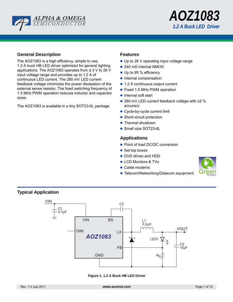
Rev. 1.0 July 2011 www.aosmd.com Page 1 of 12 AOZ1083 1.2 A Buck LED Driver General Description The AOZ1083 is a high efficiency, simple to use, 1.2 A buck HB LED driver optimized for general lighting applications. The AOZ1083 operates from a 3 V to 26 V input voltage range and provides up to 1.2 A of continuous LED current. The 280 mV LED current feedback voltage minimizes the power dissipation of the external sense resistor. The fixed switching frequency of 1.5 MHz PWM operation reduces inductor and capacitor sizes. The AOZ1083 is available in a tiny SOT23-6L package. Features Up to 26 V operating input voltage range 240 mΩ internal NMOS Up to 95 % efficiency Internal compensation 1.2 A continuous output current Fixed 1.5 MHz PWM operation Internal soft start 280 mV LED current feedback voltage with ±5 % accuracy Cycle-by-cycle current limit Short-circuit protection Thermal shutdown Small size SOT23-6L Applications Point of load DC/DC conversion Set top boxes DVD drives and HDD LCD Monitors & TVs Cable modems Telecom/Networking/Datacom equipment Typical Application Figure 1. 1.2 A Buck HB LED Driver LX VIN BS VIN VOUT FB DIM GND C2 10μF C3 C1 4.7μF L1 2.2μH AOZ1083 R S LED1
Transcript
Rev. 1.0 July 2011 www.aosmd.com Page 1 of 12
AOZ10831.2 A Buck LED Driver
General DescriptionThe AOZ1083 is a high efficiency, simple to use, 1.2 A buck HB LED driver optimized for general lighting applications. The AOZ1083 operates from a 3 V to 26 V input voltage range and provides up to 1.2 A of continuous LED current. The 280 mV LED current feedback voltage minimizes the power dissipation of the external sense resistor. The fixed switching frequency of 1.5 MHz PWM operation reduces inductor and capacitor sizes.
The AOZ1083 is available in a tiny SOT23-6L package.
FeaturesUp to 26 V operating input voltage range240 mΩ internal NMOSUp to 95 % efficiencyInternal compensation1.2 A continuous output currentFixed 1.5 MHz PWM operationInternal soft start280 mV LED current feedback voltage with ±5 % accuracyCycle-by-cycle current limitShort-circuit protectionThermal shutdownSmall size SOT23-6L
ApplicationsPoint of load DC/DC conversionSet top boxesDVD drives and HDD LCD Monitors & TVsCable modemsTelecom/Networking/Datacom equipment
Typical Application
Figure 1. 1.2 A Buck HB LED Driver
LX
VIN BS
VIN
VOUT
FB
DIM
GND
C210µF
C3C14.7µF
L1 2.2µH
AOZ1083
RS
LED1
AOZ1083
Rev. 1.0 July 2011 www.aosmd.com Page 2 of 12
Ordering Information
AOS Green Products use reduced levels of Halogens, and are also RoHS compliant.Please visit www.aosmd.com/web/quality/rohs_compliant.jsp for additional information.
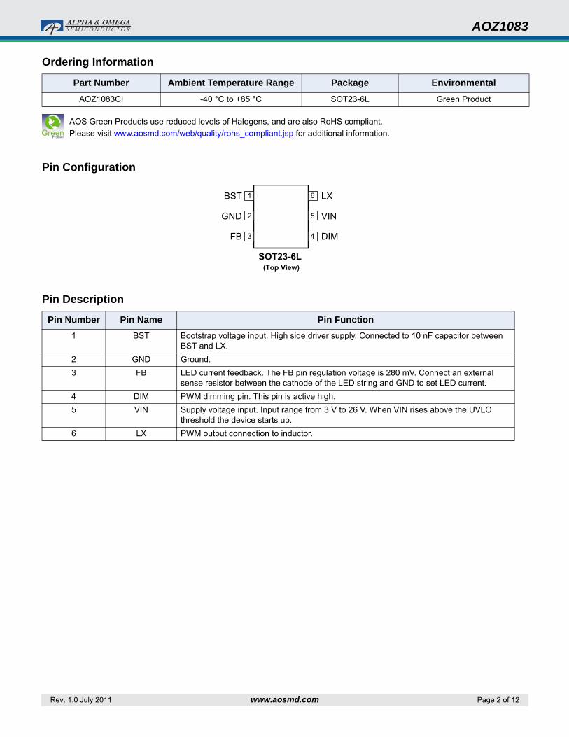
Pin Configuration
Pin Description
Part Number Ambient Temperature Range Package Environmental
AOZ1083CI -40 °C to +85 °C SOT23-6L Green Product
Pin Number Pin Name Pin Function1 BST Bootstrap voltage input. High side driver supply. Connected to 10 nF capacitor between
BST and LX.2 GND Ground.3 FB LED current feedback. The FB pin regulation voltage is 280 mV. Connect an external
sense resistor between the cathode of the LED string and GND to set LED current.4 DIM PWM dimming pin. This pin is active high. 5 VIN Supply voltage input. Input range from 3 V to 26 V. When VIN rises above the UVLO
threshold the device starts up.6 LX PWM output connection to inductor.
LX
VIN
DIM
1
2
3
BST
GND
FB
SOT23-6L (Top View)
6
5
4
AOZ1083
Rev. 1.0 July 2011 www.aosmd.com Page 3 of 12
Absolute Maximum RatingsExceeding the Absolute Maximum Ratings may damage the device.
Note:1. Devices are inherently ESD sensitive, handling precautions are
required. Human body model rating: 1.5 kΩ in series with 100 pF.
Recommended Operating ConditionsThe device is not guaranteed to operate beyond the Recommended Operating Conditions.
Note:2. The value of ΘJA is measured with the device mounted on a 1-in2
FR-4 board with 2 oz. Copper, in a still air environment with TA = 25 °C. The value in any given application depends on the user’s specific board design.
Electrical CharacteristicsTA = 25 °C, VVIN = VDIM = 12 V. Specifications in BOLD indicate a temperature range of -40 °C to +85 °C. These specifications are guaranteed by design.
TSS Soft Start Interval 400 μsPOWER STATE OUTPUTRDS(ON) NMOS On-Resistance VIN = 12 V 240 mΩRDS(ON) NMOS On-Resistance VIN = 3.3 V 380 mΩILEAKAGE NMOS Leakage VDIM = 0 V, VLX = 0 V 10 μA
AOZ1083
Rev. 1.0 July 2011 www.aosmd.com Page 4 of 12
Block Diagram
GND
VIN
DIM
FB
Low VoltageRegulator
DIMDetection
OCDetect
OTPDetect
Softstart
PWMLogic
ErrorAmplifier
–
+0.28V+–
PWMComparator
OSCCLK
CurrentSense
Driver
BSTLDO
LX
BST
AOZ1083
Rev. 1.0 July 2011 www.aosmd.com Page 5 of 12
Typical Performance Characteristics Circuit of Figure 1. VVIN = 12 V, Load = 1 W White LED unless otherwise specified.
Dimming Shutdown Test LED Short Test
LED Short RecoveryLED Short Protection
Steady State Test Dimming Startup Test
500μs/div
500μs/div50μs/div
500ns/div
5ms/div 5μs/div
Vo ripple50mV/div
Vlx10V/div
Vlx10V/div
Ilx500mA/div
Ilx500mA/div
VDIM5V/div
Vlx10V/div
Iled200mA/div
Vo2V/div
Vlx10V/div
Iled200mA/div
Vo2V/div
Vlx10V/div
Iled1A/div
VDIM5V/div
Vlx10V/div
Iled200mA/div
AOZ1083
Rev. 1.0 July 2011 www.aosmd.com Page 6 of 12
Detailed DescriptionThe AOZ1083 is a high efficiency, simple to use, 1.2 A buck HB LED driver optimized for general lighting applications. Features include enable control, under voltage lock-out, internal soft-start, output over-voltage protection, over-current protection and thermal shut down.
The AOZ1083 is available in a SOT23-6L package.
Soft Start and PWM DimmingThe AOZ1083 has an internal soft start feature to limit in-rush current and ensure the output voltage ramps up smoothly to regulation voltage. A soft start process begins when the input voltage rises to a voltage higher than UVLO and the voltage on the Dim pin is HIGH. In the soft start process, the output voltage is typically ramped to regulation voltage in 400 μs. The 400 μs soft start time is set internally.
The DIM pin of the AOZ1083 is active high. Connect the DIM pin to VIN if the enable function is not used. Pulling DIM to ground will disable the AOZ1083. Do not leave it open. The voltage on the DIM pin must be above 1.2 V to enable the AOZ1083. When voltage on the DIM pin falls below 0.4 V, the AOZ1083 is disabled.
Steady-State OperationUnder steady-state conditions, the converter operates in fixed frequency and Continuous-Conduction Mode (CCM).
The AOZ1083 integrates an internal NMOS as the high-side switch. Inductor current is sensed by amplifying the voltage drop across the drain to source of the high side power MOSFET. Output voltage is divided down by the external voltage divider at the FB pin. The difference of the FB pin voltage and reference voltage is amplified by the internal transconductance error amplifier. The error voltage is compared against the current signal, which is the sum of inductor current signal and ramp compensation signal, at the PWM comparator input. If the current signal is less than the error voltage, the internal high-side switch is on. The inductor current flows from the input through the inductor to the output. When the current signal exceeds the error voltage, the high-side switch is off. The inductor current is freewheeling through the external Schottky diode to output.
Switching FrequencyThe AOZ1083 switching frequency is fixed and set by an internal oscillator. The switching frequency is set internally 1.5 MHz.
LED Current ProgrammingLED current can be set by feeding back the output to the FB pin with the sense resistor RS shown in Figure 1. The LED current can be programmed as:
Protection FeaturesThe AOZ1083 has multiple protection features to prevent system circuit damage under abnormal conditions.
Over Current Protection (OCP)The sensed inductor current signal is also used for over current protection.
The cycle-by-cycle current limit threshold is set at 2 A. When the load current reaches the current limit threshold, the cycle-by-cycle current limit circuit immediately turns off the high side switch to terminate the current duty cycle. The inductor current stops rising. The cycle-by-cycle current limit protection directly limits inductor peak current. The average inductor current is also limited due to the limitation on peak inductor current. When cycle-by-cycle current limit circuit is triggered, the output voltage drops as the duty cycle decreases.
The AOZ1083 has an internal short circuit protection to protect itself from catastrophic failure under output short circuit conditions. As a result, the converter is shut down and hiccups. The converter will start up via a soft start once the short circuit condition is resolved. In short circuit protection mode, the inductor average current is greatly reduced.
UVLOAn UVLO circuit monitors the input voltage. When the input voltage exceeds 2.9 V, the converter starts operation. When the input voltage falls below 2.3 V, the converter will stop switching.
Thermal ProtectionAn internal temperature sensor monitors the junction temperature. It shuts down the internal control circuit and high side NMOS if the junction temperature exceeds 150º C. The regulator will restart automatically under the control of the soft-start circuit when the junction temperature decreases to 100 °C.
ILED0.28RS-----------=
AOZ1083
Rev. 1.0 July 2011 www.aosmd.com Page 7 of 12
Application InformationThe basic AOZ1083 application circuit is shown in Figure 1. Component selection is explained below.
Input CapacitorThe input capacitor must be connected to the VIN pin and PGND pin of the AOZ1083 to maintain steady input voltage and filter out the pulsing input current. The voltage rating of the input capacitor must be greater than the maximum input voltage plus ripple voltage.
The input ripple voltage can be approximated by equation below::
Since the input current is discontinuous in a buck converter, the current stress on the input capacitor is another concern when selecting the capacitor. For a buck circuit, the RMS value of the input capacitor current can be calculated by:
if we let m equal the conversion ratio:
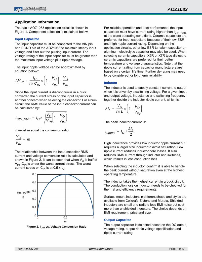
The relationship between the input capacitor RMS current and voltage conversion ratio is calculated and shown in Figure 2. It can be seen that when VO is half of VIN, CIN is under the worst current stress. The worst current stress on CIN is at 0.5 x IO.
Figure 2. ICIN vs. Voltage Conversion Ratio
For reliable operation and best performance, the input capacitors must have current rating higher than ICIN_RMS at the worst operating conditions. Ceramic capacitors are preferred for input capacitors because of their low ESR and high ripple current rating. Depending on the application circuits, other low ESR tantalum capacitor or aluminum electrolytic capacitor may also be used. When selecting ceramic capacitors, X5R or X7R type dielectric ceramic capacitors are preferred for their better temperature and voltage characteristics. Note that the ripple current rating from capacitor manufacturers are based on a certain life time. Further de-rating may need to be considered for long term reliability.
InductorThe inductor is used to supply constant current to output when it is driven by a switching voltage. For a given input and output voltage, inductance and switching frequency together decide the inductor ripple current, which is:
The peak inductor current is:
High inductance provides low inductor ripple current but requires a larger size inductor to avoid saturation. Low ripple current reduces inductor core losses. It also reduces RMS current through inductor and switches, which results in less conduction loss.
When selecting the inductor, confirm it is able to handle the peak current without saturation even at the highest operating temperature.
The inductor takes the highest current in a buck circuit. The conduction loss on inductor needs to be checked for thermal and efficiency requirements.
Surface mount inductors in different shape and styles are available from Coilcraft, Elytone and Murata. Shielded inductors are small and radiate less EMI noise but cost more than unshielded inductors. The choice depends on EMI requirement, price and size.
Output CapacitorThe output capacitor is selected based on the DC output voltage rating, output ripple voltage specification and ripple current rating.
ΔVINIO
f CIN×----------------- 1
VO
VIN---------–
⎝ ⎠⎜ ⎟⎛ ⎞ VO
VIN---------××=
ICIN_RMS IOVOVIN--------- 1
VOVIN---------–
⎝ ⎠⎜ ⎟⎛ ⎞
×=
VOVIN--------- m=
0
0.1
0.2
0.3
0.4
0.5
0 0.5 1m
ICIN_RMS(m)
IO
ΔILVOf L×----------- 1 VO
VIN---------–
⎝ ⎠⎜ ⎟⎛ ⎞
×=
ILpeak IOΔIL2--------+=
AOZ1083
Rev. 1.0 July 2011 www.aosmd.com Page 8 of 12
The selected output capacitor must have a higher rated voltage specification than the maximum desired output voltage including ripple. De-rating needs to be considered for long term reliability.
Output ripple voltage specification is another important factor for selecting the output capacitor. In a buck converter circuit, output ripple voltage is determined by inductor value, switching frequency, output capacitor value and ESR. It can be calculated by the equation below:
where,
CO is output capacitor value, and
ESRCO is the equivalent series resistance of the output capacitor.
When a low ESR ceramic capacitor is used as the output capacitor, the impedance of the capacitor at the switching frequency dominates. Output ripple is mainly caused by capacitor value and inductor ripple current. The output ripple voltage calculation can be simplified to:
If the impedance of ESR at switching frequency dominates, the output ripple voltage is mainly decided by the capacitor ESR and inductor ripple current. The output ripple voltage calculation can be further simplified to:
For lower output ripple voltage across the entire operating temperature range, X5R or X7R dielectric type of ceramic, or other low ESR tantalum capacitors or aluminum electrolytic capacitors may also be used as output capacitors.
In a buck converter, output capacitor current is continuous. The RMS current of output capacitor is decided by the peak to peak inductor ripple current. It can be calculated by:
Usually, the ripple current rating of the output capacitor is a smaller issue because of the low current stress. When the buck inductor is selected to be very small and inductor ripple current is high, the output capacitor could be overstressed.
Schottky Diode SelectionThe external freewheeling diode supplies the current to the inductor when the high side NMOS switch is off. To reduce the losses due to the forward voltage drop and recovery of diode, Schottky diode is recommended to use. The maximum reverse voltage rating of the chosen Schottky diode should be greater than the maximum input voltage, and the current rating should be greater than the maximum load current.
Thermal Management and Layout ConsiderationsIn the AOZ1083 buck regulator circuit, high pulsing current flows through two circuit loops. The first loop starts from the input capacitors, to the VIN pin, to the LX pin, to the filter inductor, to the output capacitor and load, and then returns to the input capacitor through ground. Current flows in the first loop when the high side switch is on. The second loop starts from the inductor, to the output capacitor and load, to the anode of Schottky diode, to the cathode of Schottky diode. Current flows in the second loop when the low side diode is on.
In PCB layout, minimizing the area of the two loops reduces the noise of the circuit and improves efficiency. A ground plane is strongly recommended to connect input capacitor, output capacitor, and PGND pin of the AOZ1083.
In the AOZ1083 buck regulator circuit, the major power dissipating components are the AOZ1083, the Schottky diode and output inductor. The total power dissipation of the converter circuit can be measured by input power minus output power:
The power dissipation in the Schottky diode can be approximated as:
where,
VFW_Schottky is the Schottky diode forward voltage drop.
The power dissipation of the inductor can be approximately calculated by output current and DCR of the inductor.
ΔVO ΔIL ESRCO1
8 f CO××-------------------------+⎝ ⎠
⎛ ⎞×=
ΔVO ΔIL1
8 f CO××-------------------------×=
ΔVO ΔIL ESRCO×=
ICO_RMSΔIL12----------=
Ptotal_loss VIN IIN×( ) VO VIN×( )–=
Pdiode_loss IO 1 D–( ) VFW_Schottky××=
Pinductor_loss IO2 Rinductor 1.1××=
AOZ1083
Rev. 1.0 July 2011 www.aosmd.com Page 9 of 12
The actual junction temperature can be calculated with power dissipation in the AOZ1281 and thermal impedance from junction to ambient.
The maximum junction temperature of AOZ1083 is 150 ºC, which limits the maximum load current capability.
The thermal performance of the AOZ1083 is strongly affected by the PCB layout. Care should be taken during the design process to ensure that the IC will operate under the recommended environmental conditions.
Several layout tips are listed below for the best electric and thermal performance.
1. The input capacitor should be connected as close as possible to the VIN pin and the GND pin.
2. The inductor should be placed as close as possible to the LX pin and the output capacitor.
3. Keep the connection of schottky diode between the LX pin and the GND pin as short and wide as possible.
4. Place the feedback resistors and compensation components as close to the chip as possible.
5. Keep sensitive signal traces away from the LX pin.
6. Pour a maximized copper area to the VIN pin, the LX pin and especially the GND pin to help thermal dissipation.
7. Pour copper plane on all unused board areas and connect the plane to stable DC nodes, like VIN, GND or VOUT.
TjunctionPtotal_loss Pdiode_loss Pinductor_loss––( ) Θ× JA
Tamb+=
AOZ1083
Rev. 1.0 July 2011 www.aosmd.com Page 10 of 12
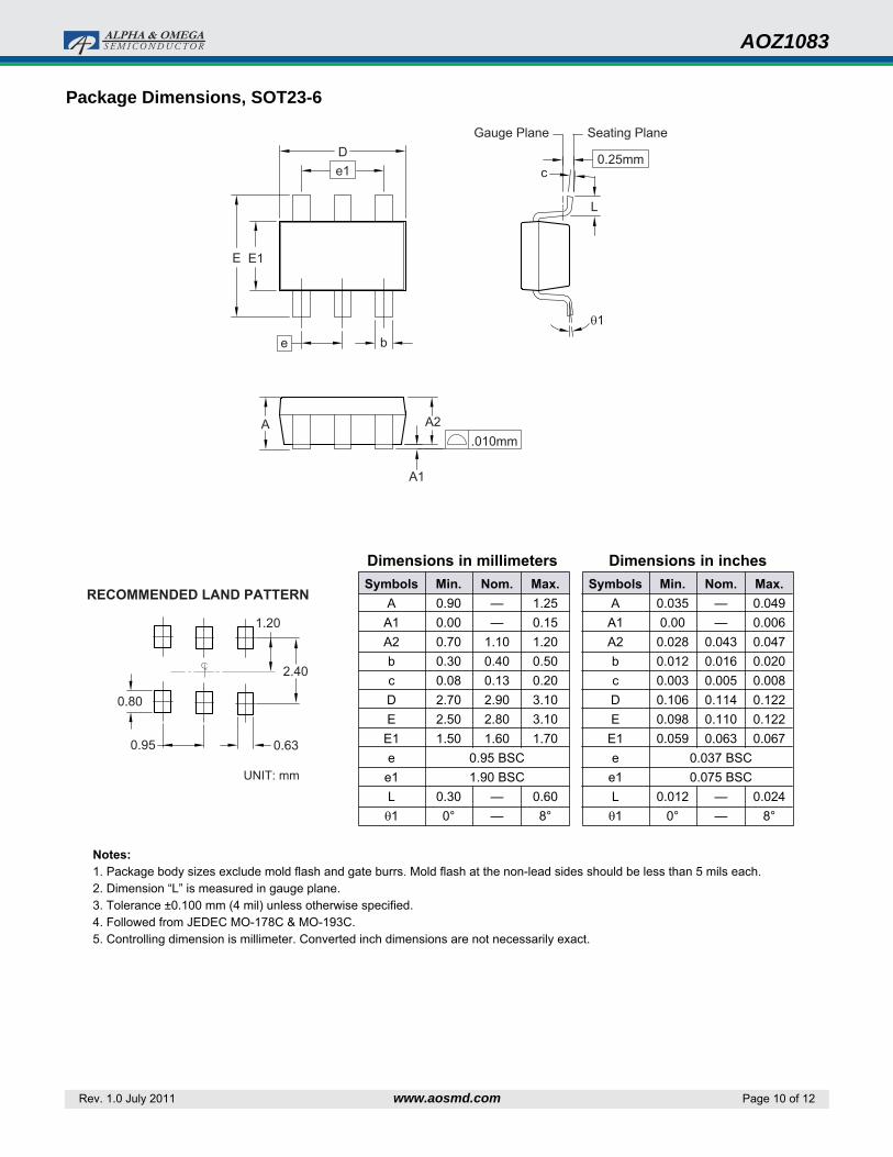
Package Dimensions, SOT23-6
E1E
A A2
A1
e
e1D
.010mm
0.80
0.95 0.63
2.40
b
L
c
Gauge Plane Seating Plane
0.25mm
θ1
1.20
Notes:
1. Package body sizes exclude mold flash and gate burrs. Mold flash at the non-lead sides should be less than 5 mils each.2. Dimension “L” is measured in gauge plane.3. Tolerance ±0.100 mm (4 mil) unless otherwise specified.4. Followed from JEDEC MO-178C & MO-193C.5. Controlling dimension is millimeter. Converted inch dimensions are not necessarily exact.
Symbols
AA1A2bcDE
E1e
e1Lθ1
Dimensions in millimeters
Min.
0.900.000.700.300.082.702.501.50
0.300°
Nom.
——
1.100.400.132.902.801.60
0.95 BSC1.90 BSC
——
Max.
1.250.151.200.500.203.103.101.70
0.608°
Symbols
AA1A2bcDE
E1e
e1Lθ1
Min.
0.0350.00
0.0280.0120.0030.1060.0980.059
0.0120°
Nom.
——
0.0430.0160.0050.1140.1100.063
0.037 BSC0.075 BSC
——
Max.
0.0490.0060.0470.0200.0080.1220.1220.067
0.0248°
Dimensions in inches
UNIT: mm
RECOMMENDED LAND PATTERN
AOZ1083
Rev. 1.0 July 2011 www.aosmd.com Page 11 of 12
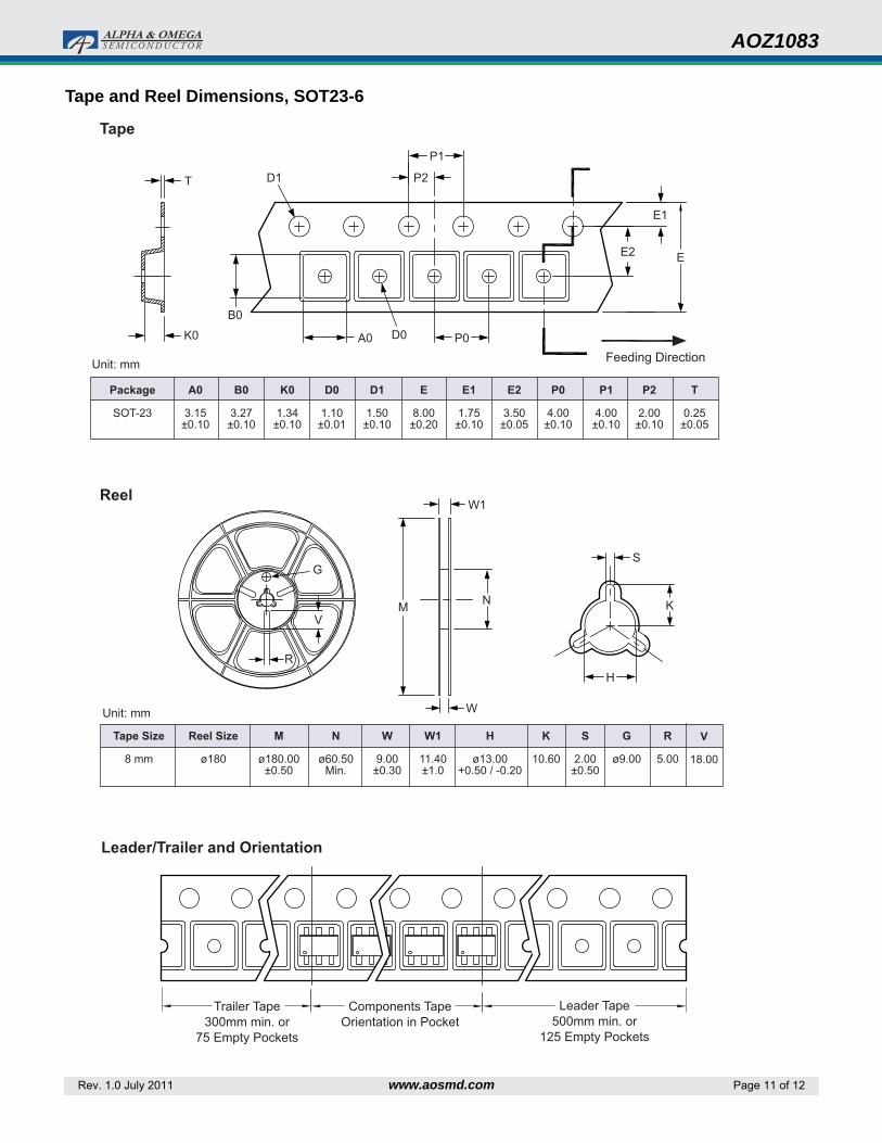
Tape and Reel Dimensions, SOT23-6
Tape
Reel
Leader/Trailer and Orientation
Trailer Tape300mm min. or
75 Empty Pockets
Components TapeOrientation in Pocket
Leader Tape500mm min. or
125 Empty Pockets
Unit: mm
Unit: mm
G
V
Feeding Direction
Tape Size
8 mm
Reel Size
ø180
M
ø180.00±0.50
N
ø60.50Min.
W1
11.40±1.0
W
9.00±0.30
Package
SOT-23
A0
3.15±0.10
B0
3.27±0.10
K0
1.34±0.10
D0
1.10±0.01
D1
1.50±0.10
E
8.00±0.20
E1
1.75±0.10
E2
3.50±0.05
P0
4.00±0.10
P1
4.00±0.10
P2
2.00±0.10
T
0.25±0.05
H
ø13.00+0.50 / -0.20
K
10.60
S
2.00±0.50
G
ø9.00
R
5.00
T
K0
B0
D1
A0 D0
P2
P1
P0
E1
E2 E
V
18.00
R
W1
N
W
M
S
K
H
AOZ1083
Rev. 1.0 July 2011 www.aosmd.com Page 12 of 12
Part MarkingAOZ1083CI
(SOT23-6)
2DBA 11
Week & Year CodePart Number Code
Assembly Location Code
Assembly Lot Code
As used herein:
1. Life support devices or systems are devices or systems which, (a) are intended for surgical implant into the body or (b) support or sustain life, and (c) whose failure to perform when properly used in accordance with instructions for use provided in the labeling, can be reasonably expected to result in a significant injury of the user.
2. A critical component in any component of a life support, device, or system whose failure to perform can be reasonably expected to cause the failure of the life support device or system, or to affect its safety or effectiveness.
This data sheet contains preliminary data; supplementary data may be published at a later date. Alpha & Omega Semiconductor reserves the right to make changes at any time without notice.
LIFE SUPPORT POLICY
ALPHA & OMEGA SEMICONDUCTOR PRODUCTS ARE NOT AUTHORIZED FOR USE AS CRITICAL COMPONENTS IN LIFE SUPPORT DEVICES OR SYSTEMS.