1854 IEEE JOURNAL OF SOLID-STATE CIRCUITS, VOL. 47, NO. 8, AUGUST 2012
A 40-mW 7-bit 2.2-GS/s Time-InterleavedSubranging CMOS ADC for Low-Power Gigabit
Wireless CommunicationsI-Ning Ku, Zhiwei Xu, Yen-Cheng Kuan, Yen-Hsiang Wang, and Mau-Chung Frank Chang
Abstract—A 7-bit, 2.2-GS/s time-interleaved subranging CMOSanalog-to-digital converter (ADC) for low-power gigabit wirelesscommunication system-on-a-chip (SoC) is presented. A time-split-ting subranging architecture is invented to significantly boost thespeed of individual ADC channels. In addition, a low-power andfast-settling distributed resistor array for reference voltages is pro-posed to mitigate gain mismatches within channels. Moreover, thechannel offset mismatches are calibrated through the digital- con-trolled corrective current sources embedded in the track-and-holdamplifiers of each sub-ADC. The prototype is implemented in 65nm CMOS, occupying only 0.3 mm chip area and consuming 40mW at 2.2 GS/s from a 1 V supply. Measured signal-to-noise anddistortion ratio (SNDR) and spurious-free dynamic range (SFDR)are 38 dB and 46 dB, respectively, with a 1.08 GHz input at 2.2 GS/ssampling rate. The effective number of bits (ENOB) is 6.0 bits atNyquist rate, and the figure-of-merit (F.O.M.) is 0.28 pJ/conv.-step.This prototype has also been integrated into a gigabit self-healingwireless transceiver SoC.
Index Terms—Analog-to-digital conversion, CMOS analog inte-grated circuits, subranging A/D converters, switched capacitor cir-cuits, time-interleaved ADC (TI-ADC).
I. INTRODUCTION
T HE ubiquitous access and usage of digital informationcontent has inevitably increased the communication data
rate requirement for a variety of applications. Also, wirelesshas become the most popular communication medium due toits user-friendly and hassle-free operation with mobility sup-port. To support the demands of high data rate wireless applica-tions, the 7 GHz unlicensed millimeter wave (mm-Wave) bandspanning from 57–64 GHz has been allocated by the FCC. It re-sults in several standard developments, such as IEEE 802.15.3c,IEEE 802.11ad, WirelessHD, etc., dedicated to multi-gigabitwireless communication systems. One of their common and ul-timate goals is to expedite the realization of widespread inte-grated circuits supporting large wireless data transfers.To achieve gigabit wireless communication in the 7 GHz
unlicensed 60 GHz band, a low order data modulation,
Manuscript received November 28, 2011; revised February 06, 2012; ac-cepted March 21, 2012. Date of publication June 05, 2012; date of current ver-sion July 19, 2012. This paper was approved by Guest Editor Hasnain Lak-dawala.The authors are with the Department of Electrical Engineering, Univer-
at http://ieeexplore.ieee.org.Digital Object Identifier 10.1109/JSSC.2012.2196731
such as BPSK or QPSK, is often adopted due to the wideapplicable bandwidth and modest circuit implementation com-plexity. Therefore, medium-resolution (6–8 bits), high-speed( ) CMOS ADCs are particularly critical to providepower-efficient, low-cost SoC solutions for such applications[1]–[6]. Though a single ADC running beyond GHz is feasiblein the advanced CMOS nodes, a time-interleaved ADC ispreferable due to its capability to achieve better power effi-ciency by combining multiple sub-ADCs operating at a lowersampling rate to deliver the required high sampling rate. Thetime-interleaved architecture, however, suffers from channelmismatches in timing, offset, and gain among individualsub-ADCs. Also, as the number of channels increases, the totalarea increases proportionally, which significantly complicatesthe associated routing of multiple phase clock signals and dig-ital outputs. The long routing wires of the clocks and outputsunavoidably introduce excessive parasitic capacitance, whichresults in a significant power penalty compared to individualsub-ADC. To achieve high power efficiency and performance,a proper choice of sub-ADC architecture and an effectivestrategy of alleviating channel mismatches are crucial to thetime-interleaved ADC design.Recent publications have adopted successive-approximation-
register ADCs (SAR-ADCs) [3], [7] and pipelined ADCs [4]as the sub-ADCs in a time-interleaved architecture. Despite itspower efficiency, the sampling rate of the SAR ADC is stilllimited since a large number of comparisons, at least one foreach bit, needs to happen in each sampling period. Therefore,a time-interleaved SAR ADC requires a large number of chan-nels, which in turn increases the overall chip area and powerconsumption. On the other hand, pipelined ADCs can operateat higher speeds; however, it imposes a stringent gain-band-width requirement on the op-amps, which becomes more andmore difficult to realize as scaled CMOS supply voltages con-tinue to decrease. With regard to the methodologies to miti-gate notorious channel mismatches of time-interleaved ADCs,research has been conducted to mitigate these through digitalsignal processing (DSP) approaches [8]–[12]. However, theirintensive usage of digital function blocks, such as adaptive filterand FFT processor, may lead to significant chip area or powerconsumption overhead after implementation, making those DSPapproaches unfavorable for a modest resolution, high speed,while low power and compact ADC.In this work, a 7-bit, 2.2-GS/s CMOSADC utilizing a number
of analog-centric and light-weight digital design techniques to
KU et al.: A 40-mW 7-bit 2.2-GS/s TIME-INTERLEAVED SUBRANGING CMOS ADC FOR LOW-POWER GIGABIT WIRELESS COMMUNICATIONS 1855
Fig. 1. Time-interleaved ADC architecture.
overcome the limitations of the time-interleaved architectureis described [13]. A time-splitting subranging ADC architec-ture that can offer significant higher sampling rate is invented,and is used as the sub-ADC in the interleaved ADC. This com-pact sub-ADC greatly reduces the required number of chan-nels and thus the total chip area. To achieve high power effi-ciency, a distributed resistor array is further proposed to gen-erate reference voltages for the time-interleaved ADC. It alle-viates channel gain mismatches by exploiting better matchingcharacteristics of poly resistors in the applied technology, whilesimultaneously maintains minimum power consumption over-head and fast settling response. Moreover, digitally controlledcurrent sources embedded in each sub-ADC correct for dc offsetmismatch between channels.This paper is organized as follows. Section II introduces
the architecture of the time-interleaved ADC, and Section IIIillustrates the proposed subranging ADC architecture. Twochannel mismatch reduction techniques, distributed resistorarray reference and digital offset calibration are presented inSection IV. Section V describes the circuit implementation ofcritical building blocks. Section VI presents the experimentalresults, and Section VII concludes the paper.
II. TIME-INTERLEAVED ADC ARCHITECTURE
Fig. 1 shows the proposed time-interleaved ADC block di-agram. A dedicated front-end track-and-hold amplifier (THA)samples the input signal at a full clock rate of 2.2 GHz. Itremoves the timing mismatches induced by unequal input delayand clock skew among interleaved channels. To achieve a com-pact and low-power realization in 65 nm CMOS, the numberof ADC channels must be minimized. After eliminating SARand pipelined architectures due to their low sampling rates andstrict op-amp design requirements as mentioned above, thesubranging and flash architectures are the remaining candidatesto build the sub-ADCs. Subranging ADCs have a much smallerarea and less power consumption than their flash counterpartsthough their conversion rate is lower. To compensate for thisspeed difference, a time-splitting high-speed 7-bit sub-ADC
with sample rate is invented, and adopted as thesub-ADC architecture. It reduces the required number of inter-leaved ADC channels down to four, and greatly simplifies themismatch calibration and routing complexity. After sub-ADCquantization, the digital outputs from individual sub-ADCsare then multiplexed to constitute a full rate 2.2 GS/s digitaloutput. The 550 MHz multiphase clocks for each sub-ADCare generated by a divide-by-four circuit, where the four-phaseclock outputs are delayed by a 90 phase shift from eachother. An on-chip reference generator distributes the referencevoltages to the sub-ADCs, and provides current biases for eachcircuit block.
III. TIME-SPLITTING SUBRANGING ADC
Through two-step conversion, the subranging architectureavoids the exponential growth in power and area of the flasharchitecture, while maintaining fairly high speed operation. Theconventional subranging architecture, however, hardly meetsthe design specification of 550 MS/s due to a tight timingbudget. In order to boost the subranging ADC operating speed,the tight timing budget, which mandates a complete signalquantization within a clock period, must be broken. We, herein,proposed a time-splitting architecture to relax the timing budgetby accomplishing the conversion of the subranging ADC intwo clock phases instead of one through pipeline processing.Fig. 2 shows the architecture of the 7-bit subranging ADC.It consists of a sub-THA, a 4-bit coarse ADC (CADC) and a4-bit fine ADC (FADC). The quantization procedure occursin two phases. In phase 1, the sub-THA tracks the inputsignal and CADC is in reset mode, where it samples thereference voltage. In phase 2, the sub-THA output is connectedto the CADC, where it is in amplification mode, while FADCsamples the sub-THA held output voltage . Then in thefollowing phase (phase 1), the references is connected to theFADC, where it amplifies the difference between and thecorresponding reference voltage based on CADC digital output
. As revealed by the timing diagram in Fig. 3(a),CADC must perform amplification, comparison and digital
1856 IEEE JOURNAL OF SOLID-STATE CIRCUITS, VOL. 47, NO. 8, AUGUST 2012
encoding within half a clock cycle. The time allowed foramplification is expressed as
(1)
where is the sampling period, is the comparatorregeneration time and & are the digital encoding
time of the CADC and FADC, respectively. In the employed65 nm CMOS technology, the typical comparator regenerationtime and digital encoding time are around . Thesebecome worse over process corner and temperature variation,granting insufficient time for the CADC amplification, therebylimiting the sampling rate of a conventional subranging ADC.Either an extra sample-and-hold (S/H) for time-interleaving is
KU et al.: A 40-mW 7-bit 2.2-GS/s TIME-INTERLEAVED SUBRANGING CMOS ADC FOR LOW-POWER GIGABIT WIRELESS COMMUNICATIONS 1857
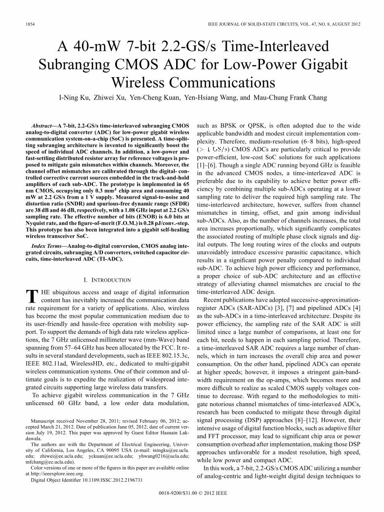
Fig. 4. Load reduction in sub-THA for conventional and proposed architecture.
required [14], which increases the total chip area, or extensiveamount of power is consumed to boost up the subrangingADC speed [15].To overcome this limitation and break the tight timing
budget, a time-splitting subranging architecture is proposed.Its timing diagram is illustrated in Fig. 3(b). The track/holdtime of the sub-THA is now shifted by ¼ clock cycle. More-over, phase 1 and phase 2 are exchanged in the CADC. Thisphase-exchanging scheme leads to different sampling instancesof CADC and FADC. In phase 1, the sub-THA tracks andamplifies the analog input signal, while CADC amplifies thesub-THA output concurrently. In phase 2, CADC initializesthe comparison and encodes the digital output for theFADC, and then amplifies the signal in the subsequent phase.The proposed architecture has two main advantages: First,the CADC amplification and encoding time are now split intotwo phases instead of one. As shown in the timing diagram,the CADC amplification time is shifted to the left occupyingthe entire phase 1, where phase 2 is dedicated for CADCdigital encoding. With a much more relaxed timing budget,the amplifier and comparator plus digital encoders now canoperate separately within half a clock cycle. This empowersthe subranging ADC to achieve a much higher conversion ratewith lower power consumption. The second advantage is thatthis architecture distributes the loading to sub-THA in differentphases by CADC and FADC. This is illustrated in Fig. 4. In the
conventional subranging architecture, the sub-THA output ca-pacitance loading is its intrinsic loading in phase 1 and thecombined input capacitance of CADC and FADC in phase 2. Inthe proposed architecture, the CADC and FADC capacitancesare distributed to different phases, where it evens the loadingimposed to the sub-THA in each phase. Since the requiredbandwidth for the sub-THA is proportional to the maximumloading across both phases, an evenly distributed loading canreduce the sub-THA bandwidth requirement leading to powersaving, and result in further power reduction in the sub-THAbuffer. The similar circumstance applies to the referencevoltage buffer as well. The capacitive loading imposed to thereference voltage buffer is also distributed across both phases,thereby reducing its power consumption.One issue associated with this architecture is the sub-THA in-
complete settling in phase 1. As shown in Fig. 3(b), the sampledvoltage across the CADC input capacitor may not settle within7 bits accuracy at the end of phase 1 since only ¼ clock period isallocated for the sub-THA during CADC amplification. This in-complete settling, however, can be mitigated by using the digitalerror correction circuit. Similar to the early comparison schemein pipelined ADC [17], as long as the error voltage is less than4 LSBs (16 mV), it can be corrected with one bit redundancy inthe CADC. Another drawback of this architecture is the reducedsub-THA tracking time. This can be compensated with a largerswitch and a larger clock driver that slightly increase the dig-
1858 IEEE JOURNAL OF SOLID-STATE CIRCUITS, VOL. 47, NO. 8, AUGUST 2012
ital power, which only constitutes a small portion of the overallpower consumption. Simulation shows that the single-channel7-bit subranging ADC running at 550 MS/s only consumes 7mW,which is much smaller compared to subranging ADCswithsimilar specifications [15], [16] and validates the proposed ar-chitecture.
IV. LOW-POWER CHANNEL MISMATCH REDUCTIONTECHNIQUES
To alleviate the effect of channel mismatch in time-inter-leaved ADCs, circuit techniques to improve matching betweenchannels are required. Moreover, correction circuitries withminimum power and area overhead are essential, especially forhigh-speed, medium resolution ADCs. A pure digital solutionis enticing due to its isolation from analog blocks that normallyneed to deliver speed and resolution. However, it may not bethe most efficient because it does not correct the errors existingin each analog block. An alternative approach is to calibratethe error by using analog correction with fine digital controls,where the corrections are executed offline at a low speed. Inthis section, two low-power mismatch reduction techniques,distributed resistor array reference and digital offset calibra-tion, are proposed to mitigate the non-idealities caused by gainmismatch and offset mismatch.
A. Distributed Resistor Array References
For sub-ADCs implemented in a flash-type architecture, themajor source of gain mismatch is reference voltage mismatch.As shown in Fig. 5(a), a conventional time-interleaved ADCuses high-speed buffers to distribute reference voltages to eachchannel. This approach, however, has two serious drawbacks:first, the small buffer transistor, to ensure high-speed operation,generates reference voltage mismatches among interleavedchannels, and therefore leads to large channel gain mismatch.Second, the high-speed buffer tends to consume large power,and a large number of high speed buffers further exacerbatesthe power consumption. To realize a low-power reference gen-erator with small channel gain mismatch, a distributed resistorarray as reference voltage generator is proposed, as shownin Fig. 5(b). Two low-speed buffers provide global voltages,
and , to the four parallel resistor arrays in thesub-ADCs, where the reference voltages are generatedwithin each resistor arrays. With resistors in each array, anda mismatch of for each resistor, the reference voltage
where is the ideal reference voltage without resistor mis-match. The reference voltage mismatch then can be expressedas
(3)
Given and poly resistor matchingin the applied 65 nm CMOS, the reference voltage mismatchachieves an accuracy of 0.07%. Since the resistor array can berealized with small resistor value by increasing area and intro-ducing minor speed penalty, a fast settling less than 1 ns canbe expected. The two buffers only need to provide DC currentto the resistor arrays instead of taking part in the high speedsettling. With the same DC current, the proposed resistor arrayachieves a lower output impedance compared with that of theactive CMOS devices in 65 nm CMOS. Consequently, a largeamplifier gain-bandwidth is not necessary and the overall powerconsumption can be reduced noticeably. Two additional largecapacitors are applied at the buffer output to further stabilizethe reference voltages and reduce the kickback noise from thesub-ADCs. In summary, the proposed distributed resistor arraycan provide accurate multi-channel on-chip voltage referenceswith much lower power consumption than conventional activeCMOS buffer realization.
B. Channel Offset Calibration
Channel offset mismatch originates from the DC offset ofsub-ADCs and contributes to noise tones at frequencies and
[18], [19], where is the sampling frequency. The conven-tional way of reducing mismatch is to increase transistor size,hence averaging out the random process variation. However, in
KU et al.: A 40-mW 7-bit 2.2-GS/s TIME-INTERLEAVED SUBRANGING CMOS ADC FOR LOW-POWER GIGABIT WIRELESS COMMUNICATIONS 1859
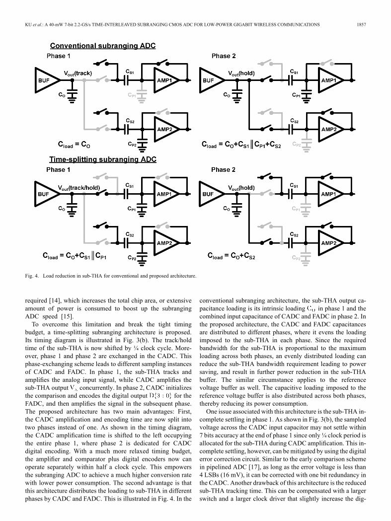
Fig. 6. Architecture of channel offset calibration circuit and its calibration procedure.
order to obtain an offset voltage less than 1/10 LSB, a large tran-sistor dimension is required. This not only inevitably increasesthe total chip area, but also results in large sub-ADC input ca-pacitance. To alleviate this tradeoff, transistors with minimumsize are employed and the corresponding DC offsets of eachchannel are calibrated out digitally during start-up. Fig. 6 showsthe architecture of the channel offset calibration circuit. For eachindividual channel, the input-referred offset is corrected by ad-justing additional binary-weighted current sources inside thesub-THA buffers [20]. During calibration, the clock rate is low-ered to 100 MHz due to the speed limitation of the synthesizedcalibration logic. The sub-ADC input terminals are connectedtogether, and the digital outputs are read out to determine theoffset voltage. Assume the source follower has unity gain, andlet and , the standard deviation ofthe offset voltage at the sub-ADC input can be expressed as
(4)
where is the charge injection mismatch of the samplingswitch & , is mismatch of input device& and is the mismatch of ADC itself. By
adjusting the corrective current , it is able to correct the
Fig. 7. Schematic of the main THA.
offset voltage, which is typically dominated by the thresholdvoltage mismatch of & . The calibration procedure isillustrated as follows (Fig. 6): In the first cycle, depending onthe output code , the corrective current will switch inthe direction of compensating the offset voltage. In the next fewcycles, the corrective current is then adjusted by switchingon/off the binary-weighted current sources in sequence tocalibrate the offset voltage, as indicated in (4). As shown inFig. 6, the digital output toggles between 63 and 64 at the endof calibration, and the offset voltage converges to a finite smallvalue in six clock cycles. The calibration is able to correct amaximum offset voltage of 10 mV and an accuracy of morethan 10 bits can be achieved. Since the calibration is executedoffline, it consumes negligible power when the ADC is innormal operation. It is worth noting that the introduction of thecalibration current cells in the sub-THA buffer only increasesthe power consumption negligibly to maintain an identicalbuffer gain-bandwidth due to their small capacitance load.
1860 IEEE JOURNAL OF SOLID-STATE CIRCUITS, VOL. 47, NO. 8, AUGUST 2012
Fig. 8. 4-bit CADC block diagram.
Fig. 9. 4-bit FADC block diagram.
V. CIRCUIT IMPLEMENTATION
A. Main Track-and-Hold Amplifier
In this work, a main THA operating at full clock rate of2.2 GS/s is designed to capture an input signal bandwidth1 GHz and remove the timing mismatch for the followinginterleaved channels. As illustrated in Fig. 7, the main THA isimplemented with an open-loop pseudo-differential architec-ture with bootstrapped switches used in [21]. An NMOS sourcefollower is employed to operate at a high speed of 2.2 GHz.The sampling capacitors for both the main THA and sub-THAare , which gives an input-referred noise of440 . While threshold voltage variation due to body-effectcan be avoided by tying the bulk of to the source, non-linearity caused by channel length modulation still remains.Nevertheless, this effect is tolerable for a 7-bit applicationand simulation demonstrates that the maximum harmonic is
in worst-case corner.
B. Coarse ADC
The 4-bit CADC block diagram is shown in Fig. 8. It consistsof 14 unit arrays of pre-amplifier and comparator, and a resistorarray that provides the coarse reference voltages. Since one re-dundant bit over-range is used for digital error correction, thenoise and offset requirements of the CADC are greatly relaxed.A maximum error up to 16 mV (4 LSB) can be tolerated. Con-sequently, the associated transistor and capacitor sizes can bemade small, resulting in more power and area saving.
C. Fine ADC
Since the FADC determines the overall linearity of the con-verter, it is required to obtain an accuracy of 7-bit resolution.Fig. 9 illustrates the block diagram of the 4-bit FADC. Two set ofbinary-weighted capacitor arrays determine the reference levelfor the FADC according to the CADC digital output .To minimize the comparator offset, four cascaded pre-ampli-fier arrays preceding the comparator array are implemented. To
KU et al.: A 40-mW 7-bit 2.2-GS/s TIME-INTERLEAVED SUBRANGING CMOS ADC FOR LOW-POWER GIGABIT WIRELESS COMMUNICATIONS 1861
Fig. 10. FADC pre-amplifiers.
Fig. 11. Schematic of the reference voltage buffers.
satisfy a low kT/C noise requirement, a unit capacitor with avalue of 15 fF is chosen, which gives a total capacitance of
differentially in each capacitor array. Thelarge capacitance not only results in large area penalty, but alsoadd excessive loading to the sub-THA. Therefore, two timesinterpolation is employed in each pre-amp stage so that onlytwo sets of large sampling capacitor arrays are required, insteadof fifteen sets of capacitor arrays. Capacitor interpolation [22]is used in this design for two reasons: First, it doesn’t requireextra dummies to overcome boundary effect [23] as in resistorinterpolation. Second, DC offset cancellation is adopted in eachstage pre-amps through switched-capacitor input/output offsetstorage [24]. Fig. 10 shows stage 1–4 pre-amps for the FADC.The first stage pre-amp uses output offset storage, where smallersampling switches are utilized to reduce charge injection. Stage2–4 pre-amps use input/output offset storage, which is morepower efficient and offers faster reset speed. In order to reduce
Fig. 12. Die micrograph.
power consumption, a dynamic comparator [17] followed by SRlatch is implemented in this design.
1862 IEEE JOURNAL OF SOLID-STATE CIRCUITS, VOL. 47, NO. 8, AUGUST 2012
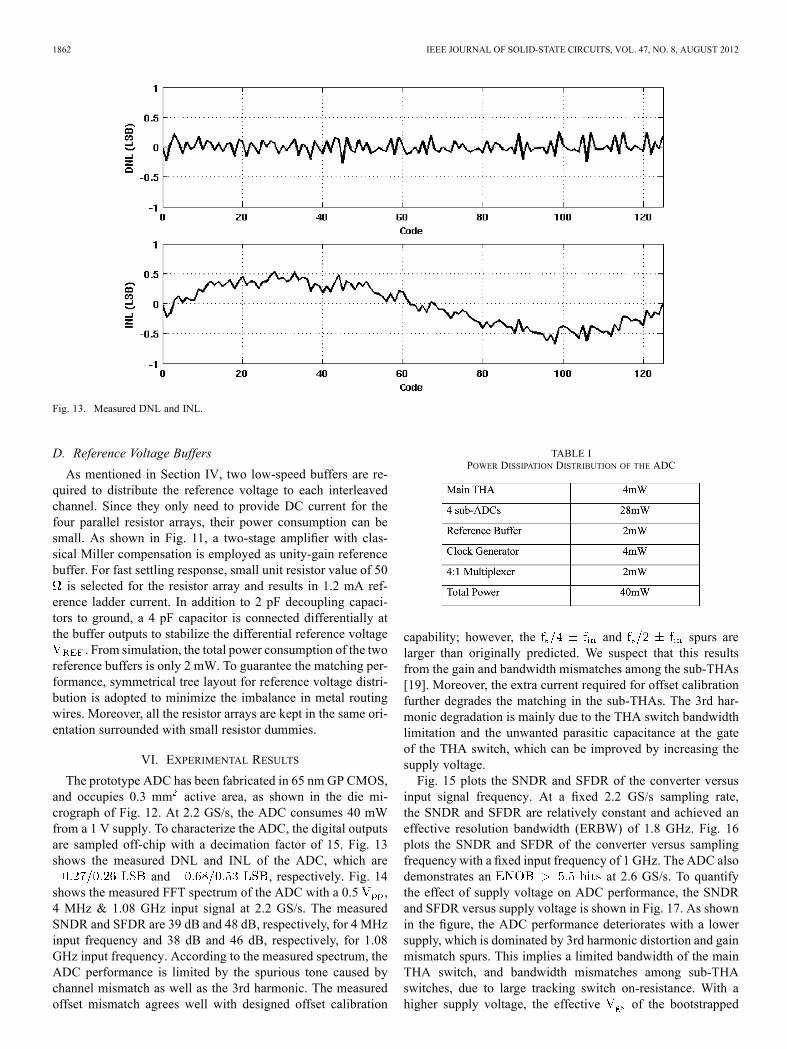
Fig. 13. Measured DNL and INL.
D. Reference Voltage Buffers
As mentioned in Section IV, two low-speed buffers are re-quired to distribute the reference voltage to each interleavedchannel. Since they only need to provide DC current for thefour parallel resistor arrays, their power consumption can besmall. As shown in Fig. 11, a two-stage amplifier with clas-sical Miller compensation is employed as unity-gain referencebuffer. For fast settling response, small unit resistor value of 50is selected for the resistor array and results in 1.2 mA ref-
erence ladder current. In addition to 2 pF decoupling capaci-tors to ground, a 4 pF capacitor is connected differentially atthe buffer outputs to stabilize the differential reference voltage
. From simulation, the total power consumption of the tworeference buffers is only 2 mW. To guarantee the matching per-formance, symmetrical tree layout for reference voltage distri-bution is adopted to minimize the imbalance in metal routingwires. Moreover, all the resistor arrays are kept in the same ori-entation surrounded with small resistor dummies.
VI. EXPERIMENTAL RESULTS
The prototype ADC has been fabricated in 65 nm GP CMOS,and occupies 0.3 mm active area, as shown in the die mi-crograph of Fig. 12. At 2.2 GS/s, the ADC consumes 40 mWfrom a 1 V supply. To characterize the ADC, the digital outputsare sampled off-chip with a decimation factor of 15. Fig. 13shows the measured DNL and INL of the ADC, which are
and , respectively. Fig. 14shows the measured FFT spectrum of the ADC with a 0.5 ,4 MHz & 1.08 GHz input signal at 2.2 GS/s. The measuredSNDR and SFDR are 39 dB and 48 dB, respectively, for 4 MHzinput frequency and 38 dB and 46 dB, respectively, for 1.08GHz input frequency. According to the measured spectrum, theADC performance is limited by the spurious tone caused bychannel mismatch as well as the 3rd harmonic. The measuredoffset mismatch agrees well with designed offset calibration
TABLE IPOWER DISSIPATION DISTRIBUTION OF THE ADC
capability; however, the and spurs arelarger than originally predicted. We suspect that this resultsfrom the gain and bandwidth mismatches among the sub-THAs[19]. Moreover, the extra current required for offset calibrationfurther degrades the matching in the sub-THAs. The 3rd har-monic degradation is mainly due to the THA switch bandwidthlimitation and the unwanted parasitic capacitance at the gateof the THA switch, which can be improved by increasing thesupply voltage.Fig. 15 plots the SNDR and SFDR of the converter versus
input signal frequency. At a fixed 2.2 GS/s sampling rate,the SNDR and SFDR are relatively constant and achieved aneffective resolution bandwidth (ERBW) of 1.8 GHz. Fig. 16plots the SNDR and SFDR of the converter versus samplingfrequency with a fixed input frequency of 1 GHz. The ADC alsodemonstrates an at 2.6 GS/s. To quantifythe effect of supply voltage on ADC performance, the SNDRand SFDR versus supply voltage is shown in Fig. 17. As shownin the figure, the ADC performance deteriorates with a lowersupply, which is dominated by 3rd harmonic distortion and gainmismatch spurs. This implies a limited bandwidth of the mainTHA switch, and bandwidth mismatches among sub-THAswitches, due to large tracking switch on-resistance. With ahigher supply voltage, the effective of the bootstrapped
KU et al.: A 40-mW 7-bit 2.2-GS/s TIME-INTERLEAVED SUBRANGING CMOS ADC FOR LOW-POWER GIGABIT WIRELESS COMMUNICATIONS 1863
TABLE IIPERFORMANCE SUMMARY AND COMPARISON
Fig. 14. Measured spectrum at 2.2 GS/s with (a) 4MHz and (b) 1.08 GHz inputfrequency.
switch increases, thus reducing the switch on-resistance. Theprototype ADC achieves a figure of merit (FOM) of 0.28pJ/conv.-step, which is defined as
(5)
Fig. 15. Measured SNDR and SFDR vs. input frequency at .
Fig. 16. Measured SNDR and SFDR vs. sampling frequency at .
Table I shows the power dissipation distribution for thisADC. The performance summary and its comparison tostate-of-the-art ADCs [3]–[6] with 7–8 bits resolution and
sampling rate is shown in Table II. To the authors’best knowledge, this ADC achieves the best F.O.M. and thesecond smallest active area in this category.
VII. CONCLUSION
A 7-bit, 2.2 GS/s time-interleaved subranging ADC forgigabit wireless communication systems has been described.
1864 IEEE JOURNAL OF SOLID-STATE CIRCUITS, VOL. 47, NO. 8, AUGUST 2012
Fig. 17. Measured SNDR and SFDR vs. supply voltage at .
The proposed time-splitting subranging architecture signifi-cantly increases the speed of individual ADC channels andreduces the total number of interleaved channels to onlyfour. By employing a distributed resistor array to produce thevoltage reference, channel gain mismatch is alleviated whilemaintaining low power consumption. Channel offset mismatchis calibrated through corrective current sources embedded inthe sub-THAs with small area overhead and negligible powerduring normal operation. The ADC is implemented in a 65 nmCMOS process, occupying 0.3 mm active area and consuming40 mW. The measured ENOB is 6.0 bits at Nyquist rate with aF.O.M. of 0.28 pJ/conv.-step. This ADC has also been success-fully integrated into a 60 GHz wireless transceiver for gigabitwireless applications.
ACKNOWLEDGMENT
Chip fabrication and technical support was generously pro-vided by TSMC Inc.
REFERENCES
[1] B. Verbruggen, J. Craninckx, M. Kuijk, P. Wambacq, and G. Vander Plas, “A 2.6 mW 6b 2.2 GS/s 4-times interleaved fully dynamicpipelined ADC in 40 nm digital CMOS,” in IEEE ISSCC Dig. Tech.Papers, Feb. 2010, pp. 296–297.
[2] Y. Nakajima et al., “A background self-calibrated 6 b 2.7 GS/s ADCwith cascade-calibrated folding-interpolating architecture,” IEEE J.Solid-State Circuits, vol. 45, no. 4, pp. 707–718, Apr. 2010.
[3] E. Alpman, H. Lakdawala, L. R. Carley, and K. Soumyanath, “A 1.1V 50 mW 2.5 GS/s 7 b time-interleaved C-2C SAR ADC in 45 nmLP digital CMOS,” in IEEE ISSCC Dig. Tech. Papers, Feb. 2009, pp.76–77.
[4] C. C. Hsu, C. C. Huang, Y. H. Lin, C. C. Lee, Z. Soe, T. Aytur, andR. H. Yan, “A 7 b 1.1 GS/s reconfigurable time-interleaved ADC in 90nm CMOS,” in Symp. VLSI Circuits Dig., Jun. 2007, pp. 66–67.
[5] T. Sundström, C. Svensson, and A. Alvandpour, “A 2.4 GS/s, 4.9ENOB at Nyquist, single-channel pipeline ADC in 65 nm CMOS,” inProc. ESSCIRC, Sep. 2010, pp. 370–373.
[6] J. Proesel, G. Keskin, J.-O. Plouchart, and L. Pileggi, “An 8-bit 1.5GS/s flash ADC using post-manufacturing statistical selection,” inProc. IEEE CICC, Sep. 2010.
[7] K. Doris, E. Janssen, C. Nani, A. Zanikopoulos, and G. van der Weide,“A 480 mW 2.6 GS/s 10 b time-interleaved ADC with 48.5 dB SNDRup to Nyquist in 65 nm CMOS,” IEEE J. Solid-State Circuits, vol. 46,no. 12, pp. 2821–2833, Dec. 2011.
[8] H. Jin and E. K. F. Lee, “A digital-background calibration techniquefor minimizing timing-error effects in time-interleaved ADCs,” IEEETrans. Circuits Syst. II, Analog Digit. Signal Process., vol. 47, no. 7,pp. 603–613, Jul. 2000.
[9] J. Elbornsson, F. Gustafsson, and J. Eklund, “Blind adaptive equaliza-tion of mismatch errors in a time-interleaved A/D converter system,”IEEE Trans. Circuits Syst. II, Exp. Briefs, vol. 51, no. 1, pp. 151–158,Jan. 2004.
[10] V. Divi and G. W. Wornell, “Blind calibration of timing skew in time-interleaved analog-to-digital converters,” IEEE J. Sel. Topics SignalProcess., vol. 3, no. 3, pp. 509–522, May 2009.
[11] S. Huang and B. C. Levy, “Blind calibration of timing offsets for fourchannel time-interleaved A/D converters,” IEEE Trans. Circuits Syst.I, Reg. Papers, vol. 54, no. 4, pp. 863–876, Apr. 2007.
[12] C. Law, P. J. Hurst, and S. H. Lewis, “A four-channel time-interleavedADC With digital calibration of interchannel timing and memory er-rors,” IEEE J. Solid-State Circuits, vol. 45, no. 10, pp. 2091–2103, Oct.2010.
[13] I. Ku, Z. Xu, Y. C. Kuan, Y. H. Wang, and M. F. Chang, “A 40-mW7-bit 2.2-GS/s time-interleaved subranging ADC for low-power gigabitwireless communications in 65-nm CMOS,” in Proc. IEEE CICC, Sep.2011.
[14] Z. Cao and S. Yan, “A 52 mW 10 b 210 MS/s two-step ADC for dig-ital-IF receivers in 0.13 m CMOS,” in Proc. IEEE CICC, Sep. 2008,pp. 309–312.
[15] K. Ohhata, K. Uchino, Y. Shimizu, K. Oyama, and K. Yamashita, “De-sign of a 770-MHz, 70-mW, 8-bit subranging ADC using referencevoltage precharging architecture,” IEEE J. Solid-State Circuits, vol. 44,no. 11, pp. 2881–2890, Nov. 2009.
[16] Y. Shimizu, S. Murayama, K. Kudoh, and H. Yatsuda, “A split-loadinterpolation-amplifier-array 300 MS/s 8 b subranging ADC in 90 nmCMOS,” in IEEE ISSCC Dig. Tech. Papers, Feb. 2008, pp. 552–635.
[17] B.-M.Min, P. Kim, F.W. Bowman, III, D.M. Boisvert, and A. J. Aude,“A 69-mW 10-bit 80- MSample/s pipelined CMOS ADC,” IEEE J.Solid-State Circuits, vol. 38, no. 12, pp. 2031–2039, Dec. 2003.
[18] W. C. Black and D. A. Hodges, “Time interleaved converter arrays,”IEEE J. Solid-State Circuits, vol. 15, no. 6, pp. 1022–1029, Dec. 1980.
[19] N. Kurosawa, H. Kobayashi, K. Maruyama, H. Sugawara, and K.Kobayashi, “Explicit analysis of channel mismatch effects in time-in-terleaved ADC systems,” IEEE Trans. Circuits Syst. I, vol. 48, no. 3,pp. 261–271, Mar. 2001.
[20] H. Yu andM.-C. F. Chang, “A 1-V 1.25-GS/S 8-bit self-calibrated flashADC in 90-nm digital CMOS,” IEEE Trans. Circuits Syst. II, vol. 55,no. 7, pp. 668–672, Jul. 2008.
[21] M. Dessouky and A. Kaiser, “Very low-voltage digital-audio mod-ulator with 88-dB dynamic range using local switch,” IEEE J. Solid-State Circuits, vol. 36, no. 3, pp. 349–355, Mar. 2001.
[22] K. Kusumoto, K. Murata, A. Matsuzawa, S. Tada, M. Maruyama, K.Oka, and H. Konishi, “A 10 b 20 MHz 30 mW pipelined interpo-lating CMOS ADC,” in IEEE ISSCC Dig. Tech. Papers, Feb. 1993,pp. 62–63.
[23] K. Bult and A. Buchwald, “An embedded 240-mW 10-b 50-MS/sCMOS ADC in 1-mm ,” IEEE J. Solid-State Circuits, vol. 32, no. 12,pp. 1887–1895, Dec. 1997.
[24] B. Razavi, Principles of Data Conversion System Design. New York:IEEE Press/Wiley-Interscience, 1995.
I-Ning Ku (S’07) received the B.S degree in elec-trophysics from National Chiao-Tung University(NCTU), Hsinchu, Taiwan, in 1999 and the M.S.and Ph.D. degrees in electrical engineering from theUniversity of California, Los Angeles, in 2001 and2011, respectively.He is currently with Broadcom Corporation,
Irvine, CA. Prior to joining Broadcom, he waswith SST Communications, Los Angeles, CA,from 2003–2008, and HRL Laboratories, Malibu,CA, in 2009. His research interests are high-speed
ADC/DAC design and precision mixed-signal IC design.
KU et al.: A 40-mW 7-bit 2.2-GS/s TIME-INTERLEAVED SUBRANGING CMOS ADC FOR LOW-POWER GIGABIT WIRELESS COMMUNICATIONS 1865
Zhiwei Xu (S’97–M’03–SM’10) received the B.S.and M.S. degree from Fudan University, Shanghai,China and Ph.D. from University of California, LoaAngeles, all in electrical engineering.He held industry positions with G-Plus Inc., SST
communications, Conexant Systems and NXP Inc.,where he led development for wireless LAN andSoC solutions for proprietary wireless multimediasystems, CMOS cellular transceiver, Multimediaover Cable (MoCA) system and TV tuners. He iscurrently with HRL laboratories, working on various
aspects of millimeter and sub-millimeter wave integrated circuit and system,software defined radios, high speed ADC and analog VLSI. He has publishedin various journals and conferences, one contribution to the encyclopedia ofwireless and mobile communications, about ten granted and pending patents.
Yen-Cheng Kuan received the B.S. degree in elec-trical engineering from National Taiwan University,Taipei, Taiwan, and the M.S. degree in electrical en-gineering from the University of California, Los An-geles, where he is currently pursuing the Ph.D. de-gree.From 2004 to 2007, he was a system engineer at
Realtek Semiconductor Corp., Irvine, CA, wherehe contributed to the design of Ultra-wideband(UWB) System-on-a-Chip. Since 2009, he has beenwith Hughes Research Laboratories (HRL), Malibu,
CA, working on software-defined radios, compressed-sensing receivers,and multi-rate signal processing for high-speed ADCs. His current researchinterests include transceiver algorithm and implementation for millimeter wave(60 GHz) communication systems, mixed-signal circuits, and communicationstandardizations.
Yen-Hsiang Wang (S’10) was born on February16th, 1986, in Taipei, Taiwan. He received theB.S. degree in electrical engineering from NationalTaiwan University (NTU), Taipei, Taiwan, in 2008,and the M.S. degree in electrical engineering fromUniversity of California, Los Angeles (UCLA),in 2011, where he is currently pursuing the Ph.D.degree.His research focuses on the design of high-perfor-
mance and low-power ADCs.
Mau-Chung Frank Chang (F’96) is the Wintek En-dowed Chair and Distinguished Professor of Elec-trical Engineering and the Chairman of the ElectricalEngineering Department, University of California atLos Angeles (UCLA).Before joining UCLA, he was the Assistant
Director and Department Manager of the HighSpeed Electronics Laboratory at Rockwell ScienceCenter (1983–1997), Thousand Oaks, California.In this tenure, he developed and transferred theAlGaAs/GaAs Heterojunction Bipolar Transistor
(HBT) and BiFET (Planar HBT/MESFET) integrated circuit technologiesfrom the research laboratory to the production line (now Conexant Systemsand Skyworks). The HBT/BiFET productions have grown into multi-billiondollar businesses and dominated the cell phone power amplifiers and front-endmodule markets (currently exceeding one billion units/year). Throughout hiscareer, his research has primarily focused on the development of high-speedsemiconductor devices and integrated circuits for RF and mixed-signal com-munication and imaging system applications. He was the principal investigatorat Rockwell in leading DARPA’s ultra-high speed ADC/DAC development fordirect conversion transceiver (DCT) and digital radar receivers (DRR) systems.He was the inventor of the multiband, reconfigurable RF-Interconnects, basedon FDMA and CDMA multiple access algorithms, for ChipMulti-Processor(CMP) inter-core communications and inter-chip CPU-to-Memory communi-cations. He also pioneered the development of world’s first multi-gigabit/secADC, DAC and DDS in both GaAs HBT and Si CMOS technologies; thefirst 60 GHz radio transceiver front-end based on transformer-folded-cascode(Origami) high-linearity circuit topology; and the low phase noise CMOSVCO ( ) with Digitally Controlled on-chip ArtificialDielectric (DiCAD). He was also the first to demonstrate CMOS oscillatorsin the Terahertz frequency spectrum (1.3 THz) and the first to demonstratea CMOS active imager at the sub-mm-Wave spectra (180 GHz) based on aTime-Encoded Digital Regenerative Receiver. He was also the founder of anRF design company G-Plus (now SST and Microchip) to commercialize WiFi11b/g/a/n power amplifiers, front-end modules and CMOS transceivers.He was elected to the US National Academy of Engineering in 2008 for the
development and commercialization of GaAs power amplifiers and integratedcircuits. He was also elected as a Fellow of IEEE in 1996 and received IEEEDavid Sarnoff Award in 2006 for developing and commercializing HBT poweramplifiers for modern wireless communication systems. He was the recipient of2008 PanWenYuan Foundation Award and 2009 CESASCCareer AchievementAward for his fundamental contributions in developing AlGaAs/GaAs hetero-junction bipolar transistors. His recent paper “A Blocker-Tolerant WidebandNoise Cancelling Receiver with 2 dB Noise Figure” was selected for the Distin-guished Technical Paper Award in 2012 IEEE International Solid State CircuitsConference (ISSCC). He received Rockwell’s Leonardo Da Vinci Award (En-gineer of the Year) in 1992; National Chiao Tung University’s DistinguishedAlumnus Award in 1997; and National Tsing Hua University’s DistinguishedEngineering Alumnus Award in 2002.