2284 IEEE JOURNAL OF SOLID-STATE CIRCUITS, VOL. 43, NO. 10, OCTOBER 2008
A 622-Mb/s Mixed-Mode BPSK Demodulator Usinga Half-Rate Bang-Bang Phase Detector
Duho Kim, Student Member, IEEE, Kwang-chun Choi, Young-kwang Seo, Hyunchin Kim, andWoo-Young Choi, Member, IEEE
Abstract—A new mixed-mode binary phase shift keying (BPSK)demodulator is demonstrated using a half-rate bang-bang phasedetector commonly used in clock and data recovery (CDR) appli-cations. This demodulator can be used for new home networkingapplications using already installed CATV lines. A prototype chiprealized by 0.18- m CMOS process can demodulate 622-Mb/s dataat 1.4-GHz carrier frequency. At this data rate, the demodulatorcore consumes 27.5 mW from a 1.8 V power supply while the corechip area is 210 150 m2. The transmission over 20-m CATVline using the prototype chip is successfully demonstrated.
Index Terms—Binary phase shift keying, CATV, Costas-loop, de-modulator, half-rate bang-bang phase detector, home networks,mixed-mode.
I. INTRODUCTION
T HERE are many A/V appliances at home such as DVDplayers, HDTV and satellite receivers. Establishing com-
munication among these appliances is an important marketdemand. However, installing new lines for linking home ap-pliances is not desirable and, consequently, approaches usingeither wireless channels or already-built-in wirelines are pre-ferred. For the second approach, using cable TV (CATV) linesthat are already installed in many houses can be an attractivesolution.
Fig. 1(a) schematically shows such an approach. A switchinghub and RF combiners are inside the wall with a CATV splitter.The switching hub connects a set-top box to many display ter-minals in several locations. In order to establish communicationchannels based on CATV lines, high-frequency carriers above 1GHz must be used so that CATV signals MHz are notdisturbed by data streams as can be seen in Fig. 1(b). Modemchips that satisfy this requirement are not easily available.
Although such modulation techniques as QPSK and QAM arepreferred since they utilize bandwidth more efficiently, we triedBPSK first because it is simpler and more suitable for the ini-tial trial. There are several types of BPSK demodulators. In theanalog approach, the carrier signal can be recovered by usinga phase-locked loop (PLL) after the received signal is squared
Manuscript received August 11, 2007; revised June 17, 2008. Current ver-sion published October 8, 2008. This work was supported by “System IC 2010”project of Korea Ministry of Knowledge Economy and the IC Design Educa-tion Center (IDEC), Korea, and by Digital Solution Center of CTO, SamsungElectronics Co. Ltd.
D. Kim, K. Choi, and W. Choi are with the Department of Electrical andElectronic Engineering, Yonsei University, Seoul 120-749, Korea (e-mail:[email protected]).
Y. Seo and H. Kim are with the Digital Solution Center of CTO, SamsungElectronics Co. Ltd., Gyeonggi-Do 443-742, Korea (e-mail: [email protected]).
Digital Object Identifier 10.1109/JSSC.2008.2004327
[1]. However, the phase error between the received and the re-covered signals remains. Using Costas-loop [2] is a classicalanalog approach but, as the frequency becomes higher, designcosts for filters and device matching increase. In the digital ap-proach, several different architectures are possible depending onADC configurations [3], but the maximum data rate is limitedby the speed of ADCs. The digital interpolation scheme [4], [5],which is the most popular digital approach, needs GSamples/sADCs to oversample hundreds of Mb/s data, but realization ofsuch ADCs is not easy. In this paper, we report a new CMOSmixed-mode BPSK demodulator for 1.4 GHz carrier frequencythat can handle 622 Mb/s for the above-mentioned application.
This paper is organized as follows. Section II analyzes estab-lished BPSK demodulation schemes. Section III introduces thenew mixed-mode demodulation scheme. Section IV describesthe implementation of the prototype chip. Section V gives mea-surement results of the fabricated chip.
II. ESTABLISHED DEMODULATION SCHEME
Fig. 2 is the block diagram of Costas-loop, the classic analogBPSK demodulator. Two sine waves with 90 phase differenceare multiplied to the modulated signal. Assuming is the phase
Authorized licensed use limited to: Yonsei University. Downloaded on October 8, 2008 at 23:11 from IEEE Xplore. Restrictions apply.
KIM et al.: A 622-Mb/s MIXED-MODE BPSK DEMODULATOR USING A HALF-RATE BANG-BANG PHASE DETECTOR 2285
Fig. 2. Block diagram of Costas-loop.
Fig. 3. Low-IF indirect conversion using digital interpolation.
difference between the modulated signal and the voltage-con-trolled oscillator (VCO), two output signals are given as
(1)
Low-pass filters (LPFs) remove high frequency terms having, so that only the terms having remain. The product of two
LPF outputs results in terms having square of , which isalways 1 since is either 1 or . Consequently the outputbecomes . The phase difference, , can be eliminated bya feedback-loop and is recovered.
For realization of Costas-loop for high frequency carrier ap-plications, it is difficult to implement LPFs. By using simple RCfilters, flatness of pass-band response and sharpness of cutoffband are poor. A large chip area is also needed due to capac-itors. Although better flatness and sharpness can be achievedwith other filter types, they usually require more chip areas. An-other problem arises from the mismatch of two signal paths inthe high frequency. This results in additional design costs.
In digital approach for BPSK demodulation, there are sev-eral variations depending on the ADC configuration, but ADCis usually located after the mixer. Fig. 3 shows an example of de-modulation flow using the digital interpolation technique. Afterthe mixer converts the RF signals to the IF domain, ADC sam-ples them with a sampling clock. Then, signals between sampleddata are produced by interpolation. The timing controller syn-chronizes interpolated signals in the digital domain and makesa decision. In this scheme, the minimum ADC sampling rate is
twice of the data rate to satisfy the Nyquist condition. To de-modulate higher order PSK signals, the ADC resolution has tobe higher.
Several CMOS ADCs operating at GSamples/s have been re-ported in [6]–[8]. But they usually require large power consump-tion and chip area. Consequently, the ADC performance limitsthe maximum data rate in the digital approach.
III. MIXED-MODE APPROACH
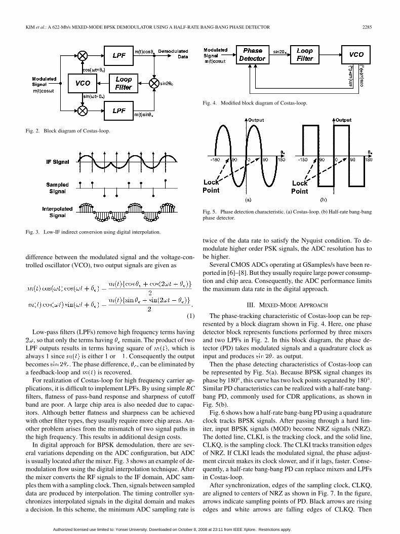
The phase-tracking characteristic of Costas-loop can be rep-resented by a block diagram shown in Fig. 4. Here, one phasedetector block represents functions performed by three mixersand two LPFs in Fig. 2. In this block diagram, the phase de-tector (PD) takes modulated signals and a quadrature clock asinput and produces as output.
Then the phase detecting characteristics of Costas-loop canbe represented by Fig. 5(a). Because BPSK signal changes itsphase by 180 , this curve has two lock points separated by 180 .Similar PD characteristics can be realized with a half-rate bang-bang PD, commonly used for CDR applications, as shown inFig. 5(b).
Fig. 6 shows how a half-rate bang-bang PD using a quadratureclock tracks BPSK signals. After passing through a hard lim-iter, input BPSK signals (MOD) become NRZ signals (NRZ).The dotted line, CLKI, is the tracking clock, and the solid line,CLKQ, is the sampling clock. The CLKI tracks transition edgesof NRZ. If CLKI leads the modulated signal, the phase adjust-ment circuit makes its clock slower, and if it lags, faster. Conse-quently, a half-rate bang-bang PD can replace mixers and LPFsin Costas-loop.
After synchronization, edges of the sampling clock, CLKQ,are aligned to centers of NRZ as shown in Fig. 7. In the figure,arrows indicate sampling points of PD. Black arrows are risingedges and white arrows are falling edges of CLKQ. Then
Authorized licensed use limited to: Yonsei University. Downloaded on October 8, 2008 at 23:11 from IEEE Xplore. Restrictions apply.
2286 IEEE JOURNAL OF SOLID-STATE CIRCUITS, VOL. 43, NO. 10, OCTOBER 2008
Fig. 6. BPSK signal tracking by half-rate bang-bang PD. (a) When clock leads.(b) Clock lags.
Fig. 7. Proposed demodulation scheme.
the bang-bang PD produces output sequence, SAM1, whichconsists of 10 and 01. The BPSK demodulation is done whendecisions are made for high for 10 sequence, and low for 01sequence. This can be easily realized by inverting samples atfalling edges of CLKQ, which makes 10 sequence 11, and01 sequence 00 (SAM2 in the figure). This BPSK demodu-lation scheme can use any type of CDR architectures using ahalf-rate PD.
When the carrier frequency is exactly the integer-multipleof the data rate, BPSK signal can be generated identically toNRZ signal. But it is impossible for a flexible data rate witha fixed carrier frequency. In the proposed scheme, data transi-tion is recognized when the receiver clock synchronized to thecarrier signals goes through the transition, not when the datago through the transition. When the carrier frequency is not ex-actly the integer-multiple of the data rate as shown in Fig. 8,data transitions occurring between receiver clock transitions arerecognized at the next clock transition, causing the quantizedtiming error, maximum of which is given as the half of carrierperiod. This affects jitter performance directly. Sampling clockis aligned to carrier phase, and therefore, it slips as shown infigure. After an half beating period, the difference of data rateand carrier frequency, the transition will return because adja-cent sampling clock is aligned again. Consequently, there occurslipping traces on eye diagram as shown. With a higher car-rier frequency, this quantized timing error is reduced. Since the
amount of jitter given in unit interval (UI) is proportional to theproduct of this quantization error and the data rate, the key pa-rameter for jitter performance in our demodulator is (Carrier fre-quency)/(Data rate).
It is easy to extend the proposed scheme into demodulationsof higher order PSKs. M-ary PSK modulation uses phasesto express symbols. For example, BPSK uses 0 and 180phases for 0 and 1 symbols, and QPSK uses 0 , 90 , 180 , and270 for 00, 01, 11, and 10. Demodulator for M-ary PSK modu-lated signal should have PD which has M lock points to maintainlocked state for input phases. Consequently, a 1/M-rate CDR cir-cuit can synchronize its clocks to M-ary PSK signal. With theproposed scheme, CDR circuit locks its frequency to the carrierfrequency not the data rate. Thus, 1/M rate CDR for data rate DRis capable of demodulating M-ary PSK signals with carrier fre-quency, DR/M. For example, 10-Gb/s half-rate CDR fabricatedwith 0.18 m CMOS process reported in [12] can be appliedto demodulate BPSK modulated signal with 5-GHz carrier. Asthe prototype BPSK demodulator chip shows maximum symbolrate of about half the carrier frequency, the maximum data ratewill be above 2 Gb/s.
IV. IMPLEMENTATION
A. Phase Control Scheme
Among the several kinds of phase control schemes for CDRapplications, the scheme of controlling VCO with PD outputis the most basic one. For this, the loop bandwidth influencesphase noises from input and power supply noises. The phasenoise characteristics are very important for demodulator appli-cations because phase noises can cause phase unlocking prob-lems, resulting in data errors. For the optimal performance, theprototype chip employs the semi-digital dual-loop delay-lockedloop (DLL) scheme [9], which separates loop bandwidth of PLLfrom input noises by using separate loops for clock genera-tion and phase tracking. This phase control scheme is alwaysstable because it is essentially DLL, type-I system. The fre-quency locking range of this scheme is limited by the operatingfrequency range of PLL. Fig. 9 shows a block diagram for theprototype chip. Since a half-rate bang-bang PD needs a quadra-ture clock, Phase-Interpolator2 and 4:2 MUX2 are added [10].These additional blocks are also controlled by the same phasecontroller and use 90 delayed input clocks.
The phase controller shifts the phase by the minimum step toalign tracking clock to input signal. The prototype chip has 6-bitresolution since it uses 4-bit phase interpolators and 4:2 MUXswith 2-bit select signal. The phase controller was implementedby auto placement and routing of standard CMOS logic cells.Because of the low speed of CMOS logic cells, the clock speedof the controller was pulled down to the quarter of the carrierfrequency.
The phase interpolator, as shown in Fig. 10, was implementedby summing CLK1 and CLK2. It uses 15-bit thermometer code,equivalent to 4-bit binary code, as control signals. Each con-trol signal turns on or off the current bias transistor to controlweights of CLK1 and CLK2, resulting in phase shifts. Fig. 11shows simulated output phases versus input codes. The dottedline in the figure shows the ideal output phase. The maximum
Authorized licensed use limited to: Yonsei University. Downloaded on October 8, 2008 at 23:11 from IEEE Xplore. Restrictions apply.
KIM et al.: A 622-Mb/s MIXED-MODE BPSK DEMODULATOR USING A HALF-RATE BANG-BANG PHASE DETECTOR 2287
Fig. 8. Quantized timing error. (a) Aligned. (b) After 1/6 of beating period. (c) After 2/6 of beating period. (d) Eye-diagram.
Fig. 9. Block diagram of the prototype chip.
Fig. 10. 4-bit phase interpolator.
output phase error is 12.4 at code 12 and the maximum step is12.1 at code 8.
B. Half-Rate Bang-Bang Phase Detector
Fig. 12 shows the structure of half-rate bang-bang PD usedin the prototype chip. This is essentially same as PDs employed
in [11], [12] except MUX4-5. Fig. 13 schematically shows theoperation of the designed half-rate bang-bang PD. Two latchesand one MUX constitute one double-edge-triggered flip-flop(DETFF), which samples input signals at rising and fallingedges of clock. SI and SQ are data sampled by DETFF1 usingCLKI and DETFF2 using CLKQ. DETFF3 samples SI using
Authorized licensed use limited to: Yonsei University. Downloaded on October 8, 2008 at 23:11 from IEEE Xplore. Restrictions apply.
2288 IEEE JOURNAL OF SOLID-STATE CIRCUITS, VOL. 43, NO. 10, OCTOBER 2008
Fig. 11. Output phase versus input code.
Fig. 12. Modified half-rate bang-bang PD.
SQ as a clock. DETFF3 inverts output at falling edges, shownby white arrows in the figure, since one input of MUX3 isinverted. Finally, PDOUT is 0 when clock leads and 1 whenclock lags. After synchronization, MUX5 inverts samples atfalling edges for demodulation. MUX4 is added as a dummyblock to match delay.
Half-rate bang-bang PD is the block requiring the highest op-eration speed in the proposed scheme because this block musttrack modulated signals and produce sampled values in each car-rier period. Consequently, this block is designed with currentmode logic (CML) cells.
In order to verify that this PD is capable of detecting phaseerrors of BPSK modulated signal, simulation is performed for622-Mb/s BPSK signals with 1.4-GHz carrier frequency. Thecharacteristic is calculated by averaging differential output cur-rents for 90 ns. Fig. 14 shows the simulated PD characteristicshaving two lock points within 360 .
Fig. 14. Simulation of half-rate bang-bang PD @ data rate: 622 Mb/s, carrierfrequency: 1.4 GHz.
C. Quadrature Clock Generator
The PLL should provide quadrature clocks for the demodu-lator to synthesize demodulator clocks. The prototype chip em-ploys an LC oscillator for low phase noise performance. Forquadrature clock generation, the phase interpolation technique[13] is used. Fig. 15 shows IQ generator which consists of 6phase interpolators, PI1-6, and delay line. Input clock signal,CLK1, and the signal after delay line, CLK2, are given as
(2)
Authorized licensed use limited to: Yonsei University. Downloaded on October 8, 2008 at 23:11 from IEEE Xplore. Restrictions apply.
KIM et al.: A 622-Mb/s MIXED-MODE BPSK DEMODULATOR USING A HALF-RATE BANG-BANG PHASE DETECTOR 2289
Fig. 15. Block diagram of IQ generator.
Fig. 16. Half-phase interpolator.
Fig. 17. Quadrature phase error versus input phase.
PI1 produces the mean phase of CLK1 and CLK2, and PI2 themean phase of CLK1 and inverse of CLK2. Each of PI outputs,CLKI1 and CLKQ1, is given as
(3)
Fig. 18. Quadrature phase error versus input frequency.
Fig. 19. Die photo of the fabricated chip.
They have of phase difference for any value of . In thecircuit level, phase interpolators are implemented using a cur-rent sum as shown in Fig. 16 and, consequently, the range ofinput phase difference is limited. To resolve this limitation, twostages are attached. Fig. 17 shows the quadrature phase error,which is the phase error of output quadrature clocks normalizedby 90 . In this figure, input phase represents the phase differencebetween CLK1 and CLK2. The first stage generates IQ phaseswith less than 10% errors for any length of delay line. The phaseerror after second stage is recovered as input, but slightly re-duced because of non-ideality of the phase interpolator. Finally,the third stage generates IQ phases with less than 5% errors forany length of delay line.
Although this circuit generates IQ phases for any length ofdelay line, the result is best at 90 of input phase difference.Consequently, the length of delay line is chosen as close to 90as possible with 5 CML buffers. Fig. 18 shows the quadraturephase error from the designed circuit at different operating fre-quencies. At 1.4 GHz, the error is less than 1%.
Authorized licensed use limited to: Yonsei University. Downloaded on October 8, 2008 at 23:11 from IEEE Xplore. Restrictions apply.
2290 IEEE JOURNAL OF SOLID-STATE CIRCUITS, VOL. 43, NO. 10, OCTOBER 2008
Fig. 20. Measurement setup.
Fig. 21. Spectrum of Tx output.
TABLE IPERFORMANCE OF FABRICATED CHIP
V. MEASUREMENT
The prototype chip has been fabricated with 0.18 m RFCMOS technology. Fig. 19 shows the die photo. Fig. 20 is themeasurement setup used for verifying chip operation. The band-limited BPSK signals are produced by mixing PRBS datawith 1.4-GHz signals from a signal generator. A 900-MHz HPFis attached to reject any Tx signals in the CATV signal band. Noactual CATV signals are used. Fig. 21 shows the spectrum of thetransmitted signals. In the receiver, an 800-MHz HPF is used,which can filter out any CATV signals. A limiting amplifier isadded, because a hard limiter helps mixed-mode operation. Thisamplifier has 40 dBm of minimum sensitivity and 50-dB gain.
At first, the performance of the demodulator is measured forthe back-to-back link without any CATV line. The maximumerror-free data rate is 622 Mb/s, which is about half of the carrier
Fig. 22. S21-parameter of RG6U line for 10 m, 20 m, and 30 m.
Fig. 23. BER versus Rx input power for 10-m and 20-m CATV line link.
frequency (1.4 GHz). Table I summarizes the performance of thefabricated chip.
The link performance is also measured with RG6U line, whichis commonly used for CATV applications. Fig. 22 shows mea-sured S21-parameters for 10 m and 20 m cable. As can be seen,higher frequency signals experience more attenuation, whichresults in signal distortion especially for wide bandwidth signals.The fluctuation in S21 measurement is believed due to mismatchbetween 75-ohm CATV line and other 50-ohm components.From the spectrum measurement, it is estimated that transmittedBPSK signals experience about 0.2-dB/meter attenuation.
A variable attenuator is added between the transmitter HPFand CATV line for bit-error rate (BER) measurement. Fig. 23
Authorized licensed use limited to: Yonsei University. Downloaded on October 8, 2008 at 23:11 from IEEE Xplore. Restrictions apply.
KIM et al.: A 622-Mb/s MIXED-MODE BPSK DEMODULATOR USING A HALF-RATE BANG-BANG PHASE DETECTOR 2291
shows measured BERs for 10 m and 20 m of RG6U line versusRx input power. The longer cable has higher BER at the samereceiver input power because the longer cable experiences moresignal distortion. For less than BER over 20 m, about
20 dBm of receiver input power is required.With 0.6 dBm Tx power and 6.7 dBm Rx input power
after 20-m line, no errors are detected for an hour, which corre-sponds to BER less than 4.35 . Fig. 24 shows eye dia-grams in this condition for (a) back-to-back and (b) 20-m RG6Uline. The figure shows a considerable amount of jitters even forthe back-to-back case. This is mostly due to the quantized timingerror from the frequency offset problem mentioned earlier.
VI. CONCLUSION
We demonstrated a new mixed-mode demodulating schemewhich can handle a very high data rate, up to half of the carrier
frequency. Experimental results show that the demodulator re-alized with 0.18 m CMOS technology can demodulate BPSKsignals up to 622 Mb/s with 1.4 GHz carrier frequency. It is ex-pected that this demodulator finds useful applications for newhome networking architecture based on CATV lines.
REFERENCES
[1] L. E. Franks, “Carrier and bit synchronization in data communica-tion—A tutorial review,” IEEE Trans. Commun., vol. COM-28, no. 8,pp. 1107–1121, Aug. 1980.
[2] J. Costas, “Synchronous communication,” IEEE Trans. Commun., vol.COM-5, no. 1, pp. 99–105, Mar. 1957.
[3] P. Fines and A. H. Aghvami, “Fully digital M-ary PSK and M-aryQAM demodulators for land mobile satellite communications,” IEEEElectron. Commun. Eng. J., Dec. 1991.
[4] F. M. Gardner, “Interpolation in digital modems—Part I: Fundamen-tals,” IEEE Trans. Commun., vol. 41, no. 3, pp. 501–507, Mar. 1993.
[5] L. Erup, F. M. Gardner, and R. A. Harris, “Interpolation in digitalmodems—Part II: Implementation and performance,” IEEE Trans.Commun., vol. 41, no. 6, pp. 998–1008, Jun. 1993.
[6] Y.-J. Cho et al., “A dual-channel 6 b 1 GS/s 0.18 �m CMOS ADC forultra wide-band communication systems,” in Proc. IEEE Asia PacificConf. Circuits and Systems, Dec. 4–7, 2006, pp. 339–342dd.
[7] M. Wang, C.-I. H. Chen, and S. Radhakrishnan, “Low-power 4-b 2.5-GSPS pipelined flash analog-to-digital converter in 130-nm CMOS,”IEEE Trans. Commun., vol. 56, no. 3, pp. 1064–1073, Jun. 2007.
[8] G. Van der Plas, S. Decoutere, and S. Donnay, “A 0.16 pJ/conversion-step 2.5 mW 1.25 GS/s 4b ADC in a 90 nm digital CMOS process,” inIEEE Int. Solid-State Circuits Conf. Dig., Feb. 6–9, 2006.
[9] S. Sidiropoulos and M. A. Horowitz, “A semidigital dual delay-lockedloop,” IEEE J. Solid-State Circuits, vol. 37, no. 11, pp. 1683–1692,Nov. 1997.
[10] M. Fukaishi, “A 20-Gb/s CMOS multichannel transmitter and receiverchip set for ultra-high-resolution digital displays,” IEEE J. Solid-StateCircuits, vol. 35, no. 11, pp. 1611–1618, Nov. 2000.
[11] A. Pottbacker, U. Langmann, and H.-U. Schreiber, “A Si bipolar phaseand frequency detector IC for clock extraction up to 8 Gb/s,” IEEE J.Solid-State Circuits, vol. 27, no. 12, pp. 1683–1692, Dec. 1992.
[12] J. Savoj and B. Razavi, “A 10-Gb/s CMOS clock and data recoverycircuit with a half-rate binary phase/frequency detector,” IEEE J. Solid-State Circuits, vol. 38, no. 1, pp. 13–21, Jan. 2003.
[13] K. Yamaguchi et al., “A 2.5-GHz four-phase clock generator with scal-able no-feedback-loop architecture,” IEEE J. Solid-State Circuits, vol.36, no. 11, pp. 1666–1672, Nov. 2001.
Duho Kim (S’06) was born in Seoul, Korea, in 1981.He received the B.S. and M.S. degrees in electricaland electronic engineering from Yonsei University,Seoul, Korea, in 2004 and 2007, respectively. Hisdissertation concerned burst-mode clock and datarecovery circuit with a robustness to duty cycledistortion. He is currently pursuing the Ph.D. degreeat Yonsei University.
His research interests include phase-tracking struc-tures, e.g., PLLs, CDRs and coherent demodulators,and mm-wave RF systems.
Kwang-chun Choi was born in Seoul, Korea, in1983. He received the B.S. and M.S. degrees inelectrical and electronic engineering from YonseiUniversity, Seoul, Korea, in 2006 and 2008, respec-tively. He is currently pursuing the Ph.D. degree atYonsei University.
His research interests include phase-trackingstructures for high-speed interface systems, e.g.,PLLs, CDR and coherent demodulators.
Authorized licensed use limited to: Yonsei University. Downloaded on October 8, 2008 at 23:11 from IEEE Xplore. Restrictions apply.
2292 IEEE JOURNAL OF SOLID-STATE CIRCUITS, VOL. 43, NO. 10, OCTOBER 2008
Young-kwang Seo received the B.S. degree in elec-trical and electronic engineering from ChungAngUniversity, Korea, in 1997 and the M.S., and Ph.D.degrees in electrical and electronic engineeringfrom Yonsei University, Korea, in 2000 and 2004,respectively.
In 2004, he joined Samsung Advanced Institute ofTechnology and worked for optical burst switchingnetwork systems. Since 2005 when he began to workin the Samsung Digital Solution Center, he has beenworking for 1394-over-coax connectivity for High-
Definition Audio/Video Home Network.
Hyunchin Kim received the B.S., M.S., and Ph.D.degrees in electrical engineering from the Universityof Texas at Dallas in 1993, 1995, and 2000, respec-tively.
In 1998, he joined Alcatel Corporate ResearchCenter, Richardson, TX working on optical transmis-sion systems and optical networks. Since 2003, hewas working on optical burst switching system andoptical network systems in the Samsung AdvancedInstitute of Technology. He moved to Samsung Dig-ital Solution Center in 2005 and has been leading the
project of 1394 over coax solution and home network connectivity. Currently,he is a member of the board of directors of 1394 Trade Association.
Woo-Young Choi (M’92) received the B.S., M.S.,and Ph.D. degrees in electrical engineering andcomputer science from the Massachusetts Insti-tute of Technology (MIT), Cambridge, in 1986,1988, and 1994, respectively. His dissertation con-cerned the investigation of molecular-beam epitaxy(MBE)-grown InGaAlAs laser diodes for fiber-opticapplications.
From 1994 to 1995, he was a PostdoctoralResearch Fellow with NTT Opto-Electronics Lab-oratories, where he studied femtosecond all-optical
switching devices based on low-temperature grown InGaAlAs quantum wells.In 1995, he joined the Department of Electrical and Electronic Engineering,Yonsei University, Seoul, Korea, where he is currently a Professor. His re-search interests are in the area of high-speed circuits and systems that includehigh-speed electronic circuits, high-speed O/Es, and microwave photonics.
Authorized licensed use limited to: Yonsei University. Downloaded on October 8, 2008 at 23:11 from IEEE Xplore. Restrictions apply.