Volume 12 Issue 01 Published, February 21, 2008 ISSN 1535-864X DOI: 10.1535/itj.1201 Intel’s 45nm CMOS Technology Intel ® Technology Journal More information, including current and past issues of Intel Technology Journal, can be found at: http://developer.intel.com/technology/itj/index.htm Volume 12 Issue 02 Published June 17, 2008 ISSN 1535-864X DOI: 10.1535/itj.1202.06 45nm Transistor Reliability
Jeffrey Hicks, Logic Technology Development Quality and Reliability, Intel Corporation Daniel Bergstrom, Logic Technology Development, Intel Corporation Mike Hattendorf, Logic Technology Development, Intel Corporation
Jason Jopling, Logic Technology Development Quality and Reliability, Intel Corporation Jose Maiz, Logic Technology Development Quality and Reliability, Intel Corporation
Sangwoo Pae, Logic Technology Development Quality and Reliability, Intel Corporation Chetan Prasad, Logic Technology Development Quality and Reliability, Intel Corporation
Jami Wiedemer, Logic Technology Development, Intel Corporation
Index words: 45nm, High-K + Metal Gate, Bias Temperature Instability, Time Dependent Dielectric Breakdown (TDDB)
ABSTRACT
It has been clear for a number of years that increasing transistor gate leakage with device scaling would ultimately necessitate an alternative to traditional SiON dielectrics with polysilicon gates. Material systems providing higher dielectric constants, and therefore allowing physically thicker dielectrics, have been the object of extensive research. Such high-k dielectrics, when combined with metal gate electrodes, have emerged as the leading alternative, demonstrating good transistor performance and offering reductions in gate leakage of 25X-100X. Achieving the required reliability, particularly at the high operating electric fields at which the performance advantages are realized, however, proved much more difficult.
Intel strove to overcome the reliability obstacles by introducing high-k dielectrics combined with metal gate electrodes (HK+MG) transistors in its 45nm logic process, as it judged the transition to this technology would provide compelling performance advantages. In this paper we discuss the general considerations for the reliability of HK+MG transistors and specifically we discuss what was achieved with Intel’s 45nm process technology.
A particularly extensive effort was undertaken to characterize the reliability physics of this revolutionary new transistor and to gather the data to ensure accurate modeling of failure rates. This entailed accelerated testing and fully integrated test vehicles, representing over seven orders of magnitude in the transistor area, at a variety of stress conditions, some of which lasted over three months.
The intrinsic transistor reliability fail modes addressed in this paper fall into two basic classes. First we have the integrity of the transistor dielectric itself, which in the course of operation, can fail, a phenomenon typically referred to as Time Dependent Dielectric Breakdown (TDDB). The transistor must be engineered to ensure that components don’t wear out within their operating lifetimes.
Second, in addition to abrupt failure of the dielectric, transistors can also experience progressive parametric degradation. The primary parametric reliability mode for traditional SiON-based transistors is a slowdown of the PMOS devices due to progressive trapping of charge, typically referred to as Bias Temp Instability (BTI). For HK-based dielectrics, at their higher target operating fields, similar degradation is observed on NMOS transistors as well as potentially significant increases in gate leakage with stress, known as Stress Induced Leakage Current (SILC).
We discuss these reliability phenomena and illustrate that while they pose large reliability challenges for HK+MG, these challenges can be overcome through refinement of process architecture and optimization of processing conditions. Intel’s 45nm technology is shown to achieve intrinsic TDDB and aggregate (N+P) BTI performance equivalent to its 65nm predecessor with negligible SILC at its 30% higher operating electric fields.
PROCESS BACKGROUND The 45nm high-k dielectrics combined with metal gate electrodes (HK+MG) transistors studied in this work have a Hafnium-based gate dielectric and dual workfunction
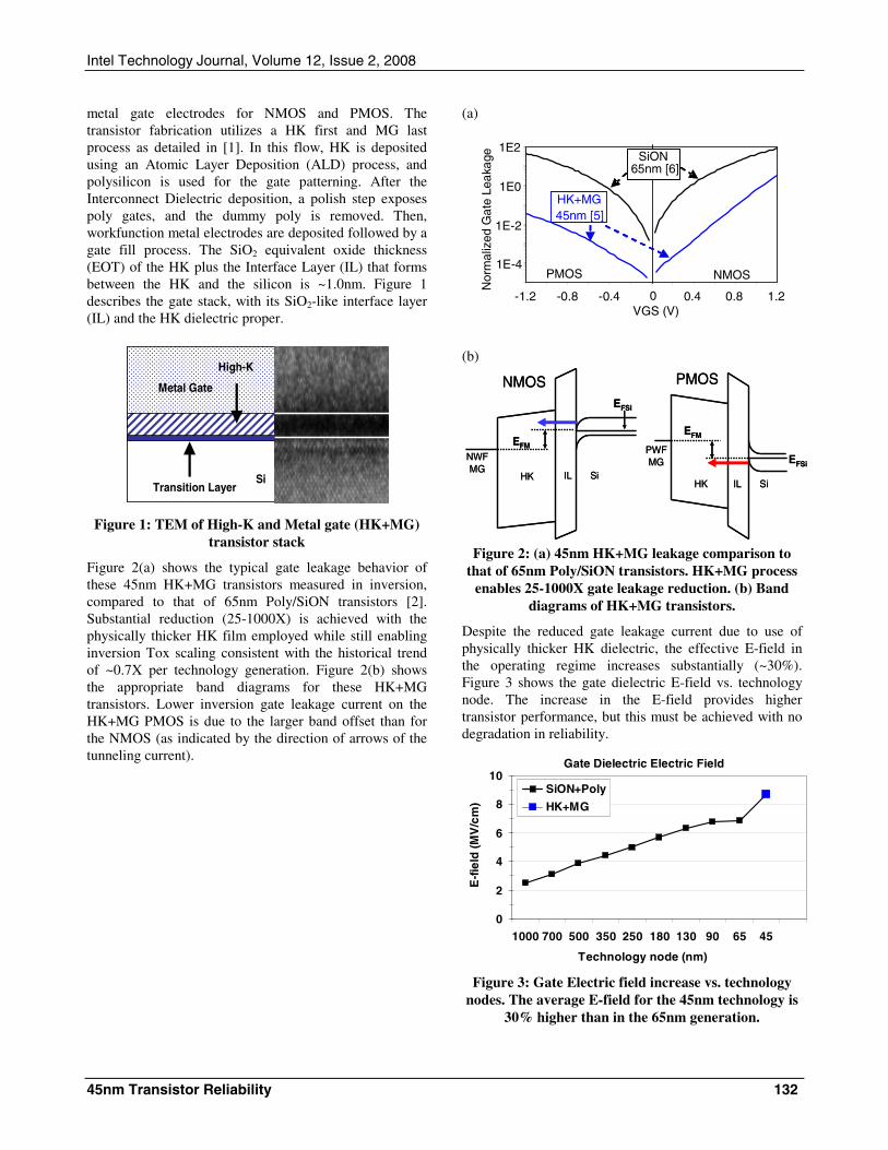
metal gate electrodes for NMOS and PMOS. The transistor fabrication utilizes a HK first and MG last process as detailed in [1]. In this flow, HK is deposited using an Atomic Layer Deposition (ALD) process, and polysilicon is used for the gate patterning. After the Interconnect Dielectric deposition, a polish step exposes poly gates, and the dummy poly is removed. Then, workfunction metal electrodes are deposited followed by a gate fill process. The SiO2 equivalent oxide thickness (EOT) of the HK plus the Interface Layer (IL) that forms between the HK and the silicon is ~1.0nm. Figure 1 describes the gate stack, with its SiO2-like interface layer (IL) and the HK dielectric proper.
Metal Gate
Transition LayerSi
High-K
Metal Gate
Transition LayerSi
High-K
Figure 1: TEM of High-K and Metal gate (HK+MG) transistor stack
Figure 2(a) shows the typical gate leakage behavior of these 45nm HK+MG transistors measured in inversion, compared to that of 65nm Poly/SiON transistors [2]. Substantial reduction (25-1000X) is achieved with the physically thicker HK film employed while still enabling inversion Tox scaling consistent with the historical trend of ~0.7X per technology generation. Figure 2(b) shows the appropriate band diagrams for these HK+MG transistors. Lower inversion gate leakage current on the HK+MG PMOS is due to the larger band offset than for the NMOS (as indicated by the direction of arrows of the tunneling current).
(a)
1E0
-1.2 -0.8 -0.4 0 0.4 0.8 1.2VGS (V)N
orm
aliz
ed G
ate
Leak
age
NMOS PMOS
SiON65nm [4]
HiK+MG45nm
1E2
1E-2
1E-4
1E0
-1.2 -0.8 -0.4 0 0.4 0.8 1.2VGS (V)N
orm
aliz
ed G
ate
Leak
age
NMOS PMOS
SiON65nm [5]
HiK+MG45nm
1E2
1E-2
1E-4
1E0
-1.2 -0.8 -0.4 0 0.4 0.8 1.2VGS (V)N
orm
aliz
ed G
ate
Leak
age
NMOS PMOS
SiON65nm [4]
HiK+MG45nm
1E2
1E-2
1E-4
1E0
-1.2 -0.8 -0.4 0 0.4 0.8 1.2VGS (V)
Nor
mal
ized
Gat
e Le
akag
e
NMOS PMOS
SiON65nm [6]
HK+MG45nm [5]
1E2
1E-2
1E-4
1E0
-1.2 -0.8 -0.4 0 0.4 0.8 1.2VGS (V)N
orm
aliz
ed G
ate
Leak
age
NMOS PMOS
SiON65nm [4]
HiK+MG45nm
1E2
1E-2
1E-4
1E0
-1.2 -0.8 -0.4 0 0.4 0.8 1.2VGS (V)N
orm
aliz
ed G
ate
Leak
age
NMOS PMOS
SiON65nm [5]
HiK+MG45nm
1E2
1E-2
1E-4
1E0
-1.2 -0.8 -0.4 0 0.4 0.8 1.2VGS (V)N
orm
aliz
ed G
ate
Leak
age
NMOS PMOS
SiON65nm [4]
HiK+MG45nm
1E2
1E-2
1E-4
1E0
-1.2 -0.8 -0.4 0 0.4 0.8 1.2VGS (V)
Nor
mal
ized
Gat
e Le
akag
e
NMOS PMOS
SiON65nm [6]
HK+MG45nm [5]
1E2
1E-2
1E-4
(b)
EFM
HK IL
NWFMG
EFM
EFSi
HK
PWFMG
NMOS PMOS
EFSi
SiIL Si
EFM
HK IL
NWFMG
EFM
EFSi
HK
PWFMG
NMOS PMOS
EFSi
SiIL Si
Figure 2: (a) 45nm HK+MG leakage comparison to
that of 65nm Poly/SiON transistors. HK+MG process enables 25-1000X gate leakage reduction. (b) Band
diagrams of HK+MG transistors.
Despite the reduced gate leakage current due to use of physically thicker HK dielectric, the effective E-field in the operating regime increases substantially (~30%). Figure 3 shows the gate dielectric E-field vs. technology node. The increase in the E-field provides higher transistor performance, but this must be achieved with no degradation in reliability.
Gate Dielectric Electric Field
0
2
4
6
8
10
1000 700 500 350 250 180 130 90 65 45
Technology node (nm)
E-f
ield
(MV
/cm
)
SiON+Poly
HK+MG
Figure 3: Gate Electric field increase vs. technology
nodes. The average E-field for the 45nm technology is 30% higher than in the 65nm generation.
The large increase in E-field with HK+MG contributes to the reliability challenges of this major technology transition. In the next section we provide background on the key reliability mechanisms that need to be considered in this transition.
TRANSISTOR RELIABILITY FUNDAMENTALS
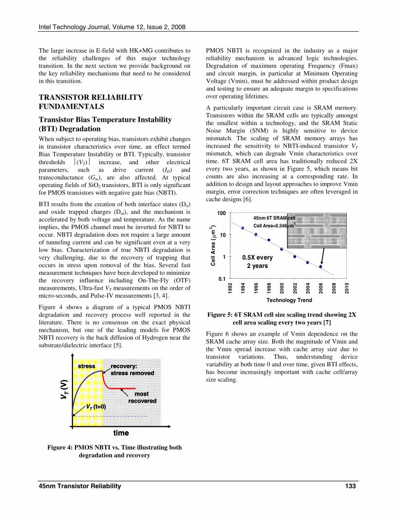
Transistor Bias Temperature Instability (BTI) Degradation When subject to operating bias, transistors exhibit changes in transistor characteristics over time, an effect termed Bias Temperature Instability or BTI. Typically, transistor thresholds ⏐(VT)⏐ increase, and other electrical parameters, such as drive current (ID) and transconductance (Gm), are also affected. At typical operating fields of SiO2 transistors, BTI is only significant for PMOS transistors with negative gate bias (NBTI).
BTI results from the creation of both interface states (Dit) and oxide trapped charges (Dot), and the mechanism is accelerated by both voltage and temperature. As the name implies, the PMOS channel must be inverted for NBTI to occur. NBTI degradation does not require a large amount of tunneling current and can be significant even at a very low bias. Characterization of true NBTI degradation is very challenging, due to the recovery of trapping that occurs in stress upon removal of the bias. Several fast measurement techniques have been developed to minimize the recovery influence including On-The-Fly (OTF) measurements, Ultra-fast VT measurements on the order of micro-seconds, and Pulse-IV measurements [3, 4].
Figure 4 shows a diagram of a typical PMOS NBTI degradation and recovery process well reported in the literature. There is no consensus on the exact physical mechanism, but one of the leading models for PMOS NBTI recovery is the back diffusion of Hydrogen near the substrate/dielectric interface [5].
time
VT
(V)
VT (t=0)
stress
most recovered
recovery:stress removed
time
VT
(V)
VT (t=0)
stress
most recovered
recovery:stress removed
Figure 4: PMOS NBTI vs. Time illustrating both degradation and recovery
PMOS NBTI is recognized in the industry as a major reliability mechanism in advanced logic technologies. Degradation of maximum operating Frequency (Fmax) and circuit margin, in particular at Minimum Operating Voltage (Vmin), must be addressed within product design and testing to ensure an adequate margin to specifications over operating lifetimes.
A particularly important circuit case is SRAM memory. Transistors within the SRAM cells are typically amongst the smallest within a technology, and the SRAM Static Noise Margin (SNM) is highly sensitive to device mismatch. The scaling of SRAM memory arrays has increased the sensitivity to NBTI-induced transistor VT mismatch, which can degrade Vmin characteristics over time. 6T SRAM cell area has traditionally reduced 2X every two years, as shown in Figure 5, which means bit counts are also increasing at a corresponding rate. In addition to design and layout approaches to improve Vmin margin, error correction techniques are often leveraged in cache designs [6].
0.1
1
10
100
1992
1994
1996
1998
2000
2002
2004
2006
2008
2010
Technology Trend
Cel
l Are
a ( μ
m2 )
0.5X every2 years
45nm 6T SRAM cell
Cell Area=0.346μm2
Figure 5: 6T SRAM cell size scaling trend showing 2X cell area scaling every two years [7]
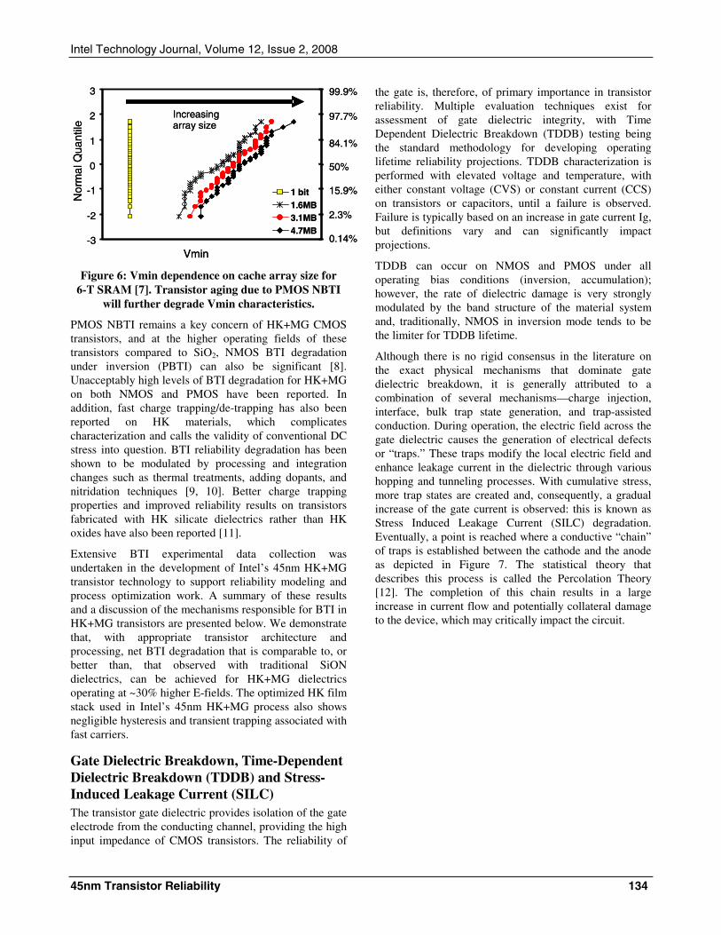
Figure 6 shows an example of Vmin dependence on the SRAM cache array size. Both the magnitude of Vmin and the Vmin spread increase with cache array size due to transistor variations. Thus, understanding device variability at both time 0 and over time, given BTI effects, has become increasingly important with cache cell/array size scaling.
Figure 6: Vmin dependence on cache array size for 6-T SRAM [7]. Transistor aging due to PMOS NBTI
will further degrade Vmin characteristics.
PMOS NBTI remains a key concern of HK+MG CMOS transistors, and at the higher operating fields of these transistors compared to SiO2, NMOS BTI degradation under inversion (PBTI) can also be significant [8]. Unacceptably high levels of BTI degradation for HK+MG on both NMOS and PMOS have been reported. In addition, fast charge trapping/de-trapping has also been reported on HK materials, which complicates characterization and calls the validity of conventional DC stress into question. BTI reliability degradation has been shown to be modulated by processing and integration changes such as thermal treatments, adding dopants, and nitridation techniques [9, 10]. Better charge trapping properties and improved reliability results on transistors fabricated with HK silicate dielectrics rather than HK oxides have also been reported [11].
Extensive BTI experimental data collection was undertaken in the development of Intel’s 45nm HK+MG transistor technology to support reliability modeling and process optimization work. A summary of these results and a discussion of the mechanisms responsible for BTI in HK+MG transistors are presented below. We demonstrate that, with appropriate transistor architecture and processing, net BTI degradation that is comparable to, or better than, that observed with traditional SiON dielectrics, can be achieved for HK+MG dielectrics operating at ~30% higher E-fields. The optimized HK film stack used in Intel’s 45nm HK+MG process also shows negligible hysteresis and transient trapping associated with fast carriers.
Gate Dielectric Breakdown, Time-Dependent Dielectric Breakdown (TDDB) and Stress-Induced Leakage Current (SILC) The transistor gate dielectric provides isolation of the gate electrode from the conducting channel, providing the high input impedance of CMOS transistors. The reliability of
the gate is, therefore, of primary importance in transistor reliability. Multiple evaluation techniques exist for assessment of gate dielectric integrity, with Time Dependent Dielectric Breakdown (TDDB) testing being the standard methodology for developing operating lifetime reliability projections. TDDB characterization is performed with elevated voltage and temperature, with either constant voltage (CVS) or constant current (CCS) on transistors or capacitors, until a failure is observed. Failure is typically based on an increase in gate current Ig, but definitions vary and can significantly impact projections.
TDDB can occur on NMOS and PMOS under all operating bias conditions (inversion, accumulation); however, the rate of dielectric damage is very strongly modulated by the band structure of the material system and, traditionally, NMOS in inversion mode tends to be the limiter for TDDB lifetime.
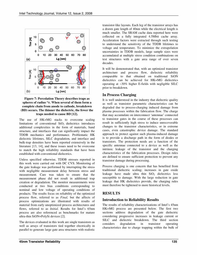
Although there is no rigid consensus in the literature on the exact physical mechanisms that dominate gate dielectric breakdown, it is generally attributed to a combination of several mechanisms—charge injection, interface, bulk trap state generation, and trap-assisted conduction. During operation, the electric field across the gate dielectric causes the generation of electrical defects or “traps.” These traps modify the local electric field and enhance leakage current in the dielectric through various hopping and tunneling processes. With cumulative stress, more trap states are created and, consequently, a gradual increase of the gate current is observed: this is known as Stress Induced Leakage Current (SILC) degradation. Eventually, a point is reached where a conductive “chain” of traps is established between the cathode and the anode as depicted in Figure 7. The statistical theory that describes this process is called the Percolation Theory [12]. The completion of this chain results in a large increase in current flow and potentially collateral damage to the device, which may critically impact the circuit.
Figure 7: Percolation Theory describes traps as spheres of radius “r. When several of them form a complete chain from anode to cathode, breakdown
(BD) occurs. The thinner the dielectric, the fewer the traps needed to cause BD [12].
The use of HK+MG stacks to overcome scaling limitations of conventional SiO2 dielectrics introduces additional complexities in the form of materials, band structure, and interfaces that can significantly impact the TDDB mechanics and performance. Problematic HK dielectric lifetimes, SILC degradation, and interface and bulk-trap densities have been reported extensively in the literature [13, 14], and these issues need to be overcome to match the high reliability standards that have been established with conventional dielectrics.
Unless specified otherwise, TDDB stresses reported in this work were carried out with DC CVS. Monitoring of the gate leakage was performed by interrupting the stress with negligible measurement delay between stress and measurement. Care was taken to ensure that the measurement phase did not result in additional trap creation or degradation. The monitor measurements were conducted at two bias conditions corresponding to nominal and low voltage of operating conditions of products. The results focus on reliability of the optimized process flow, referred to as Final, but the affects of process optimizations are illustrated with results of material from early unoptimized process architectures and flows, referred to as Initial. Results for Intel’s 65nm process are also referenced as benchmarks for mature ultra-thin SiON+PolySi devices [2].
The devices evaluated in this work are single transistors as well as arrays of transistors tied together electrically in parallel to generate large gate area structures with realistic
transistor-like layouts. Each leg of the transistor arrays has a drawn gate length of 40nm while the electrical length is much smaller. The SRAM cache data reported here were collected on a fully integrated 4.5Mbit cache array. Acceleration factors were extracted through such testing to understand the sensitivity of the TDDB lifetimes to voltage and temperature. To minimize the extrapolation uncertainties in TDDB models, large sample sizes were accumulated at multiple stress condition combinations on test structures with a gate area range of over seven decades.
It will be demonstrated that, with an optimized transistor architecture and process flow, dielectric reliability comparable to that obtained on traditional SiON dielectrics can be achieved for HK+MG dielectrics operating at ~30% higher E-fields with negligible SILC prior to breakdown.
In Process Charging It is well understood in the industry that dielectric quality as well as transistor parametric characteristics can be degraded due to process-charging induced damage from plasma processes within the fabrication flow. The charge that may accumulate on interconnect ‘antennae’ connected to transistor gates in the course of these processes can result in sufficiently high stress to induce unrecoverable changes to the transistor characteristics, or in extreme cases, even catastrophic device damage. The standard approach to protect against such plasma-induced damage is to provide a discharge path in the form of diodes or transistors. The protection needs are a function of the specific antennae connected to a device as well as the intrinsic leakage of the transistor and the charging characteristics of the fabrication processes. Design rules are defined to ensure sufficient protection to prevent any transistor damage during processing.
Process charging is one concern that has benefited from traditional dielectric scaling; increases in gate oxide leakage have made ultra thin SiO2 dielectrics less susceptible to damage. With the large reduction in gate leakage that HK dielectrics provide, the charging rules must therefore be tightened to more historical levels.
RESULTS
Introduction to Reliability Results The results of reliability characterizations of Intel’s 45nm HK+MG process are presented below. The first two sections address degradation of the gate dielectric considering progressive increases in leakage current or SILC and dielectric breakdown. The third section considers degradation in transistor operating characteristics due to charge trapping within the bulk of
the dielectric or at interfaces within the stack. The results reported here are for devices with the process minimum ‘drawn’ channel lengths of ~40nm, but devices spanning the permitted layout range were evaluated with similar results. Unless stated otherwise, the data below are for devices on the optimized 45nm HK+MG process flow. Some results from 45nm development process flows as well as for a mature 65nm process are shown for comparative purposes.
Dielectric Reliability Transistor dielectric reliability was assessed for a wide range of transistor structures ranging from single cache bitcell transistors to 4.5Mb SRAM cache test vehicles. Conventional CVS was employed unless otherwise indicated.
Dielectric Reliability—TDDB TDDB is associated with a substantial increase in current through the transistor dielectric. In the data below, the definition of failure for extraction of TDDB lifetimes is the point where an abrupt increase in dielectric current is observed or a “hard breakdown” (HBD) occurs. This increase in current due to HBD may be sufficient to, but won’t necessarily, result in circuit failure.
Figure 8 compares matched Electric field TDDB on SiON+PolySi vs. the optimized Intel 45nm HK+MG gate [15].
1.E+00
1.E+01
1.E+02
1.E+03
1.E+04
1.E+05
1.E+06
1.E+07
1.E+08
1.E+09
1.E+10
6 8 10 12 14 16Field (MV/cm)
TD
DB
(sec
)
65nmSiON
45nmHK-MG
Figure 8: TDDB vs. Electric field comparison of HK+MG [1] and SiON [2] showing that an optimized HK+MG dielectric can support 30% higher field than a mature SiON-based technology at matched TDDB
lifetime
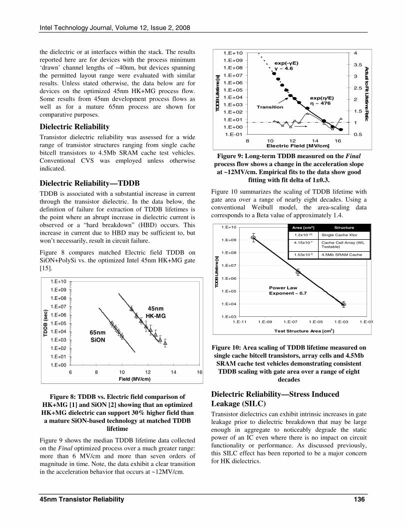
Figure 9 shows the median TDDB lifetime data collected on the Final optimized process over a much greater range: more than 6 MV/cm and more than seven orders of magnitude in time. Note, the data exhibit a clear transition in the acceleration behavior that occurs at ~12MV/cm.
1.E-01
1.E+00
1.E+01
1.E+02
1.E+03
1.E+04
1.E+05
1.E+06
1.E+07
1.E+08
1.E+09
1.E+10
8 10 12 14 16Electric Field [MV/cm]
TDDB L
ifet
ime
[s]
0.5
1
1.5
2
2.5
3
3.5
4
Actu
al to F
it Lifetim
e Ratio
exp(-γE)γ ~ 4.6
exp(η/E)η ~ 476
Transition
Figure 9: Long-term TDDB measured on the Final
process flow shows a change in the acceleration slope at ~12MV/cm. Empirical fits to the data show good
fitting with fit delta of 1±0.3.
Figure 10 summarizes the scaling of TDDB lifetime with gate area over a range of nearly eight decades. Using a conventional Weibull model, the area-scaling data corresponds to a Beta value of approximately 1.4.
1.E+03
1.E+04
1.E+05
1.E+06
1.E+07
1.E+08
1.E+09
1.E+10
1.E-11 1.E-09 1.E-07 1.E-05 1.E-03 1.E-01
Test Structure Area [cm2]
TD
DB
Lifet
ime
[s]
Power Law Exponent ~ 0.7
4.5Mb SRAM Cache1.53x10-3
Cache Cell Array (WL Testable)
4.15x10⁻⁷
Single Cache Xtor1.2x10-10
StructureArea [cm2]
4.5Mb SRAM Cache1.53x10-3
Cache Cell Array (WL Testable)
4.15x10⁻⁷
Single Cache Xtor1.2x10-10
StructureArea [cm2]
Figure 10: Area scaling of TDDB lifetime measured on single cache bitcell transistors, array cells and 4.5Mb SRAM cache test vehicles demonstrating consistent TDDB scaling with gate area over a range of eight
decades
Dielectric Reliability—Stress Induced Leakage (SILC) Transistor dielectrics can exhibit intrinsic increases in gate leakage prior to dielectric breakdown that may be large enough in aggregate to noticeably degrade the static power of an IC even where there is no impact on circuit functionality or performance. As discussed previously, this SILC effect has been reported to be a major concern for HK dielectrics.
Figure 11 compares early time evolution of Ig under inversion stress of NMOS devices fabricated with an early, unoptimized 45nm HK+MG process flow to that of material from the Final optimized process flow and for a conventional SiON stack.
1.E-08
1.E-07
1.E-06
1.E-05
1.E-04
1.E-03
1.E-02
1.E-01
1.E+00
1.E+00 1.E+01 1.E+02 1.E+03 1.E+04 1.E+05 1.E+06
Time [s]
NM
OS
Lea
kag
e [A
]
SiON (Ref [4])
Final
Initial
E ~ 11MV/cm for all data
Figure 11. SILC degradation on Initial vs. Final process flows demonstrates improvement through process optimization. The SiO2 case is shown for reference and exhibits relatively negligible SILC
degradation as expected. The Final process exhibits similar levels of SILC degradation as observed on the
SiO2 reference.
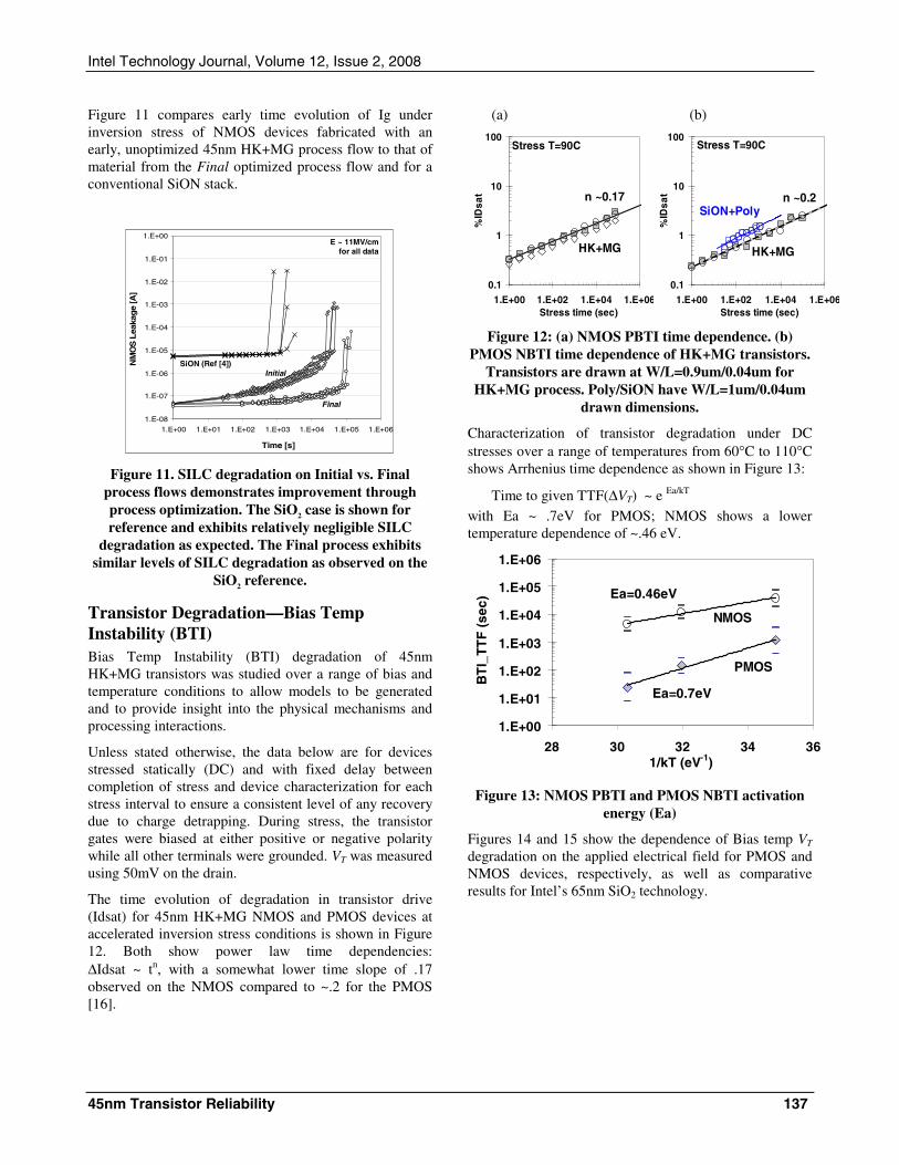
Transistor Degradation—Bias Temp Instability (BTI) Bias Temp Instability (BTI) degradation of 45nm HK+MG transistors was studied over a range of bias and temperature conditions to allow models to be generated and to provide insight into the physical mechanisms and processing interactions.
Unless stated otherwise, the data below are for devices stressed statically (DC) and with fixed delay between completion of stress and device characterization for each stress interval to ensure a consistent level of any recovery due to charge detrapping. During stress, the transistor gates were biased at either positive or negative polarity while all other terminals were grounded. VT was measured using 50mV on the drain.
The time evolution of degradation in transistor drive (Idsat) for 45nm HK+MG NMOS and PMOS devices at accelerated inversion stress conditions is shown in Figure 12. Both show power law time dependencies: ΔIdsat ~ tn, with a somewhat lower time slope of .17 observed on the NMOS compared to ~.2 for the PMOS [16].
(a) (b)
0.1
1
10
100
1.E+00 1.E+02 1.E+04 1.E+06Stress time (sec)
%ID
sat n ~0.2
HK+MG
SiON+Poly
Stress T=90C
n ~0.17
0.1
1
10
100
1.E+00 1.E+02 1.E+04 1.E+06Stress time (sec)
%ID
sat
Stress T=90C
HK+MG
Figure 12: (a) NMOS PBTI time dependence. (b)
PMOS NBTI time dependence of HK+MG transistors. Transistors are drawn at W/L=0.9um/0.04um for
HK+MG process. Poly/SiON have W/L=1um/0.04um drawn dimensions.
Characterization of transistor degradation under DC stresses over a range of temperatures from 60°C to 110°C shows Arrhenius time dependence as shown in Figure 13:
Time to given TTF(ΔVT) ~ e Ea/kT with Ea ~ .7eV for PMOS; NMOS shows a lower temperature dependence of ~.46 eV.
1.E+00
1.E+01
1.E+02
1.E+03
1.E+04
1.E+05
1.E+06
28 30 32 34 361/kT (eV-1)
BT
I_T
TF
(se
c)
Ea=0.46eV
Ea=0.7eV
PMOS
NMOS
Figure 13: NMOS PBTI and PMOS NBTI activation energy (Ea)
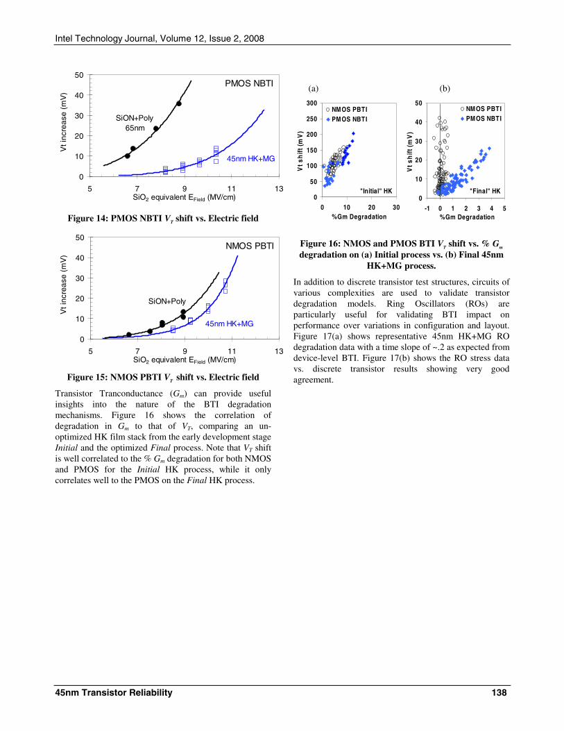
Figures 14 and 15 show the dependence of Bias temp VT degradation on the applied electrical field for PMOS and NMOS devices, respectively, as well as comparative results for Intel’s 65nm SiO2 technology.
Transistor Tranconductance (Gm) can provide useful insights into the nature of the BTI degradation mechanisms. Figure 16 shows the correlation of degradation in Gm to that of VT, comparing an un-optimized HK film stack from the early development stage Initial and the optimized Final process. Note that VT shift is well correlated to the % Gm degradation for both NMOS and PMOS for the Initial HK process, while it only correlates well to the PMOS on the Final HK process.
(a) (b)
Figure 16: NMOS and PMOS BTI VT shift vs. % Gm degradation on (a) Initial process vs. (b) Final 45nm
HK+MG process.
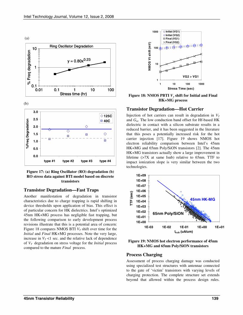
In addition to discrete transistor test structures, circuits of various complexities are used to validate transistor degradation models. Ring Oscillators (ROs) are particularly useful for validating BTI impact on performance over variations in configuration and layout. Figure 17(a) shows representative 45nm HK+MG RO degradation data with a time slope of ~.2 as expected from device-level BTI. Figure 17(b) shows the RO stress data vs. discrete transistor results showing very good agreement.
Figure 17: (a) Ring Oscillator (RO) degradation (b) RO stress data against BTI model based on discrete
transistors
Transistor Degradation—Fast Traps Another manifestation of degradation in transistor characteristics due to charge trapping is rapid shifting in device thresholds upon application of bias. This effect is of particular concern for HK dielectrics. Intel’s optimized 45nm HK+MG process has negligible fast trapping, but the following comparison to early development process revisions illustrate that this is a potential area of concern: Figure 18 compares NMOS BTI VT shift over time for the Initial and Final HK+MG processes. Note the very large, increase in VT <1 sec. and the relative lack of dependence of VT degradation on stress voltage for the Initial process compared to the mature Final process.
1
10
100
1000
1 10 100 1000
Stress Time (sec)
NM
OS
Vt s
hift
(mV
)
Initial (VG1)Initial (VG2)Final (VG1)Final (VG2)
VG2 > VG1
Figure 18: NMOS PBTI VT shift for Initial and Final
HK+MG process
Transistor Degradation—Hot Carrier Injection of hot carriers can result in degradation in VT and Gm. The low conduction band offset for Hf-based HK dielectric in contact with a silicon substrate results in a reduced barrier, and it has been suggested in the literature that this poses a potentially increased risk for the hot carrier injection [17]. Figure 19 shows NMOS hot electron reliability comparison between Intel’s 45nm HK+MG and 65nm Poly/SiON transistors [2]. The 45nm HK+MG transistors actually show a large improvement in lifetime (>7X at same Isub) relative to 65nm. TTF to impact ionization slope is very similar between the two technologies.
1E+00
1E+01
1E+02
1E+03
1E+04
1E+05
1E+06
1E+07
1E+08
1E+09
1E-03 1E-02 1E-01 1E+00 1E+01Isub (uA/um)
TT
F (s
ec)
65nm Poly/SiON
45nm HK-MG
Figure 19: NMOS hot electron performance of 45nm HK+MG and 65nm Poly/SiON transistors
Process Charging Assessment of process charging damage was conducted using specialized test structures with antennae connected to the gate of ‘victim’ transistors with varying levels of charging protection. The complete structure set extends beyond that allowed within the process design rules.
Transistor parametric characteristics at the completion of processing are monitored on these structures, and transistor reliability stresses are conducted and compared to reference devices with no antennae. These results confirm no charging degradation on devices compliant to design rule protection requirements.
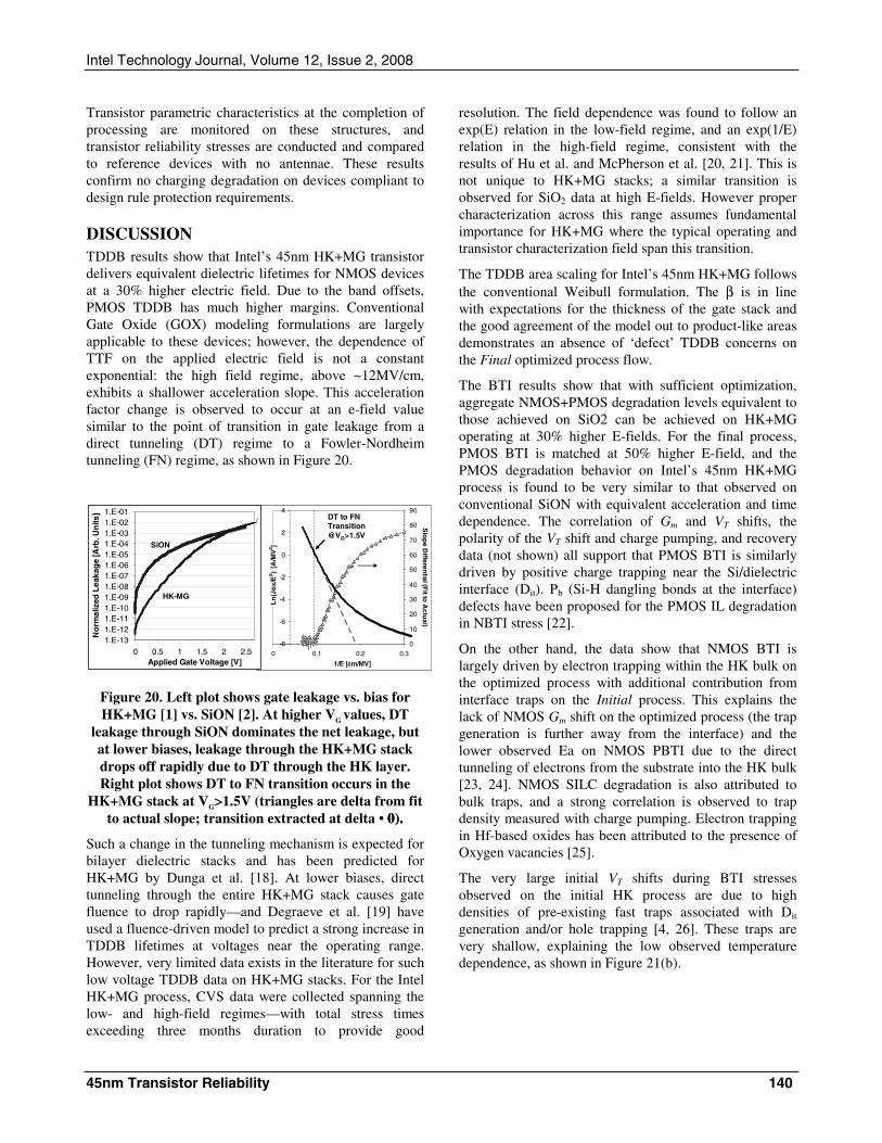
DISCUSSION TDDB results show that Intel’s 45nm HK+MG transistor delivers equivalent dielectric lifetimes for NMOS devices at a 30% higher electric field. Due to the band offsets, PMOS TDDB has much higher margins. Conventional Gate Oxide (GOX) modeling formulations are largely applicable to these devices; however, the dependence of TTF on the applied electric field is not a constant exponential: the high field regime, above ~12MV/cm, exhibits a shallower acceleration slope. This acceleration factor change is observed to occur at an e-field value similar to the point of transition in gate leakage from a direct tunneling (DT) regime to a Fowler-Nordheim tunneling (FN) regime, as shown in Figure 20.
Figure 20. Left plot shows gate leakage vs. bias for HK+MG [1] vs. SiON [2]. At higher VG values, DT
leakage through SiON dominates the net leakage, but at lower biases, leakage through the HK+MG stack drops off rapidly due to DT through the HK layer. Right plot shows DT to FN transition occurs in the
HK+MG stack at VG>1.5V (triangles are delta from fit to actual slope; transition extracted at delta • 0). 0).
Such a change in the tunneling mechanism is expected for bilayer dielectric stacks and has been predicted for HK+MG by Dunga et al. [18]. At lower biases, direct tunneling through the entire HK+MG stack causes gate fluence to drop rapidly—and Degraeve et al. [19] have used a fluence-driven model to predict a strong increase in TDDB lifetimes at voltages near the operating range. However, very limited data exists in the literature for such low voltage TDDB data on HK+MG stacks. For the Intel HK+MG process, CVS data were collected spanning the low- and high-field regimes—with total stress times exceeding three months duration to provide good
resolution. The field dependence was found to follow an exp(E) relation in the low-field regime, and an exp(1/E) relation in the high-field regime, consistent with the results of Hu et al. and McPherson et al. [20, 21]. This is not unique to HK+MG stacks; a similar transition is observed for SiO2 data at high E-fields. However proper characterization across this range assumes fundamental importance for HK+MG where the typical operating and transistor characterization field span this transition.
The TDDB area scaling for Intel’s 45nm HK+MG follows the conventional Weibull formulation. The β is in line with expectations for the thickness of the gate stack and the good agreement of the model out to product-like areas demonstrates an absence of ‘defect’ TDDB concerns on the Final optimized process flow.
The BTI results show that with sufficient optimization, aggregate NMOS+PMOS degradation levels equivalent to those achieved on SiO2 can be achieved on HK+MG operating at 30% higher E-fields. For the final process, PMOS BTI is matched at 50% higher E-field, and the PMOS degradation behavior on Intel’s 45nm HK+MG process is found to be very similar to that observed on conventional SiON with equivalent acceleration and time dependence. The correlation of Gm and VT shifts, the polarity of the VT shift and charge pumping, and recovery data (not shown) all support that PMOS BTI is similarly driven by positive charge trapping near the Si/dielectric interface (Dit). Pb (Si-H dangling bonds at the interface) defects have been proposed for the PMOS IL degradation in NBTI stress [22].
On the other hand, the data show that NMOS BTI is largely driven by electron trapping within the HK bulk on the optimized process with additional contribution from interface traps on the Initial process. This explains the lack of NMOS Gm shift on the optimized process (the trap generation is further away from the interface) and the lower observed Ea on NMOS PBTI due to the direct tunneling of electrons from the substrate into the HK bulk [23, 24]. NMOS SILC degradation is also attributed to bulk traps, and a strong correlation is observed to trap density measured with charge pumping. Electron trapping in Hf-based oxides has been attributed to the presence of Oxygen vacancies [25].
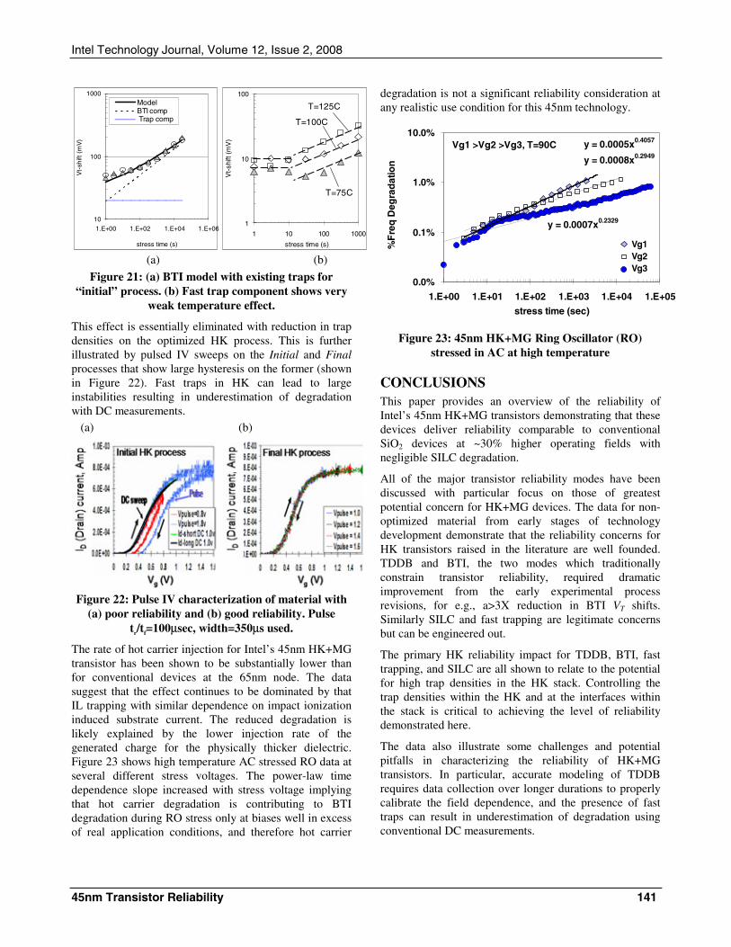
The very large initial VT shifts during BTI stresses observed on the initial HK process are due to high densities of pre-existing fast traps associated with Dit generation and/or hole trapping [4, 26]. These traps are very shallow, explaining the low observed temperature dependence, as shown in Figure 21(b).
Figure 21: (a) BTI model with existing traps for “initial” process. (b) Fast trap component shows very
weak temperature effect.
This effect is essentially eliminated with reduction in trap densities on the optimized HK process. This is further illustrated by pulsed IV sweeps on the Initial and Final processes that show large hysteresis on the former (shown in Figure 22). Fast traps in HK can lead to large instabilities resulting in underestimation of degradation with DC measurements. (a) (b)
Figure 22: Pulse IV characterization of material with
(a) poor reliability and (b) good reliability. Pulse tr/tf=100μsec, width=350μs used.
The rate of hot carrier injection for Intel’s 45nm HK+MG transistor has been shown to be substantially lower than for conventional devices at the 65nm node. The data suggest that the effect continues to be dominated by that IL trapping with similar dependence on impact ionization induced substrate current. The reduced degradation is likely explained by the lower injection rate of the generated charge for the physically thicker dielectric. Figure 23 shows high temperature AC stressed RO data at several different stress voltages. The power-law time dependence slope increased with stress voltage implying that hot carrier degradation is contributing to BTI degradation during RO stress only at biases well in excess of real application conditions, and therefore hot carrier
degradation is not a significant reliability consideration at any realistic use condition for this 45nm technology.
y = 0.0005x0.4057
y = 0.0008x0.2949
y = 0.0007x0.2329
0.0%
0.1%
1.0%
10.0%
1.E+00 1.E+01 1.E+02 1.E+03 1.E+04 1.E+05
stress time (sec)
%F
req
Deg
rad
atio
n
1.8V1.5V1.4V
Vg1Vg2Vg3
Vg1 >Vg2 >Vg3, T=90C
Figure 23: 45nm HK+MG Ring Oscillator (RO) stressed in AC at high temperature
CONCLUSIONS This paper provides an overview of the reliability of Intel’s 45nm HK+MG transistors demonstrating that these devices deliver reliability comparable to conventional SiO2 devices at ~30% higher operating fields with negligible SILC degradation.
All of the major transistor reliability modes have been discussed with particular focus on those of greatest potential concern for HK+MG devices. The data for non-optimized material from early stages of technology development demonstrate that the reliability concerns for HK transistors raised in the literature are well founded. TDDB and BTI, the two modes which traditionally constrain transistor reliability, required dramatic improvement from the early experimental process revisions, for e.g., a>3X reduction in BTI VT shifts. Similarly SILC and fast trapping are legitimate concerns but can be engineered out.
The primary HK reliability impact for TDDB, BTI, fast trapping, and SILC are all shown to relate to the potential for high trap densities in the HK stack. Controlling the trap densities within the HK and at the interfaces within the stack is critical to achieving the level of reliability demonstrated here.
The data also illustrate some challenges and potential pitfalls in characterizing the reliability of HK+MG transistors. In particular, accurate modeling of TDDB requires data collection over longer durations to properly calibrate the field dependence, and the presence of fast traps can result in underestimation of degradation using conventional DC measurements.
The overriding message is that although the revolutionary change represented by HK+MG poses daunting reliability challenges, these can all be addressed with appropriate transistor architecture and process optimizations, delivering the same reliability as conventional SiO2 devices with compelling power/performance advantages.
ACKNOWLEDGMENTS M. Agostinelli, M. Brazier, R. Chau, G. Dewey, T. Ghani, J. Kavalieros, K. Kuhn, M. Kuhn, M. Metz, K. Mistry, S. Ramey, A. Roskowski, J. Sandford, C. Thomas, J. Thomas, C. Wiegand, and J. Wiedemer.
REFERENCES [1] K. Mistry et al., “A 45nm Logic Technology with
High-k + Metal Gate Transistors, Strained Silicon, 9 Cu Interconnect Layers, 193nm Dry Patterning, and 100% Pb-free Packaging.” In IEDM Technology Digest, 2007.
[2] P. Bai et al., “A 65 nm Logic Technology Featuring 35nm Gate Lengths, Enhanced Channel Strain, 8 Cu Interconnect Layers, Low-k ILD, and 0.57um2 SRAM Cell.” In IEDM Technology Digest, 2004, pp. 657–660.
[3] J. Mitard et al., “Large-Scale Time Characterization and Analysis of PBTI in HfO2/Metal Gate Stacks.” In Proceedings of International Reliability Physics Symposium, 2006, pp. 174–178.
[4] H. Reisinger et al., “A Comparison of Very Fast to Very Slow Components in Degradation and Recovery Due to NBTI and Bulk Hole Trapping to Existing Physical Models.” IEEE Transactions on Device and Materials Reliability, vol. 7, no. 1, 2007, pp. 119–129.
[5] M. Alam et al., “A Critical Examination of the Mechanics of Dynamic NBTI for PMOSFETs.” In IEDM Technology Digest 2003, pp. 345–348.
[6] A. Agarwal et al., “A Process-Tolerant Cache Architecture for Improved Yield in Nanoscale Technologies.” IEEE Transactions on VLSI, vol. 13, no. 1, January 2005, pp. 27–38.
[7] J. Maiz, “Reliability Challenges: Preventing Them from Becoming Limiters to Technology Scaling.” In Proceedings of International Integrated Reliability Workshop, Invited talk, 2006.
[8] G. Bersuker et al., “Mechanism of Electron Trapping and Characteristics of Traps in HfO2 Gate Stacks.” IEEE Transactions on Device and Materials Reliability, vol. 7, no. 1, 2007, pp. 138–145.
[9] M. Houssa et al., “Detrimental Impact of Hydrogen on Negative Bias Temperature Instabilities in HfO2-based
pMOSFETs.” In Symposium on VLSI Technology Digest 2004, pp. 212–213.
[10]G. Wilk et al., “High-k gate dielectrics: Current status and materials properties considerations,” Journal of Applied Physics, vol. 89, no. 10, 2001, pp. 5243–5275.
[11]A. Shanware et al., “Characterization and Comparison of the Charge Trapping in HfSiON and HfO2 Gate Dielectrics.” In IEDM Technology Digest, pp. 939–942, 2003.
[12] J. H. Stathis, “Percolation models for gate oxide breakdown.” Journal of Applied Physics, vol. 86, no. 10, 1999, pp. 5757–5766.
[13] S. C. Song et al., “Highly Manufacturable 45nm LSTP CMOSFETs Using Novel Dual High-k and Dual Metal Gate CMOS Integration.” In Symposium on VLSI Technology Digest, 2006, pp. 13–14.
[14] G. Ribes et al., “Review on High-k Dielectrics Reliability Issues.” IEEE Transactions on Device and Materials Reliability, vol. 5, no. 1, 2005, pp. 5–19.
[15]C. Prasad et al., “Dielectric Breakdown in a 45 nm High-K/Metal Gate Process Technology.” In Press: in Proceedings of International Reliability Physics Symposium, 2008.
[16]S. Pae et al., “BTI Reliability of 45 nm High-K + Metal-Gate Process Technology.” In Press: in Proceedings of International Reliability Physics Symposium, 2008.
[17]H. Park et al., “Decoupling of Cold-Carrier Effects in Hot-Carrier Reliability Assessment of bHfO2 Gated nMOSFETs.” IEEE Electron Device Letters, vol. 27, no. 8, 2006, pp. 662–664.
[18] M. V. Dunga et al., ”Modeling of Direct Tunneling Current in Multi-layer Gate Stacks.” Nanotechnology 2003, vol. 2, pp. 306–309.
[19] R. Degraeve et al., ”Stress Polarity Dependence of Degradation and Breakdown of SiO2/High-K Stacks.” In Proceedings of International Reliability Physics Symposium, 2003, pp. 23–28.
[20] C. Hu et al., “A Unified Gate Oxide Reliability Model.” in Proceedings of International Reliability Physics Symposium, 1999, pp. 47–51.
[21] J. W. McPherson et al., “Trends in the Ultimate Breakdown Strength of High Dielectric-Constant Materials.” IEEE Transactions On Electron Devices, vol. 50, no. 8, 2003, pp. 1771–1778.
[22] M. Houssa et el., “Reaction-dispersive proton transport model for negative bias temperature
[23] G. Ribes et al., “Review on High-k Dielectrics Reliability Issues.” IEEE Transactions on Device and Materials Reliability, vol. 5, no. 1, 2005, pp. 5–19.
[24] S. Kalpat et al., “BTI Characteristics and Mechanisms of Metal Gated HfO2 Films with Enhanced Interface/Bulk Process Treatments.” IEEE Transactions on Device and Materials Reliability, vol. 5, no. 1, 2005, pp. 26–35.
[25] A. Kang et al., “Electron spin resonance observation of trapped electron centers in atomic-layer-deposited hafnium oxide on Si.” Applied Physics Letters, vol. 83, no. 16, 2003, pp. 3407–3409.
[26] V. Huard et al., “New characterization and modeling approach for NBTI degradation from transistor to product level.” In IEDM Technology Digest, 2007.
AUTHORS’ BIOGRAPHIES Jeffrey Hicks is a Senior Principle Engineer in Intel’s Technology Development Quality and Reliability Group and was the Q&R Program Manager for Intel’s 45nm HK+MG technology. He received his B.S. degree in Applied Physics from Caltech in 1980 and joined Intel’s Technology Development Group in Santa Clara CA in that year as a Reliability Engineer working on Bipolar and EPROM non-volatile memory technologies. In his years at Intel to date Mr. Hicks has served in numerous Quality and Reliability functions spanning Technology Development, Manufacturing, Product, and Customer Quality and Reliability. He has several patents received or pending and has published a number of technical papers including Best Paper at the 1999 International Reliability Physics Symposium. He is the recipient of three Intel Achievement Awards. His e-mail is Jeffrey.Hicks at intel.com.
Daniel Bergstrom is a Group Leader for front-end metals deposition in Intel’s Portland Technology Development Group. He has been with Intel since 1997 and has worked on metal deposition technologies stretching from 0.25μm down to his current work on 32nm technology. He received a B.S. degree in Ceramic Engineering from the University of Illinois in 1992 and a Ph.D. degree in Materials Science from the University of Illinois in 1997. His e-mail is daniel.bergstrom at intel.com.
Michael Hattendorf is a Process Integration Engineer working in Intel’s Portland Technology Development Group. He has been with Intel since 2002 and has focused on 45nm transistor yield, performance, and reliability for the last four years. He received B.S., M.S., and Ph.D. degrees in Electrical Engineering from the University of
Illinois at Urbana-Champaign. His e-mail is michael.l.hattendorf at intel.com.
Jason Jopling is a Quality and Reliability Engineer in Intel’s Logic Technology Development Group working primarily on memory and transistor reliability. His interests include process- and device-level impacts on quality/reliability of integrated memories, circuits, and products. He holds dual B.S. degrees in Biomedical and Electrical Engineering from the University of Southern California and M.S. and Ph.D. degrees in Electrical Engineering from Duke University. His e-mail is jason.jopling at intel.com.
Jose Maiz is an Intel Fellow and Director of Logic Technology Quality and Reliability. He joined Intel in 1983 and became a Fellow in 2002. He is presently responsible for identification of silicon reliability limiters to scaling and their resolution for Intel's next-generation silicon technologies and logic products. Dr. Maiz graduated with a degree in Physics from the University of Navarra in San Sebastian in 1976. He then moved to the U.S., graduating with M.S. and Ph.D. degrees in Electrical Engineering from Ohio State University in 1980 and 1983, respectively. In 1983 he joined Intel Corporation where he has contributed in various management and individual contributor roles to more than 10 silicon technology generations in the areas of quality and reliability. Maiz holds 9 patents and has 13 more pending. He has authored or co-authored over 35 publications and conference presentations, a number of them invited including keynote addresses at the 2007 IRW and MRQW conferences. He is a recipient of an Intel Achievement Award and numerous divisional recognition awards. He was also a Fulbright Scholar in 1978. He is a senior member of the IEEE. His e-mail is Jose.Maiz at intel.com.
Sangwoo Pae received a B.S.E.E. degree from the Chung-Ang University in Korea (1994) and M.S. and Ph.D. degrees in 1996 and 1999, respectively, in ECE from Purdue University in West Lafayette, IN. He has been with Intel since 2000 in the Logic Technology and Development Quality and Reliability Group in Oregon. He has contributed to the development and reliability of Intel’s 130nm, 90nm, and 45nm technology and recently has worked on 32nm logic technology nodes. He is currently a Sr. Staff QRE. He has authored/co-authored over 20 publications and holds 2 patents with 9 more pending. His e-mail is Sangwoo.pae at intel.com.
Chetan Prasad received his B.E. degree from the University of Mumbai in 1997 with an emphasis on Electronics and Telecommunications. He received his M.S. degree in 1999 and his Ph.D. degree in 2003 from Arizona State University, where his research focused on non-equilibrium carrier dynamics and relaxation in III-V semiconductor nanostructures. He joined Intel
Corporation in 2003 and is currently a Senior Reliability Engineer with Intel’s Technology Development Quality and Reliability Group. His responsibilities include research in transistor reliability and dielectric wear-out mechanisms for Intel’s advanced process technologies. He has contributed to Intel’s 65nm and 45nm technologies and is currently working on enhancement activities on the 45nm technology node. Chetan has authored/co-authored over 30 papers published in peer-reviewed journals and conference proceedings and has 2 patents pending. He has received an Intel Achievement Award and an LTD Divisional Award. His e-mail is chetan.prasad at intel.com.
Jami Wiedemer is a Device Engineer in Intel’s Portland Technology Development Group. She joined Intel in 2005 and has focused on electrical properties of high-k gate dielectrics and their impact on 45nm transistor performance. She is currently working on pathfinding for 22nm process technology. She received M.S. and Ph.D. degrees in Electrical Engineering from Cornell University and a B.S. degree in Electrical Engineering from the University of Notre Dame. Her e-mail is jami.a.wiedemer at intel.com.
BunnyPeople, Celeron, Celeron Inside, Centrino, Centrino logo, Core Inside, FlashFile, i960, InstantIP, Intel, Intel logo, Intel386, Intel486, Intel740, IntelDX2, IntelDX4, IntelSX2, Intel Core, Intel Inside, Intel Inside logo, Intel. Leap ahead., Intel. Leap ahead. logo, Intel NetBurst, Intel NetMerge, Intel NetStructure, Intel SingleDriver, Intel SpeedStep, Intel StrataFlash, Intel Viiv, Intel vPro, Intel XScale, IPLink, Itanium, Itanium Inside, MCS, MMX, Oplus, OverDrive, PDCharm, Pentium, Pentium Inside, skoool, Sound Mark, The Journey Inside, VTune, Xeon, and Xeon Inside are trademarks or registered trademarks of Intel Corporation or its subsidiaries in the United States and other countries.
Intel's trademarks may be used publicly with permission only from Intel. Fair use of Intel's trademarks in advertising and promotion of Intel products requires proper acknowledgement.
*Other names and brands may be claimed as the property of others.
Microsoft, Windows, and the Windows logo are trademarks, or registered trademarks of Microsoft Corporation in the United States and/or other countries.
Bluetooth is a trademark owned by its proprietor and used by Intel Corporation under license.
Intel Corporation uses the Palm OS® Ready mark under license from Palm, Inc.
LEED - Leadership in Energy & Environmental Design (LEED®)