24
DAC 2006 Reliability Challenges for 45nm and Beyond J. W. McPherson, PhD, TI Senior Fellow Texas Instruments, Inc. Dallas, Texas 75243 1

DAC 2006
Reliability Challengesfor 45nm and Beyond
J. W. McPherson, PhD, TI Senior FellowTexas Instruments, Inc.
Dallas, Texas 75243
1

Outline
Transistor Performance with Scaling
Gate Dielectric Scaling
Interconnect Scaling
Reliability Trends with Continued Scaling--- Leakage --- NBTI --- ESD --- SM--- TDDB --- CHC --- EM --- Joule Heating
Defect Issues with Continued Scaling
Conclusions/Summary2

Lightly Doped Drain (LDD)Channel Region
Source/Drain
Sidewall Spacer
Polysilicon GateGate Oxide
SalicideCladding
SiliconSubstrate
GATESOURCE DRAIN
MOSFET Scaling : More Evolutionary than Revolutionary for 25 years3
LighlyDoped Drain (LDD)
Channel Region
Source/Drain
SidewallSpacerPolysiliconGate
Gate Oxide
SalicideCladding
SiliconSubstrate
MOSFET Scaling: More Evolutionary than Revolutionary
( )ddctInterconneGateJunction
drive
VCCCIFOM++
=

1.00E-14
1.00E-12
1.00E-10
1.00E-08
1.00E-06
1.00E-04
1.00E-02
-0.2 0 0.2 0.4 0.6 0.8 1 1.2
Vgs (V)
Ids
(A)
Subthreshold slope remains nearly constant fromtechnology node to node:
Vt must be reduced to maintain good Idrive at lower Vdd
Ioff increases with lower Vt due to constant subthreshold slope
Transistor Idrive Versus Ioff Trends
Increased transistor Idrive usually implies increased Ioff 4

Strained-Silicon Performance Enhancement
Raised S/D
PMD liner
STI linerImplant S/D strain
Recess S/D epi
Active area epi Substrate
orientation
Capped poly
Strainedchannel
Normal Si lattice Strained Si lattice Improved mobility
Raised S/D
PMD liner
STI linerImplant S/D strain
Recess S/D epi
Active area epi Substrate
orientation
Capped poly
Strainedchannel
Normal Si lattice Strained Si lattice Improved mobility
Significant Ion/Ioff improvement
1. Strained Si can produce an increase in Ionwithout a degradation in Ioff.
2. Stress-induced defects can occur in the silicon if the stress is not applied properly.
Defect in Silicon
-6
Ioff
log
(A/μ
m)
Ion (μA/μm)
35 % improvement
40 nA/μm
680 μA/μm-10
-9
-8
-7
300 500 700
ReferenceSiGe
-6
Ioff
log
(A/μ
m)
Ion (μA/μm)
35 % improvement
40 nA/μm
680 μA/μm-10
-9
-8
-7
300 500 700
ReferenceSiGe
Ioff
log
(A/μ
m)
Ion (μA/μm)
35 % improvement
40 nA/μm
680 μA/μm-10-10
-9
-8
-7
300 500 700
ReferenceSiGe
5

Impact of Scaling on Gate-Dielectric Leakage
EOT (Å)0 5 10 15 20 25 30
Gat
e Le
akag
e (A
/cm
2 )
10-510-410-310-210-1100101102103104
High PerformanceLow PowerSiO2 TrendlineNitrided oxide
Gate leakage approaching 1000A/cm2. Nitrided oxides a little less. 6

Impact of High-k on Gate-Dielectric Leakage
EOT (Å)5 10 15 20 25
J g @
±(|V
fb|+
1) (A
/cm
2 )
10-5
10-4
10-3
10-2
10-1
100
101
102
103
104
nMOSCAP HfSiONpMOSCAP HfSiONNMOS SiO2 TrendlinenMOSCAP HfON
Gate Leakage
SiO2 Trendline
HfSiON
khighkhigh
SiO thicknesskk
EOT −
−
•= )()( 2
High-k thickness can be kept relatively thick, to control leakage, while EOT can be made quite low. 7

Interconnect Scaling Trends
A2
A1
Cu Cu Cu
w s
LLow-k1Low-k1
t
s
t2
t2 Low-k2
Low-k2
Cu
Cu
Cu
Cu Cu
⎥⎦
⎤⎢⎣
⎡⎟⎟⎠
⎞⎜⎜⎝
⎛••
+•
=21
22
1 12ttsw
kk
swLkRC oCu ερ
1. Cu resistivity ρ going up with scaling (due to boundary scattering).2. Reduction in interconnect dielectric constant k has been slow.3. Metal width w and space s continue to reduce with scaling.4. Length L impacted by design/architecture. 8

Interconnect Low-k Dielectric Introduction
1997 ITRS1999 ITRS2001 ITRS2003 ITRS
11.5
22.5
33.5
44.5
1995 1997 1999 2001 20032005 2007 2009 2011 2013Year of Production
Die
lect
ric
k-va
lue
20032003ITRSITRS
2001 ITRS2001 ITRS
19991999ITRSITRS
1997 ITRS1997 ITRS
ITRS Roadmap for Low-k Interconnect Dielectric
Slipping
Actual k~2.9
Introduction rate for Low-k interconnect dielectrics hasbeen slow and continues to slip
9

Reliability Trends with
Continued Scaling
10
0
5
10
15
20
25
0 2 4 6 8 10GATE VOLTAGE (Volts)
AF
(V
-1)
AgereIBMIMECTIV-¹ FIT
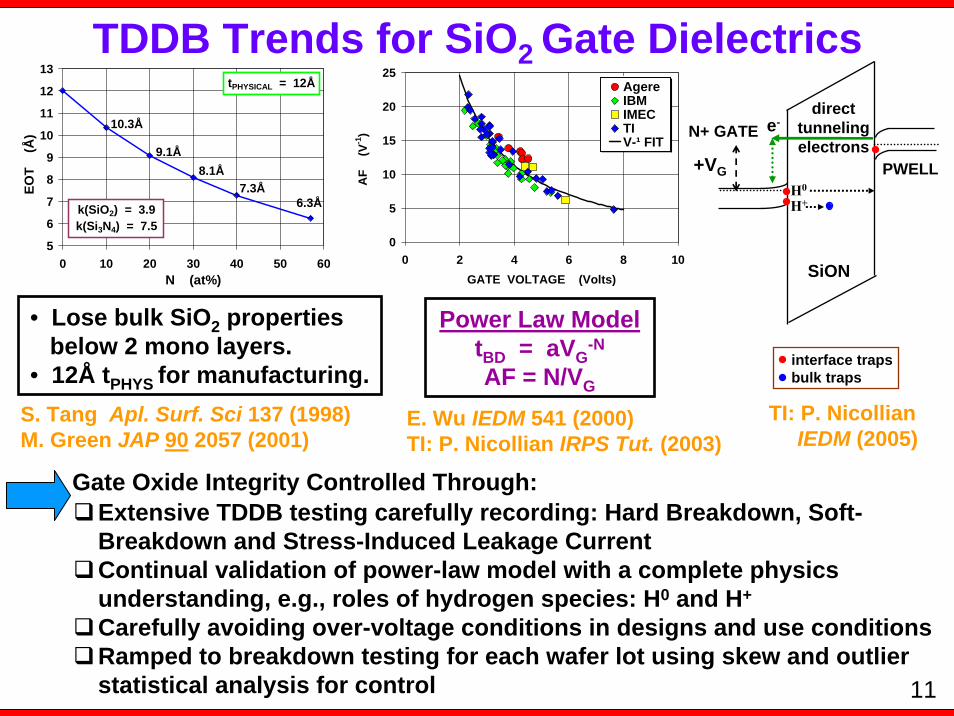
TDDB Trends for SiO2 Gate Dielectrics
TI: P. Nicollian IEDM (2005)
Extensive TDDB testing carefully recording: Hard Breakdown, Soft-Breakdown and Stress-Induced Leakage CurrentContinual validation of power-law model with a complete physics understanding, e.g., roles of hydrogen species: H0 and H+
Carefully avoiding over-voltage conditions in designs and use conditionsRamped to breakdown testing for each wafer lot using skew and outlier statistical analysis for control
Power Law ModeltBD = aVG
-N
AF = N/VG
10.3Å
6.3Å7.3Å
8.1Å9.1Å
5
6
7
8
9
10
11
12
13
0 10 20 30 40 50 60N (at%)
EOT
(Å
)
k(SiO2) = 3.9k(Si3N4) = 7.5
tPHYSICAL = 12Å
• Lose bulk SiO2 properties below 2 mono layers.
• 12Å tPHYS for manufacturing.S. Tang Apl. Surf. Sci 137 (1998)M. Green JAP 90 2057 (2001)
E. Wu IEDM 541 (2000)TI: P. Nicollian IRPS Tut. (2003)
N+ GATE
PWELL
directtunnelingelectrons
SiON
H0
+VG
e-
H+
interface trapsbulk traps
Gate Oxide Integrity Controlled Through:
11
TDDB Trends for High-k Dielectrics
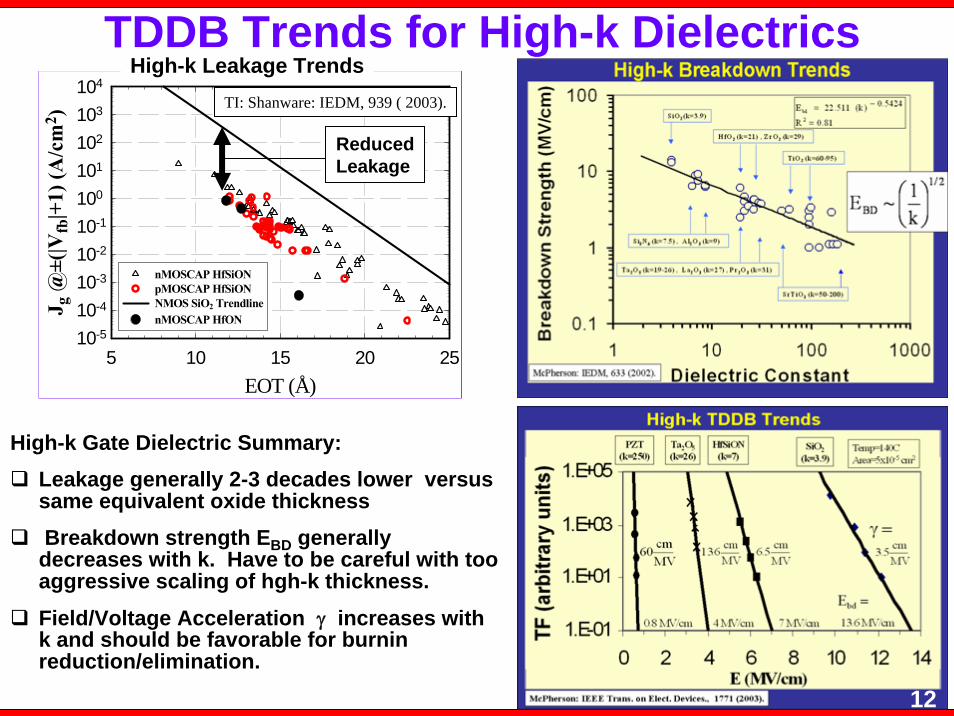
High-k Gate Dielectric Summary: Leakage generally 2-3 decades lower versus same equivalent oxide thicknessBreakdown strength EBD generally decreases with k. Have to be careful with too aggressive scaling of hgh-k thickness.
Field/Voltage Acceleration γ increases with k and should be favorable for burnin reduction/elimination.
EOT (Å)5 10 15 20 25
J g @
±(|V
fb|+
1) (A
/cm
2 )
10-5
10-4
10-3
10-2
10-1
100
101
102
103
104
nMOSCAP HfSiONpMOSCAP HfSiONNMOS SiO2 TrendlinenMOSCAP HfON
TI: Shanware: IEDM, 939 ( 2003).
High-k Leakage Trends
ReducedLeakage
12

NBTI Trends
NBTI Effects Controlled Through:Controlling excessive hydrogenUnderstanding full statistical NBTI-degradation distributionDetermination of critical p-channel speed pathsDesigning with the NBTI-induced shifts comprehendedProduct Margin-Testing/Guard-Banding
-14
-12
-10
-8
-6
-4
-2
0
0.8 0.9 1.0 1.1 1.2 1.3 1.4 1.5
Characterization VDD (V)
ΔF O
SC (%
)Stress1: VDD=2.8V/30mins/105°C
Stress2: VDD=2.8V/60mins/105°C
TI: V. Reddy et. al., IRPS 2002
TI: A. T. Krishnan, IRPS Tutorials 2005
Poly
H HSiO2
Silicon
H0 H0Eox
Interface State Generation Step 1: Si-H(3eV) + hole Si + H+
Step 2: H+ + e H0
Step 3: H0 + H0 H2 (4eV)
13

Channel Hot-Carrier Trends
CHC Effects Controlled Through:Extensive CHC testing --- complete understanding of voltage, temperature and time-dependence of transistor parametric-degradation Determining the full statistical distribution of CHC degradationCircuit checkers, e.g., determination of critical speed pathsDesigning with the CHC-induced parametric shifts fully comprehendedProduct Margin-Testing/Guard-Banding
0.01
0.1
1
10
100
1000
0 50 100 150L (nm)
Life
time
(Arb
itrar
y) NMOSPMOS
Channel Hot Carrier (CHC) Injection can degrade transistor parameters
0.6
0.8
1
1.2
1.4
1.6
0 50 100 150L (nm)
VDD
(V)
Vdd held ~ constant
Vdd reducedwith scaling
Vdd Trends CHC Lifetime Trend
14

0123456789
10
0 20 40 60 80Silicide thickness (nm)
Shee
t res
ista
nce
(ohm
/sq)
CoSi2
NiSi
Silicide Trends
Sheet resistance for NiSi lower than CoSi2For same sheet resistance, average Si consumed is much less with NiSiFor similar junction depth, lower junction leakage achieved with NiSi
32nm Silicide Challenges :Maintaining low sheet-resistance plus low junction-leakage a challengeShallow junctions versus adequate annealing of implant-induced damageRaised source/drains required for low-sheet/low-leakage junctions?
01020304050607080
0 1 2 3 4 5 6 7 8Sheet resistance (ohms/sq)
Silic
on c
onsu
mpt
ion
(nm
)
CoSi2
NiSi
Ref: Lauwers et al, JVST-B, p.2026, 2001
1.E-10
1.E-09
1.E-08
1.E-07
140 145 150 155 160 165 170 175Junction depth (nm)
Leak
age
(A/c
m²)
CoSi2
NiSi
Ref: Lauwers et al, JVST-B, p.2026, 2001
Silicide : NiSi PtSi Pd2SiResistivity: 20-30 25-35 25-35(μohm-cm)
15

Feature Size
IC Process Parameter
Impact on ESD robustness
<1 μm Silicide ↓
<0.25 um Leff ↓Tox <40 A ↓65-90 nm
↓
Poor thermal resistance
Local channel heating
Oxide stress
Metal current density
Ch. Self-heating
Every technology advance has significant impact on ESD design for the IC circuits
32 nmFinFET
SOI
ESD Trends
ESD Controlled Through:Special ESD protection circuits are designed and implemented on chipUnderstanding and mitigating the impact of processing on ESD circuitsESD Checkers are used to aid designers Extensive ESD and Latchup testing of final productJEDIC standards used for shipping, handling and product use
Common Sources for ESD Damage to Semiconductor Devices:
Human Body
Machines
Charged Devices
16

e-
Extrusion
e-
Voids
M
Electromigration-Induced Damage in Metal
TI: E. Ogawa, 2001 IEEE-IRPS Tutorial
Electromigration (EM) Effects Controlled Through:Interconnect Process-RobustnessExtensive EM TestingCurrent Design Rules Based On: Operating Temp, Duty Cycle, AC vs. DC Operation, Metal Length and Width ConsiderationsCurrent Density Checkers and Power-Density (Hot-Spot) Analysis
17
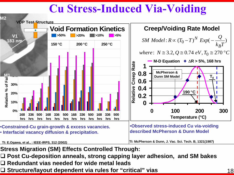
Cu Stress-Induced Via-Voiding
•Constrained-Cu grain-growth & excess vacancies.• Interfacial vacancy diffusion & precipitation.
TI: E.Ogawa, et al., : IEEE-IRPS, 312 (2002)
00.20.40.60.8
1
0 100 200 300
Rel
ativ
e C
reep
Rat
e
Temperature (°C)
M-D Equation ΔR > 5%, 168 hrs
190 °C
T0
CTeVQNwhereTk
QExpTTRModelSMB
N
°≅≅≅
−−∝
270,74.0,2.3:
)()(:
0
0
Creep/Voiding Rate Model
McPherson & Dunn SM Model
•Observed stress-induced Cu via-voiding described McPherson & Dunn Model
VDP Structure Void Formation Kinetics
0%
10%
20%
30%
40%
50%
60%
70%
80%
168 hrs
336hrs
500 hrs
168 hrs
336 hrs
500 hrs
168 hrs
336 hrs
500 hrs
168 hrs
336 hrs
500 hrs
Rel
ativ
e %
of F
ailin
g Si
tes
(48
tota
l)
OPEN >100% >50% >20% >10% >5%
100 °C 150 °C 200 °C 250 °C
VDP Test Structure
M1
M2
183 nmV1
TI: McPherson & Dunn, J. Vac. Sci. Tech. B, 1321(1987)
Stress Migration (SM) Effects Controlled Through:Post Cu-deposition anneals, strong capping layer adhesion, and SM bakesRedundant vias needed for wide metal leads Structure/layout dependent via rules for “critical” vias 18
0 1 2 3 4 5 6 7 8 9 10111210-1100101102103104105106107108109
Tim
e to
Fai
lure
(Arb
itary
Uni
t)
E (MV/cm)
OSG(k=2.9)
FSG(k=3.5)
PETEOS(k=4.2)
SiO2
P-MSQ (k=2.4)
0 1 2 3 4 5 6 7 8 9 10111210-1100101102103104105106107108109
Tim
e to
Fai
lure
(Arb
itary
Uni
t)
E (MV/cm)0 1 2 3 4 5 6 7 8 9 101112
10-1100101102103104105106107108109
Tim
e to
Fai
lure
(Arb
itary
Uni
t)
E (MV/cm)
OSG(k=2.9)
FSG(k=3.5)
PETEOS(k=4.2)
SiO2
P-MSQ (k=2.4)
OSG(k=2.9)
FSG(k=3.5)
PETEOS(k=4.2)
SiO2
P-MSQ (k=2.4)
Lower-k silica-based materials generally have lower Ebd and TDDBLower-k materials generally have lower modulus and lower mechanical strengthUV and/or e-beam shown to be effective at increasing strength/hardness
Low-k Interconnect Dielectric Trends
γ
Low-k Dielectric Issues Controlled Through:Extensive TDDB, adhesion, cohesion, and crack propagation testingDetailed design rules for minimum-pitch line-lengths Dual ramp-rate breakdown testing (TI: G. Haase, et al., IRPS, 466 (2005)
Ebd
TDDB
TI: E. Ogawa, et al., IRPS 2003
19

0
10
20
30
40
50
0 1 2 3 4 5 6Current Density [MA/cm2]
Tem
pera
ture
Ris
e [°
C]
M2, FSG
M3, FSG
M4, FSG
M4, OSG
M3, OSG
M2, OSG
Interconnect Joule Heating Trends Dielectric Thermal Material Constant Conductivity (mW/oC-cm)
PE-TEOS 4.2 ~ 12
FSG 3.6 ~ 8
OSG 2.8 ~ 5
Joule heating in metal leads becomes an issue for current densities > 1MA/cm2 and is exacerbated by low-k. 20

Defect Detection Trends with Scaling
breakdown field (MV/cm)3 4 5 6 7 8 9
cum
ulat
ive
prob
abili
ty %
0.1
1
10
30
50
70
90
99
“Killing Defects” are becoming increasingly difficult to resolve physicallyIn some cases, the killing defect can be atomic/molecular in size. Must rely more on electrical versus physical signature. Electrical breakdown and TDDB measurements of interconnect dielectrics have become standard interconnect reliability test. Dual ramp-rate breakdown tests now used to determine true minimum to metal-to-metal spacing for interconnects hundreds of meters long
0102030405060708090
100
180 130 90 65 45 32
technology nodes (nm)
kille
r de
fect
size
Inm
)
Killing interconnect defects: historically ~ 50% of geometry/space
M1-M1 @250C3hr 1hr
7hr
Actually, today, killing interconnect defects can be atomic/molecular in size
Impact of time-window on ILD breakdown strength
21

Photolithography Issues with Continued Scaling ---What you draw is not exactly
what you get
Information is lost
N3 N4
• Contact pad area loss• Asymmetric pitch CD control
• Constrained gate end loss• Gate CD flaring near pads/turns 22

Lithography – fewer tricks remain
Various Strategies/Tricks:- Attenuated phase shift (130nm)- Model-Based OPC (130nm)- Alternating phase shift (90nm)- Sub-resolution assist feat.( 65nm)- Restricted design rules (45nm)- Immersion lithography (45nm)
32nm Challenges for LithographyHighly restricted design rules and high-index immersion for lithographyDouble-exposure at multiple layersFull 3D-electromagnetic litho simulation for RET/OPC
23
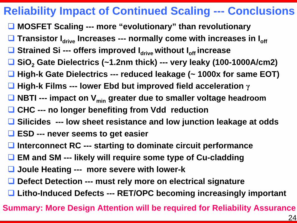
24Summary: More Design Attention will be required for Reliability Assurance
MOSFET Scaling --- more “evolutionary” than revolutionaryTransistor Idrive Increases --- normally come with increases in Ioff
Strained Si --- offers improved Idrive without Ioff increaseSiO2 Gate Dielectrics (~1.2nm thick) --- very leaky (100-1000A/cm2)High-k Gate Dielectrics --- reduced leakage (~ 1000x for same EOT)High-k Films --- lower Ebd but improved field acceleration γNBTI --- impact on Vmin greater due to smaller voltage headroomCHC --- no longer benefiting from Vdd reductionSilicides --- low sheet resistance and low junction leakage at odds ESD --- never seems to get easierInterconnect RC --- starting to dominate circuit performanceEM and SM --- likely will require some type of Cu-claddingJoule Heating --- more severe with lower-k Defect Detection --- must rely more on electrical signatureLitho-Induced Defects --- RET/OPC becoming increasingly important
Reliability Impact of Continued Scaling --- Conclusions


