Recall Constant Envelope Modulation from Lecture 19
Popular for cell phones and cordless phones due to the reduced linearity requirements on the power amp- Allows a more efficient power amp design
Transmitter power is reduced
Baseband to RF Modulation Power Amp
TransmitterOutput
BasebandInput
Constant-Envelope Modulation
TransmitFilter
M.H. Perrott MIT OCW
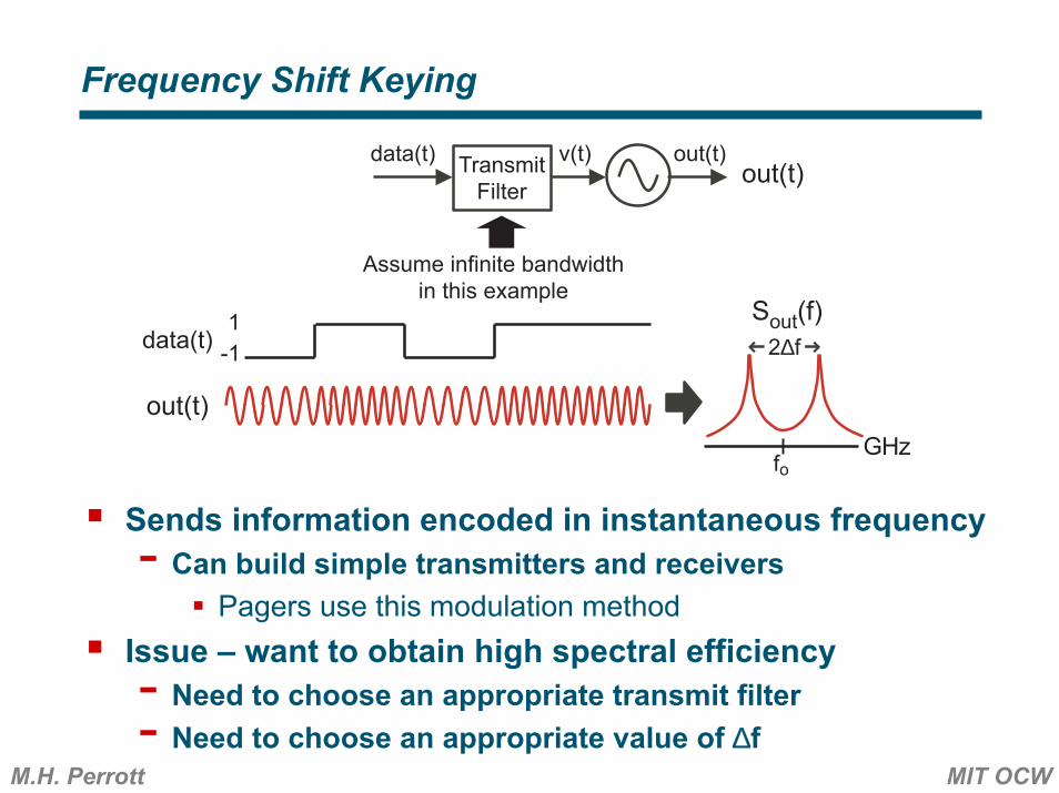
Frequency Shift Keying
Sends information encoded in instantaneous frequency- Can build simple transmitters and receivers
Pagers use this modulation methodIssue – want to obtain high spectral efficiency- Need to choose an appropriate transmit filter- Need to choose an appropriate value of ∆f
GHz
out(t)
out(t)
Sout(f)data(t) 2∆f
TransmitFilter
v(t) out(t)data(t)
Assume infinite bandwidthin this example
fo
1-1
M.H. Perrott MIT OCW
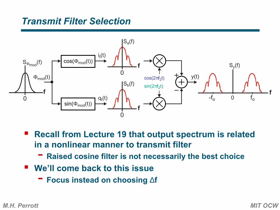
Transmit Filter Selection
Recall from Lecture 19 that output spectrum is related in a nonlinear manner to transmit filter- Raised cosine filter is not necessarily the best choice
We’ll come back to this issue- Focus instead on choosing ∆f
f0
SΦmod(f)
cos(2πf2t)
sin(2πf2t)
y(t)
-fo fo0
cos(Φmod(t))
sin(Φmod(t))
f0
Sa(f)
Sy(f)
it(t)
qt(t)
f0
Sb(f)f
Φmod(t)
M.H. Perrott MIT OCW
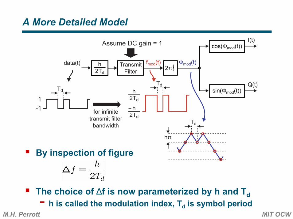
A More Detailed Model
By inspection of figure
The choice of ∆f is now parameterized by h and Td- h is called the modulation index, Td is symbol period
cos(Φmod(t))
sin(Φmod(t))
I(t)
Q(t)
Φmod(t)2πTransmit
Filterfmod(t)data(t) h
Assume DC gain = 1
1-1
2Td
h2Td
h2Td
for infinitetransmit filter
bandwidth
hπ
Td
TdTd
M.H. Perrott MIT OCW
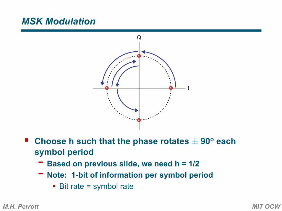
MSK Modulation
Choose h such that the phase rotates ± 90o each symbol period- Based on previous slide, we need h = 1/2- Note: 1-bit of information per symbol period
Bit rate = symbol rate
I
Q
M.H. Perrott MIT OCW
A More Convenient Model for Analysis
Same as previous model, but we represent data as impulses convolved with a rectangular pulse- Note that h = 1/2 for MSK
cos(Φmod(t))
sin(Φmod(t))
I(t)
Q(t)
Φmod(t)2πTransmit
Filterfmod(t)data(t) h
Assume DC gain = 1
2Td
h2Td
h2Td
for infinitetransmit filter
bandwidth
hπ
Td
TdTd
1
-1
Td
01x(t)
M.H. Perrott MIT OCW
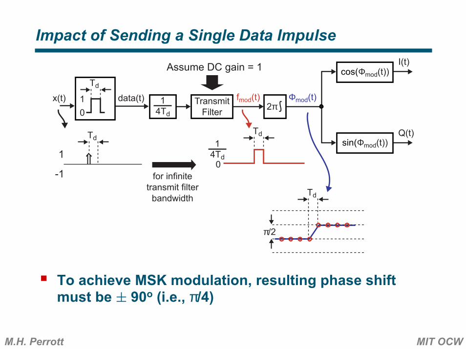
Impact of Sending a Single Data Impulse
To achieve MSK modulation, resulting phase shift must be ± 90o (i.e., π/4)
cos(Φmod(t))
sin(Φmod(t))
I(t)
Q(t)
Φmod(t)2πTransmit
Filterfmod(t)data(t) 1
Assume DC gain = 1
4Td
14Td
for infinitetransmit filter
bandwidth
π/2
Td
TdTd
1
-1
Td
01x(t)
0
M.H. Perrott MIT OCW
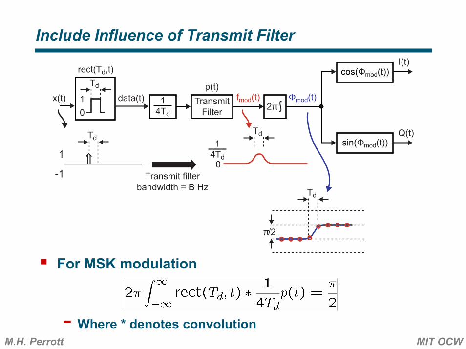
Include Influence of Transmit Filter
For MSK modulation
- Where * denotes convolution
cos(Φmod(t))
sin(Φmod(t))
I(t)
Q(t)
Φmod(t)2πTransmit
Filterfmod(t)data(t) 1
4Td
14Td
Transmit filterbandwidth = B Hz
π/2
Td
TdTd
1
-1
Td
01x(t)
0
rect(Td,t)
p(t)
M.H. Perrott MIT OCW
Gaussian Minimum Shift Keying
Definition- Minimum shift keying in which the transmit filter is chosen
to have a Gaussian shape (in time and frequency) with bandwidth = B Hz
Key parameters- Modulation index: as previously discussed
h = 1/2- BTd product: ratio of transmit filter bandwidth to data rate
For GSM phones: BTd = 0.3
M.H. Perrott MIT OCW
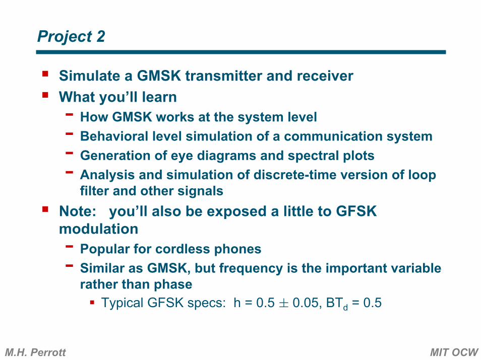
Project 2
Simulate a GMSK transmitter and receiverWhat you’ll learn- How GMSK works at the system level- Behavioral level simulation of a communication system- Generation of eye diagrams and spectral plots- Analysis and simulation of discrete-time version of loop
filter and other signalsNote: you’ll also be exposed a little to GFSK modulation- Popular for cordless phones- Similar as GMSK, but frequency is the important variable
rather than phaseTypical GFSK specs: h = 0.5 ± 0.05, BTd = 0.5
M.H. Perrott MIT OCW
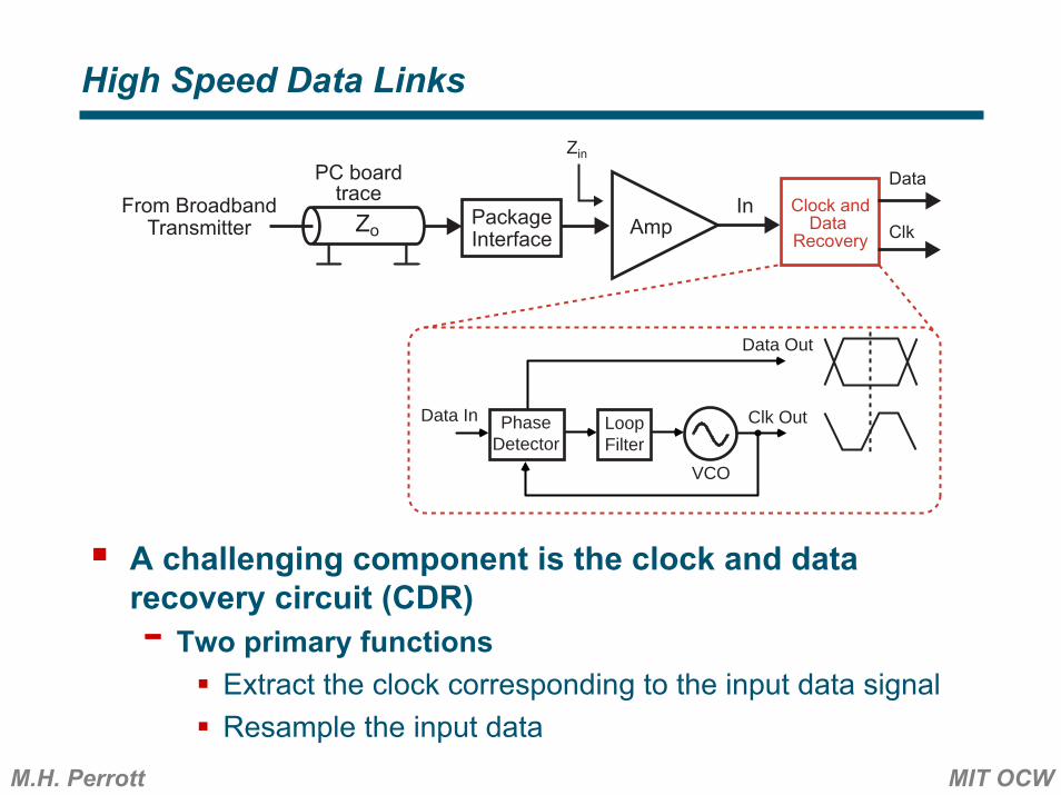
High Speed Data Links
A challenging component is the clock and data recovery circuit (CDR)- Two primary functions
Extract the clock corresponding to the input data signalResample the input data
Zin
Zo AmpFrom Broadband
Transmitter
PC boardtrace
PackageInterface
In Clock andData
Recovery
Data
Clk
LoopFilter
PhaseDetector
Data Out
Data In Clk Out
VCO
M.H. Perrott MIT OCW
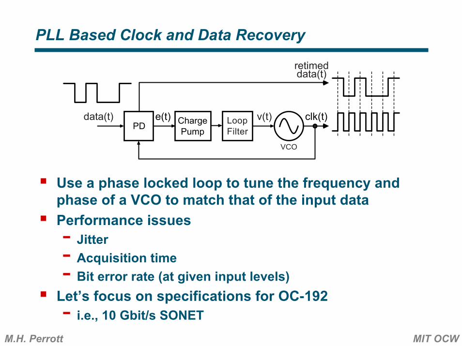
PLL Based Clock and Data Recovery
Use a phase locked loop to tune the frequency and phase of a VCO to match that of the input dataPerformance issues- Jitter- Acquisition time- Bit error rate (at given input levels)
Let’s focus on specifications for OC-192- i.e., 10 Gbit/s SONET
PD ChargePump
clk(t)e(t) v(t)LoopFilter
VCO
retimeddata(t)
data(t)
M.H. Perrott MIT OCW
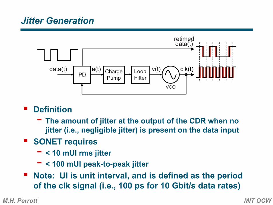
Jitter Generation
Definition- The amount of jitter at the output of the CDR when no
jitter (i.e., negligible jitter) is present on the data inputSONET requires- < 10 mUI rms jitter- < 100 mUI peak-to-peak jitter
Note: UI is unit interval, and is defined as the period of the clk signal (i.e., 100 ps for 10 Gbit/s data rates)
PD ChargePump
clk(t)e(t) v(t)LoopFilter
VCO
retimeddata(t)
data(t)
M.H. Perrott MIT OCW
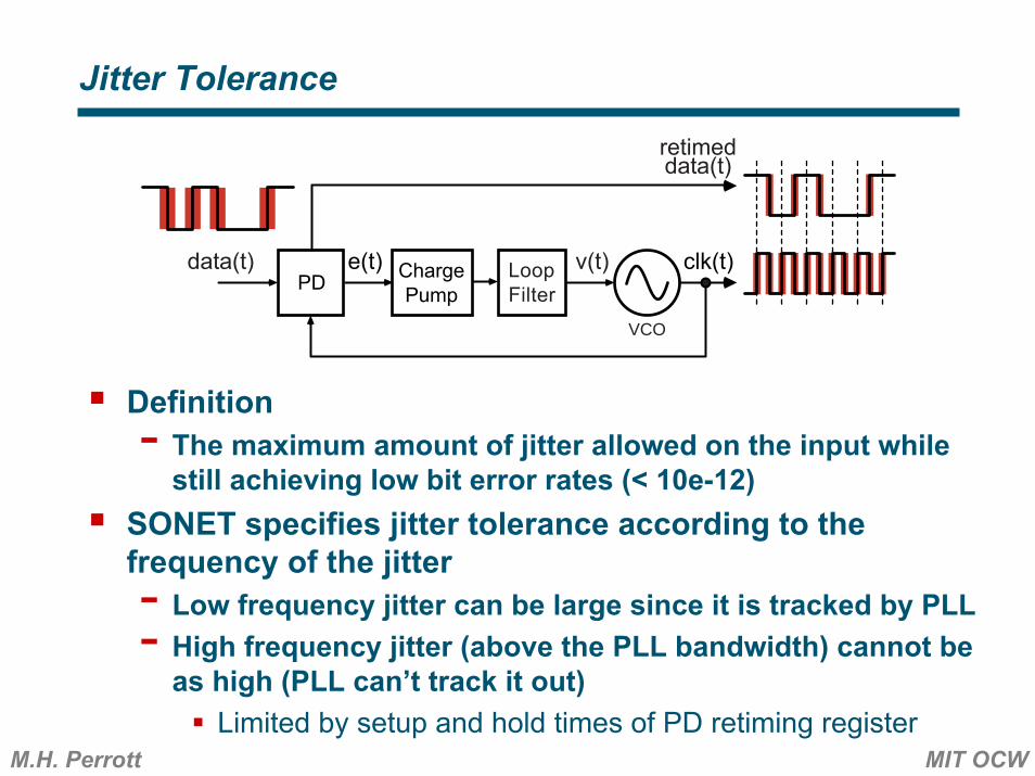
Jitter Tolerance
Definition- The maximum amount of jitter allowed on the input while
still achieving low bit error rates (< 10e-12)SONET specifies jitter tolerance according to the frequency of the jitter- Low frequency jitter can be large since it is tracked by PLL- High frequency jitter (above the PLL bandwidth) cannot be
as high (PLL can’t track it out)Limited by setup and hold times of PD retiming register
PD ChargePump
clk(t)e(t) v(t)LoopFilter
VCO
retimeddata(t)
data(t)
M.H. Perrott MIT OCW
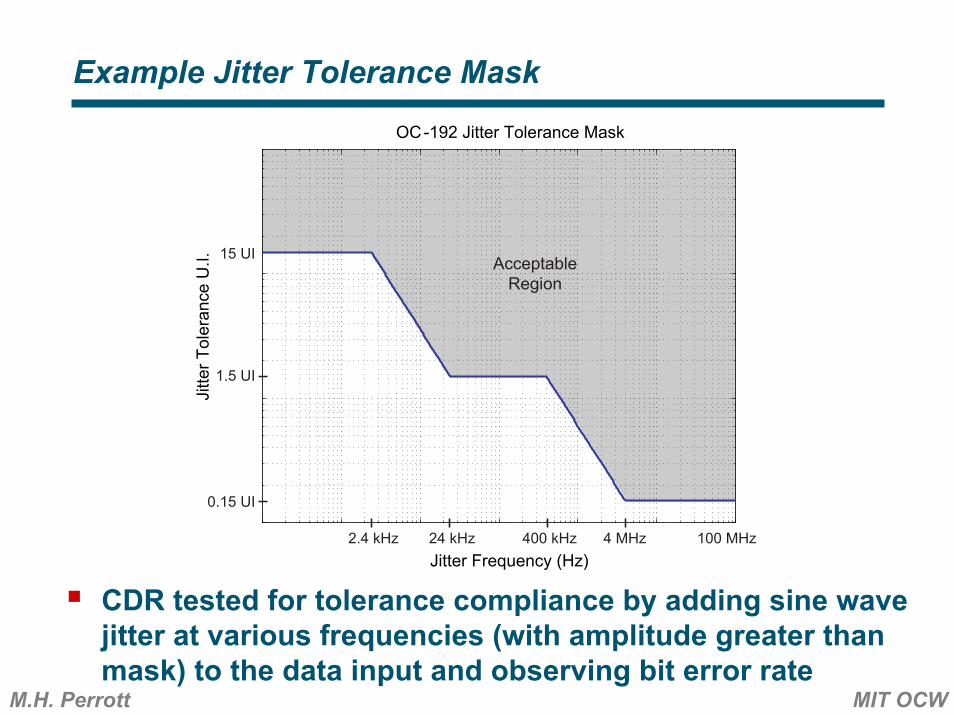
Example Jitter Tolerance Mask
CDR tested for tolerance compliance by adding sine wave jitter at various frequencies (with amplitude greater than mask) to the data input and observing bit error rate
Jitter Frequency (Hz)
Jitte
r Tol
eran
ce U
.I.
OC-192 Jitter Tolerance Mask
24 kHz 4 MHz 100 MHz
0.15 UI
1.5 UI
15 UI
400 kHz2.4 kHz
AcceptableRegion
M.H. Perrott MIT OCW
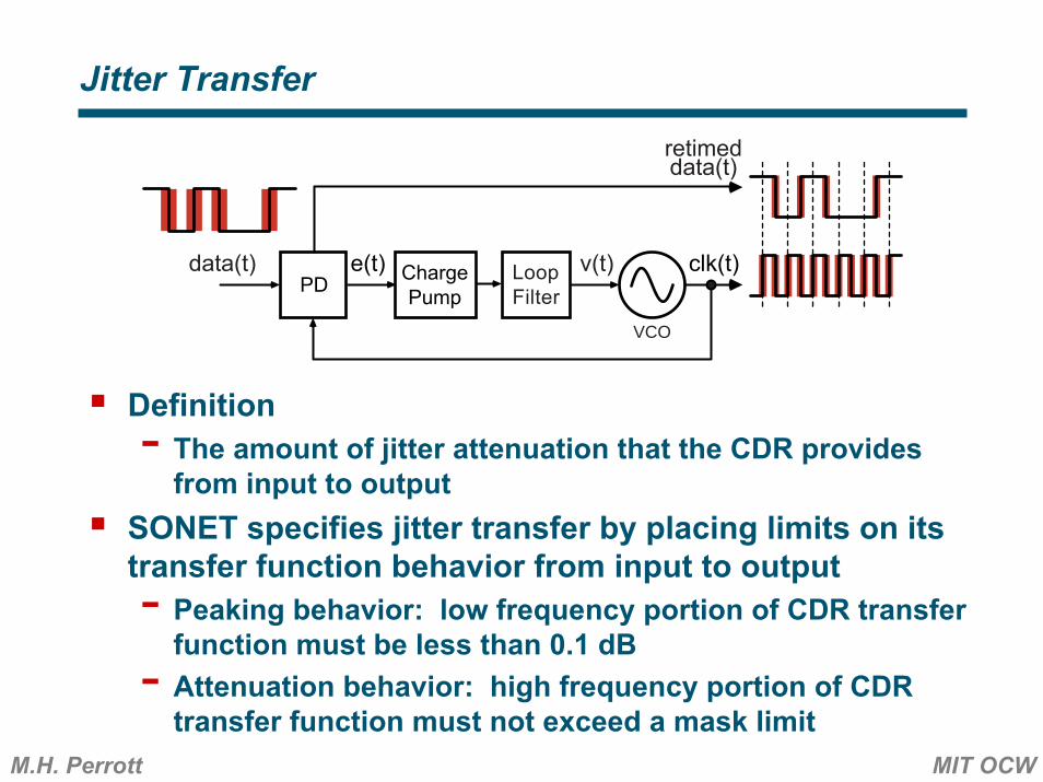
Jitter Transfer
Definition- The amount of jitter attenuation that the CDR provides
from input to outputSONET specifies jitter transfer by placing limits on its transfer function behavior from input to output- Peaking behavior: low frequency portion of CDR transfer
function must be less than 0.1 dB- Attenuation behavior: high frequency portion of CDR
transfer function must not exceed a mask limit
PD ChargePump
clk(t)e(t) v(t)LoopFilter
VCO
retimeddata(t)
data(t)
M.H. Perrott MIT OCW
Example Jitter Transfer Mask
CDR tested for compliance by adding sine wave jitter at various frequencies and observing the resulting jitter at the CDR output
-35
-30
-25
-20
-15
-10
-5
0.1
Frequency (Hz)
Mag
nitu
de (d
B)
100 kHz 8 MHz 100 MHz1 MHz10 kHz
AcceptableRegion
OC-192 Jitter Transfer Mask
Maximum Allowed "Peaking" = 0.1 dB
M.H. Perrott MIT OCW
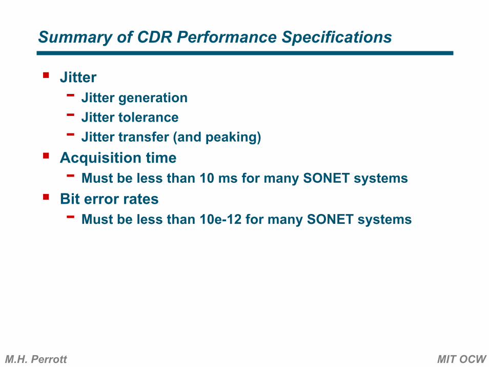
Summary of CDR Performance Specifications
Jitter- Jitter generation- Jitter tolerance- Jitter transfer (and peaking)
Acquisition time- Must be less than 10 ms for many SONET systems
Bit error rates- Must be less than 10e-12 for many SONET systems
M.H. Perrott MIT OCW
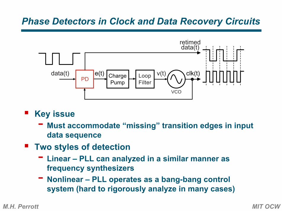
Phase Detectors in Clock and Data Recovery Circuits
Key issue- Must accommodate “missing” transition edges in input
data sequenceTwo styles of detection- Linear – PLL can analyzed in a similar manner as
frequency synthesizers- Nonlinear – PLL operates as a bang-bang control
system (hard to rigorously analyze in many cases)
PD ChargePump
clk(t)e(t) v(t)LoopFilter
VCO
retimeddata(t)
data(t)
M.H. Perrott MIT OCW
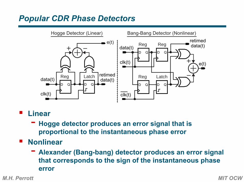
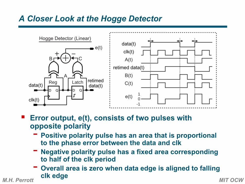
Popular CDR Phase Detectors
Linear- Hogge detector produces an error signal that is
proportional to the instantaneous phase errorNonlinear- Alexander (Bang-bang) detector produces an error signal
that corresponds to the sign of the instantaneous phase error
Error output, e(t), consists of two pulses with opposite polarity- Positive polarity pulse has an area that is proportional
to the phase error between the data and clk- Negative polarity pulse has a fixed area corresponding to half of the clk period- Overall area is zero when data edge is aligned to falling clk edge
clk(t)data(t)
retimed data(t)
e(t)
A
A(t)B
B(t)
C
C(t)
1
-10
D Q D Q
clk(t)
data(t)retimeddata(t)
Reg Latch
e(t)
Hogge Detector (Linear)
M.H. Perrott MIT OCW
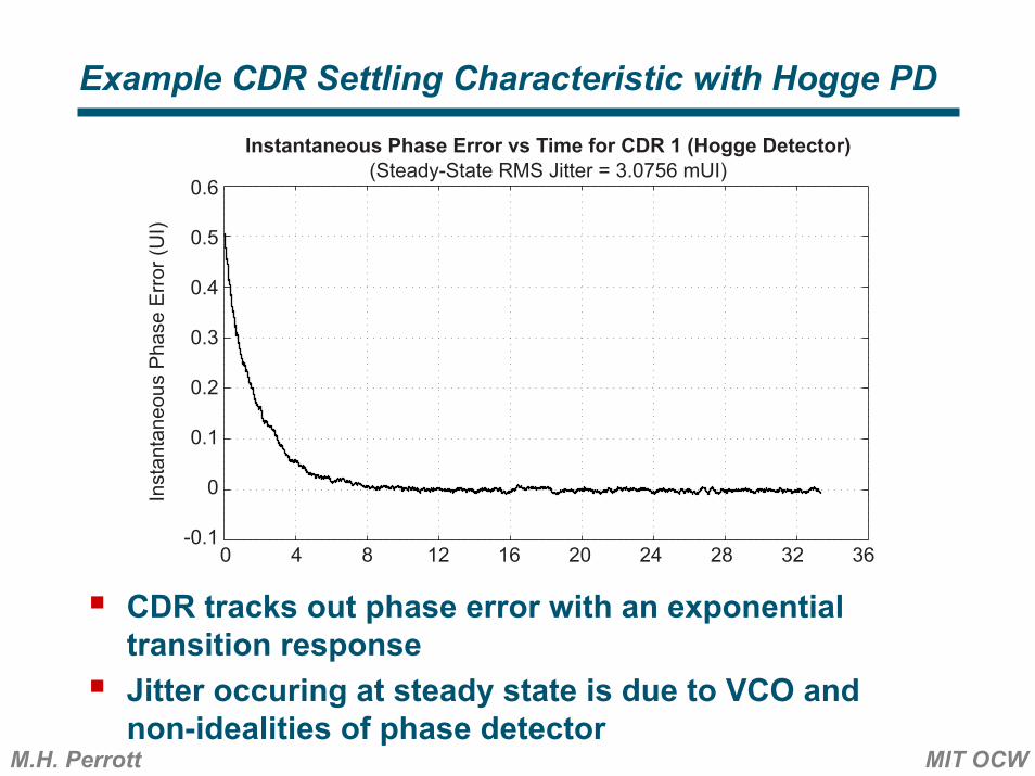
Example CDR Settling Characteristic with Hogge PD
CDR tracks out phase error with an exponential transition responseJitter occuring at steady state is due to VCO and non-idealities of phase detector
Inst
anta
neou
s Ph
ase
Erro
r (U
I)0.6
0.5
0.4
0.3
0.2
0.1
0
36322824201612840-0.1
Instantaneous Phase Error vs Time for CDR 1 (Hogge Detector)(Steady-State RMS Jitter = 3.0756 mUI)
M.H. Perrott MIT OCW
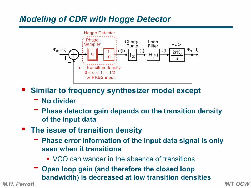
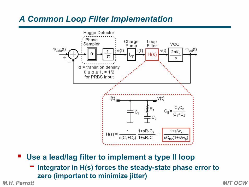
Modeling of CDR with Hogge Detector
Similar to frequency synthesizer model except- No divider- Phase detector gain depends on the transition density
of the input dataThe issue of transition density- Phase error information of the input data signal is only
seen when it transitionsVCO can wander in the absence of transitions
- Open loop gain (and therefore the closed loop bandwidth) is decreased at low transition densities
Key issue: an undesired pole/zero pair occurs due to stabilizing zero in the lead/lag filter
Non-dominantpole
Dominantpole pair
Open loopgain
increased
120o
-180o
-140o
-160o
20log|A(f)|
ffz
0 dB
PM = 55o for CPM = 53o for APM = 54o for B
angle(A(f))
A
A
A
A
B
B
B
B
C
C
C
C
Evaluation ofPhase Margin
Closed Loop PoleLocations of G(f)
fp
Re{s}
Im{s}
0
M.H. Perrott MIT OCW
Corresponding Closed Loop Frequency Response
Undesired pole/zero pair causes peaking in the closed loop frequency responseSONET demands that peaking must be less than 0.1 dB- For classical lead/lag filter approach, this must be achieved
by having a very low-valued zeroRequires a large loop filter capacitor
wwowz
wzwcp
|G(w)| Peaking caused byundesired pole/zero pair
0
1
Frequency (rad/s)
M.H. Perrott MIT OCW
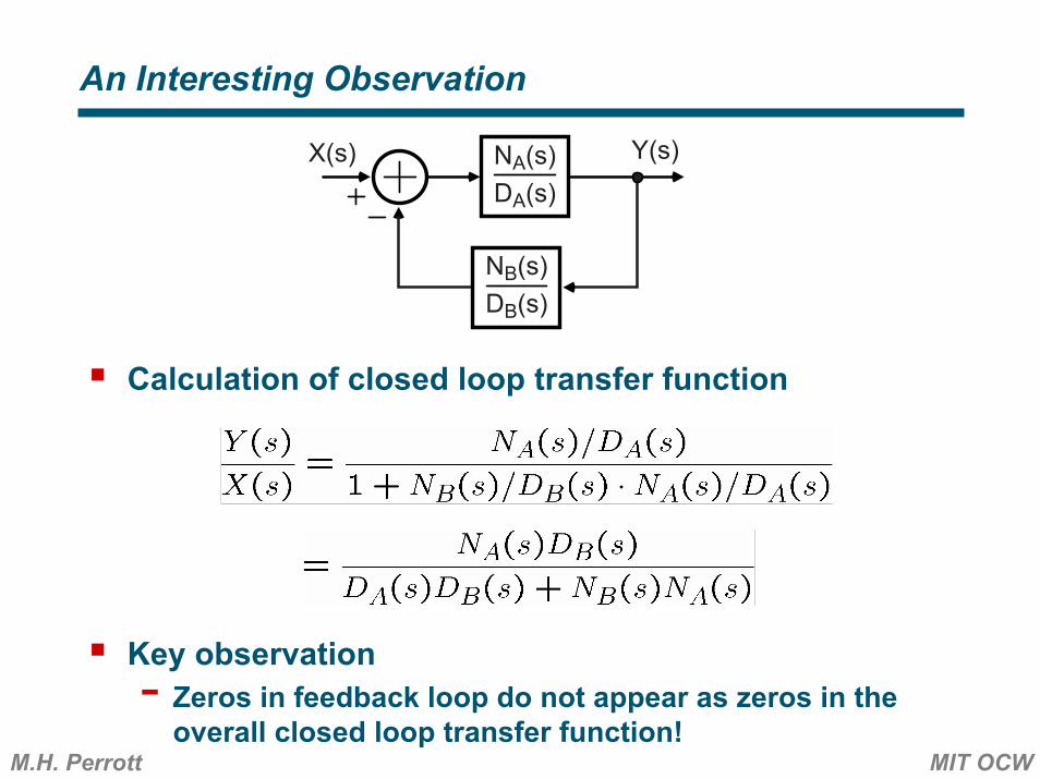
An Interesting Observation
Calculation of closed loop transfer function
Key observation- Zeros in feedback loop do not appear as zeros in the
overall closed loop transfer function!
NA(s)X(s)DA(s)
Y(s)
NB(s)DB(s)
M.H. Perrott MIT OCW
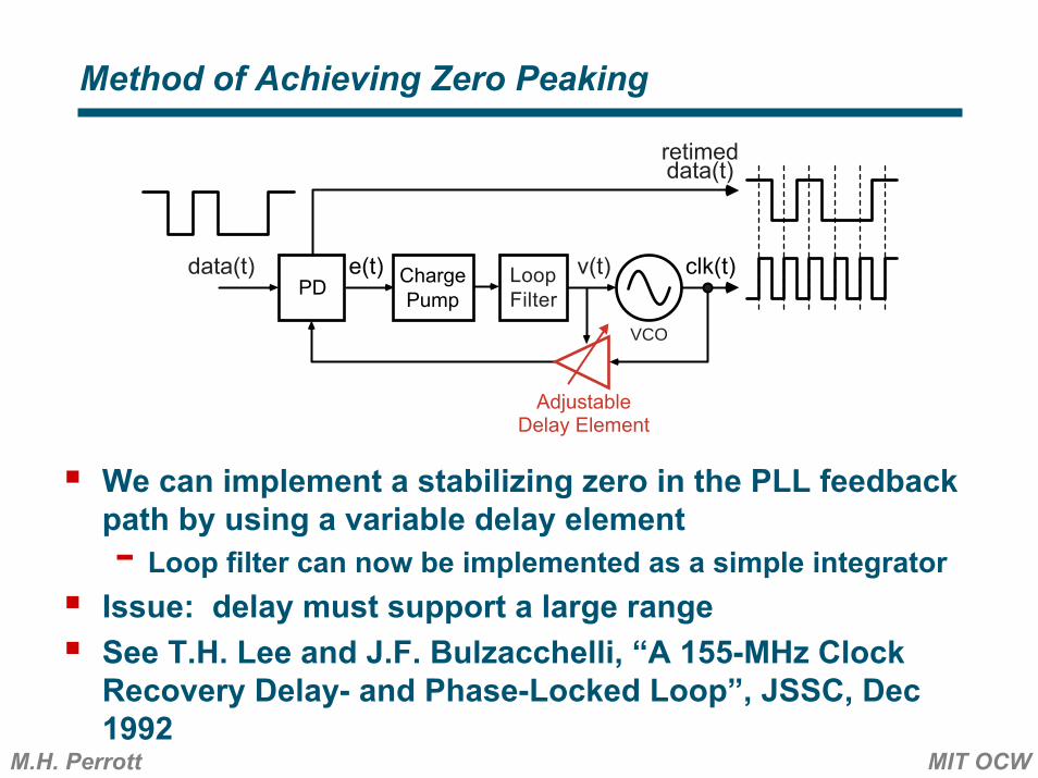
Method of Achieving Zero Peaking
We can implement a stabilizing zero in the PLL feedback path by using a variable delay element- Loop filter can now be implemented as a simple integrator
Issue: delay must support a large rangeSee T.H. Lee and J.F. Bulzacchelli, “A 155-MHz Clock Recovery Delay- and Phase-Locked Loop”, JSSC, Dec 1992
PD ChargePump
clk(t)e(t) v(t)LoopFilter
VCO
retimeddata(t)
data(t)
AdjustableDelay Element
M.H. Perrott MIT OCW
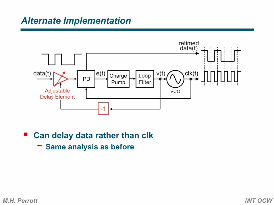
Model of CDR with Delay Element
Delay “gain”, Kd, is set by delay implementationNote that H(s) can be implemented as a simple capacitor- H(s) = 1/(sC)
Can delay data rather than clk- Same analysis as before
PD ChargePump
clk(t)e(t) v(t)LoopFilter
VCO
retimeddata(t)
data(t)
-1
AdjustableDelay Element
M.H. Perrott MIT OCW
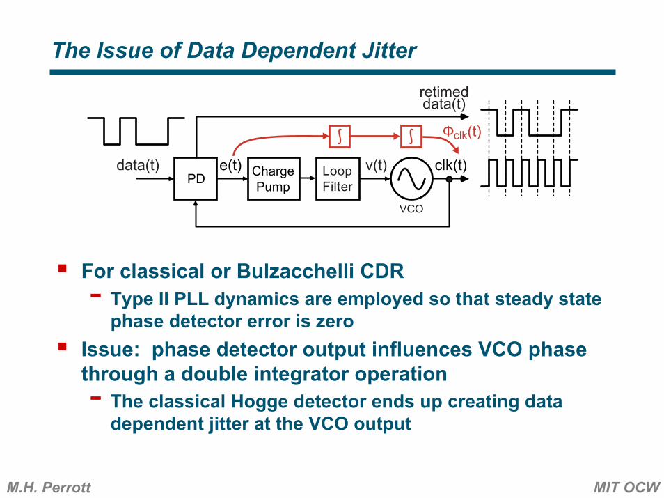
The Issue of Data Dependent Jitter
For classical or Bulzacchelli CDR- Type II PLL dynamics are employed so that steady state
phase detector error is zeroIssue: phase detector output influences VCO phase through a double integrator operation- The classical Hogge detector ends up creating data
dependent jitter at the VCO output
PD ChargePump
clk(t)e(t) v(t)LoopFilter
VCO
retimeddata(t)
data(t)
Φclk(t)
M.H. Perrott MIT OCW
Culprit Behind Data Dependent Jitter for Hogge PD
The double integral of the e(t) pulse sequence is nonzero (i.e., has DC content)- Since the data transition activity is random, a low
frequency noise source is createdLow frequency noise not attenuated by PLL dynamics
A
B C
D Q D Q
clk(t)
data(t)retimeddata(t)
Reg Latch
e(t)
clk(t)
data(t)
retimed data(t)
e(t)
A(t)
B(t)C(t)
1
-10
Hogge Detector (Linear)
e(t) 0
M.H. Perrott MIT OCW
One Possible Fix
Modify Hogge so that the double integral of the e(t) pulse sequence is zero- Low frequency noise is now removed
See L. Devito et. al., “A 52 MHz and 155 MHz Clock-recovery PLL”, ISSCC, Feb, 1991
clk(t)
data(t)
retimed data(t)
e(t)
A
A(t)
B B(t)CC(t)
1
-2
0
clk(t)
data(t)retimeddata(t)
D Q
Reg
e(t)
D Q
Latch
Hogge Detector (Linear)
D(t)
e(t) 0
Latch
D Q
D2
M.H. Perrott MIT OCW
A Closer Look at the Bang-Bang Detector
Error output consists of pulses of fixed area that are either positive or negative depending on phase errorPulses occur at data edges- Data edges detected when sampled data sequence is
different than its previous valueAbove example illustrates the impact of having the data edge lagging the clock edge
clk(t)data(t)
retimed data(t)
e(t)
A(t)
B(t)
C(t)
1
-10
D Q D Q
Reg Latch
D Q D Q
clk(t) e(t)
data(t)retimeddata(t)Reg Reg
clk(t)
Bang-Bang Detector (Nonlinear)
A
B
C
D D(t)
M.H. Perrott MIT OCW
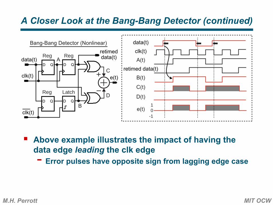
A Closer Look at the Bang-Bang Detector (continued)
Above example illustrates the impact of having the data edge leading the clk edge- Error pulses have opposite sign from lagging edge case
clk(t)data(t)
retimed data(t)
e(t)
A(t)
B(t)
C(t)
1
-10
D Q D Q
Reg Latch
D Q D Q
clk(t) e(t)
data(t)retimeddata(t)Reg Reg
clk(t)
Bang-Bang Detector (Nonlinear)
A
B
C
D D(t)
M.H. Perrott MIT OCW
Example CDR Settling Characteristic with Bang-Bang PD
Bang-bang CDR response is slew rate limited- Much faster than linear CDR, in generalSteady-state jitter often dominated by bang-bang behavior (jitter set by error step size and limit cycles)
Inst
anta
neou
s Ph
ase
Erro
r (U
I)0.05
0
-0.05
-0.1
-0.15
-0.220181614121086420
Time (Micro Seconds)
Instantaneous Phase Error vs Time for CDR 2 (Bang-Bang Detector)(Steady-State RMS Jitter = 3.4598 mUI)
M.H. Perrott MIT OCW
The Issue of Limit Cycles
Bang-bang loops exhibit limit cycles during steady-state operation- Above diagram shows resulting waveforms when data
transitions on every cycle- Signal patterns more complicated for data that randomly
transitionsFor lowest jitter: want to minimize period of limit cycles
clk(t)e(t) v(t)
VCO
data(t)Sense Drive
Φclk(t)Bang-Bang Style Phase Detector
Φclk(t)
e(t)
v(t)
M.H. Perrott MIT OCW
The Impact of Delays in a Bang-Bang Loop
Delays increase the period of limit cycles, thereby increasing jitter
clk(t)e(t) v(t)
VCO
data(t)Sense DriveDelay
Φclk(t)Bang-Bang Style Phase Detector
Φclk(t)
e(t)
v(t)
Φclk(t)
e(t)
v(t)
M.H. Perrott MIT OCW
Practical Implementation Issues for Bang-Bang Loops
Minimize limit cycle periods- Use phase detector with minimal delay to error output- Implement a high bandwidth feedforward path in loop
filterOne possibility is to realize feedforward path in VCO
See B. Lai and R.C Walker, “A Monolithic 622 Mb/s Clock Extraction Data Retiming Circuit”, ISSCC, Feb 1991
Avoid dead zones in phase detector- Cause VCO phase to wonder within the dead zone,
thereby increasing jitterUse simulation to examine system behavior- Nonlinear dynamics can be non-intuitive- For first order analysis, see R.C. Walter et. al., “A Two-
Chip 1.5-GBd Serial Link Interface”, JSSC, Dec 1992
M.H. Perrott MIT OCW
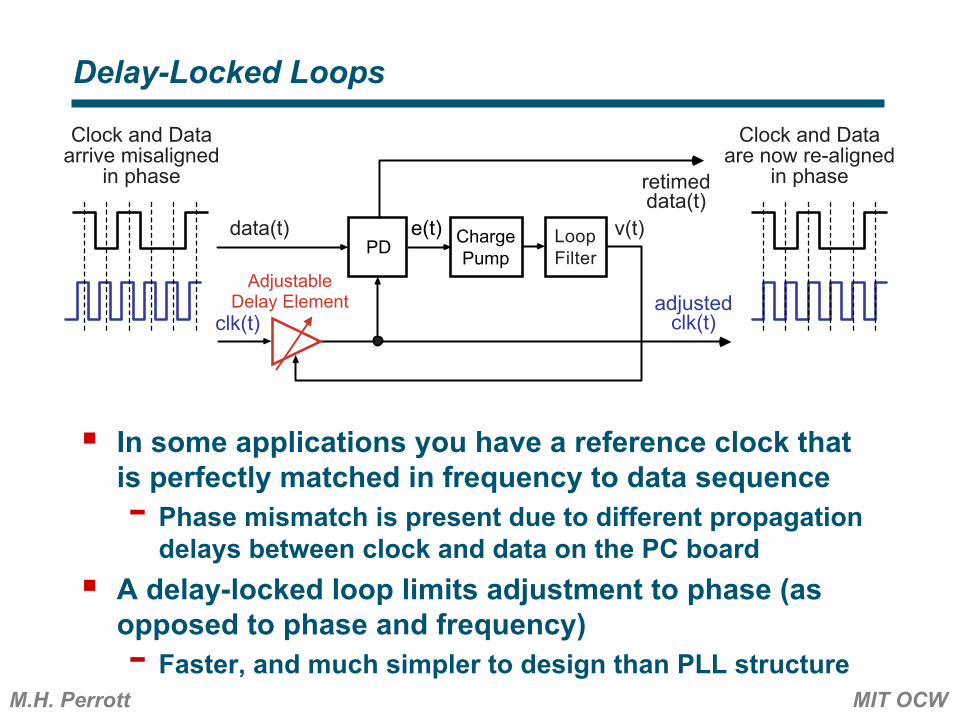
Delay-Locked Loops
In some applications you have a reference clock that is perfectly matched in frequency to data sequence- Phase mismatch is present due to different propagation
delays between clock and data on the PC boardA delay-locked loop limits adjustment to phase (as opposed to phase and frequency)- Faster, and much simpler to design than PLL structure
PD ChargePump
e(t) v(t)LoopFilter
retimeddata(t)
data(t)
AdjustableDelay Element
clk(t)
Clock and Dataarrive misaligned
in phase
Clock and Dataare now re-aligned
in phase
adjustedclk(t)
M.H. Perrott MIT OCW
Some References on CDR’s and Delay-Locked Loops
Gu-Yeon Wei will discuss DLL’s in his guest lectureTom Lee has a nice paper- See T. Lee et. al., “A 2.5 V CMOS Delay-Locked Loop for an
18 Mbit, 500 Megabyte/s DRAM”, JSSC, Dec 1994Check out papers from Mark Horowitz’s group at Stanford- Oversampling data recovery approach
See C-K K. Yang et. al., “A 0.5-um CMOS 4.0-Gbit/s Serial Link Transceiver with Data Recovery using Oversampling”, JSSC, May 1998
- Multi-level signalingSee Ramin Farjad-Rad et. al., “A 0.3-um CMOS 8-Gb/s 4-PAM Serial Link Transceiver”, JSSC, May 2000
- Bi-directional signalingSee E. Yeung, “A 2.4 Gb/s/pin simultaneous bidirectional