28
WELCOME
| Date post: | 02-Aug-2015 |
| Category: |
Engineering |
| Upload: | grace-abraham |
| View: | 104 times |
| Download: | 3 times |

WELCOME

A 128 Kbit SRAM WITH AN EMBEDDED ENERGY MONITORING CIRCUIT AND SENSE-AMPLIFIER OFFSET COMPENSATION USING BODY BIASING
GRACE ABRAHAM ROLL . NO : 01 S1 MTECH VLSI & ES FISAT
Dept. of ECE 206/01/2015

CONTENTS• INTRODUCTION
• MEMORY WITH ASSISTS FOR LOW VOLTAGE OPERATION
• SENSING SCHEME
• TWO STAGE SENSING
• BBSA DESIGN
• ENERGY-MONITORING CIRCUIT FOR SRAM
• MEASUREMENT RESULTS
• CONCLUSION
Dept. of ECE 3
A 128 Kbit SRAM With An Embedded Energy Monitoring Circuit
06/01/2015

INTRODUCTION• Integrating more functionality on a single chip
• SRAMs
• Proposing An embedded energy monitoring circuit
o Limit performance o Energy consumptiono Areao Access time
Dept. of ECE 4
Systems are more complex Work optimally under dynamic conditions
Fundamental building block of complex systems Critical component
Low power operation Better integration system Low operating voltages
A 128 Kbit SRAM With An Embedded Energy Monitoring Circuit
06/01/2015

• 8T –bit cells with write assist are used
• SRAM performance is improved by
• This seminar includes
Dept. of ECE 5
Measures absolute energy consumption of 128 Kbit SRAM 65nm low – power CMOS process
To achieve a wide voltage range of SRAM operation
An offset compensated sense amplifier 2-stage sensing scheme
Low-voltage operation technique Sensing scheme Design and challenges of energy monitoring circuit Test chip measurements
A 128 Kbit SRAM With An Embedded Energy Monitoring Circuit
06/01/2015

MEMORY WITH ASSISTS FOR LOW VOLTAGE OPERATION
Dept. of ECE 6
• Basic building block of SRAM : 6T bit-cell
• 8T bit-cell is used Voltage stability problem
Write operation : WWL , BL , BLB ports Read operation by read buffer : RWL , RBL ports Not compatible with column interleaving
A 128 Kbit SRAM With An Embedded Energy Monitoring Circuit
Fig 1 : 6T SRAM Cell
06/01/2015

Dept. of ECE 7
DCVSL type level converters (LC) are used To address a write assist scheme we utilize an increased supply voltage for VwwL Read buffer transistors
A 128 Kbit SRAM With An Embedded Energy Monitoring Circuit
Fig 2 : 8T bit cell based design with write assist enable operation down to 0.37 V
06/01/2015
Dept. of ECE 8
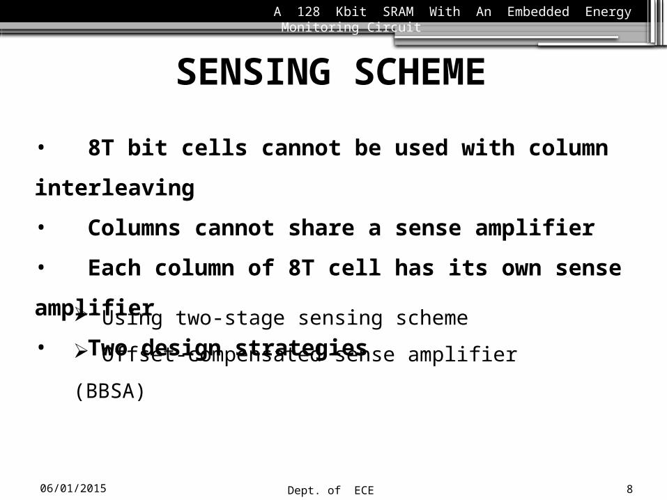
SENSING SCHEME
• 8T bit cells cannot be used with column interleaving
• Columns cannot share a sense amplifier
• Each column of 8T cell has its own sense amplifier
• Two design strategies
Using two-stage sensing scheme
Offset-compensated sense amplifier (BBSA)
A 128 Kbit SRAM With An Embedded Energy Monitoring Circuit
06/01/2015

TWO STAGE SENSING
• SRAMS employ small signal sensing scheme
A 128 Kbit SRAM With An Embedded Energy Monitoring Circuit
Dept. of ECE 9
Fig 3 : Organization of our 128 kbit SRAM
06/01/2015

Dept. of ECE 10
First level sensing (FLS)
Second level sensing (SLS)
o 2 inverters and a PMOS transistors
FBL are precharged to VDD by “pcghb” signal SBL are discharged to 0 Reading starts with RWL signal If data stored is “0”, FBL is at high If data stored is “1”, FBL starts to discharge
o BBSA
Short first level bit lines (FBL) Long second level bit lines (SBL)
• Long bit lines are replaced by
• Signal developed on bit lines are sensed in 2 stages
• Read operation
Signal on FBL transferred to SBL by FLS circuit If FBL is discharged
o PMOS in FLS is ON & starts to charge up SBL
A 128 Kbit SRAM With An Embedded Energy Monitoring Circuit
06/01/2015

Dept. of ECE 11
Signal on SBL is sensed by BBSA
• Signals during 2 read operations
1st clock cycle : read data ‘0’
2nd clock cycle : read data ‘1’
o FBL , SBL stays at their precharged values
o FBL discharges to 0 & is transferred to SBLo SBL starts to charge up
A 128 Kbit SRAM With An Embedded Energy Monitoring Circuit
Fig 4 : Two stage sensing signals during 2 read cycles
06/01/2015

Dept. of ECE 12
• FLS
• SLS
• DO flip depends on the sense enable (snsEn) signal
• Energy consumption is data dependent
• FLS inverters have shifted VTC
• Maximize the ratio of read access
time improvement to the FLS area
overhead
2 static inverters For large level sensing
For small signal sensing
100mV shift maximizes the ratio
A 128 Kbit SRAM With An Embedded Energy Monitoring Circuit
Fig 5 : 100mV VTC shift is used for the FLS inverters
06/01/2015

BBSA DESIGN
Dept. of ECE 13
• Sense Amplifier
• Pseudo-differential sensing
• To decrease sense amplifier offset
• Offset voltage : either +ve or -ve
To sense low power signals from a bit line which represents a data bit Amplify small voltage swing to recognizable logic levels Sense small signal input differences Limited by its input –referred offset For large level sensing
SBL , REF are inputs
Increasing area
Determined during calibration process
A 128 Kbit SRAM With An Embedded Energy Monitoring Circuit
06/01/2015

Dept. of ECE 14
• BBSA utilized body-biasing By controlling VP1 & VP2 of M2 & M3 M16 to M19 are PMOS transistors that drive VP1 &VP2 to VDD=1.2V, VDDB=1.35V VDDB is second voltage source
A 128 Kbit SRAM With An Embedded Energy Monitoring Circuit
Fig 6 : Body-biased amplifier (BBSA)
06/01/2015
Dept. of ECE 15
Fig. 3.2. Segmentation of a seven-gesture sequence in the order up-down-left-right-tick-circle-cross.Fig. 3.2. Segmentation of a seven-gesture sequence in the order up-down-left-right-tick-circle-cross.Fig. 3.2. Segmentation of a seven-gesture sequence in the order up-down-left-right-tick-circle-cross.
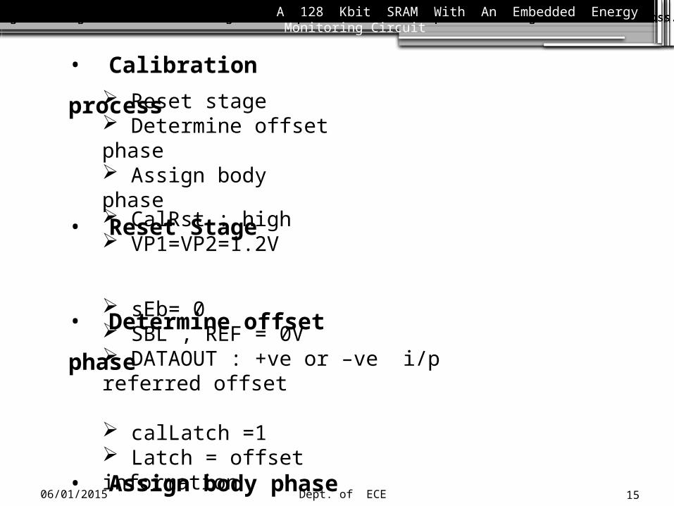
• Calibration process
• Reset Stage
• Determine offset phase
• Assign body phase
Reset stage Determine offset phase Assign body phase
CalRst : high VP1=VP2=1.2V
sEb= 0 SBL , REF = 0V DATAOUT : +ve or –ve i/p referred offset
calLatch =1 Latch = offset information
A 128 Kbit SRAM With An Embedded Energy Monitoring Circuit
06/01/2015
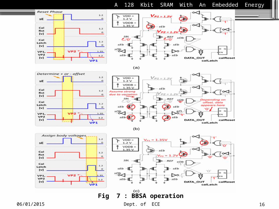
A 128 Kbit SRAM With An Embedded Energy Monitoring Circuit
16Dept. of ECE
Fig 7 : BBSA operation06/01/2015

Dept. of ECE 17
Distribution is 2 times tighter after calibration
A 128 Kbit SRAM With An Embedded Energy Monitoring Circuit
Fig 8 : Measured BBSA input referred offset voltages before and after calibration
06/01/2015
Dept. of ECE 18
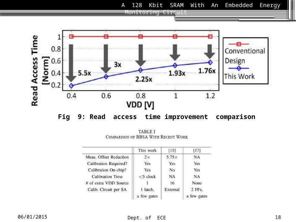
A 128 Kbit SRAM With An Embedded Energy Monitoring Circuit
Fig 9: Read access time improvement comparison
06/01/2015

Dept. of ECE 19
ENERGY-MONITORING CIRCUIT FOR SRAM• Design and methodology
128 kbit SRAM powered by Vsto Vsto: Voltage across Csto Energy sensing is inactive
Energy sensing is active
For correct SRAM operation V1 ≈ V2
o Switch : ONo SRAMs are powered upo Csto supplies charge to SRAMo Vsto starts to drop
o Switch : OFF
A 128 Kbit SRAM With An Embedded Energy Monitoring Circuit
06/01/2015

Dept. of ECE 20
A 128 Kbit SRAM With An Embedded Energy Monitoring Circuit
Fig 10 : Chip block diagram with a focus on the architecture of the energy sensing circuit
06/01/2015

Dept. of ECE 21
• Challenges Effect of ∆V drop on SRAM
Effect of ∆V selection & comparator offset on accuracy
o ∆V drop to be controlled to maintain SRAM stability
o Error associated when V2 approximated to V1
o Relative error due to offset (Vofs)
A 128 Kbit SRAM With An Embedded Energy Monitoring Circuit
Fig 11 : Selection of ∆ V at low voltages for cell stability
06/01/2015

Dept. of ECE 22
o Select high accuracy capacitor with low temperature coefficiento C value should be much larger than parasitic capacitor
Effect of Non- idealities of capacitor
A 128 Kbit SRAM With An Embedded Energy Monitoring Circuit
Fig 12 : Selection of ∆ V for accuracy considerations
06/01/2015

Dept. of ECE 23
MEASUREMENT RESULTS• 128 Kbit 8T bit cell based SRAM is designed
• SRAMs are measured to achieve functionality down to VDD=0.37V
• Energy consumption depends on the
data pattern
• EOP by 3 different methods
• EOP values are scaled down with
voltage scaling
Reading digital EOP output Measuring energy consumption values Transistor-level extracted simulation
A 128 Kbit SRAM With An Embedded Energy Monitoring Circuit
Fig 13 : Die photo of the 128 kb SRAM in 65 nm CMOS
06/01/2015

dA
Dept. of ECE 24
Higher temperature results in larger leakage and larger overall EOP
A 128 Kbit SRAM With An Embedded Energy Monitoring Circuit
Fig 14 : EOP vs VDD graphFig 15 : Measured EOP under different read operation to
write operation ratios and temperatures
06/01/2015

Dept. of ECE 25
CONCLUSION
• SRAMs : Fundamental building block of a system
• Techniques to decrease SRAM energy consumption
• Design memories that can do voltage scaling down
• Low voltage variation problems effecting functionality and
performance
• 2-step sensing scheme with BBSA to increase performance
• Achieves 2*less input offset after calibration
• Energy monitoring circuit is introduced
A 128 Kbit SRAM With An Embedded Energy Monitoring Circuit
06/01/2015

REFERENCES• WEBSITES
ieeexplore.ieee.org/ www.embedded.com
A 128 Kbit SRAM With an Embedded Energy Monitoring Circuit and Sense-Amplifier Offset Compensation Using Body Biasing by Yildiz Sinangil, Member, IEEE, and Anantha P. Chandrakasan, Fellow, IEEE
N. Verma and A. P. Chandrakasan, “A 256 kb 65 nm 8T subthresholdSRAM employing sense-amplifier redundancy,” IEEE J. Solid-StateCircuits (JSSC), vol. 43, no. 1, pp. 141–149, Jan. 2008.
and more....
• PAPERS REFERED
Dept. of ECE 26
A 128 Kbit SRAM With An Embedded Energy Monitoring Circuit
06/01/2015

Dept. of ECE 27
THANK YOU
A 128 Kbit SRAM With An Embedded Energy Monitoring Circuit
06/01/2015

Dept. of ECE 28
QUERIES ????.....
A 128 Kbit SRAM With An Embedded Energy Monitoring Circuit
06/01/2015


