1405 lEEE TRANSACTIONS ON ELECTRON DEVICES, VOL. 35, NO. 9, SEPTEMBER 1988 A High-speed GaAs Error-Detection Circuit for Fiber-optic Transmission Systems Abstract-A high-speed GaAs IC for detection of line code violations is described. This 144-gate error detection circuit for monitoringa high- bit-rate fiber-optic link has been designed and fabricated using a high- yield titanium tungsten nitride self-aligned gate MESFET process. This process routinely provides a wafer-averaged gate delay (fan-in = fan- out = 2) of less than 70 ps with a power dissipation of 0.5 mW/gate. The error-detection circuits were tested on-wafer using high-frequency probe cards at a clock rate of 1.4 GHz, with a yield of 64 percent. Packaged circuits worked at a clock frequency of over 2.5 GHz and consumed 200-mW power at a fixed power supply voltage of 1.5 V. The circuts operate over a wide variation in power supply voltage and tem- perature. When operated at a package temperature of 125”C, the cir- cuits show less than a 12-percent degradation in their maximum clock frequency. The circuit was inserted into a 565-Mbit/s system currently using a silicon ECL part, and full functionality was verified with no necessary modifications. I. INTRODUCTION ECENT development of optical fibers with low-loss R and low-dispersion characteristics has created interest in the development of electronic circuits capable of han- dling multigigabit-per-second data rates. A number of high-speed components, such as directly modulated injec- tion lasers [ 11, detectors [2], and optical pre-amplifiers [3], have been reported. However, digital integrated cir- cuits seem to be the bottleneck for high-bit-rate applica- tions, both at the transmitting and the receiving end of a fiber-optic communication link. The need for higher speed digital communications cir- cuits has focused attention on gallium arsenide (GaAs) technology. GaAs material and fabrication technology is maturing rapidly and demonstrating excellent perfor- mance at respectable yield for MSI [4] and LSI [5] cir- cuits. To realize a multigigabit system, we have devel- oped a number of high-speed GaAs components, including multiplexers, demultiplexers, shift registers, laser driv- ers, and decision and clock recovery circuits. In this pa- per, a high-speed GaAs IC for the detection of line code violations is described. In fiber-optic transmission systems, line codes are used to achieve an equal distribution of marks and spaces in the bit stream, for optimum performance of the receiver Manuscript received February 24, 1988; revised May 6, 1988. This work was supported by the Royal Norwegian Council for Scientific and Industrial Research. The authors are with the ITT Gallium Arsenide Technology Center, Roanoke, VA 24019-1088. IEEE Log Number 8822520. at high speeds and over long distances. The line code adds redundancy to the signal and can be used to monitor the fiber-optic link for bit errors. In high-bit-rate systems, the error-detection circuit must operate at multigigabit data rates and dissipate very little power. The serial nature of the error detection circuit and its few inputs and outputs (I/O’s) make it an ideal candidate for GaAs integration. We have therefore designed, fabricated, and tested a GaAs error-detection circuit. 11. SYSTEM DESCRIPTION The error-detection circuit described here has been de- signed as part of the high-speed fiber-optic link shown in Fig. 1. A fiber-optic transmitter converts the digital data into optical pulses that are transmitted over an optical fi- ber. First, input data in parallel form are converted to a serial bit stream under the control of a clock. The data stream is encoded into the line code and transmitted by a laser over the optical fiber. A fiber-optic receiver extracts the digital data contained in the lightwave signal. Here, the optical pulses are converted back to electrical form in the receiving circuit. A decision circuit then compares the amplified analog signal to a threshold level and decides when the signal represents a logic “1” or a logic “0.” The clock extraction circuit derives the underlying clock- ing frequency from the incoming signal and synchron- ously drives the decision circuit. The data stream is de- coded and then demultiplexed into channels under the control of an internal clock. Due to the attenuation of the optical signal and electri- cal noise in the receiver circuit, the received data may have errors. It is therefore important to monitor the bit error rate (BER) of the data. If the BER is sufficiently high, the data may have to be retransmitted or rerouted through another physical channel. The BER is monitored by counting violations of the line code right at the re- ceiver, making it possible to locate a faulty transmission quickly. However, the high bit rate and the constraints on power dissipation make the design of a good error-detec- tion circuit a challenging task. 111. CIRCUIT DESIGN Various types of binary coding schemes can be used in fiber-optic systems for the purposes of error monitoring, timing recovery, and limiting baseline wander [6]. These binary coding schemes can be broken down into three cat- 0018-9383/88/0900-1405$01 .OO @ 1988 IEEE
Transcript
1405 lEEE TRANSACTIONS ON ELECTRON DEVICES, VOL. 35, NO. 9, SEPTEMBER 1988
A High-speed GaAs Error-Detection Circuit for Fiber-optic Transmission Systems
Abstract-A high-speed GaAs IC for detection of line code violations is described. This 144-gate error detection circuit for monitoring a high- bit-rate fiber-optic link has been designed and fabricated using a high- yield titanium tungsten nitride self-aligned gate MESFET process. This process routinely provides a wafer-averaged gate delay (fan-in = fan- out = 2) of less than 70 ps with a power dissipation of 0.5 mW/gate. The error-detection circuits were tested on-wafer using high-frequency probe cards at a clock rate of 1.4 GHz, with a yield of 64 percent. Packaged circuits worked at a clock frequency of over 2.5 GHz and consumed 200-mW power at a fixed power supply voltage of 1.5 V. The circuts operate over a wide variation in power supply voltage and tem- perature. When operated at a package temperature of 125”C, the cir- cuits show less than a 12-percent degradation in their maximum clock frequency. The circuit was inserted into a 565-Mbit/s system currently using a silicon ECL part, and full functionality was verified with no necessary modifications.
I. INTRODUCTION ECENT development of optical fibers with low-loss R and low-dispersion characteristics has created interest
in the development of electronic circuits capable of han- dling multigigabit-per-second data rates. A number of high-speed components, such as directly modulated injec- tion lasers [ 11, detectors [2], and optical pre-amplifiers [3], have been reported. However, digital integrated cir- cuits seem to be the bottleneck for high-bit-rate applica- tions, both at the transmitting and the receiving end of a fiber-optic communication link.
The need for higher speed digital communications cir- cuits has focused attention on gallium arsenide (GaAs) technology. GaAs material and fabrication technology is maturing rapidly and demonstrating excellent perfor- mance at respectable yield for MSI [4] and LSI [5] cir- cuits. To realize a multigigabit system, we have devel- oped a number of high-speed GaAs components, including multiplexers, demultiplexers, shift registers, laser driv- ers, and decision and clock recovery circuits. In this pa- per, a high-speed GaAs IC for the detection of line code violations is described.
In fiber-optic transmission systems, line codes are used to achieve an equal distribution of marks and spaces in the bit stream, for optimum performance of the receiver
Manuscript received February 24, 1988; revised May 6, 1988. This work was supported by the Royal Norwegian Council for Scientific and Industrial Research.
The authors are with the ITT Gallium Arsenide Technology Center, Roanoke, VA 24019-1088.
IEEE Log Number 8822520.
at high speeds and over long distances. The line code adds redundancy to the signal and can be used to monitor the fiber-optic link for bit errors. In high-bit-rate systems, the error-detection circuit must operate at multigigabit data rates and dissipate very little power. The serial nature of the error detection circuit and its few inputs and outputs (I/O’s) make it an ideal candidate for GaAs integration. We have therefore designed, fabricated, and tested a GaAs error-detection circuit.
11. SYSTEM DESCRIPTION The error-detection circuit described here has been de-
signed as part of the high-speed fiber-optic link shown in Fig. 1. A fiber-optic transmitter converts the digital data into optical pulses that are transmitted over an optical fi- ber. First, input data in parallel form are converted to a serial bit stream under the control of a clock. The data stream is encoded into the line code and transmitted by a laser over the optical fiber. A fiber-optic receiver extracts the digital data contained in the lightwave signal. Here, the optical pulses are converted back to electrical form in the receiving circuit. A decision circuit then compares the amplified analog signal to a threshold level and decides when the signal represents a logic “1” or a logic “0.” The clock extraction circuit derives the underlying clock- ing frequency from the incoming signal and synchron- ously drives the decision circuit. The data stream is de- coded and then demultiplexed into channels under the control of an internal clock.
Due to the attenuation of the optical signal and electri- cal noise in the receiver circuit, the received data may have errors. It is therefore important to monitor the bit error rate (BER) of the data. If the BER is sufficiently high, the data may have to be retransmitted or rerouted through another physical channel. The BER is monitored by counting violations of the line code right at the re- ceiver, making it possible to locate a faulty transmission quickly. However, the high bit rate and the constraints on power dissipation make the design of a good error-detec- tion circuit a challenging task.
111. CIRCUIT DESIGN Various types of binary coding schemes can be used in
fiber-optic systems for the purposes of error monitoring, timing recovery, and limiting baseline wander [6]. These binary coding schemes can be broken down into three cat-
0018-9383/88/0900-1405$01 .OO @ 1988 IEEE
1406 IEEE TR LANSACTIONS ON ELECTRON DEVICES, VOL. 35, NO. 9, SEPTEMBER 1988
Encoder mitter
Optical Fiber
jylI...H-Z-h
Fig. 1. Block diagram of a high-speed fiber-optic transmission system
Test Outputs
4444 Error Pulse Generator
GaAs
Reset
Fig. 2. Schematic of the error-detection circuit,
3 Flag output
egories: scrambled binary codes, bit insertion codes, and block codes [7]. Unlike scrambling and bit insertion, block coding allows bit sequence independence. The er- ror-detection circuit described here uses block coding or “mBnB coding. ” Binary block coding adds redundancy to the data stream, and is particularly suited to fiber-optic systems, which generally use on-off binary modulation. The coding efficiency (m/n) is the ratio of the actual to the theoretical information rate corresponding to that sig- naling alphabet and pulse rate. For example, in Man- chester coding ( 1 B2B), the coding efficiency is 50 per- cent. The error-detection circuit described here is based on 5B6B coding, which results in a much higher effi- ciency of 83 percent.
Some of the limiting factors with block coding are: complex encoder and decoder circuits, a delay of m clock periods between data entering and exiting the coder, and a clock frequency at least n/m times the data rate.
The overall error-detection circuit is depicted in Fig. 2 and is similar to one implemented in silicon technology. Fig. 3 shows the internal operation of the error pulse gen- erator. The circuit consists of a 6-bit left/right shift reg- ister, a four-stage divider, a digital one-shot, and GaAs and ECL interfaces. In addition, four test outputs are in- cluded to verify circuit functionality. To effectively detect an error, this detector relies on the running digital sum variation property (DSV) of the 5B6B code. The DSV of valid register states is shown in Table I, where DSV = - 3 + C :z D;. If the DSV exceeds plus or minus three, an error pulse will be generated. The 5 B6B code is chosen
so that there is no code or combination of shifting codes into registers D1 through 0 6 for which the DSV exceeds + 3 or - 3. Initially , the shift register is preset so the DSV equals zero. Next, register DO synchronizes the incoming data with the clock. If a logic “1” is loaded into register DO, then the contents of registers D1 through 0 6 will be shifted to the right. However, if a logic “0” gets loaded into DO, then the contents of registers D 1 through 0 6 will be shifted to the left. In other words, an error will be gen- erated when a logic “0” gets loaded into DO and registers DO and 0 2 are both at a logic “0” or when a logic “ 1 ” gets loaded into DO and register DO and D5 are both at a logic “1.” This coincides with the DSV < -3 or DSV > +3. When an error occurs, the output of 0 7 generates a digital one-shot. A four-stage divider is utilized to broaden this pulse so it can be used by a microprocessor controlling the system.
To obtain high-speed operation at lower power dissi- pation, GaAs enhancement/depletion direct-coupled FET logic (E/D DCFL) is used [8], [9]. This circuit approach is similar to silicon NMOS. It requires only one power supply, and employs only a depletion-mode (DFET) pull- up and enhancement-mode (EFET) pull-down transistor, without the need for a level-shifting stage.
Basic building blocks, such as E/D DCFL logic gates, D-type flip-flops, ECL-to-GaAs and GaAs-to-ECL trans- lators, and drivers were first designed. The gate design was optimized to provide equal rise and fall times with the switching point at the midpoint of the logic swing. The edge-triggered D-type flip-flop was optimized for maximum speed and minimum power dissipation, while keeping the minimum width of the switching FET at 20 pm. Translators and drivers were optimized to provide the correct rise and fall times and output swing under practi- cal loading. The error-detection circuit was designed and laid out using these previously optimized components, and it features selectable built-in silicon ECL and GaAs-com- patible I/O interfaces. In addition, to improve testability, four test outputs are included on the chip. The complete circuit was extensively simulated with SPICE, including all measured interconnection parasitics.
IV. FABRICATION PROCESS The circuits are fabricated with a titanium tungsten ni-
tride (TiWN) self-aligned gate process as illustrated in Fig. 4. This fully planar process employs selective ion implementation into 2-in undoped LEC substrates. The substrates are first passivated with 850 A of plasma-de- posited silicon oxynitride (SON), through which selec- tive 29Si implants are performed for EFET and DFET ac- tive channels. The SjON passivation layer is then re- moved, and a 2000-A layer of TiWN is deposited by reactive sputtering.
The TiWN layer is patterned into “T-gate” structures by lift-off of a Ni etch mask and subsequent reactive-ion etching. A self-aligned n+ implant is then performed, and after removal of the Ni mask, the wafer is capped with SiON and annealed at 810°C for 20 min. To maximize
SINGH et ai.: HIGH-SPEED GaAs ERROR-DETECTION CIRCUIT
OSV
1407
01 D 2 03 D4 0 5 06
DATA IN
CL ERROR
.OCK RESET DETECTION
Fig. 3. Schematic of the error pulse generator
TABLE I POSSIBLE SHIFT REGISTER STATES AND DIGITAL SUM VARIATIONS
+ 3
+ 2
+ 1
0
- 1
- 2
- 3
1 0 0
implant activation, we have optimized the composition and stress in the SiON anneal cap, which has a refractive index n = 1.55.
After annealing, ohmic contacts are formed by lift-off and alloying of AuGe/Ni. The circuits are then com- pleted by defining twoo levels of interconnect metalliza- tion, each using 6000 A of Ti/Pd/Au patterned by lift- off. The interconnect levels are separated by 1 pm of polyimide, for low-capacitance crossovers. Sheet resis- tance of the interconnect metal is 0.06 Q/sq, and via re- sistance for a 3 pm x 3 pm contact between first- and second-level metal is 0.09 Q .
V. DEVICE AND CIRCUIT PERFORMANCE Typical drain characteristics of an enhancement-mode
MESFET, or EFET, are shown in Fig. 5. The gate length and gate width are 1 and 20 pm, respectively. The EFET devices have a threshold voltage VT = +0.1 V, with a standard deviation of 25 mV over a 2-in wafer. Their wafer-averaged transconductance is typically 230 mS /mm (measured at V,, = +0.6 V, V,, = 1 V ), with a standard deviation over the wafer of 4 percent of the mean. The depletion-mode FET devices have V, = -0.5 V, with the standard deviation of 45 mV. Their transconductance is typically 175 mS/mm (measured at V,, = 0 V, V,, = 1 V).
1408 IEEE TRANSACTIONS ON ELECTRON DEVICES, VOL. 3.5, NO. 9, SEPTEMBER 1988
0 05 1 0 1.5 2 0
vDS
Fig. 5. Drain characteristics of a typical EFET with gate length of 1 pm and width of 20 pm. Vcs = 0 to +0.6 V in steps of 0.1 V.
All gates, D-type flip-flops, translators, and drivers were tested individually on wafers using probe cards. The gate characteristics of a NOR gate are shown in Fig. 6 . It has a switching point at 0.39 V, with low and high noise margins in excess of 250 mV at a power supply voltage VDD = 1.2 V. From ring oscillator measurements, a wafer- averaged gate delay of 66 ps and a power dissipation of 0.5 mW/gate is obtained for a fan-in fan-out of 2. Di- vide-by-two circuits using a D-type flip-flop have been evaluated on these wafers. The frequency divider worked up to 2.8 GHz and consumed 3.1 mW power at a power supply voltage of 1.2 V, as illustrated in Fig. 7.
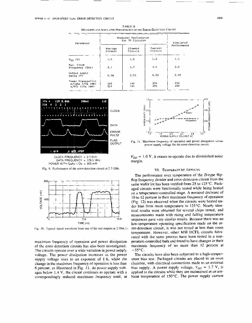
The microphotograph of the fabricated error-detection circuit is shown in Fig. 8. The chip size is 1.73 X 1.24 mm including all translators, drivers, and bonding pads. The error-detection circuits were tested on-wafer with a fixed 1.4-GHz test pattern using high-frequency probe cards. This test showed a yield of 191/300 (64 percent) for a typical wafer, which was then chosen for further testing. After dicing the wafer, 30 parts were packaged and tested for their maximum frequency of operation. All of them were tested with a 1.5 V power supply, and the results are summarized in Table 11. For the 30 circuits, the maximum clock frequency varied between 1.7 and 2.5 GHz, with a mean value of 2.1 GHz, while the power dissipation ranged from 140 to 200 mW using GaAs-com- patible interfaces. The average measured output logic swing was about 0.58 V, while the simulated logic swing was 0.80 V. The discrepancy can be attributed mainly to the attenuation of the probe card. For example, the pre- viously measured power loss on some randomly selected probe cards was 2 to 3 dB at 2 GHz. Therefore, compen- sating for probe card loss gives an output voltage swing of 0.73 to 0.82 V, which agrees quite well with the sim- ulated output swing of 0.80 V.
Fig. 9 shows the performance of the error-detection cir- cuit at a 2.5-GHz clock frequency. A data rate of 1/14 of the clock rate was chosen in order to depict an error pulse. Since the DSV exceeds & 3 , an error is indeed in- dicated. The maximum data,rate is 5/6 times the clock rate, or 2.08 GHz. However, our test equipment did not allow true synchronization between the clock and data for data rates exceeding 2 GHz. Therefore, the highest clock frequency possible may be somewhat higher than the 2.5 GHz shown in Fig. 9.
L
0.8 -
0.2 -
I I I I I I I ,
Vin. Vout (V)
'0 0.2 0:4 0.6 0.8 1
Fig. 6 . NOR gate transfer characteristics, V,,,, = 1.2 V
Fig. 8. Microphotograph of the fabricated error-detection circuit
The circuits have also been tested with realistic data patterns at different frequencies, and the circuit outputs were found to be stable and noise-free under all input data combinations. Fig. 10 shows a typical signal waveform from one of the four test outputs when tested at 2 GHz. As can be seen, the pulses have good rise and fall times and the logic levels are stable.
The effect of power supply voltage variation on the
SlNGH et ai.: HIGH-SPEED GaAs ERROR-DETECTION CIRCUIT
~
1409
TABLE I1 MEASURED A N D SIMULATED PERFORMANCE OF THE ERROR-DETECTION CIRCUIT
I M e
Max. C l o c k F r e q u e n c y (GHz) 2 . 5 I 2.0 I O u t p u t Logic Swing ( V ) I 0.56 1 0.53 I 0.54 I 0.80
Power D i s s i p a t i o n w/GaAs I/Os LmW) w/ECL I / O s (mW)
CLOCK FREQUENCY = 2.5 GHz DATA FREQUENCY = 178 5 MHz
POWER WITH GaAs I I Os = 200 mW
Fig. 9. Performance of the error-detection circuit at 2 .5 GHz.
5.0 10.0
TIME (ns)
Fig. 10. Typical signal waveform from one of the test outputs at 2 Gbit/s.
maximum frequency of operation and power dissipation of the error-detection circuits has also been investigated. The circuits operate over a wide variation in power supply voltage. The power dissipation increases as the power supply voltage rises to an exponent of 1.6, while the change in the maximum frequency of operation is less than 6 percent, as illustrated in Fig. 11. At power supply volt- ages below 1.4 V, the circuit continues to operate with a correspondingly reduced maximum frequency until, at
1 0 1'2 1'6 2'0 2'4 2'8 3:'
POWER SUPPLY VOLTAGE (V)
Fig. 11. Maximum frequency of operation and power dissipation versus power-supply voltage for the error-detection circuit.
V,, = 1 .O V , it ceases to operate due to diminished noise margin.
VI. TEMPERATURE EFFECTS The performance over temperature of the D-type flip-
flop frequency divider and error-detection circuit from the same wafer lot has been verified from 25 to 125°C. Pack- aged circuits were functionally tested while being heated on a temperature-controlled stage. A nominal decrease of 10 to 12 percent in their maximum frequency of operation (Fig. 12) was observed when the circuits were heated un- der bias from room temperature to 125°C. Nearly iden- tical results were obtained for several chips tested, and measurements made with rising and falling temperature sequences gave very similar results. Because there was no low-temperature operating specification made on the er- ror-detection circuit, it was not tested at less than room temperature. However, other MSI DCFL circuits fabri- cated with the same process have been tested in a tem- perature-controlled bath and found to have changes in their maximum frequency of no more than 12 percent at -55°C.
The circuits have also been subjected to a high-temper- ature bias test. Packaged circuits are placed in an oven chamber, with electrical connections made to an external bias supply. A power supply voltage, VDD = 1.7 V , is applied to the circuits while they are maintained at an am- bient temperature of 150°C. The power supply current
1410 IEEE TRANSACTIONS ON ELECTRON DEVICES, VOL. 35. NO. 9. SEPTEMBER 1988
”0 25 50 75 100 125 TEMPERATURE ( “C)
formance. The circuit was verified to be fully functional as a drop-in replacement in a 565-Mbit/s fiber-optic link.
ACKNOWLEDGMENT The authors thank A. E. Geissberger, E. L. Griffin, and
D. G. Fisher for their valuable support and K. Stokes for high-speed testing. They would like to thank Prof. I. Ja- cobs of the Virginia Polytechnic Institute for his valuable discussions. Thev also wish to thank Standard Elektrik
50
Fig. 12. Effect of temperature on maximum frequency of operation for D- type flip-flop divider and error detection circuit.
L~~~~~ AG for supplying information about their silicon version of the circuit.
Zoo drawn by the circuits is recorded by a computer at 1-h intervals. The circuits are periodically removed from the oven and tested for high-frequency performance. After a cumulative storage for 3200 h at 15OoC, less than a 1- percent change in both high-frequency performance and in power supply current has been observed for these cir- cuits.
VII. COMPARISON OF GaAs AND SILICON ERROR- DETECTION CIRCUITS
The GaAs error-detection circuit was inserted into a 565-Mbit / s fiber-optic link developed by Standard Elek- trik Lorenz AG (SEL) in Germany for trunking applica- tions. The currently existing system uses a silicon ECL error-detection circuit. The GaAs circuit was inserted into the system and full functionality was ascertained with no necessary modifications. Hence, the GaAs error-detection circuit can be used as a drop-in replacement for the silicon ECL circuit.
The performance of the GaAs error-detection circuit can be compared with the equivalent silicon ECL version [ 101. The clock frequency and power consumption of the GaAs version (2.1 GHz, 214 mW) are both superior to that of I
REFERENCES [ I ] J . E. Bowers, B. R. Hemenway, A. K. Gnauck, T . J. Bridges, E. G.
Burkhardt, D. P. Wilt, and S. Maynard, “High-frequency constricted mesa lasers,” Appl. Phys. Lett . , vol. 47, pp. 78-80, 1985.
[2] S. Y. Wang and D. M. Bloom, “100 GHz bandwidth planar GaAs Schottky photodiode,” Electron. Lett . , vol. 19, no. 14, July 7 , 1983.
[3] Y. Archambault, D. Pavlidis, and J. Guet, “GaAs monolithic inte- grated optical preamplifier,” J. Lightwave Technol., vol. LT-5, no.
[4] H. P. Singh, R. A. Sadler, A. E. Geissberger, W. J. Tanis, and E. R. Schineller, “High speed, low-power GaAs programmable counters for synthesizer applications,” in Proc. IEEE GuAs ICSymp., pp. 269- 272, 1987.
[5] H. P. Singh, R. A. Sadler, J . A. Irvine, and G. E. Gorder, “GaAs low-power parallel multipliers for a high-speed signal processor, ” in Proc. IEEE GaAs IC Symp., pp. 253-256, 1987.
[6] I . Jacobs, “Design considerations for long-haul lightwave systems,” IEEEJ. Select. Areas Commun., vol. SAC-4, no. 9 , pp. 1389-1395, Dec. 1986.
171 N. Yoshikai, S. Nishi, and J. Yamada, “Line code and terminal con- figuration for very large-capacity optical transmission system,” lEEE J . Select. Areas Commun., vol. SAC-4, no. 9 , pp. 1432-1437, Dec. 1986.
[8] R. E. Lundgren, C. F. Krumm, and R. F. Lohr, Jr., presented at the GaAs Integration Circuit Symp., Lake Tahoe, CA, Sept. 1979.
[9] H. P. Singh, R. A. Sadler, A. E. Geissberger, D. G. Fisher, J . A. Irvine, and G. E. Gorder, “A comparative study of GaAs logic tam- ilies using universal shift registers and self-aligned gate technology ,” in Proc. IEEE GaAs IC Symp., pp. 11-14, 1986.
3, pp. 355-366, 1987.
[lo] Standard Elektrik Lorentz AG, unpublished test results, 1986. the silicon version ( 1 GHz, 1.2 W). The silicon error- detection circuit has a power-delay product 12 times higher than the GaAs version described here. In a system environment, due to its higher power dissipation, the sil- icon circuit needs a heat-sink arrangement, whereas the GaAs version does not require any heat-sink fixturing.
VIII. CONCLUSION Using GaAs self-aligned gate technology, a 144-gate
error-detection circuit for monitoring a high-bit-rate fiber- optic link has been designed, fabricated, and extensively tested at room temperature and above. The circuits were tested on-wafer at room temperature using high-frequency probe cards at a clock rate of 1.4 GHz, with a yield of 64 percent. Packaged circuits worked at a clock frequency of over 2.5 GHz and consumed only 200 mW power at a fixed power supply voltage of 1.5 V. When operated at a package temperature of 125”C, these circuits showed less then a 12-percent degradation in their maximum clock frequency. The circuits subjected to 3200 h of storage un- der bias at an ambient temperature of 15OoC, showed less than a 1-percent degradation in their high-frequency per-
*
Hausila P. Singh (M’81-SM’88) was born in Varanasi, India, in 1942 He received the B.S de- gree with honors, the M S . degree in physics, and the Ph.D degree in solid state physics from the Banaras Hindu University, India, in 1963, 1965, and 1968, respectively
He was with the Birla Institute of Technology and Science, Pilana, India, from 1968 to 1969 where he taught courses in physics. He waq a Postdoctoral Research Fellow at the Massachu- setts Institute of Technology, Cambridge, and at
the University of Southern California, Los Angeles, from 1969 to 1972 He spent six years as a Reader in Physics at Punjabi University, India, where he taught graduate courses in solid state physics and was engaged in research of the electrical properties of metal-insulator and metal-semi- conductor devices. From 1978 to 1982, he was associated with Wright Patterson Air Force Base, Dayton, Ohio, as a Senior Visiting Scientist. where he was involved in the research and development of high-speed dig- ita1 circuits utilizing GaAs insulated-gate FET’s. He joined the ITT Gal- lium Arsenide Technology Center, Roanoke, VA, in 1982 as Senior Prin- cipal Scientist. In his current position as Technical Staff Fellow, he is responsible for the design and testing of high-speed GaAs digital circuits.
SINGH et d.: HIGH-SPEED GaAs ERROR-DETECTION CIRCUIT 141 1
He is the author or co-author of more than 75 research papers and technical reports.
Dr. Singh was awarded a Certificate of Recognition by the Electron Mi- croscopy Society of America in 1972 for Best Physical Science Applica- tion, “An Electron Microscope Study of Vapor-Liquid-Solid Growth in In and Sn Thin Films.”
John F. Naber (S’81-M’85) was born in Phila- delphia, PA, in 1961. He received the B.S. degree in electncal engineenng in 1983, and the M.E. degree in electrical engineenng in 1985, both from the University of Louisville. He is currently working toward the Ph.D. degree at Virginia Polytechnic University. His Master’s thesis was on the quantum efficiency of silicon UV photo- diodes using edge illumination.
He joined General Electnc in 1985 where he worked on GaAs analog-to-digital converters and
* digital-to-analog converters. In 1987, he joined ;he ITT Gallium Arsenide Technology Center, Roanoke, VA, as a GaAs digital designer, and is cur- rently responsible for several digital and analog projects.
Mr. Naber is a member of Tau Beta Pi.
* Robert A. Sadler (S’76-M’84) was born at Fort Campbell, Kentucky, on February 1, 1954. He re- ceived the B.S and M.S. degrees in electrical en- gineenng from North Carolina State University, Raleigh, in 1978 and 1980, respectively, and the Ph.D. degree in electrical engineering from Cor- ne11 University, Ithaca, NY, in 1984. His doctoral research was on submicrometer-gate self-aligned GaAs MESFET’s for digital IC’s.
While at Cornell, he was a Howard Hughes Doctoral Fellow at the Hughes Research Labora-
tones, Malibu, CA, where he worked on electron-beam lithography and the early development of refractory self-aligned gate fabncation technol- ogy. In 1984, he joined the ITT Gallium Arsenide Technology Center, Roanoke, VA, with responsibility for GaAs materials and selective ion im- plantation process development. His present responsibilities include digital IC fabrication and advanced device development. He has authored or co- authored more than 30 technical papers on GaAs devices and materials.
Bard 0. Johannessen was born in Bodo, Nor- way, in 1960. He received the “Sivilingenior” degree from the Department of Electronics at the Norwegian Institute of Technology, Trondheim, in 1983. His thesis was about the design and sim- ulation of a GaAs high-speed gate array.
He spent one year at the Norwegian Defense Research Establishment, working with the design and layout of NMOS custom integrated circuits. He joined the broad-band communications group at Alcatel-STK’s research center in Oslo in 1985,
where he worked on high-speed fiber-optic transmission systems and on digital GaAs IC technology. He participated in a project on a GaAs stan- dard cell library. Later, as a member of the fiber-optics group, he worked on a coherent fiber-optic transmission system where heterodyne receivers and DFB lasers were used. Since April 1988, he has been with EB Net- corn’s Defense Division in Billingstad, Norway, where he IS a Systems Engineer. Dr. Sadler is a member of the Amencan Vacuum Society.