58
A. Kahng, EDA Forum 2003 Keynote, 031106 The Design-Manufacturing Roadmap Andrew B. Kahng UC San Diego CSE & ECE Departments http://vlsicad.ucsd.edu
| Date post: | 19-Dec-2015 |
| Category: |
Documents |
| View: | 218 times |
| Download: | 0 times |
A. Kahng, EDA Forum 2003 Keynote, 031106
The Design-Manufacturing Roadmap
Andrew B. KahngUC San Diego CSE & ECE Departmentshttp://vlsicad.ucsd.edu
A. Kahng, EDA Forum 2003 Keynote, 031106
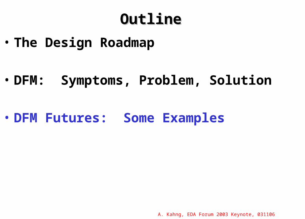
OutlineOutline
• The Design Roadmap
• DFM: Symptoms, Problem, Solution
• DFM Futures: Some Examples
A. Kahng, EDA Forum 2003 Keynote, 031106
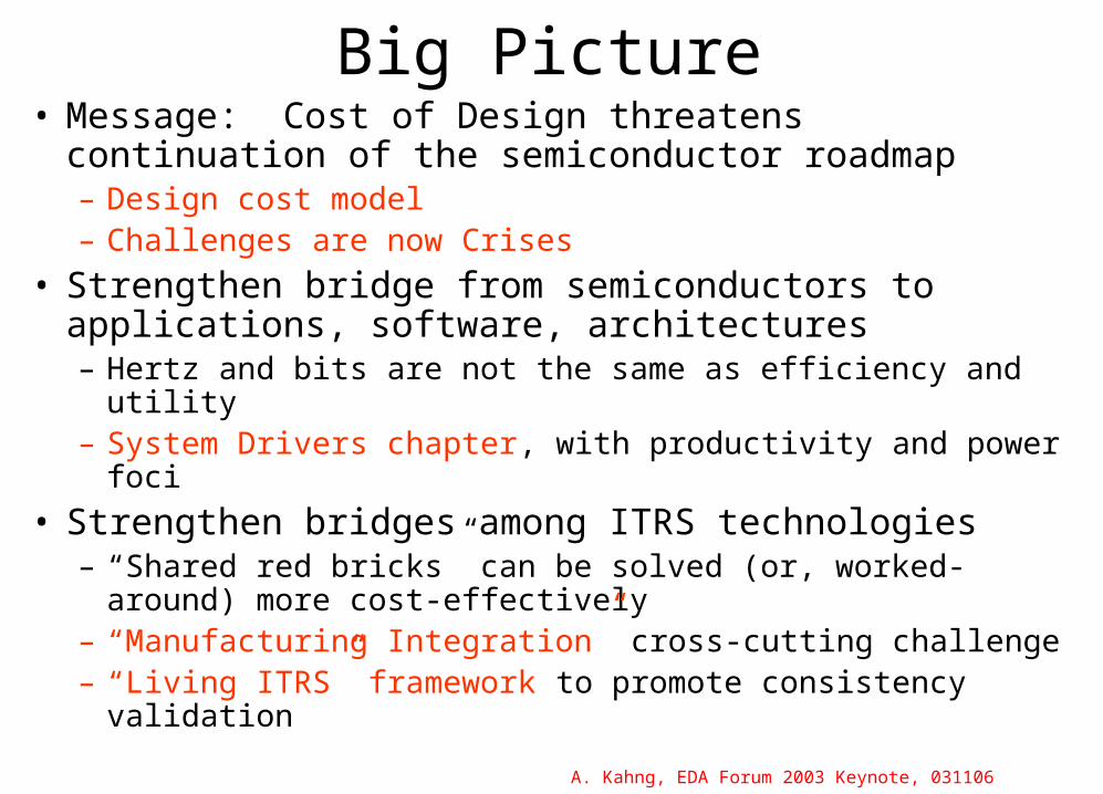
Big Picture• Message: Cost of Design threatens continuation of the
semiconductor roadmap– Design cost model– Challenges are now Crises
• Strengthen bridge from semiconductors to applications, software, architectures– Hertz and bits are not the same as efficiency and utility– System Drivers chapter, with productivity and power foci
• Strengthen bridges among ITRS technologies– “Shared red bricks” can be solved (or, worked-around) more
cost-effectively– “Manufacturing Integration” cross-cutting challenge– “Living ITRS” framework to promote consistency validation
A. Kahng, EDA Forum 2003 Keynote, 031106
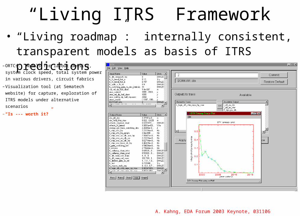
“Living ITRS” Framework
– ORTCs: Models for layout density,
system clock speed, total system power
in various drivers, circuit fabrics
– Visualization tool (at Sematech website)
for capture, exploration of ITRS models
under alternative scenarios
– “Is --- worth it?”
• “Living roadmap”: internally consistent, transparent models as basis of ITRS predictions
A. Kahng, EDA Forum 2003 Keynote, 031106
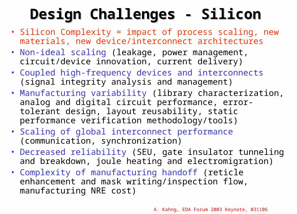
Design Challenges - SiliconDesign Challenges - Silicon• Silicon Complexity = impact of process scaling, new materials,
new device/interconnect architectures• Non-ideal scaling (leakage, power management, circuit/device
innovation, current delivery)• Coupled high-frequency devices and interconnects (signal
integrity analysis and management)• Manufacturing variability (library characterization, analog and
digital circuit performance, error-tolerant design, layout reusability, static performance verification methodology/tools)
• Scaling of global interconnect performance (communication, synchronization)
• Decreased reliability (SEU, gate insulator tunneling and breakdown, joule heating and electromigration)
• Complexity of manufacturing handoff (reticle enhancement and mask writing/inspection flow, manufacturing NRE cost)
A. Kahng, EDA Forum 2003 Keynote, 031106
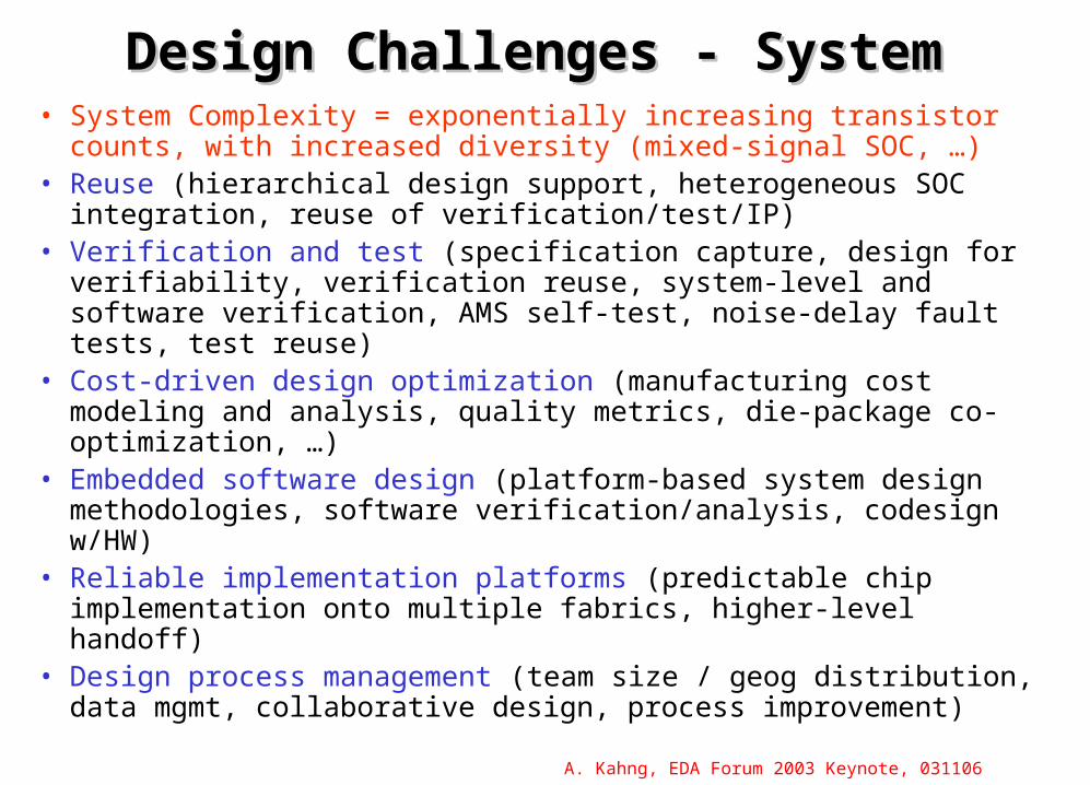
Design Challenges - SystemDesign Challenges - System• System Complexity = exponentially increasing transistor
counts, with increased diversity (mixed-signal SOC, …)• Reuse (hierarchical design support, heterogeneous SOC
integration, reuse of verification/test/IP)• Verification and test (specification capture, design for
verifiability, verification reuse, system-level and software verification, AMS self-test, noise-delay fault tests, test reuse)
• Cost-driven design optimization (manufacturing cost modeling and analysis, quality metrics, die-package co-optimization, …)
• Embedded software design (platform-based system design methodologies, software verification/analysis, codesign w/HW)
• Reliable implementation platforms (predictable chip implementation onto multiple fabrics, higher-level handoff)
• Design process management (team size / geog distribution, data mgmt, collaborative design, process improvement)
A. Kahng, EDA Forum 2003 Keynote, 031106
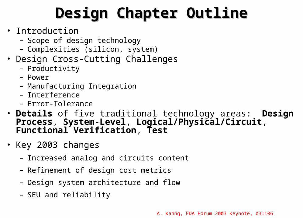
Design Chapter OutlineDesign Chapter Outline• Introduction
– Scope of design technology– Complexities (silicon, system)
• Design Cross-Cutting Challenges– Productivity– Power– Manufacturing Integration– Interference– Error-Tolerance
• Details of five traditional technology areas: Design Process, System-Level, Logical/Physical/Circuit, Functional Verification, Test
• Key 2003 changes– Increased analog and circuits content
– Refinement of design cost metrics
– Design system architecture and flow
– SEU and reliability
A. Kahng, EDA Forum 2003 Keynote, 031106
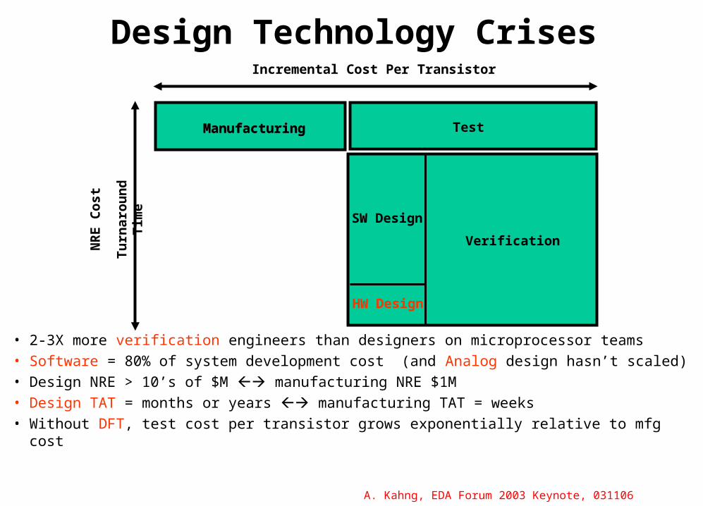
Design Technology Crises
Manufacturing
NR
E C
ost
SW Design
Verification
HW Design
TestT
urn
aro
un
d T
ime
Manufacturing
Incremental Cost Per Transistor
• 2-3X more verification engineers than designers on microprocessor teams
• Software = 80% of system development cost (and Analog design hasn’t scaled)
• Design NRE > 10’s of $M manufacturing NRE $1M
• Design TAT = months or years manufacturing TAT = weeks
• Without DFT, test cost per transistor grows exponentially relative to mfg cost
A. Kahng, EDA Forum 2003 Keynote, 031106
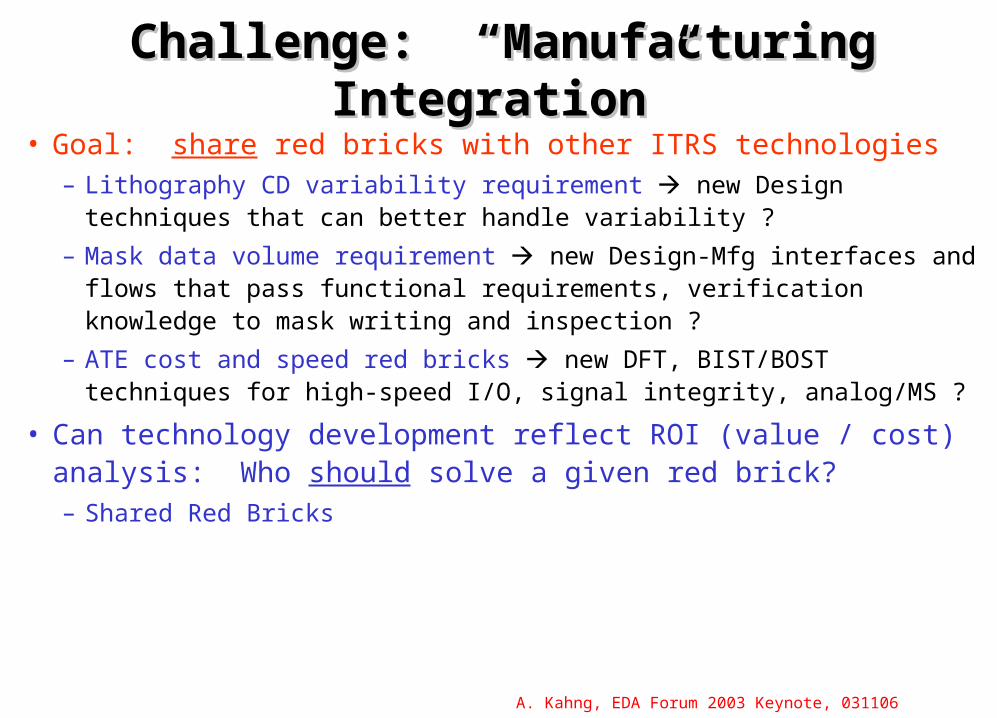
Challenge: “Manufacturing Integration”Challenge: “Manufacturing Integration”
• Goal: share red bricks with other ITRS technologies– Lithography CD variability requirement new Design techniques
that can better handle variability ?
– Mask data volume requirement new Design-Mfg interfaces and flows that pass functional requirements, verification knowledge to mask writing and inspection ?
– ATE cost and speed red bricks new DFT, BIST/BOST techniques for high-speed I/O, signal integrity, analog/MS ?
• Can technology development reflect ROI (value / cost) analysis: Who should solve a given red brick? – Shared Red Bricks
A. Kahng, EDA Forum 2003 Keynote, 031106
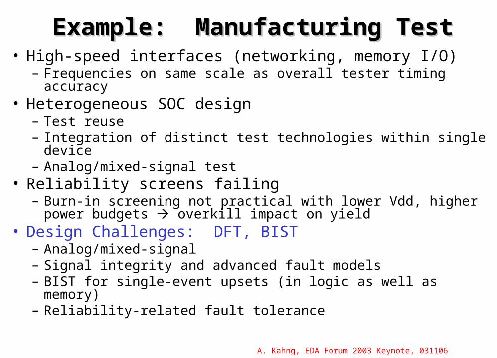
Example: Manufacturing TestExample: Manufacturing Test• High-speed interfaces (networking, memory I/O)
– Frequencies on same scale as overall tester timing accuracy• Heterogeneous SOC design
– Test reuse– Integration of distinct test technologies within single device– Analog/mixed-signal test
• Reliability screens failing– Burn-in screening not practical with lower Vdd, higher power
budgets overkill impact on yield• Design Challenges: DFT, BIST
– Analog/mixed-signal– Signal integrity and advanced fault models– BIST for single-event upsets (in logic as well as memory)– Reliability-related fault tolerance
A. Kahng, EDA Forum 2003 Keynote, 031106
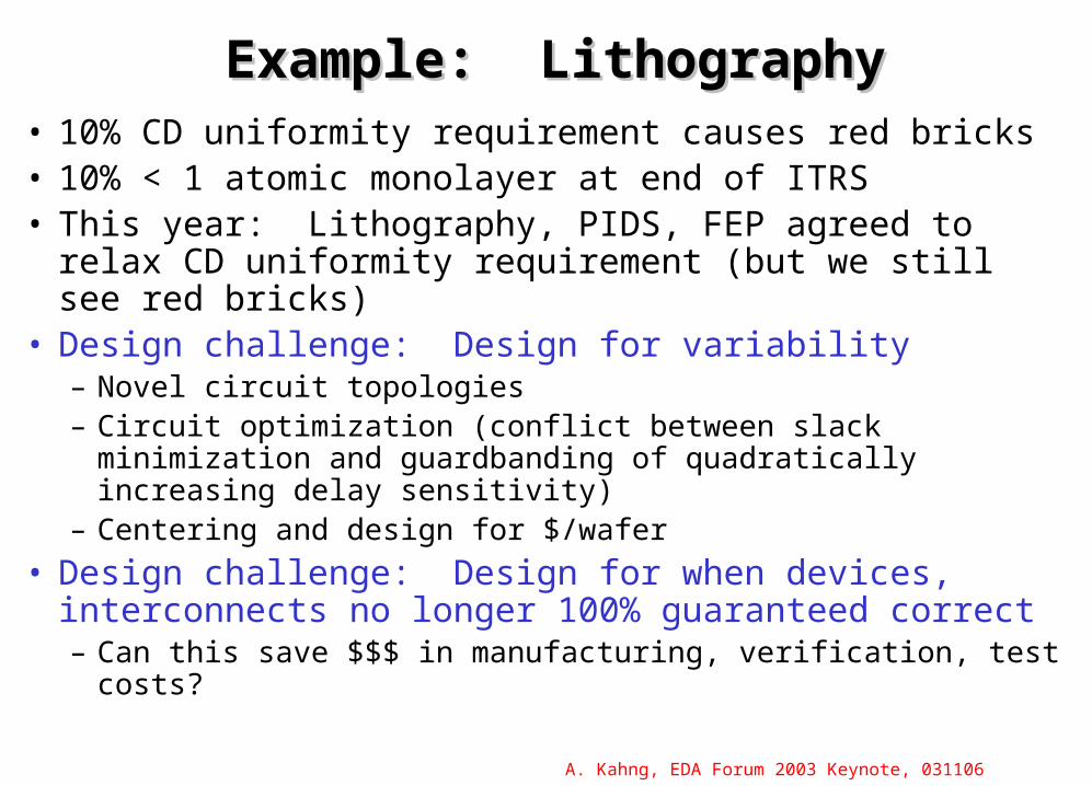
Example: LithographyExample: Lithography• 10% CD uniformity requirement causes red bricks• 10% < 1 atomic monolayer at end of ITRS• This year: Lithography, PIDS, FEP agreed to relax CD
uniformity requirement (but we still see red bricks)• Design challenge: Design for variability
– Novel circuit topologies– Circuit optimization (conflict between slack minimization and
guardbanding of quadratically increasing delay sensitivity)– Centering and design for $/wafer
• Design challenge: Design for when devices, interconnects no longer 100% guaranteed correct– Can this save $$$ in manufacturing, verification, test costs?
A. Kahng, EDA Forum 2003 Keynote, 031106
OutlineOutline
• The Design Roadmap
• DFM: Symptoms, Problem, Solution
• DFM Futures: Some Examples
A. Kahng, EDA Forum 2003 Keynote, 031106
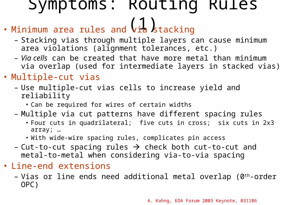
Symptoms: Routing Rules (1)• Minimum area rules and via stacking
– Stacking vias through multiple layers can cause minimum area violations (alignment tolerances, etc.)
– Via cells can be created that have more metal than minimum via overlap (used for intermediate layers in stacked vias)
• Multiple-cut vias– Use multiple-cut vias cells to increase yield and reliability
• Can be required for wires of certain widths
– Multiple via cut patterns have different spacing rules• Four cuts in quadrilateral; five cuts in cross; six cuts in 2x3 array; …• With wide-wire spacing rules, complicates pin access
– Cut-to-cut spacing rules check both cut-to-cut and metal-to-metal when considering via-to-via spacing
• Line-end extensions– Vias or line ends need additional metal overlap (0th-order OPC)
A. Kahng, EDA Forum 2003 Keynote, 031106
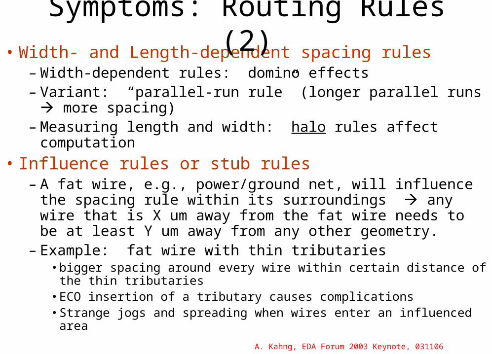
• Width- and Length-dependent spacing rules– Width-dependent rules: domino effects– Variant: “parallel-run rule” (longer parallel runs more
spacing)– Measuring length and width: halo rules affect computation
• Influence rules or stub rules– A fat wire, e.g., power/ground net, will influence the spacing
rule within its surroundings any wire that is X um away from the fat wire needs to be at least Y um away from any other geometry.
– Example: fat wire with thin tributaries• bigger spacing around every wire within certain distance of the thin
tributaries• ECO insertion of a tributary causes complications• Strange jogs and spreading when wires enter an influenced area
Symptoms: Routing Rules (2)
A. Kahng, EDA Forum 2003 Keynote, 031106
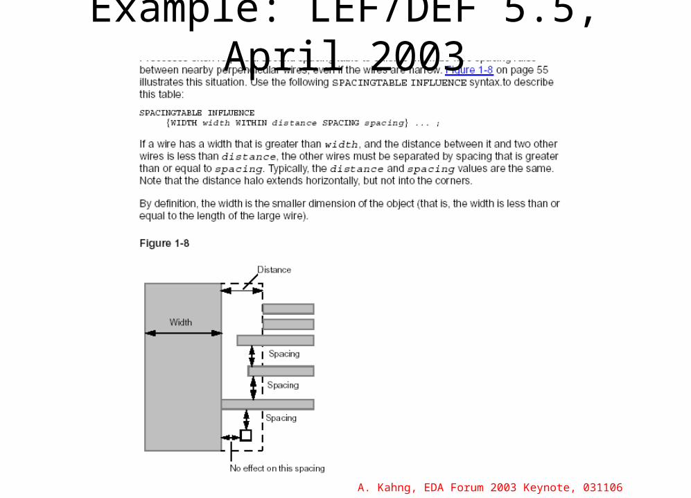
Example: LEF/DEF 5.5, April 2003
A. Kahng, EDA Forum 2003 Keynote, 031106
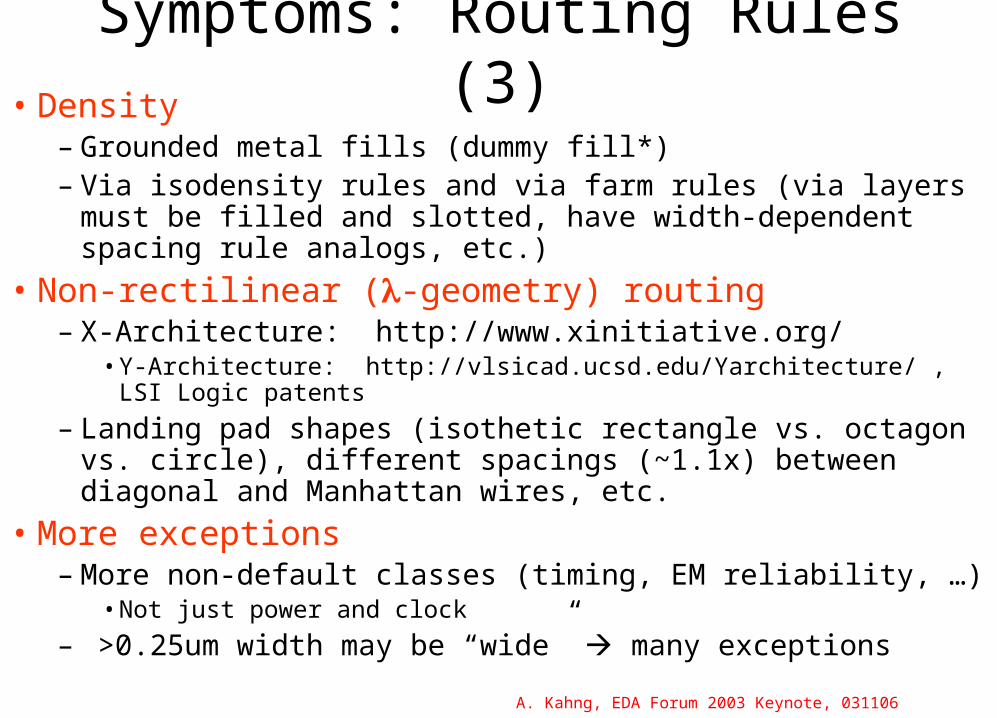
• Density– Grounded metal fills (dummy fill*)– Via isodensity rules and via farm rules (via layers must be filled
and slotted, have width-dependent spacing rule analogs, etc.)
• Non-rectilinear (-geometry) routing– X-Architecture: http://www.xinitiative.org/
• Y-Architecture: http://vlsicad.ucsd.edu/Yarchitecture/ , LSI Logic patents
– Landing pad shapes (isothetic rectangle vs. octagon vs. circle), different spacings (~1.1x) between diagonal and Manhattan wires, etc.
• More exceptions– More non-default classes (timing, EM reliability, …)
• Not just power and clock
– >0.25um width may be “wide” many exceptions
Symptoms: Routing Rules (3)
A. Kahng, EDA Forum 2003 Keynote, 031106
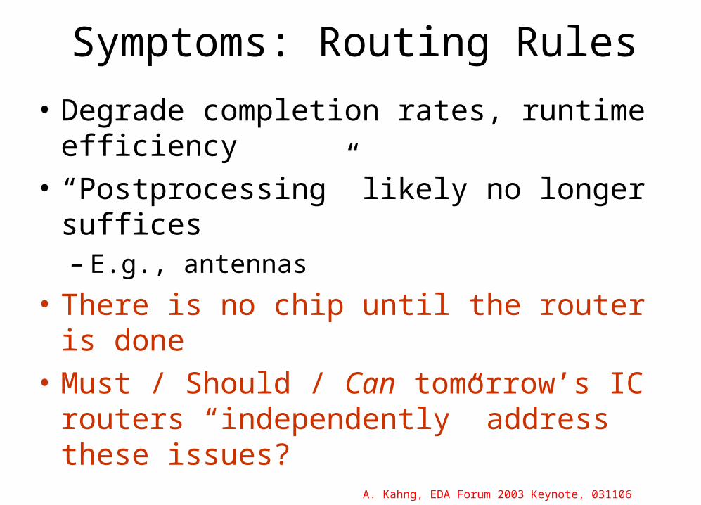
Symptoms: Routing Rules
• Degrade completion rates, runtime efficiency
• “Postprocessing” likely no longer suffices – E.g., antennas
• There is no chip until the router is done
• Must / Should / Can tomorrow’s IC routers “independently” address these issues?
A. Kahng, EDA Forum 2003 Keynote, 031106
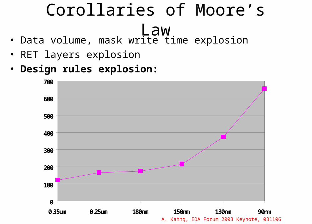
Corollaries of Moore’s Law
Number of design rules per process node
0
100
200
300
400
500
600
700
0.35um 0.25um 180nm 150nm 130nm 90nm
• Data volume, mask write time explosion• RET layers explosion• Design rules explosion:
A. Kahng, EDA Forum 2003 Keynote, 031106
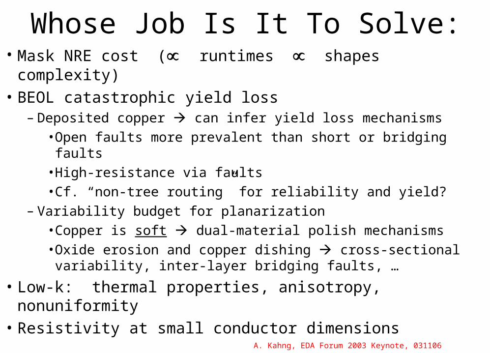
• Mask NRE cost ( runtimes shapes complexity)
• BEOL catastrophic yield loss– Deposited copper can infer yield loss mechanisms
• Open faults more prevalent than short or bridging faults• High-resistance via faults• Cf. “non-tree routing” for reliability and yield?
– Variability budget for planarization• Copper is soft dual-material polish mechanisms• Oxide erosion and copper dishing cross-sectional
variability, inter-layer bridging faults, …
• Low-k: thermal properties, anisotropy, nonuniformity• Resistivity at small conductor dimensions
Whose Job Is It To Solve:
A. Kahng, EDA Forum 2003 Keynote, 031106
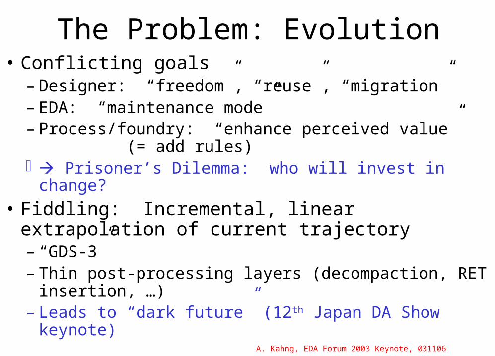
The Problem: Evolution• Conflicting goals
– Designer: “freedom”, “reuse”, “migration”– EDA: “maintenance mode”– Process/foundry: “enhance perceived value”
(= add rules) Prisoner’s Dilemma: who will invest in change?
• Fiddling: Incremental, linear extrapolation of current trajectory– “GDS-3”– Thin post-processing layers (decompaction, RET
insertion, …)– Leads to “dark future” (12th Japan DA Show keynote)
A. Kahng, EDA Forum 2003 Keynote, 031106
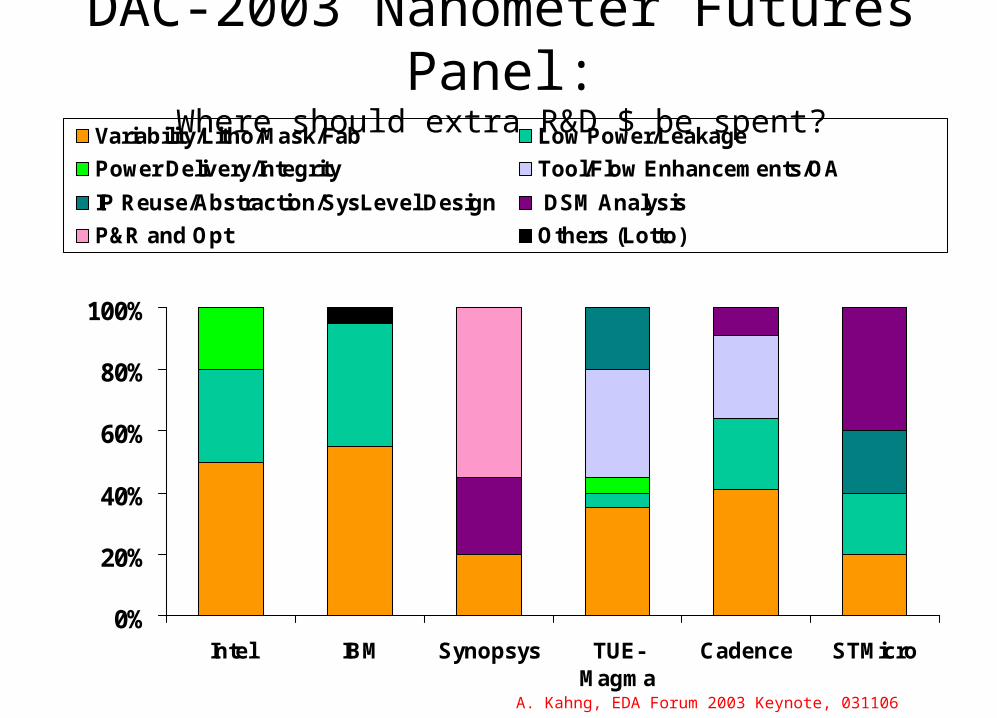
0%
20%
40%
60%
80%
100%
Intel IBM Synopsys TUE-Magma
Cadence STMicro
Variability/Litho/Mask/Fab Low Power/Leakage
Power Delivery/Integrity Tool/Flow Enhancements/OA
IP Reuse/Abstraction/SysLevel Design DSM Analysis
P&R and Opt Others (Lotto)
DAC-2003 Nanometer Futures Panel:Where should extra R&D $ be spent?
A. Kahng, EDA Forum 2003 Keynote, 031106
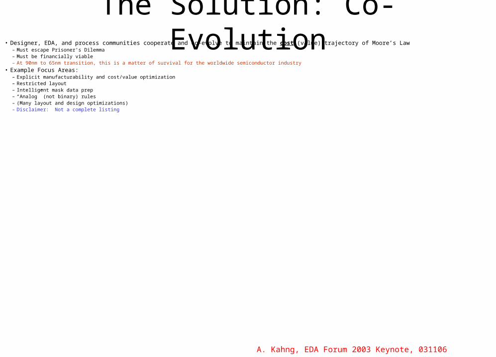
The Solution: Co-Evolution• Designer, EDA, and process communities cooperate and co-evolve to maintain the cost (value) trajectory of Moore’s Law
– Must escape Prisoner’s Dilemma– Must be financially viable– At 90nm to 65nm transition, this is a matter of survival for the worldwide semiconductor industry
• Example Focus Areas:– Explicit manufacturability and cost/value optimization– Restricted layout – Intelligent mask data prep– “Analog” (not binary) rules– (Many layout and design optimizations)– Disclaimer: Not a complete listing
A. Kahng, EDA Forum 2003 Keynote, 031106
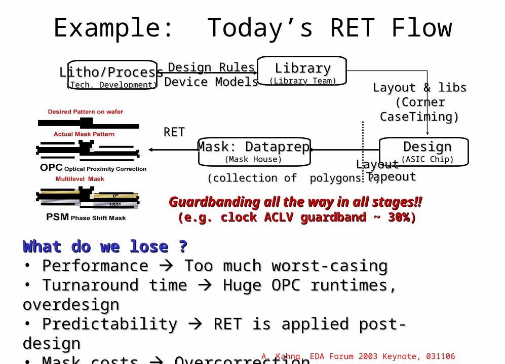
Example: Today’s RET Flow
Litho/ProcessLitho/Process(Tech. Development)(Tech. Development)
LibraryLibrary(Library Team)(Library Team)
Layout & libs Layout & libs (Corner (Corner
CaseTiming)CaseTiming)
DesignDesign(ASIC Chip)(ASIC Chip)
Mask: DataprepMask: Dataprep(Mask House)(Mask House)
Design RulesDesign RulesDevice ModelsDevice Models
TapeoutTapeout LayoutLayout
(collection of polygons ?)(collection of polygons ?)
RETRET
Guardbanding all the way in all stages!! Guardbanding all the way in all stages!! (e.g. clock ACLV guardband ~ 30%)(e.g. clock ACLV guardband ~ 30%)
What do we lose ?What do we lose ?• Performance Performance Too much worst-casing Too much worst-casing• Turnaround time Turnaround time Huge OPC runtimes, overdesign Huge OPC runtimes, overdesign• Predictability Predictability RET is applied post-design RET is applied post-design• Mask costs Mask costs Overcorrection Overcorrection• Designer’s intent Designer’s intent RET is not driven by design RET is not driven by design
A. Kahng, EDA Forum 2003 Keynote, 031106
• Bidirectional design-manufacturing data pipe– Fundamental drivers: cost, value
• Pass functional intent to manufacturing flow– Example: RET for predictable timing slack, leakage, yield
– RETs should win $$$, reduce performance variation
cost-driven, parametric yield constrained RET
• Pass limits of manufacturing flow up to design– Example: avoid corrections that cannot be manufactured or
verified e.g., design should be aware of metrology
N.B.: 1998-2003 papers/tutorials: http://vlsicad.ucsd.edu/~abk/TALKS/
Foundation of the DFM Solution
A. Kahng, EDA Forum 2003 Keynote, 031106
OutlineOutline
• The Design Roadmap
• DFM: Symptoms, Problem, Solution
• DFM Futures: Some Examples
A. Kahng, EDA Forum 2003 Keynote, 031106
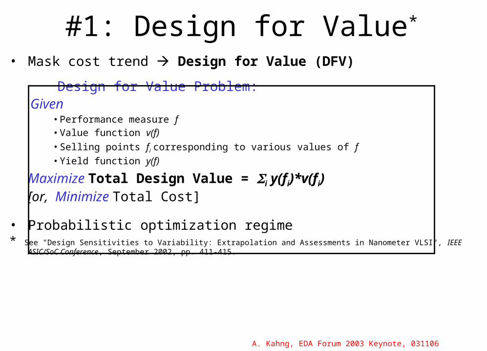
#1: Design for Value*
• Mask cost trend Design for Value (DFV)
Design for Value Problem: Given
• Performance measure f• Value function v(f)
• Selling points fi corresponding to various values of f
• Yield function y(f)
Maximize Total Design Value = i y(fi)*v(fi)[or, Minimize Total Cost]
• Probabilistic optimization regime* See "Design Sensitivities to Variability: Extrapolation and Assessments in Nanometer VLSI", IEEE ASIC/SoC Conference,
September 2002, pp. 411-415.
A. Kahng, EDA Forum 2003 Keynote, 031106
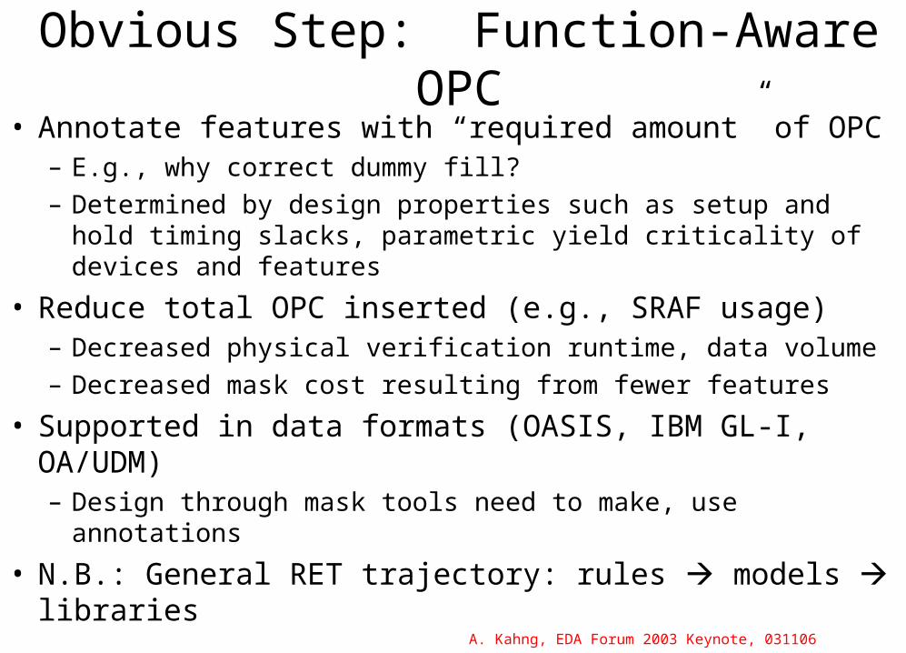
Obvious Step: Function-Aware OPC• Annotate features with “required amount” of OPC
– E.g., why correct dummy fill?– Determined by design properties such as setup and hold timing
slacks, parametric yield criticality of devices and features
• Reduce total OPC inserted (e.g., SRAF usage)– Decreased physical verification runtime, data volume– Decreased mask cost resulting from fewer features
• Supported in data formats (OASIS, IBM GL-I, OA/UDM)– Design through mask tools need to make, use annotations
• N.B.: General RET trajectory: rules models libraries
A. Kahng, EDA Forum 2003 Keynote, 031106
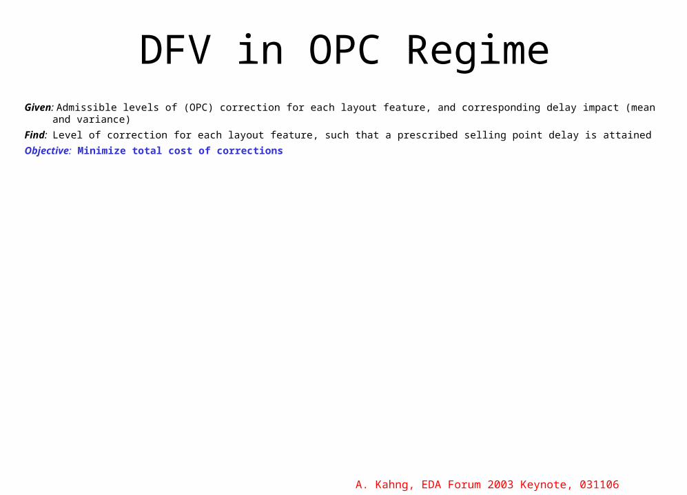
DFV in OPC RegimeGiven: Admissible levels of (OPC) correction for each layout feature, and corresponding delay impact (mean and variance)
Find: Level of correction for each layout feature, such that a prescribed selling point delay is attained
Objective: Minimize total cost of corrections
A. Kahng, EDA Forum 2003 Keynote, 031106
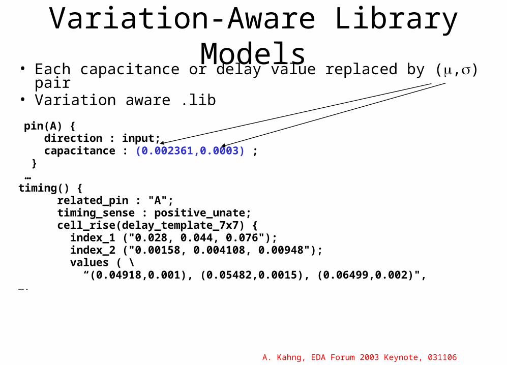
Variation-Aware Library Models• Each capacitance or delay value replaced by (,) pair• Variation aware .lib
pin(A) { direction : input; capacitance : (0.002361,0.0003) ; } …timing() { related_pin : "A"; timing_sense : positive_unate; cell_rise(delay_template_7x7) { index_1 ("0.028, 0.044, 0.076"); index_2 ("0.00158, 0.004108, 0.00948"); values ( \ “(0.04918,0.001), (0.05482,0.0015), (0.06499,0.002)", ….
A. Kahng, EDA Forum 2003 Keynote, 031106
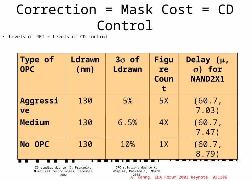
Correction = Mask Cost = CD Control
• Levels of RET = levels of CD control
OPC solutions due to K. Wampler, MaskTools, March 2003
CD studies due to D. Pramanik, Numerical Technologies, December 2002
Type of OPC
Ldrawn (nm)
3 of Ldrawn
Figure Count
Delay (, ) for NAND2X1
Aggressive 130 5% 5X (60.7, 7.03)
Medium 130 6.5% 4X (60.7, 7.47)
No OPC 130 10% 1X (60.7, 8.79)
• Levels of RET = Levels of CD control
A. Kahng, EDA Forum 2003 Keynote, 031106
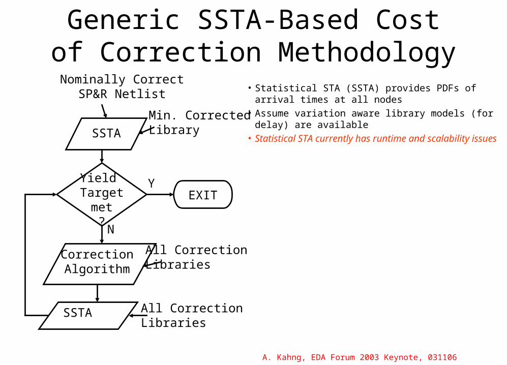
Generic SSTA-Based Cost of Correction Methodology
• Statistical STA (SSTA) provides PDFs of arrival times at all nodes
• Assume variation aware library models (for delay) are available
• Statistical STA currently has runtime and scalability issuesSSTA
Nominally Correct SP&R Netlist
Min. CorrectedLibrary
Yield Target met
?EXIT
CorrectionAlgorithm
SSTA
All CorrectionLibraries
All CorrectionLibraries
Y
N
A. Kahng, EDA Forum 2003 Keynote, 031106
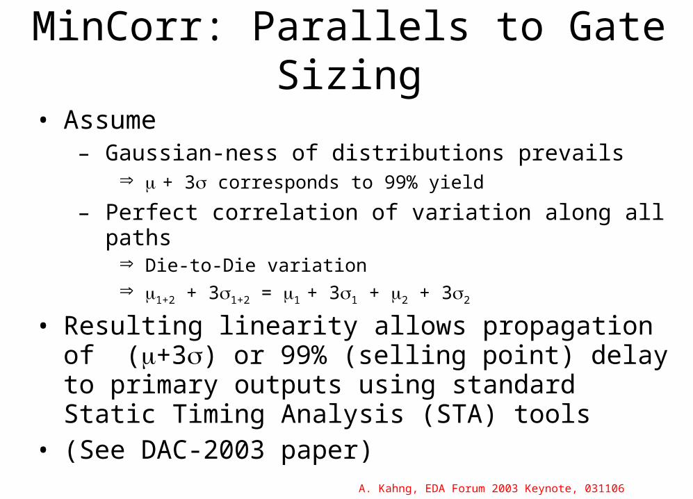
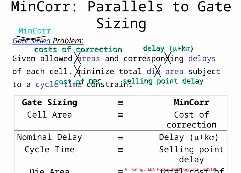
MinCorr: Parallels to Gate Sizing
• Assume– Gaussian-ness of distributions prevails
+ 3 corresponds to 99% yield
– Perfect correlation of variation along all paths Die-to-Die variation 1+2 + 31+2 = 1 + 31 + 2 + 32
• Resulting linearity allows propagation of (+3) or 99% (selling point) delay to primary outputs using standard Static Timing Analysis (STA) tools
• (See DAC-2003 paper)
A. Kahng, EDA Forum 2003 Keynote, 031106
MinCorr: Parallels to Gate Sizing
Gate Sizing MinCorr
Cell Area Cost of correction
Nominal Delay Delay (+k)
Cycle Time Selling point delay
Die Area Total cost of OPC
Gate Sizing Problem:
Given allowed areas and corresponding delays of each cell,
minimize total die area subject to a cycle time constraint
costs of correctioncosts of correction delay (delay (+k+k))
cost of OPCcost of OPC selling point delayselling point delay
MinCorr
A. Kahng, EDA Forum 2003 Keynote, 031106
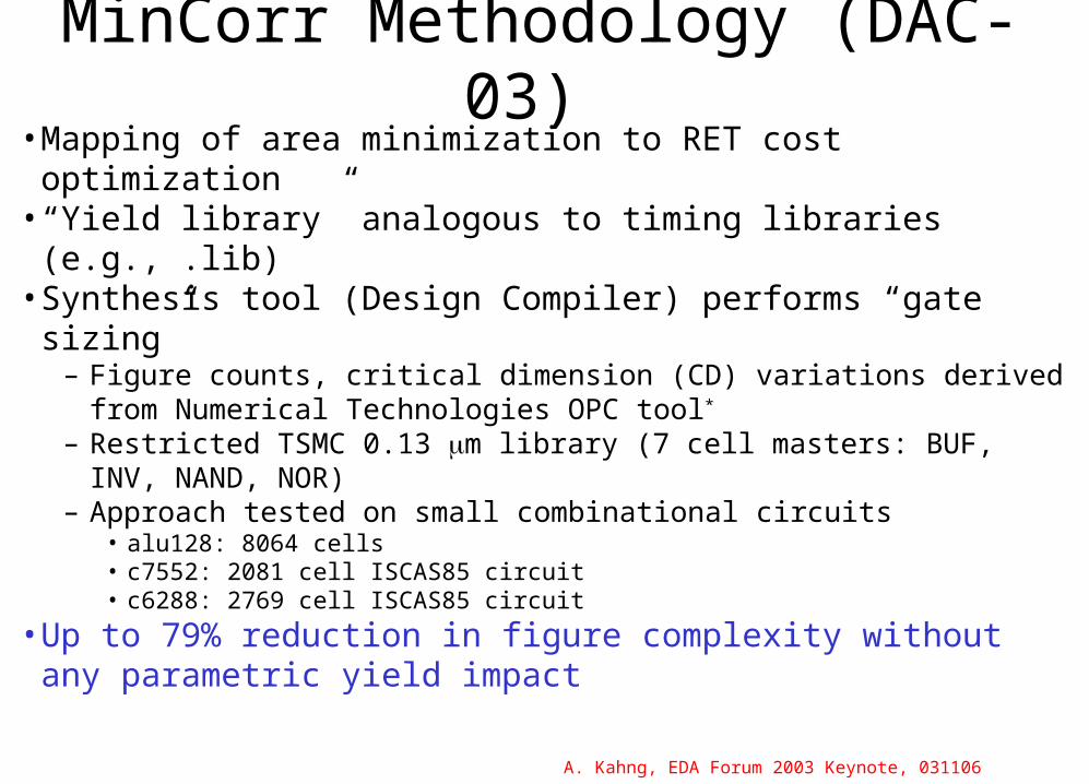
• Mapping of area minimization to RET cost optimization• “Yield library” analogous to timing libraries (e.g., .lib)• Synthesis tool (Design Compiler) performs “gate sizing”
– Figure counts, critical dimension (CD) variations derived from Numerical Technologies OPC tool*
– Restricted TSMC 0.13 m library (7 cell masters: BUF, INV, NAND, NOR)
– Approach tested on small combinational circuits • alu128: 8064 cells• c7552: 2081 cell ISCAS85 circuit• c6288: 2769 cell ISCAS85 circuit
• Up to 79% reduction in figure complexity without any parametric yield impact
MinCorr Methodology (DAC-03)
A. Kahng, EDA Forum 2003 Keynote, 031106
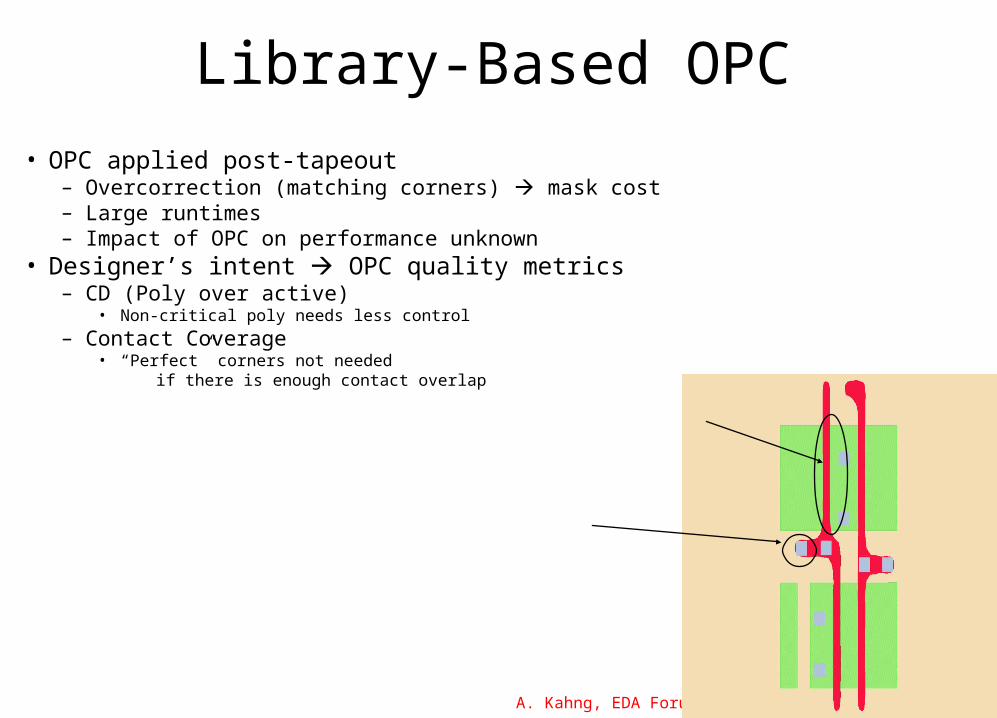
Library-Based OPC
• OPC applied post-tapeout – Overcorrection (matching corners) mask cost– Large runtimes – Impact of OPC on performance unknown
• Designer’s intent OPC quality metrics– CD (Poly over active)
• Non-critical poly needs less control
– Contact Coverage• “Perfect” corners not needed if there is enough contact overlap
A. Kahng, EDA Forum 2003 Keynote, 031106
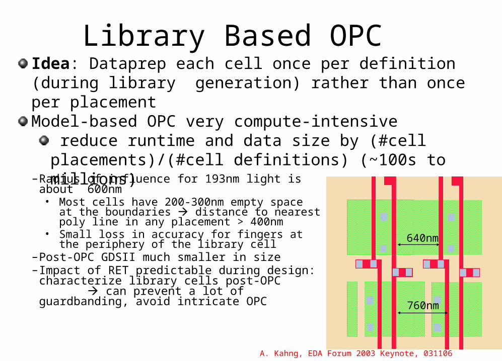
Library Based OPC
–Radius of influence for 193nm light is about 600nm• Most cells have 200-300nm empty space at
the boundaries distance to nearest poly line in any placement > 400nm
• Small loss in accuracy for fingers at the periphery of the library cell
–Post-OPC GDSII much smaller in size– Impact of RET predictable during design:
characterize library cells post-OPC can prevent a lot of guardbanding, avoid intricate OPC
Idea: Dataprep each cell once per definition (during library generation) rather than once per placementModel-based OPC very compute-intensive
reduce runtime and data size by (#cell placements)/(#cell definitions) (~100s to millions)
640nm
760nm
A. Kahng, EDA Forum 2003 Keynote, 031106
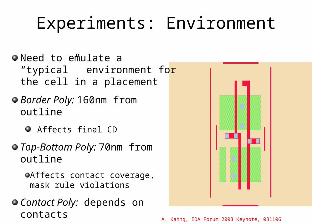
Experiments: Environment
Need to emulate a “typical” environment for the cell in a placement
Border Poly: 160nm from outline
Affects final CD
Top-Bottom Poly: 70nm from outline
Affects contact coverage, mask rule violations
Contact Poly: depends on contacts
Affects contact coverage, mask rule violations
A. Kahng, EDA Forum 2003 Keynote, 031106
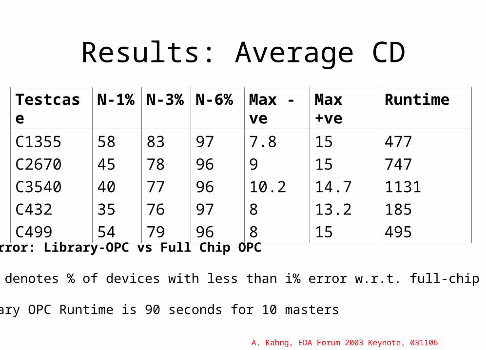
Results: Average CD
CD error: Library-OPC vs Full Chip OPC
N-i% denotes % of devices with less than i% error w.r.t. full-chip OPC
Library OPC Runtime is 90 seconds for 10 masters
Testcase N-1% N-3% N-6% Max -ve Max +ve Runtime
C1355
C2670
C3540
C432
C499
58
45
40
35
54
83
78
77
76
79
97
96
96
97
96
7.8
9
10.2
8
8
15
15
14.7
13.2
15
477
747
1131
185
495
A. Kahng, EDA Forum 2003 Keynote, 031106
#2: Process-Aware Design• Anisotropy in H vs. V bias
– Features in one direction (scanning, raster write, …) may be better controllable than those in the orthogonal direction
– Single orientation throughout layout is preferred– Dominant (critical-feature) orientation in layout design should
match write direction
• Wafer symmetries (e.g., etch gradient due to spin-on)• Iso-Dense balancing (imaging through focus)
A. Kahng, EDA Forum 2003 Keynote, 031106
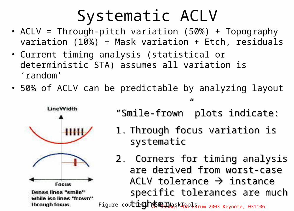
Systematic ACLV• ACLV = Through-pitch variation (50%) + Topography
variation (10%) + Mask variation + Etch, residuals• Current timing analysis (statistical or deterministic
STA) assumes all variation is ‘random’• 50% of ACLV can be predictable by analyzing layout
““Smile-frown” plots indicate: Smile-frown” plots indicate:
1.1. Through focus variation is systematicThrough focus variation is systematic
2.2. Corners for timing analysis are Corners for timing analysis are derived from worst-case ACLV derived from worst-case ACLV tolerance tolerance instance specific instance specific tolerances are much tightertolerances are much tighter
Figure courtesy ASML MaskTools
A. Kahng, EDA Forum 2003 Keynote, 031106
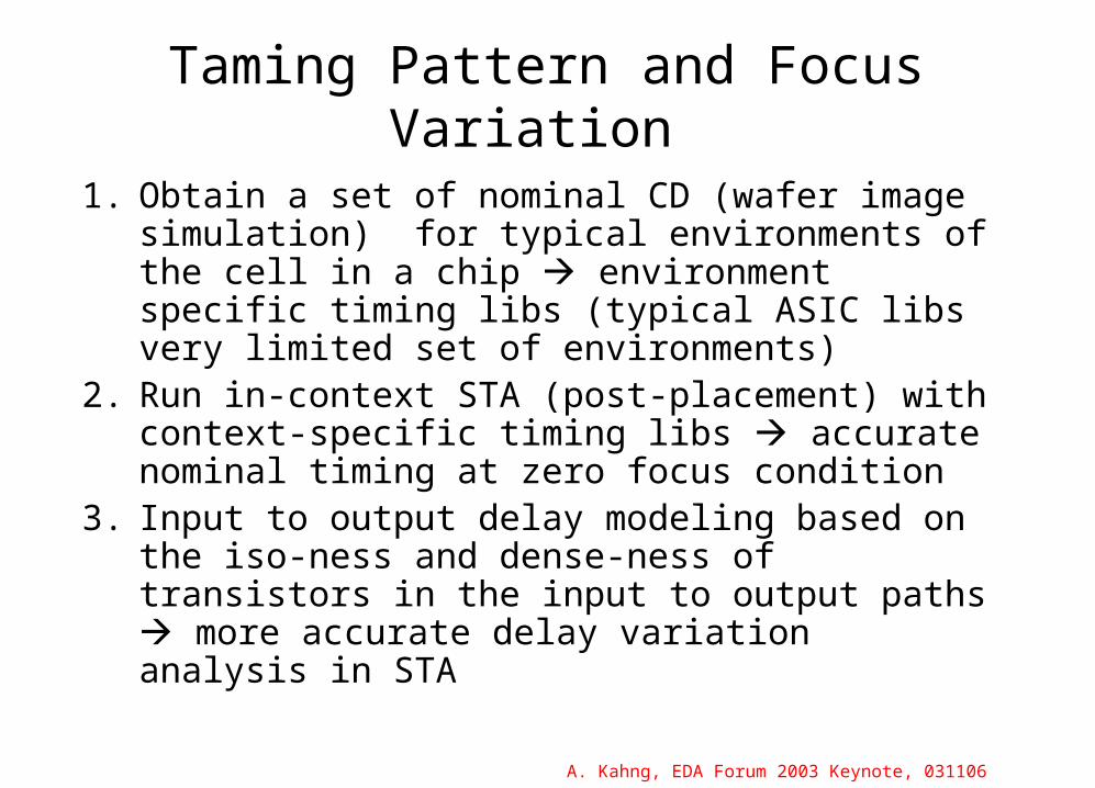
Taming Pattern and Focus Variation
1. Obtain a set of nominal CD (wafer image simulation) for typical environments of the cell in a chip environment specific timing libs (typical ASIC libs very limited set of environments)
2. Run in-context STA (post-placement) with context-specific timing libs accurate nominal timing at zero focus condition
3. Input to output delay modeling based on the iso-ness and dense-ness of transistors in the input to output paths more accurate delay variation analysis in STA
A. Kahng, EDA Forum 2003 Keynote, 031106
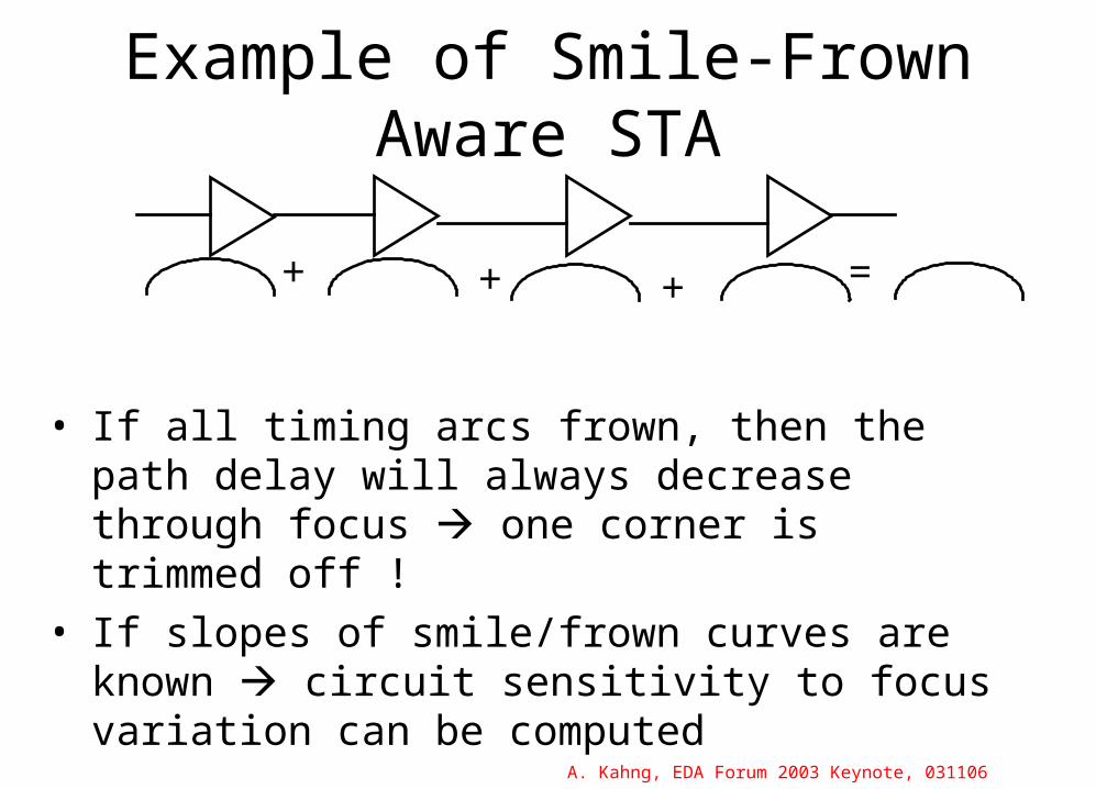
Example of Smile-Frown Aware STA
• If all timing arcs frown, then the path delay will always decrease through focus one corner is trimmed off !
• If slopes of smile/frown curves are known circuit sensitivity to focus variation can be computed
+ ++ =
A. Kahng, EDA Forum 2003 Keynote, 031106
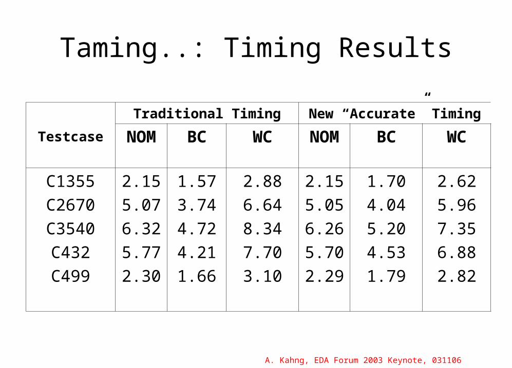
Taming..: Timing Results
Testcase
Traditional Timing New “Accurate” Timing
NOM BC WC NOM BC WC
C1355
C2670
C3540
C432
C499
2.15
5.07
6.32
5.77
2.30
1.57
3.74
4.72
4.21
1.66
2.88
6.64
8.34
7.70
3.10
2.15
5.05
6.26
5.70
2.29
1.70
4.04
5.20
4.53
1.79
2.62
5.96
7.35
6.88
2.82
A. Kahng, EDA Forum 2003 Keynote, 031106
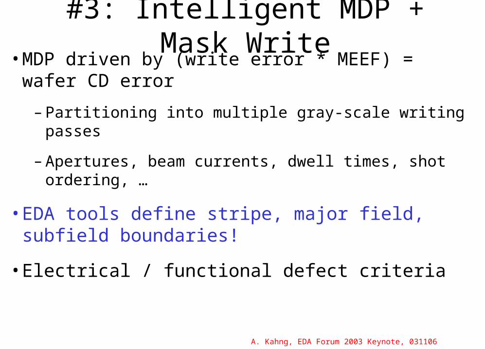
#3: Intelligent MDP + Mask Write• MDP driven by (write error * MEEF) = wafer CD error
– Partitioning into multiple gray-scale writing passes
– Apertures, beam currents, dwell times, shot ordering, …
• EDA tools define stripe, major field, subfield boundaries!
• Electrical / functional defect criteria
A. Kahng, EDA Forum 2003 Keynote, 031106
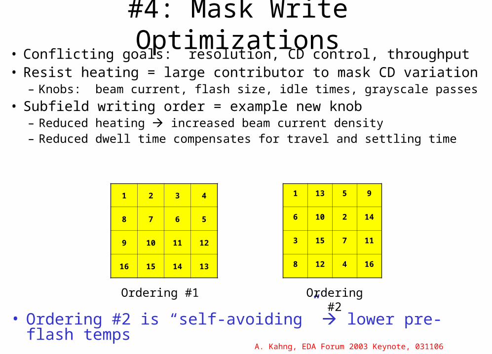
#4: Mask Write Optimizations• Conflicting goals: resolution, CD control, throughput• Resist heating = large contributor to mask CD variation
– Knobs: beam current, flash size, idle times, grayscale passes
• Subfield writing order = example new knob– Reduced heating increased beam current density– Reduced dwell time compensates for travel and settling time
• Ordering #2 is “self-avoiding” lower pre-flash temps
1 2 3 4
8 7 6 5
9 10 11 12
16 15 14 13
Ordering #1
1 13 5 9
6 10 2 14
3 15 7 11
8 12 4 16
Ordering #2
A. Kahng, EDA Forum 2003 Keynote, 031106
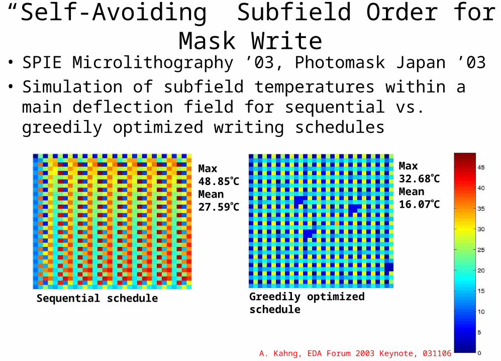
• SPIE Microlithography ’03, Photomask Japan ’03• Simulation of subfield temperatures within a main
deflection field for sequential vs. greedily optimized writing schedules
Max48.85CMean27.59C
Sequential schedule
Max32.68CMean16.07C
Greedily optimized schedule
“Self-Avoiding” Subfield Order for Mask Write
A. Kahng, EDA Forum 2003 Keynote, 031106
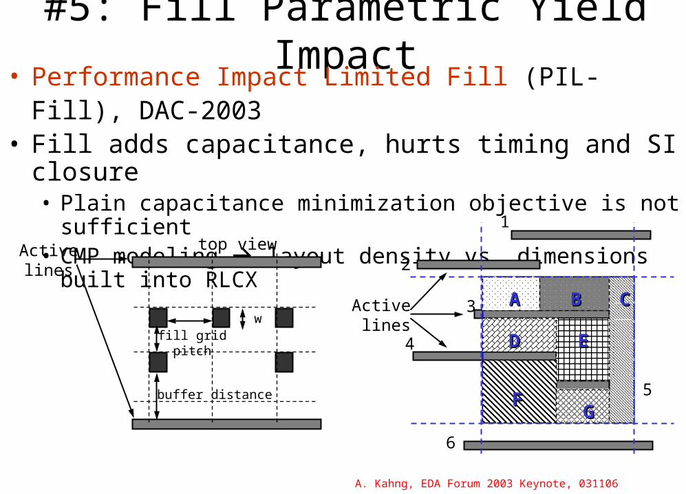
#5: Fill Parametric Yield Impact• Performance Impact Limited Fill (PIL-Fill), DAC-2003• Fill adds capacitance, hurts timing and SI closure
• Plain capacitance minimization objective is not sufficient• CMP modeling layout density vs. dimensions built into RLCX
top view
buffer distance
fill gridpitch
Activelines
wBBAA CC
DD EE
GGFF
1
2
3
4
6
5
Activelines
A. Kahng, EDA Forum 2003 Keynote, 031106
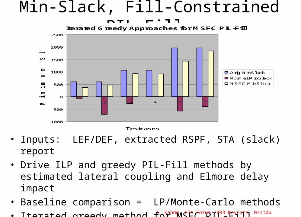
Min-Slack, Fill-Constrained PIL-Fill
• Inputs: LEF/DEF, extracted RSPF, STA (slack) report• Drive ILP and greedy PIL-Fill methods by estimated lateral
coupling and Elmore delay impact• Baseline comparison = LP/Monte-Carlo methods• Iterated greedy method for MSFC PIL-Fill reduces timing slack
impact of fill by 80% (average over all nets), 63% (worst net)
Iterated Greedy Approaches for MSFC PIL-Fill
-1000
-500
0
500
1000
1500
2000
2500
1 2 3 4 5 6
Testcases
M i n
i m
u m
S
l a
c k
(p
s)
Orig MinSlack
Normal MinSlack
MSFC MinSlack
A. Kahng, EDA Forum 2003 Keynote, 031106
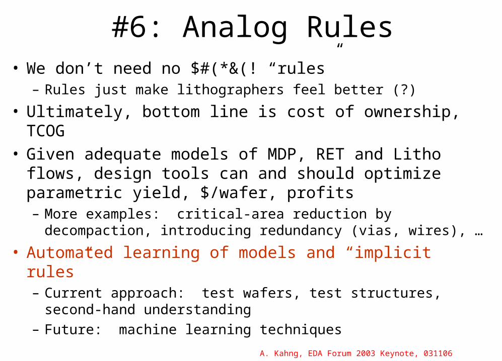
#6: Analog Rules• We don’t need no $#(*&(! “rules”
– Rules just make lithographers feel better (?)
• Ultimately, bottom line is cost of ownership, TCOG• Given adequate models of MDP, RET and Litho flows,
design tools can and should optimize parametric yield, $/wafer, profits– More examples: critical-area reduction by decompaction,
introducing redundancy (vias, wires), …
• Automated learning of models and “implicit rules”– Current approach: test wafers, test structures, second-hand
understanding– Future: machine learning techniques
A. Kahng, EDA Forum 2003 Keynote, 031106
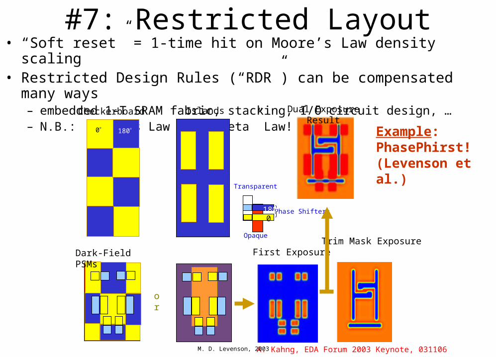
#7: Restricted Layout• “Soft reset” = 1-time hit on Moore’s Law density scaling• Restricted Design Rules (“RDR”) can be compensated many ways
– embedded 1-T SRAM fabric, stacking, I/O circuit design, …– N.B.: Moore’s Law is a “meta” Law!
Opaque
Phase Shifters0
180
Transparent
Checkerboard Islands
First ExposureTrim Mask Exposure
Dual Exposure Result
Dark-Field PSMs
or
0
180 Example: PhasePhirst! (Levenson et al.)
M. D. Levenson, 2003
A. Kahng, EDA Forum 2003 Keynote, 031106
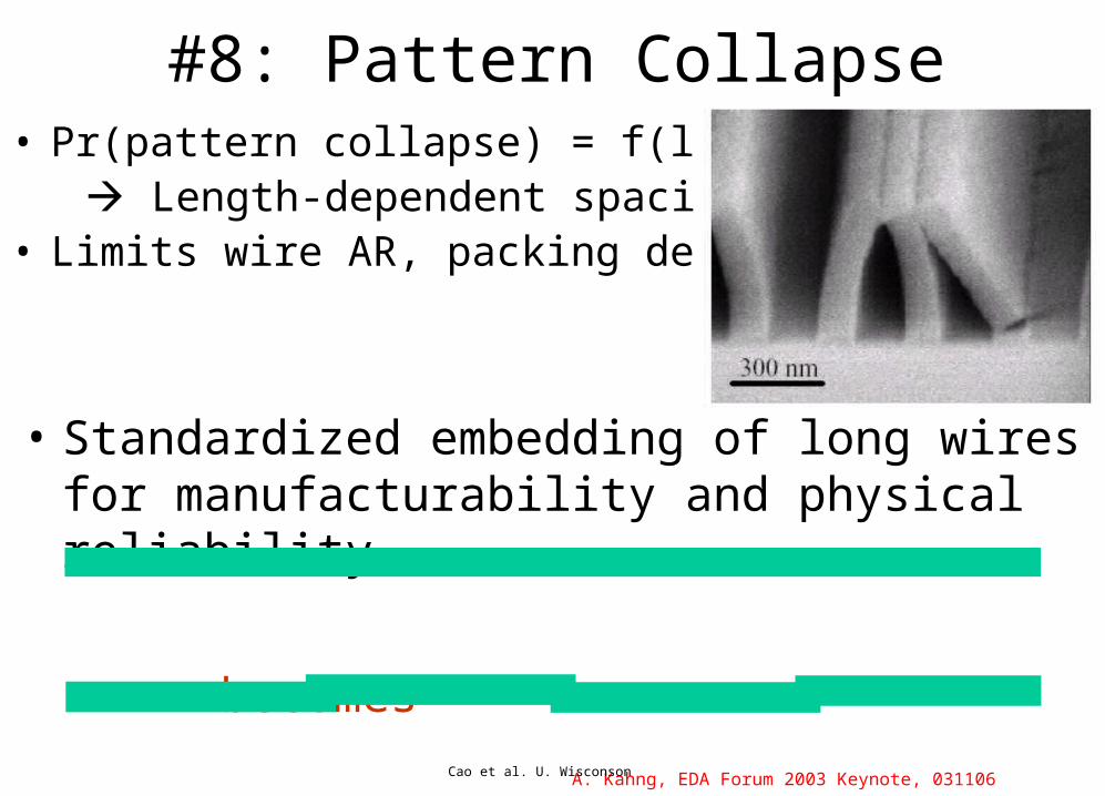
#8: Pattern Collapse• Pr(pattern collapse) = f(length) Length-dependent spacing rules• Limits wire AR, packing density
Cao et al. U. Wisconson
• Standardized embedding of long wires for manufacturability and physical reliability
becomes
???
A. Kahng, EDA Forum 2003 Keynote, 031106
#9: Data Compression• Today: RET + complexity exploding data volume
• Partitioning of compression and decompression?– Equipment architecture question – where to put engines, I/F’s, storage?
– Largely orthogonal to design considerations
– Procedural compression largely unexplored? (Ex: Verilog + SP&R binaries + runscripts = representation of detail-routed layout)
• Design for compressibility? (DATE ’03, SPIE ML ’03)– What is ROI of relaxing constraints on layout? Of +k bytes of data?
– How context-sensitive must patterning be? (Lessons from RET…)
• Use of lossy compression? (SPIE ML ’03)– What design features can be “lost”? (Ex: dummy fill)
A. Kahng, EDA Forum 2003 Keynote, 031106
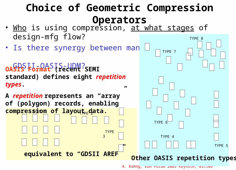
Choice of Geometric Compression Operators• Who is using compression, at what stages of design-mfg flow?
• Is there synergy between manufacturing flow and GDSII-OASIS-UDM?
TYPE 1 TYPE 2
TYPE 3
equivalent to “GDSII AREF”
TYPE 4
TYPE 5
TYPE 6
TYPE 7
TYPE 8
Other OASIS repetition types
OASIS Format (recent SEMI standard) defines eight repetition types.
A repetition represents an “array” of (polygon) records, enabling compression of layout data.
A. Kahng, EDA Forum 2003 Keynote, 031106
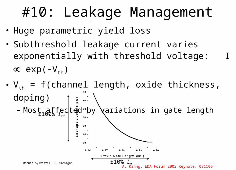
#10: Leakage Management• Huge parametric yield loss
• Subthreshold leakage current varies exponentially with
threshold voltage: I exp(-Vth)
• Vth = f(channel length, oxide thickness, doping)
– Most affected by variations in gate length
±10% Ld
±100% Isub
Dennis Sylvester, U. Michigan
A. Kahng, EDA Forum 2003 Keynote, 031106
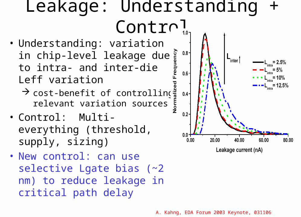
Leakage: Understanding + Control
• Understanding: variation in chip-level leakage due to intra- and inter-die Leff variation cost-benefit of controlling
relevant variation sources
• Control: Multi-everything (threshold, supply, sizing)
• New control: can use selective Lgate bias (~2 nm) to reduce leakage in critical path delay
A. Kahng, EDA Forum 2003 Keynote, 031106
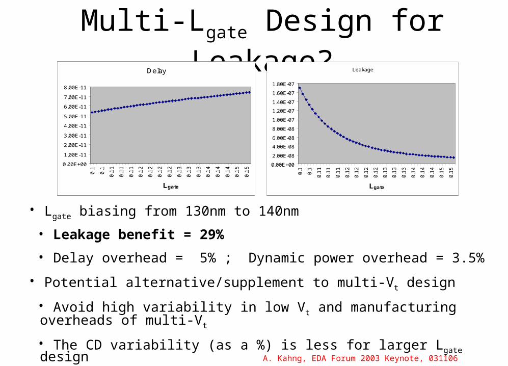
Multi-Lgate Design for Leakage?
• Lgate biasing from 130nm to 140nm
• Leakage benefit = 29%
• Delay overhead = 5% ; Dynamic power overhead = 3.5%
• Potential alternative/supplement to multi-Vt design
• Avoid high variability in low Vt and manufacturing overheads of multi-Vt
• The CD variability (as a %) is less for larger Lgate design
Delay
0.00E+00
1.00E-11
2.00E-11
3.00E-11
4.00E-11
5.00E-11
6.00E-11
7.00E-11
8.00E-110
.1
0.1
0.1
1
0.1
1
0.1
1
0.1
2
0.1
2
0.1
2
0.1
2
0.1
3
0.1
3
0.1
3
0.1
4
0.1
4
0.1
4
0.1
5
0.1
5
Lgate
Leakage
0.00E+00
2.00E-08
4.00E-08
6.00E-08
8.00E-08
1.00E-07
1.20E-07
1.40E-07
1.60E-07
1.80E-07
0.1
0.1
0.1
1
0.1
1
0.1
1
0.1
2
0.1
2
0.1
2
0.1
2
0.1
3
0.1
3
0.1
3
0.1
4
0.1
4
0.1
4
0.1
5
0.1
5
Lgate
A. Kahng, EDA Forum 2003 Keynote, 031106
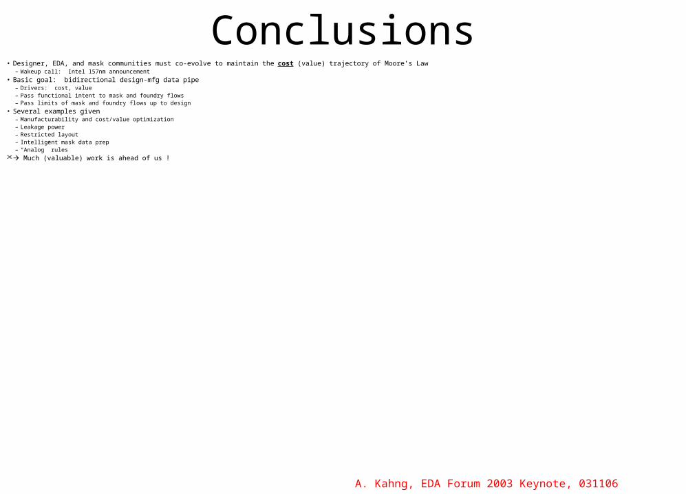
Conclusions• Designer, EDA, and mask communities must co-evolve to maintain the cost (value) trajectory of Moore’s Law
– Wakeup call: Intel 157nm announcement
• Basic goal: bidirectional design-mfg data pipe– Drivers: cost, value– Pass functional intent to mask and foundry flows– Pass limits of mask and foundry flows up to design
• Several examples given– Manufacturability and cost/value optimization– Leakage power– Restricted layout – Intelligent mask data prep– “Analog” rules
Much (valuable) work is ahead of us !
A. Kahng, EDA Forum 2003 Keynote, 031106
THANK YOU !


