Information furnished by Analog Devices is believed to be accurate andreliable. However, no responsibility is assumed by Analog Devices for itsuse, nor for any infringements of patents or other rights of third partieswhich may result from its use. No license is granted by implication orotherwise under any patent or patent rights of Analog Devices.
aAD8036/AD8037
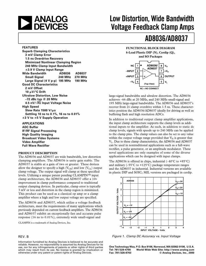
large-signal bandwidths and ultralow distortion. The AD8036achieves –66 dBc at 20 MHz, and 240 MHz small-signal and195 MHz large-signal bandwidths. The AD8036 and AD8037’srecover from 2× clamp overdrive within 1.5 ns. These character-istics position the AD8036/AD8037 ideally for driving as well asbuffering flash and high resolution ADCs.
In addition to traditional output clamp amplifier applications,the input clamp architecture supports the clamp levels as addi-tional inputs to the amplifier. As such, in addition to static dcclamp levels, signals with speeds up to 240 MHz can be appliedto the clamp pins. The clamp values can also be set to any valuewithin the output voltage range provided that VH is greater thatVL. Due to these clamp characteristics, the AD8036 and AD8037can be used in nontraditional applications such as a full-waverectifier, a pulse generator, or an amplitude modulator. Thesenovel applications are only examples of some of the diverseapplications which can be designed with input clamps.
The AD8036 is offered in chips, industrial (–40°C to +85°C)and military (–55°C to +125°C) package temperature rangesand the AD8037 in industrial. Industrial versions are availablein plastic DIP and SOIC; MIL versions are packaged in cerdip.
PRODUCT DESCRIPTIONThe AD8036 and AD8037 are wide bandwidth, low distortionclamping amplifiers. The AD8036 is unity gain stable. TheAD8037 is stable at a gain of two or greater. These devicesallow the designer to specify a high (VCH) and low (VCL) outputclamp voltage. The output signal will clamp at these specifiedlevels. Utilizing a unique patent pending CLAMPIN™ inputclamp architecture, the AD8036 and AD8037 offer a 10×improvement in clamp performance compared to traditionaloutput clamping devices. In particular, clamp error is typically3 mV or less and distortion in the clamp region is minimized.This product can be used as a classical op amp or a clampamplifier where a high and low output voltage are specified.
The AD8036 and AD8037, which utilize a voltage feedbackarchitecture, meet the requirements of many applications whichpreviously depended on current feedback amplifiers. The AD8036and AD8037 exhibit an exceptionally fast and accurate pulseresponse (16 ns to 0.01%), extremely wide small-signal and
CLAMPIN is a trademark of Analog Devices, Inc.
One Technology Way, P.O. Box 9106, Norwood, MA 02062-9106, U.S.A.
Tel: 781/329-4700 World Wide Web Site: http://www.analog.com
TMIN–TMAX 5 5 µACommon-Mode Rejection Ratio VCM = ±2 V 66 90 70 90 dBOpen-Loop Gain VOUT = ± 2.5 V 48 55 54 60 dB
TMIN–TMAX 40 46 dB
INPUT CHARACTERISTICSInput Resistance 500 500 kΩInput Capacitance 1.2 1.2 pFInput Common-Mode Voltage Range ± 2.5 ± 2.5 V
OUTPUT CHARACTERISTICSOutput Voltage Range, RL = 150 Ω ± 3.2 ± 3.9 ± 3.2 ± 3.9 VOutput Current 70 70 mAOutput Resistance 0.3 0.3 ΩShort Circuit Current 240 240 mA
POWER SUPPLYOperating Range ± 3.0 ± 5.0 ± 6.0 ± 3.0 ± 5.0 ± 6.0 VQuiescent Current 20.5 21.5 18.5 19.5 mA
TMIN–TMAX 25 24 mAPower Supply Rejection Ratio TMIN–TMAX 50 60 56 66 dB
NOTES1See Max Ratings and Theory of Operation sections of data sheet.2See Max Ratings.3Nonlinearity is defined as the voltage delta between the set input clamp voltage (VH or VL) and the voltage at which VOUT starts deviating from VIN (see Figure 73).4Measured at AV = 50.5Measured with respect to the inverting input.
. . . . . . . . . . . . . . . . . . . . . . Observe Power Derating CurvesStorage Temperature Range N, R . . . . . . . . . –65°C to +125°COperating Temperature Range (A Grade) . . . –40°C to +85°CLead Temperature Range (Soldering 10 sec) . . . . . . . . . 300°CNOTES1Stresses above those listed under Absolute Maximum Ratings may cause perma-nent damage to the device. This is a stress rating only; functional operation of thedevice at these or any other conditions above those indicated in the operationalsection of this specification is not implied. Exposure to absolute maximum ratingconditions for extended periods may affect device reliability.
2Specification is for device in free air:8-Lead Plastic DIP: θJA = 90°C/W8-Lead SOIC: θJA = 155°C/W8-Lead Cerdip: θJA = 110°C/W.
MAXIMUM POWER DISSIPATIONThe maximum power that can be safely dissipated by thesedevices is limited by the associated rise in junction temperature.The maximum safe junction temperature for plastic encapsulateddevices is determined by the glass transition temperature of theplastic, approximately 150°C. Exceeding this limit temporarilymay cause a shift in parametric performance due to a changein the stresses exerted on the die by the package. Exceedinga junction temperature of 175°C for an extended period canresult in device failure.
While the AD8036 and AD8037 are internally short circuit pro-tected, this may not be sufficient to guarantee that the maxi-mum junction temperature (150°C) is not exceeded under allconditions. To ensure proper operation, it is necessary to observethe maximum power derating curves.
2.0
0–50 80
1.5
0.5
–40
1.0
0 10–10–20–30 20 30 40 50 60 70 90AMBIENT TEMPERATURE – C
MA
XIM
UM
PO
WE
R D
ISS
IPA
TIO
N –
Wat
ts
TJ = +150C8-LEAD PLASTIC DIPPACKAGE
8-LEAD SOICPACKAGE
Figure 2. Plot of Maximum Power Dissipation vs. Temperature
METALIZATION PHOTODimensions shown in inches and (mm).
Connect Substrate to –VS.
AD8036
8036
AD8037
8037
+IN –VS
OUT
–IN +VSVH
VL
+IN –VS
OUT
–IN +VSVH
VL
4 53
2 8 7
2 8 7
6
6
3 4 5
0.050 (1.27)
0.046(1.17)
0.050 (1.27)
0.046(1.17)
ORDERING GUIDE
Temperature Package PackageModel Range Description Option
AD8036AN –40°C to +85°C Plastic DIP N-8AD8036AR –40°C to +85°C SOIC SO-8AD8036AR-REEL –40°C to +85°C 13" Tape and Reel SO-8AD8036AR-REEL7 –40°C to +85°C 7" Tape and Reel SO-8AD8036ACHIPS –40°C to +85°C DieAD8036-EB Evaluation Board5962-9559701MPA –55°C to +125°C Cerdip Q-8
AD8037AN –40°C to +85°C Plastic DIP N-8AD8037AR –40°C to +85°C SOIC SO-8AD8037AR-REEL –40°C to +85°C 13" Tape and Reel SO-8AD8037AR-REEL7 –40°C to +85°C 7" Tape and Reel SO-8AD8037ACHIPS –40°C to +85°C DieAD8037-EB Evaluation Board
CAUTIONESD (electrostatic discharge) sensitive device. Electrostatic charges as high as 4000 V readilyaccumulate on the human body and test equipment and can discharge without detection. Althoughthe AD8036/AD8037 features proprietary ESD protection circuitry, permanent damage may occuron devices subjected to high-energy electrostatic discharges. Therefore, proper ESD precautionsare recommended to avoid performance degradation or loss of functionality.
WARNING!
ESD SENSITIVE DEVICE
REV. B–4–
AD8036/AD8037
+VS
RL = 100
–VS
49.9
VIN
RF
130VOUT
0.1F
10F
AD8036
0.1F
10F
PULSEGENERATOR
TR/TF = 350ps
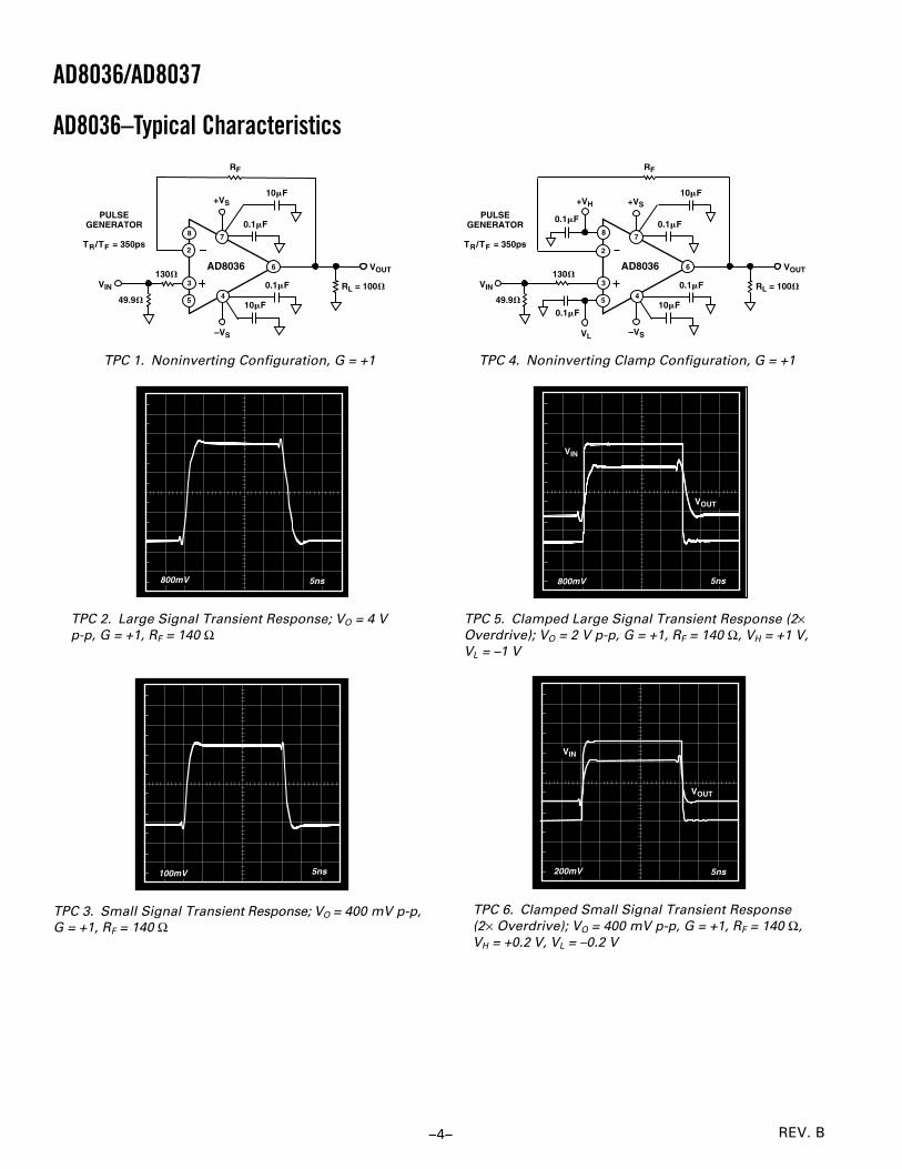
TPC 1. Noninverting Configuration, G = +1
TPC 2. Large Signal Transient Response; VO = 4 Vp-p, G = +1, RF = 140 Ω
TPC 3. Small Signal Transient Response; VO = 400 mV p-p,G = +1, RF = 140 Ω
AD8036–Typical Characteristics
+VS
RL = 100
–VS
49.9
VIN
RF
130VOUT
0.1F
10F
AD8036
0.1F
10F
PULSEGENERATOR
TR/TF = 350ps
+VH
VL
0.1F
0.1F
TPC 4. Noninverting Clamp Configuration, G = +1
TPC 5. Clamped Large Signal Transient Response (2×Overdrive); VO = 2 V p-p, G = +1, RF = 140 Ω, VH = +1 V,VL = –1 V
TPC 6. Clamped Small Signal Transient Response(2× Overdrive); VO = 400 mV p-p, G = +1, RF = 140 Ω,VH = +0.2 V, VL = –0.2 V
AD8036/AD8037
REV. B –5–
AD8037–Typical Characteristics
RIN
+VS
RL = 100
–VS
49.9
VIN
RF
100VOUT
0.1F
10F
AD8037
0.1F
10F
PULSEGENERATOR
TR/TF = 350ps
TPC 7. Noninverting Configuration, G = +2
TPC 8. Large Signal Transient Response; VO = 4 V p-p,G = +2, RF = RIN = 274 Ω
TPC 9. Small Signal Transient Response; VO = 400 mV p-p, G = +2, RF = RIN = 274 Ω
RIN
+VS
RL = 100
–VS
49.9
VIN
RF
100VOUT
0.1F
10F
AD8037
0.1F
10F
PULSEGENERATOR
TR/TF = 350ps
+VH
VL
0.1F
0.1F
TPC 10. Noninverting Clamp Configuration, G = +2
TPC 11. Clamped Large Signal Transient Response(2× Overdrive); VO = 2 V p-p, G = +2, RF = RIN = 274Ω, VH = +0.5 V, VL = –0.5 V
TPC 12. Clamped Small Signal Transient Response(2× Overdrive); VO = 400 mV p-p, G = +2, RF = RIN =274 Ω, VH = +0.1 V, VL = –0.1 V
REV. B–6–
AD8036/AD8037
AD8036–Typical Characteristics
200
140
GA
IN –
dB
102
49.9
1MFREQUENCY – Hz
10M 100M 1G
VO = 300mV p-p VS = 5V RL = 100
–8
–7
–6
–5
–4
–3
–2
–1
0
1
2
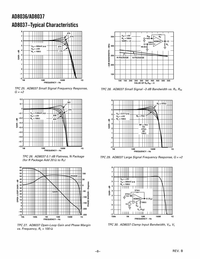
TPC 13. AD8036 Small Signal Frequency Response,G = +1
1M
158
140
150
10M 100M 1G
GA
IN –
dB
VO = 300mV p-p VS = 5V RL = 100
130
–0.8
–0.7
–0.6
–0.5
–0.4
–0.3
–0.2
–0.1
0
0.1
0.2
FREQUENCY – Hz
TPC 14. AD8036 0.1 dB Flatness, N Package (for RPackage Add 20 Ω to RF)
60
10
10k 100k 10M1M
30
20
40
50
FREQUENCY – Hz
OP
EN
-L
OO
P G
AIN
– d
B
0
–10
100M 1G
100
20
0
–20
40
60
80
–80
–100
–120
–60
–40
90
70
80
–20
PH
AS
E M
AR
GIN
– D
egre
es
GAIN
PHASE
TPC 15. AD8036 Open-Loop Gain and Phase Margin vs.Frequency, RL = 100 Ω
VALUE OF FEEDBACK RESISTOR (RF) –
–3d
B B
AN
DW
IDT
H –
MH
z
20 24040 200 2201801601401201008060
R PACKAGE
RF
130 AD8036
VS = 5VRL = 100
GAIN = +1RL
49.9 N PACKAGE
400
350
300
250
200
TPC 16. AD8036 Small Signal –3 dB Bandwidth vs. RF
OU
TP
UT
– d
B
1MFREQUENCY – Hz
10M 100M 1G
250
RF = 50
TO250
BY50
50
VS = 5V VO = 2.5V p-p RL = 100
–8
–7
–6
–5
–4
–3
–2
–1
0
1
2
TPC 17. AD8036 Large Signal Frequency Response,G = +1
FREQUENCY – Hz
GA
IN –
dB
1M 10M 100M 1G100k
VS = 5V VO = 300mV p-p RL = 100
–8
–7
–6
–5
–4
–3
–2
–1
0
1
2
140
VH
100
VL (VIN)
(VO)
1V
AD8036
TPC 18. AD8036 Clamp Input Bandwidth, VH, VL
AD8036/AD8037
REV. B –7–
–30
–130100k 100M10M1M10k
–70
–50
–110
–90
FREQUENCY – Hz
HA
RM
ON
IC D
IST
OR
TIO
N –
dB
c
VO = 2V p-p VS = 5V RL = 500
G = +1
2ND HARMONIC
3RD HARMONIC
TPC 19. AD8036 Harmonic Distortion vs. Frequency,RL = 500 Ω
–30
–130100k 100M10M1M10k
–70
–50
–110
–90
FREQUENCY – Hz
HA
RM
ON
IC D
IST
OR
TIO
N –
dB
c
VO = 2V p-p VS = 5V RL = 100
G = +1
2ND HARMONIC
3RD HARMONIC
TPC 20. AD8036 Harmonic Distortion vs. Frequency,RL = 100 Ω
50
30
10 10020
40
FREQUENCY – MHz
INT
ER
CE
PT
– +
dB
m
60
20 40 8060
TPC 21. AD8036 Third Order Intercept vs. Frequency
DIF
F G
AIN
– %
1st 2nd 3rd 4th 5th 6th 7th 8th 9th 10th 11th
DIF
F P
HA
SE
– D
egre
es
1st 2nd 3rd 4th 5th 6th 7th 8th 9th 10th 11th
0.04
0.02
0.00
–0.02
–0.04
0.04
0.02
0.00
–0.02
–0.04
0.06
–0.06
TPC 22. AD8036 Differential Gain and Phase Error,G = +1, RL = 150 Ω, F = 3.58 MHz
SETTLING TIME – ns 0 5 10 15 20 25 30 35 40 45
ER
RO
R –
%
–0.05
–0.04
–0.03
–0.02
–0.01
0
0.01
0.02
0.03
0.04
0.05
TPC 23. AD8036 Short-Term Settling Time to 0.01%, 2 VStep, G = +1, RL = 100 Ω
SETTLING TIME - s 0 2 4 6 8 10 12 14 16 18
ER
RO
R –
%
–0.6
–0.5
–0.4
–0.3
–0.2
–0.1
0
0.1
0.2
0.3
0.4
TPC 24. AD8036 Long-Term Settling Time, 2 V Step,G = +1, RL = 100 Ω
REV. B–8–
AD8036/AD8037
1MFREQUENCY – Hz
475
174
374
10M 100M 1G
VO = 300mV p-p VS = 5V RL = 100
274
GA
IN –
dB
–2
–1
0
1
2
3
4
5
6
7
8
TPC 25. AD8037 Small Signal Frequency Response,G = +2
301
224
274
VO = 3.00mV p-p VS = 5V RL = 100
249
1MFREQUENCY – Hz
10M 100M 1G
GA
IN –
dB
–0.8
–0.7
–0.6
–0.5
–0.4
–0.3
–0.2
–0.1
0
0.1
0.2
TPC 26. AD8037 0.1 dB Flatness, N Package(for R Package Add 20 Ω to RF)
–5
65
25
–1510k 100k 1G100M10M1M
35
45
55
5
15
FREQUENCY – Hz
60
20
30
40
50
–10
0
10
OP
EN
-L
OO
P G
AIN
– d
B
–50
–250
0
50
100
–200
–150
–100
PH
AS
E M
AR
GIN
– D
egre
es
GAIN
PHASE
TPC 27. AD8037 Open-Loop Gain and Phase Margin vs. Frequency, RL = 100 Ω
AD8037–Typical Characteristics
200
150
100 550500450400350300250200150
250
300
350
VALUE OF RF,RIN –
–3d
B B
AN
DW
IDT
H –
MH
z
VS = 5V RL = 100
GAIN = +2
RF
AD8037
RL
RIN
100
49.9
N PACKAGER PACKAGE
TPC 28. AD8037 Small Signal –3 dB Bandwidth vs. RF, RIN
RF = 475
RF = 75TO
475 BY
100
VO = 3.5 V p-p VS = 5V RL = 100
RF = 75
1MFREQUENCY – Hz
10M 100M 1G
GA
IN –
dB
–2
–1
0
1
2
3
4
5
6
7
8
TPC 29. AD8037 Large Signal Frequency Response, G = +2
FREQUENCY – Hz
GA
IN –
dB
VS = 5V VO = 300mV p-p RL = 100
274
VH
100
AD8037
VL (VIN)
(VO)
1V
274
100k 1M 10M 100M 1G–2
–1
0
1
2
3
4
5
6
7
8
TPC 30. AD8037 Clamp Input Bandwidth, VH, VL
AD8036/AD8037
REV. B –9–
–30
–130100k 100M10M1M10k
–70
–50
–110
–90
FREQUENCY – Hz
HA
RM
ON
IC D
IST
OR
TIO
N –
dB
c
VO = 2V p-p VS = 5V RL = 500
G = +2
2ND HARMONIC
3RD HARMONIC
TPC 31. AD8037 Harmonic Distortion vs. Frequency,RL = 500 Ω
–30
–130100k 100M10M1M10k
–70
–50
–110
–90
FREQUENCY – Hz
HA
RM
ON
IC D
IST
OR
TIO
N –
dB
c VO = 2V p-p VS = 5V RL = 100
G = +2
2ND HARMONIC
3RD HARMONIC
TPC 32. AD8037 Harmonic Distortion vs. Frequency,RL = 100 Ω
50
30
10 10020
40
FREQUENCY – MHz
INT
ER
CE
PT
– +
dB
m
60
20 40 8060
TPC 33. AD8037 Third Order Intercept vs. Frequency
DIF
F G
AIN
– %
1st 2nd 3rd 4th 5th 6th 7th 8th 9th 10th 11th
DIF
F P
HA
SE
– D
egre
es
1st 2nd 3rd 4th 5th 6th 7th 8th 9th 10th 11th
0.03
0.02
0.01
0.00
–0.01
–0.02
–0.03
0.03
0.02
0.01
0.00
–0.01
–0.02
–0.03
TPC 34. AD8037 Differential Gain and Phase ErrorG = +2, RL = 150 Ω, F = 3.58 MHz
SETTLING TIME – ns 0 5 10 15 20 25 30 35 40 45
ER
RO
R –
%
–0.05
–0.04
–0.03
–0.02
–0.01
0
–0.01
–0.02
–0.03
–0.04
–0.05
TPC 35. AD8037 Short-Term Settling Time to 0.01%,2 V Step, G = +2, RL = 100 Ω
SETTLING TIME – s 0 2 4 6 8 10 12 14 16 18
ER
RO
R –
%
–0.6
–0.5
–0.4
–0.3
–0.2
–0.1
0
0.1
0.2
0.3
0.4
TPC 36. AD8037 Long-Term Settling Time 2 V Step, RL = 100 Ω
REV. B–10–
100 10k1k10FREQUENCY – Hz
VS = 5V
INP
UT
NO
ISE
VO
LT
AG
E –
nV
/H
z
32
28
24
20
16
12
8
4100k
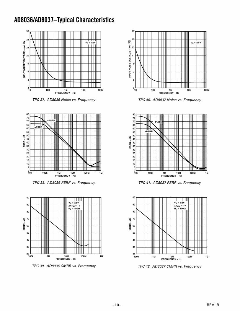
TPC 37. AD8036 Noise vs. Frequency
80
70
60
50
40
30
20
10
0
75
65
55
45
35
25
15
5
10k 100k 1G100M10M1MFREQUENCY – Hz
PS
RR
– d
B
–PSRR
+PSRR
TPC 38. AD8036 PSRR vs. Frequency
100
90
80
70
60
50
40
30
20100k 1G100M10M1M
FREQUENCY – Hz
CM
RR
– d
B
VS = 5V VCM = 1V RL = 100
TPC 39. AD8036 CMRR vs. Frequency
AD8036/AD8037–Typical Characteristics
100 100k10k1k10FREQUENCY – Hz
VS = 5V
INP
UT
NO
ISE
VO
LT
AG
E –
nV
/H
z
17
15
13
11
9
7
5
3
TPC 40. AD8037 Noise vs. Frequency
80
70
60
50
40
30
20
10
0
75
65
55
45
35
25
15
5
10k 100k 1G100M10M1MFREQUENCY – Hz
PS
RR
– d
B
–PSRR
+PSRR
TPC 41. AD8037 PSRR vs. Frequency
100
90
80
70
60
50
40
30
20100k 1G100M10M1M
FREQUENCY – Hz
CM
RR
– d
B
VS = 5V VCM = 1V RL = 100
TPC 42. AD8037 CMRR vs. Frequency
AD8036/AD8037
REV. B –11–
0.1MFREQUENCY – Hz
1.0M 100M10M 300M
RO
UT –
VS = 5V G = +1
1k
100
10
1
0.1
0.01
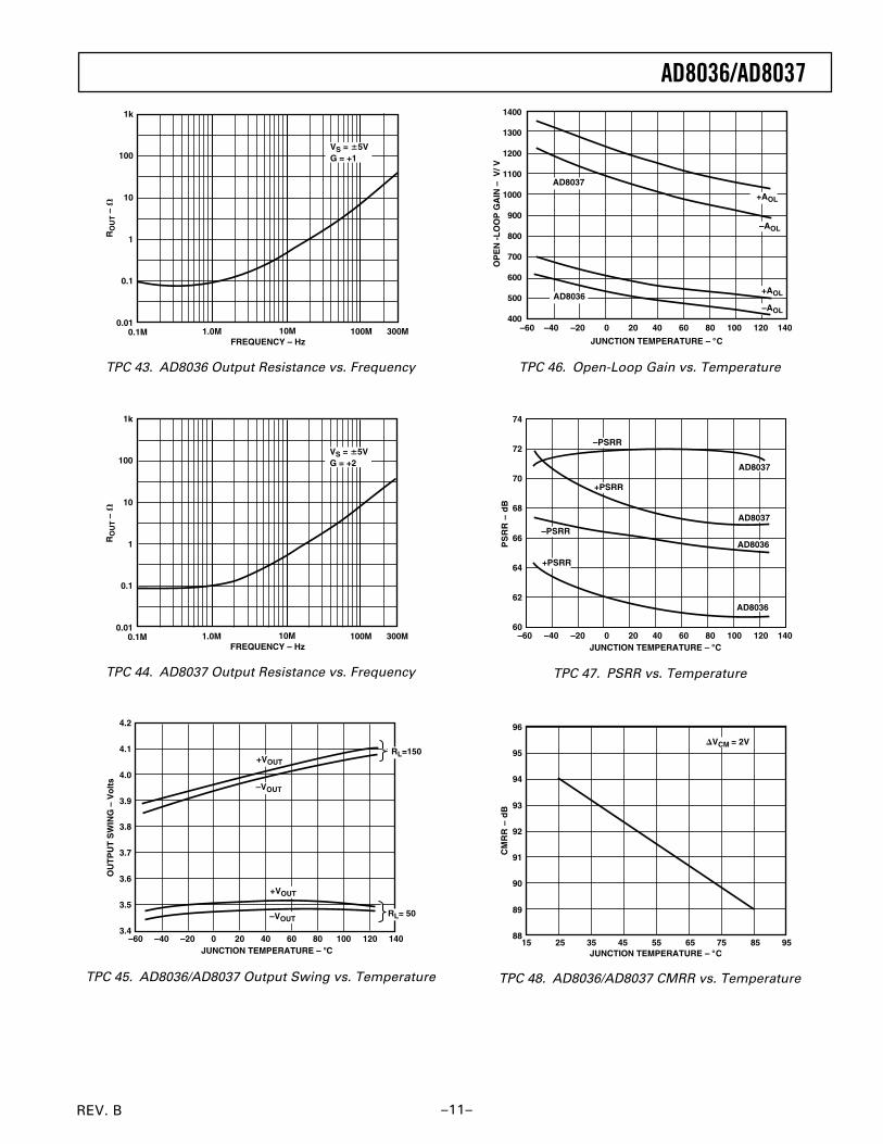
TPC 43. AD8036 Output Resistance vs. Frequency
0.1MFREQUENCY – Hz
1.0M 100M10M 300M
RO
UT –
VS = 5V G = +2
1k
100
10
1
0.1
0.01
TPC 44. AD8037 Output Resistance vs. Frequency
OU
TP
UT
SW
ING
– V
olt
s
JUNCTION TEMPERATURE – C
–VOUT
+VOUTRL=150
RL= 50–VOUT
+VOUT
4.2
4.1
4.0
3.9
3.8
3.7
3.6
3.5
3.4–60 –40 –20 0 20 40 60 80 100 120 140
TPC 45. AD8036/AD8037 Output Swing vs. Temperature
1400
1300
1200
1100
1000
900
800
700
600
500
400–60 –40 –20 0 20 40 60 80 100 120 140
–AOL
+AOL
–AOL
+AOLAD8036
AD8037
JUNCTION TEMPERATURE – C
OP
EN
-L
OO
P G
AIN
– V
/ V
TPC 46. Open-Loop Gain vs. Temperature
–60 –40 –20 0 20 40 60 80 100 120 140
PS
RR
– d
B
JUNCTION TEMPERATURE – C
–PSRR
AD8037
AD8036
AD8037
AD8036
+PSRR
+PSRR
–PSRR
74
72
70
68
66
64
62
60
TPC 47. PSRR vs. Temperature
15 25 35 45 55 65 75 85 95
CM
RR
– d
B
JUNCTION TEMPERATURE – C
VCM = 2V
96
95
94
93
92
91
90
89
88
TPC 48. AD8036/AD8037 CMRR vs. Temperature
REV. B–12–
AD8036/AD8037–Typical Characteristics
–60 –40 –20 0 20 40 60 80 100 120 140
SU
PP
LY
CU
RR
EN
T –
mA
JUNCTION TEMPERATURE – C
AD8036, VS = 6V
AD8036, VS = 5V
AD8037, VS = 6V
AD8037, VS = 5V
24
23
22
21
20
19
18
17
TPC 49. Supply Current vs. Temperature
–60 –40 –20 0 20 40 60 80 100 120 140JUNCTION TEMPERATURE – C
VS = 6V
VS = 5V
VS = 6V
VS = 5V
INP
UT
OF
FS
ET
VO
LT
AG
E –
mV
AD8037
AD8036
–2.50
–2.25
–2.00
–1.75
–1.50
–1.25
–1.00
–0.75
–0.50
TPC 50. Input Offset Voltage vs. Temperature
INPUT OFFSET VOLTAGE – mV
CO
UN
T
3 WAFER LOTSCOUNT = 632
FREQ. DIST
–6 –5 –4 –3 –2 –1 0 1 2 3 4
44
40
36
32
28
24
20
16
12
8
4
0
TPC 51. AD8036 Input Offset Voltage Distribution
–60 –40 –20 0 20 40 60 80 100 120 140JUNCTION TEMPERATURE – C
AD8037
AD8036
AD8036
SH
OR
T C
IRC
UIT
CU
RR
EN
T –
mA
AD8037 SINK
SOURCE
270
260
250
240
230
220
210
200
TPC 52. Short Circuit Current vs. Temperature
–60 –40 –20 0 20 40 60 80 100 120 140JUNCTION TEMPERATURE – C
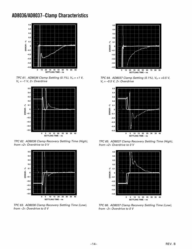
TPC 65. AD8037 Clamp Recovery Settling Time (High),from +2× Overdrive to 0 V
0 5 10 15 20 25 30 35 40SETTLING TIME – ns
ER
RO
R –
%
0.5
0.4
0.3
0.2
0.1
0
–0.1
–0.2
–0.3
–0.4
–0.5
TPC 66. AD8037 Clamp Recovery Settling Time (Low),from –2× Overdrive to 0 V
AD8036/AD8037
REV. B –15–
THEORY OF OPERATIONGeneralThe AD8036 and AD8037 are wide bandwidth, voltage feedbackclamp amplifiers. Since their open-loop frequency response fol-lows the conventional 6 dB/octave roll-off, their gain bandwidthproduct is basically constant. Increasing their closed-loop gainresults in a corresponding decrease in small signal bandwidth. Thiscan be observed by noting the bandwidth specification, betweenthe AD8036 (gain of 1) and AD8037 (gain of 2). The AD8036/AD8037 typically maintain 65 degrees of phase margin. Thishigh margin minimizes the effects of signal and noise peaking.
While the AD8036 and AD8037 can be used in either an invert-ing or noninverting configuration, the clamp function will onlywork in the noninverting mode. As such, this section shows con-nections only in the noninverting configuration. Applicationsthat require an inverting configuration will be discussed in theApplications section. In applications that do not require clamp-ing, Pins 5 and 8 (respectively VL and VH) may be left floating.See Input Clamp Amp Operation and Applications sectionsotherwise.
Feedback Resistor ChoiceThe value of the feedback resistor is critical for optimum perfor-mance on the AD8036 (gain +1) and less critical as the gainincreases. Therefore, this section is specifically targeted atthe AD8036.
At minimum stable gain (+1), the AD8036 provides optimumdynamic performance with RF = 140 Ω. This resistor acts onlyas a parasitic suppressor against damped RF oscillations thatcan occur due to lead (input, feedback) inductance and parasiticcapacitance. This value of RF provides the best combination ofwide bandwidth, low parasitic peaking, and fast settling time.
In fact, for the same reasons, a 100–130 Ω resistor should beplaced in series with the positive input for other AD8036 non-inverting configurations. The correct connection is shown inFigure 3.
RF
100 - 130
RTERM
RFRG
G = 1+
RG
VH
VL
+VS
–VS
VIN
VOUT
0.1F
10F
0.1F
10F
AD8036/AD8037
Figure 3. Noninverting Operation
For general voltage gain applications, the amplifier bandwidthcan be closely estimated as:
f 3 dB ≅ ωO
2π 1+ RF
RG
This estimation loses accuracy for gains of +2/–1 or lower dueto the amplifier’s damping factor. For these “low gain” cases,the bandwidth will actually extend beyond the calculated value(see Closed-Loop BW plots, TPCs 13 and 25).
Pulse ResponseUnlike a traditional voltage feedback amplifier, where the slewspeed is dictated by its front end dc quiescent current and gainbandwidth product, the AD8036 and AD8037 provide “ondemand” current that increases proportionally to the input“step” signal amplitude. This results in slew rates (1200 V/µs)comparable to wideband current feedback designs. This, com-bined with relatively low input noise current (2.1 pA/√Hz), givesthe AD8036 and AD8037 the best attributes of both voltage andcurrent feedback amplifiers.
Large Signal PerformanceThe outstanding large signal operation of the AD8036 andAD8037 is due to a unique, proprietary design architecture.In order to maintain this level of performance, the maximum350 V-MHz product must be observed, (e.g., @ 100 MHz,VO ≤ 3.5 V p-p).
Power Supply and Input Clamp BypassingAdequate power supply bypassing can be critical when optimiz-ing the performance of a high frequency circuit. Inductance inthe power supply leads can form resonant circuits that producepeaking in the amplifier’s response. In addition, if large currenttransients must be delivered to the load, then bypass capacitors(typically greater than 1 µF) will be required to provide the bestsettling time and lowest distortion. A parallel combination of atleast 4.7 µF, and between 0.1 µF and 0.01 µF, is recommended.Some brands of electrolytic capacitors will require a small seriesdamping resistor ≈4.7 Ω for optimum results.
When the AD8036 and AD8037 are used in clamping mode,and a dc voltage is connected to clamp inputs VH and VL, a 0.1 µFbypassing capacitor is required between each input pin andground in order to maintain stability.
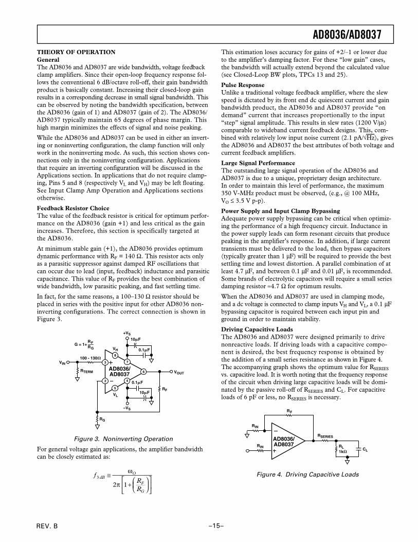
Driving Capacitive LoadsThe AD8036 and AD8037 were designed primarily to drivenonreactive loads. If driving loads with a capacitive compo-nent is desired, the best frequency response is obtained bythe addition of a small series resistance as shown in Figure 4.The accompanying graph shows the optimum value for RSERIES
vs. capacitive load. It is worth noting that the frequency responseof the circuit when driving large capacitive loads will be domi-nated by the passive roll-off of RSERIES and CL. For capacitiveloads of 6 pF or less, no RSERIES is necessary.
RL1k
RF
RIN
RSERIES
CL
AD8036/AD8037
RIN
Figure 4. Driving Capacitive Loads
REV. B–16–
AD8036/AD8037Operation of the AD8036 for negative input voltages and nega-tive clamp levels on VL is similar, with comparator CL control-ling S1. Since the comparators see the voltage on the +VIN pinas their common reference level, then the voltage VH and VL aredefined as “High” or “Low” with respect to +VIN. For example,if VIN is set to zero volts, VH is open, and VL is +1 V, compara-tor CL will switch S1 to “C,” so the AD8036 will buffer thevoltage on VL and ignore +VIN.
The performance of the AD8036 and AD8037 closely matchesthe ideal just described. The comparator’s threshold extendsfrom 60 mV inside the clamp window defined by the voltages onVL and VH to 60 mV beyond the window’s edge. Switch S1 isimplemented with current steering, so that A1’s +input makes acontinuous transition from say, VIN to VH as the input voltagetraverses the comparator’s input threshold from 0.9 V to 1.0 Vfor VH = 1.0 V.
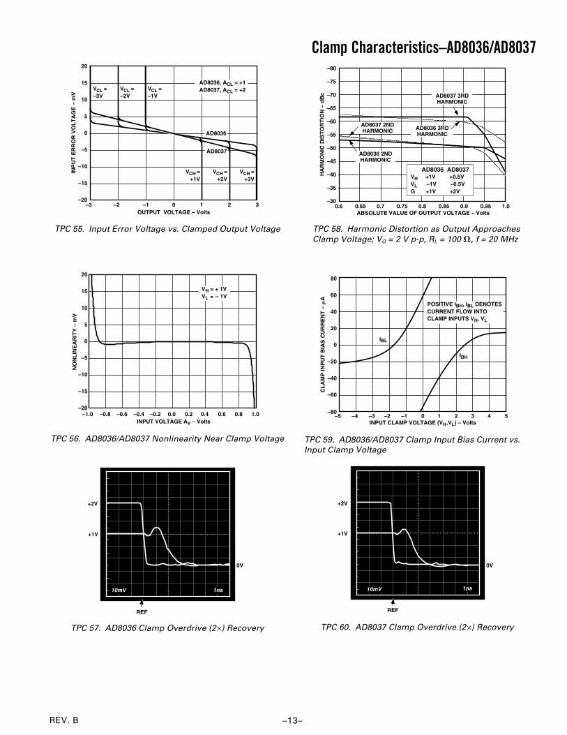
The practical effect of these nonidealities is to soften the transitionfrom amplification to clamping modes, without compromisingthe absolute clamp limit set by the CLAMPIN circuit. Figure 7is a graph of VOUT vs. VIN for the AD8036 and a typical outputclamp amplifier. Both amplifiers are set for G = +1 and VH = 1 V.
The worst case error between VOUT (ideally clamped) and VOUT
(actual) is typically 18 mV times the amplifier closed-loop gain.This occurs when VIN equals VH (or VL). As VIN goes aboveand/or below this limit, VOUT will settle to within 5 mV of theideal value.
In contrast, the output clamp amplifier’s transfer curve typicallywill show some compression starting at an input of 0.8 V, andcan have an output voltage as far as 200 mV over the clamp limit.In addition, since the output clamp in effect causes the am-plifier to operate open loop in clamp mode, the amplifier’s out-put impedance will increase, potentially causing additional errors.
The AD8036’s and AD8037’s CLAMPIN input clamp architec-ture works only for noninverting or follower applications and,since it operates on the input, the clamp voltage levels VH andVL, and input error limits will be multiplied by the amplifier’s
A
B
C
S1
RF140
A B C
0 1 0
1 0 0
0 0 1
S1
VIN > VH
VL ≤ VIN ≤ VH
VIN < VL
–VIN
+VIN
VH
VL
VOUT
+1
+1
+1
CH
CL
A1 A2+1
Figure 6. AD8036/AD8037 Clamp Amp System
0 5 10 15 20 25
RS
ER
IES –
CL– pF
40
30
20
10
Figure 5. Recommended RSERIES vs. Capacitive Load
INPUT CLAMPING AMPLIFIER OPERATIONThe key to the AD8036 and AD8037’s fast, accurate clamp andamplifier performance is their unique patent pending CLAMPINinput clamp architecture. This new design reduces clamp errorsby more than 10× over previous output clamp based circuits, aswell as substantially increasing the bandwidth, precision andversatility of the clamp inputs.
Figure 6 is an idealized block diagram of the AD8036 connectedas a unity gain voltage follower. The primary signal path com-prises A1 (a 1200 V/µs, 240 MHz high voltage gain, differentialto single-ended amplifier) and A2 (a G = +1 high current gainoutput buffer). The AD8037 differs from the AD8036 only inthat A1 is optimized for closed-loop gains of two or greater.
The CLAMPIN section is comprised of comparators CH andCL, which drive switch S1 through a decoder. The unity-gainbuffers in series with +VIN, VH, and VL inputs isolate the inputpins from the comparators and S1 without reducing bandwidthor precision.
The two comparators have about the same bandwidth as A1(240 MHz), so they can keep up with signals within the usefulbandwidth of the AD8036. To illustrate the operation of theCLAMPIN circuit, consider the case where VH is referenced to1 V, VL is open, and the AD8036 is set for a gain of +1, by con-necting its output back to its inverting input through the recom-mended 140 Ω feedback resistor. Note that the main signal pathalways operates closed loop, since the CLAMPIN circuit onlyaffects A1’s noninverting input.
If a 0 V to 2 V voltage ramp is applied to the AD8036’s +VIN
for the connection just described, VOUT should track +VIN
perfectly up to 1 V, then should limit at exactly 1 V as +VIN
continues to 2 V.
In practice, the AD8036 comes close to this ideal behavior. Asthe +VIN input voltage ramps from zero to 1 V, the output of thehigh limit comparator CH starts in the off state, as does the out-put of CL. When +VIN just exceeds VIN (ideally, by say 1 µV,practically by about 18 mV), CH changes state, switching S1from “A” to “B” reference level. Since the + input of A1 is nowconnected to VH, further increases in +VIN have no effect on theAD8036’s output voltage. In short, the AD8036 is now operat-ing as a unity-gain buffer for the VH input, as any variation inVH, for VH > 1 V, will be faithfully reproduced at VOUT.
AD8036/AD8037
REV. B –17–
closed-loop gain at the output. For instance, to set an outputlimit of ±1 V for an AD8037 operating at a gain of 3.0, VH andVL would need to be set to +0.333 V and –0.333 V, respectively.
The only restriction on using the AD8036’s and AD8037’s+VIN, VL, VH pins as inputs is that the maximum voltage differ-ence between +VIN and VH or VL should not exceed 6.3 V, andall three voltages be within the supply voltage range. For example,if VL is set at –3 V, then VIN should not exceed +3.3 V.
Figure 7. Output Clamp Error vs. Input Clamp Error
AD8036/AD8037 APPLICATIONSThe AD8036 and AD8037 use a unique input clamping circuitto perform the clamping function. As a result, they provide theclamping function better than traditional output clampingdevices and provide additional flexibility to perform otherunique applications.
There are, however, some restrictions on circuit configurations;and some calculations need to be performed in order to figurethe clamping level, as a result of clamping being performed atthe input stage.
The major restriction on the clamping feature of the AD8036/AD8037 is that clamping occurs only when using the amplifiersin the noninverting mode. To clamp in an inverting circuit, anadditional inverting gain stage is required. Another restriction isthat VH be greater than VL, and that each be within the outputvoltage range of the amplifier (±3.9 V). VH can go below groundand VL can go above ground as long as VH is kept higher than VL.
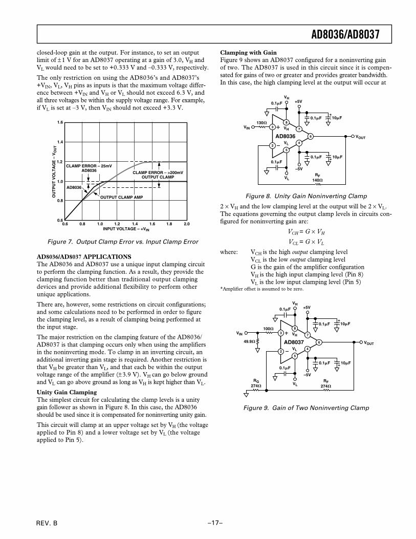
Unity Gain ClampingThe simplest circuit for calculating the clamp levels is a unitygain follower as shown in Figure 8. In this case, the AD8036should be used since it is compensated for noninverting unity gain.
This circuit will clamp at an upper voltage set by VH (the voltageapplied to Pin 8) and a lower voltage set by VL (the voltageapplied to Pin 5).
Clamping with GainFigure 9 shows an AD8037 configured for a noninverting gainof two. The AD8037 is used in this circuit since it is compen-sated for gains of two or greater and provides greater bandwidth.In this case, the high clamping level at the output will occur at
+5V
RF140
–5V
130
VH
VL
VIN
VOUT
0.1F 10F
0.1F
AD8036
0.1F 10F
VH
0.1F
VL
Figure 8. Unity Gain Noninverting Clamp
2 × VH and the low clamping level at the output will be 2 × VL.The equations governing the output clamp levels in circuits con-figured for noninverting gain are:
VCH = G × VH
VCL = G × VL
where: VCH is the high output clamping levelVCL is the low output clamping levelG is the gain of the amplifier configurationVH is the high input clamping level (Pin 8)VL is the low input clamping level (Pin 5)
*Amplifier offset is assumed to be zero.
+5V
RF274
–5V
100
VH
VL
VIN
VOUT
0.1F 10F
0.1F
AD8037
0.1F 10F
VH
0.1F
VLRG
274
49.9
Figure 9. Gain of Two Noninverting Clamp
REV. B–18–
AD8036/AD8037
Clamping with an OffsetSome op amp circuits are required to operate with an offsetvoltage. These are generally configured in the inverting modewhere the offset voltage can be summed in as one of the inputs.Since AD8036/AD8037 clamping does not function in the in-verting mode, it is not possible to clamp with this configuration.
Figure 10 shows a noninverting configuration of an AD8037that provides clamping and also has an offset. The circuit showsthe AD8037 as a driver for an AD9002, an 8-bit, 125 MSPSA/D converter and illustrates some of the considerations for us-ing an AD8037 with offset and clamping.
The analog input range of the AD9002 is from ground to –2 V.The input should not go more than 0.5 V outside this range inorder to prevent disruptions to the internal workings of the A/Dand to avoid drawing excess current. These requirements makethe AD8037 a prime candidate for signal conditioning.
When an offset is added to a noninverting op amp circuit, it isfed in through a resistor to the inverting input. The result is thatthe op amp must now operate at a closed-loop gain greater thanunity. For this circuit a gain of two was chosen which allows theuse of the AD8037. The feedback resistor, R2, is set at 301 Ωfor optimum performance of the AD8037 at a gain of two.
There is an interaction between the offset and the gain, so somecalculations must be performed to arrive at the proper values forR1 and R3. For a gain of two the parallel combination of resis-tors R1 and R3 must be equal to the feedback resistor R2. Thus
R1 × R3/R1 + R3 = R2 = 301 ΩThe reference used to provide the offset is the AD780 whoseoutput is 2.5 V. This must be divided down to provide the 1 Voffset desired. Thus
2.5 V × R1/(R1 + R3) = 1 V
When the two equations are solved simultaneously we get R1 =499 Ω and R3 = 750 Ω (using closest 1% resistor values in allcases). This positive 1 V offset at the input translates to a –1 Voffset at the output.
The usable input signal swing of the AD9002 is 2 V p-p. This iscentered about the –1 V offset making the usable signal rangefrom 0 V to –2 V. It is desirable to clamp the input signal so that
it goes no more than 100 mV outside of this range in either di-rection. Thus, the high clamping level should be set at +0.1 Vand the low clamping level should be set at –2.1 V as seen at theinput of the AD9002 (output of AD8037).
Because the clamping is done at the input stage of the AD8037,the clamping level as seen at the output is affected by not onlythe gain of the circuit as previously described, but also by theoffset. Thus, in order to obtain the desired clamp levels, VH
must be biased at +0.55 V while VL must be biased at –0.55 V.
The clamping levels as seen at the output can be calculated bythe following:
VCH = VOFF + G × VH
VCL = VOFF + G × VL
Where VOFF is the offset voltage that appears at the output.
The resistors used to generate the voltages for VH and VL shouldbe kept to a minimum in order to reduce errors due to clampbias current. This current is dependent on VH and VL (see TPC59) and will create a voltage drop across whatever resistance isin series with each clamp input. This extra error voltage ismultiplied by the closed-loop gain of the amplifier and can besubstantial, especially in high closed-loop gain configurations.A 0.1 µF bypass capacitor should be placed between inputclamp pins VH and VL and ground to ensure stable operation.
The 1N5712 Schottky diode is used for protection from forwardbiasing the substrate diode in the AD9002 during power-uptransients.
Programmable Pulse GeneratorThe AD8036/AD8037’s clamp output can be set accurately andhas a well controlled flat level. This along with wide bandwidthand high slew rate make them very well suited for programmablelevel pulse generators.
Figure 11 is a schematic for a pulse generator that can directlyaccept TTL generated timing signals for its input and generatepulses at the output up to 24 V p-p with 2500 V/µs slew rate.The output levels can be programmed to anywhere in the range–12 V to +12 V.
100
–0.5V to +0.5V
–2V to 0V
CLAMPINGRANGE
–2.1V to +0.1V
2.5V
+5V
10µF
–5.2V
1N5712
+5V
R2301
–5V
100
VH
VL
VIN
0.1F 10F
0.1F
AD8037
0.1F 10F
R1499
49.9
806
+5V
0.1F806
–5V
100
R3750
0.1F
0.1F
AD780
49.9
AD9002VIN = –2V TO 0V
SUBSTRATEDIODE
0.1F
Figure 10. Gain of Two, Noninverting with Offset AD8037 Driving an AD9002—8-Bit, 125 MSPS A/D Converter
AD8036/AD8037
REV. B –19–
The circuit uses an AD8037 operating at a gain of two with anAD811 to boost the output to the ±12 V range. The AD811 waschosen for its ability to operate with ±15 V supplies and its highslew rate.
R1 and R2 act as a level shifter to make the TTL signal levels beapproximately symmetrical above and below ground. This ensuresthat both the high and low logic levels will be clamped by theAD8037. For well controlled signal levels in the output pulse,the high and low output levels should result from the clampingaction of the AD8037 and not be controlled by either the highor low logic levels passing through a linear amplifier. For goodrise and fall times at the output pulse, a logic family with highspeed edges should be used.
The high logic levels are clamped at two times the voltage at VH,while the low logic levels are clamped at two times the voltageat VL. The output of the AD8037 is amplified by the AD811operating at a gain of 5. The overall gain of 10 will cause thehigh output level to be 10 times the voltage at VH, and the lowoutput level to be 10 times the voltage at VL.
High Speed, Full-Wave RectifierThe clamping inputs are additional inputs to the input stage ofthe op amp. As such they have an input bandwidth comparableto the amplifier inputs and lend themselves to some uniquefunctions when they are driven dynamically.
Figure 12 is a schematic for a full-wave rectifier, sometimescalled an absolute value generator. It works well up to 20 MHzand can operate at significantly higher frequencies with somedegradation in performance. The distortion performance is sig-nificantly better than diode based full-wave rectifiers, especiallyat high frequencies.
VOUT = VIN
+5V
RF274 –5V
100
VH
VL
VIN
0.1F 10F
AD8037
0.1F 10F
RG274
Figure 12. Full-Wave Rectifier
TTLIN
+15V
PULSEOUT
VH 10
VL 10
–15V
+5V
274
–5V
100
VH
VL
0.1F 10F
0.1F
AD8037
0.1F 10F
VH
0.1F
VL
274
1.3k
200
100
AD811
–15V
0.1F 10F
0.1F 10F
604
150
Figure 11. Programmable Pulse Generator
The circuit is configured as an inverting amplifier with a gainof one. The input drives the inverting amplifier and also directlydrives VL, the lower level clamping input. The high level clamp-ing input, VH, is left floating and plays no role in this circuit.
When the input is negative, the amplifier acts as a regular unity-gain inverting amplifier and outputs a positive signal at the sameamplitude as the input with opposite polarity. VL is driven nega-tive by the input, so it performs no clamping action, because thepositive output signal is always higher than the negative leveldriving VL.
When the input is positive, the output result is the sum of twoseparate effects. First, the inverting amplifier multiplies the inputby –1 because of its unity-gain inverting configuration. Thiseffectively produces an offset as explained above, but with adynamic level that is equal to –1 times the input.
Second, although the positive input is grounded (through 100 Ω),the output is clamped at two times the voltage applied to VL (apositive, dynamic voltage in this case). The factor of two isbecause the noise gain of the amplifier is two.
The sum of these two actions results in an output that is equalto unity times the input signal for positive input signals, see Fig-ure 13. For a input/output scope photo with an input signal of20 MHz and amplitude ±1 V, see Figure 14.
INPUT
FULL WAVERECTIFIEDOUTPUT
LOWERCLAMPINGLEVEL WITHNO NEG INPUT
OUTPUT
LOWERCLAMPINGLEVEL
–1 INPUT
Figure 13.
REV. B–20–
AD8036/AD8037
Figure 14. Full-Wave Rectifier Scope
Thus for either positive or negative input signals, the output isunity times the absolute value of the input signal. The circuitcan be easily configured to produce the negative absolute valueof the input by applying the input to VH instead of VL.
The circuit can get to within about 40 mV of ground during thetime when the input crosses zero. This voltage is fixed over awide frequency range and is a result of the switching betweenthe conventional op amp input and the clamp input. But becausethere are no diodes to rapidly switch from forward to reverse bias,the performance far exceeds that of diode based full wave rectifiers.
The 40 mV offset mentioned can be removed by adding an off-set to the circuit. A 27.4 kΩ input resistor to the inverting inputwill have a gain of 0.01, while changing the gain of the circuitby only 1%. A plus or minus 4 V dc level (depending on thepolarity of the rectifier) into this resistor will compensate forthe offset.
Full wave rectifiers are useful in many applications includingAM signal detection, high frequency ac voltmeters and variousarithmetic operations.
Amplitude ModulatorIn addition to being able to be configured as an amplitudedemodulator (AM detector), the AD8037 can also be config-ured as an amplitude modulator as shown in Figure 15.
CARRIER IN
VH
AM OUT
MODULATION IN
+5V
RF274 –5V
100
VH
VL
0.1F 10F
AD8037
0.1F 10F
RG274
Figure 15. Amplitude Modulator
The positive input of the AD8037 is driven with a square waveof sufficient amplitude to produce clamping action at both thehigh and low levels. This is the higher frequency carrier signal.
The modulation signal is applied to both the input of a unitygain inverting amplifier and to VL, the lower clamping input.VH is biased at 0.5 V dc.
To understand the circuit operation, it is helpful to first con-sider a simpler circuit. If both VL and VH were dc biased at–0.5 V and the carrier and modulation inputs driven as above,the output would be a 2 V p-p square wave at the carrier fre-quency riding on a waveform at the modulating frequency. Theinverting input (modulation signal) is creating a varying offset tothe 2 V p-p square wave at the output. Both the high and lowlevels clamp at twice the input levels on the clamps because thenoise gain of the circuit is two.
When VL is driven by the modulation signal instead of being heldat a dc level, a more complicated situation results. The resultingwaveform is composed of an upper envelope and a lower enve-lope with the carrier square wave in between. The upper andlower envelope waveforms are 180° out of phase as in a typicalAM waveform.
The upper envelope is produced by the upper clamp level beingoffset by the waveform applied to the inverting input. This offsetis the opposite polarity of the input waveform because of theinverting configuration.
The lower envelope is produced by the sum of two effects. First,it is offset by the waveform applied to the inverting input as inthe case of the simplified circuit above. The polarity of this off-set is in the same direction as the upper envelope. Second, theoutput is driven in the opposite direction of the offset at twicethe offset voltage by the modulation signal being applied to VL.This results from the noise gain being equal to two, and sincethere is no inversion in this connection, it is opposite polarityfrom the offset.
The result at the output for the lower envelope is the sum ofthese two effects, which produces the lower envelope of anamplitude modulated waveform. See Figure 16.
Figure 16. AM Waveform
The depth of modulation can be modified in this circuit bychanging the amplitude of the modulation signal. This changesthe amplitude of the upper and lower envelope waveforms.
The modulation depth can also be changed by changing the dcbias applied to VH. In this case the amplitudes of the upper andlower envelope waveforms stay constant, but the spacing betweenthem changes. This alters the ratio of the envelope amplitude tothe amplitude of the overall waveform.
AD8036/AD8037
REV. B –21–
Layout ConsiderationsThe specified high speed performance of the AD8036 andAD8037 requires careful attention to board layout and componentselection. Proper RF design techniques and low pass parasiticcomponent selection are mandatory.
The PCB should have a ground plane covering all unusedportions of the component side of the board to provide a lowimpedance path. The ground plane should be removed from thearea near the input pins to reduce stray capacitance.
Chip capacitors should be used for supply and input clampbypassing (see Figure 17). One end should be connected tothe ground plane and the other within 1/8 inch of each powerand clamp pin. An additional large (0.47 µF–10 µF) tantalumelectrolytic capacitor should be connected in parallel, thoughnot necessarily so close, to supply current for fast, large signalchanges at the output.
The feedback resistor should be located close to the invertinginput pin in order to keep the stray capacitance at this node to aminimum. Capacitance variations of less than 1 pF at the invert-ing input will significantly affect high speed performance.
Stripline design techniques should be used for long signal traces(greater than about 1 inch). These should be designed with acharacteristic impedance of 50 Ω or 75 Ω and be properly termi-nated at each end.
Evaluation BoardAn evaluation board for both the AD8036 and AD8037 isavailable that has been carefully laid out and tested to demon-strate that the specified high speed performance of the devicecan be realized. For ordering information, please refer to theOrdering Guide.
The layout of the evaluation board can be used as shown orserve as a guide for a board layout.
IN
RO
1k
VOUT
0.1F
AD8036/AD8037
VH
0.1F
VL
RS
–VS
+VS
–VS
+VS
RG
RF
1k
–VS
+VS
RT
NONINVERTING CONFIGURATION
C510F
+VS
–VS
C30.1F
C10.01F
C610F
C40.1F
C20.01F
OPTIONAL
SUPPLY BYPASSING
Figure 17. Noninverting Configurations for EvaluationBoards