coatings Article A Parametric Three-Dimensional Phase-Field Study of the Physical Vapor Deposition Process of Metal Thin Films Aiming at Quantitative Simulations Shenglan Yang 1 , Jing Zhong 1, *, Miao Chen 2 and Lijun Zhang 1, * 1 State Key Lab of Powder Metallurgy, Central South University, Changsha 410083, China; [email protected]2 Institute of Nuclear Physics and Chemistry, China Academy of Engineering Physics, Mianyang 621900, China; [email protected]* Correspondence: [email protected] (J.Z.); [email protected] (L.Z.); Tel.: +86-7318-883-6812 (L.Z.) Received: 4 September 2019; Accepted: 19 September 2019; Published: 25 September 2019 Abstract: In this paper, a parametric three-dimensional (3D) phase-field study of the physical vapor deposition process of metal thin films was performed aiming at quantitative simulations. The effect of deposition rate and model parameters on the microstructure of deposited thin films was investigated based on more than 200 sets of 3D phase-field simulations, and a quantitative relationship between the deposition rate and model parameters was established. After that, the heat maps corresponding to the experimental atomic force microscopy images were plotted for characterization of the surface roughness. Different roughness parameters including the arithmetic average roughness (R a ), root mean square roughness (R q ), skewness (R sk ), and kurtosis (R ku ), as well as the ratio of R q to R a were calculated and carefully analyzed. A quantitative relationship between the surface roughness and the deposition rate and model parameters was obtained. Moreover, the calculated R q to R a ratios for the thin films at the deposition rates of 0.22 and 1.0 nm s -1 agreed very well with the experimental data of the deposited Mo and Ti thin films. Finally, further discussion about the correlative behaviors between the surface roughness and the density was proposed for reasoning the shadowing effect as well as the formation of voids during the thin film production. Keywords: phase-field modeling; physical vapor deposition; microstructure; deposition rate; surface roughness 1. Introduction Physical vapor deposition (PVD) is a well-known technology that is widely used for the deposition of various coatings including metal thin films, such as Mo and Cu thin films for microelectronic devices [1,2], Ti thin films for biomedical applications [3] and Zr thin films for nuclear industry [4], thermal barrier coatings for turbine engines [5–7], as well as wear and oxidation resistance coatings for machining tools [8,9]. In industry, the PVD coating properties significantly affecting the coated tool life can be tuned by applying different deposition parameters. Thus, numerous experiments have been conducted on the influence of different process parameters, such as the bias voltage, gas pressure, substrate temperature, pretreatments, etc., on the coating properties targeting the PVD coatings with optimal properties [10–13]. Moreover, the computational fluid dynamics (CFD) simulations have also been performed on some PVD coatings with a focus on the study of the fluid flow dynamics, temperature, pressure, the velocity of distribution of the species into the reactor, and others, which can help to design process conditions of the PVD processing, and thus optimize the coating Coatings 2019, 9, 607; doi:10.3390/coatings9100607 www.mdpi.com/journal/coatings
Transcript
coatings
Article
A Parametric Three-Dimensional Phase-Field Studyof the Physical Vapor Deposition Process of MetalThin Films Aiming at Quantitative Simulations
Shenglan Yang 1 , Jing Zhong 1,*, Miao Chen 2 and Lijun Zhang 1,*1 State Key Lab of Powder Metallurgy, Central South University, Changsha 410083, China;
[email protected] Institute of Nuclear Physics and Chemistry, China Academy of Engineering Physics,
Received: 4 September 2019; Accepted: 19 September 2019; Published: 25 September 2019
Abstract: In this paper, a parametric three-dimensional (3D) phase-field study of the physical vapordeposition process of metal thin films was performed aiming at quantitative simulations. The effect ofdeposition rate and model parameters on the microstructure of deposited thin films was investigatedbased on more than 200 sets of 3D phase-field simulations, and a quantitative relationship betweenthe deposition rate and model parameters was established. After that, the heat maps correspondingto the experimental atomic force microscopy images were plotted for characterization of the surfaceroughness. Different roughness parameters including the arithmetic average roughness (Ra), rootmean square roughness (Rq), skewness (Rsk), and kurtosis (Rku), as well as the ratio of Rq to Ra werecalculated and carefully analyzed. A quantitative relationship between the surface roughness andthe deposition rate and model parameters was obtained. Moreover, the calculated Rq to Ra ratios forthe thin films at the deposition rates of 0.22 and 1.0 nm s−1 agreed very well with the experimentaldata of the deposited Mo and Ti thin films. Finally, further discussion about the correlative behaviorsbetween the surface roughness and the density was proposed for reasoning the shadowing effect aswell as the formation of voids during the thin film production.
Physical vapor deposition (PVD) is a well-known technology that is widely used for the depositionof various coatings including metal thin films, such as Mo and Cu thin films for microelectronicdevices [1,2], Ti thin films for biomedical applications [3] and Zr thin films for nuclear industry [4],thermal barrier coatings for turbine engines [5–7], as well as wear and oxidation resistance coatingsfor machining tools [8,9]. In industry, the PVD coating properties significantly affecting the coatedtool life can be tuned by applying different deposition parameters. Thus, numerous experimentshave been conducted on the influence of different process parameters, such as the bias voltage,gas pressure, substrate temperature, pretreatments, etc., on the coating properties targeting thePVD coatings with optimal properties [10–13]. Moreover, the computational fluid dynamics (CFD)simulations have also been performed on some PVD coatings with a focus on the study of the fluid flowdynamics, temperature, pressure, the velocity of distribution of the species into the reactor, and others,which can help to design process conditions of the PVD processing, and thus optimize the coating
properties [14–17]. However, in fact, PVD is a considerably sophisticated process and it is extremelydifficult to improve the performance of the coating just through variation of the process parameters.As is well known, the microstructure evolution during the PVD process plays an important role inthe properties of coatings [18–23]. Therefore, it is necessary to perform quantitative descriptionsof the microstructure evolution of coatings and establish the relationship between various processparameters and their microstructures during the PVD process in order to further design the coatingswith higher quality.
Up to now, various researchers have devoted themselves to experimental investigations of theeffects of process parameters of PVD on the microstructure of coatings, conducting the correspondingmicrostructure characterization and preparing the coatings with significantly different microstructuresby using different process parameters, such as the PVD chamber temperature, the substrate thickness,the substrate rotation, the incident vapor rate and angle, and the deposition time [2,5,24,25]. Typically,the experimental studies are time-consuming and costly, and computer simulations can help to realizethe investigation on the microstructure of coatings during PVD. In fact, a large number of Monte Carlo(MC) simulations of PVD coatings have been performed, but most of them mainly focused on the effectsof the incident vapor angle and substrate temperature on the orientation of columns, and the porosityand grain size [26–29]. Moreover, the surface roughness of coatings strongly influences their properties,such as the wear resistance of coatings for machining tools [30], electric conductivity of thin filmsfor microelectronic devices [31], and biocompatibility of thin films for biomedical materials [32,33],however, the MC simulations [26–29] were limited to the two-dimension (2D) simulations and thuswere not adequate to describe the surface roughness of coatings. Despite the above-mentionedefforts, the quantitative relationship between the coating microstructure and the process parametershas not been established up to now. In addition to MC simulations, the phase-field modeling hasalso been applied to simulate the thin film growth during PVD. Keblinski et al. [34] developed aphase-field model for the growth of interfaces and applied the model to simulate the solid film growthduring PVD with different incident vapor fluxes. Coupling the interface growth phase-field model byKeblinski et al. [34] with the phase-field model for solidification of polycrystalline materials developedby Warren et al. [35], Stewart and Spearot [36,37] developed a phase-field model for the evolution ofsingle-phase polycrystalline thin films and utilized the model to investigate the influence of modelparameters on the grain size, as well as porosity and grain orientation. However, dimensionlessparameters were used in the models [37,38] for PVD. Thus, the simulated results were only qualitative,and cannot be compared with the actual experimental microstructure, not to mention guiding thedesign of high-quality coatings.
Consequently, the phase-field model developed by Keblinski et al. [34] was used in the presentwork to perform a three-dimensional (3D) study of the PVD process of metal thin films, aiming atthe quantitative simulations. First, a parametric study was conducted, resulting in the quantitativerelationship between the model parameters and deposition rates. Second, a series of 3D phase-fieldsimulation of the PVD process of metal thin films was carried out. The effect of deposition rate andtime on the surface roughness and microstructure of the deposited metal thin film was systematicallyanalyzed and compared with the existing experimental results.
2. Phase-field Model for the PVD Process of Metal Thin Film
The interface growth phase-field model of Keblinski et al. [34] can be used to describe thedynamics and morphology of a growing solid film during PVD and has been demonstrated to naturallycapture prominent physical processes during PVD, such as: (i) arbitrary surface morphology formation,(ii) surface tension and diffusion, and (iii) nonlocal shadowing effects. Two field variables are introducedin the model, i.e., φ(r, t) and g(r, t). The field variable φ(r, t) describes the evolution of growing thinfilm solid, where φ(r, t) ≈ 1 describes the solid phase, φ(r, t) ≈ −1 describes the vapor phase, and φ(r, t)≈ 0 describes the solid–vapor interface. The field variable g(r, t) that is always greater than or equal to0 (i.e., g(r, t) ≥ 0) and does not contribute to the free energy of the system, describes the local density of
Coatings 2019, 9, 607 3 of 15
the incident vapor, where g(r, t) ≈ 0 describes the presence of no vapor. The free energy functional wasconstructed based on the field variables φ(r, t) and their gradients and written as,
F =
∫Ω
−
12φ(r, t)2 +
14φ(r, t)4 + a(∇φ(r, t))2
(1)
where the first two terms in Equation (1) provide a double-well potential describing the bulk solid andvapor phases, the third term in Equation (1) provides an energy penalty for the presence of solid-vaporinterface, and a is the interfacial gradient coefficient, which is related to surface tension. On thebasis of Equation (1), the evolution equations for PVD of a single-phase polycrystalline thin film canbe determined
.φ = ∇2 δF
δφ+ B(∇φ)2g + C
√(∇φ)2gη (2)
.g = ∇[D∇g−Ag] − B(∇φ)2g (3)
where Equation (2) describes the growth of films and Equation (3) describes the transport of thedeposition vapor. The first term in Equation (2) provides Chan–Hilliard dynamics, which allows forarbitrary surface formation while simultaneously capturing surface diffusion. The second term inEquation (2) is the source term that couples Equation (2) with Equation (3), which allows the growth ofthe solid phase, i.e., φ(r, t), to occur at the expense of the incident vapor phase, i.e., g(r, t). The last termin Equation (2) provides surface fluctuations through a Gaussian noise distribution, η(r, t). The firstterm in Equation (3) is the diffusion equation modified by the presence of an external force, A, andthe second term in Equation (3), which is the negative of second term in Equation (2), is a sink thatremoves the vapor in regions that have been converted into the solid phase. The coefficient B controlsthe growth rate, C controls the noise amplitude, D is the diffusion coefficient, and A provides thedirection and strength of incident vapor.
3. Model Parameters and Numerical Solution
The PVD process is influenced by multiple process factors, i.e., the speed of the incident vapor,surface diffusion of the solid phase, interfacial gradient coefficient, and so on. In order to compare thesimulated results with experimental data and obtain the quantitative relationship between processparameters and microstructures of deposited thin films, there is a need to parameterize the modelparameters. The interfacial gradient coefficient, a (J m2) in Equation (1), is used to characterize thecontribution of surface energy from the interface between the solid and vapor phases. The coefficientB (m2 s−1) controls the conversion of the g field into the φ field in the interfacial region leading tog(r, t) ≈ 0 below the interface (φ(r, t) ≈ 1) and thus can be quantified as the generated interface areaper unit time, named the gas–solid transition velocity. The noise amplitude coefficient, C (J m−1),provides sufficient noise at the thin film surface to allow the formation of surface variations andfeatures. The parameter D (m2 s−1) is the diffusion coefficient controlling the surface diffusion of thesolid thin film. The parameter A is the incident vapor vector including the incident vapor rate A (m s−1)and angle (i.e., A = Ar). The direction of the incident vapor in the present simulation is perpendicular
to the substrate (i.e., A = A^z).
In order to perform the 3D phase-field simulation of the PVD process, an initially flat substrateis constructed in the present work along the entire x−y plane in the z direction with a thickness lessthan 1/10 of the grid points of the z axis, where φ(r, 0) = 1 and g(r, 0) = 0. The region above thesubstrate is taken to vacuum, where φ(r, 0) = −1 and g(r, 0) = g0. The equations of motion describedin Equations (2) and (3) are discretized and solved on a uniform three-dimensional mesh. For theseequations, the periodic condition is applied in the direction parallel to the substrate (i.e., x and y axes),while the no-flux and fixed conditions are applied at the lower and upper boundaries of the directionperpendicular to substrate (i.e., z axis). During the simulation, the g = g0 condition is maintained at theupper boundary of the z direction providing a constant downward flux Ag during PVD.
Coatings 2019, 9, 607 4 of 15
The model parameters in Equations (2) and (3) and numerical parameters for simulations thatare fixed across the simulations in this work are summarized in Table 1. Parameters including thevaried gas–solid transition velocity B, incident vapor rate A, and simulation dimension are presentedin corresponding simulation results.
Table 1. List of the model and numerical parameters used in the present phase-field simulations.
Gaussian noise factor η 0.5Supplied incident vapor g0 1.0
4. Results and Discussion
4.1. Relationship Between Deposition Rate and Model Parameters
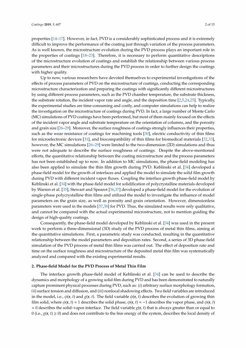
The deposition rate of the thin films during the PVD process play an important role in controllingtheir properties. Extensive reports and discussions about the relationship between the deposition rateand the microstructure and surface morphologies of thin film are available. In this work, over 200 3Dphase-field simulations for thin films during PVD were performed to obtain the relationship betweenthe deposition rate and model parameters. Specifically, simulations were performed in a 3D domainof 48× 48× 48 grid points. The microstructures of the 3D simulations for thin films deposited withthree different deposition rates (i.e., 0.39, 1.0, and 1.6 nm s−1) corresponding to the different gas–solidtransition velocity and incident vapor rate at the deposition time of 10 min are displayed in Figure 1for demonstration. As shown in Figure 1, the different gas–solid transition velocities and incidentvapor rates corresponding to the same deposition rate result in different microstructures and surfacetopographies. The thin film deposited with a low deposition rate is denser than the one deposited witha high deposition rate. For the deposition rate of 0.39 nm s−1, the density of solid thin film does notsignificantly change with the gas–solid transition velocity and incident vapor rate. For the depositionrates of 1.0 and 1.6 nm s−1, the decreased incident vapor rate and the increased gas–solid transitionvelocity result in the thin film with lower density. Furthermore, there exist more columnar featuresof surface of the thin films with the higher deposition rate, especially for the thin film with highergas–solid transition velocity (see Figure 1g).
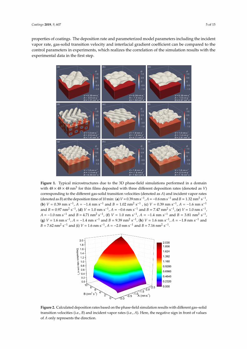
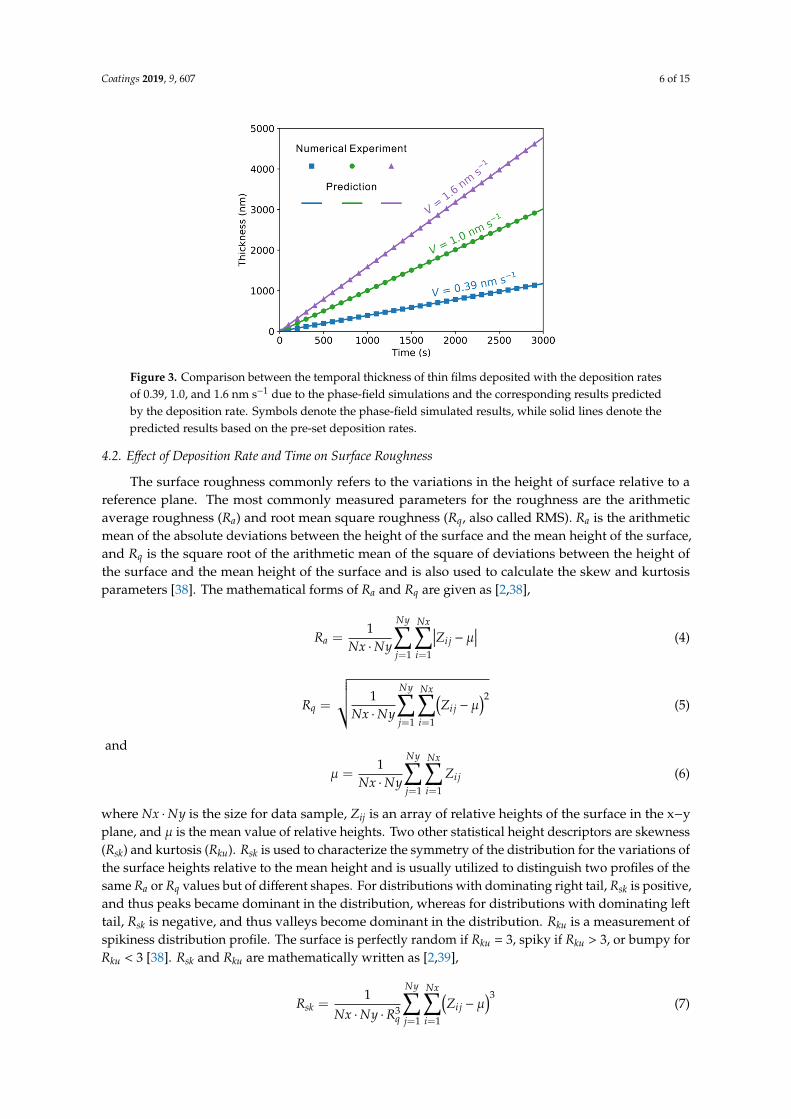
Figure 2 displays the calculated deposition rates from the phase-field simulation results withdifferent gas–solid transition velocities and incident vapor rates. As shown in Figure 2, the depositionrate decreases as the gas–solid transition velocity and incident vapor rate decrease. The deposition rateis relatively smaller and does not significantly change with the incident vapor rate when the gas–solidtransition velocity is less than 1.0 nm2 s−1. Furthermore, it is obvious that the same deposition rate canbe obtained through simulations with different sets of gas–solid transition velocities and incident vaporrates. For the same deposition rate, the required incident vapor rate is smaller when the gas–solidtransition velocity is higher, whereas the required gas–solid transition velocity is smaller when theincident vapor rate is higher. Moreover, the deposition rates can be conveniently used to predict thetemporal thin film thickness that are of interest in industry. The relationship between the thicknessand deposition time due to the numerical simulations and the corresponding values predicted by thedeposition rate are presented in Figure 3. As can be seen in the figure, both are in excellent agreementwith each other.
The incident vapor rate provides the information on the amount of the vapor reaching the interfacebetween gas and solid phase and the incident angle of the vapor. The gas-solid transition velocity isrelated to the characteristics of the film itself which is influenced by the deposition condition suchas the gas pressure. The deposition rate is the efficient parameter usually used to characterize the
Coatings 2019, 9, 607 5 of 15
properties of coatings. The deposition rate and parameterized model parameters including the incidentvapor rate, gas-solid transition velocity and interfacial gradient coefficient can be compared to thecontrol parameters in experiments, which realizes the correlation of the simulation results with theexperimental data in the first step.Coatings 2019, 9, x FOR PEER REVIEW 5 of 15
Figure 1. Typical microstructures due to the 3D phase-field simulations performed in a domain with48 48 48× × nm3 for thin films deposited with three different deposition rates (denoted as V) corresponding to the different gas-solid transition velocities and incident vapor rates at the deposition time of 10 min.
Figure 2. Calculated deposition rates based on the phase-field simulation results with different gas–solid transition velocities (i.e., B) and incident vapor rates (i.e., A). Here, the negative sign in front of values of A only represents the direction.
Figure 1. Typical microstructures due to the 3D phase-field simulations performed in a domainwith 48 × 48 × 48 nm3 for thin films deposited with three different deposition rates (denoted as V)corresponding to the different gas-solid transition velocities (denoted as A) and incident vapor rates(denoted as B) at the deposition time of 10 min: (a) V = 0.39 nm s−1, A =−0.6 nm s−1 and B = 1.32 nm2 s−1,(b) V = 0.39 nm s−1, A = −1.4 nm s−1 and B = 1.02 nm2 s−1 , (c) V = 0.39 nm s−1, A = −1.6 nm s−1
and B = 0.97 nm2 s−1, (d) V = 1.0 nm s−1, A = −0.6 nm s−1 and B = 7.47 nm2 s−1, (e) V = 1.0 nm s−1,A = −1.0 nm s−1 and B = 4.71 nm2 s−1, (f) V = 1.0 nm s−1, A = −1.4 nm s−1 and B = 3.81 nm2 s−1,(g) V = 1.6 nm s−1, A = −1.4 nm s−1 and B = 9.39 nm2 s−1, (h) V = 1.6 nm s−1, A = −1.8 nm s−1 andB = 7.62 nm2 s−1 and (i) V = 1.6 nm s−1, A = −2.0 nm s−1 and B = 7.16 nm2 s−1.
Coatings 2019, 9, x FOR PEER REVIEW 5 of 15
Figure 1. Typical microstructures due to the 3D phase-field simulations performed in a domain with48 48 48× × nm3 for thin films deposited with three different deposition rates (denoted as V) corresponding to the different gas-solid transition velocities and incident vapor rates at the deposition time of 10 min.
Figure 2. Calculated deposition rates based on the phase-field simulation results with different gas–solid transition velocities (i.e., B) and incident vapor rates (i.e., A). Here, the negative sign in front of values of A only represents the direction.
Figure 2. Calculated deposition rates based on the phase-field simulation results with different gas–solidtransition velocities (i.e., B) and incident vapor rates (i.e., A). Here, the negative sign in front of valuesof A only represents the direction.
Coatings 2019, 9, 607 6 of 15
Coatings 2019, 9, x FOR PEER REVIEW 6 of 15
Figure 3. Comparison between the temporal thickness of thin films deposited with the deposition rates of 0.39, 1.0, and 1.6 nm s−1 due to the phase-field simulations and the corresponding results predicted by the deposition rate. Symbols denote the phase-field simulated results, while solid lines denote the predicted results based on the pre-set deposition rates.
4.2. Effect of Deposition Rate and Time on Surface Roughness
The surface roughness commonly refers to the variations in the height of surface relative to a reference plane. The most commonly measured parameters for the roughness are the arithmetic average roughness (Ra) and root mean square roughness (Rq, also called RMS). Ra is the arithmetic mean of the absolute deviations between the height of the surface and the mean height of the surface, and Rq is the square root of the arithmetic mean of the square of deviations between the height of the surface and the mean height of the surface and is also used to calculate the skew and kurtosis parameters [38]. The mathematical forms of Ra and Rq are given as [2,38],
1 1
1 Ny Nx
a ijj i
R ZNx Ny
μ= =
= −⋅ (4)
( )2
1 1
1 Ny Nx
q ijj i
R ZNx Ny
μ= =
= −⋅ (5)
and
1 1
1 Ny Nx
ijj i
ZNx Ny
μ= =
=⋅ (6)
where Nx Ny⋅ is the size for data sample, Zij is an array of relative heights of the surface in the x−y plane, and μ is the mean value of relative heights. Two other statistical height descriptors are skewness (Rsk) and kurtosis (Rku). Rsk is used to characterize the symmetry of the distribution for the variations of the surface heights relative to the mean height and is usually utilized to distinguish two profiles of the same Ra or Rq values but of different shapes. For distributions with dominating right tail, Rsk is positive, and thus peaks became dominant in the distribution, whereas for distributions with dominating left tail, Rsk is negative, and thus valleys become dominant in the distribution. Rku is a measurement of spikiness distribution profile. The surface is perfectly random if Rku = 3, spiky if Rku > 3, or bumpy for Rku < 3 [38]. Rsk and Rku are mathematically written as [2,39],
( )3
31 1
1 Ny Nx
sk ijj iq
R ZNx Ny R
μ= =
= −⋅ ⋅ (7)
( )4
41 1
1 3Ny Nx
ku ijj iq
R ZNx Ny R
μ= =
= − −⋅ ⋅ (8)
To systematically analyze surface roughness for thin films, several phase-field simulations with three different deposition rates of 0.1, 0.5, and 1.0 nm s−1 were performed in a larger 3D domain of
Figure 3. Comparison between the temporal thickness of thin films deposited with the deposition ratesof 0.39, 1.0, and 1.6 nm s−1 due to the phase-field simulations and the corresponding results predictedby the deposition rate. Symbols denote the phase-field simulated results, while solid lines denote thepredicted results based on the pre-set deposition rates.
4.2. Effect of Deposition Rate and Time on Surface Roughness
The surface roughness commonly refers to the variations in the height of surface relative to areference plane. The most commonly measured parameters for the roughness are the arithmeticaverage roughness (Ra) and root mean square roughness (Rq, also called RMS). Ra is the arithmeticmean of the absolute deviations between the height of the surface and the mean height of the surface,and Rq is the square root of the arithmetic mean of the square of deviations between the height ofthe surface and the mean height of the surface and is also used to calculate the skew and kurtosisparameters [38]. The mathematical forms of Ra and Rq are given as [2,38],
Ra =1
Nx ·Ny
Ny∑j=1
Nx∑i=1
∣∣∣Zi j − µ∣∣∣ (4)
Rq =
√√√√1
Nx ·Ny
Ny∑j=1
Nx∑i=1
(Zi j − µ
)2(5)
and
µ =1
Nx ·Ny
Ny∑j=1
Nx∑i=1
Zi j (6)
where Nx ·Ny is the size for data sample, Zij is an array of relative heights of the surface in the x−yplane, and µ is the mean value of relative heights. Two other statistical height descriptors are skewness(Rsk) and kurtosis (Rku). Rsk is used to characterize the symmetry of the distribution for the variations ofthe surface heights relative to the mean height and is usually utilized to distinguish two profiles of thesame Ra or Rq values but of different shapes. For distributions with dominating right tail, Rsk is positive,and thus peaks became dominant in the distribution, whereas for distributions with dominating lefttail, Rsk is negative, and thus valleys become dominant in the distribution. Rku is a measurement ofspikiness distribution profile. The surface is perfectly random if Rku = 3, spiky if Rku > 3, or bumpy forRku < 3 [38]. Rsk and Rku are mathematically written as [2,39],
Rsk =1
Nx ·Ny ·R3q
Ny∑j=1
Nx∑i=1
(Zi j − µ
)3(7)
Coatings 2019, 9, 607 7 of 15
Rku =1
Nx ·Ny ·R4q
Ny∑j=1
Nx∑i=1
(Zi j − µ
)4− 3 (8)
To systematically analyze surface roughness for thin films, several phase-field simulations withthree different deposition rates of 0.1, 0.5, and 1.0 nm s−1 were performed in a larger 3D domain of192 × 192 × 64 grid points. Figure 4 shows a typical 3D microstructure for the thin film due to thelarger-size phase-field simulations with the deposition rate of 0.1 nm s−1 corresponding to the incidentvapor rate of −1.0 nm s−1 and the gas–solid transition velocity of 0.23 nm2 s−1 at the deposition time of20 min. The specific surface topography of thin films was further characterized according to their 3Dsimulated microstructures.
Coatings 2019, 9, x FOR PEER REVIEW 7 of 15
192 192 64× × grid points. Figure 4 shows a typical 3D microstructure for the thin film due to the larger-size phase-field simulations with the deposition rate of 0.1 nm s−1 corresponding to the incident vapor rate of −1.0 nm s−1 and the gas–solid transition velocity of 0.23 nm2 s−1 at the deposition time of 20 min. The specific surface topography of thin films was further characterized according to their 3D simulated microstructures.
Figure 4. A typical microstructure due to the 3D phase-field simulation performed in a domain with192 192 64× × nm3 for thin films deposited with the deposition rates of 0.1 nm s−1 corresponding to the incident vapor rate of −1.0 nm s−1 and the gas–solid transition velocity of 0.23 nm2 s−1 at the deposition time of 20 min.
The heat maps of the surface height of thin films deposited with three different deposition rates of 0.1, 0.5, and 1.0 nm s−1 at three different deposition time of 5, 20, and 35 min are illustrated in Figures 5 and 6, which are similar to the 2D atomic force microscopy (AFM) images used to analyze the surface roughness in the experimental investigation. As shown in Figures 5 and 6, the surface heights of thin films with the deposition rate of 0.1 nm s−1 (see Figures 5a and 6a) increase first as the deposition time increases from 5 to 20 min, but do not significantly change as the deposition time increases from 20 to 35 min. Moreover, there is no obvious difference in the surface heights of thin film with deposition rates of 0.5 nm s−1 (see Figures 5b and 6b) and 1.0 nm s−1 (see Figures 5c and 6c). This is because the growth of thin films with the deposition rate of 0.1 nm s-1 does not reach the steady state at the deposition time of 5 min, while the growth of thin films with deposition rates of 0.5 and 1.0 nm s−1 has reached the steady state at the deposition time of 5 min. Comparing Figure 5 with Figure 6, the surface heights of thin films with the incident vapor rate of −0.6 nm s−1 (see Figure 5) are higher than those of thin films with the incident vapor rate of −1.0 nm s−1 (see Figure 6) for the same deposition rate. For the deposition rate of 0.5 nm s−1 (see Figures 5b and 6b), there exist same domains of the similar surface feature in the thin film with the incident vapor rate of −0.6 nm s−1 (see Figure 5b), but there is no such phenomenon in the thin films with the incident vapor rate of −1.0 nm s−1 (see Figure 6b). There are also some domains of the similar surface feature in thin films with the deposition rate of 1.0 nm s−1 (see Figures 5c and 6c). Compared with the thin film with a deposition rate of 0.5 nm s−1 corresponding to the incident vapor rate of −0.6 nm s−1 (i.e., Figure 5b), there are wider domains of similar features in the thin films with the deposition rate of 1.0 nm s−1 (see Figures 5c and 6c), especially for the thin film with the incident vapor rate of −0.6 nm s−1 (see Figure 5c). This is because there is not enough time to sufficiently diffuse and fluctuate for the vapor on the surface of the thin film, and there are a few vapors staying on the surface of thin film to further diffuse and fluctuate due to the large gas–solid transition velocity. There are a few vapors staying on the surface of thin film waiting to be deposited due to the large gas–solid transition velocity, which also causes the production of voids in thin films (see Figure 1d). From Figure 5c, it can be seen that domains of similar surface features become wider as the deposition time increases which is due to the continual incorporation of voids and columnar grains with the deposition time and shadowing effect.
Figure 4. A typical microstructure due to the 3D phase-field simulation performed in a domain with192× 192× 64 nm3 for thin films deposited with the deposition rates of 0.1 nm s−1 corresponding to theincident vapor rate of −1.0 nm s−1 and the gas–solid transition velocity of 0.23 nm2 s−1 at the depositiontime of 20 min.
The heat maps of the surface height of thin films deposited with three different deposition ratesof 0.1, 0.5, and 1.0 nm s−1 at three different deposition time of 5, 20, and 35 min are illustrated inFigures 5 and 6, which are similar to the 2D atomic force microscopy (AFM) images used to analyzethe surface roughness in the experimental investigation. As shown in Figures 5 and 6, the surfaceheights of thin films with the deposition rate of 0.1 nm s−1 (see Figures 5a and 6a) increase first as thedeposition time increases from 5 to 20 min, but do not significantly change as the deposition timeincreases from 20 to 35 min. Moreover, there is no obvious difference in the surface heights of thinfilm with deposition rates of 0.5 nm s−1 (see Figures 5b and 6b) and 1.0 nm s−1 (see Figures 5c and 6c).This is because the growth of thin films with the deposition rate of 0.1 nm s-1 does not reach the steadystate at the deposition time of 5 min, while the growth of thin films with deposition rates of 0.5 and1.0 nm s−1 has reached the steady state at the deposition time of 5 min. Comparing Figure 5 withFigure 6, the surface heights of thin films with the incident vapor rate of −0.6 nm s−1 (see Figure 5)are higher than those of thin films with the incident vapor rate of −1.0 nm s−1 (see Figure 6) for thesame deposition rate. For the deposition rate of 0.5 nm s−1 (see Figures 5b and 6b), there exist samedomains of the similar surface feature in the thin film with the incident vapor rate of −0.6 nm s−1
(see Figure 5b), but there is no such phenomenon in the thin films with the incident vapor rate of−1.0 nm s−1 (see Figure 6b). There are also some domains of the similar surface feature in thin filmswith the deposition rate of 1.0 nm s−1 (see Figures 5c and 6c). Compared with the thin film with adeposition rate of 0.5 nm s−1 corresponding to the incident vapor rate of −0.6 nm s−1 (i.e., Figure 5b),there are wider domains of similar features in the thin films with the deposition rate of 1.0 nm s−1
Coatings 2019, 9, 607 8 of 15
(see Figures 5c and 6c), especially for the thin film with the incident vapor rate of −0.6 nm s−1 (seeFigure 5c). This is because there is not enough time to sufficiently diffuse and fluctuate for the vaporon the surface of the thin film, and there are a few vapors staying on the surface of thin film to furtherdiffuse and fluctuate due to the large gas–solid transition velocity. There are a few vapors staying onthe surface of thin film waiting to be deposited due to the large gas–solid transition velocity, whichalso causes the production of voids in thin films (see Figure 1d). From Figure 5c, it can be seen thatdomains of similar surface features become wider as the deposition time increases which is due to thecontinual incorporation of voids and columnar grains with the deposition time and shadowing effect.Coatings 2019, 9, x FOR PEER REVIEW 8 of 15
Figure 5. Heat maps of the surface height of thin films deposited with three different deposition rates corresponding to the incident vapor rate fixed as −0.6 nm s−1 and three different gas-solid transition velocities at three different deposition time of 5, 20 and 35 min due to the phase-field simulations.
Figure 6. Heat maps of the surface height of thin films deposited with three different deposition rates corresponding to the incident vapor rate fixed as −1.0 nm s−1 and three different gas-solid transition velocities at three different deposition time of 5, 20 and 35 min due to the phase-field simulations.
Figure 5. Heat maps of the surface height of thin films deposited with three different deposition ratescorresponding to the incident vapor rate fixed as −0.6 nm s−1 and three different gas-solid transitionvelocities at three different deposition time of 5, 20 and 35 min due to the phase-field simulations.
The calculated surface roughness parameters due to the phase-field simulated thin films with thedeposited thickness and deposition time are exhibited in Figures 7–9. Figure 7 displays the valuesof Ra and Rq for thin films deposited at three different deposition rates of 0.1, 0.5, and 1.0 nm s−1
with the deposition thickness and deposition time. As shown in Figure 7, the values of Ra and Rq
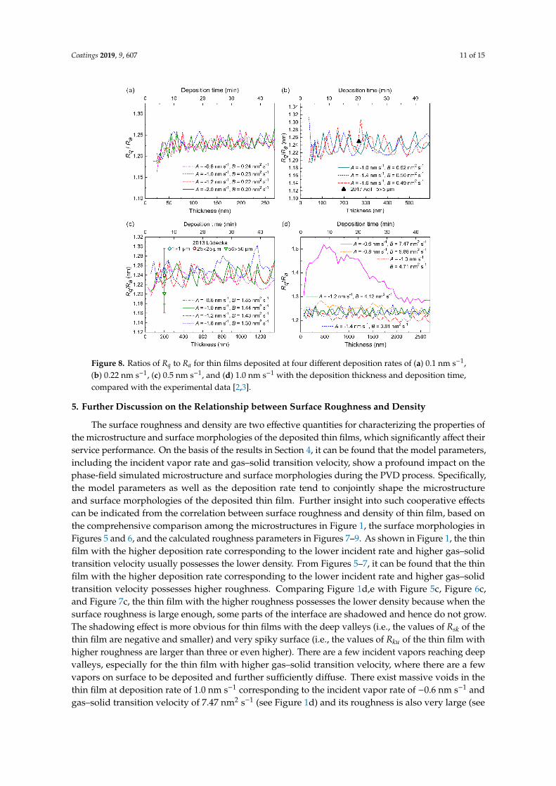
increase first as the deposited thickness and deposition time increase and then reach a steady state atthe thickness of about 50 nm. The values of Ra and Rq of the thin films with larger deposition ratesreach the steady state earlier than those with lower deposition rates, as confirmed in Figures 5 and 6.Moreover, the values of Ra and Rq of thin films tend to increase as the deposition rate increases at thesame incident vapor rate, whereas their values tend to decrease as the incident vapor rate increasefor the same deposition rate. Figure 8 shows the ratio of Rq to Ra for thin films deposited at fourdifferent deposition rates of 0.1, 0.22, 0.5, and 1.0 nm s−1 with the deposition thickness and depositiontime and also the comparison between ratios of Rq to Ra in the thin films with deposition rates of0.22 and 1.0 nm s−1 due to the phase-field simulations and the experimental data in Mo and Ti thinfilms [2,3]. From Figure 8, it is found that most of the calculated ratios of Rq to Ra approach 1.31,suggesting that the distributions of surface heights approach a Gaussian distribution, which is in
Coatings 2019, 9, 607 9 of 15
accordance with the report of Ref. [40]. Furthermore, the calculated ratios of Rq to Ra of thin filmswith deposition rates of 0.22 and 1.0 nm s−1 respectively agree well with the experimental data in Mothin film by Aqil et al. [2] and Ti thin film by Lüdecke et al. [3]. Figure 9 exhibits the values of Rskand Rku for thin films deposited at three different deposition rates of 0.1, 0.5, and 1.0 nm s−1 with thedeposition thickness and deposition time. From Figure 9, it can be seen that most of the values of Rskare negative, which indicates the valleys of most thin films due to the phase-field simulations, aredominant in the distribution. The values of Rsk of the thin film with the deposition rate of 1.0 nm s−1,corresponding to the incident rate of −0.6 nm s−1 and gas–solid transition velocity of 7.47 nm2 s−1, arenegative and much smaller than the others, which indicates that there are a lot of very deep valleysin this thin film. The values of Rku of the thin films, except for the thin film with the deposition rateof 1.0 nm s−1, corresponding to the incident rate of −0.6 nm s−1 and gas–solid transition velocity of7.47 nm2 s−1 due to the phase-field simulation are smaller than 3, indicating their surfaces are bumpy.The values of Rku of the thin film with the deposition rate of 1.0 nm s−1 corresponding to the incidentrate of −0.6 nm s–1 and gas–solid transition velocity of 7.47 nm2 s−1 are larger than 3, indicating itssurface is spiky. As shown in Figures 7–9, there are apparent differences in the calculated roughnessparameters between the thin film with the deposition rate of 1.0 nm s−1 corresponding to the incidentrate of −0.6 nm s−1 and gas–solid transition velocity of 7.47 nm2 s−1 and the others. That is becausethe valleys of the surface in the thin film with the deposition rate of 1.0 nm s−1 corresponding to theincident rate of −0.6 nm s−1 and gas–solid transition velocity of 7.47 nm2 s−1 are very deep and theirpeaks are quite spiky because of the well-known shadow effects. Such deep valleys of the surface inthe thin film will evolve to voids as the deposition time increases.
Coatings 2019, 9, x FOR PEER REVIEW 8 of 15
Figure 5. Heat maps of the surface height of thin films deposited with three different deposition rates corresponding to the incident vapor rate fixed as −0.6 nm s−1 and three different gas-solid transition velocities at three different deposition time of 5, 20 and 35 min due to the phase-field simulations.
Figure 6. Heat maps of the surface height of thin films deposited with three different deposition rates corresponding to the incident vapor rate fixed as −1.0 nm s−1 and three different gas-solid transition velocities at three different deposition time of 5, 20 and 35 min due to the phase-field simulations.
Figure 6. Heat maps of the surface height of thin films deposited with three different deposition ratescorresponding to the incident vapor rate fixed as −1.0 nm s−1 and three different gas-solid transitionvelocities at three different deposition time of 5, 20 and 35 min due to the phase-field simulations.
Coatings 2019, 9, 607 10 of 15
Coatings 2019, 9, x FOR PEER REVIEW 10 of 15
Figure 7. Values of Ra and Rq for thin films deposited at three different deposition rates of (a) 0.1 nm s−1, (b) 0.5 nm s−1, and (c) 1.0 nm s−1 with the corresponding deposition thickness and time. Figure 7. Values of Ra and Rq for thin films deposited at three different deposition rates of (a) 0.1 nm s−1,(b) 0.5 nm s−1, and (c) 1.0 nm s−1 with the corresponding deposition thickness and time.
Coatings 2019, 9, 607 11 of 15
Coatings 2019, 9, x FOR PEER REVIEW 11 of 15
Figure 8. Ratios of Rq to Ra for thin films deposited at four different deposition rates of (a) 0.1 nm s−1, (b) 0.22 nm s−1, (c) 0.5 nm s−1, and (d) 1.0 nm s−1 with the deposition thickness and deposition time, compared with the experimental data [2,3].
5. Further Discussion on the Relationship between Surface Roughness and Density
The surface roughness and density are two effective quantities for characterizing the properties of the microstructure and surface morphologies of the deposited thin films, which significantly affect their service performance. On the basis of the results in Section 4, it can be found that the model parameters, including the incident vapor rate and gas–solid transition velocity, show a profound impact on the phase-field simulated microstructure and surface morphologies during the PVD process. Specifically, the model parameters as well as the deposition rate tend to conjointly shape the microstructure and surface morphologies of the deposited thin film. Further insight into such cooperative effects can be indicated from the correlation between surface roughness and density of thin film, based on the comprehensive comparison among the microstructures in Figure 1, the surface morphologies in Figures 5 and 6, and the calculated roughness parameters in Figures 7–9. As shown in Figure 1, the thin film with the higher deposition rate corresponding to the lower incident rate and higher gas–solid transition velocity usually possesses the lower density. From Figures 5–7, it can be found that the thin film with the higher deposition rate corresponding to the lower incident rate and higher gas–solid transition velocity possesses higher roughness. Comparing Figures 1d and e with Figures 5c, 6c, and 7c, the thin film with the higher roughness possesses the lower density because when the surface roughness is large enough, some parts of the interface are shadowed and hence do not grow. The shadowing effect is more obvious for thin films with the deep valleys (i.e., the values of Rsk of the thin film are negative and smaller) and very spiky surface (i.e., the values of Rku of the thin film with higher roughness are larger than three or even higher). There are a few incident vapors reaching deep valleys, especially for the thin film with higher gas–solid transition velocity, where there are a few vapors on surface to be deposited and further sufficiently diffuse. There exist massive voids in the thin film at deposition rate of 1.0 nm s−1 corresponding to the incident vapor rate of −0.6 nm s−1 and gas–solid transition velocity of 7.47 nm2 s−1 (see Figure 1d) and its roughness is also very large (see Figures 6c and 7c), which confirms the presently proposed relationship between the surface roughness and the density.
Figure 8. Ratios of Rq to Ra for thin films deposited at four different deposition rates of (a) 0.1 nm s−1,(b) 0.22 nm s−1, (c) 0.5 nm s−1, and (d) 1.0 nm s−1 with the deposition thickness and deposition time,compared with the experimental data [2,3].
5. Further Discussion on the Relationship between Surface Roughness and Density
The surface roughness and density are two effective quantities for characterizing the properties ofthe microstructure and surface morphologies of the deposited thin films, which significantly affect theirservice performance. On the basis of the results in Section 4, it can be found that the model parameters,including the incident vapor rate and gas–solid transition velocity, show a profound impact on thephase-field simulated microstructure and surface morphologies during the PVD process. Specifically,the model parameters as well as the deposition rate tend to conjointly shape the microstructureand surface morphologies of the deposited thin film. Further insight into such cooperative effectscan be indicated from the correlation between surface roughness and density of thin film, based onthe comprehensive comparison among the microstructures in Figure 1, the surface morphologies inFigures 5 and 6, and the calculated roughness parameters in Figures 7–9. As shown in Figure 1, the thinfilm with the higher deposition rate corresponding to the lower incident rate and higher gas–solidtransition velocity usually possesses the lower density. From Figures 5–7, it can be found that the thinfilm with the higher deposition rate corresponding to the lower incident rate and higher gas–solidtransition velocity possesses higher roughness. Comparing Figure 1d,e with Figure 5c, Figure 6c,and Figure 7c, the thin film with the higher roughness possesses the lower density because when thesurface roughness is large enough, some parts of the interface are shadowed and hence do not grow.The shadowing effect is more obvious for thin films with the deep valleys (i.e., the values of Rsk of thethin film are negative and smaller) and very spiky surface (i.e., the values of Rku of the thin film withhigher roughness are larger than three or even higher). There are a few incident vapors reaching deepvalleys, especially for the thin film with higher gas–solid transition velocity, where there are a fewvapors on surface to be deposited and further sufficiently diffuse. There exist massive voids in thethin film at deposition rate of 1.0 nm s−1 corresponding to the incident vapor rate of −0.6 nm s−1 andgas–solid transition velocity of 7.47 nm2 s−1 (see Figure 1d) and its roughness is also very large (see
Coatings 2019, 9, 607 12 of 15
Figures 6c and 7c), which confirms the presently proposed relationship between the surface roughnessand the density.Coatings 2019, 9, x FOR PEER REVIEW 12 of 15
Figure 9. Values of Rsk and Rku for thin films deposited at three different deposition rates of (a) 0.1 nm s−1, (b) 0.5 nm s−1, and (c) 1.0 nm s−1 with the corresponding deposition thickness and deposition time.
6. Conclusions
In this paper, more than 200 sets of 3D phase-field simulations of the PVD process of metal thin films were performed based on the parameterized phase-field model by Keblinski et al. A quantitative relationship between model parameters and deposition rates at steady state was established.
Insight into the relationship among the industrially concerned properties, i.e., deposition rates, surface roughness and density, and the microstructures and surface morphologies of the metal thin films was further investigated by conducting 3D phase-field simulations with larger domain. Relationship between the surface roughness and the deposition rate is proven to be in accordance with the common sense in experiments, i.e., that the higher deposition rate generally leads to the higher surface roughness. Specially, the calculated ratios of Rq to Ra of metal thin films with deposition rates of 0.22 and 1.0 nm s−1 are in very good agreement with the
Figure 9. Values of Rsk and Rku for thin films deposited at three different deposition rates of (a)0.1 nm s−1, (b) 0.5 nm s−1, and (c) 1.0 nm s−1 with the corresponding deposition thickness anddeposition time.
6. Conclusions
• In this paper, more than 200 sets of 3D phase-field simulations of the PVD process of metal thin filmswere performed based on the parameterized phase-field model by Keblinski et al. A quantitativerelationship between model parameters and deposition rates at steady state was established.
• Insight into the relationship among the industrially concerned properties, i.e., deposition rates,surface roughness and density, and the microstructures and surface morphologies of the metalthin films was further investigated by conducting 3D phase-field simulations with larger domain.Relationship between the surface roughness and the deposition rate is proven to be in accordance
Coatings 2019, 9, 607 13 of 15
with the common sense in experiments, i.e., that the higher deposition rate generally leads tothe higher surface roughness. Specially, the calculated ratios of Rq to Ra of metal thin films withdeposition rates of 0.22 and 1.0 nm s−1 are in very good agreement with the experimental data ofthe deposited Mo and Ti thin films.
• Delicate elaboration over the formation of voids and the relation between the density androughness was acquired by carefully associating the relation among different control parameters.It was found that the metal thin films with the higher roughness usually possess the lower density.Furthermore, the present results reveal the potential difficulties in the PVD process as the controlparameters tend to affect the properties of thin films conjointly.
• With the present quantitative phase-field simulations, the relationship between the controlparameters and microstructures and properties of the deposited thin films can be efficientlyestablished, which is anticipated to be used for precisely guiding the manufacture of thin filmswith the desired properties by means of the PVD technique.
Author Contributions: Conceptualization, L.Z. and M.C.; methodology and code, S.Y. and J.Z.; validation, S.Y.,J.Z., and L.Z.; writing—original draft preparation, S.Y. and J.Z.; writing—review and editing, J.Z. and L.Z.; projectadministration, M.C. and L.Z.
Funding: This research was funded by the National MCF Energy R & D Program of China, grant number2018YFE0306100, and the Director Foundation of China Academy of Engineering Physics, grant number YZ2015009.
Conflicts of Interest: The authors declare no conflict of interest.
References
1. Chan, K.Y.; Tou, T.Y.; Teo, B.-S. Effects of substrate temperature on electrical and structural properties ofcopper thin films. Microelectron. J. 2006, 37, 930–937. [CrossRef]
2. Aqil, M.M.; Azam, M.A.; Aziz, M.F.; Latif, R. Deposition and characterization of molybdenum thin filmusing direct current magnetron and atomic force microscopy. J. Nanotechnol. 2017, 2017, 4862087. [CrossRef]
3. Lüdecke, C.; Bossert, J.; Roth, M.; Jandt, K.D. Physical vapor deposited titanium thin films forbiomedical applications: Reproducibility of nanoscale surface roughness and microbial adhesion properties.Appl. Surf. Sci. 2013, 280, 578–589. [CrossRef]
4. Singh, A.; Kuppusami, P.; Thirumurugesan, R.; Ramaseshan, R.; Kamruddin, M.; Dash, S.; Ganesan, V.;Mohandas, E. Study of microstructure and nanomechanical properties of Zr films prepared by pulsedmagnetron sputtering. Appl. Surf. Sci. 2011, 257, 9909–9914. [CrossRef]
5. Li, C.; Guo, H.; Gao, L.; Wei, L.; Gong, S.; Xu, H. Microstructures of yttria-stabilized zirconia coatings byplasma spray-physical vapor deposition. J. Therm. Spray Technol. 2015, 24, 534–541. [CrossRef]
6. Ta, N.; Zhang, L.; Tang, Y.; Chen, W.; Du, Y. Effect of temperature gradient on microstructure evolutionin Ni–Al–Cr bond coat/substrate systems: A phase-field study. Surf. Coat. Technol. 2015, 261, 364–374.[CrossRef]
7. Ta, N.; Zhang, L.; Du, Y. A trial to design γ/γ′ bond coat in Ni–Al–Cr Mode TBCs Aided by Phase-FieldSimulation. Coatings 2018, 8, 421. [CrossRef]
9. Grigoriev, S.; Vereschaka, A.; Metel, A.; Sitnikov, N.; Milovich, F.; Andreev, N.; Shevchenko, S.; Rozhkova, Y.Investigation into Performance of multilayer composite nano-structured Cr-CrN-(Cr0.35Ti0.40Al0.25) Ncoating for metal cutting tools. Coatings 2018, 8, 447. [CrossRef]
10. Bujak, J.; Walkowicz, J.; Kusinski, J. Influence of the nitrogen pressure on the structure and properties of(Ti, Al) N coatings deposited by cathodic vacuum arc PVD process. Surf. Coat. Technol. 2004, 180, 150–157.[CrossRef]
11. Kazmanli, M.; Ürgen, M.; Cakir, A. Effect of nitrogen pressure, bias voltage and substrate temperature onthe phase structure of Mo–N coatings produced by cathodic arc PVD. Surf. Coat. Technol. 2003, 167, 77–82.[CrossRef]
12. Ahlgren, M.; Blomqvist, H. Influence of bias variation on residual stress and texture in TiAlN PVD coatings.Surf. Coat. Technol. 2005, 200, 157–160. [CrossRef]
13. Sprute, T.; Tillmann, W.; Grisales, D.; Selvadurai, U.; Fischer, G. Influence of substrate pre-treatments onresidual stresses and tribo-mechanical properties of TiAlN-based PVD coatings. Surf. Coat. Technol. 2014,260, 369–379. [CrossRef]
14. Nastac, L.; Dong, H.; Dax, F.R.; Hanusiak, W. The CFD modeling of the EB-PVD of SiC/Ti-6Al-4V coatings.JOM 2004, 56, 49–53. [CrossRef]
15. Adebiyi, D.; Popoola, A.; Botef, I. Experimental verification of statistically optimized parameters forlow-pressure cold spray coating of titanium. Metals 2016, 6, 135. [CrossRef]
16. Kapopara, J.M.; Mengar, A.R.; Chauhan, K.V.; Rawal, S.K. CFD analysis of sputtered TiN coating. Mater.Today Proc. 2017, 4, 9390–9393. [CrossRef]
18. Raghavan, S.; Mayo, M.J.; Wang, H.; Dinwiddie, R.B.; Porter, W.D. The effect of grain size, porosity and yttriacontent on the thermal conductivity of nanocrystalline zirconia. Scr. Mater. 1998, 39, 1119–1125. [CrossRef]
19. Mayrhofer, P.H.; Tischler, G.; Mitterer, C. Microstructure and mechanical/thermal properties of Cr–N coatingsdeposited by reactive unbalanced magnetron sputtering. Surf. Coat. Technol. 2001, 142, 78–84. [CrossRef]
20. Kulkarni, A.; Vaidya, A.; Goland, A.; Sampath, S.; Herman, H. Processing effects on porosity-propertycorrelations in plasma sprayed yttria-stabilized zirconia coatings. Mater. Sci. Eng. A 2003, 359, 100–111.[CrossRef]
21. Mayrhofer, P.; Mitterer, C.; Musil, J. Structure–property relationships in single-and dual-phase nanocrystallinehard coatings. Surf. Coat. Technol. 2003, 174, 725–731.
22. Zhang, C.X.; Liu, F.S.; Gong, S.K.; Xu, H.B. Characterization and evaluation of EB-PVD thermal barriercoatings by impedance spectroscopy. Mater. Sci. Forum 2005, 475–479, 3997–4000.
23. Jang, B.-K.; Matsubara, H. Influence of porosity on thermophysical properties of nano-porous zirconiacoatings grown by electron beam-physical vapor deposition. Scr. Mater. 2006, 54, 1655–1659. [CrossRef]
24. Sohn, Y.; Biederman, R.; Sisson, R., Jr. Microstructural development in physical vapour-deposited partiallystabilized zirconia thermal barrier coatings. Thin Solid Films 1994, 250, 1–7.
25. Schulz, U.; Schmücker, M. Microstructure of ZrO2 thermal barrier coatings applied by EB-PVD. Mater. Sci.Eng. A 2000, 276, 1–8. [CrossRef]
26. Yang, Y.; Johnson, R.; Wadley, H. A Monte Carlo simulation of the physical vapor deposition of nickel.Acta Mater. 1997, 45, 1455–1468.
27. Zhang, J.; Adams, J.B. Modeling and visualization of polycrystalline thin film growth. Comput. Mater. Sci.2004, 31, 317–328. [CrossRef]
28. Cho, J.; Terry, S.; LeSar, R.; Levi, C. A kinetic Monte Carlo simulation of film growth by physical vapordeposition on rotating substrates. Mater. Sci. Eng. A 2005, 391, 390–401. [CrossRef]
29. Wang, P.; He, W.; Mauer, G.; Mücke, R.; Vaßen, R. Monte Carlo simulation of column growth in plasma sprayphysical vapor deposition process. Surf. Coat. Technol. 2018, 335, 188–197. [CrossRef]
30. Wang, Z.; Zhang, D.; Ke, P.; Liu, X.; Wang, A. Influence of substrate negative bias on structure and propertiesof TiN coatings prepared by hybrid HIPIMS method. J. Mater. Sci. Technol. 2015, 31, 37–42.
31. Raoufi, D.; Kiasatpour, A.; Fallah, H.R.; Rozatian, A.S.H. Surface characterization and microstructure of ITOthin films at different annealing temperatures. Appl. Surf. Sci. 2007, 253, 9085–9090. [CrossRef]
32. Huang, Y.; Lü, X.; Jing, W.M.; Huang, N. In vitro investigation of protein adsorption and platelet adhesionon inorganic biomaterial surfaces. Appl. Surf. Sci. 2008, 255, 257–259. [CrossRef]
33. Puckett, S.D.; Taylor, E.; Raimondo, T.; Webster, T.J. The relationship between the nanostructure of titaniumsurfaces and bacterial attachment. Biomaterials 2010, 31, 706–713. [CrossRef] [PubMed]
34. Keblinski, P.; Maritan, A.; Toigo, F.; Messier, R.; Banavar, J.R. Continuum model for the growth of interfaces.Phys. Rev. E 1996, 53, 759. [CrossRef] [PubMed]
37. Stewart, J.A.; Spearot, D.E. Phase-field simulations of microstructure evolution during physical vapordeposition of single-phase thin films. Comput. Mater. Sci. 2017, 131, 170–177. [CrossRef]
38. Bhushan, B. Surface roughness analysis and measurement techniques. In Modern Tribology Handbook, TwoVolume Set, 1st ed.; CRC press: Boca Raton, FL, USA, 2000; pp. 79–150.
39. Kumar, B.R.; Rao, T.S. AFM Studies on surface morphology, topography and texture of nanostructured zincaluminum oxide thin films. Dig. J. Nanomater. Bios. 2012, 7, 1881–1889.
40. Thomas, T.R. Rough Surfaces, 2nd ed.; Imperial College Press: London, UK, 1999; pp. 133–150.