Lecture Notes in Electrical Engineering 183 A Practical Design of Lumped, Semi-lumped & Microwave Cavity Filters Bearbeitet von Dhanasekharan Natarajan 1. Auflage 2012. Buch. xii, 148 S. Hardcover ISBN 978 3 642 32860 2 Format (B x L): 15,5 x 23,5 cm Gewicht: 409 g Weitere Fachgebiete > Technik > Elektronik > Mikrowellentechnik Zu Inhaltsverzeichnis schnell und portofrei erhältlich bei Die Online-Fachbuchhandlung beck-shop.de ist spezialisiert auf Fachbücher, insbesondere Recht, Steuern und Wirtschaft. Im Sortiment finden Sie alle Medien (Bücher, Zeitschriften, CDs, eBooks, etc.) aller Verlage. Ergänzt wird das Programm durch Services wie Neuerscheinungsdienst oder Zusammenstellungen von Büchern zu Sonderpreisen. Der Shop führt mehr als 8 Millionen Produkte.
Transcript
Lecture Notes in Electrical Engineering 183
A Practical Design of Lumped, Semi-lumped & Microwave Cavity Filters
Weitere Fachgebiete > Technik > Elektronik > Mikrowellentechnik
Zu Inhaltsverzeichnis
schnell und portofrei erhältlich bei
Die Online-Fachbuchhandlung beck-shop.de ist spezialisiert auf Fachbücher, insbesondere Recht, Steuern und Wirtschaft.Im Sortiment finden Sie alle Medien (Bücher, Zeitschriften, CDs, eBooks, etc.) aller Verlage. Ergänzt wird das Programmdurch Services wie Neuerscheinungsdienst oder Zusammenstellungen von Büchern zu Sonderpreisen. Der Shop führt mehr
Abstract Impedance, Characteristic impedance, RF transmission line and VSWRare fundamental terms not only for the design of RF filters but also for all RFcomponents and circuits. The terms are explained in detail with simple examplesfor physical understanding. Impedance is explained for a discrete reactive elementcircuit and for a single load resistor introducing the concept of distributed reactiveelements. The construction and characteristics of coaxial, microstrip and striplinetransmission lines are explained. VSWR is explained graphically with numericalexamples for transmission line with open-circuited load, short-circuited load,matched load, infinitely long coaxial cable and partially matched load afterexplaining its practical significance.
2.1 Introduction
RF filters are designed as per customer requirements. The requirements varyamong the four basic types (low pass, high pass, band pass and band stop) of filters.However, all the four types of filters have a few requirements in common. RFfilters are designed for the standardised input/output characteristic impedance,50 X. RF transmission lines are used in the design of microwave filters. Input andoutput VSWR of filters are measured to verify compliance to the specified char-acteristic impedance and to ensure minimum insertion loss. Impedance, Charac-teristic impedance, RF transmission lines and VSWR are fundamental terms notonly for the design of RF filters but also for all RF components and circuits. Hence,the terms are explained in detail with examples. The other filter terms such asInsertion loss, Band width and Rejection represent the characteristics of filters andthey are explained in Chap. 3.
D. Natarajan, A Practical Design of Lumped, Semi-Lumped and MicrowaveCavity Filters, Lecture Notes in Electrical Engineering,DOI: 10.1007/978-3-642-32861-9_2, � Springer-Verlag Berlin Heidelberg 2013
7
2.2 Impedance
2.2.1 Definition
Resistance (R) is defined as the measure of the opposition to direct current (DC) oralternating current (AC) assuming that the resistance is pure in the sense that itdoes not have inductive or capacitive reactance. It is expressed in ohms.
Impedance (Z) is analogous to resistance and is defined as the measure of theopposition to the flow of alternating current. Resistance (R) and reactance (X) arepart of impedance. Reactance may be due to inductance or capacitance or both. Itis expressed in ohms.
Z ¼ pðR2 þ X2Þ
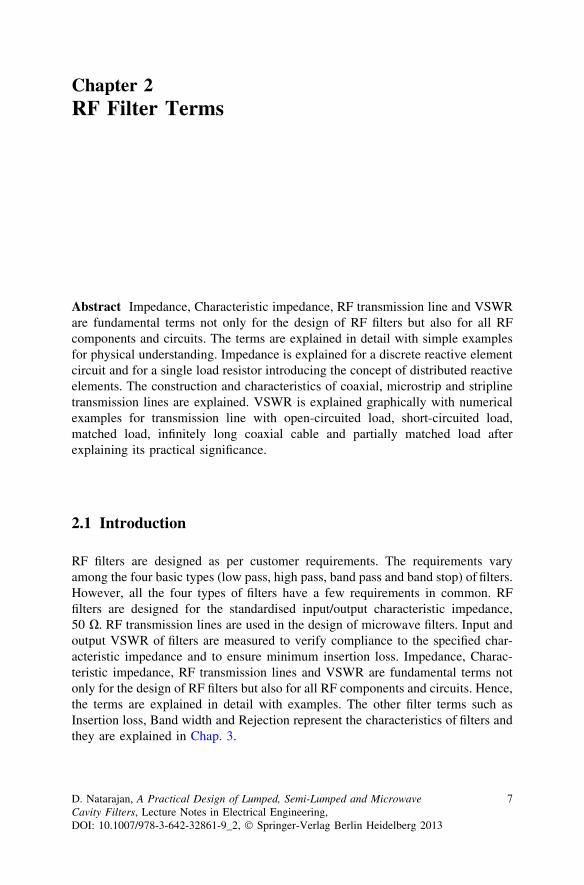
If X = 0, the impedance is said to be resistive. At lower frequencies, imped-ance is relevant for a discrete circuit having resistors, inductors and capacitorsconnected in series/parallel configuration. A 4-element discrete circuit withcapacitors and inductors is shown in Fig. 2.1. The impedance of the circuit iscalculated using appropriate expressions for the series/parallel configuration.
2.2.2 Load Resistor at Radio Frequency
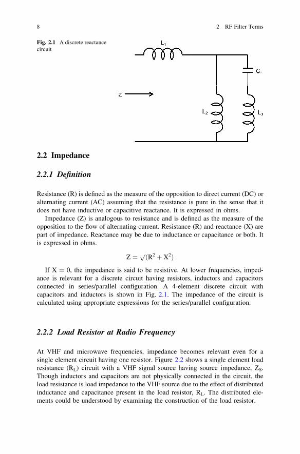
At VHF and microwave frequencies, impedance becomes relevant even for asingle element circuit having one resistor. Figure 2.2 shows a single element loadresistance (RL) circuit with a VHF signal source having source impedance, ZS.Though inductors and capacitors are not physically connected in the circuit, theload resistance is load impedance to the VHF source due to the effect of distributedinductance and capacitance present in the load resistor, RL. The distributed ele-ments could be understood by examining the construction of the load resistor.
Fig. 2.1 A discrete reactancecircuit
8 2 RF Filter Terms
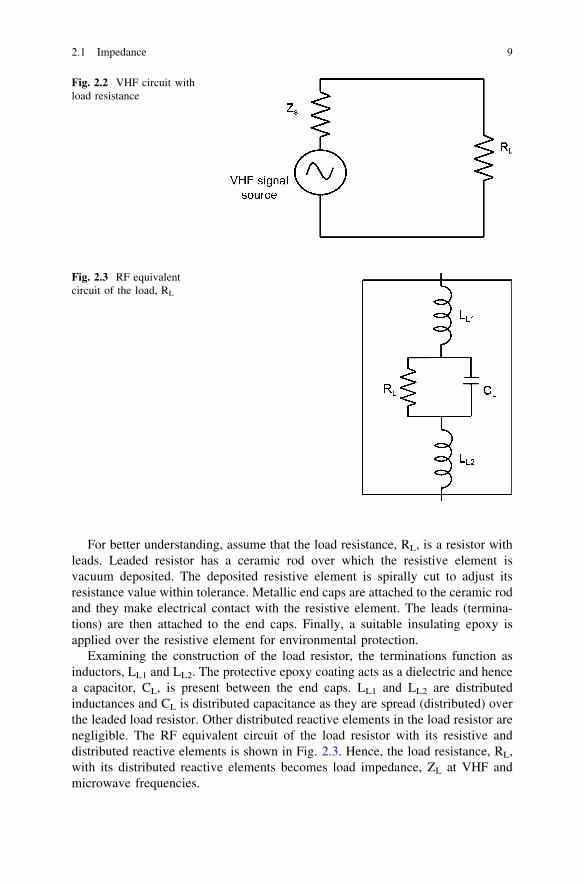
For better understanding, assume that the load resistance, RL, is a resistor withleads. Leaded resistor has a ceramic rod over which the resistive element isvacuum deposited. The deposited resistive element is spirally cut to adjust itsresistance value within tolerance. Metallic end caps are attached to the ceramic rodand they make electrical contact with the resistive element. The leads (termina-tions) are then attached to the end caps. Finally, a suitable insulating epoxy isapplied over the resistive element for environmental protection.
Examining the construction of the load resistor, the terminations function asinductors, LL1 and LL2. The protective epoxy coating acts as a dielectric and hencea capacitor, CL, is present between the end caps. LL1 and LL2 are distributedinductances and CL is distributed capacitance as they are spread (distributed) overthe leaded load resistor. Other distributed reactive elements in the load resistor arenegligible. The RF equivalent circuit of the load resistor with its resistive anddistributed reactive elements is shown in Fig. 2.3. Hence, the load resistance, RL,with its distributed reactive elements becomes load impedance, ZL at VHF andmicrowave frequencies.
Fig. 2.2 VHF circuit withload resistance
Fig. 2.3 RF equivalentcircuit of the load, RL
2.1 Impedance 9
2.2.3 Standard Terminations
For the performance verification of RF components such as filters, the input of thecomponent is connected to RF source and the output is terminated with resistiveload impedance. Load impedances are standardised to 75 and 50 X. Standardtermination is a commercial terminology for the standardised loads. The termi-nations are specially designed coaxial film resistors minimising distributedcapacitance and inductance. They are available in BNC, TNC, N, SMA and otherconnector series. The terminations are used for the initial set up calibration of RFtest equipments. The frequency of application is generally limited to 1 GHz for75 X terminations whereas 50 X terminations are used up to microwavefrequencies.
The concept of minimising distributed inductance and capacitance is used todesign resistive termination at microwave frequencies by cancelling inductivereactance with capacitive reactance at that frequency using reactive matchingnetworks [1].
2.3 RF Transmission Line
2.3.1 Definition
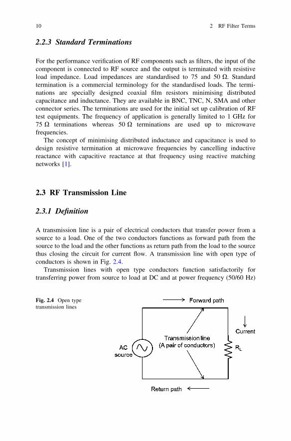
A transmission line is a pair of electrical conductors that transfer power from asource to a load. One of the two conductors functions as forward path from thesource to the load and the other functions as return path from the load to the sourcethus closing the circuit for current flow. A transmission line with open type ofconductors is shown in Fig. 2.4.
Transmission lines with open type conductors function satisfactorily fortransferring power from source to load at DC and at power frequency (50/60 Hz)
Fig. 2.4 Open typetransmission lines
10 2 RF Filter Terms
or up to 100 kHz with acceptable degradation. However, the open transmissionlines are not acceptable at radio frequency as it will result in the loss of RF signalswhen transferring power from source to load. RF signals are electromagneticwaves and they propagate through a dielectric medium including free space andvacuum. A specially designed structure having a dielectric medium contained byelectrically conducting walls is required for the propagation of electromagneticwaves to minimise the loss of RF signals. The specially designed structure is RFtransmission line. Many designs of transmission lines are available consideringfrequency, loss and other interconnection requirements of applications.
2.3.2 Types of Transmission Lines
The RF transmission line structures that find wide applications are:
Feeder cables to antennas and interconnection cables between RF sub-systemsare some of the applications of coaxial cables. Microstrip and stripline lines findapplications in the design of filters and other RF components. The construction andcharacteristics of coaxial and microstrip/stripline transmission lines are explained.Waveguides are special form of transmission lines and they are used at microwavefrequencies.
2.4 Coaxial Transmission Lines
2.4.1 Construction and Characteristics
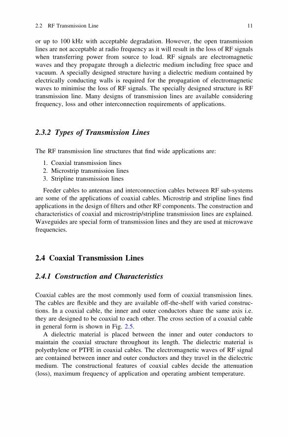
Coaxial cables are the most commonly used form of coaxial transmission lines.The cables are flexible and they are available off-the-shelf with varied construc-tions. In a coaxial cable, the inner and outer conductors share the same axis i.e.they are designed to be coaxial to each other. The cross section of a coaxial cablein general form is shown in Fig. 2.5.
A dielectric material is placed between the inner and outer conductors tomaintain the coaxial structure throughout its length. The dielectric material ispolyethylene or PTFE in coaxial cables. The electromagnetic waves of RF signalare contained between inner and outer conductors and they travel in the dielectricmedium. The constructional features of coaxial cables decide the attenuation(loss), maximum frequency of application and operating ambient temperature.
2.2 RF Transmission Line 11
The dielectric material of coaxial cables contributes significantly for the loss ofthe cables. Air bubbles are injected during the manufacture of polyethylene orPFFE dielectric material and the air-foamed dielectric cables have lower loss.Selecting coaxial cables with higher diameter or with silver plated inner/outerconductors reduces the loss of the cables further. Coaxial cable is available withouter conductor braided with many strands of copper wires or with seamlesscopper tube. Coaxial cables with seamless copper tube outer conductor and PTFEdielectric are semi-rigid cables and they are suitable for applications up to 20 GHz.The maximum operating ambient temperature is 85 �C for cables with polyeth-ylene dielectric and is 180 �C for PTFE dielectric cables.
TEM (Transverse Electro-Magnetic) mode is the dominant mode of propaga-tion in RF coaxial cables. The propagation modes of transmission is brieflyexplained in Appendix-1. TEM mode in coaxial cables changes to higher ordermodes at a frequency called cut-off frequency, resulting in very high attenuationand hence the operating frequency of coaxial cables should be lower than the cut-off frequency. The expression published by leading international cable manufac-turers is useful to estimate the cut-off frequency, fc, of a coaxial cable.
fc GHzð Þ � 191=½ðDþ dÞ ðperÞ�
D Inner diameter of outer conductor in mmd Outer diameter of inner conductor in mmer is the relative dielectric constant of the medium between the conductors
2.4.2 Standard Coaxial Air Lines
RF coaxial transmission lines with air as dielectric are Standard air lines. Standardair line has rigid silver plated inner and outer conductors which are connected toprecision 7 or 3.5 mm coaxial connectors on both sides. The centre conductor ofstandard air line is mechanically supported by the centre conductors of the end
Fig. 2.5 Cross section of acoaxial cable
12 2 RF Filter Terms
coaxial connectors. Standard air lines are characterised by the lowest loss permeter and VSWR. They are used as standards for impedance measurements.
2.5 Microstrip/Stripline Transmission Lines
Microstrip or stripline transmission line patterns are designed and printed on PTFEcopper clad laminate. The laminate is a sheet of PTFE insulating material (sub-strate) bonded with copper sheet on both sides. Transmission line patterns printedon the laminate by special chemical etching processes. The unwanted copper isetched out on both sides of substrate by the chemical processes. Copper conductor(transmission line) width, thickness of substrate and the dielectric constant of thesubstrate decide the ‘characteristic impedance’ of microstrip or stripline trans-mission lines. Characteristic impedance and the applications of basic microstripand stripline configurations are explained in Chap. 4. Advanced filler materials areadded to the PTFE substrate for improving the stability and Q-factor of PTFEcopper clad laminate. For HF and VHF applications, glass epoxy copper cladsheets is also used for designing RF components in microstrip and striplineconfigurations.
2.6 Characteristic Impedance
Characteristic impedance is explained for coaxial transmission line. The crosssection of a coaxial cable shown in Fig. 2.5 is referred for explaining the char-acteristic impedance of a coaxial transmission line. Assume that the length ofcoaxial cable is infinite or long enough to act as load impedance. The inner andouter conductors have series distributed inductance. Distributed capacitance ispresent across the conductors throughout the length of the coaxial cable. The cablehas also series DC resistance and shunt conductance but their contributions for theinput impedance of the cable are considered negligible compared to the reactanceat high frequencies. The input impedance of the cable is given by the expression,H(L/C), where L is the distributed inductance and C is the distributed capacitanceper unit length of the coaxial cable [2]. The values of L and C are related to theparameters, D, d, and er, shown in Fig. 2.5. In other words, D, d and er distinctlydefines or characterises the input impedance of a coaxial cable. Hence, the char-acteristic impedance of a coaxial transmission line is defined as the inputimpedance of the line and is expressed in terms of D, d and er [3]. Its unit is ohmsand the symbol is Zo.
Characteristic impedance, Z0 ¼60 ln(D/d)
ffiffiffiffi
erp ohms
2.3 Coaxial Transmission Lines 13
Characteristic impedance of a coaxial cable is measured using Vector NetworkAnalyser with Time Domain Reflectometer (TDR) software. TDR equipment withStandard air line is also used for measuring the impedance. As the characteristicimpedance of a coaxial cable is related to its dimensions, the bending diameter ofthe cable should exceed 10 times the cable diameter during handling orapplications.
The loss (attenuation) of RF transmission lines is minimum at Zo = 77 X andthe power handling capacity of the lines is maximum at Zo = 30 X. Consideringlow loss requirements, characteristic impedance of 75 X is standardised for videoapplications. Characteristic impedance of 50 X is standardised for all otherapplications balancing loss and power handling requirements [4].
2.7 VSWR
2.7.1 Maximum Power Transfer
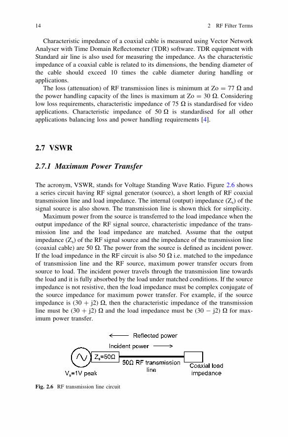
The acronym, VSWR, stands for Voltage Standing Wave Ratio. Figure 2.6 showsa series circuit having RF signal generator (source), a short length of RF coaxialtransmission line and load impedance. The internal (output) impedance (Zs) of thesignal source is also shown. The transmission line is shown thick for simplicity.
Maximum power from the source is transferred to the load impedance when theoutput impedance of the RF signal source, characteristic impedance of the trans-mission line and the load impedance are matched. Assume that the outputimpedance (Zs) of the RF signal source and the impedance of the transmission line(coaxial cable) are 50 X. The power from the source is defined as incident power.If the load impedance in the RF circuit is also 50 X i.e. matched to the impedanceof transmission line and the RF source, maximum power transfer occurs fromsource to load. The incident power travels through the transmission line towardsthe load and it is fully absorbed by the load under matched conditions. If the sourceimpedance is not resistive, then the load impedance must be complex conjugate ofthe source impedance for maximum power transfer. For example, if the sourceimpedance is (30 ? j2) X, then the characteristic impedance of the transmissionline must be (30 ? j2) X and the load impedance must be (30 - j2) X for max-imum power transfer.
Fig. 2.6 RF transmission line circuit
14 2 RF Filter Terms
If the load impedance is not matched to the impedance of RF circuit, somepercentage of the incident power is returned i.e. reflected by the load towards thesource through the transmission line. The quantum of the reflected power dependson the level of mismatch. If the load is open-circuit (load not connected to thetransmission line) or the load is short circuit, the incident power is totally reflectedat the end of the transmission line. The end of the transmission line is termed as theplane of the load. If the load impedance is partially matched (Ex: 40 or 60 X), thena fraction of the incident power is reflected back towards the source and theremaining power is absorbed by the load. The directions of incident power and thereflected power are shown in Fig. 2.6. Practical significance of VSWR is explainedwith an example.
2.7.2 Practical Significance of VSWR
Assume that a RF amplifier feeds an antenna through a RF coaxial feeder cable.The power amplifier is the RF source and the feeder cable is the transmission line.The antenna serves as the load impedance. Let the output impedance of the poweramplifier and the characteristic impedance of the feeder cable is 50 X. Let theimpedance of the antenna is 35 X, not matched to that of the source and the feedercable. Due to impedance mismatch, a portion of the incident power is reflected bythe antenna towards the amplifier and the remaining power is radiated. Thereflected power is dissipated in the power amplifier and the dissipation could resultin the premature (degradation) failure of the RF power transistor of the poweramplifier. Customers experience poor reception due to the radiation of less powerby the antenna. Hence, impedance matching is important for the satisfactoryperformance of RF systems. VSWR is a metric that measures how well theimpedances of various components are matched in RF circuits and systems torealise maximum power transfer. VSWR has no units as it is a ratio of voltages.
VSWR is explained for four cases of load impedance i.e. open circuit, shortcircuit, matched (50 X) and partially matched (Ex.: 40 or 60 X), assuming theoutput impedance of the RF signal source and the impedance of the transmissionline (coaxial cable) are 50 X. It is also assumed that the transmission line islossless and the source delivers a sinusoidal voltage, Vs, of 1 V peak at microwavefrequency, f (wave length, k).
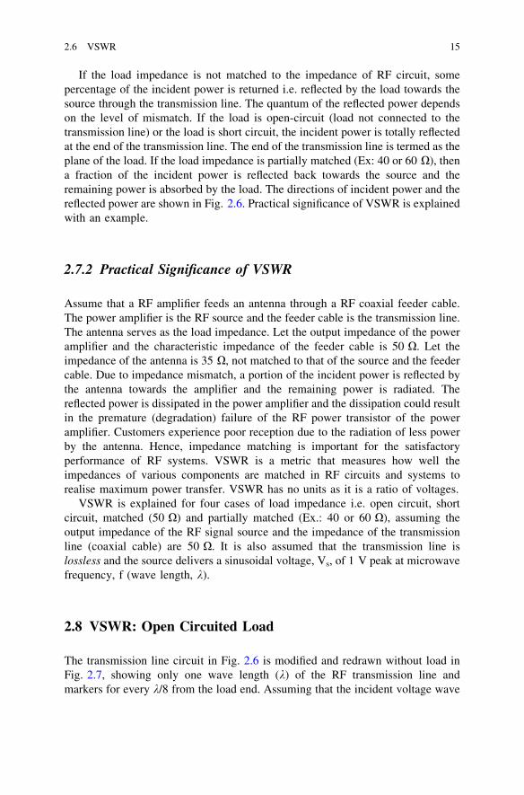
2.8 VSWR: Open Circuited Load
The transmission line circuit in Fig. 2.6 is modified and redrawn without load inFig. 2.7, showing only one wave length (k) of the RF transmission line andmarkers for every k/8 from the load end. Assuming that the incident voltage wave
2.6 VSWR 15
originates at a distance, k, from the load end, the analysis of incident and reflectedwaves is presented for one wave length.
2.8.1 Relationship Between Incident and Reflected Voltages
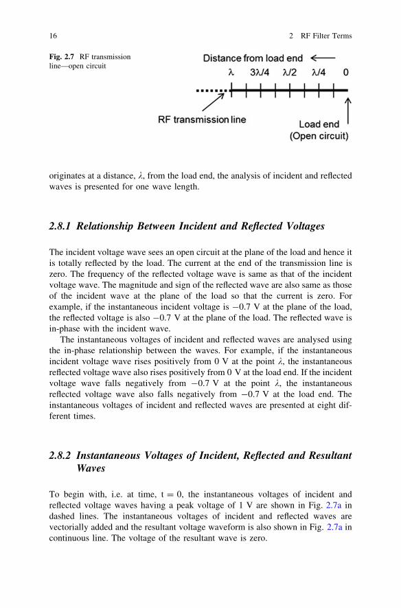
The incident voltage wave sees an open circuit at the plane of the load and hence itis totally reflected by the load. The current at the end of the transmission line iszero. The frequency of the reflected voltage wave is same as that of the incidentvoltage wave. The magnitude and sign of the reflected wave are also same as thoseof the incident wave at the plane of the load so that the current is zero. Forexample, if the instantaneous incident voltage is -0.7 V at the plane of the load,the reflected voltage is also -0.7 V at the plane of the load. The reflected wave isin-phase with the incident wave.
The instantaneous voltages of incident and reflected waves are analysed usingthe in-phase relationship between the waves. For example, if the instantaneousincident voltage wave rises positively from 0 V at the point k, the instantaneousreflected voltage wave also rises positively from 0 V at the load end. If the incidentvoltage wave falls negatively from -0.7 V at the point k, the instantaneousreflected voltage wave also falls negatively from -0.7 V at the load end. Theinstantaneous voltages of incident and reflected waves are presented at eight dif-ferent times.
2.8.2 Instantaneous Voltages of Incident, Reflected and ResultantWaves
To begin with, i.e. at time, t = 0, the instantaneous voltages of incident andreflected voltage waves having a peak voltage of 1 V are shown in Fig. 2.7a indashed lines. The instantaneous voltages of incident and reflected waves arevectorially added and the resultant voltage waveform is also shown in Fig. 2.7a incontinuous line. The voltage of the resultant wave is zero.
Fig. 2.7 RF transmissionline—open circuit
16 2 RF Filter Terms
At t = k/8, the incident voltage wave advances by k/8 towards the load and thereflected voltage wave also advances by k/8 towards the source. The wave formsof incident voltage, reflected voltage and the resultant voltage at t = k/8 are shownin Fig. 2.7b with the levels of instantaneous voltages. The peak voltage of theresultant voltage wave varies from -1.4 to +1.4 V.
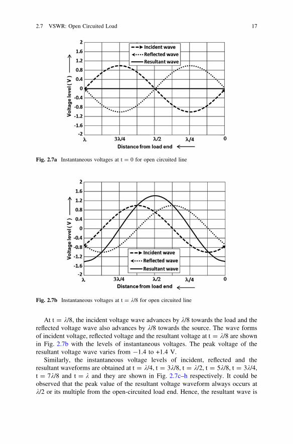
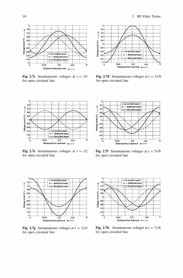
Similarly, the instantaneous voltage levels of incident, reflected and theresultant waveforms are obtained at t = k/4, t = 3k/8, t = k/2, t = 5k/8, t = 3k/4,t = 7k/8 and t = k and they are shown in Fig. 2.7c–h respectively. It could beobserved that the peak value of the resultant voltage waveform always occurs atk/2 or its multiple from the open-circuited load end. Hence, the resultant wave is
Fig. 2.7a Instantaneous voltages at t = 0 for open circuited line
Fig. 2.7b Instantaneous voltages at t = k/8 for open circuited line
2.7 VSWR: Open Circuited Load 17
Fig. 2.7c Instantaneous voltages at t = k/4for open circuited line
Fig. 2.7d Instantaneous voltages at t = 3k/8for open circuited line
Fig. 2.7e Instantaneous voltages at t = k/2for open circuited line
Fig. 2.7f Instantaneous voltages at t = 5k/8for open circuited line
Fig. 2.7g Instantaneous voltages at t = 3k/4for open circuited line
Fig. 2.7h Instantaneous voltages at t = 7k/8for open circuited line
18 2 RF Filter Terms
considered stationary i.e. standing. The peak voltage of the standing wave variesfrom -2 to +2 V.
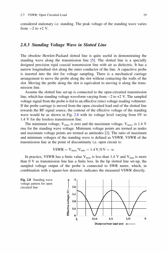
2.8.3 Standing Voltage Wave in Slotted Line
The obsolete Hewlett-Packard slotted line is quite useful in demonstrating thestanding wave along the transmission line [5]. The slotted line is a speciallydesigned precision rigid coaxial transmission line with air as dielectric. It has anarrow longitudinal slot along the outer conductor of the line. A capacitive probeis inserted into the slot for voltage sampling. There is a mechanical carriagearrangement to move the probe along the slot without contacting the walls of theslot. Moving the probe along the slot is equivalent to moving it along the trans-mission line.
Assume the slotted line set-up is connected to the open-circuited transmissionline, which has standing voltage waveform varying from -2 to +2 V. The sampledvoltage signal from the probe is fed to an effective (rms) voltage reading voltmeter.If the probe carriage is moved from the open circuited load end of the slotted linetowards the RF signal source, the contour of the effective voltage of the standingwave would be as shown in Fig. 2.8 with its voltage level varying from 0V to1.4 V for the lossless transmission line.
The minimum voltage, Vmin, is zero and the maximum voltage, Vmax, is 1.4 Vrms for the standing wave voltage. Minimum voltage points are termed as nodesand maximum voltage points are termed as antinodes [2]. The ratio of maximumand minimum voltages of the standing wave is defined as VSWR. VSWR of thetransmission line at the point of discontinuity i.e. open circuit is:
VSWR ¼ Vmax=Vmin ¼ 1:4 V=0 V ¼ 1
In practice, VSWR has a finite value Vmax is less than 1.4 V and Vmin is morethan 0 V as transmission line has a finite loss. In the hp slotted line set-up, thesampled voltage output of the probe is connected to SWR meter, which, incombination with a square-law detector, indicates the measured VSWR directly.
Fig. 2.8 Standing wavevoltage pattern for opencircuited line
2.7 VSWR: Open Circuited Load 19
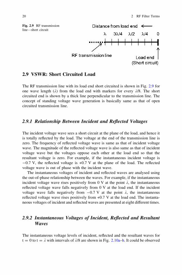
2.9 VSWR: Short Circuited Load
The RF transmission line with its load end short circuited is shown in Fig. 2.9 forone wave length (k) from the load end with markers for every k/8. The shortcircuited end is shown by a thick line perpendicular to the transmission line. Theconcept of standing voltage wave generation is basically same as that of opencircuited transmission line.
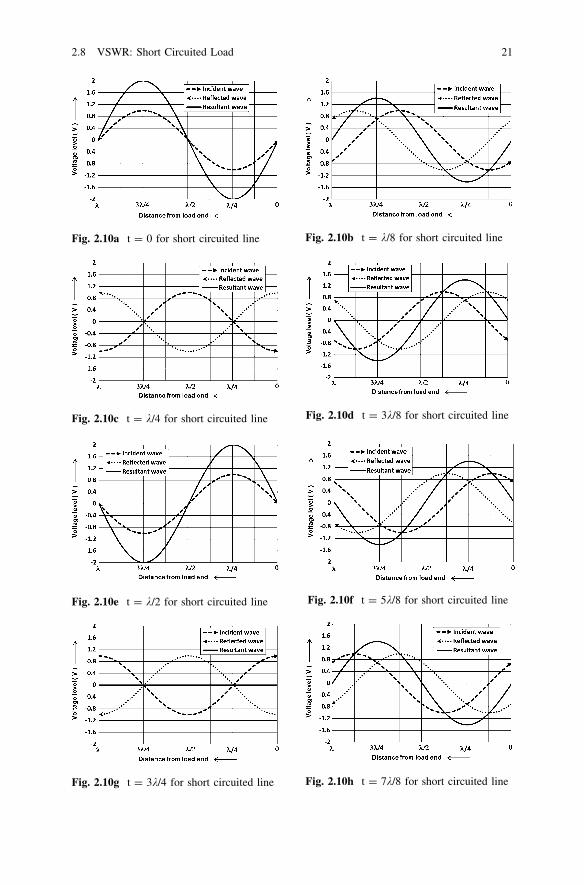
2.9.1 Relationship Between Incident and Reflected Voltages
The incident voltage wave sees a short circuit at the plane of the load, and hence itis totally reflected by the load. The voltage at the end of the transmission line iszero. The frequency of reflected voltage wave is same as that of incident voltagewave. The magnitude of the reflected voltage wave is also same as that of incidentvoltage wave but the voltages oppose each other at the load end so that theresultant voltage is zero. For example, if the instantaneous incident voltage is-0.7 V, the reflected voltage is +0.7 V at the plane of the load. The reflectedvoltage wave is out of phase with the incident wave.
The instantaneous voltages of incident and reflected waves are analysed usingthe out-of-phase relationship between the waves. For example, if the instantaneousincident voltage wave rises positively from 0 V at the point k, the instantaneousreflected voltage wave falls negatively from 0 V at the load end. If the incidentvoltage wave falls negatively from -0.7 V at the point k, the instantaneousreflected voltage wave rises positively from +0.7 V at the load end. The instanta-neous voltages of incident and reflected waves are presented at eight different times.
2.9.2 Instantaneous Voltages of Incident, Reflected and ResultantWaves
The instantaneous voltage levels of incident, reflected and the resultant waves fort = 0 to t = k with intervals of k/8 are shown in Fig. 2.10a–h. It could be observed
Fig. 2.9 RF transmissionline—short circuit
20 2 RF Filter Terms
Fig. 2.10a t = 0 for short circuited line
Fig. 2.10c t = k/4 for short circuited line
Fig. 2.10b t = k/8 for short circuited line
Fig. 2.10e t = k/2 for short circuited line Fig. 2.10f t = 5k/8 for short circuited line
Fig. 2.10d t = 3k/8 for short circuited line
Fig. 2.10g t = 3k/4 for short circuited line Fig. 2.10h t = 7k/8 for short circuited line
2.8 VSWR: Short Circuited Load 21
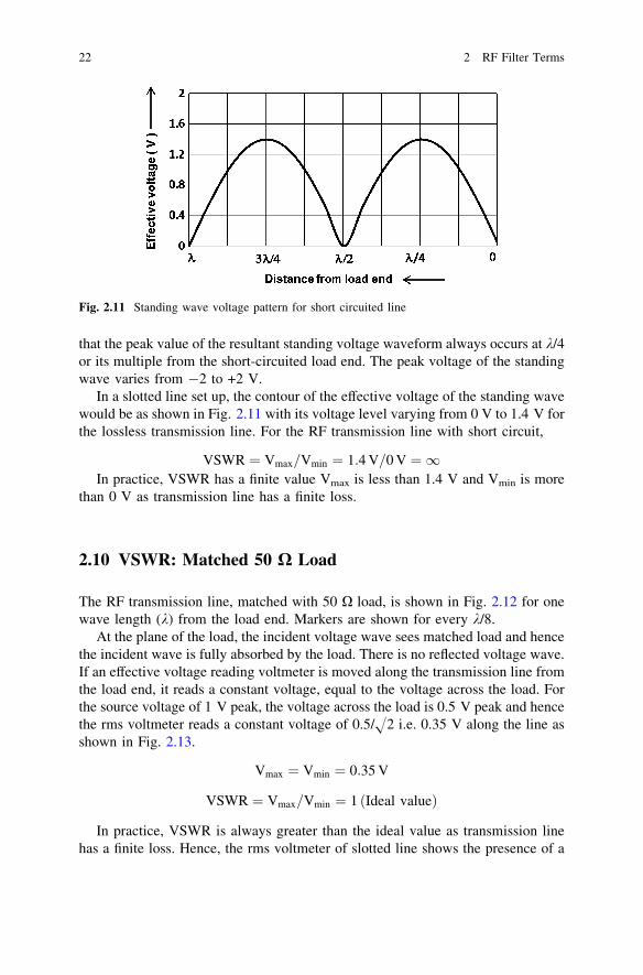
that the peak value of the resultant standing voltage waveform always occurs at k/4or its multiple from the short-circuited load end. The peak voltage of the standingwave varies from -2 to +2 V.
In a slotted line set up, the contour of the effective voltage of the standing wavewould be as shown in Fig. 2.11 with its voltage level varying from 0 V to 1.4 V forthe lossless transmission line. For the RF transmission line with short circuit,
VSWR ¼ Vmax=Vmin ¼ 1:4 V=0 V ¼ 1In practice, VSWR has a finite value Vmax is less than 1.4 V and Vmin is more
than 0 V as transmission line has a finite loss.
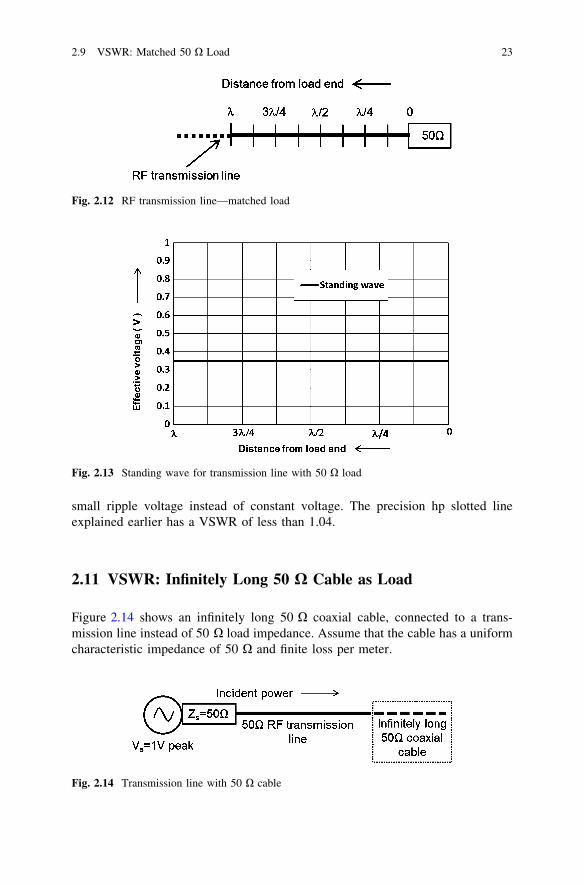
2.10 VSWR: Matched 50 X Load
The RF transmission line, matched with 50 X load, is shown in Fig. 2.12 for onewave length (k) from the load end. Markers are shown for every k/8.
At the plane of the load, the incident voltage wave sees matched load and hencethe incident wave is fully absorbed by the load. There is no reflected voltage wave.If an effective voltage reading voltmeter is moved along the transmission line fromthe load end, it reads a constant voltage, equal to the voltage across the load. Forthe source voltage of 1 V peak, the voltage across the load is 0.5 V peak and hencethe rms voltmeter reads a constant voltage of 0.5/H2 i.e. 0.35 V along the line asshown in Fig. 2.13.
Vmax ¼ Vmin ¼ 0:35 V
VSWR ¼ Vmax=Vmin ¼ 1 Ideal valueð Þ
In practice, VSWR is always greater than the ideal value as transmission linehas a finite loss. Hence, the rms voltmeter of slotted line shows the presence of a
Fig. 2.11 Standing wave voltage pattern for short circuited line
22 2 RF Filter Terms
small ripple voltage instead of constant voltage. The precision hp slotted lineexplained earlier has a VSWR of less than 1.04.
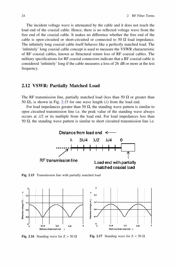
2.11 VSWR: Infinitely Long 50 X Cable as Load
Figure 2.14 shows an infinitely long 50 X coaxial cable, connected to a trans-mission line instead of 50 X load impedance. Assume that the cable has a uniformcharacteristic impedance of 50 X and finite loss per meter.
Fig. 2.12 RF transmission line—matched load
Fig. 2.13 Standing wave for transmission line with 50 X load
Fig. 2.14 Transmission line with 50 X cable
2.9 VSWR: Matched 50 X Load 23
The incident voltage wave is attenuated by the cable and it does not reach theload end of the coaxial cable. Hence, there is no reflected voltage wave from thefree end of the coaxial cable. It makes no difference whether the free end of thecable is open-circuited or short-circuited or connected to 50 X load impedance.The infinitely long coaxial cable itself behaves like a perfectly matched load. The‘infinitely’ long coaxial cable concept is used to measure the VSWR characteristicof RF coaxial cables, known as Structural return loss of RF coaxial cables. Themilitary specifications for RF coaxial connectors indicate that a RF coaxial cable isconsidered ‘infinitely’ long if the cable measures a loss of 26 dB or more at the testfrequency.
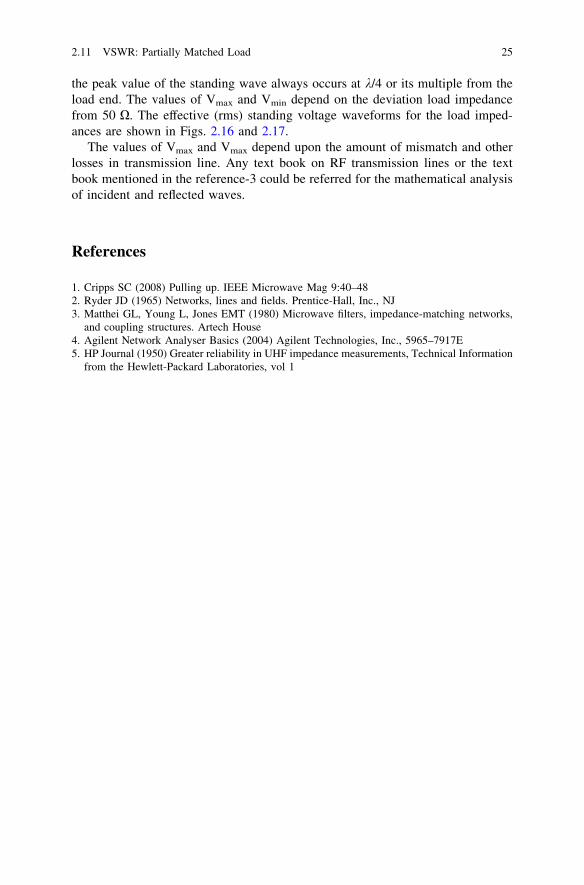
2.12 VSWR: Partially Matched Load
The RF transmission line, partially matched load (less than 50 X or greater than50 X), is shown in Fig. 2.15 for one wave length (k) from the load end.
For load impedances greater than 50 X, the standing wave pattern is similar toopen circuited transmission line i.e. the peak value of the standing wave alwaysoccurs at k/2 or its multiple from the load end. For load impedances less than50 X, the standing wave pattern is similar to short circuited transmission line i.e.
Fig. 2.15 Transmission line with partially matched load
Fig. 2.16 Standing wave for Z [ 50 X Fig. 2.17 Standing wave for Z \ 50 X
24 2 RF Filter Terms
the peak value of the standing wave always occurs at k/4 or its multiple from theload end. The values of Vmax and Vmin depend on the deviation load impedancefrom 50 X. The effective (rms) standing voltage waveforms for the load imped-ances are shown in Figs. 2.16 and 2.17.
The values of Vmax and Vmax depend upon the amount of mismatch and otherlosses in transmission line. Any text book on RF transmission lines or the textbook mentioned in the reference-3 could be referred for the mathematical analysisof incident and reflected waves.