Is it possible to design a matched gate driver and power PCB to hard parallel four 6 mΩ 1200 V SiC MOSFET modules? This was the question that this paper sets out to answer. The practical results of this design project are described including: the gate driver schematics, PCB layout with the key tracking design issues, and waveforms of both static and dynamic current sharing performance. Finally, a Monte Carlo statistical analysis to demonstrate the effects on current sharing due to production spreads in device parameters such as on resistance.
1. Introduction
Hard paralleling IGBT power modules, as anyone who has attempted it knows, is a multi-faceted technical challenge requiring experience in power layout, gate driver design, thermal balancing, statistical analysis and magnetic field effects with a sprinkling of intuition mixed in. With SiC MOSFETs, these challenges can be exacerbated due to the much faster device switching speeds.
The goal of this paper is to show a practical design with four 6 mΩ 1200 V SiC MOSFET half bridge modules switching in hard parallel. The authors will share the details of the gate driver design and layout used to minimize auxiliary source circulating currents, reducing the risk of gate oscillations, and minimizing skew times in the turn on and off gate signals that can affect dynamic current sharing. Also details of the power layout, which provides symmetrical and equalized current flow, for each individual module and module to module, while maintaining very low power loop inductance, and including the ability to make accurate drain and source current measurements. Switching
waveforms to illustrate static and dynamic current sharing and the effect of synchronous rectification will be included. Finally, the derived results of a Monte Carlo analysis of 50,000 random sets of paralleled modules taking into account the statistical production spread of two critical chip parameters, on state resistance and switching losses. This paper will attempt to answer the following questions:
• What is the motivation behind paralleling SiC MOSFET modules?
• What are the key gate driver PCB layout and schematic design challenges?
• What are the key power layout design challenges?
• How should the parallel tests be performed?
• How well do the modules share current statically and dynamically?
• How can current sharing be estimated in a volume production environment taking into account module parameter spreads?
2.1. What is the motivation behind paralleling SiC MOSFET modules?
To achieve higher current ratings with SiC MOSFETs there are some significant advantages to paralleling lower current modules especially PCB based devices. This is because the traditional higher rated current packages, such as the stalwart veteran 62mm module, were not designed with SiC MOSFETs in mind, and where the two screw terminals alone can add 10 nH to a power inductance loop. In contrast PCB based packages can achieve very low inductances with physically
PCIM Asia 2019, 26 – 28 June 2019, Shanghai, China
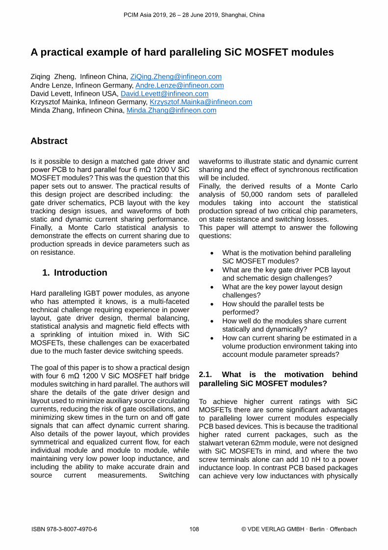
smaller power loop areas and utilizing the potential of laminated structures offered by multi-layer PCB’s. This coupled with ability to have low and equal gate inductances and very symmetrical internal chip layouts allows faster switching speeds to be achieved. The power PCB show in Figure 1 here has a measured inductance for the complete switching power loop of 19 nH per module resulting in <5 nH effective inductance for the combined switch.
Figure 1. Power PCB used for testing four modules
2.2. What are the key gate driver layout and schematic design challenges?
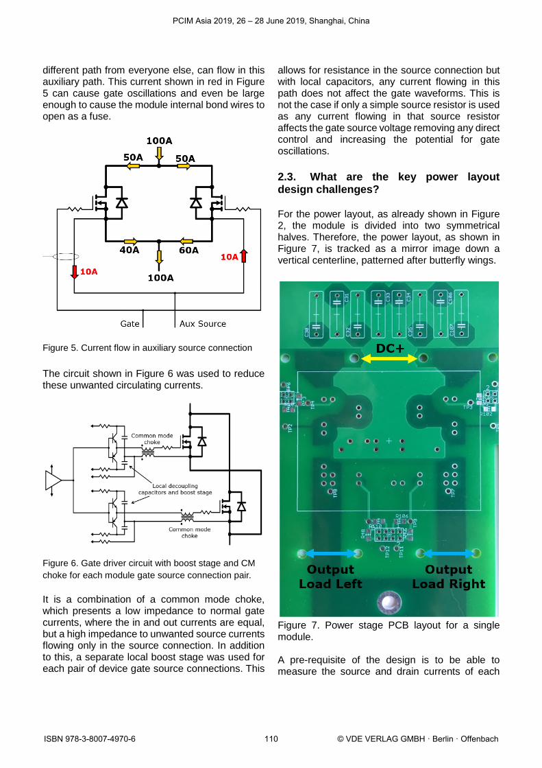
The 6 mΩ module pin out, shown in Figure 2, has a dual gate source, power drain and power source layout to reduce inductance and improve current sharing amongst the SiC MOSFET chips internal to the module. The first challenge of the gate layout is to have a symmetrical layout for both pairs of gate source connections.
Figure 2. Module pin out and schematic This symmetry is achieved by a mezzanine gate driver PCB mounted on top of the power PCB as
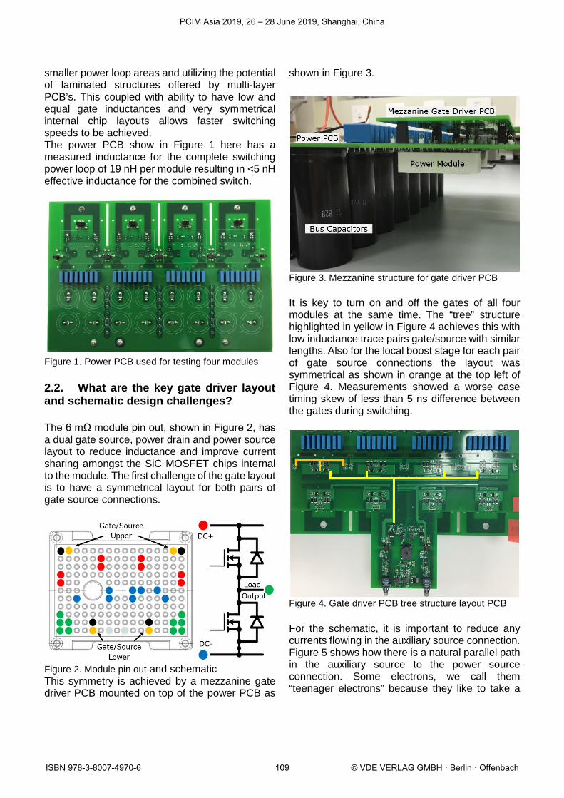
shown in Figure 3.
Figure 3. Mezzanine structure for gate driver PCB
It is key to turn on and off the gates of all four modules at the same time. The “tree” structure highlighted in yellow in Figure 4 achieves this with low inductance trace pairs gate/source with similar lengths. Also for the local boost stage for each pair of gate source connections the layout was symmetrical as shown in orange at the top left of Figure 4. Measurements showed a worse case timing skew of less than 5 ns difference between the gates during switching.
Figure 4. Gate driver PCB tree structure layout PCB
For the schematic, it is important to reduce any currents flowing in the auxiliary source connection. Figure 5 shows how there is a natural parallel path in the auxiliary source to the power source connection. Some electrons, we call them “teenager electrons” because they like to take a
PCIM Asia 2019, 26 – 28 June 2019, Shanghai, China
different path from everyone else, can flow in this auxiliary path. This current shown in red in Figure 5 can cause gate oscillations and even be large enough to cause the module internal bond wires to open as a fuse.
Figure 5. Current flow in auxiliary source connection
The circuit shown in Figure 6 was used to reduce these unwanted circulating currents.
Figure 6. Gate driver circuit with boost stage and CM
choke for each module gate source connection pair.
It is a combination of a common mode choke, which presents a low impedance to normal gate currents, where the in and out currents are equal, but a high impedance to unwanted source currents flowing only in the source connection. In addition to this, a separate local boost stage was used for each pair of device gate source connections. This
allows for resistance in the source connection but with local capacitors, any current flowing in this path does not affect the gate waveforms. This is not the case if only a simple source resistor is used as any current flowing in that source resistor affects the gate source voltage removing any direct control and increasing the potential for gate oscillations.
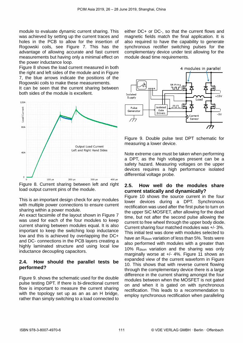
2.3. What are the key power layout design challenges?
For the power layout, as already shown in Figure 2, the module is divided into two symmetrical halves. Therefore, the power layout, as shown in Figure 7, is tracked as a mirror image down a vertical centerline, patterned after butterfly wings.
Figure 7. Power stage PCB layout for a single module.
A pre-requisite of the design is to be able to measure the source and drain currents of each
PCIM Asia 2019, 26 – 28 June 2019, Shanghai, China
module to evaluate dynamic current sharing. This was achieved by setting up the current traces and holes in the PCB to allow for the insertion of Rogowski coils, see Figure 7. This has the advantage of allowing accurate and fast current measurements but having only a minimal effect on the power inductance loop.Figure 8 shows the load current measured in both the right and left sides of the module and in Figure 7, the blue arrows indicate the positions of the Rogowski coils to make these measurements. It can be seen that the current sharing between both sides of the module is excellent.
Figure 8. Current sharing between left and right load output current pins of the module.
This is an important design check for any modules with multiple power connections to ensure current sharing within a power module. An exact facsimile of the layout shown in Figure 7 was used for each of the four modules to keep current sharing between modules equal. It is also important to keep the switching loop inductance low and this is achieved by overlapping the DC+ and DC- connections in the PCB layers creating a highly laminated structure and using local low inductance decoupling capacitors.
2.4. How should the parallel tests be performed?
Figure 9. shows the schematic used for the double pulse testing DPT. If there is bi-directional current flow is important to measure the current sharing with the topology set up as an as an H bridge, rather than simply switching to a load connected to
either DC+ or DC-, so that the current flows and magnetic fields match the final application. It is also required to have the capability to generate synchronous rectifier switching pulses for the complementary device under test allowing for the module dead time requirements.
Figure 9. Double pulse test DPT schematic for measuring a lower device.
Note extreme care must be taken when performing a DPT, as the high voltages present can be a safety hazard. Measuring voltages on the upper devices requires a high performance isolated differential voltage probe.
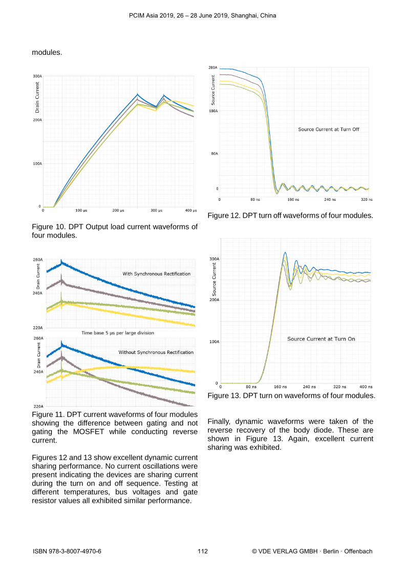
2.5. How well do the modules share current statically and dynamically?Figure 10 shows the source current in the four lower devices during a DPT. Synchronous rectification was used after the first pulse to turn on the upper SiC MOSFET, after allowing for the dead time, but not after the second pulse allowing the current to free wheel through the upper body diode. Current sharing four matched modules was +/- 3%.This initial test was done with modules selected to have an Rdson variation of less than 5%. Tests were also performed with modules with a greater than 10% Rdson variation and the sharing was only marginally worse at +/- 4%. Figure 11 shows an expanded view of the current waveform in Figure 10. This shows that with reverse current flowing through the complementary device there is a large difference in the current sharing amongst the four modules between when the MOSFET is not gated on and when it is gated on with synchronous rectification. This leads to a recommendation to employ synchronous rectification when paralleling
PCIM Asia 2019, 26 – 28 June 2019, Shanghai, China
Figure 10. DPT Output load current waveforms of four modules.
Figure 11. DPT current waveforms of four modules showing the difference between gating and not gating the MOSFET while conducting reverse current.
Figures 12 and 13 show excellent dynamic current sharing performance. No current oscillations were present indicating the devices are sharing current during the turn on and off sequence. Testing at different temperatures, bus voltages and gate resistor values all exhibited similar performance.
Figure 12. DPT turn off waveforms of four modules.
Figure 13. DPT turn on waveforms of four modules.
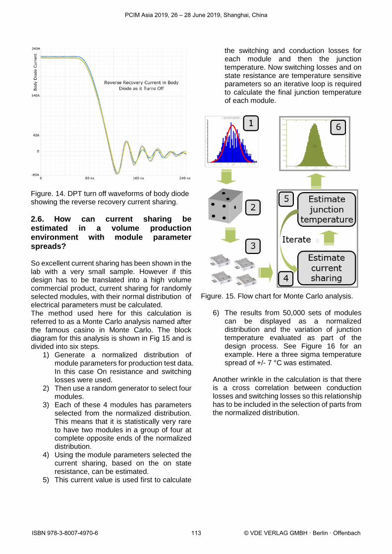
Finally, dynamic waveforms were taken of the reverse recovery of the body diode. These are shown in Figure 13. Again, excellent current sharing was exhibited.
PCIM Asia 2019, 26 – 28 June 2019, Shanghai, China
Figure. 14. DPT turn off waveforms of body diode showing the reverse recovery current sharing.
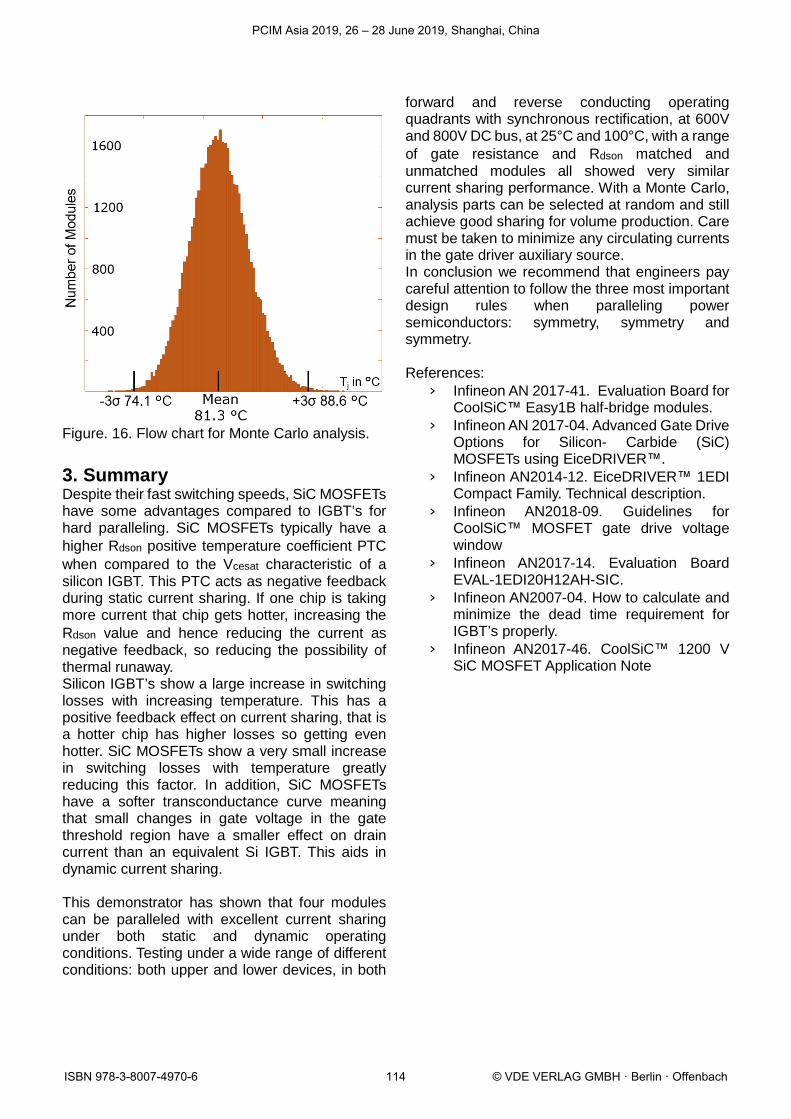
2.6. How can current sharing be estimated in a volume production environment with module parameter spreads?
So excellent current sharing has been shown in the lab with a very small sample. However if this design has to be translated into a high volume commercial product, current sharing for randomly selected modules, with their normal distribution of electrical parameters must be calculated.The method used here for this calculation is referred to as a Monte Carlo analysis named after the famous casino in Monte Carlo. The block diagram for this analysis is shown in Fig 15 and is divided into six steps.
1) Generate a normalized distribution of module parameters for production test data. In this case On resistance and switching losses were used.
2) Then use a random generator to select four modules.
3) Each of these 4 modules has parameters selected from the normalized distribution. This means that it is statistically very rare to have two modules in a group of four at complete opposite ends of the normalized distribution.
4) Using the module parameters selected the current sharing, based on the on state resistance, can be estimated.
5) This current value is used first to calculate
the switching and conduction losses for each module and then the junction temperature. Now switching losses and on state resistance are temperature sensitive parameters so an iterative loop is required to calculate the final junction temperature of each module.
Figure. 15. Flow chart for Monte Carlo analysis.
6) The results from 50,000 sets of modules can be displayed as a normalized distribution and the variation of junction temperature evaluated as part of the design process. See Figure 16 for an example. Here a three sigma temperature spread of +/- 7 °C was estimated.
Another wrinkle in the calculation is that there is a cross correlation between conduction losses and switching losses so this relationship has to be included in the selection of parts from the normalized distribution.
PCIM Asia 2019, 26 – 28 June 2019, Shanghai, China
3. Summary Despite their fast switching speeds, SiC MOSFETs have some advantages compared to IGBT’s for hard paralleling. SiC MOSFETs typically have a higher Rdson positive temperature coefficient PTC
when compared to the Vcesat characteristic of a silicon IGBT. This PTC acts as negative feedback during static current sharing. If one chip is taking more current that chip gets hotter, increasing the Rdson value and hence reducing the current as negative feedback, so reducing the possibility of thermal runaway. Silicon IGBT’s show a large increase in switching losses with increasing temperature. This has a positive feedback effect on current sharing, that is a hotter chip has higher losses so getting even hotter. SiC MOSFETs show a very small increase in switching losses with temperature greatly reducing this factor. In addition, SiC MOSFETs have a softer transconductance curve meaning that small changes in gate voltage in the gate threshold region have a smaller effect on drain current than an equivalent Si IGBT. This aids in dynamic current sharing.
This demonstrator has shown that four modules can be paralleled with excellent current sharing under both static and dynamic operating conditions. Testing under a wide range of different conditions: both upper and lower devices, in both
forward and reverse conducting operating quadrants with synchronous rectification, at 600V and 800V DC bus, at 25°C and 100°C, with a range of gate resistance and Rdson matched and unmatched modules all showed very similar current sharing performance. With a Monte Carlo, analysis parts can be selected at random and still achieve good sharing for volume production. Care must be taken to minimize any circulating currents in the gate driver auxiliary source. In conclusion we recommend that engineers pay careful attention to follow the three most important design rules when paralleling power semiconductors: symmetry, symmetry and symmetry.
References: › Infineon AN 2017-41. Evaluation Board for